

Page 1
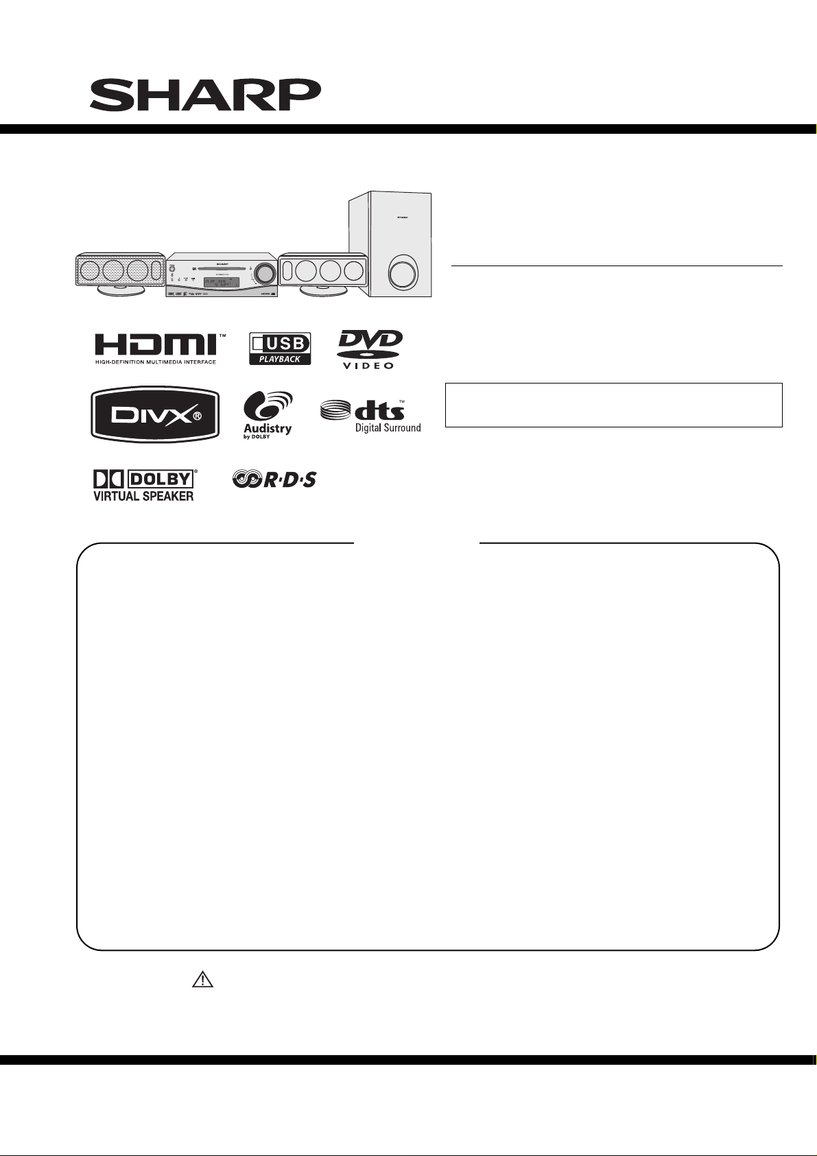
HT-DV40H
SERVICE MANUAL
No. SY756HTDV40HW
DVD CINEMA
CONTENTS
PRECAUTIONS FOR USING LEAD-FREE SOLDER
CHAPTER 1. GENERAL DESCRIPTION
[1] Safety Precaution For Service Manual ......... 1-1
[2] AC Power Supply Cord.................................. 1-2
[3] Specifications................................................ 1-2
[4] Names Of Parts.................................................... 1-4
CHAPTER 2. ADJUSTMENTS
[1] Servo Section ............................................... 2-1
[2] Test Mode .....................................................2-2
[3] DVD Test Mode............................................. 2-3
[4] DVD Firmware Update Test Mode................2-4
CHAPTER 3. MECHAN
[1] Caution On Disassembly ............................... 3-1
[2] Removing And Reinstalling The Main Parts . 3-4
CHAPTER 4. DIAGRAMS
[1] Main Block Diagrams..................................... 4-1
[2] DVD/CD Block Diagrams.............................. 4-3
[3] Power Block Diagrams .................................. 4-5
ISM BLOCKS
MODEL
HT-DV40H
[ Australia, Central & South America, Indonesia,
Singapore-Export/Vietnam, Middle East/Africa ]
HT-DV40H DVD Cinema consisting of HT-DV40H
(main unit), CP-DV40H (front speaker) and
CP-SW40H (subwoofer system).
• In the inte rests of user-safety (Required by safety regulations in
some countries) the set should be restored to its original
condition and only parts identical to those specified be used.
CHAPTER 5. CIRCUIT DESCRIPTION
[1] Waveforms Of DVD/CD Circuit......................5-1
[2] Voltage ..........................................................5-2
CHAPTER 6. CIRCUIT SCHEMATICS AND PARTS
LAYOUT
[1] Notes On Schematic Diagram.......................6-1
[2] Types Of Transistor And LED........................6-1
[3] Schematic Diagram.......................................6-2
[4] Wiring Side Of PWB....................................6-12
CHAPTER 7. FLOWCHART
[1] Troubleshooting.............................................7-1
CHAPTER 8. OTHERS
[1] Function Table Of IC......................................8-1
[2] FL Display .....................................................8-8
PARTS GUIDE
Parts marked with " " are important for maintaining the safety of the set. Be sure to replace these parts with specified
ones for maintaining the safety and performance of the set.
SHARP CORPORATION
This document has been published to be used
for after sales service only.
The contents are subject to change without notice.
Page 2
HT-DV40H
AudioXL-MP150Service ManualXLMP150MarketE
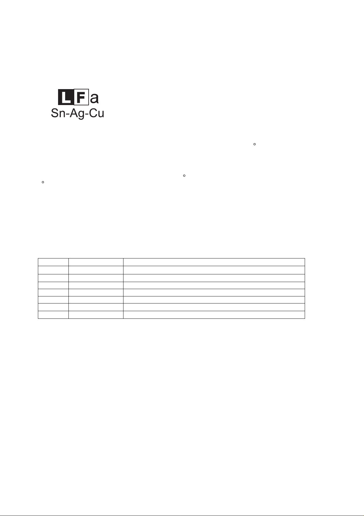
PRECAUTIONS FOR USING LEAD-FREE SOLDER
1. Employing lead-free solder
"MAIN, POWER, DISPLAY, SCART, VIDEO OUT, DIGITAL IN, DVD, SUBWOOFER PWB" of this model employs
lead-free solder.
The LF symbol indicates lead-free solder, and is attached on the PWB and service manuals. The alphabetical character
following LF shows the type of lead-free solder.
Example:
Indicates lead-free solder of tin, silver and copper.
2. Using lead-free wire solder
When fixing the PWB soldered with the lead-free solder, apply lead-free wire solder. Repairing with conventional lead wire
solder may cause damage or accident due to cracks.
As the melting point of lead-free solder (Sn-Ag-Cu) is higher than the lead wire solder by 40 C, we recommend you to
dedicatedsolderingbit,ifyou arenot familiarwith howto obtainlead-freewiresolderor solderingbit, contact our
use a
servicestation
3. Soldering
As themeltingpoint of lead-free solder(Sn-Ag-Cu) is about 220 C whichishigher than the conventional lead solder
by 40 C,
extended period of
of parts may be exceeded,
Lead-free solder contains more tin, and the end of the soldering bit may be easily corrected. Make sure to turn on
and off the
If a different type of solder stays on the tip of the soldering bit, it is alloyed with lead-free solder. Clean the bit after
every use
When the tip of the soldering bit is blackened during use, file it with steel wool or fine sandpaper.
Be careful when replacing parts with polarity indication on the PWB silk.
or service branch in your area.
and as it has poor solder wet ability, you may be apt to keep the soldering bit in contact with the PWB for
time. However, since the land may be peeled off or the maximum heat-resistance temperature
remove the bit from the PWB as soon as you confirm the steady soldering condition.
power of the bit as required.
of it.
Lead-free wire solder for servicing
Ref No.
PWB-A 92LPWB6891MANS MAIN
PWB-B 92LPWB6891PWRS POWER (B1), DISPLAY (B2), SCART (B3), VIDEO OUT (B4), DIGITAL IN (B5)
PWB-C 92LPWB6891DVDS DVD [ For Singapore-Export, Middle East / Africa ]
PWB-C 92LPWB6966DVDS DVD [ For Australia ]
PWB-C 92LPWB6968DVDS DVD [ For India ]
PWB-C 92LPWB7098DVDS DVD [ For Central & South America ]
PWB-D 92LPWB6891SWFS SUB WOOFER
Parts No.
Description
– i –
Page 3
HT-DV40H
CHAPTER 1: GENERAL DESCRIPTION
[1]
Safety Precaution For Service Manual
WARNINGS
THE AEL (ACCESSIBLE EMISSION LEVEL) OF LASER POWER OUTPUT FOR THIS MODEL IS SPECIFIED TO
BE LOWER THAN CLASS I REQUIREMENTS. HOWEVER, THE FOLLOWING PRECAUTIONS MUST BE OBSERVED
DURING SERVICING TO PROTECT YOUR EYES AGAINTS EXPOSURE TO THE LASER BEAM.
1- WHEN THE CABINET HAS BEEN REMOVED, THE POWER IS TURNED ON WITHOUT A COMPACT DISC,
AND THE PICKUP IS ON A POSITION OUTER THAN THE LEAD-IN POSITION, THE LASER WILL LIGHT FOR
SEVERAL SECONDS TO DETECT A DISC.
DO NOT LOOK INTO THE PICKUP LENS.
2- THE LASER POWER OUTPUT OF THE PICKUP INSIDE THE UNIT AND REPLACEMENT SERVICE PARTS
HAVE ALREADY BEEN ADJUSTED PRIOR TO SHIPPING.
3- NO ADJUSTMENT TO THE LASER POWER SHOULD BE ATTEMPTED WHEN REPLACING OR SERVICING
THE PICKUP.
4- UNDER NO CIRCUMSTANCES LOOK DIRECTLY INTO THE PICKUP LENS AT ANY TIME.
5- CAUTION - USE OF CONTROLS OR ADJUSTMENTS, OR PERFORMANCE OF PROCEDURES OTHER THAN
THOSE SPECIFIED HEREIN MAY RESULT IN HAZARDOUS RADIATION EXPOSURE.
This product is classified as a CLASS 1 LASER PRODUCT.
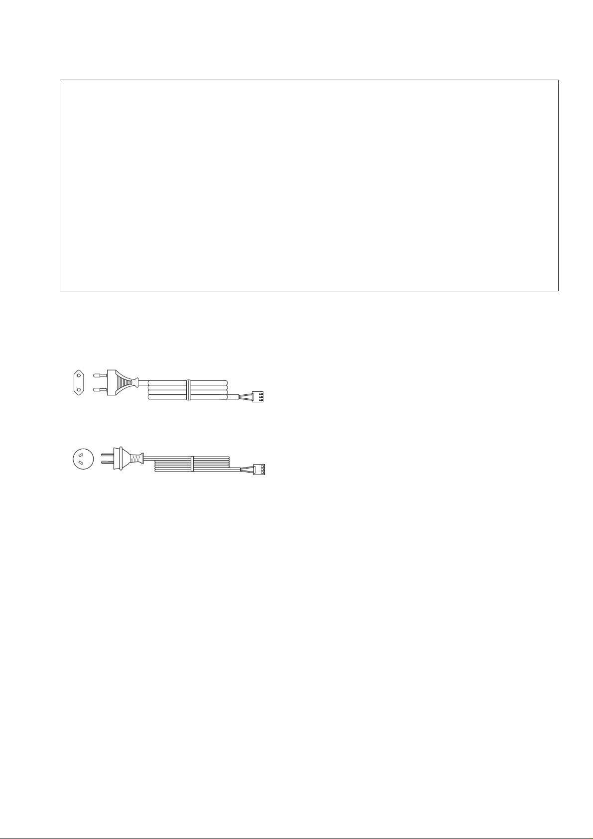
[2] AC Power Supply Cord
QACCEA001AW00
QACCLA001AW00
1 – 1
Page 4
HT-DV40H
[3]
Specifications
HT-DV40H except Australia
Main Unit USB
Power source AC 220 - 240 V ~ 50 Hz
Power
consumption
Output power
Video output
terminals
Audio input
terminals
Audio output
terminals
Dimensions Width: 300 mm (11-13/16")
Weight 3.8 kg (8.4 lbs.)
(*) This power consumption value is obtained when the
demonstration mode is cancelled in the power stand-by mode.
Power on: 82 W
Power stand-by: 0.6 W (*)
Front Speaker:
MPO: 150 W (75 W + 75 W) (10% T.H.D.)
RMS: 150 W (75 W + 75 W) (10% T.H.D.)
RMS: 90 W (45 W + 45 W) (0.9% T.H.D.)
Subwoofer:
MPO: 100 W (10% T.H.D.)
RMS: 100 W (10% T.H.D.)
RMS: 55 W (0.9% T.H.D.)
SCART output: SCART terminal x 1
Video output: RCA type x 1
S-video output: S-terminal x 1
Component video output: (Y/P
HDMI output : HDMI x 1
Support 480p/570p/1080i output formats.
Optical digital input (DIGITAL 1): Square type x 1
Optical digital input (DIGITAL 2): Square type x 1
Analogue input : 500 mV/47k ohms
Speakers: 4 ohms
Subwoofer: 12 ohms
Headphones: 16 - 50 ohms
(recommended: 32 ohms)
Height: 106 mm (4-1/8")
Depth: 300 mm (11-13/16")
B/PR
) x 1
USB host
interface
Support file MPEG 1 Layer 3
Bitrate support MP3 (32 - 320 kbps)
Other Maximum total number of MP3/WMA files is
File system
support
Complies with USB 1.1/2.0 (Full Speed)
Mass-Storage-Class.
Support Bulk only and CBI protocol.
MPEG 2 Layer 3
WMA (Non DRM)
WMA (64 - 160 kbps)
1200.
The ID3TAG information supported are
TITLE, ARTIST and ALBUM only.
Support ID3TAG version 1 and version 2.
Support USB devices with Microsoft
Windows/DOS/FAT 12/FAT 16/FAT 32.
2 kbyte block length for sector.
Subwoofer
Type Subwoofer system
Maximum input
power
Rated input power 100 W
Impedance 12 ohms
Dimensions Width: 220 mm (8-11/16")
Weight 7.6 kg (16.7 lbs.)
20 cm (8 ") subwoofer
200 W
Height: 354 mm (13-15/16")
Depth: 438 mm (17-1/4")
DVD player
Signal system PAL/NTSC colour
Supported disc
types
Video signal Horizontal resolution: 500 lines
Audio signal Frequency
DVD (with the same region number on the
back of the unit), audio CD, CD-R, CD-RW,
JPEG, DivX (version 3.0 ~ 6.0)
S/N ratio: 70 dB
characteristics
S/N radio CD: 94 dB (1 kHz)
Dynamic range Linear PCM DVD: 95 dB
Total harmonic
distortion ratio
Linear PCM DVD:
20 Hz to 20 kHz
(sampling rate: 48 kHz)
20 Hz to 20 kHz
(sampling rate: 96 kHz)
CD: 20 Hz to 20 kHz
CD: 94 dB
0.01% maximum
Speaker
Type 2-way type speaker system
Maximum input
power
Rated input power 75 W
Impedance 4 ohms
Dimensions Width: 300 mm (11-13/16")
Weight 2.1 kg (4.6 lbs.)/each
2.5 cm (1") tweeter
8 cm (3-1/8") woofer (x 2)
150 W
Height: 129 mm (5-1/16")
Depth: 160 mm (6-5/16")
Tuner
Frequency
range
Other Maximum station can be stored is 30 preset.
FM: 87.5 - 108 MHz
1 – 2
Page 5
HT-DV40H for Australia
HT-DV40H
Main Unit
Power source AC 220 - 240 V ~ 50 Hz
Power
consumption
Output power Speaker:
Video output
terminals
Audio input
terminals
Audio output
terminals
Dimensions Width: 300 mm (11-13/16")
Weight 3.8 kg (8.4 lbs.)
(*) This power consumption value is obtained when the
demonstration mode is cancelled in the power stand-by mode.
Power on: 82 W
Power stand-by: 0.6 W (*)
RMS: 150 W (75 W + 75 W) (10% T.H.D.)
RMS: 90 W (45 W + 45 W) (0.9% T.H.D.)
Subwoofer:
RMS: 100 W (10% T.H.D.)
RMS: 55 W (0.9% T.H.D.)
SCART output: SCART terminal x 1
Video output: RCA type x 1
S-video output: S-terminal x 1
Component video output: (Y/P
HDMI output : HDMI x 1
Support 480p/570p/1080i output formats.
Optical digital input (DIGITAL 1): Square type x 1
Optical digital input (DIGITAL 2): Square type x 1
Analogue input : 500 mV/47 k ohms
Speakers: 4 ohms
Subwoofer: 12 ohms
Headphones: 16 - 50 ohms
(recommended: 32 ohms)
Height: 106 mm (4-1/8")
Depth: 300 mm (11-13/16")
B/PR
) x 1
DVD player
Signal system PAL/NTSC colour
Supported disc
types
Video signal Horizontal resolution: 500 lines
Audio signal Frequency
DVD (with the same region number on the
back of the unit), audio CD, CD-R, CD-RW,
JPEG, DivX (version 3.0 ~ 6.0)
S/N ratio: 70 dB
characteristics
S/N radio CD: 94 dB (1 kHz)
Dynamic range Linear PCM DVD: 95 dB
Total harmonic
distortion ratio
Linear PCM DVD:
20 Hz to 20 kHz
(sampling rate: 48 kHz)
20 Hz to 20 kHz
(sampling rate: 96 kHz)
CD: 20 Hz to 20 kHz
CD: 94 dB
0.01% maximum
USB
USB host
interface
Support file MPEG 1 Layer 3
Bitrate support MP3 (32 - 320 kbps)
Other Maximum total number of MP3/WMA files is
File system
support
Complies with USB 1.1/2.0 (Full Speed)
Mass-Storage-Class.
Support Bulk only and CBI protocol.
MPEG 2 Layer 3
WMA (Non DRM)
WMA (64 - 160 kbps)
1200.
The ID3TAG information supported are
TITLE, ARTIST and ALBUM only.
Support ID3TAG version 1 and version 2.
Support USB devices with Microsoft
Windows/DOS/FAT 12/FAT 16/FAT 32.
2 kbyte block length for sector.
Subwoofer
Type Subwoofer system
Maximum input
power
Rated input power 100 W
Impedance 12 ohms
Dimensions Width: 220 mm (8-11/16")
Weight 7.6 kg (16.7 lbs.)
20 cm (8 ") subwoofer
200 W
Height: 354 mm (13-15/16")
Depth: 438 mm (17-1/4")
Tuner
Frequency
range
Other Maximum station can be stored is 30 preset.
FM: 87.5 - 108 MHz
Speaker
Type 2-way type speaker system
Maximum input
power
Rated input power 75 W
Impedance 4 ohms
Dimensions Width: 300 mm (11-13/16")
Weight 2.1 kg (4.6 lbs.)/each
2.5 cm (1") tweeter
8 cm (3-1/8") woofer (x 2)
150 W
Height: 129 mm (5-1/16")
Depth: 160 mm (6-5/16")
1 – 3
Page 6
HT-DV40H
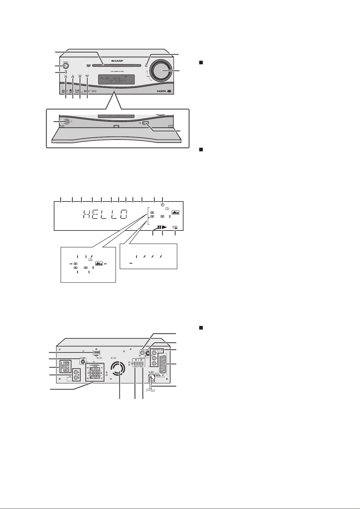
[4] Names Of Parts
1
2
3
67
5
4
8
1 2 3 4
FOLDTITLECHAP
13
1415
DAILY
DIGITAL
16 17
VS PL
18 19
MP3
ST
DOOR OPEN
6 7 8910 11
5
WMA
RDS TA PTYI TP
24
12
TOT AL
SLEEP
DAILY
DIGITAL
VS PL
MTS
IVC NB SS
MEMORY
MHz
262527
20 21 22 23
IVC NB SS
MTS
MEMORY
9
Front panel
10
1. CD Compartment
2. On/Stand-by Button
3. Timer Indicator
4. DVD/CD/USB Play/Pause Button
5. Disc or USB Stop Button
6. Function Button
7. Remote Sensor
8. Headphone Socket
9. Disc Open/Close Button
10. Volume Control
11. USB Terminal
11
Display
1. Chapter Indicator
2. Title Indicator
3. Folder Indicator
4. MP3 Indicator
5. WMA Indicator
6. RDS Indicator
7. Traffic Announcement Indicator
8. Dynamic PTY Indicator
ST
A1
B
9. Traffic Programme Indicator
10. Total Indicator
11. Sleep Indicator
12. Timer Play Indicator
13. Daily Timer Indicator
14. FM Stereo Mode Indicator
15. FM Stereo Receiving Indicator
16. Dolby Digital Signal Indicator
17. DTS Indicator
18. Dolby Virtual Speaker Indicator
19. Dolby Pro Logic II Indicator
20. Mono to Stereo Indicator
21. Intelligent Volume Indicator
22. Natural Bass Indicator
23. Sound Space Indicator
24. Memory Indicator
25. Disc or USB Pause Indicator
26. Disc or USB Play Indicator
27. Disc or USB Repeat Indicator
9
10
1
2
3
11
12
4
5
6
87
13
1. HDMI Socket
2. FM 75 Ohms Aerial Socket
3. Subwoofer Terminals
4. Auxiliary Input Sockets
5. Front Speaker Terminals
6. Cooling Fan
7. Optical Digital Input 1 Socket
8. Optical Digital Input 2 Socket
9. Video Output Socket
10. S-Video Output Socket
11. Component Video Out Sockets
12. SCART Output Socket (Audio + Video)
13. AC Power Lead
1 – 4
Rear panel
Page 7
15
16 17 18
10
11
12
13
14
19
20
21
22
HT-DV40H
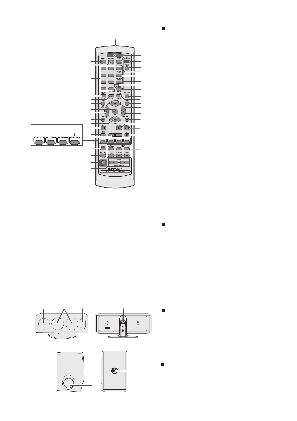
Remote control
1
23
2
3
4
5
6
1
4
7 8 9
3
2
6
5
+100
7
8
9
24
25
26
27
28
29
30
31
32
33
34
35
36
37
38
39
40
1.Remote Control Transmitter
2.DVD Direct Button
3.DVD On Screen Button
4.Direct Search Buttons
5.Memory or Dimmer Button
6.DVD/CD/MP3/WMA Repeat Button
7.Menu Button
8.Enter Button
9.Cursor Left Button
10.
DVD Chapter Skip/DVD/MP3/WMA Fast Reverse/CD/MP3/WMA
Track Down/Tuner Preset Down and Time Down Button
11.
Tuning Down or Cursor Down Button
12.USB Play or Pause Button
13.Video Mode Button
14.DVD/CD/MP3/WMA/Stop Button
15.DVD/CD/MP3/WMA Button
16.USB Button
17.Auxiliary Button
18.Tuner Button
19.Audio Button
20.
Dolby Virtual Speaker Button
21.Shift Button
22.Volume Up or Down Buttons
23.Clear or Display Button
24.On/Stand-by Button
25.Clock or Timer Button
30.DVD Angle Button
31.DVD Subtitle Button
32.DVD Zoom Button
33.Return Button
34.Tuning Up or Cursor Up Button
35.Cursor Right Button
36.DVD Chapter Skip/DVD/MP3/WMA Fast Forward/CD/MP3/
WMA Track Up/Tuner Preset Up and Time Up Button
37.DVD Slow Button
38.DVD/CD/MP3/WMA Play or Pause Button
39.DVD/CD/MP3/WMA Still Button
40.TV Operation Buttons
123 4
LEFT
1
3
2
Remote control with shift button
2.RDS ASPM Button
3.RDS PTY Button
5.Set Up Button
6.A-B Repeat Button
7.Top Menu Button
20.Demo Button
22.Subwoofer level
23.RDS DISP Button
26.Sound Space Buton
27.
Natural Bass Button
28.
Intelligent Volume Button
29.Sound Mode Button
Mono to Stereo Button
30.
32.
Random Button
-
or + Button
Speaker system (CP-DV40H)
1.Tweeter
2.Woofers
3.Bass Reflex Duct
4.Speaker Terminals
Subwoofer (CP-SW40H)
1.Subwoofer
2.Bass Reflex Duct
3.Speaker Terminals
1 – 5
Page 8

HT-DV40H
CD-ES700/CD-ES77CD-ES700/CD-ES77Service ManualCD-ES700/CD-ES77MarketE
CHAPTER 2. ADJUSTMENTS
[1] Servo Section
• Adjustment
Since this DVD system incorporates the following
automatic adjustment functions, readjustment is
not needed when replacing the pickup. Therefore,
different PWBs and pickups can be combined
freely. Each time a disc is changed, these
adjustments are performed automatically.
Therefore, playback of each disc can be performed
under optimum conditions.
Items adjusted automatically
1) Offset adjustment (The offset voltage between the
head amplifier output and the VREF reference
voltage is compensated inside the IC.)
* Focus offset adjustment
* Tracking offset adjustment
2) Tracking balance adjustment
3) Gain adjustment (The gain is compensated inside
the IC so that the loop gain at the gain crossover
frequency will be 0 dB.)
* Focus gain adjustment
* Tracking gain adjustment
2 – 1
Page 9

HT-DV40H
[2] Test Mode
1.Test Mode Functions
1.1.Entering the Test Mode
While holding down both the n button and the ON/STAND-BY button of the main unit from the AC Supply O ff state,
turn the AC Supply ON to enter the Test Menu Mode.
[ n ] + [ ON/STAND-BY ] [ AC ON ]
1.2.TEST Mode Processing
* When entering the TEST Mode, the ROM version are displa ye d as follow s.
* System micom version on the FL display upper row : HDH**** ( **** : Version No )
* DVD Firmware version on the FL display lower row : SRCV** ( ** : Version No )
1.3.TEST Mode button
* Press direct designation button or turn VOL Jog during the version display to enter the sp ecified TEST Mode as
shown below.
* exit test mode by ON/STAND-BY key during micom version display
TEST MODE TEST MODE PROCEDURE TO ENTER
TEST 15 DVD TEST
TEST 16 FIRMWARE UPDATE TEST Direct press [PLAY] key during version display.
Turn VOL Jog to select "DVD TEST" during version
display, then press [STOP] key to enter.
1.4.Canceling TEST Mode
Press the ON / STAND-BY button in each TEST Mode.
2 – 2
Page 10
HT-DV40H
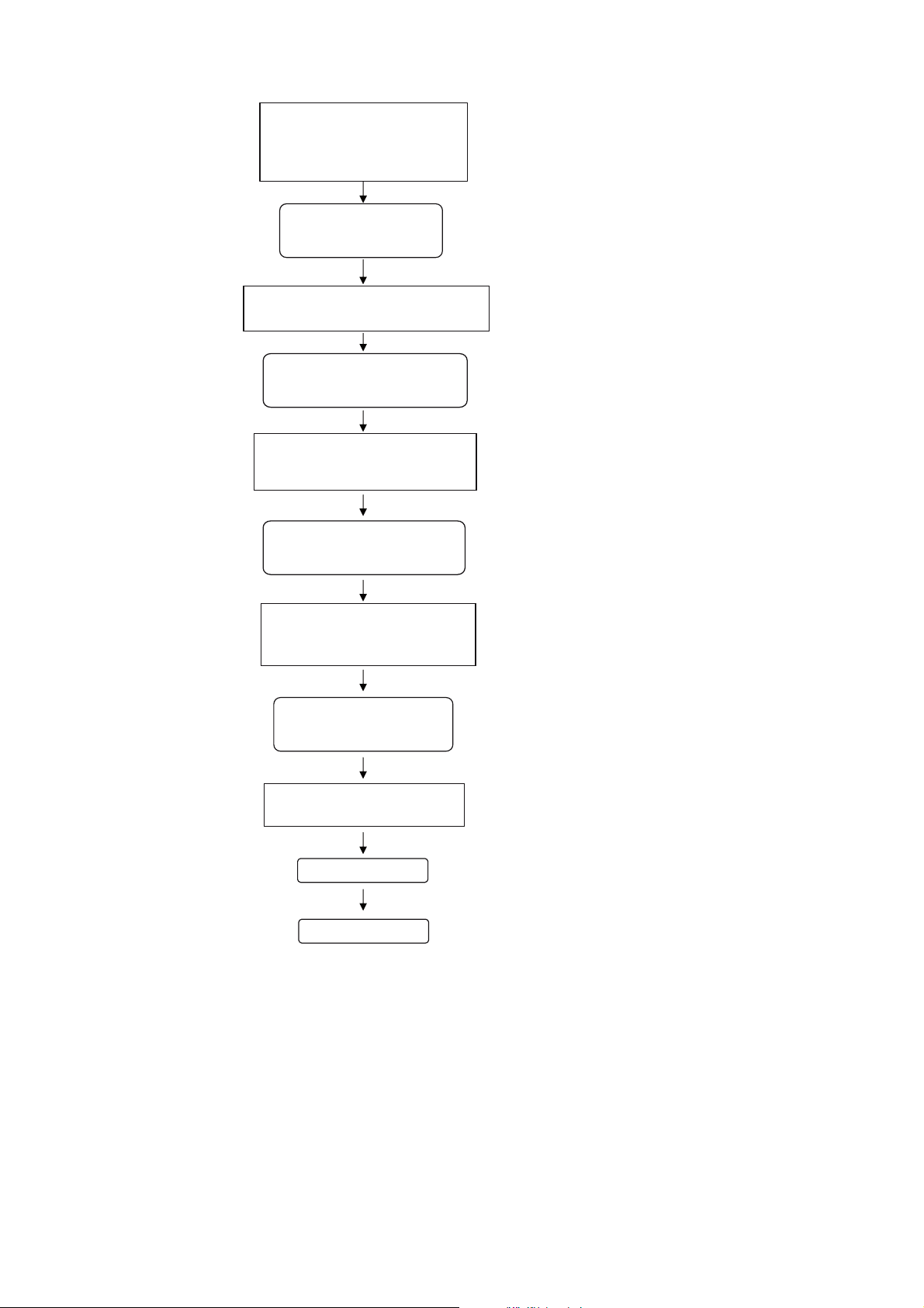
[3] DVD Test Mode
[STEP 1]
At testmode menu, select
"DVD TEST MODE" by
turning VOL Jog UP and Down
and press [STOP] key to enter
dvd test mode
[STEP 2]
[STEP 3]
[STEP 4]
[STEP 5]
[STEP 6]
[STEP 7]
"DVD TEST", will appear in
unit display
Press [DVD/CD] key at remote control to
turn ON CD Laser
"CD_LASER_ON" appear in unit
display
Press again [DVD/CD] key at remote
control, this time to turn ON DVD
Laser
"DVD_LASER ON" appear in unit
display
Press again [DVD/CD] key at remote
control, this time to turn OFF the
laser
Note 1:
In dvd test mode, DVD start up in cd mode
but no need to do disc reading process
[STEP 8]
[STEP 9]
[STEP 10]
[STEP 11]
"LASER OFF" appear in unit
display
Press ON/STAND-BY key to exit
the test mode.
EXIT the test mode
END
2 – 3
Page 11
[4] DVD Firmware Update Test Mode
HT-DV40H
After enter testmode menu, press
[PLAY] key at main unit to select
"FW UPDATE TEST MODE" to
enter this mode
"FW_UPDATE_" will appear on upper row of
unit display and current firmware version DVD
will appear on lower row of unit display as
"FW_SRCV **"
Plug in USB device
When enter firmware upgrade menu,
unit display at lower row change to
"FW_SRCV_ **" blinking at 2Hz
Press ENTER
key to start F/W upgrade.
Note 1:
To enter testmode, during AC supply off
condition, whilst pressing down STOP key and
ON/STAND-BY key together, turn ON AC Supply.
Note 2:
Make sure there is "DVDROM.bin" file inside the usb device
After ENTER key is pressed,
unit display at lower row will show
"_UPDATING_" blinking display
After update process completed,
new firmware version will be
displayed in unit display lower row as
"FW_SRCV_ **"
User press [ON/STAND-BY]
key to exit this testmode
END
Note 3:
"_UPDATING_" blinking display means DVD
firmware upgrade is in progress.
During firmware upgrading is in progress, do not
POWER OFF the unit!
2 – 4
Page 12
HT-DV40H
Amp abnormal detection and System PROTECTION display
In case amp abnormal detection or System PROTECTION had occurred, the unit will automatically enter to stand-by
mode and Timer indicator will flashing as below.
Example : In case of amp abnormal
FLASHING
OFF
TIMER
LED
ON
OFF
NO. 1
NO. 1 : System Protect
NO. 2 : Amp abnormal
NO. 3 : DVD +B Protect
NO. 4 : FAN LOCK detection
OFF
FLASHING
OFF
NO. 2 NO. 2
1 FRAME
ON ON ON
NO. 3
OFF
NO. 4 NO. 1
OFF
(REPEAT)
Software RESET.
Function: - Software RESET ( Press Eject + ON / STAND-BY key while set at Standby mode ).
All the function condition will be initialize.
After display "CLEAR ALL", the unit will shows demo display.
BEFORE TRANSPORTING THE UNIT
The following process need to be taken after set tapering / parts replacement.
1. Press the ON / STAND-BY button to power on the unit.
2. Select DVD / CD function, then press [SHIFT]+[SETUP] key at remote control to enter DVD SETUP menu.
3. Use cursor up / down key to select DEFAULT, then press cursor RIGHT key to select "RESTORE".
4. While cursor is highlited at "RESTORE" press ENTER key.
5. After that select "EXIT SETUP" and press ENTER key.
6. Press the ON / STAND-BY button to enter standby mode.
7. While pressing down EJECT button, press the ON / STAND-BY button. "CLEAR ALL" will be display at FL.
8. Unplug the AC cord and the unit is ready for transporting.
Note:
Connect this unit to TV in order to view step no 1 ~ 5.
2 – 5
Page 13

-MEMO-
HT-DV40H
2 – 6
Page 14
HT-DV40H
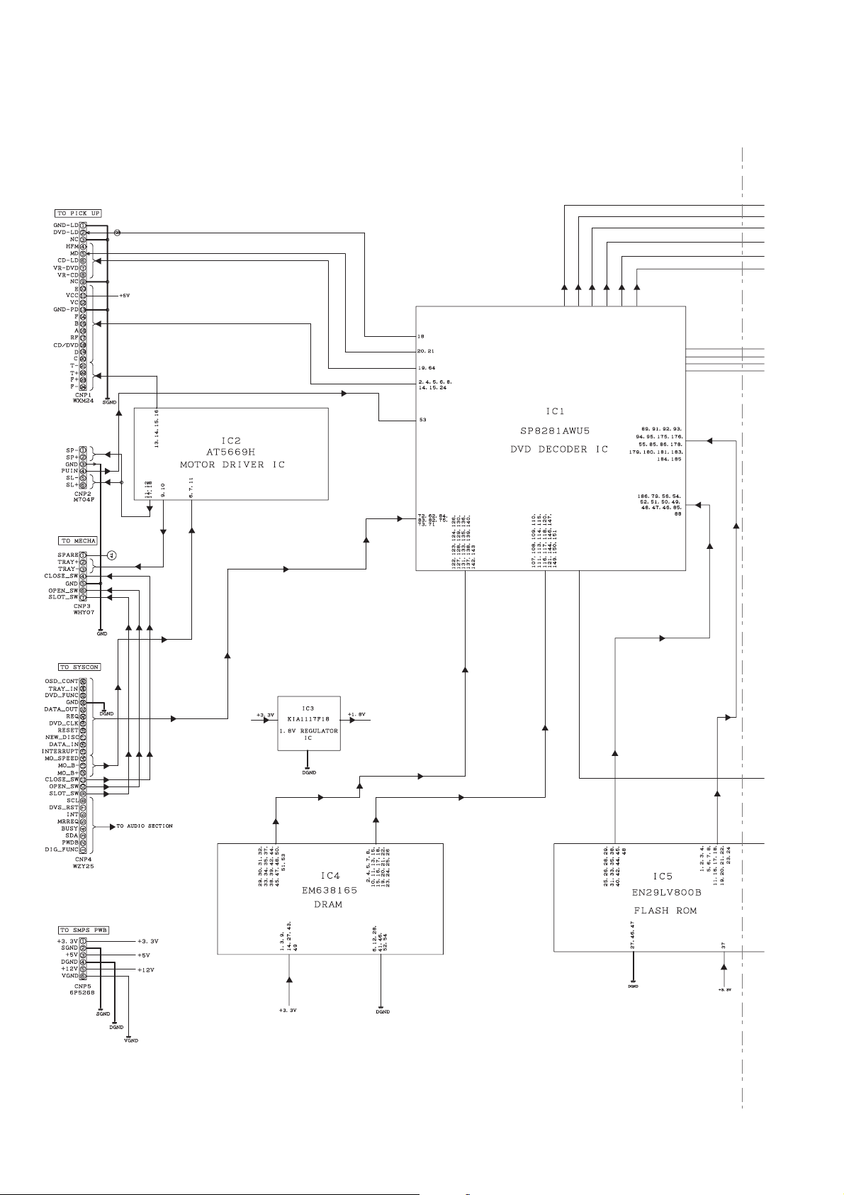
CHAPTER 4. DIAGRAM
[1] Main Block Diagrams
(TP1)
1234
TO DVD PWB
Figure 4-1: MAIN BLOCK DIAGRAM (1/2)
4 – 1
Page 15
HT-DV40H
IC701
IXA161AW00
PR
Y
PB
S01
Figure 4-2: MAIN BLOCK DIAGRAM (2/2)
4 – 2
Page 16
HT-DV40H
[2] DVD/CD Block Diagrams
199
198
196
201
203
204
211
218
219
221
194
Figure 4-3: DVD/CD BLOCK DIAGRAM (1/2)
4 – 3
Page 17
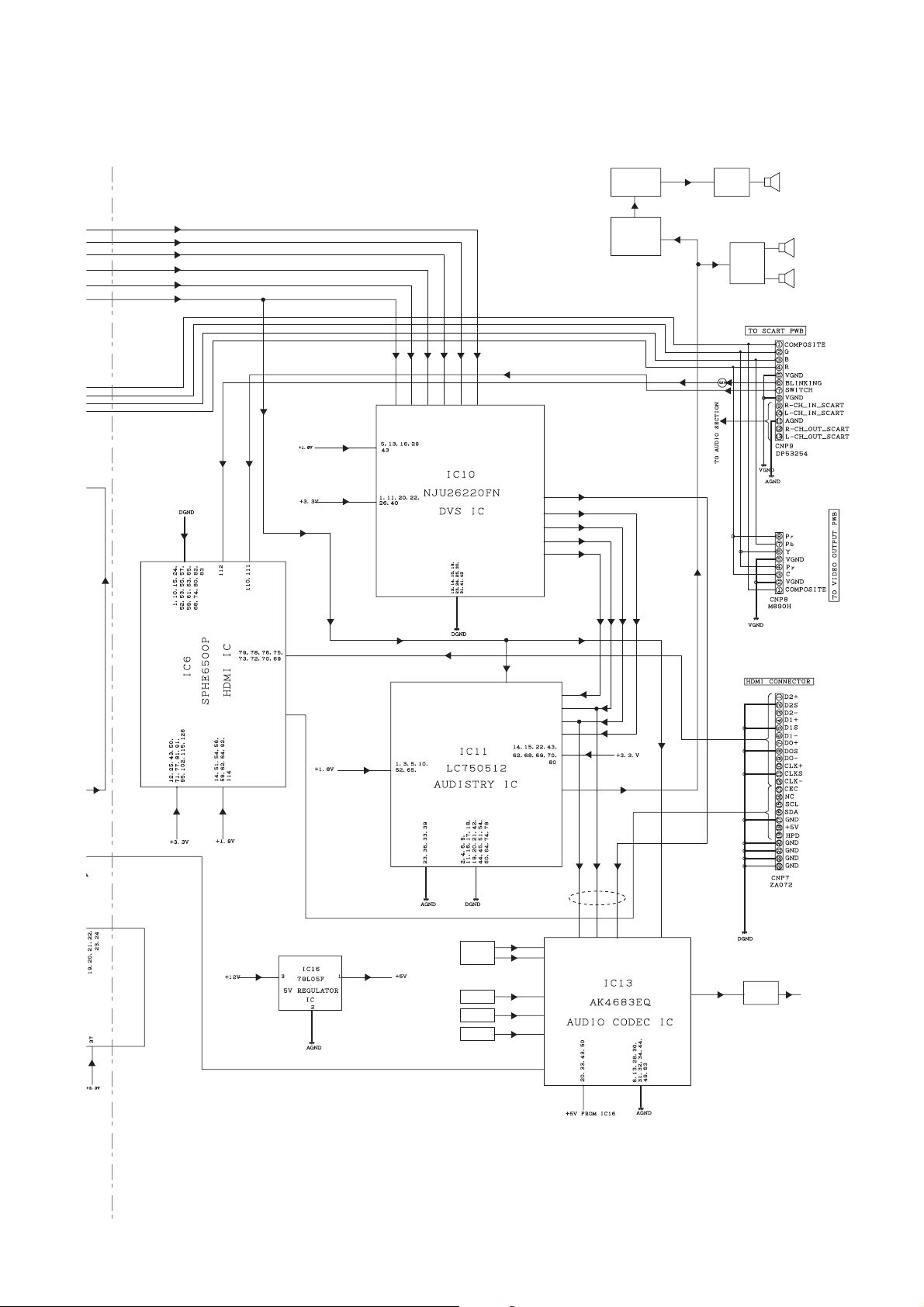
HT-DV40H
18
2
484645
MIX
LPF
VOL
NJU7391
(2/2)
44
39
33
34
35
38
Power
Amp
Buffer
Amp
S.W.
Lch
Rch
Analog
Signal
OPT 1
OPT 2
COAX
38
35
34
33
27,32
FOR
SCART
SIGNAL
52
23
24
2914
1551
40, 41
Buffer
Amp
TO
SCART
Figure 4-4: DVD/CD BLOCK DIAGRAM (2/2)
4 – 4
Page 18
HT-DV40H
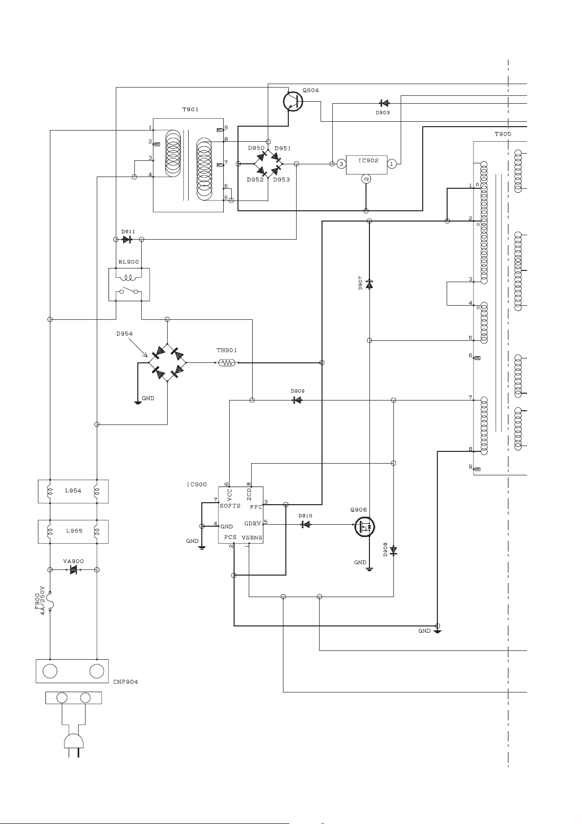
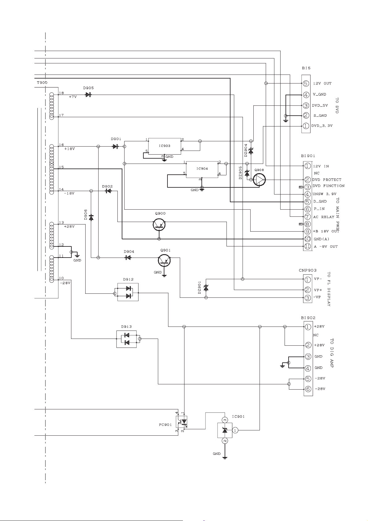
[3] Power Block Diagrams
AC SUPPLY
220-240V ~ 50Hz
Figure 4-5: POWER BLOCK DIAGRAM (1/2)
4 – 5
Page 19
HT-DV40H
Figure 4-6: POWER BLOCK DIAGRAM (2/2)
4 – 6
Page 20
HT-DV40H
CHAPTER 5.
CIRCUIT DESCRIPTION
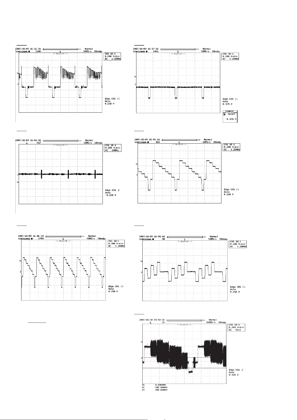
[1] Waveform of CD / DVD Circuit
WF1
WF3
VIDEO OUT
S-VIDEO OUT - C OUT
WF2
WF4
S-VIDEO - Y OUTPUT
COMPONENT VIDEO OUT - Y Output
(Interlace mode)
WF5
COMPONENT VIDEO OUT - Y Output
(P-Scan mode) (Interlace mode)
* NOTE:
WF1 ~ WF3 : Power On (stop) Mode.
WF4 ~ WF8 : DVD Test Disc TDV-540A.
(Colour Bar 75%)
WF6
WF7
COMPONENT VIDEO OUT - Pb/Cb Output
VIDEO OUT
5 – 1
Page 21
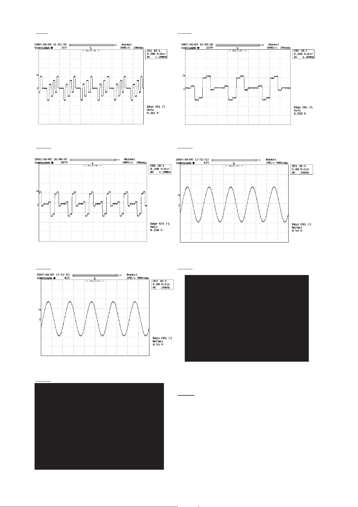
WF8 COMPONENT VIDEO OUT - Pb/Cb Output WF9 COMPONENT VIDEO OUT - Pr/Cr Output
(P-Scan mode) (Interlace mode)
WF10 COMPONENT VIDEO OUT - Pr/Cr Output WF11 Audio Left
(P-Scan mode)
HT-DV40H
WF12 Audio Right WF13 RF Signal (CD)
WF14 RF Signal (DVD)
* Note:
WF9 ~ WF10 : DVD Test Disc TDV-540A
(Colour Bar 75%)
WF11 ~ WF12 : DVD/CD Test Disc 1KHz, 0db.
WF13 ~ WF14 : Nomal Disc
5 – 2
Page 22
HT-DV40H
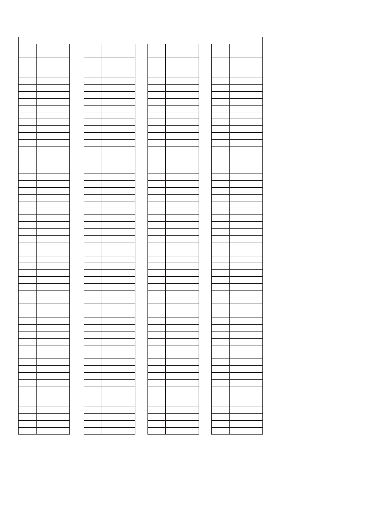
[2] Voltage
IC1 ( VHiSP8281AWU5 )
PINNOVOLTAGE
(V)
1 1.65 56 3.26 111 1.99 166 3.52
2 1.67 57 3.26 112 3.27 167 3.24
3 0.93 58 1.63 113 1.30 168 0.00
4 2.07 59 1.63 114 1.27 169 0.00
5 2.09 60 0.00 115 3.12 170 3.43
6 2.06 61 0.00 116 3.00 171 3.85
7 2.06 62 4.34 117 2.97 172 3.34
8 2.06 63 3.26 118 2.74 173 4.95
9 2.09 64 3.26 119 0.00 174 4.97
10 2.06 65 0.00 120 2.74 175 1.14
11 2.06 66 1.74 121 0.00 176 3.24
12 2.06 67 3.62 122 1.69 177 3.24
13 1.67 68 4.10 123 0.42 178 3.23
14 2.08 69 3.94 124 2.12 179 2.45
15 2.09 70 3.20 125 1.78 180 0.00
16 0.00 71 3.20 126 0.42 181 0.00
17 0.00 72 0.00 127 0.29 182 1.77
18 3.24 73 0.00 128 0.40 183 0.00
19 2.24 74 3.24 129 0.00 184 0.00
20 1.08 75 3.13 130 1.73 185 0.00
21 1.08 76 0.00 131 0.00 186 0.00
22 3.24 77 2.72 132 3.21 187 3.52
23 3.24 78 3.13 133 1.75 188 3.85
24 2.25 79 3.29 134 0.00 189 3.25
25 1.54 80 3.18 135 0.06 190 3.26
26 3.24 81 3.19 136 0.18 191 3.25
27 1.54 82 3.24 137 0.12 192 0.00
28 3.05 83 3.25 138 0.12 193 0.03
29 2.30 84 3.27 139 0.00 194 0.00
30 2.81 85 0.00 140 3.28 195 1.61
31 0.94 86 0.00 141 0.20 196 0.00
32 0.95 87 0.65 142 0.19 197 3.23
33 0.95 88 0.05 143 0.00 198 0.00
34 1.65 89 0.90 144 1.78 199 0.00
35 1.53 90 1.77 145 3.07 200 5.08
36 1.53 91 3.00 146 3.19 201 1.62
37 1.63 92 0.20 147 2.74 202 0.00
38 1.63 93 3.05 148 0.00 203 1.62
39 1.62 94 3.05 149 0.00 204 1.62
40 0.00 95 0.13 150 0.00 205 3.68
41 3.26 96 3.29 151 0.05 206 3.24
42 3.25 97 3.11 152 3.89 207 2.62
43 1.62 98 1.62 153 3.87 208 1.61
44 1.62 99 1.62 154 3.96 209 1.64
45 1.71 100 3.21 155 3.88 210 1.62
46 1.67 101 0.00 156 3.24 211 0.51
47 1.67 102 0.00 157 3.62 212 3.23
48 1.62 103 0.00 158 3.63 213 0.00
49 1.67 104 3.14 159 3.24 214 0.00
50 1.62 105 0.00 160 3.24 215 0.00
51 1.65 106 1.75 161 3.27 216 3.22
52 1.64 107 1.76 162 3.17 217 0.00
53 1.66 108 2.57 163 1.77 218 0.58
54 1.66 109 1.26 164 3.24 219 1.55
55 3.26 110 1.28 165 3.16 220 3.25
PINNOVOLTAGE
(V)
PINNOVOLTAGE
(V)
PINNOVOLTAGE
(V)
5 – 3
Page 23
IC1 ( VHiSP8281AWU5 )
PINNOVOLTAGE
(V)
221 1.55 230 1.46 239 0.61 248 3.11
222 0.00 231 2.00 240 0.63 249 0.24
223 0.00 232 1.18 241 0.04 250 2.41
224 0.00 233 1.22 242 2.96 251 1.09
225 2.88 234 3.18 243 0.00 252 0.87
226 1.70 235 3.10 244 1.50 253 2.21
227 1.08 236 1.49 245 1.51 254 2.20
228 2.03 237 1.93 246 1.51 255 0.79
229 1.20 238 1.46 247 3.06 256 0.81
PINNOVOLTAGE
(V)
1 1.55 8 1.46 15 0.61 22 3.11
2 0.00 9 2.00 16 0.63 23 0.24
3 0.00 10 1.18 17 0.04 24 2.41
4 0.00 11 1.22 18 2.96 25 1.09
5 2.88 12 3.18 19 0.00 26 0.87
6 1.70 13 3.10 20 1.50 27 2.21
7 1.08 14 1.49 21 1.51 28 2.20
PINNOVOLTAGE
(V)
1 3.19 15 3.15 29 0.11 42 0.33
2 1.65 16 3.00 30 0.11 43 3.27
3 3.20 17 2.98 31 0.18 44 1.76
4 0.35 18 3.07 32 0.19 45 0.42
5 0.37 19 3.19 33 0.04 46 0.00
6 0.00 20 2.74 34 0.05 47 0.30
7 0.36 21 0.00 35 0.04 48 0.42
8 0.48 22 0.00 36 0.00 49 3.24
9 3.21 23 0.05 37 1.89 50 2.12
10 0.98 24 0.05 38 1.74 51 0.42
11 2.48 25 0.13 39 1.73 52 0.00
12 0.00 26 0.20 40 0.00 53 1.69
13 0.77 27 3.28 41 0.00 54 0.00
14 2.67 28 0.00
PINNOVOLTAGE
(V)
IC2 ( VHiAT5669H++1 )
PINNOVOLTAGE
(V)
IC4 ( VHiEM638165-1 )
PINNOVOLTAGE
(V)
PINNOVOLTAGE
(V)
PINNOVOLTAGE
(V)
PINNOVOLTAGE
(V)
PINNOVOLTAGE
(V)
PINNOVOLTAGE
(V)
PINNOVOLTAGE
(V)
HT-DV40H
IC3
( VHiKiA1117F18 ) IC5 ( VHiEN29LV800B )
PINNOVOLTAGE
(V)
B 0.00 1 0.89 17 0.14 33 1.65
C 1.78 2 3.00 18 0.29 34 1.63
E 3.26 3 0.20 19 2.62 35 1.62
PINNOVOLTAGE
(V)
4 3.05 20 0.00 36 1.65
5 0.13 21 3.29 37 3.18
6 3.29 22 0.00 38 1.68
7 0.00 23 0.07 39 1.64
8 0.00 24 0.07 40 1.67
9 0.00 25 0.07 41 1.69
10 0.00 26 3.18 42 1.67
11 3.13 27 0.00 43 1.63
12 3.18 28 3.26 44 1.62
13 0.00 29 1.66 45 0.00
14 0.00 30 1.63 46 0.00
15 4.60 31 1.64 47 0.00
16 0.00 32 1.67 48 0.04
PINNOVOLTAGE
(V)
PINNOVOLTAGE
(V)
5 – 4
Page 24
HT-DV40H
IC6 ( VHiSPHE6500P- )
PINNOVOLTAGE
(V)
1 0.00 33 0.00 65 0.00 97 0.00
2 1.64 34 0.00 66 3.24 98 0.00
3 4.23 35 0.00 67 3.24 99 3.75
4 0.09 36 0.00 68 0.00 100 1.79
5 4.20 37 0.00 69 3.77 101 0.03
6 0.05 38 0.00 70 3.77 102 3.26
7 3.24 39 0.00 71 3.25 103 2.82
8 4.24 40 0.00 72 3.48 104 1.48
9 1.62 41 0.00 73 3.76 105 0.24
10 0.00 42 0.00 74 0.00 106 0.00
11 0.00 43 3.25 75 3.69 107 0.00
12 3.23 44 0.00 76 3.73 108 0.00
13 1.94 45 0.00 77 3.25 109 0.00
14 1.79 46 0.40 78 3.74 110 3.23
15 0.00 47 3.17 79 3.76 111 0.00
16 1.23 48 2.95 80 0.00 112 3.27
17 1.19 49 3.22 81 0.00 113 0.00
18 1.47 50 1.80 82 0.00 114 1.79
19 1.20 51 1.83 83 0.00 115 3.23
20 2.20 52 0.00 84 1.80 116 4.97
21 1.09 53 0.00 85 0.00 117 4.96
22 1.72 54 1.81 86 0.00 118 4.79
23 1.18 55 0.00 87 0.00 119 4.46
24 0.00 56 1.82 88 3.94 120 0.00
25 3.24 57 0.00 89 0.00 121 1.79
26 0.00 58 1.81 90 3.26 122 0.05
27 0.00 59 0.00 91 1.88 123 0.00
28 0.00 60 3.32 92 1.79 124 3.27
29 0.00 61 0.00 93 0.73 125 1.62
30 0.00 62 1.81 94 0.00 126 3.27
31 0.00 63 0.00 95 3.26 127 1.80
32 0.00 64 1.72 96 0.72 128 0.12
PINNOVOLTAGE
(V)
PINNOVOLTAGE
(V)
PINNOVOLTAGE
(V)
IC8 IC9
( VHiBR24L04F-1 ) ( VHiTPS2051BDB )
PINNOVOLTAGE
(V)
1 0.00 5 4.94 1 5.09 4 0.00
2 0.00 6 4.96 2 0.00 5 5.11
3 0.00 7 0.00 3 5.53
4 0.00 8 5.08
PINNOVOLTAGE
(V)
1 3.25 13 1.81 25 0.00 37 0.00
2 1.63 14 0.00 26 0.33 38 0.00
3 0.00 15 0.00 27 1.90 39 0.00
4 0.00 16 1.81 28 1.81 40 3.34
5 1.78 17 1.26 29 1.83 41 0.00
6 0.00 18 0.00 30 0.00 42 0.00
7 3.28 19 0.00 31 0.00 43 1.81
8 3.28 20 3.33 32 3.33 44 0.00
9 3.26 21 3.20 33 1.67 45 0.00
10 0.11 22 0.13 34 1.67 46 0.00
11 3.33 23 0.00 35 0.00 47 3.31
12 3.33 24 0.00 36 0.00 48 0.00
PINNOVOLTAGE
(V)
IC10 ( VHiNJU26220FN )
PINNOVOLTAGE
(V)
PINNOVOLTAGE
(V)
PINNOVOLTAGE
(V)
PINNOVOLTAGE
(V)
PINNOVOLTAGE
(V)
5 – 5
Page 25
IC11 ( VHiLC750512-1 )
PINNOVOLTAGE
(V)
1 1.81 21 0.00 41 0.00 61 3.25
2 0.00 22 3.33 42 0.00 62 3.25
3 1.81 23 0.17 43 3.26 63 0.00
4 0.00 24 5.21 44 0.00 64 0.00
5 1.81 25 5.21 45 0.00 65 1.76
6 0.00 26 0.90 46 3.26 66 3.24
7 0.00 27 3.42 47 1.73 67 3.26
8 0.00 28 3.36 48 1.72 68 3.25
9 0.00 29 3.35 49 0.00 69 3.25
10 1.81 30 3.35 50 1.72 70 3.25
11 0.00 31 3.41 51 0.00 71 2.83
12 1.67 32 3.42 52 1.76 72 0.00
13 0.00 33 0.90 53 0.00 73 2.82
14 1.67 34 5.92 54 0.00 74 0.00
15 3.33 35 3.42 55 0.00 75 1.78
16 0.00 36 3.41 56 0.00 76 0.00
17 0.00 37 3.12 57 0.00 77 0.00
18 0.00 38 3.13 58 0.00 78 0.00
19 0.00 39 0.90 59 0.00 79 0.00
20 0.00 40 5.93 60 0.00 80 3.26
PINNOVOLTAGE
(V)
PINNOVOLTAGE
(V)
PINNOVOLTAGE
(V)
HT-DV40H
IC13 ( VHIAK4683EQ-1 )
PINNOVOLTAGE
(V)
1 5.00 17 2.49 33 3.36 49 0.00
2 2.47 18 5.03 34 0.00 50 3.35
3 5.00 19 0.01 35 0.00 51 1.73
4 2.54 20 4.21 36 0.00 52 1.73
5 2.54 21 1.65 37 1.67 53 1.71
6 0.00 22 1.81 38 1.67 54 1.70
7 4.78 23 0.00 39 1.67 55 1.68
8 0.00 24 0.91 40 1.67 56 1.70
9 2.66 25 1.35 41 1.67 57 1.72
10 2.65 26 2.62 42 1.68 58 1.70
11 2.65 27 2.65 43 3.32 59 1.71
12 0.00 28 0.00 44 3.34 60 1.70
13 0.00 29 0.00 45 0.00 61 1.71
14 0.82 30 0.00 46 1.68 62 1.70
15 0.64 31 0.00 47 1.71 63 0.00
16 0.00 32 0.00 48 1.68 64 1.24
( VHiAZ4558CME1 )
PINNOVOLTAGE
(V)
1 5.47 5 5.48 E 3.25 E 0.00
2 5.49 6 5.48 C 0.89 C 0.00
3 5.48 7 5.00 B 3.15 B 3.07
4 0.00 8 11.01
PINNOVOLTAGE
(V)
IC12 Q3 Q6
PINNOVOLTAGE
(V)
PINNOVOLTAGE
(V)
( VSKTA1504GR-1 ) ( VSKTK5133S/-1 )
PINNOVOLTAGE
(V)
PINNOVOLTAGE
PINNOVOLTAGE
(V)
(V)
Q7 Q9 Q10 Q11
( VSKTK5133S/-1 ) ( VSKTA1504GR-1 ) ( VSKTC3875GR-1 ) ( VSKTA1298Y/-1 )
PINNOVOLTAGE
(V)
E 0.00 E 3.26 E 0.00 E 1.10
C 0.00 C 0.84 C 0.02 C 0.00
B 0.02 B 3.25 B 0.72 B 0.46
PINNOVOLTAGE
(V)
PINNOVOLTAGE
(V)
PINNOVOLTAGE
(V)
5 – 6
Page 26
HT-DV40H
Q12 Q13 Q14 Q16
( VSKTA1298Y/-1 ) ( VSKTA1298Y/-1 ) ( VSKTA1298Y/-1 ) ( VSKTC3875GR-1 )
PINNOVOLTAGE
(V)
E 5.08 E 1.25 E 1.18 E 0.00
C 0.00 C 0.00 C 0.00 C 0.02
B 6.04 B 0.62 B 0.55 B 0.67
Q17 Q18 Q19 QB1
( VS2SK536///-1 ) ( VS2SK536///-1 ) ( VSKTC3875GR-1 ) ( VSKTC3875GR-1 )
PINNOVOLTAGE
(V)
E 1.18 E 1.18 E 2.56 E 0.00
C 0.00 C 0.00 C 2.57 C 0.00
B 0.55 B 0.55 B 3.22 B 0.00
QB2 QB3
( VSKTC3875GR-1 ) ( VSKTA1504GR-1 )
PINNOVOLTAGE
(V)
E 0.00 E 4.18
C 0.00 C 0.00
B 0.00 B 4.18
PINNOVOLTAGE
(V)
PINNOVOLTAGE
(V)
PINNOVOLTAGE
(V)
PINNOVOLTAGE
(V)
PINNOVOLTAGE
(V)
PINNOVOLTAGE
(V)
PINNOVOLTAGE
(V)
5 – 7
Page 27
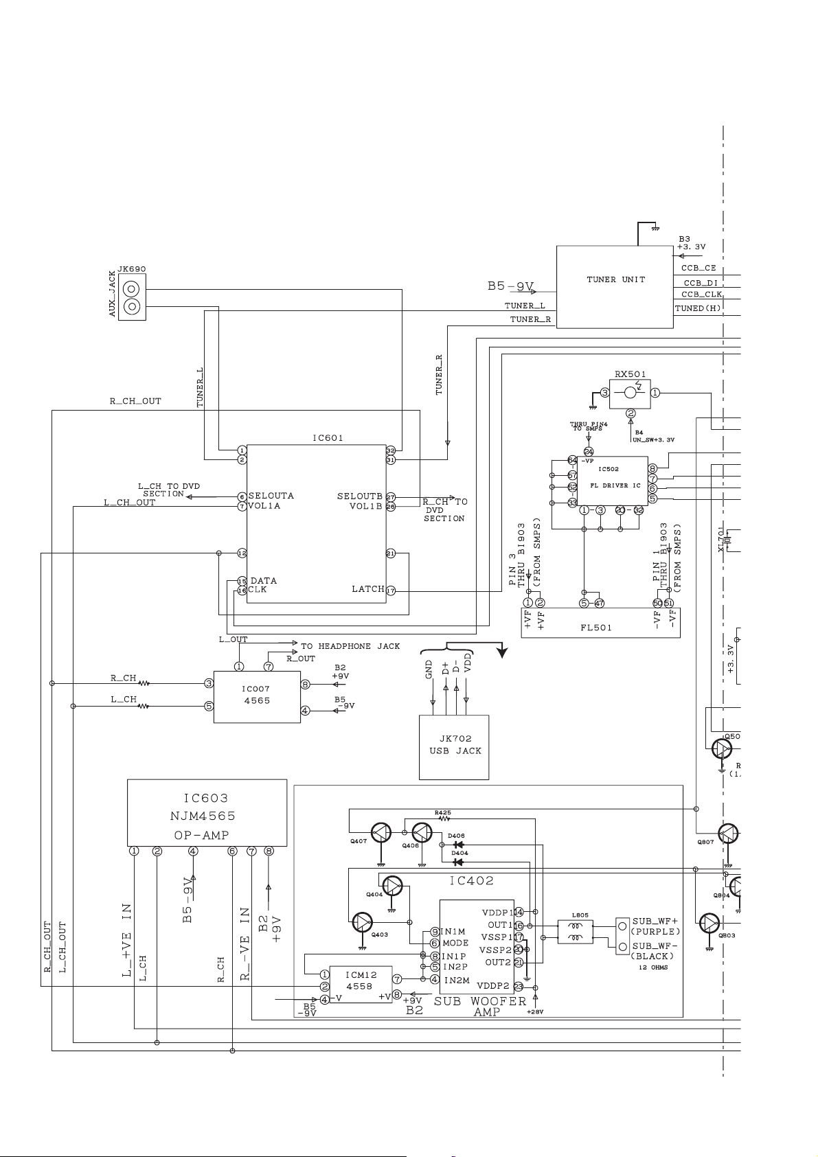
IC 402 IC 502
PINNOVOLTAGE
(V)
1 32.30 1 35.10 23 24.23 45 35.30
2 25.70 2 35.20 24 38.59 46 29.80
3 24.41 3 35.58 25 38.60 47 38.30
4 4.70 4 35.50 26 38.26 48 29.70
5 1.50 5 0.57 27 32.65 49 32.66
6 1.70 6 0.58 28 38.30 50 29.87
7 30.43 7 0.66 29 32.30 51 27.13
8 3.40 8 0.70 30 32.90 52 0.70
9 1.90 9 3.89 31 32.70 53 38.25
10 24.40 10 3.90 32 29.96 54 38.41
11 2.30 11 0.64 33 38.20 55 38.45
12 28.70 12 2.40 34 35.50 56 38.20
13 32.30 13 2.40 35 38.20 57 28.30
14 22.90 14 3.90 36 32.70 58 32.80
15 31.20 15 3.87 37 27.07 59 32.90
16 30.80 16 38.30 38 29.75 60 35.56
17 30.40 17 38.40 39 32.60 61 35.63
18 29.40 18 38.30 40 38.26 62 35.53
19 29.70 19 38.30 41 32.26 63 32.80
20 11.80 20 38.20 42 29.96 64 35.56
21 2.40 21 38.30 43 38.15
22 2.50 22 35.51 44 26.95
23 24.87
24 29.60
IC 601 IC 603
PINNOVOLTAGE
(V)
1 4.01 13 4.80m 1 1.47 4 -10.48
2 4.02 14 4.70m 2 1.43 5 1.28
3 4.01 15 3.15 3 1.43 6 1.27
4 4.03 16 3.15 4 -10.50 7 1.27
5 4.00 17 3.21 5 1.41 8 7.60
6 4.03 18 9.02 6 1.41
7 4.01 19 9.02 7 1.41
8 4.03 20 4.00 8 7.62
9 4.03 21 4.03
10 4.01 22 4.03
11 4.02 23 4.03
12 4.00 24 4.03 3 9.02
IC 802 312.00
(V)
1 27.40 13 19.43 2 0.50m
2 24.80m 14 27.30 3 3.32
3 27.10 15 12.12
4 52.30m 16 74.30m
5 52.20m 17 27.60
6 5.15 18 15.36
7 24.60m 19 27.40 1 1.47
8 52.50m 20 27.50 2 1.43
9 52.70m 21 21.40m 3 1.43
10 27.12 22 12.04 4 10.50
11
12 27.40 24 27.40
25.10m 23
PINNOVOLTAGE
(V)
PINNOVOLTAGE
(V)
PINNOVOLTAGE
(V)
27.36 5 1.41
PINNOVOLTAGE
(V)
PINNOVOLTAGE
(V)
IC 890
PINNOVOLTAGE
(V)
115.84
2 0.40m IC 892
PINNOVOLTAGE
IC 007
PINNOVOLTAGE
11.50
21.50
31.50
IC 891
PINNOVOLTAGE
115.84
2 0.20m
PINNOVOLTAGE
19.02
IC 703
PINNOVOLTAGE
(V)
(V)
(V)
(V)PINNOVOLTAGE
(V)
HT-DV40H
5 – 8
Page 28
HT-DV40H
IC 701
PINNOVOLTAGE
(V)
1 1.74 26 1.23 51 2.36 76 1.41
2 1.76 27 1.23 52 1.02 77 250.10m
3 0.94 28 1.24 53 0.99 78 226.50m
4 1.08 29 2.01 54 2.26 79 1.50
5 1.03 30 1.96 55 1.03 80 1.77
6 282.30m 31 1.19 56 1.05 81 1.99
7 0.94 32 1.18 57 1.07 82 1.90
8 0.94 33 1.18 58 258.50m 83 0.70
9 0.94 34 1.15 59 1.99 84 2.02
10 0.95 35 2.14 60 1.94 85 2.02
11 0.95 36 1.13 61 1.80 86 1.19
12 0.96 37 1.15 62 1.49 87 1.23
13 2.24 38 1.15 63 1.73 88 1.26
14 1.70 39 1.14 64 1.66 89 1.19
15 0.93 40 2.11 65 1.60 90 1.32
16 4.32 41 2.08 66 6.00 91 1.35
17 2.67 42 2.08 67 1.67 92 1.15
18 2.20 43 1.12 68 1.70 93 2.03
19 1.70 44 1.18 69 1.70 94 269.50m
20 1.53 45 2.16 70 1.40 95 89.50m
21 1.47 46 2.16 71 1.38 96 0.82
22 1.89 47 2.15 72 1.36 97 1.80
23 1.92 48 1.11 73 1.88 98 1.82
24 2.04 49 1.11 74 1.89 99 1.36
25 1.96 50 2.16 75 1.86 100 1.35
PINNOVOLTAGE
(V)
PINNOVOLTAGE
(V)
PINNOVOLTAGE
(V)
ICM 12 IC 903 IC 904 Q 406
PINNOVOLTAGE
(V)
1 6.50 1 16.30 1 16.30 1 5.00
2 1.90 2 5.20 2 3.40 2 3.70
3 2.57 3 0.60m 3 0.30m 3 3.40
4 -2.12 4 0.90 4 0.90
5 2.90 5 15.00 5 15.00
6 2.90
7 5.17
8 5.88
Q 602
PINNOVOLTAGE
(V)
1 1.04
2 0.74
3 0.80
Q 612
PINNOVOLTAGE
(V)
1 0.86
2 0.65
3 0.44
Q 613
PINNOVOLTAGE
(V)
1 0.79
2 0.79
3 0.47
PINNOVOLTAGE
(V)
Q 407 Q 506 Q 601
PINNOVOLTAGE
(V)
1 3.20 1 1.97 1 2.30
2 24.70m 2 3.80 2 2.30
3 3.20 3 3.96 3 2.30
Q 616 Q 702 Q 801
PINNOVOLTAGE
(V)
1 1.60 1 1.59 1 5.70
2 1.85 2 1.60 2 23.10m
3 1.65 3 1.58 3 5.50
Q 701 Q 802 Q 803
PINNOVOLTAGE
(V)
1
2 1.63 2 23.20m 2 4.60
3 1.57 3 5.17 3 23.40m
1.56 1 4.60 1
PINNOVOLTAGE
(V)
PINNOVOLTAGE
(V)
PINNOVOLTAGE
(V)
PINNOVOLTAGE
(V)
PINNOVOLTAGE
PINNOVOLTAGE
PINNOVOLTAGE
PINNOVOLTAGE
2.70m
(V)
(V)
(V)
(V)
5 – 9
Page 29
Q 804 Q 806 Q 807 QM 7
PINNOVOLTAGE
(V)
1 2.70m 1 1.97 1 1.93 1 1.90
2 5.40 2 1.97 2 1.37 2 2.90m
3 23.40m 3 7.00 3 1.30 3 3.00m
QM 8 QM 9 QM 16 QM 17
PINNOVOLTAGE
(V)
1 3.40 1 2.68 1 8.55 1 0.76
2 8.40 2 8.50 2 4.19 2 0.70
3 3.40 3 2.70 3 8.62 3 0.70
QM 23 Q 013 Q 014
(V)
1 0.73 1 2.70 1 2.70 21.03
2 0.74 2 1.50 2 1.58 32.80
3 0.74 3 1.60 3 1.67 40.01
PC 901 IC 901 IC 902
PINNOVOLTAGE
(V)
1 25.56 1 2.47 1 3.87
2 24.46 2 0.00 2 0.00 Q 906
3 2.14 3 24.46 3 8.08
4 12.33
Q 901
PINNOVOLTAGE
(V)
E -9.15 C -59.5 C 0.58 Q 908
C -17.03 B -34.9 B 0.74
B -9.77
PINNOVOLTAGE
(V)
PINNOVOLTAGE
(V)
4 8.50 4 3.60
PINNOVOLTAGE
(V)
PINNOVOLTAGE
(V)
Q 901 Q 904 G 356.70
PINNOVOLTAGE
(V)
E -34.3 E 0.00
PINNOVOLTAGE
(V)
PINNOVOLTAGE
(V)
PINNOVOLTAGE
(V)
PINNOVOLTAGE
(V)
VOLTAGE
PIN
NO
(V)
PINNOVOLTAGE
PINNOVOLTAGE
PINNOVOLTAGE
10.39
50.00
6 12.44
71.14
80.35
PINNOVOLTAGE
D0.00
S0
PINNOVOLTAGE
E0.00
C 3.32
B0.00
IC 900
(V)
(V)
(V)PINNOVOLTAGE
(V)
0
.0
(V)
HT-DV40H
5 – 10
Page 30

HT-DV40H
-MEMO-
5 – 11
Page 31

AudioCD-DV650WService ManualCD-DV650WMarketE
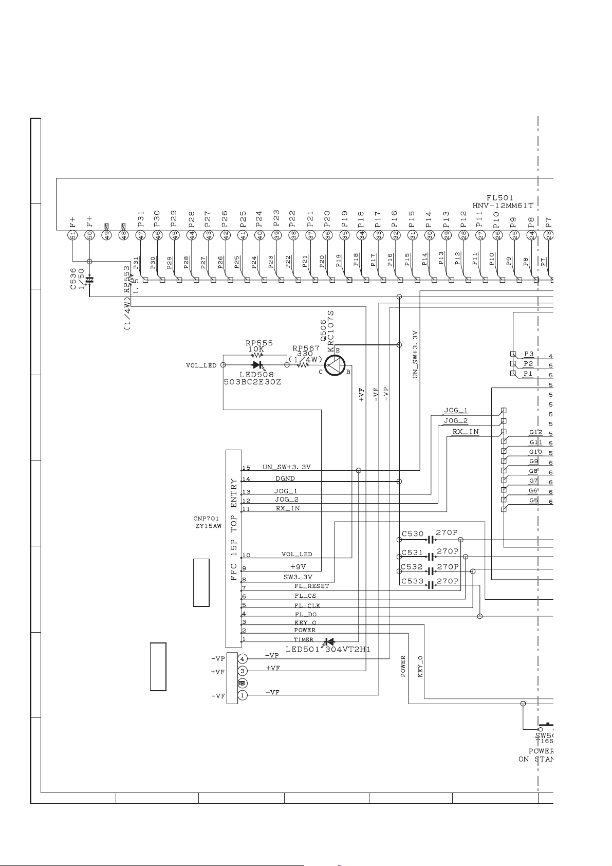
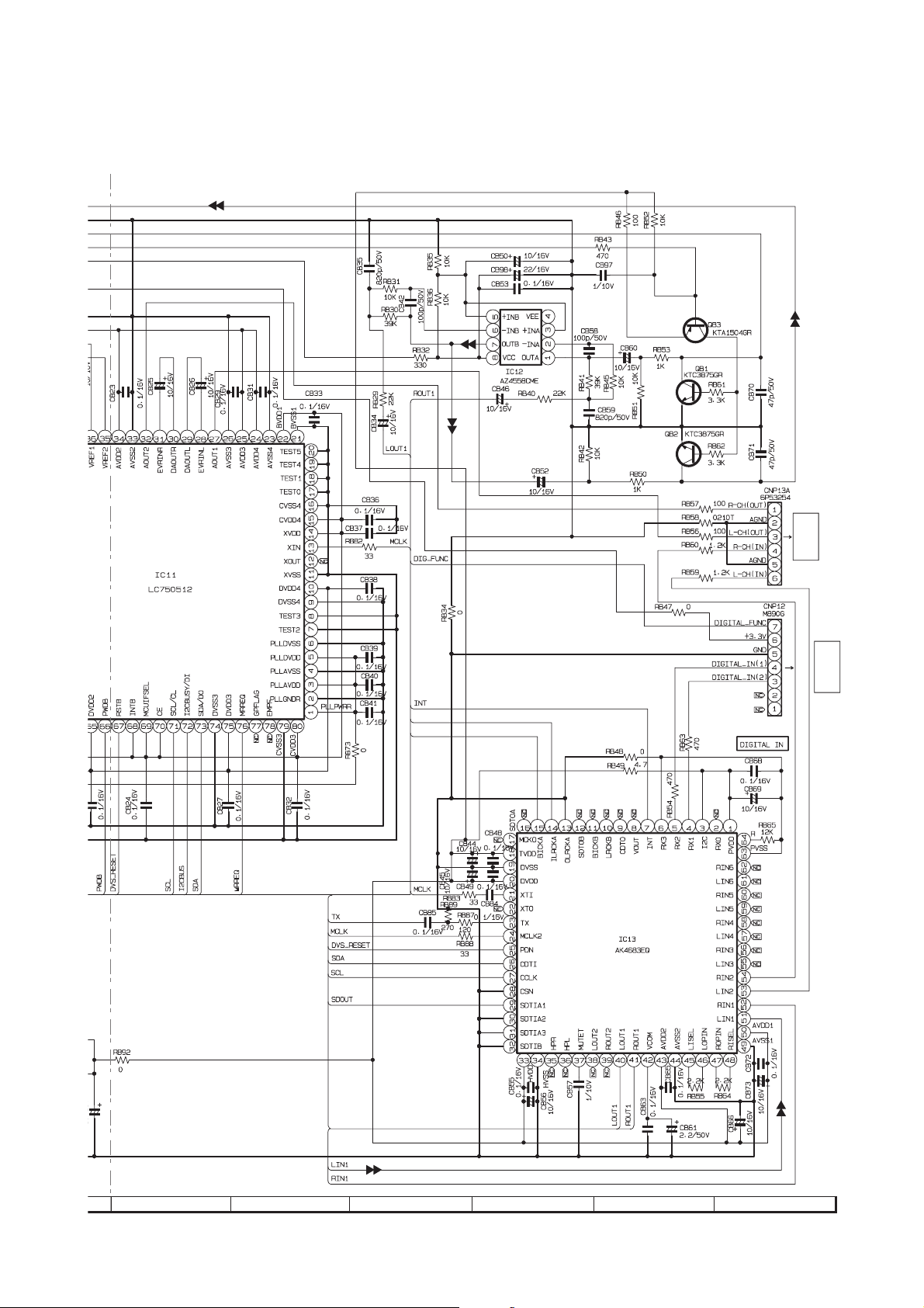
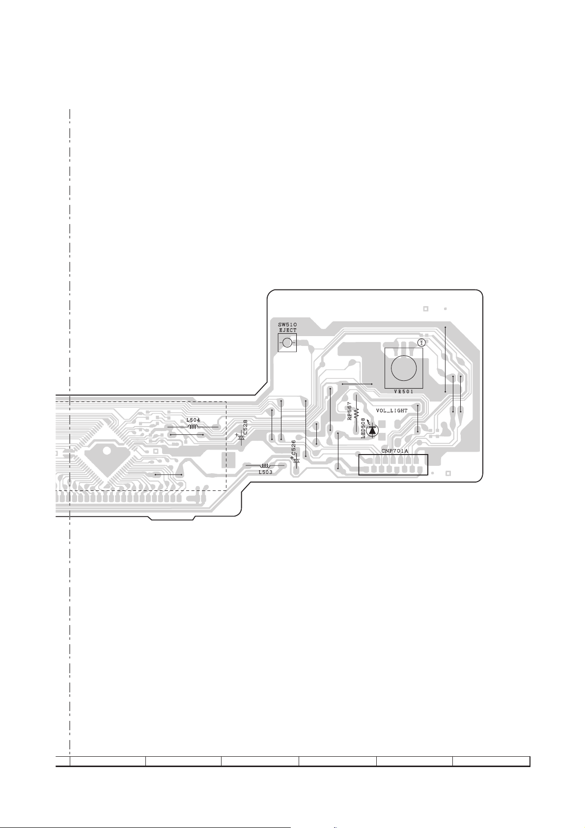
CHAPTER 6. CIRCUIT SCHEMATICS AND PARTS LAYOUT
[1] Notes On Schematic Diagram
• Resistor:
To differentiate the units of resistors, such symbol as K
and M are used: the symbol K means 1000 ohm and the
symbol M means 1000 kohm and the resistor without any
symbol is ohm-type resistor. Besides, the one with “Fusible” is a fuse type.
• Capacitor:
To indicate the unit of capacitor, a symbol P is used: this
symbol P means pico-farad and the unit of the capacitor
without such a symbol is microfarad. As to electrolytic
capacitor, the expression “capacitance/withstand voltage”
is used.
(CH), (TH), (RH), (UJ): Temperature compensation
(ML): Mylar type
(P.P.): Polypropylene type
REF. NO DESCRIPTION POSITION
SW501 POWER ON/STANDBY ON—OFF
SW507 DVD/CD/USB PLAY/PAUSE ON—OFF
SW508 DISC/USB STOP ON—OFF
SW509 FUNCTION ON—OFF
SW510 DISC OPEN/CLOSE ON—OFF
VR501 VOLUME MIN—MAX
• Schematic diagram and Wiring Side of P.W.Board for this
model are subject to change for improvement without
prior notice.
• The indicated voltage in each section is the one measured
by Digital Multimeter between such a section and the
chassis with no signal given.
1. In the tuner section,
indicates FM stereo
2. In the main section, DVD is being played back.
3. In the power section, DVD is being played back.
4. In the DVD section, the DVD is stopped.
• Parts marked with “ “ ( ) are important
for maintaining the safety of the set. Be sure to replace
these parts with specified ones for maintaining the safety
and performance of the set.
HT-DV40H
[2] Types Of Transistor And LED
FRONT
VIEW
E C B
(S)(G)(D)
(1)(2)(3)
KIA78L05
KT A1023 Y
KIA431 A
B
(3)
TOP
VIEW
E
(1)
KRA107 S
KRC102 S
KRC104 S
KRC107 S
KTA1504 GR
KTC3875 GR
KTK5133 S
KTC2875 B
SK536
KT A1298 Y
SC3928 AR
KDS226
C
(2)
FRONT
VIEW
1 2 3
KIA7809
KIA7812
STTH1002CFP
06N80C3
TOP VIEW
BCE
2SA2012
KTC4375Y
FRONT
VIEW
304VT2H
503BC2E
HSS4148
1N4004
FH3+++
MA111
FRONT VIEW
+ AC AC
D10XB60F
6 – 1
Page 32

HT-DV40H
[3] Schematic Diagram
A
B
AUDIO SIGNAL
FM SIGNAL
C
TO DISPLAY PWB-B2
TO DVD PWB-C
D
E
F
MIC_IN
G
H
1
23456
Figure 6-1: MAIN SCHEMATIC DIAGRAM (1/8)
6 – 2
Page 33

B2
HT-DV40H
TO
DVD PWB-C
(CNP14)
4700pF/50V
4700pF/
50V
7
8 9 10 11 12
Figure 6-2: MAIN SCHEMATIC DIAGRAM (2/8)
6 – 3
Page 34

HT-DV40H
SUBWOOFER PWB-D
TO
(BI402)
13
14 15 16 17 18
Figure 6-3: MAIN SCHEMATIC DIAGRAM (3/8)
6 – 4
Page 35

HT-DV40H
MIC_IN
A
B
C
D
E
F
G
H
1
23456
Figure 6-4: MAIN SCHEMATIC DIAGRAM (4/8)
6 – 5
Page 36
HT-DV40H
AZ4558CME
JP826
7
8 9 10 11 12
Figure 6-5: MAIN SCHEMATIC DIAGRAM (5/8)
6 – 6
Page 37

HT-DV40H
ME
C634
0.047/50V
D605
MA111G
D606
MA111G
13
14 15 16 17 18
Figure 6-6: MAIN SCHEMATIC DIAGRAM (6/8)
6 – 7
Page 38

HT-DV40H
A
B
AUDIO SIGNAL
C
D
E
F
G
H
1
23456
Figure 6-7: MAIN SCHEMATIC DIAGRAM (7/8)
6 – 8
Page 39

HT-DV40H
SPEAKER TERMINAL
7
8 9 10 11 12
Figure 6-8: MAIN SCHEMATIC DIAGRAM (8/8)
6 – 9
Page 40

HT-DV40H
A
B
C
D
E
F
BI706
G
H
1
23456
Figure 6-9: USB SCHEMATIC DIAGRAM
6 – 10
Page 41

-MEMO-
HT-DV40H
6 – 11
Page 42

HT-DV40H
C
A
B
C
D
E
F
1.5K
1
G
BLUE
AC SUPPLY
AC 220-240 V ~ 50Hz
H
1
23456
Figure 6-10: POWER SCHEMATIC DIAGRAM (1/2)
6 – 12
Page 43
HT-DV40H
101P
C999
L912
F0015
R973
FB
FB
FB
HEADPHONE JACK
7
8 9 10 11 12
Figure 6-11: POWER SCHEMATIC DIAGRAM (2/2)
6 – 13
Page 44
HT-DV40H
A
B
C
D
E
F
CNP701B
TO MAIN PWB-A
Bi502
A691AW
G
CNP903
TO POWER PWB-B1
H
1
23456
Figure 6-12: DISPLAY SCHEMATIC DIAGRAM (1/2)
6 – 14
Page 45

HT-DV40H
7
8 9 10 11 12
Figure 6-13: DISPLAY SCHEMATIC DIAGRAM (2/2)
6 – 15
Page 46

HT-DV40H
A
B
VIDEO SIGNAL
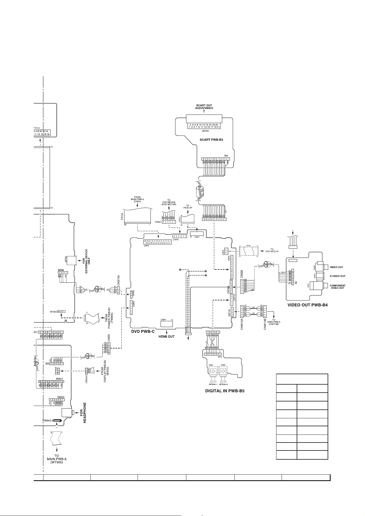
CD SIGNAL
SCART PWB-B3
Bi9
1000P
DIGITAL-IN PWB-B5
1000P
C
D
E
F
TO DVD PWB-C
FROM DVD PWB-C
VIDEO OUT PWB-B4
0.47uH
FROM DVD PWB-C
G
FROM DVD PWB-C
H
1
23456
Figure 6-14: SCART, DIGITAL IN & VIDEO OUT SCHEMATIC DIAGRAM
6 – 16
Page 47

-MEMO-
HT-DV40H
6 – 17
Page 48

HT-DV40H
A
B
C
D
E
TO
F
MOTOR
DVD MECHA
5
G
2
1
H
1
23456
Figure 6-15: DVD SCHEMATIC DIAGRAM (1/8)
6 – 18
Page 49

HT-DV40H
7
8 9 10 11 12
Figure 6-16: DVD SCHEMATIC DIAGRAM (2/8)
6 – 19
Page 50

HT-DV40H
CD SIGNAL
VIDEO SIGNAL
13
TO SCART PWB-B3
14 15 16 17 18
OUT PWB-B4
Figure 6-17: DVD SCHEMATIC DIAGRAM (3/8)
6 – 20
Page 51

HT-DV40H
T
M
O
M
DVD
2
A
1
B
4
3
C
TO MAIN PWB-A
(CNS4)
D
E
(Bi5)
TO POWER PWB-B1
F
G
H
1
23456
Figure 6-18: DVD SCHEMATIC DIAGRAM (4/8)
6 – 21
Page 52

HT-DV40H
7
8 9 10 11 12
Figure 6-19: DVD SCHEMATIC DIAGRAM (5/8)
6 – 22
Page 53

HT-DV40H
TO SCART PWB-B3
6
TO VIDEO OUT PWB-B4
7
13
(Bi706)
TO MAIN PWB-A
The number to are waveform number shown in page 7-3
1 7
14 15 16 17 18
Figure 6-20: DVD SCHEMATIC DIAGRAM (6/8)
6 – 23
Page 54

HT-DV40H
A
B
C
CD SIGNAL
D
E
F
G
H
1
23456
Figure 6-21: DVD SCHEMATIC DIAGRAM (7/8)
6 – 24
Page 55
HT-DV40H
ILRCKA
BICKA
PWB-A
TO MAIN
IN PWB-B5
TO DIGITAL
7
8 9 10 11 12
Figure 6-22: DVD SCHEMATIC DIAGRAM (8/8)
6 – 25
Page 56

HT-DV40H
A
B
C
FROM
MAIN PWB-A
(BI402)
D
E
F
G
H
1
23456
Figure 6-23: SUBWOOFER SCHEMATIC DIAGRAM (1/2)
6 – 26
Page 57

AUDIO SIGNAL
HT-DV40H
SUBWOOFER
SPEAKER OUTPUT
TO MAIN PWB-A
CNP801
7
8 9 10 11 12
Figure 6-24: SUBWOOFER SCHEMATIC DIAGRAM (2/2)
6 – 27
Page 58

HT-DV40H
K
[4] Charts Of Connecting Wires
A
B
C
RF4
RING CORE
(1 TURN)
RF3
(2 TURN)
RING CORE
(TP1)
CNP901
D
23
E
FROM
(Bi403)
SUBWOOFER PWB-C
F
RING CORE
(1 TURN)
RF2
RF1
(1 TURN)
SILINDER CORE
G
BR
BL
J
H
1
23456
Figure 6-25: WIRING CONNECTION (1/2)
6 – 28
Page 59
RF8
(1 TURN)
SILINDER CORE
HT-DV40H
JK900
RF6
RING CORE
(2 TURN)
(USB TERMINAL)
RF5
RING CORE
(2 TURN)
BL
CNS201
TO
VIDEO OUT PWB-B4
(CNP201)
CNS9
FROM
DVD PWB-C
BL
BK
RD
GR
1234
CNS201
1234
CNP201
GR
BK
RD
CNS12
RF7
RING CORE
(2 TURN)
COLOR TABLE
RD
BK
GY
YL
BR
GR
PK
WH
BL
RED
BLACK
GREY
YELLOW
BROWN
GREEN
PINK
WHITE
BLUE
7
8 9 10 11 12
Figure 6-26: WIRING CONNECTION (2/2)
6 – 29
Page 60

HT-DV40H
7
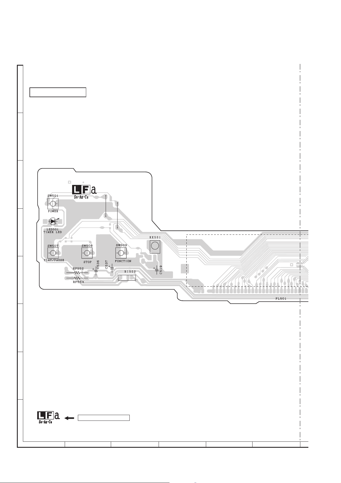
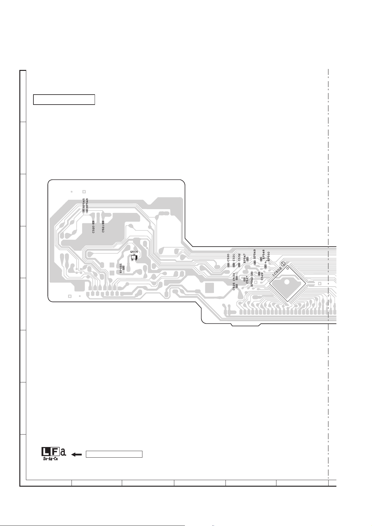
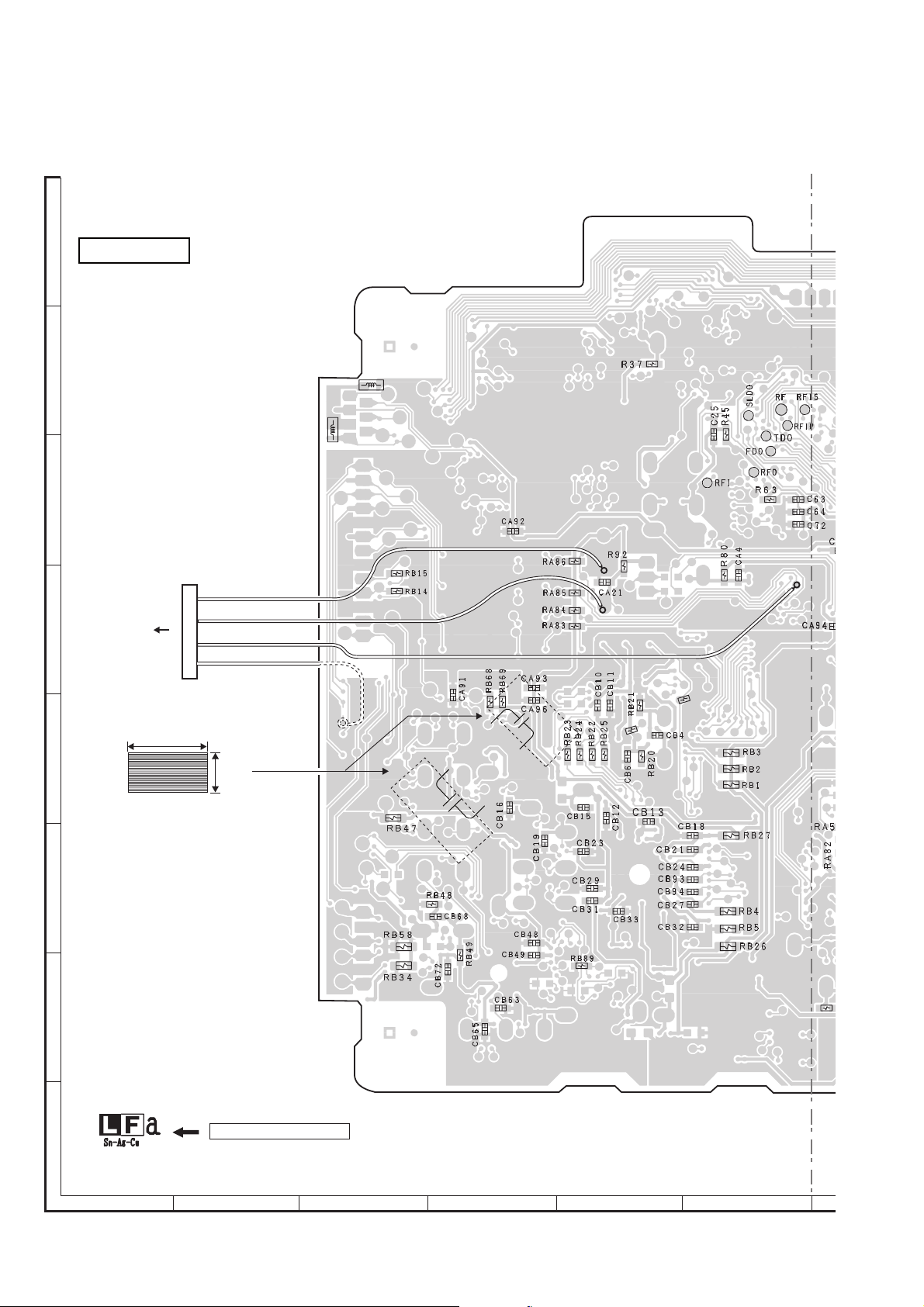
[5] Wiring Side Of PWB
A
MAIN PWB-A
B
C
D
E
F
MICOM REFLASH
FRONT
SPEAKERS
TERMINAL
FOR
ONLY
AUX
IN
R-CH
L-CH
45
123
15
12 3456 78
123
WIR1 (BL)
WIR3 (BL)
654321
891011
1
25
G
Lead-free solder indication
H
Lead-free solder is used in the MAIN PWB.
Refer to "Precautions for handling lead-free solder" for instructions
and precautions.
1
23456
Figure 6-27: WIRING SIDE OF MAIN PWB (TOP VIEW) (1/2)
6 – 30
Page 61

HT-DV40H
WIR2 (BL)
1
564321
12345
6
7891011
15
BCE
FROM
USB EXTERNAL
DEVICE
12345
ECB
COLOR TABLE
BL BLUE
7
8 9 10 11 12
Figure 6-28: WIRING SIDE OF MAIN PWB (TOP VIEW) (2/2)
6 – 31
Page 62

HT-DV40H
A
MAIN PWB-A
B
C
WIR 4
D
E
F
G
Lead-free solder indication
H
Lead-free solder is used in the MAIN PWB.
Refer to "Precautions for handling lead-free solder" for instructions
and precautions.
1
23456
Figure 6-29: WIRING SIDE OF MAIN PWB (BOTTOM VIEW) (1/2)
6 – 32
Page 63

(BL)
HT-DV40H
WIR 5
(GY)
COLOR TABLE
BLUE
GYBLGREY
7
8 9 10 11 12
Figure 6-30: WIRING SIDE OF MAIN PWB (BOTTOM VIEW) (2/2)
6 – 33
Page 64

HT-DV40H
A
POWER PWB-B1
B
C
D
AC POWER SUPPLY
CORD (233)
AC 220-240V~50Hz
E
F
G
BL
BR
ECB
1
2
3
4
5
6
7
8
9
Lead-free solder indication
H
Lead-free solder is used in the POWER PWB.
Refer to "Precautions for handling lead-free solder" for instructions
and precautions.
1
23456
Figure 6-31: WIRING SIDE OF POWER PWB (TOP VIEW) (1/2)
6 – 34
Page 65

HT-DV40H
1
NC
2
3
4
1
2
3
4
5
6
7
8
NC
9
9
8
7
6
5
18
17
16
15
14
13
12
11
10
ECB
ECB
1
2
3
1234567
ECB
11128910
765
321
1234
ECB
1234567
FROM
1
2
3
HEADPHONE
COLOR TABLE
BROWN
BLBRBLUE
7
8 9 10 11 12
Figure 6-32: WIRING SIDE OF POWER PWB (TOP VIEW) (2/2)
6 – 35
Page 66

HT-DV40H
A
POWER PWB-B1
B
C
D
E
F
G
Lead-free solder indication
H
Lead-free solder is used in the POWER PWB.
Refer to "Precautions for handling lead-free solder" for instructions
and precautions.
1
23456
Figure 6-33: WIRING SIDE OF POWER PWB (BOTTOM VIEW) (1/2)
6 – 36
Page 67

HT-DV40H
7
8 9 10 11 12
Figure 6-34: WIRING SIDE OF POWER PWB (BOTTOM VIEW) (2/2)
6 – 37
Page 68
HT-DV40H
A
DISPLAY PWB-B2
B
C
D
E
1234
123456789
10 111213 14 15 16 17 18 19202122232425 2627 28 303129
F
G
Lead-free solder indication
H
Lead-free solder is used in the DISPLAY PWB.
Refer to "Precautions for handling lead-free solder" for instructions
and precautions.
1
23456
Figure 6-35: WIRING SIDE OF DISPLAY PWB (TOP VIEW) (1/2)
6 – 38
Page 69
HT-DV40H
728 3031323334353637383940414243444546474849505129
2 4 6 8 10 12 14
13579111315
7
8 9 10 11 12
Figure 6-36: WIRING SIDE OF DISPLAY PWB (TOP VIEW) (2/2)
6 – 39
Page 70
HT-DV40H
A
DISPLAY PWB-B2
B
C
D
E
F
G
Lead-free solder indication
H
Lead-free solder is used in the DISPLAY PWB.
Refer to "Precautions for handling lead-free solder" for instructions
and precautions.
1
23456
Figure 6-37: WIRING SIDE OF DISPLAY PWB (BOTTOM VIEW) (1/2)
6 – 40
Page 71

HT-DV40H
7
8 9 10 11 12
Figure 6-38: WIRING SIDE OF DISPLAY PWB (BOTTOM VIEW) (2/2)
6 – 41
Page 72

HT-DV40H
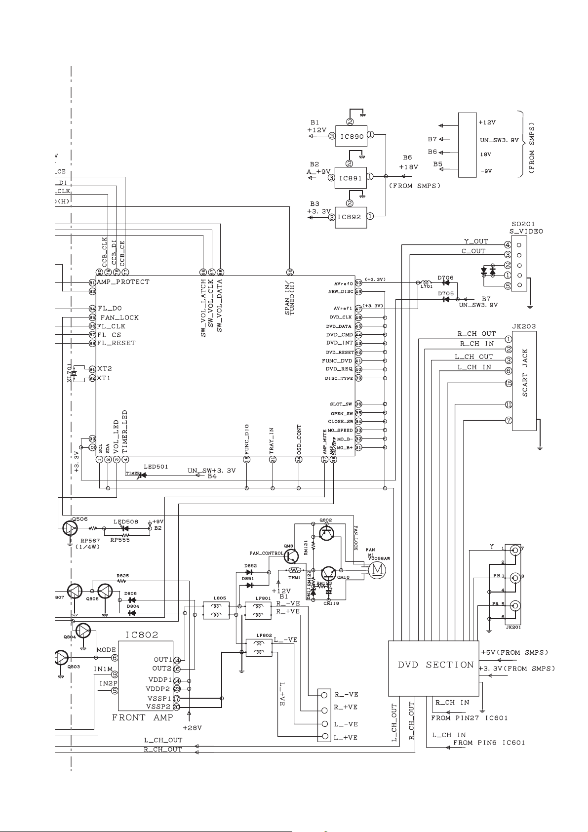
SCART PWB-B3
A
6987
15114213312411510
B
C
13579111315171921
2468101214161820
SCART OUT
AUDIO/VIDEO
D
VIDEO OUT PWB-B4 DIGITAL IN PWB-B5
VIDEO
OUT
S-VIDEO
COMPONENT
OUT
OUT
E
F
123456789
G
Lead-free solder indication
Lead-free solder is used in the SCART, VIDEO OUT, DIGITAL IN PWB.
Refer to "Precautions for handling lead-free solder" for instructions
H
and precautions.
OPTICAL-1
OPTICAL-2
23456789
1
1
23456
Figure 6-39: WIRING SIDE OF SCART, VIDEO OUT, DIGITAL IN PWB (TOP VIEW)
6 – 42
Page 73

HT-DV40H
SCART PWB-B3
A
B
C
D
VIDEO OUT PWB-B4 DIGITAL IN PWB-B5
E
F
G
Lead-free solder indication
Lead-free solder is used in the SCART, VIDEO OUT, DIGITAL IN PWB.
Refer to "Precautions for handling lead-free solder" for instructions
H
and precautions.
1
Figure 6-40: WIRING SIDE OF SCART, VIDEO OUT, DIGITAL IN PWB (BOTTOM VIEW)
23456
6 – 43
Page 74

HT-DV40H
A
DVD PWB-C
B
C
25
24
23
22
21
1315
1719
1012
1416
1820
13245768911
123456
D
E
1234
F
4365 21
G
Lead-free solder indication
H
Lead-free solder is used in the DVD PWB.
Refer to "Precautions for handling lead-free solder" for instructions
and precautions.
1
23456
Figure 6-41: WIRING SIDE OF DVD PWB (TOP VIEW) (1/2)
HDMI OUT
6 – 44
Page 75

HT-DV40H
24 1
1
642
7531
4321876512 11 10 913
RD
CNS201
GR
BK
BL
RD
TO
(CNP201)
VIDEO OUT PWB-B4
12345678
234567
1
123456
COLOR TABLE
GR GREEN
BK BLACK
BL BLUE
RD RED
7
8 9 10 11 12
Figure 6-42: WIRING SIDE OF DVD PWB (TOP VIEW) (2/2)
6 – 45
Page 76
HT-DV40H
A
DVD PWB-C
B
RC3
RB1
C
GR
CNS201
GR
BK
D
E
TO
(CNP201)
VIDEO OUT PWB-B4
Filament tape
20mm
BL
RD
10mm
CB97
CB98
BK
RB95
RB94
BL
F
G
Lead-free solder indication
H
Lead-free solder is used in the DVD PWB.
Refer to "Precautions for handling lead-free solder" for instructions
and precautions.
1
23456
Figure 6-43: WIRING SIDE OF DVD PWB (BOTTOM VIEW) (1/2)
6 – 46
Page 77

CC3
HT-DV40H
COPPER FOIL
PSH3
CR1
20mm
10mm
Filament tape
BL
WIR 6
COLOR TABLE
GR GREEN
BK BLACK
BL BLUE
RD RED
7
8 9 10 11 12
Figure 6-44: WIRING SIDE OF DVD PWB (BOTTOM VIEW) (2/2)
6 – 47
Page 78

HT-DV40H
4
4
4
A
SUBWOOFER PWB-D
BI403
12345678
C402
B
C405
LF402LF401
L402
C
D
+
C401
R405
R
R
+
JK404
JF3
C406
C
SUBWOOFER
TERMINAL
E
-
C409
F
C451
G
Lead-free solder indication
H
Lead-free solder is used in the
Refer to "Precautions for handling lead-free solder" for instructions
and precautions.
1
SUBWOOFER
23456
Figure 6-45: WIRING SIDE OF SUBWOOFER PWB (TOP VIEW) (1/2)
PWB.
R452
C449
6 – 48
C456
R414
C457
Page 79

HT-DV40H
R420
R421
L401
R401
R402
C435
1
C404
C434
C420
C419
IC402
C428
C418
C412
C433
C417
C413
R419
R417
R403 R404
BI402
Q402
R416
87645321
Q403
Q404
R418
Q401
C429
C430
C403
C431
C422
C467
R411
R412
94V-0
C438
C415
C407
L405
7
8 9 10 11 12
Figure 6-46: WIRING SIDE OF SUBWOOFER PWB (TOP VIEW) (2/2)
6 – 49
Page 80

HT-DV40H
A
SUBWOOFER PWB-D
B
R429
R408
R410
DZ401
J1
C445
R415
C423
C
C409
R406
C446
D406
D405
R423
Q407
R427
C465
R422
R425
C440
C452
R413
C453
D
Q406
C464
D404
E
D403
R424
C463
C427
C411
C421
C436
C410
C454
R407
C455
F
C441
G
Lead-free solder indication
H
Lead-free solder is used in the
Refer to "Precautions for handling lead-free solder" for instructions
and precautions.
1
SUBWOOFER
PWB.
23456
Figure 6-47: WIRING SIDE OF SUBWOOFER PWB (BOTTOM VIEW) (1/2)
6 – 50
Page 81

C425
HT-DV40H
C461
C462
C424
C432
D402
JF4
R451
C460
JF2
C439
Q405
D401
C442
R440
C447
C448
R441
D451
7
8 9 10 11 12
Figure 6-48: WIRING SIDE OF SUBWOOFER PWB (BOTTOM VIEW) (2/2)
6 – 51
Page 82

HT-DV40H
CHAPTER 7. FLOWCHART
[1] Troubleshooting
1. When the CD/DVD does not function
The CD/DVD section may not operate when the objective lens of the optical pickup is dirty. Clean the objective lens,
and check the playback operation. When this section does not operate even after the above step is taken, check the
following items.
Remove the cabinet and follow the trouble shooting instructions.
"Track skipping and/or no TOC (Table Of Contents) may be caused by build up of dust or other foreign matter on the
laser pickup lens. Before attempting any adjustment make certain that the lens is clean. If not, clean it as mentioned
below."
Turn the power off.
Gently clean the lens with a lens cleaning tissue and a small amount of isopropyl alcohol.
Do not touch the lens with the bare hand.
Parts code
1. CD optical pickup Lens cleaner disc UDSKA0004AFZZ
HOW TO USE
Using the brush in the cleaner cap, apply 1 or 2 drops of the cleaning fluid to the
1.
brush on the CD cleaner disc which has the mark next to it.
Place the CD cleaner disc onto the CD/DVD disc tray with the brush side down,
2.
then press the play button.
You will hear music for about 20 seconds and the CD/DVD player will automatically
3.
stop. If it still play continuously, press the stop button.
Cleaning fluid
CAUTION
The CD lens cleaner should be effective for 30-50 operations, however if the
brushes become worn out earlier then please replace the cleaner disc.
If the CD cleaner brushes become very wet then wipe off any excess fluid with a soft
cloth.
Do not drink the cleaner fluid or allow it contact with the eyes. In the event of this
happening then drink and/or rinse with clean water and seek medical advice.
The CD cleaner disc must not be used on car CD players or on computer CD-ROM
drives.
All rights reserved. Unauthorized duplicating, broadcasting and renting this product
is prohibited by law.
Cleaner disc
2. DVD Section
• “No Disc” is displayed. (Focus error)
Does the objective lens move up and down after the disc is
removed? (Check the following items.)
Yes
Is signal input to pins 4 - 11, 14, 15 of IC1? No Check connection of optical pickup cables.
No Check CNP1 pin 23, 24 and IC2 pin 13, 14.
If no abnormality is detected, replace optical pickup.
Is focus control signal output from pin 43 of IC1 to pin 1 of IC2? No Check focus control signal line between IC1 and IC2.
To 7-2 Page
(Refer Figure 1)
7 – 1
Page 83

From 7-1 Page
Yes
Is SLED control signal output from pin 58 of IC1 to pin 23 of IC2?
Yes
Is SPIN control signal output from pin 57 of IC1 to pin 4 of IC2?
Yes
Is Tracking control signal output from pin 42 of IC1 to pin 26
of IC2?
Yes
Is focus control drive voltage output from pins 13 and 14 of IC2? No Is voltage of 5 V applied to pin 8, 19 of IC2.
Yes
Is focus control drive voltage applied to the focus actuator
terminal? (Pin 23 and 24 of IC1)
No
No
No
No Check line between IC2 and focus actuator terminal.
Check SLED control signal line between IC1 and IC2
(Refer Figure 1)
Check SPIN control signal line between IC1 and IC2
(Refer Figure 1)
Check Tracking control signal line between IC1 and IC2
(Refer Figure 1)
HT-DV40H
Yes
Check connection of optical pickup cables.
If no abnormality is detected, replace the optical pickup
mechanism unit.
• “No Disc” is displayed during DVD playback (when CD is playable) ... When DVD laser does not light up.
Is control signal output from pin 18 of IC1? No Check signal line between IC1 and Q9.
Yes
Is voltage of 3.3V applied to emitter of Q9? No Check 3.3V line.
Yes
Is voltage of approx. 2.3 V supplied to pin 2 of CNP1? No
Yes
Check connection of optical pickup cables.
If no abnormality is detected, replace optical pickup mechanism
unit.
Check around Q9.
Note: The laser diode is easily damaged by static electricity.
Carefully check static electricity and electric leak of the measuring
instrument.
• “No Disc” is displayed during CD playback (when DVD is playable) ... When CD laser does not light up.
Is control signal output from pin 19 of IC1? Check signal line between IC1 and Q3.
Yes
Is voltage of 3.3V applied to the emitter of Q3? Check 3.3V line.
Yes
Is voltage of approx. 1.9 V supplied to pin 6 of CNP1? Check around Q3.
Yes
Check connection of optical pickup cables.
If no abnormality is detected, replace optical pickup mechanism
unit.
No
No
No
Note: The laser diode is easily damaged by static electricity.
Carefully check static electricity and electric leak of the measuring
instrument.
7 – 2
Page 84

HT-DV40H
3. Both Video and Audio do not operate normally
The RF waveform is normal and the time is displayed normally, but no sound is produced. Or the sound has dropouts.
1. Insert disc into DISC loader.
Yes
2. When playback starts does the disc initialise ? No Repeat steps as Focus Errror system check occurred.
Yes
3. Is the RF signal level output from IC1 pin no 252 normal?
( Waveform drawing Figure 3 for CD and Figure 2 for DVD )
Yes
4. Replace Servo PWB. No Replace optical pickup mechanism unit.
Yes
No Is the objective lens of optical pickups clean ?
Yes
5. Does the supply shows as +1.8V / + 3.3 V / + 5 V / + 12V? No Check supply ( IC3 Pin No. , +1.8V / CNP5 Pin 1, +3.3V /
CNP5 Pin 3, +5V / CNP5, +12V
Yes
6. Is Reset function OK? No Check CNP4 pin no 18 .
Yes
7. Is clock frequency shows 27MHz? No Check clock circuit ( XL1 , C86 , C92 )
Yes
8. Is the SDRAM is normal? No Check IC4 pin no 38 .
Yes
9. Is the DSP is normal? No Check IC1 Data Bus .
Yes
10. Is the Audio out is normal? No Check Audio out circuit ( CNP13A Pin No.1 and 3 )
Yes
11. Is the Video out is normal? No
IC1
1
43
Check Video out circuit ( IC1 Pin No.211, 218, 219 and 221 )
IC1
3
4
IC1
2
42
58
57
5
252
Figure 2
IC6
Figure 1
6
2
5
252
7
9
Figure 3
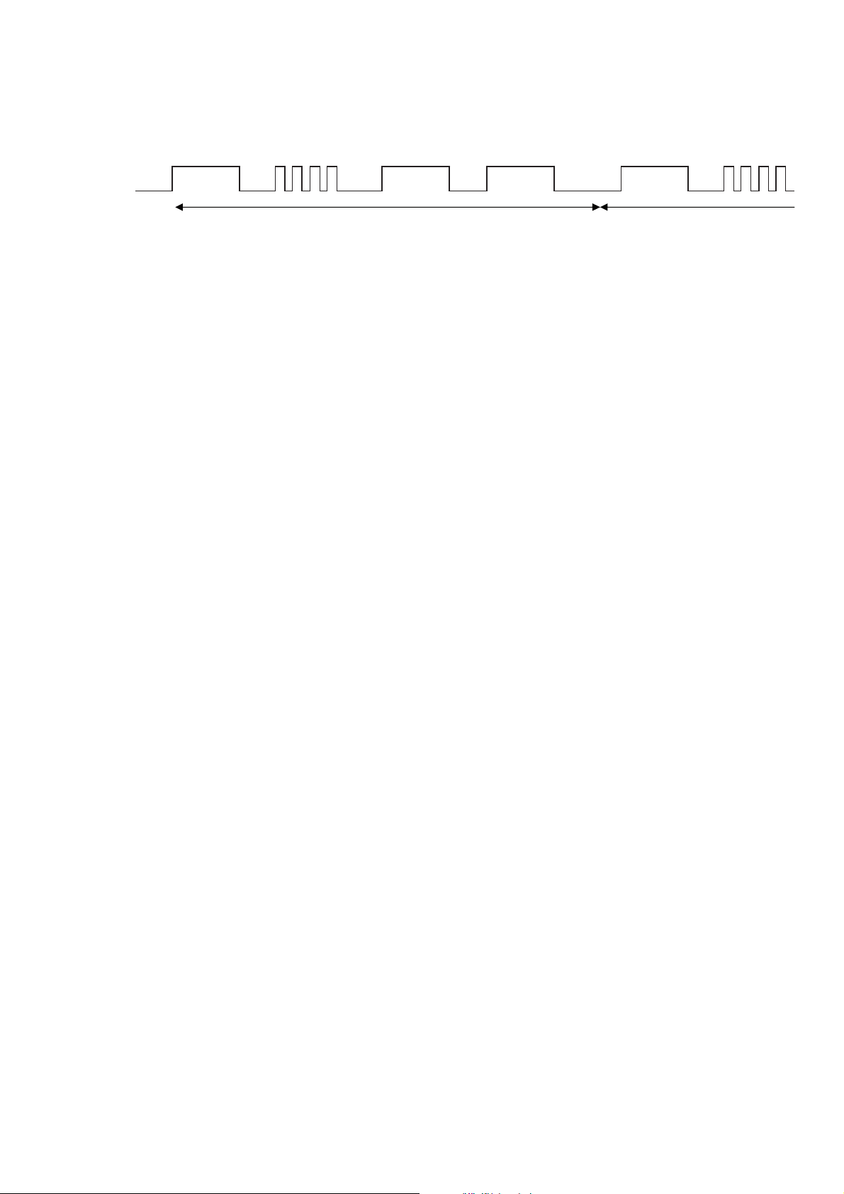
Figure 4
7 – 3
Page 85

4. Video is not output normally
Put a disc on the DISC tray.
Yes
HT-DV40H
Are the video signals input to the pins of CNP8 as shown below?
CNP8 Pin1 Composite
CNP8 Pin2 VGND
CNP8 Pin3 C
CNP8 Pin4 Py
CNP8 Pin5 VGND
CNP8 Pin6 Y
CNP8 Pin7 Pb
CNP8 Pin8 Pr
5. Audio is not output normally
Put a disc on the DISC tray.
Yes
Digital sound signal output from Pin 196, 198, 199, 201, 203
and 204 of IC1?
6. HDMi Video has no output.
No
No
Check the line between video out section and pins of CNP8
and CNP9.
Q11 to CNP8 Pin 8 (Pr) and Pin3 (C)
Q12 to CNP8 Pin 7 (Pb)
Q13 to CNP8 Pin 6 (Y)
Q14 to CNP8 Pin 1 (Composite)
Q11 to CNP9 Pin 4 (R)
Q12 to CNP9 Pin 3 (B)
Q13 to CNP9 Pin 2 (G)
Q14 to CNP9 Pin 1 (Composite)
Check each line between IC1, IC6 and IC10.
Pin 196 of IC1 to Pin 8 of IC6 and Pin 46 of IC10.
Pin 198 of IC1 to Pin 7 of IC6 and Pin 45 of IC10.
Pin 199 of IC1 to Pin 6 of IC6 and Pin 44 of IC10.
Pin 201 of IC1 to Pin 4 of IC6 and Pin 48 of IC10.
Pin 203 of IC1 to Pin 30 of IC6 and Pin 2 of IC10.
Pin 204 of IC1 to Pin 2 of IC6 and Pin 18 of IC10 and Pin 17
of IC13.
Connect HDMi cable to HDMi connector
Yes
Is voltage of 3.3V supplied to VDD pin of IC6? Check 3.3V supply line CNP5 Pin 1.
Is voltage of 1.8V supplied to DVCC18 pin of IC6?
Yes
Check Pin 16 -23 of IC6
No
Check 1.8V supply line IC3 Pin 2.
7. HDMi Audio has no output.
Connect HDMi cable to HDMi connector
Yes
Is voltage of 3.3V supplied to VDD pin of IC6?
Is voltage of 1.8V supplied to DVCC18 pin of IC6?
Yes
Check IC6 Pin 2 and 9. (Refer Figure 4)
No
Check 3.3V supply line CNP5 Pin 1.
Check 1.8V supply line IC3 Pin 2.
7 – 4
Page 86

HT-DV40H
CHAPTER 8. OTHERS
[1] Function Table of IC
IC1 VHISP8281AWU5 : DVD DECODER (SP8281) (1/3)
BLOCK DIAGRAM
EPROM/SRAM
USB
SDRAM /16 or /32
Video output
EPROM/
SRAM
interface
USB 1.1
SDRAM
controller
Video
encoder
Video DAC
Bootstrap
RISC
icache dcache
Graphics
Engine
DMA
Engine
Audio
DSP
icache mem
CSS/CPPM
PLLv
PLLa
Power control
Intr. control
Timer
OSD
decoder
Sub-picture
decoder
Video post-
processing
MPEG
video
decoder
Servo
Control
RF
ECC
I/O
processor
GPIO
UART
ADC
Audio
Interface
loader inf.
loader RF input
IR/VFD/(I2C)
UART / smartcard
Audio Analog In
DAC digital out
IEC 958 I/O
ADC digital in
Figure 8-1 BLOCK DIAGRAM OF IC
8 – 1
Page 87

IC1 VHISP8281AWU5 : DVD DECODER (SP8281) (2/3)
PIN CONFIGURATION
VM
AIN_R
ATO
AIN/AIN_L
A_DATA4/GPIO
A_IEC_RX/GPIO
A_IEC_TX/GPIO
A_DATA0/GPIO
VDD_O5
A_DATA1/GPIO
A_DATA2/GPIO
A_DATA3/GPIO
A_LRCK/GPIO
VSS_K6/VSS_O6
A_BCK/GPIO
A_XCK/GPIO
UA0_RX/GPIO
UA0_TX/GPIO
V_COMP
V_BIAS
V_FSADJ
V_REFOUT
TV_DAC0
VDD_TVA0
VSS_TVA0
TV_DAC1
TV_DAC2
VDD_TVA1
VSS_TVA1
TV_DAC3
TV_DAC4
VDD_TVA2
TV_DAC5
VSS_TVA2
E_VSS_O1
R_A20
E_MX31
E_MX32
E_MX33
E_MX34
E_MX35
E_MX36
E_MX37
E_MX38
E_VDD_O3
PLL_AVDD
LPFO
LPFN
VREFO
PDFLT
FDFLT
LPFNIN
LGIN
PLL_DS_AVSS
CNIN
SLVL
DS_AVDD
RF_AVDD
GMRES
AGCCAP
RFRP
RFO
FLTIP
FLTIN
AGCON
AGCOP
R_A1
R_A2
R_A3
R_A4
E_VDD_K1
R_A5
VSS_ADA
VDD_ADA
192
191
190
189
188
187
193
194
195
196
197
198
199
200
201
202
203
204
205
206
207
208
209
210
211
212
213
214
215
216
217
218
219
220
221
222
223
NC
224
225
226
227
228
229
230
231
232
233
234
235
236
237
238
239
240
241
242
243
244
RFI
245
246
247
248
249
250
251
252
253
254
255
256
1234567891011121314151617181920212223242526272829303132333435363738394041424344454647484950515253
186
R_A6
185
184
183
182
181
180
M_A12/GPIO
M_CS1_B/GPIO
GPIO/M_D17
VSS_O5/VSS_K5
GPIO/M_D18
GPIO/M_D19
GPIO/M_D20
GPIO/M_D21
GPIO/M_D22
GPIO/M_D23
R_A7
R_A8
179
178
GPIO/M_D16
E_VDD_O2
R_A9
R_A10
177
176
175
174
173
172
171
170
169
VDD_K4
168
167
166
165
164
163
SPHE8281AD
##**
256 PIN LQFP
28x28mm
HT-DV40H
M_DQM2/GPIO
M_DQM3/GPIO
GPIO/M_D24
GPIO/M_D28
GPIO/M_D29
GPIO/M_D30
GPIO/M_D31
M_A3
M_A2
M_A1
VSS_O4/VSS_K4
M_A0
M_A10
M_DQM1/GPIO
M_BA1/GPIO
M_DQM0/GPIO
M_A4
VDD_K3
M_A5
M_A6
M_A7
GPIO/M_D25
GPIO/M_D26
GPIO/M_D27
VDD_O4
162
161
160
159
158
157
156
155
154
153
152
151
150
149
148
147
146
145
144
143
M_A8
142
141
140
139
138
137
2
54
55
M_A11/GPIO
M_D8
M_A9
M_CKE/GPIO
136
135
M_D9
VSS_O3/VSS_K3
M_CLKO
VDD_O3
134
133
132
131
130
129
M_D10
128
M_D11
127
M_D12
126
VDD_K2
125
M_D13
124
M_D14
123
M_D15
122
M_BA0
121
M_CS0_B/GPIO
120
VSS_O2/VSS_K2
119
M_RAS_B
118
M_CAS_B
117
M_WE_B
116
M_D0
115
M_D1
114
M_D2
113
VDD_O2
112
M_D3
111
M_D4
110
M_D5
109
M_D6
108
M_D7
107
VDD_PLLV
106
VSS_PLLV
105
VDD_PLLA
104
VSS_PLLA
103
NC
102
NC
101
VDD
100
GND
99
CLKOUT
98
CLKIN
97
E_VDD_O1
96
R_A11
95
R_A12
94
93
R_A13
R_A14
92
R_A15
91
E_VDD_K0
90
R_A16
89
R_A17
88
R_A18
87
R_A19
86
R_A0
85
VFD_DATA/GPIO
84
VFD_STB/GPIO
83
VFD_CLK/GPIO
82
IR_IN/GPIO
81
RST_B
80
R_CS1_B/GPIO
79
R_CS2_B/GPIO
78
R_CS3_B/GPIO
77
R_CS4_B/GPIO
76
GPIO
75
VDD_O1
74
GPIO/ttio3_7
73
GPIO/ttio2_6
72
GPIO/ttio1_5
71
VSS_O1/VSS_K1
70
GPIO/ttio0_4
69
GPIO/TRAY_IS_OUT
68
GPIO/TRAY_IS_IN
67
VDD_K1
66
DFCT/GPIO
65
646362616059585756
CDF
CDE
CDB
RFIP
RFIS
DPDA
DPDB
DPDC
DPDD
RFSUM
CDA
DVDD
DVDC
DVDB
DVDA
DVDLDO
RF_AVSS
APC_AVSS
V21
V165
R33K
CDMDI
CDLDO
DVDMDI
SVOTST
SRV_AVDD
APC_AVDD
FEO
TEO
SBAD
RFRPPH
RFRPBH
SBADPH
RFRPMEAN
VRGD
OPVIP
OPVIN
TEOLP
OPVOP
AD_DA_AVDD
SRV_AD_AVSS
DATEO
DAFEO
R_D6
R_D5
R_D7
DA_AVSS
E_VDD_O0
R_D4
R_D3
R_D2
R_D1
R_D0
R_OE_B
R_WE_B
E_VSS_K0/E_VSS_O0
SPDC_OUT/GPIO
SC_OUT/GPIO
SC1_OUT/GPIO
DMEA/GPIO
TRAY_OUT/GPIO
FGIN/GPIO
HOMESW/GPIO
LDSW/GPIO
Figure 8-2 BLOCK DIAGRAM OF IC
8 – 2
Page 88

HT-DV40H
IC1 VHiSP8281AWU5 : DVD DECODER (SP8281) (3/3)
PIN DESCRIPTION
Symbol Pin # Input/Output Description
VSS_O0/VSS_K0 53 S Chip kernel logic and output shared ground pin #0
VSS_O1/VSS_K1 70 S (#1)
VSS_O2/VSS_K2 119 S (#2)
VSS_O2/VSS_K3 134 S (#3)
VSS_O2/VSS_K4 148 S (#4)
VSS_O2/VSS_K5 170 S (#5)
VSS_O2/VSS_K6 202 S (#6)
VSS_O2/VSS_K7 224 S (#7)
VDD_K0 66 S Kernel logic power supply pins for chip kernel logic and input pre-driver #0
VDD_K1 90 S (#1)
VDD_K2 125 S (#2)
VDD_K3 141 S (#3)
VDD_K4 163 S (#4)
VDD_K5 182 S (#5)
NC 45 S NC
VDD_O1 74 S Input/Output power supply pins #1
VDD_O2 96 S (#2)
VDD_O3 112 S (#3)
VDD_O4 132 S (#4)
VDD_O5 156 S (#5)
VDD_O6 177 S (#6)
VDD_O7 197 S (#7)
VDD_O8 234 S (#8)
USB_GND 99 S Ground pin for USB PLL
USB_VDD 100 S 3.3V power for USB PLL and USB transceiver
VSS_PLLA 103 S Ground pin for USB transceiver and audio PLL
VDD_PLLA 104 S 3.3V power supply pin for audio PLL
VSS_PLLV 105 S Ground pin for system PLL and audio PLL
VDD_PLLV 106 S 1.8V power supply pin for system PLL
VDD_TVA0 212 S 3.3V power supply pin for TV DAC
VDD_TVA1 216 S (#1)
VDD_TVA2 220 S (#2)
VSS_TVA0 213 S Ground pin for TV DAC
VSS_TVA1 217 S (#1)
VSS_TVA2 222 S (#2)
R_D7 46 Input/Output ROM / SRAM / flash data bus bit [7]
R_D6 47 Input/Output ROM / SRAM / flash data bus bit [6]
R_D5 48 Input/Output ROM / SRAM / flash data bus bit [5]
R_D4 49 Input/Output ROM / SRAM / flash data bus bit [4]
R_D3 50 Input/Output ROM / SRAM / flash data bus bit [3]
R_D2 51 Input/Output ROM / SRAM / flash data bus bit [2]
R_D1 52 Input/Output ROM / SRAM / flash data bus bit [1]
R_D0 54 Input/Output ROM / SRAM / flash data bus bit [0]
R_WE_B 55 Input/Output ROM / SRAM / flash write strobe
R_OE_B 56 Input/Output ROM / SRAM / flash output enable
SPDC_OUT/
GPIO
n/a Input/Output
Servo SPDC_OUT
Priority selection Function Dir
gpio_first[0][0] = 1
sft_cfg13[11:9] = 3'b010
sft_cfg13[11:9] = 3'b011
sft_cfg13[11:9] = 3'b101
sft_cfg13[11:9] = 3'b110
sft_cfg13[11:9] = 3'b111
sft_cfg4[0] = 1
sft_cfg11[5:3] = 3'b001
sfg_cfg15[2:0] = 3'b010
sfg_cfg16[15:12] = 4'b0011
sfg_cfg18[3:0] = 4'b0101
sfg_cfg18[3:0] = 4'b0110
(other)
GPIO[0]
AT_IORDY_B
AT_ADR[0]
AT_ADR[0]
AT_ADR[0]
AT_DIOW_B
SPDC_OUT (default)
EXT_TS_CLK
FM_GPIOB[2]
FM_GPIOB[16]
FM_GPIOB[36]
FM_GPIOB[36]
GPIO[0]
Input/Output
Input
Output
Output
Output
Output
Input/Output
Input
Input/Output
Input/Output
Input/Output
Input/Output
Input/Output
8 – 3
Page 89

Symbol Pin # Input/Output Description
SPDC_OUT/
GPIO
SC_OUT/GPIO 58 Input/Output
57 Input/Output
Servo SPDC_OUT
Priority selection Function Dir
gpio_first[4][2] = 1
sft_cfg13[11:9] = 3'b001
sft_cfg13[11:9] = 3'b111
sft_cfg13[14:12] = 3'b011
sft_cfg13[14:12] = 3'b101
sft__cfg13[14:12] = 3'b110
sft_cfg4[0] = 2
sft_cfg11[8:6] = 3'b100
sfg_cfg15[2:0] = 3'b011
sfg_cfg16[11:8] = 4'b1001
sfg_cfg17[11:8] = 4'b0010
sfg_cfg17[11:8] = 4'b0101
sfg_cfg17[11:8] = 4'b0110
sft_cfg8[5] = 1'b1
(other)
Servo SC_OUT
Priority selection Function Dir
gpio_first[4][3] = 1
sft_cfg13[11:9] = 3'b001
sft_cfg13[11:9] = 3'b111
sft_cfg13[14:12] = 3'b011
sft_cfg13[14:12] = 3'b101
sft__cfg13[14:12] = 3'b110
sft_cfg4[1] = 2
sft_cfg11[8:6] = 3'b100
sfg_cfg16[11:8] = 4'b1011
sfg_cfg16[15:12] = 4'b0011
sfg_cfg17[15:12] = 4'b0010
sfg_cfg18[3:0] = 4'b0101
sfg_cfg18[3:0] = 4'b0110
sft_cfg8[5] = 1'b1
(other)
GPIO[66]
AT_RESET_B
AT_ADR[2]
AT_D[1]
AT_D[1]
AT_D[1]
SPDC_OUT (default)
TS_DATA[3]
FM_GPIOB[1]
FM_GPIOB[10]
FM_GPIOB[25]
FM_GPIOB[21]
FM_GPIOB[21]
DATA_Cb_EXT[3]
GPIO[66]
GPIO[67]
AT_DIOR_B
AT_ADR[0]
AT_D[14]
AT_D[14]
AT_D[14]
SC_OUT (default)
TS_DATA[2]
FM_GPIOB[11]
FM_GPIOB[14]
FM_GPIOB[26]
FM_GPIOB[34]
FM_GPIOB[34]
DATA_Cb_EXT[2]
GPIO[67]
HT-DV40H
Input/Output
Output
Output
Input/Output
Input/Output
Input/Output
Input/Output
Input/Output
Input/Output
Input/Output
Input/Output
Input/Output
Input/Output
Input
Input/Output
Input/Output
Output
Output
Input/Output
Input/Output
Input/Output
Input/Output
Input/Output
Input/Output
Input/Output
Input/Output
Input/Output
Input/Output
Input
Input/Output
SC1_OUT/GPIO 59 Input/Output
Servo SC1_OUT
Priority selection Function Dir
gpio_first[4][4] = 1
sft_cfg13[11:9] = 3'b001
sft_cfg13[14:12] = 3'b011
sft_cfg13[14:12] = 3'b101
sft_cfg13[14:12] = 3'b110
sft_cfg4[2] = 2
sft_cfg11[8:6] = 3'b100
sfg_cfg15[2:0] = 3'b011
sfg_cfg16[15:12] = 4'b1001
sfg_cfg17[11:8] = 4'b0101
sfg_cfg17[11:8] = 4'b0110
sfg_cfg18[3:0] = 4'b0010
sft_cfg8[5] = 1'b1
(other)
GPIO[68]
AT_DIOW_B
AT_D[2]
AT_D[2]
AT_D[2]
SC1_OUT (default)
TS_DATA[1]
FM_GPIOB[2]
FM_GPIOB[12]
FM_GPIOB[22]
FM_GPIOB[22]
FM_GPIOB[27]
DATA_Cb_EXT[1]
GPIO[68]
Input/Output
Output
Input/Output
Input/Output
Input/Output
Input/Output
Input/Output
Input/Output
Input/Output
Input/Output
Input/Output
Input/Output
Input
Input/Output
8 – 4
Page 90
HT-DV40H
Symbol Pin # Input/Output Description
TRAY_OUT/
GPIO
60 Input/Output
Servo TRAY_OUT
Priority selection Function Dir
gpio_first[4][5] = 1
sft_cfg13[11:9] = 3'b001
sft_cfg13[14:12] = 3'b011
sft_cfg13[14:12] = 3'b101
sft_cfg13[14:12] = 3'b110
sft_cfg4[3] = 2
sfg_cfg16[15:12] = 4'b0011
sfg_cfg16[15:12] = 4'b1001
sfg_cfg18[3:0] = 4'b0001
sfg_cfg18[3:0] = 4'b0010
sfg_cfg18[3:0] = 4'b0101
sfg_cfg18[3:0] = 4'b0110
sft_cfg8[5] = 1'b1
(other)
GPIO[69]
AT_IORDY_B
AT_D[13]
AT_D[13]
AT_D[13]
TRAY_OUT (default)
FM_GPIOB[13]
FM_GPIOB[13]
FM_GPIOB[28]
FM_GPIOB[28]
FM_GPIOB[33]
FM_GPIOB[33]
DATA_Cb_EXT[0]
GPIO[69]
Input/Output
Input
Input/Output
Input/Output
Input/Output
Input/Output
Input/Output
Input/Output
Input/Output
Input/Output
Input/Output
Input/Output
Input
Input/Output
DMEA_OUT/
GPIO
FGIN/GPIO 62 Input/Output
61 Input/Output
Servo DMEA
Priority selection Function Dir
gpio_first[0][4] = 1
sft_cfg13[11:9] = 3'b001
sft_cfg13[11:9] = 3'b010
sft_cfg13[14:12] = 3'b011
sft_cfg13[14:12] = 3'b101
sft_cfg13[14:12] = 3'b110
sft_cfg4[4] = 1'b1
sfg_cfg15[2:0] = 3'b011
sfg_cfg16[15:12] = 4'b1001
sfg_cfg17[11:8] = 4'b0101
sfg_cfg17[11:8] = 4'b0110
(other)
Servo FGIN
Priority selection Function Dir
gpio_first[0][5] = 1
sft_cfg13[3:0] = 4'b0011
sft_cfg13[8:4] = 5'b00001
sft_cfg13[11:9] = 3'b001
sft_cfg13[11:9] = 3'b010
sft_cfg13[14:12] = 3'b011
sft_cfg13[14:12] = 3'b101
sft_cfg13[14:12] = 3'b110
sft_cfg4[5] = 1'b1
sft_cfg14[12:11] = 3
sft_cfg7[11:8] = 4'b1100
sfg_cfg16[15:12] = 4'b0011
sfg_cfg16[15:12] = 4'b1001
sfg_cfg18[3:0] = 4'b0101
sfg_cfg18[3:0] = 4'b0110
(other)
GPIO[4]
AT_DMACK_B
AT_ADR[1]
AT_D[3]
AT_D[3]
AT_D[3]
DMEA (default)
FM_GPIOB[3]
FM_GPIOB[14]
FM_GPIOB[23]
FM_GPIOB[23]
GPIO[4]
GPIO[5]
IEC_RX
ADC_DATA
AT_DMARQ
AT_ADR[2]
AT_D[12]
AT_D[12]
AT_D[12]
FGIN (default)
TV_SRGB_DEN
VGA_CLK
FM_GPIOB[12]
FM_GPIOB[15]
FM_GPIOB[32]
FM_GPIOB[32]
GPIO[5]
Input/Output
Output
Output
Input/Output
Input/Output
Input/Output
Output
Input/Output
Input/Output
Input/Output
Input/Output
Input/Output
Input/Output
Input
Input
Input
Output
Input/Output
Input/Output
Input/Output
Input
Output
Input
Input/Output
Input/Output
Input/Output
Input/Output
Input/Output
8 – 5
Page 91

Symbol Pin # Input/Output Description
HOMESW/GPIO 63 Input/Output
Servo HOMESW
Priority selection Function Dir
gpio_first[0][6] = 1
sft_cfg13[8:4] = 5'b00010
sft_cfg2[3:2] = 2
sft_cfg13[11:9] = 3'b001
sft_cfg13[11:9] = 3'b010
sft_cfg13[14:12] = 3'b011
sft_cfg13[14:12] = 3'b101
sft_cfg13[14:12] = 3'b110
sft_cfg1[8:6] = 3'b010
sft_cfg7[7:6] = 3
sft_cfg8[1] = 1'b1
sft_cfg7[11:8] = 4'b1101
sfg_cfg15[5:3] = 3'b011
sfg_cfg16[15:12] = 4'b1001
sfg_cfg17[3:0] = 4'b1000
sfg_cfg17[11:8] = 4'b0101
sfg_cfg17[11:8] = 4'b0110
sft_cfg18[5:4] = 3
sft_cfg9[14:13] = 1
(other)
GPIO[6]
ADC_DATA
UA0_RXD
AT_CS_B[1]
AT_ADR[0]
AT_D[4]
AT_D[4]
AT_D[4]
FL_MEM_CSALL_B
FL_PCMCIA_IOW_B
DSP_FL0
VGA_CLK
FM_GPIOB[4]
FM_GPIOB[16]
FM_GPIOB[18]
FM_GPIOB[24]
FM_GPIOB[24]
CLK48_OUT
EXT_CLK48
GPIO[6] (default)
HT-DV40H
Input/Output
Input
Input
Output
Output
Input/Output
Input/Output
Input/Output
Output
Output
Output
Input
Input/Output
Input/Output
Input/Output
Input/Output
Input/Output
Output
Input
Input/Output
LDSW/GPIO 64 Input/Output
Servo LDSW
Priority selection Function Dir
gpio_first[0][7] = 1
sft_cfg13[3:0] = 4'b0100
sft_cfg13[8:4] = 5'b00011
sft_cfg2[3:2] = 2
sft_cfg13[11:9] = 3'b001
sft_cfg13[11:9] = 3'b010
sft_cfg13[14:12] = 3'b011
sft_cfg13[14:12] = 3'b101
sft_cfg13[14:12] = 3'b110
sft_cfg7[7:6] = 3
sft_cfg8[2] = 1'b1
sft_cfg7[11:8] = 4'b1110
sfg_cfg16[11:8] = 4'b0011
sfg_cfg17[3:0] = 4'b1000
sfg_cfg17[3:0] = 4'b1001
sfg_cfg18[3:0] = 4'b0101
sfg_cfg18[3:0] = 4'b0110
sft_cfg7[15:14] = 3
sft_cfg18[7:6] = 3
sft_cfg9[14:13] = 2
(other)
GPIO[7]
IEC_RX
ADC_DATA
UA0_TXD
AT_CS_B[0]
AT_CS_B[1]
AT_D[11]
AT_D[11]
AT_D[11]
FL_PCMCIA_IOR_B
DSP_FL1
VGA_CLK
FM_GPIOB[11]
FM_GPIOB[19]
FM_GPIOB[17]
FM_GPIOB[31]
FM_GPIOB[31]
CLK27_OUT
CLK108_OUT
EXT_CLK48
GPIO[7] (default)
Input/Output
Input
Input
Output
Output
Output
Input/Output
Input/Output
Input/Output
Output
Output
Input
Input/Output
Input/Output
Input/Output
Input/Output
Input/Output
Output
Output
Input
Input/Output
8 – 6
Page 92

HT-DV40H
Symbol Pin # Input/Output Description
DFCT/GPIO 65 Input/Output
Servo DFCT
Priority selection Function Dir
gpio_first[0][8] = 1
sft_cfg13[3:0] = 4'b0101
sft_cfg13[11:9] = 3'b001
sft_cfg13[11:9] = 3'b010
sft_cfg13[11:9] = 3'b100
sft_cfg13[14:12] = 3'b011
sft_cfg13[14:12] = 3'b101
sft_cfg13[14:12] = 3'b110
sft_cfg4[6] = 1'b1
{sft_cfg20[0],sft_cfg7[5:4]} = 3'b011
{sft_cfg20[1],sft_cfg19[5:4]} = 3'b01 1
{sft_cfg20[2],sft_cfg14[7:6]} = 3'b01 1
sft_cfg11[8:6] = 3'b010
sft_cfg7[11:8] = 4'b1111
{sft_cfg20[5:3],sft_cfg14[15:13]} =
6'b100000
sfg_cfg15[8:6] = 3'b011
sfg_cfg17[3:0] = 4'b1001
sfg_cfg17[11:8] = 4'b0101
sfg_cfg17[11:8] = 4'b0110
(other)
GPIO[8]
IEC_RX
AT_INTRQ
AT_CS_B[0]
AT_INTRQ
AT_D[5]
AT_D[5]
AT_D[5]
DFCT (default)
656_CLK
HD_VCLK
SRGB_DCLK
TS_DATA[3]
VGA_CLK
INT0_7
FM_GPIOB[5]
FM_GPIOB[18]
FM_GPIOB[25]
FM_GPIOB[25]
GPIO[8]
Input/Output
Input
Input
Output
Input
Input/Output
Input/Output
Input/Output
Output
Output
Input
Output
Input/Output
Input
Input
Input/Output
Input/Output
Input/Output
Input/Output
Input/Output
GPIO/
TRAY_IS_IN
67 Input/Output
GPIO
Priority selection Function Dir
gpio_first[0][9] = 1
sft_cfg2[7:6] = 3
sft_cfg13[11:9] = 3'b100
sft_cfg13[14:12] = 3'b010
sft_cfg13[14:12] = 3'b011
sft_cfg13[14:12] = 3'b101
sft_cfg13[14:12] = 3'b110
{sft_cfg20[0],sft_cfg7[5:4]} = 3'b011
{sft_cfg20[1],sft_cfg19[5:4]} = 3'b011
{sft_cfg20[2],sft_cfg14[7:6]} = 3'b011
sft_cfg11[8:6] = 3'b010
sft_cfg8[3] = 1'b1
sfg_cfg15[2:0] = 3'b001
sfg_cfg16[11:8] = 4'b0011
sfg_cfg17[3:0] = 4'b1001
sfg_cfg17[11:8] = 4'b0100
sfg_cfg18[3:0] = 4'b0101
sfg_cfg18[3:0] = 4'b0110
(other)
GPIO[9]
UA0_CTS_B
AT_CS_B[0]
AT_D[15]
AT_D[10]
AT_D[10]
AT_D[10]
656_DATA[0]
HD_DATA[0]
SRGB_DATA[0]
TS_DATA[2]
DSP_FL2
FM_GPIOB[0]
FM_GPIOB[10]
FM_GPIOB[19]
FM_GPIOB[24]
FM_GPIOB[30]
FM_GPIOB[30]
GPIO[9] (default)
Input/Output
Input
Output
Input/Output
Input/Output
Input/Output
Input/Output
Output
Output
Output
Input/Output
Output
Input/Output
Input/Output
Input/Output
Input/Output
Input/Output
Input/Output
Input/Output
8 – 7
Page 93

Symbol Pin # Input/Output Description
GPIO/
TRAY_IS_OUT
68 Input/Output
GPIO
Priority selection Function Dir
gpio_first[0][10] = 1
sft_cfg2[7:6] = 3
sft_cfg13[11:9] = 3'b100
sft_cfg13[14:12] = 3'b010
sft_cfg13[14:12] = 3'b011
sft_cfg13[14:12] = 3'b101
sft_cfg13[14:12] = 3'b110
{sft_cfg20[0],sft_cfg7[5:4]} = 3'b011
{sft_cfg20[1],sft_cfg19[5:4]} = 3'b011
{sft_cfg20[2],sft_cfg14[7:6]} = 3'b011
sft_cfg11[8:6] = 3'b010
sft_cfg8[4] = 1'b1
sfg_cfg15[2:0] = 3'b001
sfg_cfg15[11:9] = 3'b011
sfg_cfg17[7:7] = 4'b1001
sfg_cfg17[11:8] = 4'b0100
sfg_cfg17[15:12] = 4'b0101
sfg_cfg17[15:12] = 4'b0110
(other)
GPIO[10]
UA0_RTS_B
AT_CS_B[1]
AT_D[0]
AT_D[6]
AT_D[6]
AT_D[6]
656_DATA[1]
HD_DATA[1]
SRGB_DATA[1]
TS_DATA[1]
DSP_FLAG_OUT
FM_GPIOB[1]
FM_GPIOB[6]
FM_GPIOB[20]
FM_GPIOB[25]
FM_GPIOB[26]
FM_GPIOB[26]
GPIO[10] (default)
HT-DV40H
Input/Output
Output
Output
Input/Output
Input/Output
Input/Output
Input/Output
Output
Output
Output
Input/Output
Output
Input/Output
Input/Output
Input/Output
Input/Output
Input/Output
Input/Output
Input/Output
GPIO 69 Input/Output
GPIO
Priority selection Function Dir
gpio_first[0][11] = 1
sft_cfg2[7:6] = 3
sft_cfg13[11:9] = 3'b100
sft_cfg13[14:12] = 3'b010
sft_cfg13[14:12] = 3'b011
sft_cfg13[14:12] = 3'b101
sft_cfg13[14:12] = 3'b110
{sft_cfg20[0],sft_cfg7[5:4]} = 3'b011
{sft_cfg20[1],sft_cfg19[5:4]} = 3'b011
{sft_cfg20[2],sft_cfg14[7:6]} = 3'b011
sft_cfg11[5:3] = 3'b010
sft_cfg15[2:0] = 3'b001
sfg_cfg16[7:4] = 4'b0011
sfg_cfg16[15:12] = 4'b0100
sfg_cfg17[11:8] = 4'b1000
sfg_cfg18[3:0] = 4'b0101
sfg_cfg18[3:0] = 4'b0110
(other)
GPIO[11]
UA0_DSR_B
AT_ADR[0]
AT_D[14]
AT_D[9]
AT_D[9]
AT_D[9]
656_DATA[2]
HD_DATA[2]
SRGB_DATA[2]
TS_DATA[0]
FM_GPIOB[2]
FM_GPIOB[9]
FM_GPIOB[16]
FM_GPIOB[21]
FM_GPIOB[29]
FM_GPIOB[29]
GPIO[11] (default)
Input/Output
Input
Output
Input/Output
Input/Output
Input/Output
Input/Output
Output
Output
Output
Input/Output
Input/Output
Input/Output
Input/Output
Input/Output
Input/Output
Input/Output
Input/Output
8 – 8
Page 94

HT-DV40H
Symbol Pin # Input/Output Description
GPIO 71 Input/Output
GPIO 72 Input/Output
GPIO
Priority selection Function Dir
gpio_first[0][12] = 1 GPIO[12]
sft_cfg2[7:6] = 3 UA0_DTR_B
sft_cfg13[11:9] = 3'b100
sft_cfg13[14:12] = 3'b010 AT_D[1]
sft_cfg13[14:12] = 3'b011 AT_D[7]
sft_cfg13[14:12] = 3'b101
sft_cfg13[14:12] = 3'b110
{sft_cfg20[0],sft_cfg7[5:4]} = 3'b011
{sft_cfg20[1],sft_cfg19[5:4]} = 3'b011 HD_DAT A[3] Output
{sft_cfg20[2],sft_cfg14[7:6]} = 3'b011 SRGB_DAT A[3]
sft_cfg4[15:13] = 3'b001
sft_cfg11[5:3] = 3'b010 EXT_TS_CLK
sfg_cfg15[2:0] = 3'b001 FM_GPIOB[3]
sfg_cfg15[15:12] = 4'b0011 FM_GPIOB[7]
sfg_cfg17[7:7] = 4'b0100 FM_GPIOB[20]
sfg_cfg17[11:8] = 4'b1000 FM_GPIOB[22]
sfg_cfg18[3:0] = 4'b0101 FM_GPIOB[27]
sfg_cfg18[3:0] = 4'b0110 FM_GPIOB[27]
(other) GPIO[12] (default)
GPIO
Priority selection Function Dir
gpio_first[0][13] = 1 GPIO[13]
sft_cfg13[8:4] = 5'b00100 ADC_DATA
sft_cfg2[7:6] = 3
sft_cfg13[11:9] = 3'b100 AT_ADR[1]
sft_cfg13[14:12] = 3'b010 AT_D[13]
sft_cfg13[14:12] = 3'b011 AT_D[8]
sft_cfg13[14:12] = 3'b101
sft_cfg13[14:12] = 3'b110
{sft_cfg20[0],sft_cfg7[5:4]} = 3'b011 656_DATA[4] Output
{sft_cfg20[1],sft_cfg19[5:4]} = 3'b011 HD_DAT A[4]
{sft_cfg20[2],sft_cfg14[7:6]} = 3'b011
sft_cfg4[15:13] = 3'b001 TV_VSYNC_PC
sft_cfg11[5:3] = 3'b010 TS_FRAME_B
sft_cfg3[15:14] = 1 IOCHRDY
{sft_cfg20[5:3],sft_cfg14[15:13]} =
6'b000001
sfg_cfg15[5:3] = 3'b001 FM_GPIOB[4]
sfg_cfg16[3:0] = 4'b0011 FM_GPIOB[8]
sfg_cfg17[3:0] = 4'b0100 FM_GPIOB[17]
sfg_cfg17[11:8] = 4'b1000 FM_GPIOB[23]
sfg_cfg18[3:0] = 4'b0101 FM_GPIOB[28]
sfg_cfg18[3:0] = 4'b0110 FM_GPIOB[28]
(other) GPIO[13] (default)
Input/Output
Output
AT_ADR[2]
AT_D[7]
AT_D[7] Output
656_DATA[3] Output
TV_HSYNC_PC
UA0_RI_B
AT_D[8] Input/Output
AT_D[8] Input/Output
SRGB_DATA[4]
INT0_7
Output
Input/Output
Input/Output
Input/Output
Output
Input
Input/Output
Input/Output
Input/Output
Input/Output
Input/Output
Input/Output
Input/Output
Input/Output
Input/Output
Input
Input
Output
Input/Output
Input/Output
Output
Output
Output
Input/Output
Input
Input
Input/Output
Input/Output
Input/Output
Input/Output
Input/Output
Input/Output
Input/Output
8 – 9
Page 95

Symbol Pin # Input/Output Description
GPIO 73 Input/Output
GPIO
Priority selection Function Dir
gpio_first[0][14] = 1 GPIO[14] Input/Output
sft_cfg2[7:6] = 3
sft_cfg13[11:9] = 3'b011
sft_cfg13[11:9] = 3'b100
sft_cfg13[11:9] = 3'b101
sft_cfg13[11:9] = 3'b110
sft_cfg13[14:12] = 3'b010
{sft_cfg20[0],sft_cfg7[5:4]} = 3'b011
{sft_cfg20[1],sft_cfg19[5:4]} = 3'b011
{sft_cfg20[2],sft_cfg14[7:6]} = 3'b011
sft_cfg11[5:3] = 3'b010
sft_cfg2[9:8] = 3
sft_cfg7[11:8] = 4'b0001
sft_cfg1[11:9] = 3'b001
sfg_cfg15[2:0] = 3'b101
sfg_cfg15[2:0] = 3'b110
sfg_cfg15[8:6] = 3'b001
sfg_cfg17[11:8] = 4'b0100
sfg_cfg17[11:8] = 4'b1000
sfg_cfg17[15:12] = 4'b0011
(other)
UA0_DCD_B
AT_RESET_B
AT_IORDY_B
AT_RESET_B
AT_RESET_B
AT_D[2]
656_DATA[5]
HD_DATA[5]
SRGB_DATA[5]
TS_GNT_B
FL_PCMCIA_WAIT_B
VGA_CLK
INT1_11
FM_GPIOB[2]
FM_GPIOB[2]
FM_GPIOB[5]
FM_GPIOB[23]
FM_GPIOB[24]
FM_GPIOB[26]
GPIO[14] (default)
HT-DV40H
Input
Output
Input
Output
Output
Input/Output
Output
Output
Output
Input/Output
Input
Input
Input
Input/Output
Input/Output
Input/Output
Input/Output
Input/Output
Input/Output
Input/Output
GPIO 75 Input/Output
GPIO
Priority selection Function Dir
gpio_first[0][15] = 1
sft_cfg13[3:0] = 4'b0110 IEC_RX
sft_cfg13[8:4] = 5'b00101 ADC_DATA
sft_cfg13[11:9] = 3'b001 AT_ADR[1]
sft_cfg13[11:9] = 3'b010 AT_RESET_B
sft_cfg13[11:9] = 3'b011 AT_DMACK_B
sft_cfg13[11:9] = 3'b100 AT_DIOR_B
sft_cfg1[8:6] = 3'b001 FL_MEM_CSALL_B
{sft_cfg20[0],sft_cfg7[5:4]} = 3'b011 656_DATA[6]
{sft_cfg20[1],sft_cfg19[5:4]} = 3'b01 1 HD_DATA[6]
{sft_cfg20[2],sft_cfg14[7:6]} = 3'b011 SRGB_DATA[6]
sft_cfg11[5:3] = 3'b011 TS_DATA[0]
sysclk_sel[4] = 1'b1 EXT_CLK
sft_cfg7[11:8] = 4'b0010 VGA_CLK
sft_cfg1[11:9] = 3'b100 INT1_11
{sft_cfg20[5:3],sft_cfg14[15:13]} =
6'b000100
sfg_cfg15[2:0] = 3'b101 FM_GPIOB[3]
sfg_cfg15[2:0] = 3'b110 FM_GPIOB[3]
sfg_cfg15[11:9] = 3'b001 FM_GPIOB[6]
sfg_cfg17[3:0] = 4'b0011 FM_GPIOB[18]
sfg_cfg17[11:8] = 4'b0100 FM_GPIOB[22]
sfg_cfg17[11:8] = 4'b1000 FM_GPIOB[25]
sft_cfg7[13:12] = 3 CLK54_OUT
sft_cfg9[14:13] = 3 EXT_CLK48
(other) GPIO[15] (default)
GPIO[15]
INT0_7
Input/Output
Input
Input
Output
Output
Output
Output
Output
Output
Output
Output
Input/Output
Input
Input
Input
Input
Input/Output
Input/Output
Input/Output
Input/Output
Input/Output
Input/Output
Output
Input
Input/Output
8 – 10
Page 96

HT-DV40H
Symbol Pin # Input/Output Description
R_CS4_B/GPIO 76 Input/Output
R_CS3_B/GPIO 77 Input/Output
R_CS2_B/GPIO 78 Input/Output
ROM / SRAM / flash chip select #4 or GPIO
Priority selection Function Dir
gpio_first[1][0] = 1 GPIO[16]
sft_cfg1[3] = 1'b1 R_CS4_B (default)
sft_cfg13[3:0] = 4'b0111 IEC_RX
sft_cfg13[8:4] = 5'b00110 ADC_DATA
sft_cfg13[11:9] = 3'b001 AT_ADR[2]
sft_cfg13[11:9] = 3'b011 AT_DMARQ
{sft_cfg20[0],sft_cfg7[5:4]} = 3'b011 656_DATA[7]
{sft_cfg20[1],sft_cfg19[5:4]} = 3'b01 1 HD_DATA[7]
{sft_cfg20[2],sft_cfg14[7:6]} = 3'b01 1 SRGB_DATA[7]
sft_cfg11[5:3] = 3'b011 EXT_TS_CLK
sfg_cfg17[3:0] = 4'b0011 FM_GPIOB[19]
sfg_cfg17[7:7] = 4'b1000 FM_GPIOB[20]
sfg_cfg17[15:12] = 4'b1000 FM_GPIOB[26]
(other) GPIO[16]
ROM / SRAM / flash chip select #3 or GPIO
Priority selection Function Dir
gpio_first[1][1] = 1 GPIO[17]
sft_cfg1[2] = 1'b1 R_CS3_B (default)
sft_cfg13[3:0] = 4'b1000 IEC_RX
sft_cfg13[8:4] = 5'b00111 ADC_DATA
sft_cfg13[11:9] = 3'b001 AT_ADR[0]
sft_cfg13[11:9] = 3'b011 AT_INTRQ
sft_cfg14[10:8] = 3'b001 TV_HSYNC_SRGB
sft_cfg11[5:3] = 3'b011 TS_FRAME_B
(other) GPIO[17]
ROM / SRAM / flash chip select #2 or GPIO
Priority selection Function Dir
gpio_first[1][2] = 1 GPIO[18]
sft_cfg1[1] = 1'b1 R_CS2_B (default)
sft_cfg13[8:4] = 5'b01000 ADC_DATA
sft_cfg14[10:8] = 3'b001 TV_VSYNC_SRGB
sft_cfg11[5:3] = 3'b011 TS_GNT_B
(other) GPIO[18]
Input/Output
Output
Input
Input
Output
Input
Output
Output
Output
Input
Input/Output
Input/Output
Input/Output
Input/Output
Input/Output
Output
Input
Input
Output
Input
Output
Input/Output
Input/Output
Input/Output
Output
Input
Output
Input/Output
Input/Output
R_CS1_B/GPIO 79 Input/Output
RST_B 80 Input System reset (active low reset)
IR_IN/GPIO 81 Input/Output GPIO
VFD_CLK/GPIO 82 Input/Output GPIO[21] for VFD_CLK
VFD_STB/GPIO 83 Input/Output GPIO[22] for VFD_STB
VFD_DATA/GPIO 84 Input/Output GPIO[23] for VFD_DATA
R_A0 85 Input/Output ROM / SRAM / flash address bus bit [0] (256pin package)
ROM / SRAM / flash chip select #1 or GPIO
Priority selection Function Dir
gpio_first[1][3] = 1 GPIO[19]
sft_cfg1[0] = 1'b1 R_CS1_B (default)
sft_cfg13[8:4] = 5'b01001 ADC_DATA
(other) GPIO[19]
Priority selection Function Dir
gpio_first[1][4] = 1 GPIO[20]
sft_cfg8[0] = 1'b1 IR_IN,GPIO[20]
(other) GPIO[20] (default)
8 – 11
Input/Output
Output
Input
Input/Output
Input/Output
Input
Input/Output
Page 97

Symbol Pin # Input/Output Description
R_A19 86 Input/Output ROM / SRAM / flash address bus bit [19]
Priority selection Function Dir
gpio_first[4][9] = 1 GPIO[73]
PINMUX_control[0][0] = 1 ROM_ADDR[19](default)
sft_cfg1[11:9] = 3'b110 NT1_11
sfg_cfg16[15:12] = 4'b1000 FM_GPIOB[15]
sfg_cfg18[3:0] = 4'b0001 FM_GPIOB[32]
sfg_cfg18[3:0] = 4'b0010 FM_GPIOB[32]
(other) GPIO[73]
R_A18 87 Input/Output ROM / SRAM / flash address bus bit [18]
R_A17 88 Input/Output ROM / SRAM / flash address bus bit [17]
R_A16 89 Input/Output ROM / SRAM / flash address bus bit [16]
R_A15 91 Input/Output ROM / SRAM / flash address bus bit [15]
R_A14 92 Input/Output ROM / SRAM / flash address bus bit [14]
R_A13 93 Input/Output ROM / SRAM / flash address bus bit [13]
R_A12 94 Input/Output ROM / SRAM / flash address bus bit [12]
R_A11 95 Input/Output ROM / SRAM / flash address bus bit [11]
R_A11 97 Input Clock input / crystal in (XTALI)
R_A11 98 Output Clock output / crystal out (XTALO)
R_A11 101 Input/Output USB bus D+ (only for USB versions)
R_A11 102 Input/Output USB bus D- (only for USB versions)
R_A11 107 Input/Output SDRAM data bus [7]
R_A11 108 Input/Output SDRAM data bus [6]
R_A11 109 Input/Output SDRAM data bus [5]
R_A11 110 Input/Output SDRAM data bus [4]
R_A11 111 Input/Output SDRAM data bus [3]
R_A11 113 Input/Output SDRAM data bus [2]
R_A11 114 Input/Output SDRAM data bus [1]
R_A11 115 Input/Output SDRAM data bus [0]
R_A11 116 Input/Output SDRAM write enable / row precharge
R_A11 117 Input/Output SDRAM column address strobe
R_A11 118 Input/Output SDRAM row address strobe / precharge
M_CS0_B/GPIO 120 Input/Output SDRAM chip select 0, or GPIO[24]
Priority selection Function Dir
sft_cfg0[0]=1íb1 SDRAM chip select (default)
gpio_first[1][8] = 1 GPIO[24]
(other) GPIO[24]
M_BA0 121 Input/Output SDRAM bank select address [0]
M_DD[15] 122 Input/Output SDRAM data bus [15]
M_DD[14] 123 Input/Output SDRAM data bus [14]
M_DD[13] 124 Input/Output SDRAM data bus [13]
M_DD[12] 126 Input/Output SDRAM data bus [12]
M_DD[11] 127 Input/Output SDRAM data bus [11]
M_DD[10] 128 Input/Output SDRAM data bus [10]
M_DD[9] 129 Input/Output SDRAM data bus [9]
M_DD[8] 130 Input/Output SDRAM data bus [8]
M_A[11]/ GPIO 131 Input/Output SDRAM address bus [11] or GPIO[25]
Priority selection Function Dir
sft_cfg1[4]=1íb1
gpio_first[1][9] = 1
sft_cfg13[3:0] = 4'b1001 IEC_RX
sft_cfg13[8:4] = 5'b01010 ADC_DATA
(other) GPIO[25]
M_CLKO 133 Output SDRAM clock output
M_CKE/GPIO 135 Input/Output SDRAM clock enable, or GPIO[26]
Priority selection Function Dir
sft_cfg0[1]=1íb1 DRAM clock enable (default)
(other) GPIO[26]
M_A[9] 136 Input/Output SDRAM address bus [9]
M_A[8] 137 Input/Output SDRAM address bus [8]
M_A[7] 138 Input/Output SDRAM address bus [7]
SDRAM address bus M_A[11]
(default)
I
GPIO[25]
HT-DV40H
Input/Output
Input/Output
Input
Input/Output
Input/Output
Input/Output
Input/Output
Output
Input/Output
Input/Output
Output
Input/Output
Input
Input
Input/Output
Output
Input/Output
8 – 12
Page 98

HT-DV40H
Symbol Pin # Input/Output Description
M_A[6] 139 Input/Output SDRAM address bus [6]
M_A[5] 140 Input/Output SDRAM address bus [5]
M_A[4] 142 Input/Output SDRAM address bus [4]
M_DQM1/GPIO 143 Input/Output SDRAM data input/output mask for M_DD[15:8], or GPIOA[27]
Priority selection Function Dir
sft_cfg0[3]=1íb1
(other) GPIO[27]
M_DQM0/GPIO 144 Input/Output SDRAM data input/output mask for M_DD[7:0] or GPIOA[28]
Priority selection Function Dir
sft_cfg0[2]=1íb1
(other) GPIO[28]
M_BA1/GPIO 145 Input/Output SDRAM bank select address [1] or GPIOA[29]
Priority selection Function Dir
sft_cfg0[6]=1íb1
sft_cfg13[3:0] = 4'b1010 IEC_RX
sft_cfg13[8:4] = 5'b01011 ADC_DATA
{sft_cfg20[5:3],sft_cfg14[1
5:13]} = 6'b010000
(other) GPIO[29]
M_A[10] 146 Output SDRAM address bus [10]
M_A[0] 147 Output SDRAM address bus [0]
M_A[1] 149 Output SDRAM address bus [1]
M_A[2] 150 Output SDRAM address bus [2]
M_A[3] 151 Output SDRAM address bus [3]
GPIO/M_DD[31] 152 Input/Output SDRAM data bus bit 31 or GPIO[30]
Priority selection Function Dir
hw_cfg_chg[5]=1íb1 SDRAM data bus [31]
gpio_first[1][14] = 1 GPIO[30]
hw_cfg_chg[4] = 1'b1 FL_ROM_DATA[15]
sft_cfg13[11:9] = 3'b100 AT_DIOW_B
sft_cfg13[14:12] = 3'b001 AT_D[15]
{sft_cfg20[5:3],sft_cfg14[1
5:13]} = 6'b001000
sft_cfg0[13:12] = 1 TV_LCD_R[0]
sfg_cfg15[5:3] = 3'b101 FM_GPIOB[4]
sfg_cfg17[11:8] = 4'b0100 FM_GPIOB[21]
sfg_cfg17[15:12] = 4'b1011 FM_GPIOB[26]
sfg_cfg18[3:0] = 4'b0001 FM_GPIOB[27]
(other) GPIO[30] (default)
GPIO/M_DD[30] 153 Input/Output SDRAM data bus bit 30 or GPIO[31]
Priority selection Function Dir
hw_cfg_chg[5]=1íb1 SDRAM data bus [30]
gpio_first[1][15] = 1 GPIO[31]
hw_cfg_chg[4] = 1'b1 FL_ROM_DATA[14]
sft_cfg13[14:12] = 3'b001 AT_D[0]
sft_cfg13[14:12] = 3'b100 AT_D[0]
sft_cfg0[13:12] = 1 TV_LCD_R[1]
sfg_cfg15[2:0] = 3'b100 FM_GPIOB[0]
sfg_cfg15[8:6] = 3'b101 FM_GPIOB[5]
sfg_cfg17[15:12] =4'b0001 FM_GPIOB[26]
sfg_cfg18[3:0] = 4'b1001 FM_GPIOB[27]
(other) GPIO[31] (default)
SDRAM data input/output
mask for M_DD[15:8] (default)
SDRAM data input/output
mask for M_DD[7:0] (default)
SDRAM bank select address
[1] (default)
INT0_7
INT0_7
Input/Output
Input/Output
Input/Output
Input/Output
Input/Output
Input
Input
Input
Input/Output
Input/Output
Input/Output
Input/Output
Output
Input/Output
Input
Output
Input/Output
Input/Output
Input/Output
Input/Output
Input/Output
Input/Output
Input/Output
Input/Output
Input/Output
Input/Output
Output
Input/Output
Input/Output
Input/Output
Input/Output
Input/Output
8 – 13
Page 99

Symbol Pin # Input/Output Description
GPIO/M_DD[29] 154 Input/Output SDRAM data bus bit 29 or GPIO[32]
Priority selection Function Dir
hw_cfg_chg[5]=1íb1 SDRAM data bus [29]
gpio_first[2][0] = 1 GPIO[32]
hw_cfg_chg[4] = 1'b1 FL_ROM_DATA[13]
sft_cfg2[7:6] = 1 UA0_CTS_B
sft_cfg13[14:12] = 3'b001 AT_D[14]
sft_cfg13[14:12] = 3'b100 AT_D[15]
sft_cfg7[11:8] = 4'b0100 VGA_CLK
{sft_cfg20[5:3],sft_cfg14
[15:13]} = 6'b000010
sft_cfg0[13:12] = 1 TV_LCD_R[2]
sfg_cfg15[11:9] = 3'b101 FM_GPIOB[6]
sfg_cfg16[15:12] = 4'b0100 FM_GPIOB[15]
sfg_cfg17[11:8] = 4'b0001 FM_GPIOB[25]
sfg_cfg18[3:0] = 4'b1001 FM_GPIOB[28]
(other) GPIO[32] (default)
GPIO/M_DD[28] 155 Input/Output SDRAM data bus bit 29 or GPIO[32]
Priority selection Function Dir
hw_cfg_chg[5]=1íb1 SDRAM data bus [28]
hw_cfg_chg[5]=1íb1 GPIO[33]
hw_cfg_chg[4] = 1'b1 FL_ROM_DATA[12]
sft_cfg2[7:6] = 1 UA0_RTS_B
sft_cfg13[14:12] = 3'b001 AT_D[1]
sft_cfg13[14:12] = 3'b100 AT_D[1]
sft_cfg1[11:9] = 3'b010 INT1_11
sft_cfg0[13:12] = 1 TV_LCD_R[3]
sfg_cfg15[2:0] = 3'b100 FM_GPIOB[1]
sfg_cfg15[15:12] = 4'b0101 FM_GPIOB[7]
sfg_cfg17[11:8] = 4'b0001 FM_GPIOB[24]
sfg_cfg18[3:0] = 4'b1001 FM_GPIOB[29]
(other) GPIO[33] (default)
GPIO/M_DD[27] 157 Input/Output SDRAM data bus bit 27 or GPIO[34]
Priority selection Function Dir
hw_cfg_chg[5]=1íb1 SDRAM data bus [27]
gpio_first[2][2] = 1 GPIO[34]
hw_cfg_chg[4] = 1'b1 FL_ROM_DATA[11]
sft_cfg2[7:6] = 1 UA0_DSR_B
sft_cfg13[14:12] = 3'b001 AT_D[13]
sft_cfg13[14:12] = 3'b100 AT_D[14]
sft_cfg0[13:12] = 1 TV_LCD_R[4]
sfg_cfg16[3:0] = 4'b0101 FM_GPIOB[8]
sfg_cfg16[15:12] = 4'b0100 FM_GPIOB[14]
sfg_cfg17[11:8] = 4'b0001 FM_GPIOB[23]
sfg_cfg18[3:0] = 4'b1001 FM_GPIOB[30]
(other) GPIO[34] (default)
INT0_7
HT-DV40H
Input/Output
Input/Output
Input/Output
Input
Input/Output
Input/Output
Input
Input
Output
Input/Output
Input/Output
Input/Output
Input/Output
Input/Output
Input/Output
Input/Output
Input/Output
Output
Input/Output
Input/Output
Input
Output
Input/Output
Input/Output
Input/Output
Input/Output
Input/Output
Input/Output
Input/Output
Input/Output
Input
Input/Output
Input/Output
Output
Input/Output
Input/Output
Input/Output
Input/Output
Input/Output
8 – 14
Page 100

HT-DV40H
Symbol Pin # Input/Output Description
GPIO/M_DD[26] 158 Input/Output SDRAM data bus bit 26 or GPIO[35]
Priority selection Function Dir
hw_cfg_chg[5]=1íb1 SDRAM data bus [26]
gpio_first[2][3] = 1 GPIO[35]
hw_cfg_chg[4] = 1'b1 FL_ROM_DATA[10]
sft_cfg2[7:6] = 1 UA0_DTR_B
sft_cfg13[14:12] = 3'b001 AT_D[2]
sft_cfg13[14:12] = 3'b100 AT_D[2]
sft_cfg0[13:12] = 1 TV_LCD_R[5]
sfg_cfg15[2:0] = 3'b100 FM_GPIOB[2]
sfg_cfg16[7:4] = 4'b0101 FM_GPIOB[9]
sfg_cfg17[11:8] = 4'b0001 FM_GPIOB[22]
sfg_cfg18[3:0] = 4'b1001 FM_GPIOB[31]
(other) GPIO[35] (default)
GPIO/M_DD[25] 159 Input/Output SDRAM data bus bit 25 or GPIO[36]
Priority selection Function Dir
hw_cfg_chg[5]=1íb1
gpio_first[2][4] = 1 GPIO[36] Input/Output
hw_cfg_chg[4] = 1'b1 FL_ROM_DATA[9] Input/Output
sft_cfg2[7:6] = 1 UA0_RI_B Input
sft_cfg13[14:12] = 3'b001 AT_D[12]
sft_cfg13[14:12] = 3'b100 AT_D[13] Input/Output
{sft_cfg20[5:3],sft_cfg14
[15:13]} = 6'b000011
sft_cfg0[13:12] = 1 TV_LCD_G[0] Output
sfg_cfg16[15:12] = 4'b0100 FM_GPIOB[13] Input/Output
sfg_cfg17[11:8] = 4'b0001 FM_GPIOB[21] Input/Output
(other) GPIO[36] (default) Input/Output
SDRAM data bus [25] Input/Output
INT0_7
Input/Output
Input/Output
Input/Output
Output
Input/Output
Input/Output
Output
Input/Output
Input/Output
Input/Output
Input/Output
Input/Output
Input/Output
Input
GPIO/M_DD[24] 160 Input/Output SDRAM data bus bit 24 or GPIO[37]
Priority selection Function Dir
hw_cfg_chg[5]=1’b1
gpio_first[2][5] = 1 GPIO[37] Input/Output
hw_cfg_chg[4] = 1'b1 FL_ROM_DATA[8] Input/Output
sft_cfg2[7:6] = 1 UA0_DCD_B Input
sft_cfg13[14:12] = 3'b001 AT_D[3]
sft_cfg13[14:12] = 3'b100 AT_D[3] Input/Output
sft_cfg1[11:9] = 3'b011 INT1_11
sft_cfg0[13:12] = 1 TV_LCD_G[1] Output
sfg_cfg15[2:0] = 3'b100 FM_GPIOB[3] Input/Output
sfg_cfg17[7:7] = 4'b0001 FM_GPIOB[20] Input/Output
(other) GPIO[37] (default) Input/Output
SDRAM data bus [24] Input/Output
Input/Output
Input
8 – 15
 Loading...