

Page 1
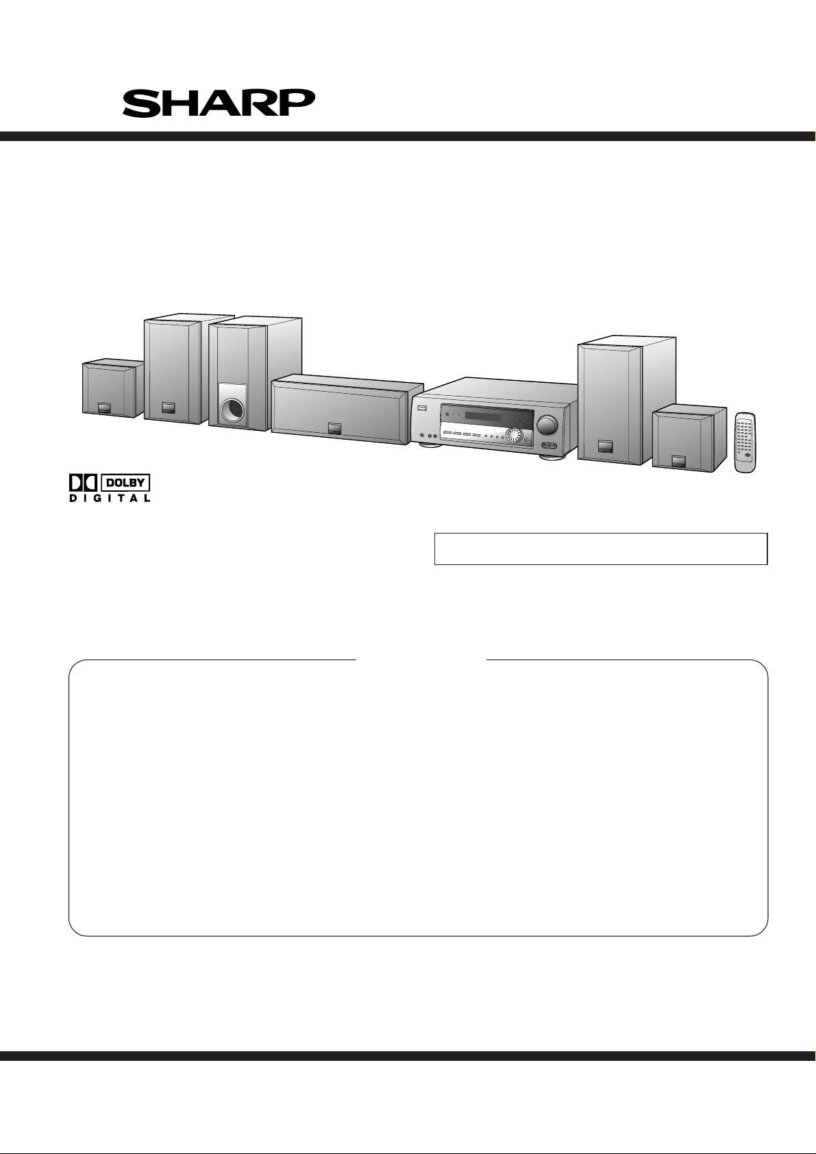
HT-DD5000W
SERVICE MANUAL
No. SX886HTDD500W
HT-DD5000W
HT-DD5000W consisting of HT-DD5000W,CP-F5000W,
CP-SW5000W,CP-C5000W and CP-SR5000W
Manufactured under license from Dolby Laboratories.
"Dolby", "Pro Logic" and the double-D symbol are trademarks of Dolby Laboratories. Confidential Unpublished
Works. 1992-1997 Dolby Laboratories, Inc. All rights re-
served.
• In the interests of user-safety the set should be restored to its original
condition and only parts identical to those specified should be used.
CONTENTS
SPECIFICATIONS .................................................................................................................................................................. 2
VOLTAGE SELECTION......................................................................................................................................................... 2
NAMES OF PARTS ............................................................................................................................................................... 3
OPERATION MANUAL .......................................................................................................................................................... 4
DISASSEMBLY...................................................................................................................................................................... 6
ADJUSTMENT ...................................................................................................................................................................... 8
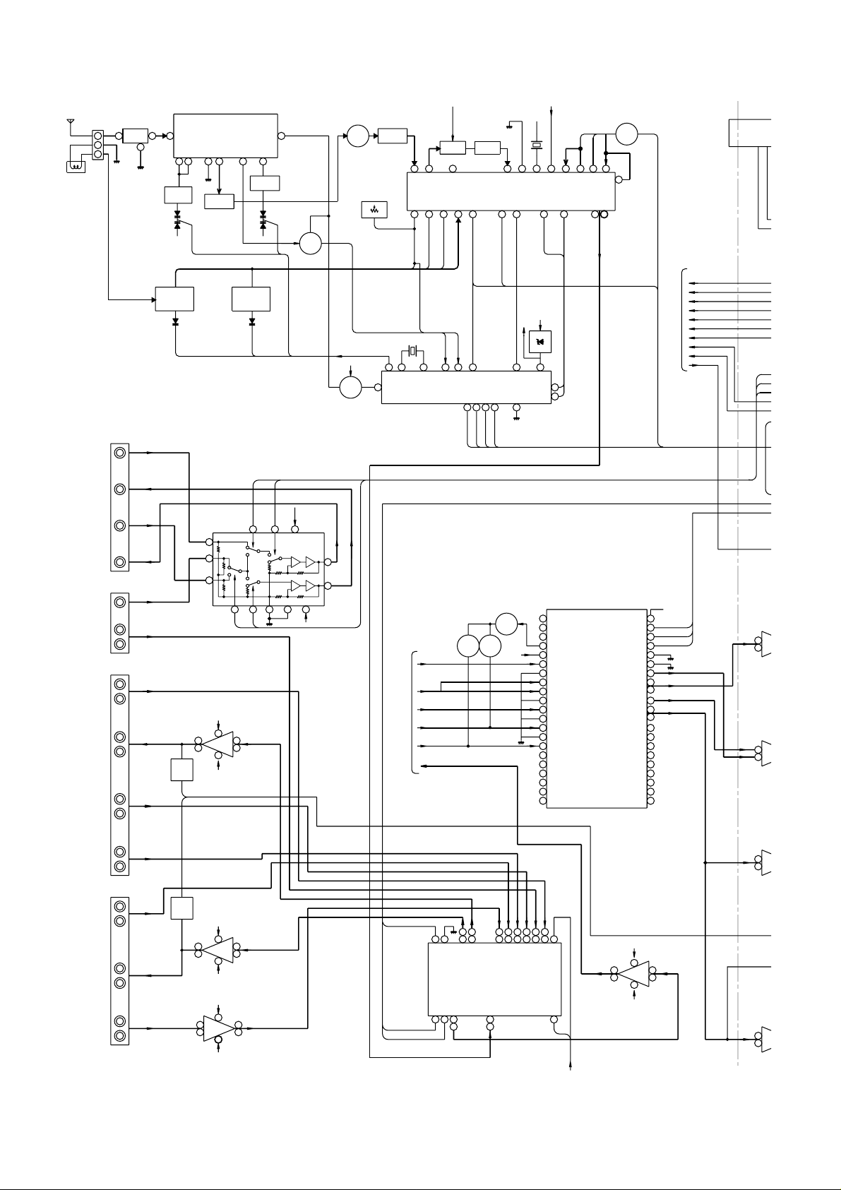
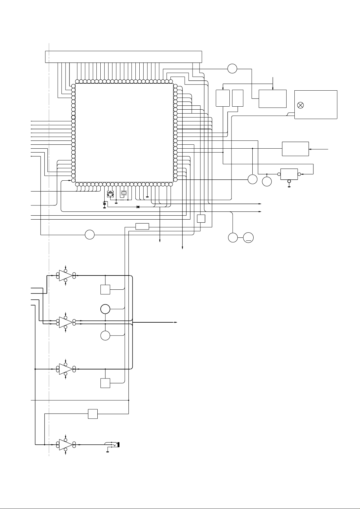
BLOCK DIAGRAM ................................................................................................................................................................ 11
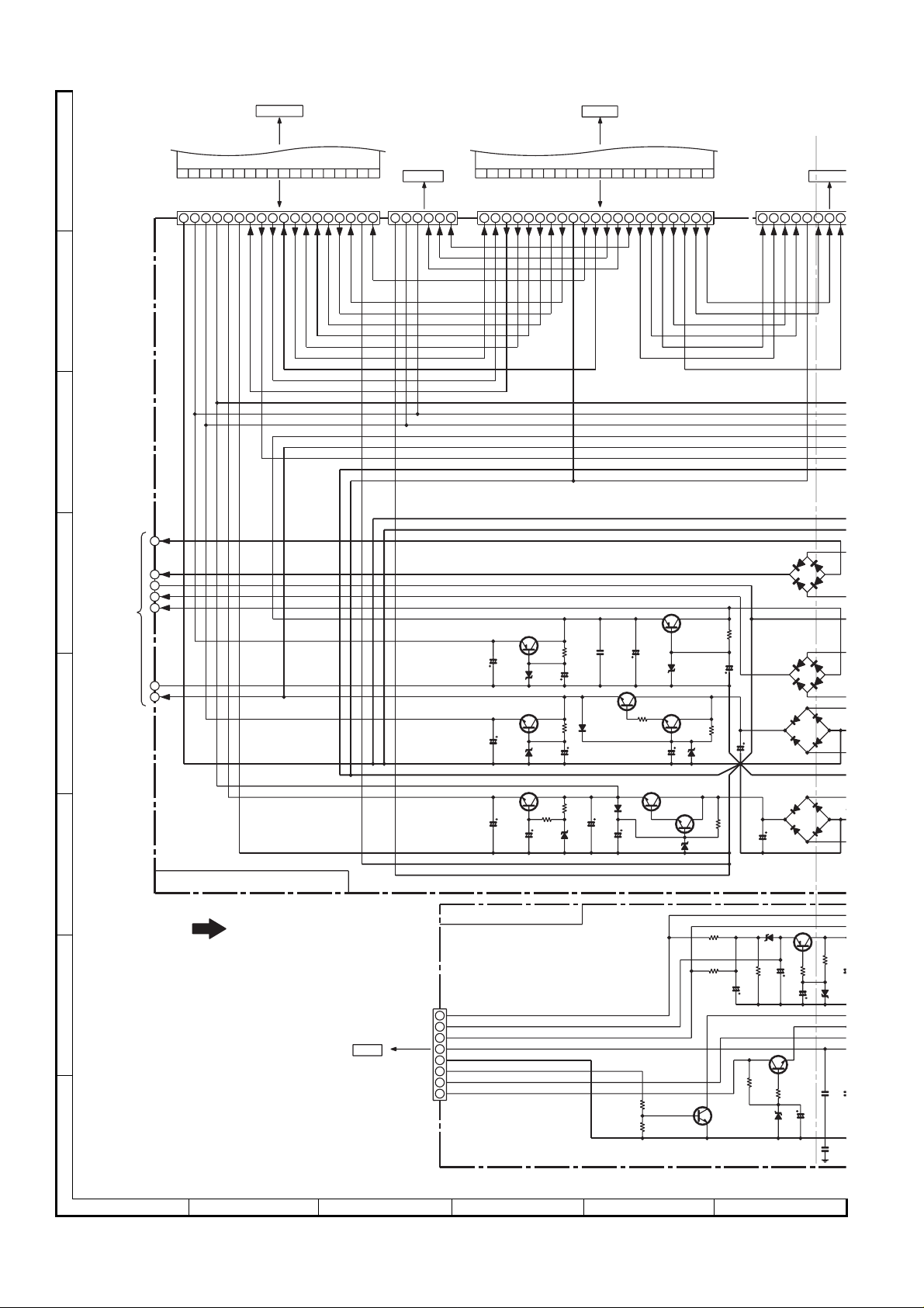
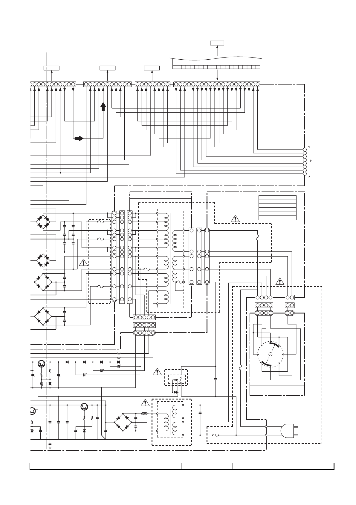
SCHEMATIC DIAGRAM/WIRING SIDE OF P.W.BOARD................................................................................................... 16
NOTES ON SCHEMATIC DIAGRAM .................................................................................................................................. 38
TYPES OF TRANSISTOR AND LED.................................................................................................................................... 38
FUNCTION TABLE OF IC.................................................................................................................................................... 39
FL SEGMENT ...................................................................................................................................................................... 48
PARTS GUIDE/EXPLODED VIEW
Page
SHARP CORPORATION
– 1 –
This document has been published to be used
for after sales service only.
The contents are subject to change without notice.
Page 2
HT-DD5000W
HT-DD5000W
General
Type: Home theater receiver
Power source: AC 110/127/220/230 - 240 V
50/60 Hz
Power consumption: 160 W
Dimenslons: Width; 430 mm (16-15/16")
Height; 150 mm (5-15/16")
Depth; 347 mm (13-11/16")
Weight: 9.8 kg (21.6 lbs.)
Output power: (Front)
RMS; 40 W/CH (0.9% T.H.D.)
(Center)
RMS; 40 W (0.9 % T.H.D.)
(Surround)
RMS; 40 W/CH (0.9 % T.H.D.)
(Sub woofer)
RMS; 40 W (0.9 % T.H.D.)
Output terminals: Front speakers; 8 ohms
Center speaker; 8 ohms
Surround speakers; 8 ohms
Sub woofer; 8 ohms
VCR-1, MD/TAPE, VCR1 VIDEO,
VIDEO MONITOR
Headphones; 16-50 ohms
(recommended; 32 ohms)
Input terminals: DVD (Digital); Coaxial
DVD (Digital); Optical
DVD, VCR-1, VCR-2,CD/AUX,
MD/TAPE; 500 mV/47 kohms
PHONO; 3.5 mV/47 kohms
Tuner section
Frequency range: FM; 88 - 108 MHz
AM; 531 - 1,602 kHz
CP-F5000W
Front speaker section
Type: 2-way, 16 cm (6-5/16") woofer,
and 5 cm (2") tweeter
Maximum Input power: 80 W
Rated Input power: 40 W
Impedance: 8 ohms
Dimensions: Width; 210 mm (8-5/16")
Height; 330 mm (13")
Depth; 218 mm (8-5/8")
Weight: 3.7 kg (8.2 lbs.)/each
SPECIFICATIONS
CP-C5000W
Center speaker section
Type: 2-way, 13 cm (5-1/8") woofer
and 5 cm (2") tweeter
Maximum Input power: 80 W
Rated Input power: 40 W
Impedance: 8 ohms
Dimensions: Width; 400 mm (15-3/4")
Height; 165 mm (6-1/2")
Depth; 163 mm (6-7/16")
Weight: 2.9 kg (6.4 lbs.)
CP-SR5000W
Surround speaker section
Type: 2-way, 13 cm (5-1/8") woofer
and 5 cm (2") tweeter
Maximum Input power: 80 W
Rated Input power: 40 W
Impedance: 8 ohms
Dimensions: Width; 210 mm (8-5/16")
Height; 165 mm (6-1/2")
Depth; 163 mm (6-7/16")
Weight: 1.6 kg (3.5 lbs.)/each
CP-SW5000W
Sub woofer section
Type: 16 cm (6-5/16") super woofer
Maximum Input power: 80 W
Rated Input power: 40 W
Impedance: 8 ohms
Dimensions: Width; 210 mm (8-5/16")
Height; 330 mm (13")
Depth; 340 mm (13-3/8")
Weight: 5.2 kg (11.5 lbs.)
Specifications for this model are subject to change without
prior notice.
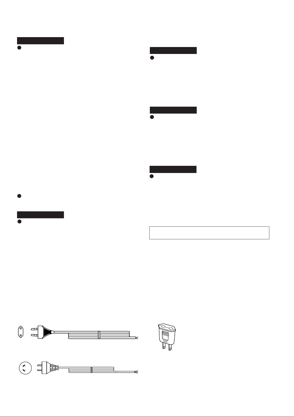
VOLTAGE SELECTION
The voltage selector is located on the AC voltage selector box. If adjustment is necessary, use a screwdriver in order to turn the
selector in either direction until the correct voltage figure is displayed in the window next to the adjustment screw.
QACCE0008AW00
QACCL0005AW00
Figure 2 AC POWER SUPPLY CORD AND AC PLUG ADAPTOR
QPLGA0250AFZZ
– 2 –
Page 3
HT-DD5000W
1
2
7
8
3
4
5
6
9
10
11
12
13
14
HT-DD5000W
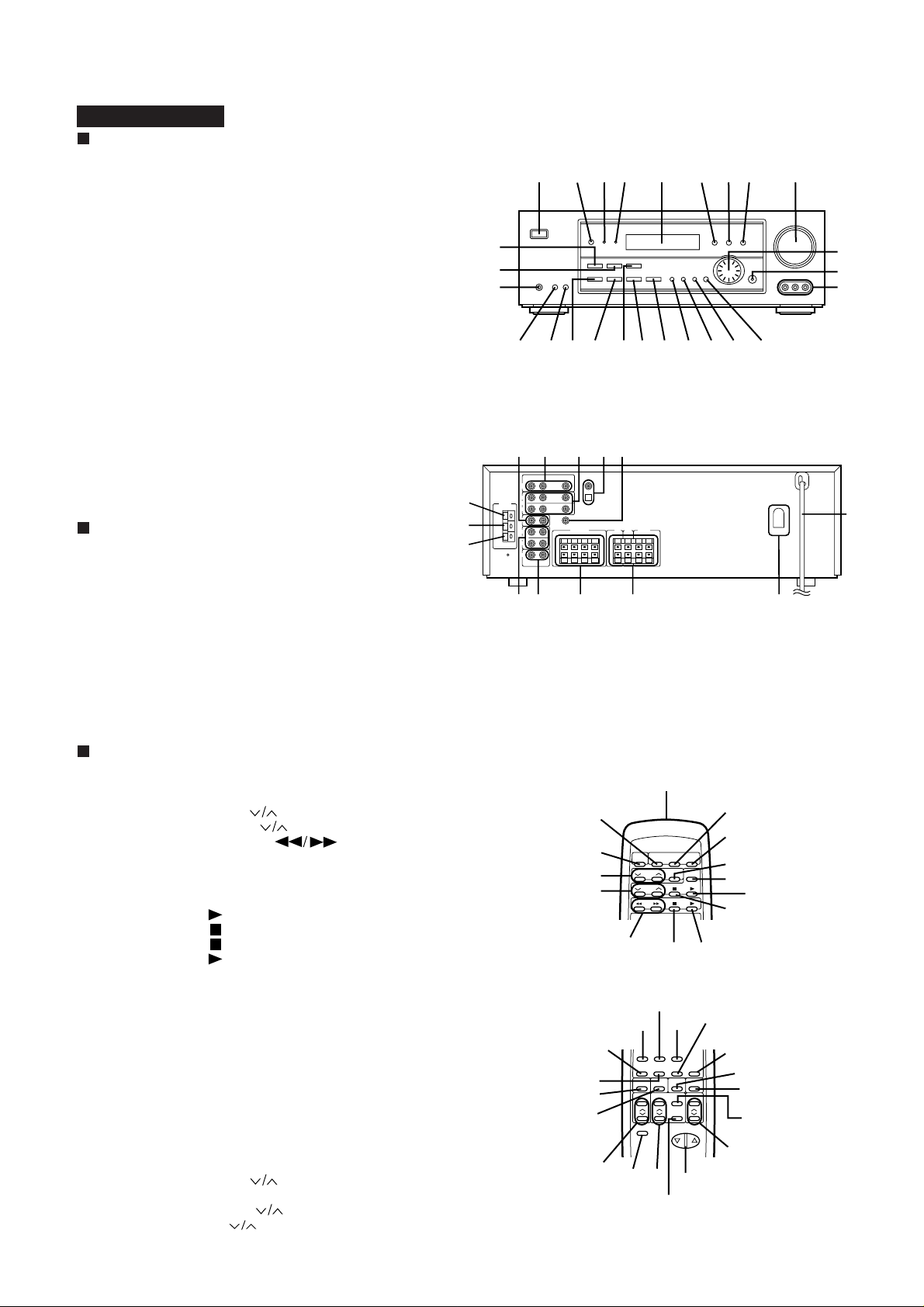
Front Panel
1. On/Stand-by
2. Remote Control Sensor
3. Stand-by Indicator
4. Timer Indicator
5. Display Panel
6. Dolby Surround Button
7. Eqalizer Button
8. Extra Bass Button: X-BASS
9. Volume Conrol
10. DVD Button
11. VCR-1 Button
12. Headphones Socket
13. Speaker A Button
14. Speaker B Button
15. CD/AUX Button
16. MD/TAPE Button
17. VCR-2 Button
18. PHONO Button
19. Tuner (Band) Button
20. Tuning Down Button
21. Tuning Up Button
22. Memory Button
23. Timer/ Sleep Button
24. Jog Dial
25. Enter Button
26. VCR-2 Input Sockets
Rear Panel
27. CD/AUX Input Sockets
28. DVD Input Sockets
29. VCR-1 Input/Output Sockets
30. DVD Digital Input Sockets
31. Video Monitor Output Socket
32. AM Antenna Terminal
33. Antenna Ground Terminal
34. FM Antenna Terminal
35. MD/TAPE Input/Output Sockets
36 Phono Input Sockets
37. Front Speaker Terminals
38. Center/Surround Speaker/Sub Woofer Terminals
39. AC Power Cord
40. AC Voltage Selector
NAMES OF PARTS
1
10
11
12
13 141516 171819 20 21 22 23
2827 29 30 31
32
33
34
35 36 37 38
52 3 94 6 7 8
24
25
26
39
40
Remote Control
1. Remote Control Transmitter LED
2. TV Power Button
3. On/Stand-by Button
4. TV CH Up/Down Button:
5. VCR CH Up/Down Button:
6. DVD Track Up/Down Button:
7. VCR Power Button
8. DVD Power Button
9. TV/VIDEO Button
10. TV/VCR Button
11. VCR Play Button:
12. VCR Stop Button:
13. DVD Stop Button:
14. DVD Play Button:
15. DVD Button
16. VCR-1 Button
17. VCR-2 Button
18. PHONO Button
19. CD/AUX Button
20. MD/TAPE Button
21. Dolby Surround Button
22. Eqalizer Button
23. Tuner (Band) Button
24. Extra Bass Button: X-BASS
25. Preset Balance Button
26. Menu Button
27. Sub Woofer Level Button
28. Mute Button
29. Set Up Up/Down Button:
30. Item Button
31. Volume Up/Down Button:
32. Tuner Preset Button:
– 3 –
19
20
21
22
27
28
15
16
29
30
17
31
18
23
24
25
26
32
Page 4
HT-DD5000W
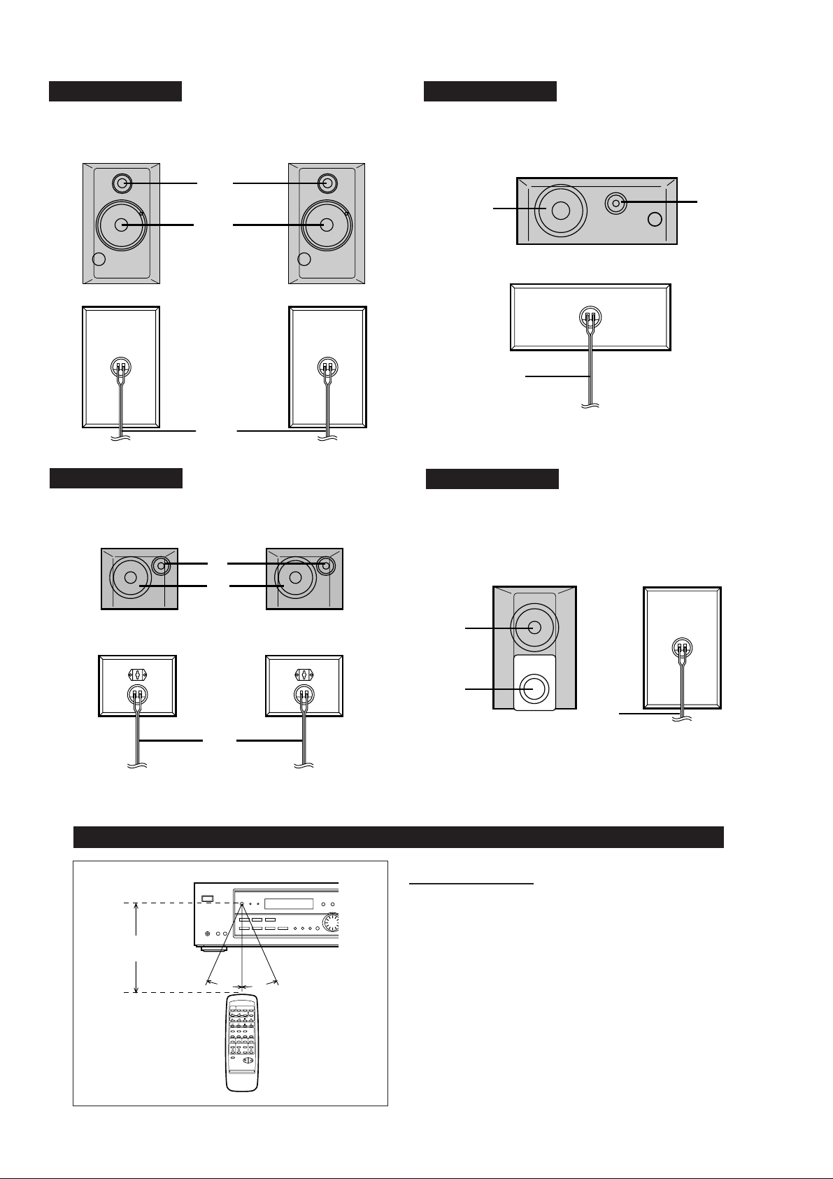
CP-F5000W
1. Tweeter
2. Woofer
3. Speaker Cord
CP-SR5000W
1. Tweeter
2. Woofer
3. Speaker Cord
1
2
3
CP-C5000W
1. Tweeter
2. Woofer
3. Speaker Cord
2
3
CP-SW5000W
1. Woofer
2. Bass Reflex Duct
3. Speaker Cord
1
1
2
3
PREPARATION FOR USE
0.2 m - 6 m
(8" - 20')
15˚
15˚
1
2
OPERATION MANUAL
■
Remote control
● When inserting or removing the batteries, push them towards the battery terminal.
● Installing the batteries incorrectly may cause the unit to
malfunction.
Notes concerning use:
● Replace the batteries if the operating distance is reduced
or if the operation becomes erratic.
● Periodically clean the transmitter LED on the remote con-
trol and the sensor on the main unit with a soft cloth.
● Exposing the sensor on the main unit to strong light may
interfere with operation. Change the lighting or the direction of the unit.
● Keep the remote control away from moisture, excessive
heat, shock, and vibrations.
3
– 4 –
Page 5

HT-DD5000W
CP-F5000W
1. Tweeter
2. Woofer
3. Speaker Cord
CP-SR5000W
1. Tweeter
2. Woofer
3. Speaker Cord
1
2
3
CP-C5000W
1. Tweeter
2. Woofer
3. Speaker Cord
2
3
CP-SW5000W
1. Woofer
2. Bass Reflex Duct
3. Speaker Cord
1
1
2
3
PREPARATION FOR USE
0.2 m - 6 m
(8" - 20')
15˚
15˚
1
2
OPERATION MANUAL
■
Remote control
● When inserting or removing the batteries, push them towards the battery terminal.
● Installing the batteries incorrectly may cause the unit to
malfunction.
Notes concerning use:
● Replace the batteries if the operating distance is reduced
or if the operation becomes erratic.
● Periodically clean the transmitter LED on the remote con-
trol and the sensor on the main unit with a soft cloth.
● Exposing the sensor on the main unit to strong light may
interfere with operation. Change the lighting or the direction of the unit.
● Keep the remote control away from moisture, excessive
heat, shock, and vibrations.
3
– 4 –
Page 6
(Continued)
ON/STAND-BY
HT-DD5000W
■
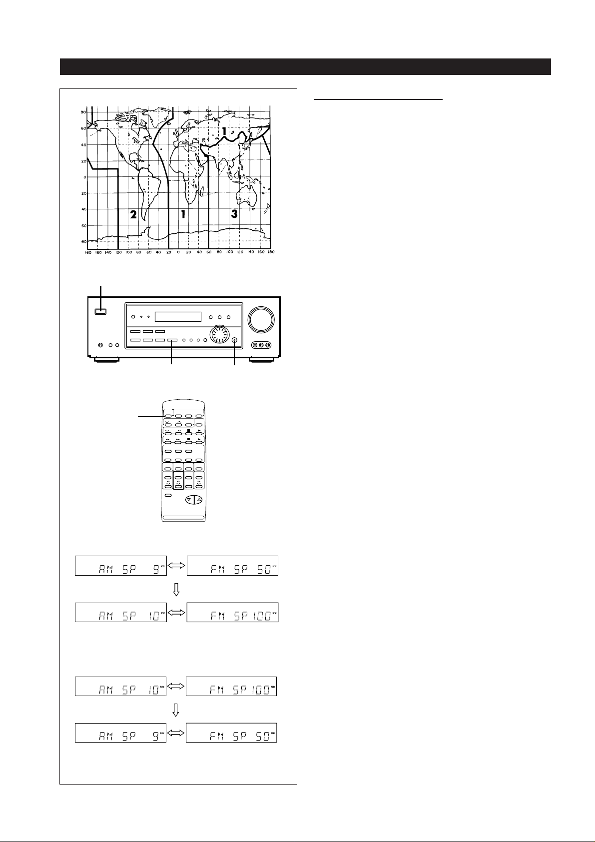
AM/FM Interval (span)
The International Telecommunication Union (ITU) has established that member countries should maintain either a 10
kHz or a 9 kHz interval between broadcasting frequencies
of any AM station. The illustration shows the 9 kHz interval
zones (regions 1 and 3), and the 10 kHz interval zone (region
2).
This product is not equipped with a span selector. However,
it will be adjusted to 9 kHz AM interval (50 kHz FM interval)
when shipped from the factory.
Before using the unit, be sure to set it for the AM tuning
interval (span) used in your area.
To check the tuning span currently selected:
1
Set the ON/STAND-BY button on the main unit to ON.
2
Press the TUNER (BAND) button until "FM" or "AM" appears in the display.
3
Press the TUNER (BAND) button to select the AM band.
● If "AM 531 kHz" is displayed, it means that the radio has
been adjusted for a 9 kHz span. If "AM 530 kHz" is displayed, it means that the radio has been adjusted for a
10 kHz span.
ON/
STAND-BY
[9 kHz → 10 kHz]
[10 kHz → 9 kHz]
TUNER (BAND)
(4 seconds)
ENTER
To change from a 9 kHz AM (50 kHz FM) interval to a
10 kHz AM (100 kHz FM) interval:
1
Press the ON/STAND-BY button on the remote control
to enter the stand-by mode.
2
Hold down the TUNER (BAND) button and the ENTER
button for at least 4 seconds. Release the buttons when
"AM SP 10 kHz" and "FM SP 100 kHz" are displayed
alternately.
To return to a 9 kHz AM (50 kHz FM) interval:
1
Press the ON/STAND-BY button on the remote control
to enter the stand-by mode.
2
Hold down the TUNER (BAND) button and the ENTER
button for at least 4 seconds. Release the buttons when
"AM SP 9 kHz" and "FM SP 50 kHz" are displayed alternately.
Caution:
● When the unit is left for a few hours after the span has
been switched and AC power lead disconnected, it will
be automatically returned to a 9 kHz span. If this happens, set the span again.
● When the span is switched, any stations that are
memorised will be cancelled.
(4 seconds)
– 5 –
Page 7
HT-DD5000W
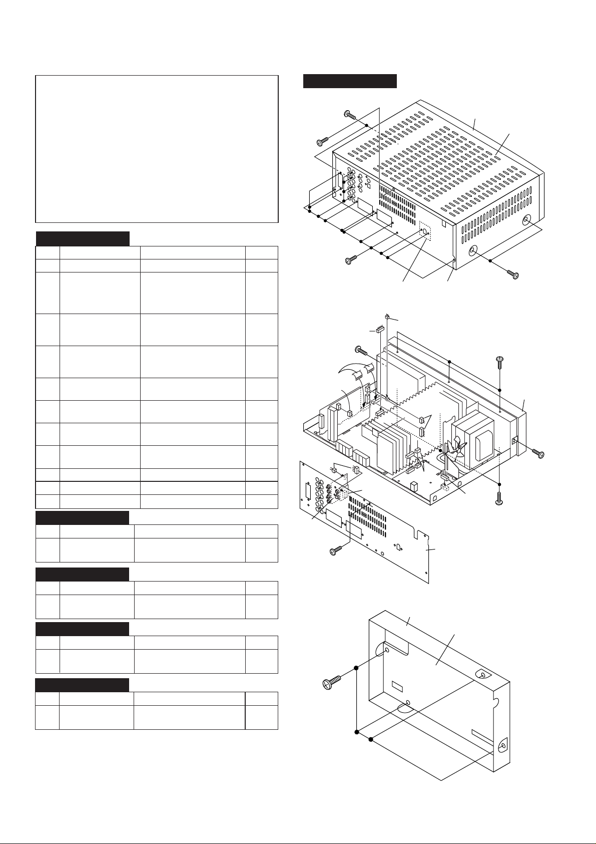
DISASSEMBLY
Caution on Disassembly
Follow the below-mentioned notes when disassembling
the unit and reassembling it, to keep it safe and ensure
excellent performance:
1. Take cassette tape and compact disc out of the unit.
2. Be sure to remove the power supply plug from the wall
outlet before starting to disassemble the unit.
3. Take off nylon bands or wire holders where they need be
removed when disassembling the unit. After servicing
the unit, be sure to rearrange the leads where they were
before disassembling.
4. Take suff cient care on static electricity of integrated
circuits and other circuits when servicing.
HT-DD5000W
REMOVAL PROCEDURESTEP FIGURE
1 Top Cabinet 1. Screw ................. (A1) x5 6-1
2
Rear Panel/Video Jack
PWB/Digital nput Jack
PWB/Voltage Selector
PWB
3
Front Panel
4 Dolby PWB 1. Screw ................. (D1) x3 7-1
5 Main PWB/Tuner 1. Screw ............... (E1) x12 7-1
PWB/Audio PWB 2. Socket ................ (E2) x7
6 Power PWB 1. Screw ................. (F1) x5 7-1
7 Jog Dial 1. Knob ...................(G1) x1 7-2
8 Display PWB 1. Screw ...............(H1) x10 7-2
9 Switch PWB 1. Screw ................. (J1) x2 7-2
10
Headphones PWB
11
VCR Input PWB
CP-F5000W
STEP
1 Woofer/Tweeter 1. Net ........................ (A1) x1 7-3
REMOVAL PROCEDURE
CP-C5000W
STEP REMOVAL PROCEDURE
1 Woofer/Tweeter 1. Net ........................ (A1) x1 7-4
CP-SR5000W
STEP
1 Woofer/Tweeter 1. Net ........................ (A1) x1 7-5
REMOVAL PROCEDURE
1. Screw ............... (B1) x16 6-1,2
2. Socket ............... (B2) x5 6-2
1. Screw ................. (C1) x8 6-2
2. Socket ................ (C2) x5
3. Flat Cable ........... (C3) x2
2. Flat Cable ........... (D2) x2
3. Screw ................. (D3) x4 6-3
2. Socket ................ (F2) x2
2. Nut ......................(G2) x1
2. Socket ................ (H2) x2
1. Screw ................ (K1) x3 7-2
1. Screw ................ (L1) x3 7-2
FIGURE
2. Screw .................... (A2) x6
FIGURE
2. Screw .................... (A2) x6
FIGURE
2. Screw .................... (A2) x6
HT-DD5000W
(A1)x1
ø3x10mm
(B1)x15
ø3x10mm
(C1)x1
ø3x8mm
(C3)x2
(C2)x1
(B2)x2
Video
Jack
PWB
(A1)x2
ø3x10mm
(B2)x1
(B1)x1
ø3x10mm
Voltage
Selector PWB
Digital
Input Jack
PWB
Figure 6-1
(C2)x1
(C2)x2
(B2)x2
Figure 6-2
Shield
Front Panel
Rear
Panel
(C2)x1
Rear
Panel
Dolby PWB
Top Cabinet
(A1)x2
ø3x10mm
(C1)x3
ø3x8mm
Front
Panel
(C1)x1
ø3x8mm
(C1)x3
ø3x8mm
CP-SW5000W
STEP
1 Speaker 1. Net ........................ (A1) x1 7-6
REMOVAL PROCEDURE
2. Screw .................... (A2) x4
FIGURE
(D3)x4
ø3x6mm
Figure 6-3
– 6 –
Page 8
HT-DD5000W
Audio
Jack
PWB
(E1)x2
ø3x8mm
Tuner
PWB
(E2)x2
(E1)x2
ø3x8mm
VCR
Input Jack
PWB
(D1)x1
ø3x8mm
(D2)x1
(E2)x1
(E1)x2
ø3x8mm
(E2)x1
(F1)x1
ø3x8mm
Display
PWB
Power
PWB
Figure 7-1
Front
Panel
(D1)x2
ø3x8mm
(F1)x4
ø3x8mm
(E1)x6
ø3x8mm
(D2)x1
(E2)x2
(G2)x1
(H2)x2
TRANS B
PWB
TRANS A
PWB
(F2)x1
(G1)x1
Switch
PWB
(E2)x1
(F2)x1
CP-C5000W
(A2)x4
Screw
driver
Drive should be pried
away from Speaker Box.
Direction of handle
CP-SR5000W
(A2)x4
(A2)x2
(A1)x1
Figure 7-4
Woofer
Woofer
Tweeter
Speaker
Box
Tweeter
(L1)x3
ø3x10mm
CP-F5000W
(A1)x1
(H1)x10
ø3x10mm
(A2)x2
(J1)x2
ø3x10mm
Figure 7-2
Tweeter
(A2)x4
(K1)x2
ø3x10mm
(K1)x1
ø3x10mm
Woofer
Washer
Speaker
Headphones
PWB
Box
(A1)x1
Screw
driver
Drive should be pried
away from Speaker Box.
Direction of handle
CP-SW5000W
(A2)x4
(A1)x1
(A2)x2
Figure 7-5
Woofer
Speaker
Box
Speaker
Box
Drive should be pried
Screw
driver
away from Speaker Box.
Direction of handle
Figure 7-3
– 7 –
Drive should be pried
Screw
Direction of handle
away from Speaker Box.
driver
Figure 7-6
Page 9
HT-DD5000W
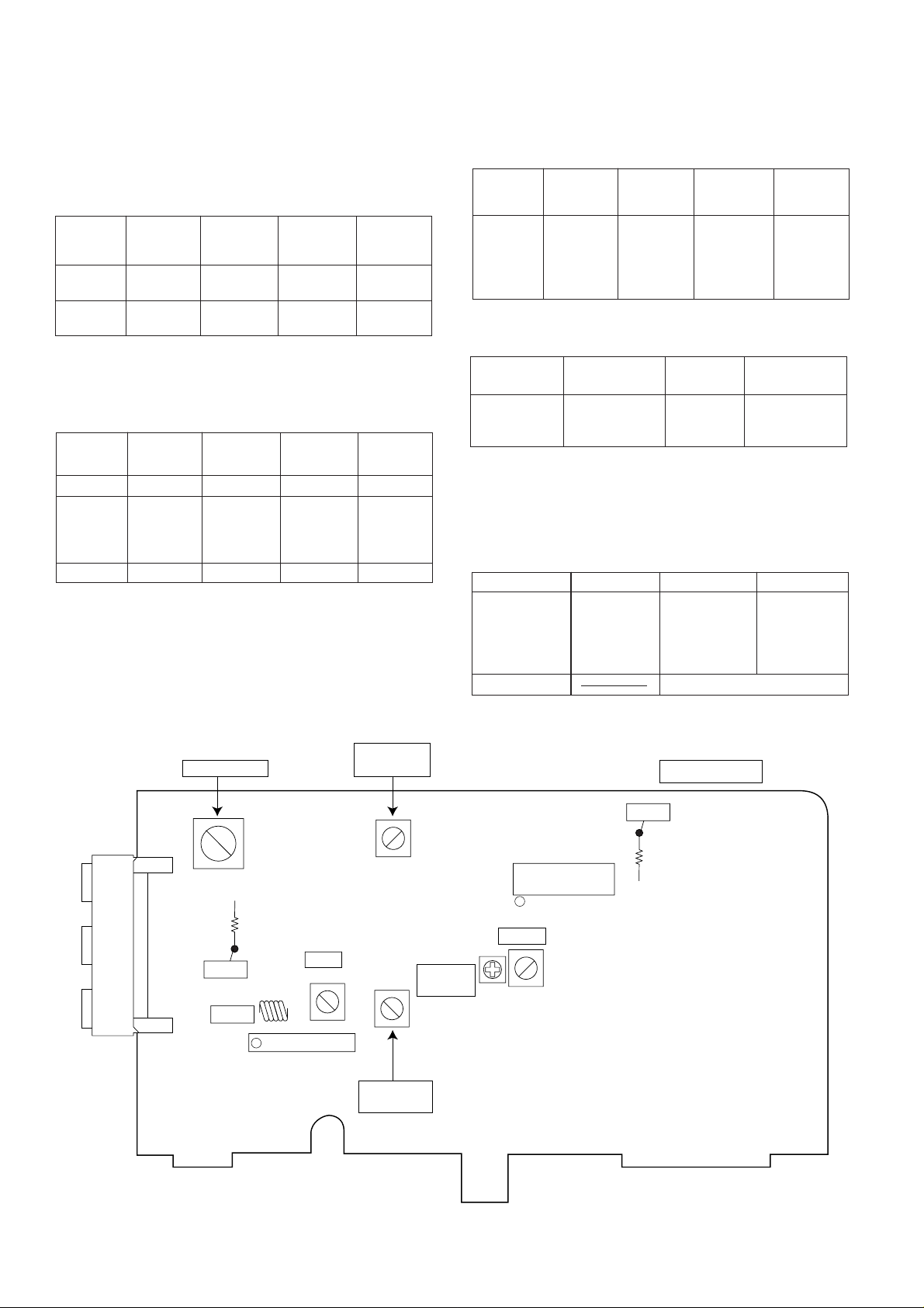
TUNER SECTION
fL: Low-range frequency
fH: High-renge frequency
• FM RF
Signal generator: 1 kHz, 75 kHz dev., FM modulated
Test Stage
Band — 87.5 kHz (fL): L202 *1
Coverage 3.4 ± 0.1 V
RF 98 MHz 98.0 MHz L201 *2
Frequency
(10 - 30 dB)
Frequency
Display
*1. Input: Antenna, Output: TP302
*2. Input: Anetnna, Output: Speaker Terminal
• AM IF/RF
Signal generator: 400 Hz, 30%, AM modulated
Test Stage
IF 450 kHz 1,602 kHz T204 *1
Band — 531 kHz (fL): T203 *2
Tracking 990 kHz 990 kHz T201 *1
Frequency
Frequency
Display
*1. Input: Antenna, Output: TP301
*2. Input: Input is not connected, Output: TP302
Setting/
Adjusting
Parts
Setting/
Adjusting
Parts
(AM Band
Coverage
0.8V±0.1v
Instrument
Connection
Instrument
Connection
ADJUSTMENT
• FM Detection
Signal generator: 10.7 MHz, FM sweep
Test Stage
IF 10.7 MHz 98.0 MHz T202 Input: Pin 1
• FM Mute Level
Signal generator: 1 kHz, 40 kHz dev., FM modulated
Frequency Adjusting
98.0 MHz 98.0 MHz VR201 *1 Input: SOC201
(25 dBµV) Output: Speaker
*1. Adjust so that an output signal appears.
• Setting the Test Mode
Keeping the ENTER button and MEMORY button pressed,
turn on POWER (of Main Set). Then, the frequency is initially
set in the memory as shown in Table. Call it with the JOG to
use it for adjustment and check of tuner circuit.
Preset No.
1 87.50 MHz 6 531 kHz
2 108.00 MHz 7 1,602 kHz
3 98.00 MHz 8 990 kHz
4 90.00 MHz 9 603 kHz
5 106.00 MHz 10 1,404 kHz
11~40
Frequency
Frequency
Display
Frequency
Display
FM Preset No.
Setting/
Adjusting
Parts
(Turn the of IC201
core of T202 Output:
fully counter- Pin 1of
clockwise) IC203
Parts
Instrument
Connection
Instrument
Connection
Terminal
AM
SOC201
ANTENNA
TERMINAL
AM TRACKING
T201
R216
TP302
FM RF
L201
1
IC201
FM IF
T202
AM BAND
COVERAGE
T203
L202
FM BAND
COVERAGE
VR201
FM MUTE
LEVEL
TUNER PWB
TP301
R223
IC 203
1
AM IF
T204
Figure 8 ADJUSTMENT POINTS
– 8 –
Page 10
HT-DD5000W
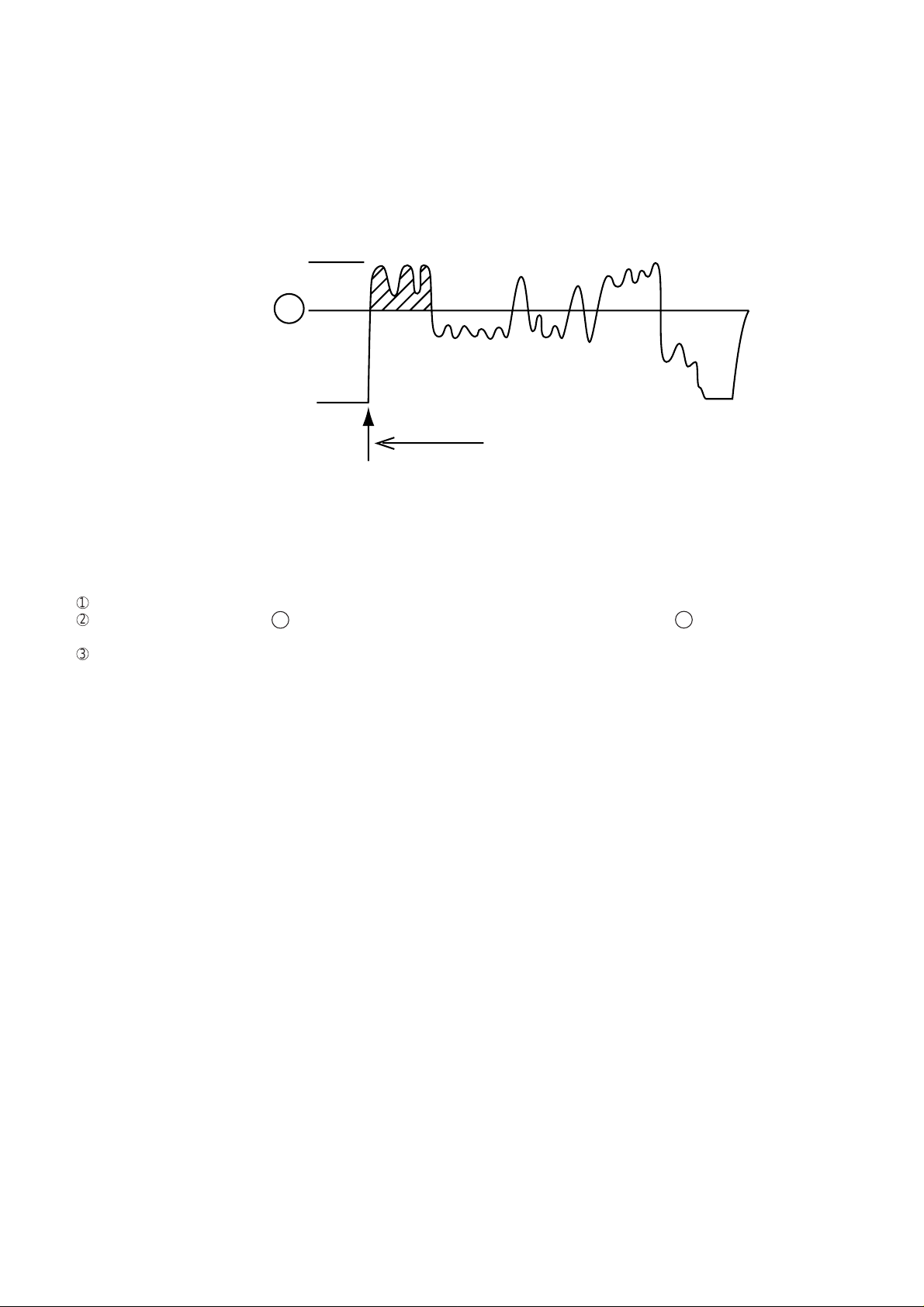
X
0v
(The ALC will be functional
during this period.)
Distortion clip point
SP output
level
Power
ON
EXPLANATION OF AUTOMATIC SOUND VALUE CORRECTION CONTROL
1. Outline
The recent trend is toward rise of SOUND level in the world, for example rock, dancing music, etc. In case of continuous high
level playback and VOL (Volume) are controlled (lowered) automatically after a lapse so as to get the easy-to-listen sound level.
The ALC (Automatic Level Control) of the HT-DD5000 begins to operate immediately after the power is turned on.
2. Explanation of operation
The SOUND operation is explained below.
ALC operation
1
The ALC (Automatic Level Control) will begin operation immediately after the power switch is turned on.
2
If the sound exceeds level X , the ALC will instantaneously cut the volume back to level X , and it will also respond to
monophonic signals.
3
Since this control only effects the VOL level, it does not otherwise change the quality of the sound.
– 9 –
Page 11
HT-DD5000W
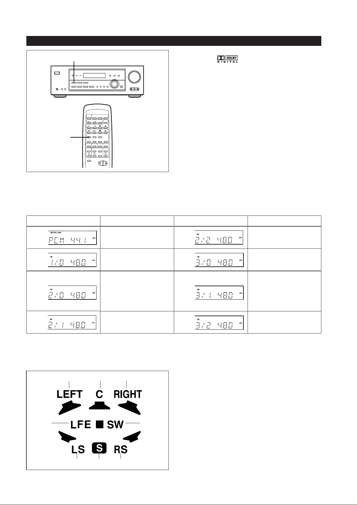
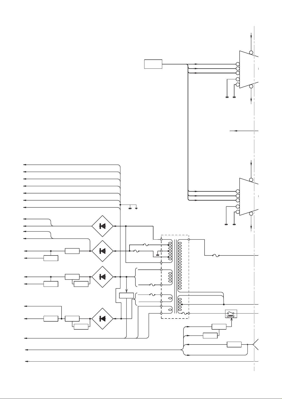
DOLBY DIGITAL
DVD
When you connect this unit to a DVD player which is playing
a disc with the trademark, you can enjoy realistic,
powerful sound by playing back the recorded signal through
6 speakers with the sound coming from the front left, front
right, centre, surround left, surround right and sub woofer
speakers.
To listen to a disc using the Dolby Digital mode:
1 Connect a DVD player.
2 Press the DVD button.
● The current DVD input channel will be displayed. If the
DVD button is pressed whilst the current DVD channel is
DVD
displayed, the input channel (ANALOG, COAXIAL, OPTICAL) can be changed.
3 Start the DVD player.
Note:
● When the Dolby Digital surround mode is being used, the
equalizer will be set to FLAT.
Type of Dolby digital signal
There are different types of Dolby digital signals. When you select COAXIAL or OPTICAL for the DVD input channel, the
following items will be displayed for 2 seconds. They will also be displayed when the DVD player is operating and the DVD
button is pressed.
Display Channels available Display Channels available
Normal PCM playback Front (L, R) + surround
DIGITAL
DIGITAL
DIGITAL
● If a low frequency sound effect (Low Frequency Effect) contains a Dolby digital signal, "LFE" will light in the display.
When this "LFE" is lit, low frequency signals will be output from the sub woofer.
➀
Centre only (monaural) Front (L, R) + centre
Front (L, R)
(When the surround mode
is set to Normal, Phantom
or Wide sound will also be
heard from the surround
speakers.)
Front (L, R) + surround
(monaural)
➁
➂
When Dolby digital signals are input, the display will light up
or go out, as shown to the left.
The channel speaker and SW indicators are used to set the
sound for listening in the surround mode and will light up
according to the speaker signals that are present.
DIGITAL
DIGITAL
DIGITAL
DIGITAL
(L, R)
Front (L, R) + centre +
surround (monaural)
Front (L, R) + centre +
surround (L, R)
➃
➅
➆ ➇
➄
➀ Lights up if the input contains a left channel signal.
➁ Lights up if the input contains a centre channel signal.
➂ Lights up if the input contains a right channel signal.
➃ Lights up if the input contains an "LFE" signal.
➄ Lights up when the amplifier setting will output sound to
sub woofer.
➅ Lights up if the input contains a left surround signal.
➆ Lights up if the input contains surround signals.
➇ Lights up if the input contains a right surround signal.
– 10 –
Page 12

CENTER
SUB
WOOFER
HT-DD5000W
AD RESET
SW-ON
DEMO1
DEMO0
SCK
AC3 RESET
TO DISPLAY SECTION
+7V
6
5
12
Q803
SWITCHING
AC3D_GND
SUB
WOOFER
IN
8
4
13
SUB
WOOFER
AC3_3V
NJM4580M
5
OPE AMP.
4
7
ANALOG SWITCH
8
1
11
2
9
10
OUT
IC811
–7V
IC812
TC4066BF
7
14
A-GND
IC813
NJM4580M
MIX AMP.
–7V
+7V
SUB
WOOFER
+7V
3 5
1
L
FL/FR
MIX
IN
7
R
OUT
–7V
4 8
CENTER
OUT
FL/FR
OUT
SUB
WOOFER
OUT
FR
8
IN
OUT
17
21
11
10
3
1
A_5VA_5V
A-GND
AC3-GND
162022
CONVERTER
6
PD
FL/FR OUT
SCK
RESET
AC3D_GND
SCK_IN
CLK_OUT
CLK_L/R OUT
SL/SR OUT
D-IN
2
1415248 1817
IC810
AK4321VF
D/A
12
7
13
5
XT1
BICK
DEM0
DEM1
CENTER
80
SI
89
87
82
SO
34
SS
3
88
71
68
65
DOLBY AC-3/5.1CH
53
44
GND
37
29
19
8
2
66
95
92
97
91
79
83
21
11
10
3
1
9
LRCK
SUB
CENTER
WOOFER
SUB
WOOFER
ON/OFF
SUB
WOOFER
OUT
54
IC808
ZR38600
MPEG2 AUDIO
DECORDER
61
D-IN
AC3-GND
IN
A-GND
Q801
Q802
99
93
84
81
70
67
59
55
VDD
45
35
30
17
12
6
48
5
90
78
94
86
85
62
60
36
4
FL
2 14
IC809
AK4321VF
D/A
CONVERTER
13
6
5
PD
XT1
DEM0
DEM1
SCK
15
7
BICK
CLK
24
18
9 12
LRCK
FL/FR
CLK_L/R
16 20 22
SI
SO
SS
D_SEL
DEM1
SCK
SL/SR IN
CLK
CLK_L/R
DEM0
16 17 15
PWAD
24
PWDA
23
CONVERTER
5
3 4
AINL+
AINR–
AINR+
OUT
7
6
IC802
NJM4580M
OPE AMP.
A_5V
AINR–
IN
OUT
1
A_5V
4
8 4
A-GND
2
RT_CH
D-OUT
11
12
13
14
IC803
AK4520A
20BIT 2CH
A/D,D/A
202225
2 8
6
19
18
AINL–
AINL+
OUT
7
6
AINL–
IN
NJM4580M
OPE AMP.
1
8
2
ININ
LT_CH
D_SEL
RS OUT
LS OUT
27
26
21
10
A-GND
AC3_3V
9
7
1
IC806
TC74HC15
INVERTER
A_5V
IC805
TC7WU04F
INVERTER
14
6
IN
AC3_3V
D-OUT
9
7
5 3 4
IN
2
16
16
IC801
7
1
6
IN
J802
TOS
GP1F38R
A-GND
DVD
DIGITAL
IN
DVD
DIGITAL
IN
Figure 11 BLOCK DIAGRAM (1/5)
– 11 –
2
15
13
11
8
1
4
3
8
~
AC3D_GND
AC3D_GND
AC3_3V
LS/RS
OUT
Page 13
HT-DD5000W
6
0
0
VH(+)
1
V_GND
AC3D_GND
AC3_GND
D_GND
A_GND
M_GND
P_GND
VH(–)
VH(+)
VL(–)
VL(+)
A-12V(ANALOG)
–7V
A+12V(ANALOG)
+7V
A_5V
AC3_3V
FL VF1,VF2,–VPP
µ-COM
µ-COM_GND
Q406
VOLTAGE
REGURATOR
Q405
VOLTAGE
REGURATOR
Q625
VOLTAGE
REGURATOR
VOLTAGE
REGURATOR
Q620
VOLTAGE
REGURATOR
Q622
Q621
SWITCHING
VOLTAGE
REGURATOR
Q624
Q623
SWITCHING
D621
D622
D623-D626
VOLTAGE
REGULATOR
D627-D630
Q611
VP
T4A L 250V
F607
T4A L 250V
T1A L 250V
T800mA L 250V
VF1
(AC)
VOLUME
SECTION
F606
F611
F608
VF2
(AC)
T602
POWER
TRANSFORMER
T.F
POWER SW
µ-COM5V
230-240V
POW-2
POW-1
L-CH IN
R-CH IN
S_WOOFER IN
REAR_L IN
REAR_R IN
CENTER IN
220V
T2.5A L 250V
127V
110V
Q603
SWITCHING
µ-COM
PROTECT
F601
VOLTAGE
REGULATOR
Q602
REGULATOR
RLY601
SWITCHING
VOLTAGE
Q601
18
22
24
2
3
18
22
24
2
3
IC701
STK41
POWE
8
VH(–)
VH(+)
1
IC751
STK41
POWE
8
VH(–)
D
Figure 12 BLOCK DIAGRAM (2/5)
– 12 –
Page 14
VH(+) VL(+)
HT-DD5000W
1
4
IC701
STK41009
POWER AMP.
7
8
VH(–) VL(–)
VH(+) VL(+)
1
4
IC751
STK41009
POWER AMP.
7
8
µ-COM
POSISTOR
12
Q703
Q704
Q705
Q753
Q754
Q755
µ-COM
POSISTOR
12
µ-COM
SO651
A-SP
B-SP
14
15
26
Q706
Q707
Q756
Q757
26
15
14
SWITCHING
SW RLY
C-RLY
RLY651
Q651
Q654
RLY652
Q652
Q655
RLY653
Q653
RLY654
Q656
RLY681
Q682
RLY682
SWITCHING
SWITCHING
SWITCHING
SWITCHING
FRONT-A L-CH OUT
FRONT-A R-CH OUT
FRONT-B L-CH OUT
SP-A
SP-B
SUPER WOOFER OUT
CENTER OUT
REAR L-CH OUT
FRONT
SPEAKER
TERMINAL
FRONT-A
+
L-CH
GND
–
GND
–
FRONT-A
+
R-CH
FRONT-B
+
L-CH
GND
–
GND
–
FRONT-B
+
R-CH
SP-A/B
SELECT
SWITCH
CENTER/SURROUND
/SUB WOOFER
SUPER
+
WOOFER
GND
–
GND
–
CENTER
+
SURROUND L-CH
+
SO681
SPEAKER
TERMINAL
VH(–) VL(–)
HING
D601-D604
POWER
TRANSFORMER
T601
VOLTAGE
SELECTOR
F603
T100mA L 250V
R-RLY
F602
T5A L 250V
AC POWER SUPPLY CORD
AC 110/127/220/230-240V
50/60Hz
Q681
SWITCHING
SWITCHING
REAR R-CH OUT
GND
–
GND
–
SURROUND R-CH
+
Figure 13 BLOCK DIAGRAM (3/5)
– 13 –
Page 15
HT-DD5000W
F
C
M
F
C
M
D
A
C
M
E
4
4
E
E
SOC201
FM ANT
ANTENNA
TERMINAL
AM LOOP ANT
VCR1
VIDEO
INPUT
VCR1
VIDEO
OUTPUT
VIDEO
INPUT
MONITOR
OUTPUT
VCR2
VIDEO
INPUT
VCR2
AUDIO
INPUT
VCR1
INPUT
VCR1
OUTPUT
INPUT
CD/AUX
INPUT
MD/TAPE
INPUT
MD/TAPE
OUTPUT
PHONO
INPUT
DVD
DVD
BAND PASS
FILTER
BF201
1 3
J401
J404
J405
L
R
L
R
L
R
J406
L
R
L
R
L
R
+B12V
IF AMP
1
3
FM RF
L201
AM ANT
T201
OUT
Q505
Q506
Q507
Q508
4
AM RF
SWITCHING
MUTE
SWITCHING
OUT
IN
TA7358AP
6
5
FM IF
T202
VIDEO SWITCH
IC403
NJM2279D
12
3
1
2
V_SW1
BUFFER AMP.
IC411
NJM4565M
+7V
8
1
3
5
7
4
–7V
BUFFER AMP.
IC412
NJM4565M
+7V
8
1
3
7
5
4
–7V
MOTOR DRIVE
IC404
NJM4558M
+7V
8
1
3
7
5
4
–7V
2
L
R
L
R
MUTE
7
OSC
T203
MUT2
IN
8
FM IF
VT
FM OSC
L202
AM OSC
V_SW2
4
IN
OUT
7
MUT1
1113
9
FM IF
AMP
6
FMOSC
Q201
FM +B
+7V
8
10
Vout1
5
Vout2
14
–7V
IC201
FM FRONT END
FM IF
CF201 Q281
FM IF IN
VR201
FM MUTE LEVEL
X352
4.5MHz
VT
A+12V
20
FM
Q203
7
AM IF
T204
CF203
2
1
3
OUT
REQ
IC203
LA1833
FM/AM IF MPX.
AM
OSC
21222324
7
IN
AFC
OUT
22 15 16 11 12 17
1
OSC
FRONT LEVEL
ADJUSTING
SUB-W
LS/RS
CENTER
FR
DOLBY SECTION
FL
LT/RT_CH
STEREO
AM RF IN
STEREO
XT21
FM IN
AM IN
IC202
LC72131
PLL (TUNER)
3
4
DICLCE
18
19
10
1314
11
S9
CK
S10
GND
TC9273F
FUNCTION SWITCH
S11
STB
DATA
151617
12
5
Q504Q503
IC402
21
8
S7
AM IF
6
SD
6
DO
Q501
22
S6
+B12V
FM IF
CF202
17
8
4
9
5
FM
GND VCC
DET
IF
OUT
PHASE
AM/FM
MPX
VCO
CUT
VOLTAGE
REGURATER
A+12V
+B5V
+5V
IF IN
10
9
21
M62446FP
6CH ELECTRONIC VOLUME
OUT4(NC)
1
2
OUT3(NC)
3
OUT2(NC)
4
OUT1(NC)
5
+7V
AVDD
SWIN
6
GNDS
7
SRIN
8
SLIN
9
GNDC
10
11
C_IN
12
GNDR
13
R_IN
14
GND
15
L_IN
16
BYPASSR(NC)
17
BYPASSL(NC)
18
LTRE(NC)
19
LBYPASS3(NC)
20
LBYPASS2(NC)
21
LBYPASS1(NC)
2726252423
1
4
5 6 7
2
3
S1S2S3S4S5
VSS
VDD
28
A+12V
18 19 16
AM
FM
OUT
L
IC401
OUT
A–12V
MUTING
Q202
15
OUT
MPX
IN
1413121110
R
DVDD
DATA
LATCH
D_GND
A_GND
SW_OUT
RR_OUT
RL_OUT
C_OUT
R_OUT
L_OUT
AVSS
CL1(NC)
CL2(NC)
CR1(NC)
CR2(NC)
RTRE(NC)
RBYPASS3(NC)
RBYPASS2(NC)
RBYPASS1(NC)
+7V
1
7
–7V
OPE AMP.
IC405
NJM4580M
TUNER MUTE
SD
42
41
CLK
40
39
38
37
36
35
34
33
32
31
30
29
28
27
26
25
24
23
22
8
3
5
4
AD RESET
AC3-RES
AC3-SS
AC3-SI
D-SEL
AC3-SCK
SW-ON
DEM0
DEM1
TO DOLBY SECTION
AC3-SO
+B5V
IN
D
D
BUFF
IC
NJM
3
5
IN
BUF
I
NJ
3
5
IN
BUF
I
NJ
3
5
IN
HEA
I
NJ
3
5
IN
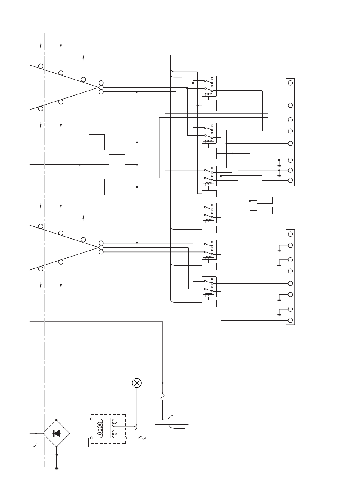
Figure 14 BLOCK DIAGRAM (4/5)
– 14 –
TO POWER SECTION
Page 16
HT-DD5000W
AD RESET
AC3-RES
AC3-SS
AC3-SI
D-SEL
AC3-SCK
SW-ON
DEM0
DEM1
AC3-SO
P14
DEM0
DEM1
VPP
BUFFER AMP.
IC408
NJM4565M
A+12V
8
3
5
IN
4
A–12V
BUFFER AMP.
IC407
NJM4565M
A+12V
8
3
5
IN
4
A–12V
BUFFER AMP.
IC406
NJM4565M
A+12V
8
3
5
IN
4
A–12V
P13
76
77
78
79
81
82
83
84
85
86
87
88
89
90
91
92
93
94
95
96
97
98
99
100
80
1
7
1
7
1
7
737475
P9P8P7P6P5P4P3P2P1
P12
P11
P10
P15
P16
NC
NC
NC
NC
DAPD
ADPD
AC3–RES
AC3–SS
AC3–SI
D–SEL
AC3–SCK
SW–ON
PRO–ENA
PRO–DI
PRO–CK
V–SW1
V–SW2
V–MUTE
TUN–DI
TUN–DO
TUN–CK
TUN–CE
1 2 3 4
SWITCHING
Q9
OUT
R_MUT
C_MUT
OUT
SW_MUTE
OUT
F_MUT
707172
IX0004SJ
SYSTEM
MICROCOMPUTER
TUN–MUTE
TUN–SD
TUN–ST
VDD
OSC2
OSC1
VSS XIXO
10 11 12 13 14 15 16
9
8
6
5
7
XL2
8 MHz
REAR2 L,R
Q411
Q412
SWITCHING
SWITCHING
Q409
CENTER
S_WOOFER
Q410
SWITCHING
FRONT L,R
Q407
Q408
SWITCHING
FL1
DISPLAY
5960616263646566676869
9G8G7G6G5G4G3G2G1G
10G
IC1
MMOD
VREF–
KEY1
17
XL1
32.768 kHz
BACK UP
SWITCHING
Q1~Q4
TO POWER AMP. SECTION
58
KEY2
KEY3
AREA
SP–LEVEL
MODEL
18 19 20 23
21 22
µ–COM25V
FAN
PROTECT
LED1
53
54555657
5152
50
SPSWB
49
SPSWA
48
SW–RLAY
47
C–RLAY
46
R–RLAY
45
HP MUTE
44
POW–SW
FA–RLAY
43
SW–MUTE
42
C–MUTE
41
R–MUTE
40
F–MUTE
39
JOG DOWN
38
JOG UP
37
REMOCON
36
AC3–SO
35
SYS–STOP
34
POWER
33
V–DATA
32
V–CK
31
V–LACH
30
FS–CK
29
FS–DATA
28
FS–STB
27
RESET
26
POSISTER
24 25
ALC
VREF+
TO POWER AMP. SECTION
SPEAKER A,B SW
VF1
(AC)
VF2
(AC)
Q11
Q12
SWITCHING
POWER
SW1
Q10
JOG
SW23
Q6
RESET
TO POWER AMP SECTION
TO POWER SECTION
Q671
M
Q672
µ–COM25V
STAND–BY LED
LED1
TIMER LED
LED2
REMOCON
Q13
M671
FAN
MOTOR
1
RX1
REMOTE
SENSOR
2
Q7
Q8
ZD1
3
KEY MATRIX
SW4–SW8
SW9–SW15
SW16–SW19
µ–COM25V
HEADPHONE
AMP.
IC581
NJM4565D
8
3
5
IN
4
A+12V
A–12V
SWITCHING
HP_MUTE
Q413
Q414
OUT
1
7
J581
HEADPHONES
Figure 15 BLOCK DIAGRAM (5/5)
– 15 –
Page 17
HT-DD5000W
6
0
C626
3
4
7
4
P
A+12V
A
FC801
TO DOLBY PWB
P24 5-H
CNS801A
TO VIDEO
JACK PWB
P20 5-A
CNS403
FC1
21
18
1
TO DISPLAY PWB
P22 1-E
CNS1A
TO TUNER
1
P27 12-G
CNS201
B
C
D
E
F
TO POWER
AMP.SECTION
P18 1-E
18 17 16 15 14 13 12 11 10
–7V
+7V
A_5V
AC3_3V
AC3_SO
AC3_GND
+B
–B
+B
7
6
5
4
3
–B
2
A+12V
1
+B
+B
+B
–B
MAIN PWB-A(1/2)
987654321
–B
+B
+B
AC3D_GND
6
+B
4 3 2 1
5
–B
V_MUTE
V_SW1
V_SW2
AC3_SCK
AC3_SI
AC3_SS
AC3_RES
ADPD
DAPD
D_SEL
SW_ON
DEM0
DEM1
VH(–)
VH(+)
P_GND
VL(+)
VL(–)
A–12V
–7V
M_GND
A+12V
+7V
A_GND
D_GND
A_5V
AC3_3V
AC3_GND
AC3D_GND
V_GND
VOLTAGE
REGURATOR
C475B
10/50
CNS1B CNP403CNS801B
20
18
21
19
17
TO AC3
Q406
2SB562 C
VOLTAGE REGURATOR
–7.2V
–B
C476B
10/50
ZD402
MTZJ7.5C
Q405
2SD468 C
7V 12.2V
ZD401
MTZJ7.5C
VOLTAGE
REGURATOR
3.4V
4.0V
C641
1000/6.3
C640
47/25
16
15
–12V
–7.8V
R495B
270
7.6V
Q625
2SD468 C
4.9V
R628
22
14
+B
ZD624
MTZJ3.9B
13
11
12
R496B
270
C478
1/50
12.2V 16.9V
VOLTAGE
REGURATOR
D631
1N4148
C477
1/50
R627
82
10
C639
C628
+B
220/16
8
9
7
0.022
2SD2012 Y
13V
R624
47
Q621
KTC3199 GR
Q624
2SD2012 Y
4.9V
D632
1N4148
C638
47/25
4 3 2 1
6
5
–12V –21.6V
–12.8V
REGURATOR
C627
220/25
Q622
13.6V
C634
47/25
VOLTAGE
REGURATOR
11.6V
Q623
KTC3199 GR
5.5V
SWITCH
ZD623
MTZJ6.2B
Q620
2SB1375 Y
VOLTAGE
ZD621
MTZJ13A
SWITCH
16.9V
R622
1K
ZD622
MTZJ130C
R625
6.18V
CNP201
8
9
+
+
D626
D630
D_GND
~
~
~
~
7
6
–
–
D62
1N400
1N400
5
C
D62
11
10
12
TUN_ST
TUN_SD
TUN_CE
TUN_DI
TUN_CK
TUN_DO
TUN_MUTE
D621
BR102J02
1.5K
R620
D622
BR102J02
C629
47/25
+B
D624
1N4004S
D625
C633
4700/25
1N4004S
1N4004S
+B
D628
C637
3300/25
1N4004S
D629
1N4004S
1N4004S
11.6V
330
FM SIGNAL
G
TO DISPLAY PWB
P23 7-H
CNS4
H
NOTES ON SCHEMATIC DIAGRAM can be found on page 38.
1
23456
Figure 16 SCHEMATIC DIAGRAM (1/12)
POWER PWB-D2
VF1
1
–VPP
2
VF2
3
µ–COM_5V
4
D_GND
5
POW_SW
6
POW_1
7
POW_2
8
CNP4
– 16 –
R607
10K
R608
47K
0.5V
SWITCHING
Q603
KTC3199 GR
R617
220
R616
220
0V
0V
ZD612
MTZJ6.8C
R615
C617
100/35
VOLTAGE
REGULATOR
Q602
2SD468 C
ZD602
MTZJ5.6B
12K
7.3V
R606
1K
–32V –35.9V
–32.6V
100
R614
C616
100/35
C615
47/50
4.7V
5.3V
R605
47
C619
0.047
VOLTAGE
Q611
KTA1266 GR
C618
C606
47/16
2.2K
R613
ZD611
MTZJ330C
0.047
Page 18
100/35
TO DISPLAY PWB
5
3V
P23 12-D
CNS2A
HT-DD5000W
201
1
10
1
J02
+
22
2J02
+
24
04S
5
4S
D626
1N4004S
628
4004S
629
004S
D630
1N4004S
TO TUNER PWB
P27 12-G
CNS201
8
9
6
7
D_GND
~
–
~
~
–
~
D623
1N4004S
D627
1N4004S
4 3 2 1
5
A+12V
TUN_R
+B
C623
C624
0.1
C626
0.047
A_GND
0.1
C625
0.047
C631
0.047
C632
0.047
C635
0.047
C636
0.047
TUN_L
C621
0.1
C622
0.1
CNP502
A_GND
4 3 2 1
A–12V
A+12V
TUN_R
–B
+B
F606
T4A L 250V
F607
T4A L 250V
F608
T800mA
L 250V
TO AUDIO
JACK PWB
P21 10-A
CNS502
6
5
TUN_L
D_GND
7
FS_CK
13
12
11
10
9
8
7
6
5
4
3
2
1
BI602
TO AUDIO
JACK PWB
P21 9-A
CNS501
CNP501
10
8
9
FS_STB
FS_DATA
–7V
–B
11
+7V
+B
V_CK
V_DATA
V_LATCH
4 3 2 1
A_5V
+B
TRANS A/B PWB-D3,D4
13
13
12
12
11
11
10
10
9
9
8
8
7
7
6
6
5
5
F611
T1A L 250V
4
4
3
3
2
2
1
1
CNS602
CNP602
4 3 2 1
5
4 3 2 1
5
4 3 2 1
5
1
CNS2B
8
6
5
7
F_MUTE
R_MUTE
C_MUTE
FAN_SW
SW_MUTE
POWER TRANSFORMER
CNP603
CNS603
BI603
PROTECT
T602
T.F.
AC3_SO
C_RLY
SW_RLY
CNP601
1
2
3
4
5
R_RLY
CNS601
1
2
3
4
5
9 8 7 6 5 4 3 2 1
FA_RLY
SW_MUTE
BI601
1
2
3
4
5
C_MUTE
R_MUTE
220/230-240V
127V
110V
0V
V_DATA
F_MUTE
V_CK
16 15 14 13 12 11 10
FS_CK
V_LATCH
18 17 20 19
FS_STB
FS_DATA
F601
FC2
20
SP_LEVEL
POSISTOR
SWITCH POSITION
VOLTAGE
110V
127V
220V
230-240V
T2.5A L 250V
No.
3-4, 7-8
8-1, 4-5
2-3, 6-7
1-2, 5-6
CNP6A4
1 1 2 2 3 4
1 1 2 2 3 4
CNS6A4 CNS6B4
1 1 2 2 3 4
CNP6B4
BI6B4 BI6A4
8
9
10
11
12
13
14
15
TO POWER
AMP.SECTION
P18 1-E
P18 1-B
VOLTAGE REGULATOR
–32V –35.9V
–32.6V
100
R614
C615
47/50
4.7V
.
R605
47
C606
C619
0.047
R613
Q611
KTA1266 GR
ZD611
C618
0.047
47/16
7
1N4004S
2.2K
C614
220/63
MTZJ330C
C607
0.022
D614
D613
1N4004S
C613
47/63
Q601
2SD468 C
VOLTAGE REGULATOR
C605
0.022
C604
5.6V
47/16
R604
47
7.2V
6.3V
820
R603
ZD601
MTZJ6.8A
C609
7
6
5
4
3
AC110/127/220/230–240V
8
1
2
AC POWER
SUPPLY CORD
50/60Hz(220)
D612
1N4004S
C612
100/50
0.047
R611 1
R612 1
+B
D602
1N4004S
D603
1N4004S
C603
2200/16
C611
100/50
D611
1N4004S
D601
1N4004S
D604
1N4004S
R610
THERMISTOR
C601
0.047
C602
0.047
SWITCHING
RLY601
D607
1N4004
T601
SUB POWER TRANSFORMER
C608
0.0047
C610
0.0047
T100mA L 250V
F603
SW601
VOLTAGE
SELECTOR
F602
T5A L 250V
VOLTAGE SELECTOR
PWB-D9
(242)
(242)
8 9 10 11 12
Figure 17 SCHEMATIC DIAGRAM (2/12)
– 17 –
Page 19
HT-DD5000W
D677
6
N
D674
Q707
R
A
B
C
D
E
F
P21 12 - D
TO AUDIO JACK PWB
G
P17 12 - C
TO MAIN SECTION
CNS701
P21 12 - E
TO AUDIO JACK PWB
TO MAIN SECTION
P16 1 - D,P17 12 - C
1
2
3
CNP702
4
5
CNS702
MAIN PWB-A (2/2)
38V
9
CNP701
FRONT_L
5
4
3
2
1
5
14
4
3
10
13
1
2
6
7
15
8
12
11
1
2
3
4
5
BI702
POSISTOR
A_GND
FRONT_R
SW
P_GND
PROTECT
+VL
–VL
FA_RLY
SW_RLY
A+1_V
M_GND
+VH
–VH
FAN_SW
SP_LEVEL
C_RLY
R_RLY
CENTER
REAR_R
A_GND
REAR_L
1
C733
100/50
C783 100/50
1 2 3
23V
0V
2 3
ZD701
D741
1N4004
C751
4700/ 50
D781
24V
4
5
D705
1N4148
MTZJ7.5C
3.9K
R744
C731
D731
1N5402M
C701
4700/35
1N5402M
C781 100/35
R794
3.9K(1/4W)
ZD751
MTZJ7.5C
D755
1N4148
5
4
–18V
19V
6
D706
1N4148
R745
100/35
C732 100/35
C702
4700/35
C752
4700/50
C782 100/35
R795
3.9K(1/4W)
D756
1N4148
6
–24V
–39V
–23V
–23V
–23V
11
10
8
7
9
R742 100(1/2W)
R743
ZD702
MTZJ7.5C
100(1/2W)
3.9K
Q703
KTC3199 GR
C735
100/50
D732
C734
100/50
1N5402M
D782
1N5402M
C784 100/50
C785 100/50
C786 100/50
Q753
ZD752
MTZJ7.5C
R793
100(1/2W) Fusible
R792 100(1/2W) Fusible
10
11
7
8
9
STK41009
POWER AMP.
FM SIGNAL
IC701
STK41009
POWER AMP.
0V
0V
12 13
C725
0.022(ML)
R731
4.7K
0V
0V
R729
4.7K
5V
D701
1N4148
C713
R716
15P
1K
R718
56K
L701
0.3µH
R701
4.7(1/2W)
C721
0.22(ML)
C719
0.22
C736
100/50
(ML)
D740
1N4004
C771
0.22(ML)
R771
C769
4.7(1/2W)
0.22
L751
0.3µH
(ML)
0.3µH
R751
4.7(1/2W)
R768
56K
R766
C763
1K
15P
D751
1N4148
R779
4.7K
KTC3199 GR
R781
4.7K
C775
0.022(ML)
12
13
IC751
–37V
14
15
16
0V
0V
R725
R728
0.2(1W)
R727
R726
0.2(1W)
0.2(1W)
R715
1K
L702
C720
0.22
(ML)
R721
4.7(1/2W)
C770
0.22
L752
(ML)
R765
1K
R776 0.2(1W)
R775 0.2(1W)
R777 0.2(1W)
14
15
16
17
37V
KTC3199 GR
0.2
(1W)
4.7K
C726
R730
0.022
1N4148
C714
15P
R717 56K
R702
4.7
(1/2W)
0.3µH
C705
2.2/50
C722
0.22(ML)
C772
0.22(ML)
R752
4.7(1/2W)
C755
2.2/50
C754
2.2/50
R767
56K
C764
15P
1N4148
R778
0.2(1W)
R780
4.7K
C776
0.022
(ML)
17
Q704
R732
4.7K
(ML)
D702
C704
2.2/50
D752
R782
4.7K
+
–
0V
C703
2.2/50
R707
56K
R722
4.7
(1/2W)
R772
4.7(1/2W)
R757
56K
C753
2.2/50
C757
47P
–
+
18
19
0V
0V
C707
47P
0V
5V
R705
390
R711
C711
C717
0.001(ML)
C767
0.001(ML)
R761
R755
390
Q754
KTC3199 GR
18
19
+
–
21
20
0V
–36V
C708
47P
R704
33K
1K
R712
C712
100/50
100/50
C718
0.001
(ML)
C768
0.001
C761
100/50
C762
R762
1K
1K
R756
390
R754 33K
C758
47P
20
21
+
22
0V
R706
390
1K
C710
R708
56K
(ML)
C760
100/50
22
R758
232425
0V
0V
C709
47P
R709
390
C715
15P
R713
1.2K
100/50
C716
0.001(ML)
R710
R773
4.7
(1/2W)
56K
R760
C766
0.001(ML)
100/50
R763
1K
C765
15P
R759
390
C759
47P
24
23
R719
1K
R720
56K
C723
56K
56K
R770
56K
25
––
–
+
0V
R734
0.22
C773
R784
+
26
–23V
R735
0.2(1W)
0.2 (1W)
R736
4.7K
L703
0.3µH
R738
(ML)
56K
R739
C724
0.22(ML)
R723
4.7
(1/2W)
C774
0.22
(ML)
R789
R788
56K
0.22(ML)
L753
0.3µH
R769
1K
R786
4.7K
0.2(1W)
R785 0.2(1W)
C777
0.022
(ML)
26
C727
0.022
R737
4.7K
Q706
R703
4.7(1/2W)
KTC3199 GR
R740
56K
56K
C728
ZD671
MTZJ5.1A
C778
220/10
56K
R790
56K
R753
4.7(1/2W)
Q756
Q755
KTC3199 GR
R787
4.7K
Q705
KTC3199 G
0V
0V
D703
1N4148
D704
1N4148
5V
0V
5V
0V
0V
0V
56K
R741
220/10
R675
R791
56K
KTC3199 GR
D754
1N4148
5V
D
1
10K
2
Q757
KTC3199 GR
D753
1N4148
H
NOTES ON SCHEMATIC DIAGRAM can be found on page 38.
1
23456
Figure 18 SCHEMATIC DIAGRAM (3/12)
– 18 –
Page 20

56K
Q705
C3199 GR
0V
V
703
148
704
148
0V
5V
V
0V
5V
Q707
D674
KTC3199 GR
12.3V
12.48V
D675
1N4148
1N4148
D651
1N4148
R657
1K
Q657
KTA1270
11.7V
R661
3.9K
0V
Q658
KTC3199 GR
0V
RY651
Q651
KTC3199 GR
R651
3.3K
R662
10K
0.7V
R663
47K
0.7V
R652
47K
1
0V
7.67V
0V
2 3
Q654
KRC102 M
SWITCHING
Q656
KTC3199 GR
R658
10K
R659
47K
Q651~Q655:SWITCHING
RY652
D652
1N4148
Q652
KTC3199 GR
D654
0V
1N4148
0V
0.7V
R653
3.3K
3
0V
1
0V
0V
R654
47K
0V
13.9V 0V
2
Q655
KRC102 M
D656
1N4148
12.5V
0V
RY654
1N4148
D655
1N4148
R655
3.3K
R656
47K
D653
0.8V
RY653
0V
0V
Q653
KTC3199 GR
A–FR–L–OUT
A–FR–R–OUT
B–FR–L–OUT
B–FR–R–OUT
1
A-SP
12V
B-SP
3
FW654
C657
0.001
(ML)
C658
0.001
(ML)
C665
0.001
(ML)
C666
0.001
(ML)
CNP653
3
2
1
TO HEADPHONES PWB
P21 11 - G
CNS653
SO651
FRONT SPEAKER
TERMINAL
1
SP–A–L–CH
SP–A–L–CH–GND
2
SP–A–R–CH–GND
3
SP–A–R–CH
4
SP–B–L–CH
5
6
SP–B–L–CH–GND
SP–B–R–CH–GND
7
SP–B–R–CH
8
HT-DD5000W
1
R791
56K
754
148
GR
R675
D676
1N4148
R674
10K
22K
Q757
D753
1N4148
D677
1N4148
D678
1N4148
KTC3199 GR
C671
10/50
D671
1N4148
D679
1N4148
R684
10K
C672
10/50
D672
1N4148
SWITCHING
Q681
KTC3199 GR
0V
0V
0.7V
R685
47K
R673
5.6K
R686
10K
R676
22K
SWITCHING
Q682
KTC3199 GR
0V
0.1V
0.8V
R687
47K
R677
10K
R679
47
0V
Q671
KTC3199 GR
D681
1N4148
D682
1N4148
11.9V
RY681
RY682
0V
R678
3.9K
Q672
KTA1270
0V
12V
11V
ZD672
MTZJ4.7C
C673
47/25
BI612
1
2
S.W– OUT
CENT–OUT
REAR–L–OUT
REAR–R–OUT
CNS612
1
1 1
2
2
CNP612
C677
0.001
(ML)
C681
0.001
(ML)
C689
0.001
(ML)
C688
0.001
(ML)
CNP611
2
CNS611
1
2
M671
FAN
M
MOTOR
1
SUPER–WOOFER
2
SUPER–WOOFER–GND
3
SP–CENTER–GND
4
SP–CENTER
5
SP–SURROUND–L–CH
6
SP–SURROUND–L–CH–GND
7
SP–SURROUND–R–CH–GND
8
SP–SURROUND–R–CH
SO681
CENTER/SURROUND
SPEAKER/SUB
WOOFER TERMINAL
7
8 9 10 11 12
Figure 19 SCHEMATIC DIAGRAM (4/12)
– 19 –
Page 21

HT-DD5000W
2
3
2
S5
S
A
GND
02V
A
J401
VIDEO
INPUT
VCR1
OUTPUT
VCR1
B
C
INPUT
DVD
MONITOR
OUT
J404
VIDEO
VCR–2 INPUT
VIDEO JACK PWB-D5
L402
1µH
L403
1µH
L404
1µH
CNW404
C414
0.022
VCR INPUT JACK PWB–D8
L401
1µH
R401A
150
R402A
150
C407
220P
R412A
150
C413
390P
D401
1N4148
R401B
150
R402B
150
R411A
150
R412B
150
R421B
150
D402
1N4148
C401
33/16
R411B
150
R421A
150
C402
33/16
C408
33/16
1
2
BI401
CNS401
1
2
1
2
CNP401
DVD–IN
VCR1–OUT
4.4V
4.2V
–0.5V
VCR2–IN
IC403
NJM2279D
VIDEO SWITCH
0V
1
Vin3
SW2
2
SW1
0V
3
Vin2
4
MUTE2
MUTE1
Vout1
5
Vout2
0V
6
GND2
7
GND1
0V
C439 47/25
C440 0.47
C441 47/25
C442 0.47
MONITOR–OUT
V–
Vin1
V+
CNS403
VCR1–IN
V–MUTE
V–SW1
–7.2V
14
4.4V
13
0V
12
4.2V
11
0V
10
9
7V
8
BI403
L405
100µH
1
1
V–MUTE
–B
–B
P16 3 - A
TO MAIN PWB
CNP403
2 3
3
2
V–SW1
V–SW2
V–SW2
C475A
0.022
4
4
–7V
–B
5
5
+7V
+B
6
6
V2GND
R592A
3
Q501
KRA102 M
2
4.7K
C589
10/16
1
R591A
4.7K
1
1
–
RT–CH
D
E
F
G
L–IN
AUDIO
R–IN
J405
VCR–1 IN/OUT
L–CH
INPUT
VCR1
R–CH
L–CH
OUTPUT
VCR1
R–CH
L–CH
INPUT DVD
R–CH
L–CH
INPUT
CD/AUX
R–CH
L–CH
INPUT
MD/TAPE
R–CH
L–CH
OUTPUT
MD/TAPE
R–CH
L–CH
INPUT
PHONO
R–CH
J406
AUDIO IN/OUT
R403
27K
R404
27K
R407
27K
R408
27K
R417
27K
R418
27K
R423
27K
R424
27K
R427
27K
R428
27K
R435
27K
R436
27K
C415
0.022
C409
390P
C410
390P
C403
390P
C404
390P
D403
1SS133
C405
390P
C406
390P
C411
390P
C412
390P
C417
390P
C418
390P
C419
390P
C420
390P
C421
390P
C422
390P
C423
390P
C424
390P
R405
3.9K
R406
3.9K
D404
1SS133
R409
3.9K
R410
3.9K
R415
15K
R416
15K
R419
3.9K
R420
3.9K
R425
3.9K
R426
3.9K
R429
3.9K
R430
3.9K
R433
15K
R434
15K
R437
33K
R438
33K
RPHL–IN
RPHR–IN
1
2
3
C476A
0.001
BI402
CNS402
1
2
3
R439
1K
R440
1K
1
2
3
R442
100K
CNP402
C466
47/16
R441
100K
V2L–IN
V2R–IN
C436
0.022
R443
1K
R444
1K
Q506
KRC231S
Q507
KRC231S
Q508
KRC231S
Q505~Q508:
SWITCHING
C427
560P
–6. 5V
4 3 2 1
IC404
C425
33/16
NJM4558M
MOTOR
DRIVER
C426
33/16
5
0V
C428
560P
Q505
KRC231S
2
3
R5A9
1K
1
C557
10/16
3
2
R5A0
1K
1
C554
1
1
0V0V0V
7
0V
3
3
C429
0.0082
R445
390K
8
C430
0.0082
R446
390K
R458
6.5V
220
R5B9
1K
R5B0
1K
C564
0.022
–B
R447
33K
R448
33K
0.022
+B
–B
2
2
6
0V
R5A7
56K
0V
NJM4565M
BUFFER AMP.
8
C558
10/16
0V
R5A8
56K
R5B7
56K
C567
10/16
–4.5V
NJM4565M
BUFFER AMP.
8
C568
10/16
5. 15V
C570
R5C2
220
V1L–IN
DVDL–IN
CDL–IN
MDL–IN
CDR–IN
DVDR–IN
V1R–IN
MDR–IN
R457
220
C431
0.0022
R449
10K
C435
0.022
+B
C432
0.0022
R450
10K
C555
0V
IC411
7
0V
0V
IC412
7
–4. 5V
R5B8
47/16
56K
+B
C433
2.2/50
C465
C434
2.2/50
C565
R5A5
6.8K
47P
0V
6
0V
C556
47P
0V
6
–0.5V
R455
1K
47/16
R452
–6.2 V
4 3 2 1
5
6.24V
47P
–6.2V
4 3 2 1
5
0V
R5C1
R451
100K
R5A3
R5A6
6.8K
R5B3
1K
R5B4
1K
C566
47P
R5B6
6.8K
220
100K
1K
R5A4
C437
C438
C553
1K
C563
330P
330P
0.022
0.022
R456
1K
R5B5
6.8K
C569
C551
C552
C561
C562
220P
R5A1
330K
R5A2
330K
220P
220P
R5B1
R5B2
220P
MDL–OUT
MDR–OUT
47/16
V1L–OUT
V1R–OUT
330K
330K
R571 15K
C443 2.2/50
C445 2.2/50
C447 2.2/50
C449 2.2/50
C451 2.2/50
C453 2.2/50
C455 2.2/50
C457 2.2/50
C459 2.2/50
FS–CK
FUNCTION
FS–DATA
FS–STB
C458 2.2/50
C456 2.2/50
C460 2.2/50
C454 2.2/50
C452 2.2/50
C450 2.2/50
C448 2.2/50
C446 2.2/50
C444 2.2/50
1
0V
2
Q504
KTC3199 GR
R572
15K
0V
CK
DATA
SWITCH
0V
R478 1K
R482 1K
R476 1K
R474 1K
R472 1K
R470 1K
R468 1K
R466 1K
0V
2
3
5V
Q503
KTC3199 GR
R465 1K
R467 1K
R469 1K
R471 1K
R473 1K
R475 1K
R477 1K
0V
0.1V
0.1V
S11
GND
S11
STB
0V
0.2V
0.2V
R480
1K
1
0V
5V
3
R479 1K
R481 1K
0.5V
0.1V
0.6V
1011121314
8
9
7
S9S8S7
S10
IC40
TC927
S10S9S8S7S6
222120
1918171615
0.2V
0.1V
0.4V
0.1V
S6
H
AUDIO JACK PWB-B1
NOTES ON SCHEMATIC DIAGRAM can be found on page 38.
1
23456
Figure 20 SCHEMATIC DIAGRAM (5/12)
– 20 –
Page 22

0
5V
0
1V
P25 7 - H
TO DOLBY PWB
CNS802A
2
1
3
LT–CH
RT–CH
A–GND
4
5
R–CH
RS–CH
6789
L–CH
C–CH
LS–CH
FC802
91
CNS802B
SW–CH
FM SIGNAL
AUDIO SIGNAL
CNS501
P17 9 - A
TO MAIN PWB
CNP501
4 3 2 1
5
HT-DD5000W
P17 8 - A
TO MAIN PWB
CNP502
CNS502
8
6
7
4 3 2 1
6
5
11
8
9
10
7
C–MUTE
SW–MUTE
V–LATCH
A–5V
R–MUTE
F–MUTE
V–CK
V–DATA
R515
1K
R514
C534
0.0082
–B
+B
1K
C533
C535
+B
C493
0.022
C480
1/50
0.015
+B
–B
R583
100K
R584
100K
R516
10
V–CK
V–DATA
D406
–B
22/16
–B
R581
+B
V–LATCH
C494
0.001
56K
+B
R510
D405,D406:1SS133
R512
R511
R509
R508
R507
R507~R512:10K
+B
R582
56K
–10.2V
C581
220P
R586
C582
220P
C584
47P
R545
2.2K
R547
82K
R548
82K
R546
2.2K
R532
2.2K
R533
47K
R534
100K
R538
8.2K
R523
12K
R517
2.2K
R519
100K
R520
100K
R518
2.2K
C496
R587
680
C583
R585
1K
0V
4 3 2 1
IC581
C585
0.022
NJM4565D
HEADPHONE AMP.
6
5
0V
0V
1K
R590
R588
680
R551
18K
C517
220P
–14.2V
C522
C518
220P
R531
2.2K
–10.2V
C507
220P
C512
C508
0.1
C497
220P
C502
C498
220P
47/16
SWITCHING
Q413
KTC3199 GR
R589
56K
47P
C587
100/10
0V
0V
8
7
0V
C586
10.5V
0.022
C588
56K
100/10
R549
1K
R550
1K
R552
18K
R537 15K
R535
1K
R536
1K
R521
1K
–10.2V
C500
47P
R524
12K
R560
100
R574
10K
OUT4(NC)
1
2
OUT3(NC)
C479
22/16
C527
1/50
R566
10K
R561
10K
R496A
560
C486
10/16
C484
10/16
C483
10/16
C485
10/16
C482
10/16
R501
39K
C528
1/50
C529
0.0082
C530
0.015
R562
+B
10K
C467
+B
C531
0.33
C468
C481
10/16
R483
100
220P
220P
4.95V
3
4.95V
4
7.18V
5
0V
6
0V
7
0V
8
0V
9
0V
10
0V
11
0V
12
0V
13
0V
14
0V
15
0V
16
0V
17
0V
18
0V
19
0V
20
0V
21
R487
C463 0.022
C461 10/16
R488
C462 10/16
C464 0.022
OUT2(NC)
OUT1(NC)
AVDD
SWIN
GNDS
SRIN
SLIN
GNDC
C–IN
GNDR
R–IN
GND
L–IN
BYPASSR(NC)
BYPASSL(NC)
LTRE(NC)
LBASS3(NC)
LBASS2(NC)
LBASS1(NC)
R484
100
R489
1K
100K
R491
R492
100K
–6.74V
R490
1K
R567 3.3K
R568 3.3K
GR
1K
1K
.
0.1V
0.1V
0.1V
0.6V
4 3 2 1
8
6
5
7
S7S6S5S4S3S2S1
C402
9273F
S7S6S5S4S3S2S1
24232221 28272625
.
0.2V
0.4V
0.2V
0.2V
0V
0.2V
C474
0V
0.2V
10/16
–B
R495A
VSS
VDD
12.5V
R565
C473
560
–12V
R504
10K
R503
10K
R505
10K
R502
39K
10K
10/16
R506
10K
C469
10/16
C470
10/16
DVDD
42
5V
CLK
41
0V
DATA
40
0V
R513
LA–TCH
39
0V
1K
D–GND
38
0V
D405
A–GND
37
0V
C490
SW–OUT
36
0V
C492
RR–OUT
35
0V
C491
RL–OUT
34
0V
C489
C–OUT
33
0V
C488
R–OUT
32
IC401
8.2K
NJM4580M
OPE AMP.
8.2K
0V
C487
L–OUT
31
0V
M62446FP
RBASS3(NC)
RBASS2(NC)
RBASS1(NC)
R493
10K
0V
0V
6
5
IC405
4 3 2 1
0V0V
C487~C492 :10/16
AVSS
30
–7.2V
CL1(NC)
29
0V
CL2(NC)
28
0V
C532 1/50
CR1(NC)
27
0V
6CH ELECTRONIC VOLUME
CR2(NC)
26
0V
RTRE(NC)
25
0V
24
0V
23
0V
22
0V
C536
0.33
–B
+B
0V
6.73V
8
7
0V
R494
10K
A+12V
A–GND
4 3 2 1
IC408
0.022
NJM4565M
BUFFER AMP.
6
5
7
0V
0V
C520
47P
C509
0V
0V
4 3 2 1
IC407
0.022
NJM4565M
BUFFER AMP.
6
5
7
0V
0V
C510
47P
C499
47P
0V0V0V
4 3 2 1
IC406
0.022
NJM4565M
BUFFER AMP.
6
5
7
0V
0V
R522
1K
R526
56K
SWITCHING
Q414
KTC3199 GR
A–12V
TUN–R
C519
47P
0V0V0V
8
10.5V
0V
C524
10/16
R554
47P
0V
8
0V
10. 5V
R540
56K
8
0V
10 .5V
D409
1SS133
TUN–L
R553
56K
C523
10/16
56K
R539
56K
R525
56K
C503
10/16
C504
10/16
R578
2.2K
R576
2.2K
R577
220K
C513
C514
C495
R575
2.2K
D–GND
R555
1K
R593
100K
R556
1K
C521
0.022
R541
1K
10/16
R542
10/16
1K
C511
0.022
R596
100K
R527
1K
R597
100K
R528
1K
C501
0.022
R559
100
47/16
FS–CK
FS–STB
FS–DATA
SWITCHING
Q411
KTC3199 GR
0V
0V
SWITCHING
KTC3199 GR
R594
0V
R595
0V
R598
CNP6
–7V
+7V
+B+B
–B–B
V–CK
V–DATA
V–LATCH
TUN–R
TUN–L
FS–STB
FS–DATA
FS–CK
–1.4V
C525
0.001
Q412
0V
–1.4V
C526
0.001
0V
SWITCHING
Q409
100K
KTC3199 GR
R543
2.2K
C515
0.001
0V
–2.1V
SWITCHING
Q410
100K
KTC3199 GR
S–WOOFER
SW–MUTE
R544
2.2K
0V
–1.9V
C516
0.001
FRONT–L
Q407
0V
KTC3199 GR
SWITCHING
C505
0V
–0.4V
0.001
FRONT–R
0V
C506
0.001
0V
–0.4V
SWITCHING
Q408
100K
KTC3199 GR
P23 12 - C
TO DISPLAY PWB
2
1
CNS581
CNP581
3
3
2
2
1
1
P19 11 - D
TO MAIN PWB
C573
22/16
CNS5
P22 1 - G
TO DISPLAY PWB
REAR–L
R–MUTE
R557
2.2K
REAR–R
R558
2.2K
CENTER
C–MUTE
C–GND
SW–GND
R529
2.2K
F–MUTE
R530
2.2K
A–5V
D–GND
A–12V
A+12V
A–GND
+7V
–7V
CNS6
CNP653
3
CNS653
2
1
BI581
3
2
1
BI653
3
2
1
1
2
3
CNP5
CNP702
5
4
P18 1 - F
3
CNS702
TO MAIN PWB
2
1
BI701
1
2
3
4
5
HEADPHONES
PWB-D6
R591B
100
R592B
100
D659
1N4148
SW651
D658
SPEAKERS
1N4148
1
2
3
4
5
D657
1N4148
CNS701
TO MAIN PWB
J581
HEADPHONES
SP–B
SP–A
P18 1 - C
CNP701
7
8 9 10 11 12
Figure 21 SCHEMATIC DIAGRAM (6/12)
– 21 –
Page 23

HT-DD5000W
2
P
A
FAN5V
F
W
W
C
J
G
V
F
E
V
R
A
B
DISPLAY PWB-D1
FL1
F1
F1
P16
P15
NP
NP
P14
P13
P11
P8P7P6P5P4P2P1
P10
P9
4 3 2 1 31
P12
8
9
6
5
7
–17V
10
–15V
–12V
–21V
–18V
14131211
–15V
–12V
–15V
0V
–16V
NC
NC
P3
1918171615
–20V
–14V
NCNC8G7G6G5G4G3G2G
252423222120
–20V
10G
9G
262728
–20V
–20V
293032
–20V
–20V
–20V
–21V
–22V
333435
0V
–25V
F2
NP
NP
1G
36
37
C
P12
72 717069
757473
–20V
76
P13
P11
77
78
79
80
81
82
83
84
85
86
87
88
89
90
91
92
93
94
95
96
97
98
99
100
R3
1K
R43
1K
R6
1K
P14
P15
P16
DAPD
ADPD
AC3_RES
AC3_SS
AC3_SI
D_SEL
AC3_SCK
SW_ON
PRO_ENA
PRO_DI
PRO_CK
V_SW1
V_SW2
V_MUTE
DEM0
TUN_DI
5V
0V
P10
TUN_DO
TUN_CK
4.7V
–13V
–19V
R172
R70
R46
1K
R48
1K
R50
1K
R55
1K
–19V
R44
0V
1K
4.7V
4.7V
R45
1K
4.4V
R47
0V
1K
4.7V
0V
R49
1K
0V
R54
4.7V
1K
4.7V
4.7V
1K
4.7V
R56
1K
0V
R173
–32V
1K
–38V
R1
1K
R2
1K
R4
1K
R5
1K
R72
47K
R73
47K
R92
47K
R74
47K
47K
21
D
CNS1B
P16 4 - A
TO MAIN PWB
D_SEL
21
DEM0
20
DEM1
19
DAPD
18
ADPD
17
AC3_RES
16
AC3_SS
15
AC3_SI
14
D_GND
13
AC3_SCK
12
SW_ON
11
V_SW1
10
V_SW2
9
V_MUTE
8
E
R162
47K
R159
10K
R157
10K
R158
10K
R156
TUN_DO
7
TUN_DI
6
TUN_CK
5
TUN_CE
4
TUN_MUTE
3
TUN_SD
2
TUN_ST
1
FC1
F
1
CNS1A
47K
R161
2.2K
R163
47K
R164
47K
R165
47K
47K
R168
R166
47K
R167
47K
R71
47K
R69
47K
68 67 66 65 64
P9
P6P8P7
P5
MICROCOMPUTER
99
DEM1
100
VPP
TUN_ST
TUN_CE
TUN_MUTE
TUN_SD
6
5
0.2V
4.8V
1000/6.3
VDD
8
7
4.8V
0.2V
R7
XL2
C5
4 3 2 1
0V
P2
P4
P3
IC1
IX0004SJ
SYSTEM
OSC1
OSC2
VSS XOXI
9
0V
2.3V
0.3V
1K
8 MHz
C1
0.022
L1
100µH
63 62 61
P1
13 12 11 10
C3
22P
(CH)
10G
MMOD
14
0V2V2V
XL1
C4
22P
(CH)
60 59 58 57 56 555453
5G
8G9G6G7G3G
VREF–
KEY3
KEY2
KEY1
17
18
15
16
R9
1K
32.768 kHz
R8
1K
R10
R60
R58
10K
R59
10K
0V
1G
2G
4G
LED1
S
H
P
S
JO
R
SY
24
VREF+
25
ALC
F
POSISTOR
MODEL
SP_LEVEL
AREA
22 2120 19
23
0V5V5V5V0V
0V5V0V
1K
R13
1K
R12
1K
R11
1K
C2
0.02
10K
R64
10K
P61
10K
P62
12K
R63
10K
CNS5
G
TO HEADPHONES
P21 11- H
CNP5
PWB
BI5
3
3
2
2
1
1
H
NOTES ON SCHEMATIC DIAGRAM can be found on page 38.
1
23456
Figure 22 SCHEMATIC DIAGRAM (7/12)
– 22 –
1/50
C8
C7
1/50
C9
1/50
Page 24

HT-DD5000W
10K
1K
SWITCH
PWB-D7
CNS3
CNP3
ON/
STAND-BY
SW1
F2
F2
NP
NP
2G
1G
38333435
36
37
0V
–25V
Q10
KRC102 M
57 56 555453
2G4G3G
24
VREF+
25
ALC
MODEL
SP_LEVEL
AREA
0V
R12
1K
R11
P61
10K
P62
12K
R63
0V
1G
JOG_DOWN
REMOCON
SYS_STOP
POSISTOR
22 2120 19
0V5V0V
R13
1K
C2
0.022
R64
10K
10K
FAN5V
52 51
SPSWB
LED1
SPSWA
SW_RLAY
C_RLAY
R_RLAY
HP_MUTE
POW_SW
FA_RLAY
SW_MUTE
C_MUTE
R_MUTE
F_MUTE
JOG_UP
AC3_SO
POWER
V_DATA
V_CK
V_LATCH
FS_CK
FS_DATA
FS_STB
RESET
2423
5V
1K
TIMER LED
3
0V
PROTECT
5V
50
49
48
47
46
45
44
43
42
41
40
39
38
37
36
35
34
33
32
31
30
29
28
27
26
25
0V
R14
R66
1
1K
KEY3
KEY2
KEY1
10K
LED2
L1154HDB1F
2
6.2V
R42
0V
1K
R41
1K
R40
1K
R39
4.8V
1K
4.8V
R38
1K
4.7V
R37
1K
R36
4.5V
1K
R35
4V
1K
0V
4.5V
R33
1K
4.5V
R32
1K
R31
4.8V
1K
R30
4.8V
1K
R29
4.8V
1K
4.8V
R28
1K
4.8V
R27
1K
4.8V
R26
1K
4.4V
R25
1K
4.8V
R24
1K
R23
5V
1K
D7
5V
R22
1K
1N4148
R21
1K
R19
1K
R17
1K
R15
1K
R20
1K
R18
1K
R16
1K
R75
100K
0V
0V
0V
0V
0V
0V
POW_SW
1
2
3
4
+B
BI3
1
1
2
2
3
3
4
4
STAND-BY LED
R170
1K
47K
R88
LED1
L1154HDB1F
R89
47K
D6
1N4148
+B
+B
R90
0.47/50
JOG_DOWN
47K
C20
R138
1K
JOG_UP
C12
0.01
C11
0.001
B
JOG
SW23
A
C10
0.001
5V BACK UP
D1
1N4148
R139
C13
0.01
C
1K
R140
3.3K
PROLOGIC
KEY1
KEY2
KEY3
SURROUND
4.6V
2
RESET
KRC102 M
2
4.8V
0V
DOLBY
TIMER
/SLEEP
MEMORY
/SET
DOLBY
1
Q6
0V
3
1
D2
R120
1.8K
SW2
R126
1.8K
SW9
R132
1.8K
SW16
Q9
KRC102 M
0V
3
R171
0V
Q11
KRC102 M
SWITCHING
3.3/50
1N4148
TUNING
UP
R133
SW17
PHONO
1K
1
SYS_STOP
C14
0.01
C15
100K
R141
R121
1.8K
EQUALIZER
R127
1.8K
1.8K
MD/TAPE
KRA102 M
SWITCHING
2 3
3
R142
4.9V
0V
R122
2.7K
SW4
R128
2.7K
SW11
TUNING
DOWN
R134
2.7K
SW18
Q12
2
1
4.6V
R115
1K
1K
R144
10K
Q7
KTC3199 GR
R145
82
SW5
X-BASS
SW12
TUNER
/BAND
SW19
DVD
HP_MUTE
Q4
KRA102 M
1
4.9V
4.6V
R143
0V
R146
0V
R123
3.9K
SW6
ENTER
R129
3.9K
SW13 SW14SW10
CD/AUX
Q1~Q4'SWITCHING
–2.4V
2 3
Q3
KRA102 M
–2.4V
3
2
1
4.9V
0V
ZD1
MTZJ3.9B
10K
100
0.8V
Q8
KTC3199 GR
1K
R147
R124
5.6K
VOLUME
R130
5.6K
Q2
KRA102 M
–1.5V
2 3
1
3
4.9V
4.6V
RX1
REMOTE
SENSOR
N64H380A
0V
4.3V
C16
0.001
R125
10K
SW7
DOWN
R131
10K
VCR-2
R154
1K
R153
1K
2
1
4.9V
Q1
KRA102 M
+B
1N4148
3 2 1
4.3V
R152
R151
–1.5V
VOLUME
1K
1K
D4
47
R148
C17
SW8
UP
SW15
VCR-1
FAN_SW
PROTECT
SW_MUTE
R111
470K
R113
470K
V_LATCH
FS_DATA
POSISTOR
SP_LEVEL
D3
1N4148
D5
1N4148
150
R149
220/6.3
AC3_SO
SW_RLY
C_RLY
R_RLY
FA_RLY
C_MUTE
R112
470K
R_MUTE
F_MUTE
R114
470K
V_DATA
V_CK
FS_CK
FS_STB
R150
C18
CNS2A
2.2K
100/6.3
+B
C114
C113
C112
C111
1/50
1/50
1/50
1/50
CNS6
P21 11 - G
1
CNP6
2
TO AUDIO JACK PWB
1
1
2
3
4
5
6
7
8
9
10
11
12
13
14
15
16
17
18
19
20
FC2
20
CNS2B
P17 10 - A
TO MAIN PWB
+B
4 3 2 1
VF2
VF1
–VPP
µ-COM_5V
4 3 2 1
CNP4
P16 3 - G
TO POWER PWB
7
L2
100µH
5
D_GND
5
6
7
POW_1
POW_SW
6
7
+B
8
BI4
POW_2
8
CNS4
C6
22/50
3
2
Q13
KRC102M
1
8 9 10 11 12
+B
Figure 23 SCHEMATIC DIAGRAM (8/12)
– 23 –
Page 25

HT-DD5000W
L
A
16V
RS CH
P
D
DIGITAL INPUT
JACK PWB-B3
DVD
A
DIGITAL
INPUT
D804
1N4148
1N4148
B
C
D
E
F
G
DOLBY PWB-B2
D803
J801
C819
J802
0.001
L806
10µH
1
3
2
C820
0.1
10/16
C821
R819
150
150
1
R852
2
CNW804
C815
10/16
C816 0.1
+B
IC803
AK4520A
20BIT 2CH
A/D,D/A CONVERTER
+B
C817
FM SIGNAL
1
2
3
4
5
C814 0.1
C813 10/16
2.5V
27
28
VCOM
VREFH
0.1
C818
10/16
CNP803
1
2
3
4
5
0V
2.5V
26
AOUTR
VREFL
0V
2.5V
CNS803
BI803
0V
252423
AOUTL
CMODE
AINR–
AINR+
4321
2.5V
1
2
3
4
5
4V
PWAD
AINL+
5
0.6V
R811
10K
R813
10K
R812
10K
R814
10K
C822
4V
PWDA
AINL–
6
0.5V
0.1
22
D801
0V
DGND
VA
7
0.8V
47K
1SS133
R820
D802
1SS133
0V0V0V
3.3V
20
19
21
VD
TST1
DIF0
AGND
10
8
9
0V
1.2V
1.2V
10K
R826
L807 0.82µH
C805
10/16
0V
4 3 2 1
IC801
NJM4580M
OPE AMP.
6
5
2.5V
R817
10K
R801
330
C806
10/16
0V
2.5V
4 3 2 1
IC802
NJM4580M
OPE AMP.
6
5
2.5V
R818
10K
R802
330
3.4V
8
IC805
TC7WU04F
INVERTER
0V
18
17
TST2
TST3
LRCK
DIF1
11
0V
10K
R827
+B
R805
10K
C803
0.1
2.5V
2.5V
7
2.5V
2.5V
C807
10/16
0.1
R806
C804
10K
2.5V
7
2.5V5V2.5V
1.7V
7
1.7V
0V
DEM1
SCLK
1.3V
R815
330
R807
10K
2.5V
8
5V
R808
10K
2.5V
8
C808
10/16
1.7V
3.4V
6
5
4 3 2 1
0V
0V
3.9V
1.7V
16
15
DEM0
SDTO
SDTI
14
13 12
0V
0V
C801
22/16
R809 10K
C809
C802
22/16
R810 10K
C810
0.1
C823 0.1
R821 2.2K
MCLK
C811 0.0015
0.1
47K
R804
330
R816
C812 0.0015
3.4V
0V
16 15 14 13
C824 10/16
0V
0V
R822
22
R824
22
R849 1K
R848 1K
R803
47K
0V0V0V0V0V
4.2V
12
IC806
74HC15
INVERTER
4 3 2 1
5
0V
0V
1.7V
+B
+B
CNS801A
FC801
11
10
6
7
1.7V
0.2V
AC3_SCK
9
8
0V
AC3D_GND
AC3_SI
AC3_SS
4321
C826 10/16
C825 0.1
R831 1K
R830 1K
DAPD
ADPD
AC3_RES
6
5
7
D_SEL
SW_ON
8
9
470P
C880
R828 1K
AC3_SO
DEM0
11
10
+B
270
R846
270
R847
+B
L804 0.82µH
L803 0.82µH
R829 1K
DEM1
AC3_GND
AC3_3V
14
1312
+B
C839
R842
R843
R844
R845
R850
0.001
C829
L802 0.82µH
+B+B
C897
0.001
+B
+B
L801
A_5V
15
0.1
1K
1K
1K
1K
10K
C827
0.1
0.82µH
+7V
16
–B
–7V
17
0.1
C838
C837
0.1
3.3V
81
0V
82
1.0V
83
3.3V
84
0V
85
0V
86
0V
87
0V
88
0V
89
0V
90
1.6V
91
1.7V
92
3.3V
93
0V
94
1.7V
95
0V
96
1.6V
97
0V
98
0V
99
0V
100
C828
0.1
R832
1K
C840
1000/6.3
C841
100/10
C894
47/25
A_GND
18
1K
R841
R840
1K
1.2V
0.8V
79 78
80
SDB
SDC
RESET
SDA
VDD
SDE
TCK
SCK
TDI
SI
GND
SCKA
WSA
VDD
SDF
WSB
D17
SCKB
D16
SPFTX/SDG
GND
A0
0V
1.8V
C886
0.001
C895
0.001
C885
0.001
181
GND
SS
4.4V
C898
0V
77
81
100
4321
0V
R833
0.001
3.3V
3.3V3V0.4V
76
A18
A19
VDD
D15
INT
TMS
5
3.3V
10K
C843
0.001
C893
47/25
1
74
75
A17
DO
VDD
6
7
1V
3.3V
A_GND
RT_CH
0.4V
73
D19
D18
GND
D14/RDY
8
0V
C883
0.001
LT_CH
321
H
NOTES ON SCHEMATIC DIAGRAM can be found on page 38.
1
23456
Figure 24 SCHEMATIC DIAGRAM (9/12)
– 24 –
CNS801B
P16 2 - A
TO MAIN PWB
C
TO AU
Page 26

HT-DD5000W
C898
0
8V
R861 22
R863 22
C846 0.01
C847 10/16
AVSS
AVDD
AOUTL
BVDD
DEM1
IC809
VCOM
IC810
TTL
DZF
VREF
VCOM
AOUTR
DIF1
DIF0
TTL
DZF
VREF
AVSS
AVDD
AOUTL
AOUTR
BVDD
DIF1
DIF0
DEM1
5V
24
0V
23
5V
22
0V
21
5V
20
2.5V
19
2.5V
18
2.5V
17
5V
16
C854
5V
15
5V
14
0V
13
R856
C857
10/16
R860
C858
10/16
5V
24
0V
23
5V
22
0V
21
5V
20
2.5V
19
2.5V
18
2.5V
17
5V
16
15
14
13
C870
5V
5V
0V
C842 10/16
C834
50
49
48
47
46
45
44
43
42
41
40
39
38
37
36
35
34
33
32
31
0.1
0.36V
3.3V
0.4V
3.3V
0.1V
0V
3.3V
0V
0V
0.1V
0.1V
2V
0.2V
3V
0V
0V
0V
0V
0V
0V
C835
0.1
C833
0.1
R835
10K
R834
1K
C832
0.1
C830
0.1
+B
C831
0.1
+B
X801
C836
840
1K
.
0V
3.3V
3.3V3V0.4V
77
76
74
75
78
GND
73
A17
A18
A19
D18
81
VDD
DOLBY AC-3/5.1CH MPEG2
0.1
0.4V
1.4V0V3.5V0V3.5V
69
72
70
71
D19
GND
VCCA
CLKOUT
AUDIO DECORDER
D15
100
/SDG
A3
A2
A1
GND
D14/RDY
VDD
INT
TMS
4.4V
SS
43
6
5
0V
3.3V
3.3V
10K
R833
11
10
12
98
7
0V
1V
1.6V
1.9V
1.7V
3.3V
12.288Mz
(CH)
R839 560
1.7V0V0V
68
67
66
65
VDD
GND
GND
SCKIN
FLTCAR
IC808
ZR38600
D13/C/D
A4
D12/ERR
GPI05
VDD
1413
16
15
0.8V
1.3V
1.3V
1.4V
C845
1.5V
64
17
3.3V
15P
63 62
XTI
VDD
18
C844
1.7V
XTO
GPI04
19
0V
P/M
GND
0V
(CH)
15P
61
20
R838
1K
3.5V0V0V0V3.3V
59
60
SPFRX
BYPASS
D11/PP7
A6
A5
22
21
1V
0V
1.1V
0V
0V
3.3V
58 57 56 55 54 53
VDD
GPI03
23
1V
GPI00
29
30
A7
24
1.2V
GPI02
GPI01
GND
VDD
A8
25
3V
VDD
D10/PP6
26
1V
1.0~1.6V
0V
SDD
A9
27
28
0V
3V
R836
1K
3.3V
52
CS
GND
D4/PP0
D5/PP1
VDD
GND
D6/PP2
D7/PP3
GND
VDD
D8/PP4
D9/PP5
A10
29
0V
51
A16
A15
A14
A13
TO0
A12
SKL
A11
30
RD
WR
SO
3.3V
3.3V
0V
CKS
1
5V
2
DVDD
0V
3
DVSS
4V
4
XT0
1.7V
XT1
5
4V
6
PD
1.7V
BICK
7
1.2V
8
SDATA
1.6V
9
LRCK
0V
10
SMUTE
0V
11
DFS
4V
12
DEM0
AK4321VF
D/A CONVERTER
R865 22
R867 22
C861 0.01
C862 10/16
0V
CKS
1
4.7V
DVDD
2
0V
DVSS
3
4.2V
XT0
4
1.7V
XT1
5
4V
PD
6
1.7V
BICK
7
SDATA
8
1.7V
LRCK
9
0V
SMUTE
10
0V
DFS
11
4V
DEM0
12
AK4321VF
D/A CONVERTER
10/16
220
220
10/16
R874
C866
0.1
220
C853
R855
R859
C869
R873
C871
0.015
10/16
R853
10/16
R854
220
0.015
0.015
220
0.015
C863
10/16
C864
C865
R871
10/16
R872
220
C872
C848
C849
0.1
C850
0.1
27K
27K
C856
C859
C860
0.1
0.1
27K
27K
0.1
C851
0.1
C852
100/16
C855
0.015
R857
27K
R858
27K
C867
100/16
R894
C892
R896
100P
100
7.2V
+B
8
NJM4580M
MIX AMP.
C888
0.022
C883
0.001
C843
R898
100K
R895
100
R897
100K
C893
SW_CH
C_CH
L_CH
LS_CH
R_CH
RS_CH
LT_CH
A_GND
RT_CH
4321
5
1 9
CNS802B
P21 7 - A
TO AUDIO JACK PWB
CNS802A
8
9
6
7
FC802
C895
0.001
0.001
0.001
47/25
C891
100P
0V0V0V
R893
27K
H
0V
3
Q801
KRC107 M
R892
22K
27K
100P
C890
0V
0V
0V
6
5
7
IC813
4321
–B
–7.2V
C889
C887
7V
L
2
H
7V
0.022
R883
100K
1
7V
H
2
–7V –7V
3
Q802
KRA107 M
L
100P
R891
1
0V
22K
Q801~Q803:SWITCHING
R888
22K
C884
10/16
R887 22K
1
–7V
2
3
–7V
Q803
KRC107 M
C873
IC812
TC4066BF
ANALOGUE SWITCH
–7.2V
5
0V
3
–7.2V
6
0V
9
7.2V
12
0V
10
+B
7.2V
13
0V
2
14
C882
7.2V
0.022
R889 22K
R890 22K
100K
R882
L
+B
H L
C881
0.022
7
–7.2V
0V
4
0V
8
0V
1
1
C878
R879
10/16
R880
100K
220
0V
1
+B
R878
18K
+B
C877
0.01
7.2V
8
IC811
NJM4580M
OPE AMP.
6.7V
C876
0.1
10/16
R875
1K
C874
47P
0V0V0V
6
5
7
R876
L808 0.82µH
56K
4321
6.8K
–7.2V
C875
0.1
R877
2.8V
2.7V
–B
7
8 9 10 11 12
Figure 25 SCHEMATIC DIAGRAM (10/12)
– 25 –
Page 27

HT-DD5000W
5
K
47K
5
2
6
6
P
C263
F
M
SOC201
AM
GND
ANTENNA
TERMINAL
A
B
C
D
E
F
FM
75OHMS
AM-ANT
D201
1N4148
FM2ANT
C227
0.022
D202
1N4148
BF201
1
2 3
D205
1N4148
FM FRONT END
0.75V
1.48V
C217
18P
C202
(CH)
0.01
C201
7P
0.001
(UJ)
C204
L201
FM RF
R201
22
C203
0.0047
0.0047
C206
C205
FM SIGNAL
AM SIGNAL
IC201
TA7358AP
4 3 2 1
6
5
C216
4.7P
(CH)
VD203
100K
R203
C207
0V
1.4V
KDV147C
C209
33K
0.001
6.1V
R202
0.022
8
9
7
6.1V
15P
5.3V
33P
C210
(CH)
6.1V
R206
6.0V
10
L202
FM OSC.
FM IF.
T202
R205
R204
680
47K
OV(3V)
0V(1.0V)
R299
2V(0V)
47
OTHER'AM
( )'FM,FMST
C215
C214
0.022
10/16
VD202
KDV147C
R207
C212
47
22P
(CH)
C213
100P
Q201
2SC535 C
FM IF AMP.
R208
10K
T201
AM ANT.
C224
0.022
R283
330
C285
0.01
C281
0.022
C261
12P
(CH)
X202
C262
15P
(CH)
PLL (TUNER)
C264
0.001
R212
33
T203
C286
118P
AM OSC
OTHER'AM
( )'FM,FMST
R281
2.2K
0V(0.8V)
Q281
2SC535 C
470
R282
IF AMP.
R209
470
R210
4.7K
0V
22
X OUT
4.5MHz
X IN
0V
IC202
LC72131
VD201-1
KV1236Z23F
R213
22
R214
68K
C208
0.001
R285
33
1/50
C270
1.5K
R239
0V
0V
0V
20 21
19
VSS
A IN
A OUT
DI
CE
4 3 2 1
0V
3.58V
R234
1K
R235
8P
C219
C218
VD201-2
KV1236Z23F
C222
C221
18P (CH)
0V
(4.8V)
1
0V
2
C282
0.01
R240
10K
C269
0.001
0.8V
5.1V
2.5V
R238
2.2K
18
17
PD
VDD
FM IN
DO
CL
BO1
6
5
7
4.7V
5V
0.1V
1K
1K
R232
1K
R233
R211
100K
0.047
C220
0.022
R215
100K
C223
18P (CH)
470P
TP302
CF201
AM IF
3
C274
0.022
C267
0.022
C265
0.01
0.8V
AM IN
FM
BO2
10 11
8
9
0V
0V
C22
0.02
C271
220/1
C260
1/50
C26
330
2.5V
12 13 14 15 16
IO2
IF IN
IO1
BO4
2.6V
R22
1.8
R216
G
TUNER PWB-C
H
NOTES ON SCHEMATIC DIAGRAM can be found on page 38.
1
23456
Figure 26 SCHEMATIC DIAGRAM (11/12)
– 26 –
Page 28

2
5V
2
6V
FM
MUTE LEVEL
C225
0.022
4.7K
R216
C271
220/16
260
/50
C266
330P
.
12
IF IN
IO1
11
.
R226
R225
1.8K
VR201
10K(B)
R231
10K
C263
0.022
4.7K
33P
C226
R224
8.2K
L205
1mH
3.5V
4.96V
AM
AM
5.6K
R218
OSC OUT
AM
MIX
FM IF
IN
2
1
4.9V
T204
AM IF
330
330
3
2.1V
NC
L204
2.1V
OTER'AM 0V
( )'FM,ST (11.75V)
L203
100µH
R241
R244
R242
5.6K
C235
0.022
C236
0.022
C237
3.3/50
2.1V
222324
21
FM
AFC
OSC IN
REQ
4
0.1
C228
C249
10/16
2.1V
2
1
CF203
Q203
KTA1266 GR
12.5V
12.5V
100µH
(11.7V)
R250
5.6K
R245
5.6K
R243
5.6K
C268
47/16
TP301
10/16
R251
C240
VSM
SD
0.022
1K
R248
C241
22K
0.1
0V
AM
OUT
STEREO
7
4.87V
C230
0.022
C246
R220
C239
C238
0.022
2.1V
AM RF
M
1V
20
IN
IC203
LA1833 FM/AM IF MPX.
IF
GND
6
5
0V
5V
R219
1K
C229
3
680P
C242
10/16
0.0039
3.1V
1819
FM
OUT
FM
DET
8
270
CF202
C244
2.1V
9
4.96V
2.96V
C276
0.022
22K
R217
J202
15K
2.1V
VCC
10 11
0V
C275
100/10
R253
-IN
MPX
IF
C232
0.001
C243
68K
OUT
R223
470K
56P
AM IF
R246
R247
270
+B
ZD201
270
MTZJ5.1B
C272
0.022
5.6K
R237
C273
100/10
47K
R249
C248
1K
R222
1/50
C231
R236
10K
C254
0.0047
0.1
C247
1.8V
2.1V
14
151617
PHASE
3.5V
22P
C233
0.018
1.8V
13
R CH
R221
1/50
C253
C252
1/50
L CH
AM
12
3.3K
C234
0.018
C251
1/50
R227
3.9K
R228
3.9K
/FM
0.22/50
C250
0.001
2.7K
R230
MUTING
AM,FM:2.1V
FM ST:3.9V
1/50
C245
2.7K
R229
2
0V
3
AM,FM:0V
C255
0.022
TUN_L
A_GND
TUN_R
A+12V
TUN_MUTE
TUN_ST
TUN_SD
D_GND
TUN_DI
TUN_CE
TUN_DO
TUN_CK
HT-DD5000W
0V
1
Q202
KRC104 M
FM ST:4.6V
1
2
3
4
5
6
7
8
9
10
11
12
CNS201
CNP201
P17 7 - A
TO MAIN PWB
7
8 9 10 11 12
Figure 27 SCHEMATIC DIAGRAM (12/12)
– 27 –
Page 29

HT-DD5000W
5
4
2
7
C
P
A
B
C
D
E
F
G
P32 1 - B
CNP602
TO TRANS A
PWB
TO POWER PWB
P37 8 - H
CNS653
FROM
HEADPHONESPWB
P37 8 - A
CNS403
FROM VIDEO JACK
PWB
CNS602
1
2
3
4
5
6
7
8
9
10
11
12
13
P33 9 - D
CNP612
CNS612
P34 2 - A
CNS701
FROM AUDIO JACK
PWB
R711
21
CNS1B
57911
6810
D625
D624
D740
CNP701
C703
C711
C714
R704
P32 5 - D
TO DISPLAY PWB
CNS1A
3
1
4
220
13
C752
D741
12345
C716
C704
C710
C705
R715
C712
R706
R717
R712
R719
C715
R734
R735
T4A L250V
D675
R739
R708
C718
R720
F607
C625
R710
R713
T4A L250V
R738
R740
F606
D676
L703
R709
R736
FC1
1
D703
P36 1 - B
TUNER PWB
CNS201
CNP201
1234567
C624
C626
D781
R703
E
C
Q705
B
FROM
D782
1011 12
89
R684
C623
C621
C622
C751
R793
C783
IC751
R686
Q681
AUDI
B
C
E
E
C
B
CNP
Q682
12
5678
D6
R687
R685
D
C786
P32 4 - D
TO DISPLAY PWB
CNS2A
FC2
20
161718
20
14
15
19
3
2
1
CNP653
3
FW654
1
Q624
E C B
Q625
B
C
E
Q622
B
C
E
B
C
E
D632
C640
R624
ZD624
R743
Q620
E
C
B
C733
C629
ZD621
C627
Q621
E
C
B
ZD622
C634
D732
D631
Q623
R625
BR
BK
BK
BK
BK
BK
BK
BK
BK
BK
BK
BK
BK
R679
WH
1
BK
2
1
R674
R673
D671
C672
R676
R677
Q671
B C E
R678
ZD672
Q672
E C B
BI612
R675
ZD671
2
D672
R627
R620
R622
R628
C641
C673
D731
C671
IC701
1
CNS2B
678910
12
5
11
13
C628
C633
C638
ZD623
C639
C728
R741
D704
D701
B
C
Q703
E
R744
C732
C736
C731
1234567891011121314151617181920212223242526
P30 6 - G
TO DOLBY PWB
CNS801A
1
4
2
3
1
134 5 6 7 8 9 1011121314151617
C637
D628
D627
D629
C702
D674
Q707
E C B
B C E
Q706
L701
C725
R729
R731
R727
C734
R745
CNS801B
CNP403
1
F608
T800mA L250V
C635
C636
D630
C631
R702
R726
R728
R701
R730
R725
C735
1921
C632
D623
C726
C717
D626
182
R732
R707
R742
1618
FC801
18
131517
14
123456
C701
L702
E
C
B
R705
12
Q704
R716
BI602
D622
D702
R718
C713
D705
H
ZD701
1
23456
D706
ZD702
C707
C708
C709
C727
R737
ZD751
Figure 28 WIRING OF P.W.BOARD (1/10)
– 28 –
Page 30

HT-DD5000W
R736
06
L250V
FC1
1
P36 1 - B
FROM
TUNER PWB
CNS201
CNP201
1234567
C624
C626
C622
89
C623
C621
C751
P34 1 - C
FROM
AUDIO JACK PWB
CNS501
1011 12
CNP501
Q682
R687
R686
B
C
E
R684
E
C
B
Q681
R685
D621
12345678
R658
C724
R723
B
C
E
C723
Q656
R659
Q405
P34 1 - E
FROM AUDIO JACK PWB
CNS502
MAIN PWB-A
COLOR TABLE
BR
BROWN
R495B
ZD401
C477
R721
C475B
R662
C722
C773
R771
B
C
E
C721
C719
D681
Q658
C774
D682
C772
C478
ZD402
CNP502
R663
C720
D656
B
C
E
R722
R772
R496B
B C E
Q406
C476B
87
1011
9654321
R656
B
Q657
C
R661
E
E
C
B
D652
C770
D655
Q653
R773
Q655
D653
RY652
3
FW654
1
R655
Q652
R654
B
3
C
2
E
1
RY654
RY681
RY682
C771
C769
D651
D654
RY653
R653
3
2
1
R651
C666
R652
C665
E
C
B
Q654
C658
Q651
C657
C677
R657
RY651
C681
43
12
8
7
65
12
RD(R)
WH(W)
SO651
FRONT SPEAKER
TERMINAL
WH
WH
OR
YL
GR
BL
VL
GY
BK
PK
CNS702
BK
RD
BK
RED
ORANGE
YELLOW
GREEN
BLUE
VIOLET
GRAY
WHITE
BLACK
PINK
1
2
3
4
TO AUDIO JACK PWB
5
P34 3 - A
CNP702
R789
D677
R784
R785
C754
R767
R762
R790
1
C755
C762
R756
C765
C759
L753
R760
R788
R758
R769
C766
C768
R770
R763
C777
R759
R753
C760
R786
C688
R787
43
8
C689
Q755
B
C
E
7
65
D753
SO681
CENTER/SURROUND
SPEAKER/
SUB WOOFER
TERMINAL
C778
Q757
D751
C786
E C B
R791
B C E
D754
Q756
C775
B
C
Q753
E
R781
R779
R777
R795
R794
C781 C782
D755
8 9 10 11 12
D781
703
D703
R703
D782
E
C
Q705
B
R793
C783
1234567891011121314151617181920212223242526
IC751
ZD751
7
L751
R775
C784
D756
D679
R751
R776
R752
R778
R780
C785
ZD752
C776
C767
R782
R757
R792
E
C
B
R755
L752
C757
Q754
R766
C763
5
D752
R768
D678
R761
BI702
C761
R754
C753
R765
C764
C758
Figure 29 WIRING OF P.W.BOARD (2/10)
– 29 –
Page 31

HT-DD5000W
B
DVD DIGITAL
INPUT
J802
A
OPTICAL
123
J801
COAXIAL
B
5 4 3 2 1
CNP803
L806
C
C808
C806
DIGITAL INPUT JACK
PWB-B3 (TOP VIEW)
CNW804
D803
D804
C820
C895
C807
C805
C884
C878
C873
C802
C801
C854
Q801
C853
3 2 1
C870
Q802
3 2 1
C869
Q803
3 2 1
1
2
3
4
5
CNS802A
6
7
8
9
C885
C894
1
9
FC802
P34 5 - A
CNS802B
TO AUDIO JACK PW
D
L808
C867
C858
C857
C883
E
CNS803
D802
D801
C815
C813
L807
C818
5 4 3 2 1
BKWHBK
RD
WH
C843
C852
C848
C862
C847
C893
C863
1
F
BI803
C897
G
C824
5
L804
C826
C841
L803
X801
C842
C886
R839
C840
L802
C898
L801
18
17
16
15
14
13
12
11
10
9
8
7
6
5
4
3
2
1
CNS801A
18
P28 4 - A
CNS801B
TO MAIN PWB
1
FC801
H
1
23456
DOLBY PWB-B2 (TOP VIEW)
Figure 30 WIRING OF P.W.BOARD (3/10)
– 30 –
Page 32

: Through-hole where the top andbottom patterns are connected.
R898
1
7
R883
C881
18
45
C875
C876
R882
C864
IC810
24
20 15
1
C861
R865
R867
C832
C831
C830
IC812
5
IC811
R876
C866
C865
10
5
C829
C827
R833
R832
10
13
12
R834
C882
R880
R877
R897
14
8
R861
C828
R850
1
30
R879
C877
R878
C874
R875
C871
C872
R871
R874
R873
C850
C849
24
20 15
IC809
5
1
R863
C846
R847
R846
100
5
10
IC808
15
20
25
35
31 50
C851
10
R848
C880
40 45
13
12
R849
R887
C887
C888
5
R888
C855 C856
R853
R872
R855
R809
R815
C811
R845
R844
R843
9095
85
R835
R804
R803
C889
R889
R893
1
4
IC813
R892
8
R894
C890
R890
R854
R856
C809
R817
IC801
8
R801
C817
1
R826
5
R827
10
R842
14
R840
R841
81
80
75
70
65
60
55
50
51
C833
C891
R891
C892
R813
C836
C834
R896
IC803
25
20
R836
C835
R895
4
1
C814
28
15
C844
DOLBY PWB-B2 (BOTTOM VIEW)
R807
C839
C838
C837
R811
C845
R838
DIGITAL INPUT JACK
PWB-B3(BOTTOM VIEW)
R819
R852
C819
C821
R816
C812
R830
R829
R828
R831
R810
R818
R802
R824
R822
8
1
8
C810
IC802
R814
1
4
IC805
C823
IC806
C825
455
1
R860
8
5
R812
R808
C860
R858
16
9
C859
R857
C804
R806
R820
R821
C822
R859
C803
R805
C816
HT-DD5000W
COLOR TABLE
BR
BROWN
RD(R)
RED
OR
ORANGE
YL
YELLOW
GR
GREEN
BL
BLUE
VL
VIOLET
GY
GRAY
WH(W)
WHITE
BK
BLACK
PK
PINK
7
8 9 10 11 12
Figure 31 WIRING OF P.W.BOARD (4/10)
– 31 –
Page 33

HT-DD5000W
R
7
A
TRANS A PWB-D3
TRANS B PWB-D4
VOLTAGE
SELECTOR PWB-D9
B
C
D
CNS602
FROM
MAIN PWB
P28 1-D
CNP602
13
12
11
10
9
8
7
6
5
4
3
2
1
CNP603
1
2
3
4
5
F611
250V
T1A L
POWER TRANSFORMER
220/230-240V
T.F
TO AUDIO JACK PWB
P34 6-F
CNP6
T602
127V
110V
T2.5A L
CNP601
TO MAIN PWB
P28 3-A
CNS2B
F601
1
2
3
4
5
250V
SW601
VOLTAGE SELECTOR
BI6B4
1
2
6
5
4
3
1
2
SW601
1
BI6A4
RD BR BK BK BK BK
CNS6B4 CNS6A4
TO MAIN PWB
P28 5-A
1
2
SWITCH POSITION
VOLTAGE
110V
127V
220V
230-240V
1
No.
3-4, 7-8
8-1, 4-5
2-3, 6-7
1-2, 5-6
234
CNS1B
7
8
4
2 1
CNS6
E
R125
VOLUME
DOWN
SW7
R124
VOLUME
UP
SW8
F
G
DISPLAY PWB-D1
FC2 FC1
1120 21
7
135
CNW6
468
2
3
3
2
2
R115
1
1
Q11
Q12
X-BASS
R123
SW5
ENTER
SW6
11 13
9
101214 16
R122
CNS2A
151719
18
EQUALIZER
ACB
20
R171
SW4
SW23
3
1
5
24681012
R70
R72
R92
R73
R74
Q9
R121
C10C11
11 13
7
9
R71
R69
DOLBY
SURROUND
3
2
1
SW16
R120
15 17
14 16
R132
CNS1A
18
R1
R2
R3
R4
R43
R5
R6
19
R173
20
21
R172
TIMER/
SLEEP
R49
R50
R54
R55
R56
SW2
R44
R45
R46
R47
R48
C5
R168
L1
R167
R166
2
C3
C4
R58
MEMORY/
C1
R8R9R59
SW9
SET
R156
R157
517 8 96
R7
100
R158
1
XL2
R60
R159
XL1
R10
R11
R126
R161
R12
R162
95
5
10
R13
TUNING
R163
90
R66
SW10
R164
85
15
C2
R14
UP
R165
80
20
R61
11110
7
76
IC1
25
2
R63
R62
C114
C113
C112
C111
H
1
23456
Figure 32 WIRING OF P.W.BOARD (5/10)
– 32 –
Page 34

T5A L
F602
250V
C610
F603
T100mA L 250V
(242)
(242)
HT-DD5000W
AC POWER
SUPPLY CORD(220)
AC 110/127/220/230-240V
50/60Hz
R610
CNP6A4
4
T601
POWER TRANSFORMER
3
2
4
BK
1
2
3
4
5
CNS601
1
CNP6B4
2
1
BI601
RDBR
BKBL VL
POWER PWB-D2
C608
RLY601
CNP612
CNP611
CNS612
FORM MAIN PWB
P28 1-E
C619
C618
1
2
C607
2
1
ZD602
R605
R606
1 2 3 4 5 6 7 8
BR
D602
D601
C603
Q601
ZD601
R603
B
C
E
R604
C605
ZD611
C604
E
C
C606
Q602
B
D607
BKBKBKBKBKBKBK
D603
C616
R613
R614
CNS4
D604
R615
C615
C601
C602
R617
R616
ZD612
C617
R611
E
R612
C
Q611
B
C609
CNP4
12345678
R608
C614
R607
D614
D613
D611
C612
BI603
BKBKBK
C613
C611
BK
21453
D612
WH
CNS603
Q603
B
C
E
FAN MOTOR
CNS611
M671
WH
RD
2 1
R159
0
1
L2
XL1
R10
R11
R126
R161
7 8 96
R12
R163
R162
95
5
10
R13
TUNING
90
R66
SW10
R164
85
15
C2
R14
UP
R165
12 13 14 1511 17 18 1910 16
75
76
80
IC1
20
25
26
R63
R62
R61
R127
L2
1
38
22 23 24 2521 27 28 2920 26 32 33 3431
70
65
60
51
55
50
45
40
35
30
R174
R64
R17
R16
SW11
TUNING
DOWN
R18
R19
R20
FL1
R21
R128
R22
R24
R37
R33
R32
R31
R30
R29
R28
R26
R27
R15
R23
R25
R39
R38
R36
R35
R114
SW12
BAND
3
2
1
R41
R40
R151
R113
Q1
R112
R111
3
2
1
R152
30
Q2
R153
3
2
1
R154
Q3
37
3
2
Q10
R42
1
D1
C12
R138
R130
R133
R131
R139
C13
3
2
1
Q6
D2
SW15
VCR-1
SW18
MD/TAPE
R88
R89
Q4
SW14
VCR-2
SW17
PHONOTUNER/
R90
R129
3
2
1
C7
TIMER
LED2
R140
R141
C14
C15
D7
C9
R144
R145
B
C
E
BI4
STAND-BY
Q7
R142
R146
D6
LED1
R143
B
C
E
8
C6
Q13
1 2 3
RX1
23
C17
1
C16
R134
C20
D4
R175
1
BI3
4
3
BI5
1
D3
D5
CNS3
WH
1
BK
2
BK
3
BK
4
BK
1
BK
2
WH
3
CNS5
CNP3
TO SWITCH PWB
P37 12-C
CNP5
TO HEADPHONES
PWB
P37 9-G
COLOR TABLE
BR
BROWN
RD(R)
WH(W)
OR
YL
GR
BL
VL
GY
BK
PK
RED
ORANGE
YELLOW
GREEN
BLUE
VIOLET
GRAY
WHITE
BLACK
PINK
C8
REMOCON
R170
R149
ZD1
R150
C18
R147
Q8
R148
SW19
R75
DVD
SW13
CD/AUX
7
8 9 10 11 12
Figure 33 WIRING OF P.W.BOARD (6/10)
– 33 –
Page 35

HT-DD5000W
A
B
C
D
E
F
P29 8 - A
CNP501
TO MAIN PWB
P29 9 - A
CNP502
TO MAIN PWB
CNS501
8
7
6
5
4
3
2
1
11
10
9
8
7
6
5
4
3
2
1
CNS502
D404
CNS701
Q408
D409
C573
D403
Q412
Q409
Q407
C433
P28 1 - F
TO MAIN PWB
CNP701
5 4 3 2 1
BK
WH
5
BI701
Q411
B C E
B C E
B C E
Q410
B C E
B C E
B C E
C587
C588
R457
R458
C466
C425
C426
C567
BK
RD
WH
1234
IC581
8765
C459
C465
1
C523
C524
C513
C514
C503
C504
C495
P29 12 - E
FROM
MAIN PWB
CNS702
1 2 3 4 5
CNP702
B C E
B C E
R559
C453
C434
C568
Q413
Q414
C451
R560
C490
C492
C491
C489
C533
C496
C452
C488
C487
C532
C457
C449
C458
R5C1
C570
C569
R5C2
C450
D405
D406
C455
C557
HEADPHONES
C589
C479
C480
R484
R483
C456
C558
P37 7 - H
FROM
PWB
CNS581
3 2 1
CNP581
3
2
1
C481
C527
C528
C460
C443
Q504
C461
C469
C473
C454
P37 12 - H
FROM
VCR INPUT
JACKPWB
CNS402
1 2 3
CNP402
C474
C470
C445
C446
C448
P30 6 - B
TO
DOLBY
PWB
CNS802A
FC802
19
1 3 5 7 9
2 4 6 8
CNS802B
Q503
1
1
2
2
3
3
C486
Q501
C483
C485
C482
C462
C444
C447
CNP6
1
2
P32 3 - D
CNS6
TO DISPLAY PWB
G
J406
AUDIO
IN/OUT
PHONO
INPUT
R-CHL-CH
R-CHL-CH
MD/TAPE
OUTPUT
R-CHL-CH
MD/TAPE
INPUT
H
1
23456
R-CHL-CH
CD/AUX
INPUT
AUDIO JACK PWB-B1(TOP VIEW)
VCR-1
OUTPUT
R-CHL-CH
VCR-1
INPUT
R-CHL-CH
DVD
INPUT
R-CHL-CH
J405
VCR-1
IN/OUT
Figure 34 WIRING OF P.W.BOARD (7/10)
– 34 –
Page 36

: Through-hole where the top andbottom patterns are connected.
R545
R562
R494
R492
C464
R488
C468
R490
R568
R567
R506
R504
R496A
R495A
R503
R505
R561
R493
R491
8
5
C463
R487
C467
R489
R501
R502
IC405
1
4
R572
R571
R592A
R574
C529
R565
R591A
IC401
1
21
C530
R566
5
10
15
20
C531
R516
C493
40
35
30
25
R515
42
22
C535
C536
R514
R513
C494
C534
R507
R509
R511
R510
R508
C517
C518
R512
C497
R581
R546
R531
C507
C582
C508
R532
R517
C498
R518
C581
R582
R547
R548
R533
R534
R519
R520
R550
R535
R536
R521
R522
R584
R583
C519
R549
4
C522
C521
4
C512
C511
C502
IC406
C501
IC408
C520
C509
IC407
C510
C499
C500
C585
C586
1
85
1
85
14
85
R553
R539
R554
R540
R525
R526
R585
R551
R552
R537
R538
R523R524
C583
C584
R586
R555
R593
R595
R541
R542
R527
R528
R589
R556
R590
R594
R587
R596
R597
R598
R588
C526
C515
C516
C505
C506
C525
R557
R558
R543
R544
R529
R530
R575
R577
R576
HT-DD5000W
R578
C476A
14
15
C412
R420
R479
R477
R480
R418
R475
R481
R473
10
IC402
20 25
R478
R474
R476
R482
R419
C411
R417
5
R471
R470
R472
C406
R468
R410
R467
1
R469
28
R408
R466
C405
R465
R409
Q506
R407
R5A4
C556
R5A8
C410
R5A2
C554
5
8
R5A6
R416
C551C552
R5A1
C553
IC411
R5A5
C409
4
1
R5A0
R415
R5A3
C555
R5A7
Q505
R5A9
C418
R426
R424
C566
C417
C562
R5B4
C564
5
8
R5B8
R5B6
R425
R5B2
R423
IC412
Q507
C420
C561
R5B1
C563
R5B5
4
1
R428
R430
R5B3R5B7
Q508
C419
C565
R429
R456
R5B0
R427
R455
C438
R5B9
C422
C437
R452
R450
R434
R451
C428
C435
5
8
C421
R440
R433
C436
IC404
R448R446
C432C430
R444
C424
R438
AUDIO JACK PWB-B1(BOTTOM VIEW)
R449
4
C429
1
C431
R442
R436
R445
R443
R441
R437
C423
R435
R439
R447
C427
C415
COLOR TABLE
BR
BROWN
RD(R)
WH(W)
OR
YL
GR
BL
VL
GY
BK
PK
RED
ORANGE
YELLOW
GREEN
BLUE
VIOLET
GRAY
WHITE
BLACK
PINK
7
8 9 10 11 12
Figure 35 WIRING OF P.W.BOARD (8/10)
– 35 –
Page 37

HT-DD5000W
C250
C263
R238
C262
E
C
B
C272
R245
C267
R231
C269
C213
R299
R226
R225
R242
R205
C215
C209
R227
12
13
14
15
16
17
18
19
20
21
22
C261
C251
C273
L203
C260
C271
C214
C216
C202
R237
ZD201
L204
R244
C274
C270
R201
9
8
7
6
5
4
3
2
1
IC201
C217
R250
E
C266
C265
R240
L201
R249
C268
CB
R239
L202
C203
C204
C205
C234
R243
R241
R209
R206
T202
D205
BF201
3
2
1
C231
Q203
1
R202
C201
R228
R248
C275
CF203
2
T204
VR201
FM MUTE
LEVEL
VD202
C210
VD203
TP302
C252
C245
3
R207
C232
C212
R210
C207
C206
R203
Q202
R236
CF202
R220
R219
C249
C225
R283
C281
R208
R216
C255
C233
D202
123
R221
12
11
10
9
C276
8
7
6
5
4
3
C228
2
1
3
2
1
CF201
ECB
C282
D201
R253
C244
C230
IC203
C241
C229
C235
R218
L205
R213
R282
R281
R285
Q281
C285
R211
C220
R224
C226
R215
C247
R223
13
14
15
16
17
18
19
20
21
22
23
24
C236
C253
C254
C243
R222
C248
C246
J202
R251
C240
C238
C237
R212
C286
VD201-2
VD201-1
T201
C218
TP301
C242
R217
C239
C208
C224
T203
C221
R214
C222
C223
C219
A
R229
R235
R232
R233
R234
IC202
X202
C264
R230
R246
R247
11
10
9
8
7
6
5
4
3
2
1
1
2
3
4
5
CNP201
B
TO MAIN PWB
P29 7-A
6
7
8
9
10
11
12
CNS201
C
D
E
R204
Q201
F
G
C227
TUNER PWB-C
H
1
23456
75 ohms
SOC201
ANTENNA TERMINAL
Figure 36 WIRING OF P.W.BOARD (9/10)
– 36 –
AMGNDFM
Page 38

HT-DD5000W
CNW404
C414
2
1
CNP401
P28 1 - C
TO MAIN PWB
CNP403
1 2 3 4 5 6
WHBKBKBKBK
1
BI403
C475A
D401
D402
L405
C440
C439
7
6
5
4
3
2
1
C408
BK
CNS403
6
8
9
10
11
12
IC403
13
14
C441
R421A
R421B
L403
R411A
R411B
C407
C402
C442
C413
L402
R402A
R402B
L404
R412A
R412B
J401
VIDEO
JACK
VIDEO
MONITOR
OUTPUT
OUTPUT
INPUT
DVD
INPUT
VCR-1
SW1
ON/STAND-BY
ON - OFF
22
CNP3
4
3
2
1
+
C20
SWITCH PWB-D7
COLOR TABLE
BR
BROWN
RD(R)
WH(W)
OR
ORANGE
YL
YELLOW
GR
BL
VL
GY
BK
PK
P33 12 - F
RED
GREEN
BLUE
VIOLET
GRAY
WHITE
BLACK
PINK
CNS3
FROM
DISPLAY PWB
VIDEO JACK PWB-D5
HEADPHONES PWB-D6
J581
HEADPHONES
SPEAKERS
R591B
R592B
BI581
311
WHBKRD
3 2 1
CNS581
3
CNS653
TO MAIN PWB
SPEAKERS
A
BI653
BKBKBR
3 2 1
CNP653
P28 1 - B
SW651
ON
OFF
D657
D658
CNS5
P33 12 - F
FROM
DISPLAY PWB
SPEAKERS
B
321
CNP5
D659
VCR INPUT JACK PWB-D8
AUDIO
L-IN
R403 R404
R405
C403
CNS402
TO AUDIO JACK PWB
R-IN
R406
C404
BI402
13
WHBKRD
1 2 3
CNP402
P34 5 - A
L401
1
VIDEO
C401
WH
1 2
BI401
2
BK
CNS401
R401B
R401A
CNP581
P34 4 - A
TO AUDIO JACK PWB
7
8 9 10 11 12
Figure 37 WIRING OF P.W.BOARD (10/10)
– 37 –
Page 39

HT-DD5000W
NOTES ON SCHEMATIC DIAGRAM
• Resistor:
To differentiate the units of resistors, such symbol as K and
M are used: the symbol K means 1000 ohm and the symbol
M means 1000 kohm and the resistor without any symbol is
ohm-type resistor. Besides, the one with “Fusible” is a fuse
type.
• Capacitor:
To indicate the unit of capacitor, a symbol P is used: this
symbol P means micro-micro-farad and the unit of the
capacitor without such a symbol is microfarad. As to electrolytic capacitor, the expression “capacitance/withstand voltage” is used.
(CH), (TH), (RH), (UJ): Temperature compensation
(ML): Mylar type
(P.P.): Polypropylene type
• Schematic diagram and Wiring Side of P.W.Board for this
model are subject to change for improvement without prior
notice.
• The indicated voltage in each section is the one measured by
Digital Multimeter between such a section and the chassis
with no signal given.
1. In the tuner section,
( ) indicates AM
< > indicates FM stereo
2. In the main section, VCR1.
3. In the power section, VCR1.
• Parts marked with “ ” ( ) are important for
maintaining the safety of the set. Be sure to replace these
parts with specified ones for maintaining the safety and
performance of the set.
REF. NO DESCRIPTION POSITION
SW1 ON/STAND-BY ON—OFF
SW2 TIMER/SLEEP ON—OFF
SW4 EQUALIZER ON—OFF
SW5 X-BASS ON—OFF
SW6 ENTER ON—OFF
SW7 VOLUME DOWN ON—OFF
SW8 VOLUME UP ON—OFF
SW9 MEMORY/SET ON—OFF
SW10 TUNING UP ON—OFF
SW11 TUNING DOWN ON—OFF
SW12 TUNER/BAND ON—OFF
FRONT
VIEW
B C E
FRONT
VIEW
E C B
(S) (G) (D)
(1) (2) (3)
(2) B
TOP
VIEW
(1) E
SW13 CD/AUX ON—OFF
SW14 VCR-2 ON—OFF
SW15 VCR-1 ON—OFF
SW16 DOLBY SURROUND ON—OFF
SW17 PHONO ON—OFF
SW18 MD/TAPE ON—OFF
SW19 DVD ON—OFF
SW23 JOG ON—OFF
SW601 VOLTAGE SELECTOR 110V
SW651 SPEAKERS A/B ON—OFF
FRONT VIEW
C (3)
POSITIONREF. NO DESCRIPTION
FRONT
VIEW
2SB1375 Y
2SD2012 Y
2SB562 C
2SC535 C
2SD468 C
KRA102 M
KRA107 M
KRC102 M
KRC104 M
KRC107 M
KTA1266 GR
KTA1270
KTC3199 GR
KV1236Z23 KDV147 C L1154 HDBKRC231 S
Figure 38 TYPES OF TRANSISTOR AND LED
– 38 –
Page 40

HT-DD5000W
FUNCTION TABLE OF IC
IC1 RH-iX0004SJZZ: System Microcomputer (IX0004SJ) (1/2)
Pin No. Port Name
1 P00/TXD/SBO0 TUN_DI Output Data output terminal to the tuner PLL IC
2 P01/RXD/SBI0 TUN_DO Input Data input terminal from the tuner PLL IC
3 P02/STB0 TUNE_CK Output Clock output synchronized with the tuner PLL IC
4 P03/SBO1 TUN_CE Output Enable output for the tuner PLL IC "L" = OFF, "H" = ON
5 P04/SBI1 TUN_MUTE Output Tuner mute output terminal
6 P05/SBT1 TUN_SD Input Terminal for detecting the tuner broadcast reception mode
7 P06/DK/ TUN_ST Input Input for detecting whether or not the tuner is receiving stereo radio signals
BUZZER "H" = MONO, "L" = STEREO
8 VDD VDD — Microcomputer power supply +5V
9 OSC2 OSC2 Output External oscillator terminel for the main clock f = 8.00 MHz
10 OSC1 OSC1 Input External oscillator terminel for the main clock f = 8.00 MHz
11 VSS VSS — Microcomputer power supply GND
12 XI XI Input External oscillator terminel for the sub clock f = 32.768 kHz
13 XO XO Output External oscillator terminel for the sub clock f = 32.768 kHz
14 MMOD MMOD Input Memory mode select terminal
15 VREF- VREF- — A/D convertor power supply GND
16-18 PA0/AN0-PA2/AN2 KEY1-KEY3 Input Operation key input MAX-10 key
19 PA3/AN3 AREA Input Destination detection input. Operates as an A/D input port
20 PA4/AN4 SP_LEVEL Input Main speaker output level detection, input
21 PA5/AN5 MODEL Input Model detection input. Detects the model on DC voltage when resetting.
22 PA6/AN6 POSISTOR Input Input for detecting an increase in the power amplifier temperature
23* PA7/AN7 — — Not used
24 VREF+ VREF+ — A/D convertor power supply +5V
25 P07 ALC Input Power output ALC function ON/OFF control terminal
26 P27/RST RESET Input System reset, input
27 P10/TM0IO FS_STB Output Function select IC strobe signal
28 P11/TM1IO FS_DATA Output Function select IC control signal, output
29 P12/TM2IO FS_CK Output Synchronous clock output to the function select IC
30 P13/TM3IO V_LATCH Output Latched data output to the electronic volume IC
31 P14/TM4IO V_CK Output Synchronous clock for the electronic volume IC
32 P15 V_DATA Output Data output to the electronic volume IC
33 P20/IRQ0 POWER Input Main case primary power switch, input "H" = ON, "L" = OFF
34 P21/SEN/IRQ1 SYS_STOP Input Power failure detection, input. Changes to the STOP mode when "L".
35 P22/IRQ2 AC3_SO Input ZR38600 serial data, input
36 P23/IRQ3 REMOCON Input Remote control signal, input
37 P24/IRQ4 JOG_UP Input Jog dial UP pulse, input
38 P25 JOG_DOWN Input Jog dial DOWN pulse, input
39 P30/SBO2 F_MUTE Output Front amplifier input, Mute output "H" = MUTE OFF, "L" = MUTE ON
40 P31/SBI2 R_MUTE Output Rear amplifier input, Mute output "H" = MUTE OFF, "L" = MUTE ON
41 P32/SBT2 C_MUTE Output Center amplifier input, Mute output "H" = MUTE OFF, "L" = MUTE ON
42 P50 SW_MUTE Output Woofer amplifier input, Mute output "H" = MUTE OFF, "L" = MUTE ON
43 P51 FA_PLAY Output Front 'A' speakers' protective relay control, output
44 P52 POW_SW Output Primary-side AC power ON/OFF relay control, output "H" = ON, "L" = OFF
45 P53 HP_MUTE — Headphones signal mute output
46 P54 R_RLAY Output Rear speaker protective relay control, output
47 P67/DGT17 C_RLAY Output Center speaker protective relay control, output
Terminal
Name
Input/
Output
"L" = During broadcast reception
Detects the destination setting on the DC voltage when resetting.
Model 2000: Electronic volume IC enable, output
"H" = RLAY CLOSE, "L" = RLAY OPEN
"H" = RLAY CLOSE, "L" = RLAY OPEN
"H" = RLAY CLOSE, "L" = RLAY OPEN
In this unit, the terminal with asterisk mark (*) is (open) terminal which is not connected to the outside.
Function
– 39 –
Page 41

HT-DD5000W
IC1 RH-iX0004SJZZ: System Microcomputer (IX0004SJ) (2/2)
Pin No. Port Name Function
48 P66/DGT16 SW_RLAY Output Woofer speaker protective relay control, output
49 P65/DGT15 SPSWA Input Headphone plug insertion detection, input, and 'A' speakers' switch input
50 P64/DGT14 SPSWB Input 'B' speakers' switch input
51 P63/DGT13 PROTECT Input power amplifier protect mode, input
52 P62/DGT12 FAN Output Air-cooling fan control, output "L" = OFF, "H" = ON
53 P61/DGT11 LED1 Output Timer stand-by ON LED control, output
54 P60/DGT9 G1 Output VFD grid output
55 P41/DGT8 G2 Output VFD grid output
56 P40/SEG0/DGT7 G3 Output VFD grid output
57-63 P77/SEG1/DGT6- G4-G10 Output VFD grid output
P71/SEG7/DGT0
64 P70/SEG8 S1 Output VFD anode output
65-72 P87/SEG8- S2-S9 Output VFD anode output
P80/SEG15
73-79 P97/SEG16 S10-S16 Output VFD anode output
P91/SEG22
80* P90/SEG23 N.C — Not used
81*-83* PC2/SEG24- N.C — Not used
PC0/SEG26
84* PB7/SEG27 DAPD Output D/A convertor ON/OFF control, output "L" = STANDBY, "H" = ON
85 PB6/SEG28 AAPD Output A/D convertor ON/OFF control, output "L" = STANDBY, "H" = ON
86 PB5/SEG29 AC3_RES Output ZR38600 reset, output
87 PB4/SEG30 AC3_SS Output ZR38600 slave, output
8 PB3/SEG31 AC3_SI Output ZR38600 serial data, output
89 PB2/SEG32 D_SEL Output Digital function input select terminal "L" = Digital 2, "H" = Digital 1
90 PB1/SEG33 AC3_SCK Output Synchronous clock output to the ZR38600
91 PB0/SEG34 SW_ON Output Sub woofer ON/OFF, output
92* PD7/SEG35 PRO_ENA Output Pro Logic IC enable, output "L" = OFF, "H" = ON
93* PD6/SEG36 PRO_DI Output Data output to the Pro Logic IC
94* PD5/SEG37 PRO_CK Output Synchronous clock output to the Pro Logic IC
95,96 PD4/SEG38, V_SW1, Output Video input/output select switch control signal
PD3/SEG39 V_SW2
97 PD2/SEG40 V_MUTE Output Video output mute signal
98,99 PD1/SEG41, DEM0,DEM1 Output D/A convertor de-emphasas filter control, output
100 VPP VPP — Not used
Terminal
Name
In this unit, the terminal with asterisk mark (*) is (open) terminal which is not connected to the outside.
Input/
Output
"H" = RLAY CLOSE, "L" = RLAY OPEN
"L" = Timer OFF, "H" = Timer ON
– 40 –
Page 42

HT-DD5000W
IC808 VHiZR38600/-1: DOLBY AC-3/5.1CH MPEG2 AUDIO DECORDER (ZR38600 ) (1/2)
Pin No.
1* A0 Output Address bus. The address bus is always active.
2 GND — Ground pin
3 SS_ Input Serial host interfase: Slave select input (SPI)
4 TMS Input ICE interfase mode selection (TAG)
5 INT_ Input
6 VCC — Used to connect a power supply of +3.3V ±5%
7* D14/RDY Input/Output Data bus
8 GND — Ground pin
9* A1 Output Address bus. The address bus is always active.
10* A2 Output Address bus. The address bus is always active.
11* A3 Output Address bus. The address bus is always active.
12 VCC — Used to connect a power supply of +3.3V ± 5%
13* D13/C/D_ Input/Output Data bus
14* GPIO5 Input/Output General-purpose I/O pin
15* D12/ERR Input/Output Data bus
16* A4 Output Address bus. The address bus is always active.
17 VCC — Used to connect a power supply of +3.3V ± 5%
18* GPIO4 Input/Output General-purpose I/O pin
19 GND — Ground pin
20* A5 Output Address bus. The address bus is always active.
21* A6 Output Address bus. The address bus is always active.
22* D11/PP7 Input/Output Data bus
23* GPIO3 Input/Output General-purpose I/O pin
24* A7 Output Address bus. The address bus is always active.
25* A8 Output Address bus. The address bus is always active.
26* D10/PP6 Input/Output Data bus
27* A9 Output Address bus. The address bus is always active.
28* A10 Output Address bus. The address bus is always active.
29 GND — Ground pin
30 VCC — Used to connect a power supply of +3.3V ± 5%
31* A11 Output Address bus. The address bus is always active.
32* D9/PP5 Input/Output Data bus
33* D8/PP4 Input/Output Data bus
34 SO Output Serial host interfase: Serialdata output (SPI)
35 VCC — Used to connect a power supply of +3.3V ± 5%
36 GND — Ground pin
37 GND — Ground pin
38* A12 Output Address bus. The address bus is always active.
39* TDO Output ICE interfase data output (JAG)
40* A13 Output Address bus. The address bus is always active.
41* D7/PP3 Input/Output Data bus
42* D6/PP2 Input/Output Data bus
43* A14 Output Address bus. The address bus is always active.
44 GND — Ground pin
45 VCC — Used to connect a power supply of +3.3V ± 5%
46* A15 Output Address bus. The address bus is always active.
47* D5/PP1 Input/Output Data bus
48 D4/PP0 Input/Output Data bus
49* A16 Output Address bus. The address bus is always active.
50* RD_ Input/Output Read strobe
51* WR_ Input/Output Write strobe
52* CS_ Input/Output Chip select
53 GND — Ground pin
Input/Output
External interrupt input. The interrupt signal is valid when it is asserted for 2XTI cycles or longer.
In this unit, the terminal with asterisk mark (*) is (open) terminal which is not connected to the outside.
FunctionTerminal Name
– 41 –
Page 43

HT-DD5000W
IC808 VHiZR38600/-1: DOLBY AC-3/5.1CH MPEG2 AUDIO DECORDER (ZR38600 ) (2/2)
Pin No.
54 SDD Output Data output for serial ports B, C and D
55 VCC — Used to connect a power supply of +3.3V ± 5%
56* GPIO2 Input/Output General-purpose I/O pin
57* GPIO1 Input/Output General-purpose I/O pin
58* GPIO0 Input/Output General-purpose I/O pin
59 VCC — Used to connect a power supply of +3.3V ± 5%
60 GND — Ground pin
61 SPFRX Input Digital audio interface input terminal
62 P/M Input Parallel port/memory port mode setting pin
63 XTO Output Crystal oscillator input/output terminal
64 XTI Input Crystal oscillator input/output terminal
65 GND — Ground pin
66 SCKIN Input/Output Group B serial port clock input/output.
67 VCC — Used to connect a power supply of +3.3V ± 5%
68 GNDA — Ground pin
69 FLTCAP Input Internal PLL circuit terminal for connecting a capacitor
70 VCCA — Used to connect a power supply of +3.3V ±5%
71 GND — Ground pin
72* CLKOUT Output Data bas clock output
73* D19 Input/Output Data bus
74* D18 Input/Output Data bus
75* A17 Output Address bus. The address bus is always active.
76* A18 Output Address bus. The address bus is always active.
77* A19 Output Address bus. The address bus is always active.
78 GND — Ground pin
79 SDC Output Data output for serial ports B, C and D
80 SDB Output Data output for serial ports B, C and D
81 VCC — Used to connect a power supply of +3.3V ± 5%
82 RESET Input Reset input. Resetting is executed from the specified status and address by the reset signal.
83 SDA Input Data input for serial ports A, E and F
84 VCC — Used to connect a power supply of +3.3V ± 5%
85 SDE Input Data input for serial ports A, E and F
86 TCK Input ICE interface clock (JTAG)
87 SCK Input Serial host interfase: Clockinput (SPI)
88 TDI Input ICE interfase data input (JTAG)
89 SI Input Serial host interfase: Serialdata input (SPI)
90 GND — Ground pin
91 SCKA Input/Output Group A serial port clock input /output
92 WSA/FSA Input/Output Group A serial port (for input) word selection or frame synchronous input/output
93 VCC — Used to connect a power supply of +3.3V ± 5%
94 SDF Input Data input for serial ports A, E and F
95 WSB Input/Output Word selection input/output for the group B serialport
96* D17 Input/Output Data bus
97 SCKB Input/Output Grop B serial port clock input/output
98* D16 Input/Output Data bus
99 SPFTX/SDG Output Serial port G data output digital audio interface output terminal
100* D15 Input/Output Data bus
Input/Output
FunctionTerminal Name
In this unit, the terminal with asterisk mark (*) is (open) terminal which is not connected to the outside.
– 42 –
Page 44

IC1 RH-iX0004SJZZ: System Microcomputer (IX0004SJ)
VPP
DEM1
DEM0
V_MUTE
V_SW2
V_SW1
PRO_CK
PRO_DI
PRO_ENA
SW_ON
AC3_SCK
D_SEL
AC3_SI
AC3_SS
9998979695949392919089888786858483828180797877
100
VDD
VSS
XO
VREF
KEY1
KEY2
KEY3
ALC
1
2
3
4
5
6
7
8
9
10
11
12
XI
13
14
15
16
17
18
19
20
21
22
23
24
25
IC1
IX0004SJ
TUN_DI
TUN_DO
TUN_CK
TUN_CE
TUN_MUTE
TUN_SD
TUN_ST
OSC2
OSC1
MMOD
AREA
SP_LEVEL
MODEL
POSISTOR
VREF+
AC3_RES
ADPD
DAPDNCNCNCNC
P16
P15
P14
P13
76
75
74
73
72
71
70
69
68
67
66
65
64
63
62
61
60
59
58
57
56
55
54
53
52
51
HT-DD5000W
P12
P11
P10
P9
P8
P7
P6
P5
P4
P3
P2
P1
10G
9G
8G
7G
6G
5G
4G
3G
2G
1G
LED1
FAN
PROTECT
26272829303132333435363738394041424344454647484950
V_CK
FS_CK
RESET
FS_STB
FS_DATA
V_DATA
V_LATCH
POWER
SYS_STOP
IC203 VHiLA1833//-1: FM/AM IF MPX. (LA1833)
OSC
BUFF/
FM SD
ADJ
24
ALC
BUFF
LEVEL
DET
FM
IF
23
AM
OSC
S-CURVE
FM
DET
22
AM
MIX
AM RF
INAFCOSC
21
RF.AMP
AM/FM
IF
BUFF
AM
AM
IF
20
ACC
AM
DET
COMP
TUNING
DRIVE
AC3_SO
JOG_UP
REMOCON
19
F_MUTE
R_MUTE
C_MUTE
JOG_DOWN
18
FA_RLAY
POW_SW
HP_MUTE
SW_MUTE
PLL
IN
17
P-DET
R_RLAY
C_RLAY
16
STEREO
SPSWA
SW_RLAY
15 14
SW
SPSWB
R-CH
OUT
L-CH
OUT
13
PILOT
CANCEL
PILOT
DET
1
FM IF IN
2
AM MIX
OUT
REC
3
AM IF IN
REG GND Tu-LED
GND
54
Figure 43 BLOCK DIAGRAM OF IC
– 43 –
76
ST-LED
Vcc
98
FM-DET Vcc AM/FM
IF-BUFF
121110
Page 45

HT-DD5000W
1
2
3
4
5
6
7
8
9
10
11
12
13
14
15
16
17
18
19
20
21
42
41
40
39
38
37
36
35
34
33
32
31
30
29
28
27
26
25
24
23
22
OUT4
OUT3
OUT2
OUT1
AVDD
SWin
GNDS
SRin
SLin
GNDC
Cin
GNDR
Rin
GNDL
Lin
BYPASSR
BYPASSL
LTRE
LBASS3
LBASS2
LBASS1
DVDD
CLK
DATA
LATCH
DGND
AGND
SWout
SRout
SLout
Cout
Rout
Lout
AVSS
CL1
CL2
CR1
CR2
RTRE
RBASS3
RBASS2
RBASS1
OUT-
PUT
PORT
MCU
I/F
volume
volume
volume
volume
volume
volume
tone
tone
IC401 VHiM62446FP-1: 6ch Electronic Volume (M62446FP)
R-ch
IC402 VHiTC9273F/-1: Function Switch (TC9273F)
28
27
26
25
24
23
22
21
20
19
18
17
16
15
VDD
S1
S2
S3
S4
S5
S6
S7
S8
S9
S10
S11
STB
DATA
Figure 44 BLOCK DIAGRAM OF IC
L-ch
VSS
S1
S2
S3
S4
S5
S6
S7
S8
S9
S10
S11
GND
CK
1
2
3
4
5
6
7
8
9
10
11
12
13
14
– 44 –
S1
S2
S3
S4
S5
S6
S7
S8
S9
S10
S11
VSS
128
2
3
4
5
6
LATCH
CIRCUIT
7
8
9
10
11
12
LEVEL SHIFT REGISTER CIRCUIT
13 14 15 16
GND
CK
VDD
(L-ch)
10-BIT
DATA STB
(R-ch)
10-BIT
LATCH
CIRCUIT
19
18
17
27
26
25
24
23
22
21
20
S1
S2
S3
S4
S5
S6
S7
S8
S9
S10
S11
Page 46

HT-DD5000W
1
2
3
4
5
6
7
8
9
10
11
12
13
14
28
27
26
25
24
23
22
21
20
19
18
17
16
15
VREFH
VREFL
AINR+
AINR-
AINL+
AINL-VAAGND
DIF0
DIF1
LRCK
SCLK
SDTI
SDTO
VCOM
AOUTR
AOUTL
CMODE
PWAD
PWDA
DGNDVDTST1
TST2
TST3
DEM1
DEM0
MCLK
TOP
VIEW
IC403 VHiNJM2279D-1: Video Switch (NJM2279D)
V
81113
AMP. DRIVER
6dB 75Ω
4.45kΩ
AMP. DRIVER
6dB 75Ω
4.45kΩ
Vin1
Vin2
Vin3
12
MUTE1SW2
20kΩ
3
20kΩ
20kΩ
4.14kΩ
1
20kΩ
20kΩ
4.14kΩ
2476 14
SW1 MUTE2 GND1 GND2 V
IC803 VHiAK4520A/-1: 20bit 2ch A/D,D/A Converter (AK4520A)
DGNDVDAGNDVA
21
22
Decimation
Filter
AINL+
AINL-
8
7
5
6
∆ ∑
Modulator
Clock
Divider
Vout1
10
Vout2
5
15
MCLK
25
CMODE
AINR+
3
4
AINR-
VREFL
VCOM
AOUTL
1
2
28
26
27
VREFH
AOUTR
Modulator
LPF
LPF
PWAD PWDA
∆ ∑
24
Common Voltage
∆ ∑
Modulator
∆ ∑
Modulator
23
Decimation
Filter
Interpolator
Interpolator
8x
8x
Serial I/O
Interface
16 17
DEM0 DEM1
11
12
14
13
9
10
20
19
18
LRCK
SCLK
SDTO
SDTI
DIF0
DIF1
TST1
TST2
TST3
Figure 45 BLOCK DIAGRAM OF IC
– 45 –
Page 47

HT-DD5000W
IC805 VHiTC7WU04F-1: Inverter (TC7WU04F)
1A
3Y
2A
GND
1
2
3
4
8
7
6
5
VCC
1Y
3A
2Y
IC806 VHiTC74HC15-1: Inverter (TC74HC15)
1
1G
2
B
3
1C3
4
1C2
5
1C1
6
1C0
7
1Y
8
GND
(TOP VIEW)
IC808 VHiZR38600/-1: Dolby AC-3/5.1ch MPEG2 Audio Decorder (ZR38600)
To µcon
4
Serial In
S/PDIF
Input
Control
Data
Bus
Address
Bus
1
2
3
16
20
Serial
Audio
Inputs
Digital
Audio I/F
Parallel
Host
Interface
Input
FIFO 8X9
Memory
Interface
ICE
I/F
Serial
Host
I/F
Internal
Data
RAM
9KX20
ZR38001
DSP CORE
DSP
PLL
Internal
Program
RAM
1KX32
Audio
PLL
Internal
Program/Data
RAM
16KX32
Digital
Audio I/F
Transmitter
Serial
Audio
Outputs
GPIO
16
VCC
15
2G
14
A
13
2C3
12
2C2
11
2C1
10
2C0
2Y
9
Digital
Audio I/F
output
or
Lt/Rt
output
Serial Out
LF/RF
LS/RS
C/SW
VCC
RESET_
SDA
VCC
SDE
TCK
SCK
TDI
GND
SCKA
WSA/FSA
VCC
SDF
WSB
D17
SCKB
D16
SPFTX/SDG
D15
SI
A19
TMS
A18
INT_
4
A17
D18
VCC
D14/RDY
To PC(optional)
SDB
SDC
GND
81
82
83
84
85
86
87
88
89
90
91
92
93
94
95
96
97
98
99
100
123456789
AD
SS_
GND
6
XTAL
D19
CLKOUT
GND
VCCA
FLTCAP
GNDA
VCC
SCKIN
GND
XTI
XTO
P/M_
SPFRX
71 706968676665 646362807978777675 747372 616059 585756 5554 535251
General Purpose I/O
GND
VCC
GPIO0
GPIO1
GPIO2
VCC
ZR38600
10 111213141516 171819 202122 232425 2627282930
GND
A1A2A3
VCC
D13/C/D_
GPIO5
D12/ERR
A4
VCC
GND
GPIO4
A5
A6
D11/PP7
A7
GPIO3
A8
D10/PP6
SDD
A9
GND
A10
CS_
GND
WR_
50
49
48
47
46
45
44
43
42
41
40
39
38
37
36
35
34
33
32
31
VCC
RD_
A16
D4/PP0
D5/PP1
A15
VCC
GND
A14
D6/PP2
D7/PP3
A13
TDO
A12
GND
GND
VCC
SO
D8/PP4
D9/PP5
A11
Figure 46 BLOCK DIAGRAM OF IC
– 46 –
Page 48

IC809,810 VHiAK4321VF-1: D/A Converter (AK4321VF)
DIF0 DIF1 DEM0 DEM1 AVDD AVSS
13121514
HT-DD5000W
2120
LRCK
BICK
SDATA
PD
SMUTE
DFS
TTL
DZF
9
7
8
6
10
11
24
23
CKS
DVDD
DVSS
XTO
XTI
PD
BICK
Serial Input
Interface
8x
Interpolator
8x
Interpolator
Clock OSC/Divider
541 2 3
XTI
XTO CKS DVDDDVSS VREF
De-emphasis
Control
∆ ∑
Modulator
∆ ∑
Modulator
1
2
3
4
5
6
7
TOP
VIEW
SCF
SCF
22
24
23
22
21
20
19
18
CTF
CTF
TTL
DZF
VREF
AVSS
AVDD
VCOM
AOUTL
19
VCOM
18
AOUTL
17
AOUTR
16
BVDD
SDATA
LRCK
SMUTE
DFS
DEM0
8
9
10
11
12
Figure 47 BLOCK DIAGRAM OF IC
17
16
15
14
13
AOUTR
BVDD
DIF1
DIF0
DEM1
– 47 –
Page 49

HT-DD5000W
FL1 VVKBT211GK/-1: FL SEGMENT
10G
a
j
h
f
g
r
e
b
k
m
n
c
p
d
(8G~1G)
ANODE CONNECTION
10G 9G 2G
9G
col
Dp
1G8G~3G
10G 9G 2G 1G8G~3G
1G2G3G4G5G6G7G8G
P1
P2
P3
P4
P5
P6
P7
P8
aaa ccc
hhh
jjj
kkk
bbb
fff
mmm
ggg
P9
P10
P11
P12
P13
P14
P15
P16
eee
rrr
ppp
nnn
ddd
Dp
col
Figure 48 FL SEGMENT
– 48 –
Page 50

PARTS GUIDE
HT-DD5000W
MODEL
“HOW TO ORDER REPLACEMENT PARTS”
To have your order filled promptly and correctly, please furnish the
following information.
1. MODEL NUMBER 2. REF. No.
3. PART NO. 4. DESCRIPTION
MARK: SPARE PARTS-DELIVERY SECTION
Explanation of capacitors/resistors parts codes
Capacitors
VCC ....................... Ceramic type
VCK........................ Ceramic type
VCT........................ Semiconductor type
VC • • MF ............... Cylindrical type (without lead wire)
VC • • MN............... Cylindrical type (without lead wire)
VC • • TV................ Square type (without lead wire)
VC • • TQ ............... Square type (without lead wire)
VC • • CY ............... Square type (without lead wire)
VC • • CZ ............... Square type (without lead wire)
VC • • • • • • • • • J .. The 13th character represents capacity difference.
("J" ±5%, "K" ±10%, "M" ±20%, "N" ±30%,
"C" ±0.25 pF, "D" ±0.5 pF, "Z" +80-20%.)
If there are no indications for the electrolytic capacitors, error is ±20%.
HT-DD5000W
HT-DD5000W consisting of HT-DD5000W,CP-F5000W,
CP-SW5000W,CP-C5000W and CP-SR5000W
For U.S.A. only
Contact your nearest SHARP Parts Distributor to order.
For location of SHARP Parts Distributor,
Please call Toll-Free;
1-800-BE-SHARP
Resistors
VRD ....................... Carbon-film type
VRS........................ Carbon-film type
VRN ....................... Metal-film type
VR • • MF ............... Cylindrical type (without lead wire)
VR • • MN............... Cylindrical type (without lead wire)
VR • • TV................ Square type (without lead wire)
VR • • TQ ............... Square type (without lead wire)
VR • • CY ............... Square type (without lead wire)
VR • • CZ ............... Square type (without lead wire)
VR • • • • • • • • • J .. The 13th character represents error.
("J" ±5%, "F" ±1%, "D" ±0.5%.)
If there are no indications for other parts, the resistors are ±5%
carbon-film type.
NOTE:
Parts marked with “ ” are important for maintaining the safety of the set.
Be sure to replace parts with specified ones for maintaining the safety and performance of the set.
– 49 –
Page 51

HT-DD5000W
PARTS CODE NO. PARTS CODE
PRICE
RANK
DESCRIPTIONNO.
HT-DD5000W
INTEGRATED CIRCUITS
IC1 RH-IX0004SJZZ J BG System Microcomputer,
IC201 VHITA7358AP-1 J AG FM Front End,TA7358AP
IC202 VHILC72131/-1 J AP PLL (Tuner),LC72131
IC203 VHILA1833//-1 J AV FM/AM IF MPX.,LA1833
IC401 VHIM62446FP-1 J AY 6ch Electronic Volume,
IC402 VHITC9273F/-1 J AV Function Switch,TC9273F
IC403 VHINJM2279D-1 J AT Video Switch,NJM2279D
IC404 VHINJM4558M-1 J AC Motor Driver,NJM4558M
IC405 VHINJM4580M-1 J AE Ope Amp.,NJM4580M
IC406~408 VHINJM4565M-1 J AC Buffer Amp.,NJM4565M
IC411,412 VHINJM4565M-1 J AC Buffer Amp.,NJM4565M
IC581 VHINJM4565D-1 J AC Headphone Amp.,NJM4565D
IC701 VHISTK41009-1 J BV Power Amp.,STK41009
IC751 VHISTK41009-1 J BV Power Amp.,STK41009
IC801,802 VHINJM4580M-1 J AE Ope Amp.,NJM4580M
IC803 VHIAK4520A/-1 J AU 20bit 2ch A/D D/A Converter,
IC805 VHITC7WU04F-1 J AD Inverter,TC7WU04F
IC806 VHITC74HC15-1 J Inverter,TC74HC15
IC808 VHIZR38600/-1 J BK Dolby AC-3/5.1ch MPEG2 Audio
IC809,810 VHIAK4321VF-1 J AQ D/A Converter,AK4321VF
IC811 VHINJM4580M-1 J AE Ope Amp.,NJM4580M
IC812 VHITC4066BF-1 J AG Analog Switch,TC4066BF
IC813 VHINJM4580M-1 J AE Mix Amp.,NJM4580M
IX0004SJ
M62446FP
AK4520A
Decorder,ZR38600
TRANSISTORS
Q1~4 VSKRA102M//-1 J AC Digital,PNP,KRA102 M
Q6 VSKRC102M//-1 J AC Digital,NPN,KRC102 M
Q7,8 VSKTC3199GR-1 J AB Silicon,NPN,KTC3199 GR
Q9~11 VSKRC102M//-1 J AC Digital,NPN,KRC102 M
Q12 VSKRA102M//-1 J AC Digital,PNP,KRA102 M
Q13 VSKRC102M//-1 J AC Digital,NPN,KRC102 M
Q201 VS2SC535-C/-1 J AC Silicon,NPN,2SC535 C
Q202 VSKRC104M//-1 J AC Digital,NPN,KRC104 M
Q203 VSKTA1266GR-1 J AB Silicon,PNP,KTA1266 GR
Q281 VS2SC535-C/-1 J AC Silicon,NPN,2SC535 C
Q405 VS2SD468-C/-1 J AD Silicon,NPN,2SD468 C
Q406 VS2SB562-C/-1 J AD Silicon,PNP,2SB562 C
Q407~414 VSKTC3199GR-1 J AB Silicon,NPN,KTC3199 GR
Q501 VSKRA102M//-1 J AC Digital,PNP,KRA102 M
Q503,504 VSKTC3199GR-1 J AB Silicon,NPN,KTC3199 GR
Q505~508 VSKRC231S//-1 J AF Digital,NPN,KRC231 S
Q601,602 VS2SD468-C/-1 J AD Silicon,NPN,2SD468 C
Q603 VSKTC3199GR-1 J AB Silicon,NPN,KTC3199 GR
Q611 VSKTA1266GR-1 J AB Silicon,PNP,KTA1266 GR
Q620 VS2SB1375Y/-1 J AE Silicon,PNP,2SB1375 Y
Q621 VSKTC3199GR-1 J AB Silicon,NPN,KTC3199 GR
Q622 VS2SD2012Y/-1 J AF Silicon,NPN,2SD2012 Y
Q623 VSKTC3199GR-1 J AB Silicon,NPN,KTC3199 GR
Q624 VS2SD2012Y/-1 J AF Silicon,NPN,2SD2012 Y
Q625 VS2SD468C//-1 J Silicon,NPN,2SD468 C
Q651~653 VSKTC3199GR-1 J AB Silicon,NPN,KTC3199 GR
Q654,655 VSKRC102M//-1 J AC Digital,NPN,KRC102 M
Q656 VSKTC3199GR-1 J AB Silicon,NPN,KTC3199 GR
Q657 VSKTA1270//-1 J Silicon,PNP,KTA1270
Q658 VSKTC3199GR-1 J AB Silicon,NPN,KTC3199 GR
Q671 VSKTC3199GR-1 J AB Silicon,NPN,KTC3199 GR
Q672 VSKTA1270//-1 J Silicon,PNP,KTA1270
Q681,682 VSKTC3199GR-1 J AB Silicon,NPN,KTC3199 GR
Q703~707 VSKTC3199GR-1 J AB Silicon,NPN,KTC3199 GR
Q753~757 VSKTC3199GR-1 J AB Silicon,NPN,KTC3199 GR
Q801 VSKRC107M//-1 J AC Digital,NPN,KRC107 M
Q802 VSKRA107M//-1 J AE Digital,PNP,KRA107 M
Q803 VSKRC107M//-1 J AC Digital,NPN,KRC107 M
DIODES
D1~7 VHD1N4148//-1 J AA Silicon,1N4148
D201,202 VHD1N4148//-1 J AA Silicon,1N4148
D205 VHD1N4148//-1 J AA Silicon,1N4148
D401,402 VHD1N4148//-1 J AA Silicon,1N4148
D403~406 VHD1SS133//-V J AC Silicon,1SS133
D409 VHD1SS133//-V J AC Silicon,1SS133
PRICE
RANK
D601~604 VHD1N4004//-1 J AB Silicon,1N4004
D607 VHD1N4004//-1 J AB Silicon,1N4004
D611~614 VHD1N4004S/-1 J AB Silicon,1N4004S
D621,622 VHDBR102J02-1 J AM Silicon,BR102J02
D623~630 VHD1N4004S/-1 J AB Silicon,1N4004S
D631,632 VHD1N4148//-1 J AA Silicon,1N4148
D651~659 VHD1N4148//-1 J AA Silicon,1N4148
D671,672 VHD1N4148//-1 J AA Silicon,1N4148
D674~679 VHD1N4148//-1 J AA Silicon,1N4148
D681,682 VHD1N4148//-1 J AA Silicon,1N4148
D701~706 VHD1N4148//-1 J AA Silicon,1N4148
D731,732 VHD1N5402M/-1 J AE Silicon,1N5402M
D740,741 VHD1N4004//-1 J AB Silicon,1N4004
D751~756 VHD1N4148//-1 J AA Silicon,1N4148
D781,782 VHD1N5402M/-1 J AE Silicon,1N5402M
D801,802 VHD1SS133//-V J AC Silicon,1SS133
D803,804 VHD1N4148//-V J Silicon,1N4148
LED1,2 VHPL1154HDB-1 J LED,Red,L1154HDB
VD201 VHCKV1236Z23F J AS Variable Capacitance,
VD202,203 VHCKDV147C/-1 J AH Variable Capacitance,KDV147C
ZD1 VHEMTZJ3R9B-1 J AC Zener,3.9V,MTZJ3.9B
ZD201 VHEMTZJ5R1B-1 J AC Zener,5.1V,MTZJ5.1B
ZD401,402 VHEMTZJ7R5C-1 J AC Zener,7.5V,MTZJ7.5C
ZD601 VHEMTZJ6R8A-1 J AA Zener,6.8V,MTZJ6.8A
ZD602 VHEMTZJ5R6B-1 J AD Zener,5.6V,MTZJ5.6B
ZD611 VHEMTZJ330C-1 J AB Zener,33V,MTZJ33C
ZD612 VHEMTZJ6R8C-1 J AA Zener,6.8V,MTZJ6.8C
ZD621 VHEMTZJ130A-1 J AC Zener,13V,MTZJ13A
ZD622 VHEMTZJ130C-1 J AB Zener,13V,MTZJ13C
ZD623 VHEMTZJ6R2B-1 J AC Zener,6.2V,MTZJ6.2B
ZD624 VHEMTZJ3R9B-1 J AC Zener,3.9V,MTZJ3.9B
ZD671 VHEMTZJ5R1A-1 J AB Zener,5.1V,MTZJ5.1A
ZD672 VHEMTZJ4R7C-1 J AC Zener,4.7V,MTZJ4.7C
ZD701,702 VHEMTZJ7R5C-1 J AC Zener,7.5V,MTZJ7.5C
ZD751,752 VHEMTZJ7R5C-1 J AC Zener,7.5V,MTZJ7.5C
DESCRIPTION
KV1236Z23F
FILTERS
BF201 RFILR0008AWZZ J AE Band Pass Filter
CF201 RFILF0072AFZZ J AG FM IF
CF202 RFILF0002SJZZ J AH FM IF
CF203 RFILA0009AWZZ J AE AM IF
TRANSFORMERS
T201 RCILA0007SJZZ J AG AM Antenna
T202 RCILI0005SJZZ J AF FM IF
T203 RCILB0009SJZZ J AG OSC,AM
T204 RCILI0004SJZZ J AF AM IF
! T601 RTRNP0009SJZZ J AZ Power
! T602 RTRNP0013SJZZ J BU Power
COILS
L1 VP-DH101K0000 J AB 100 µH,Choke
L2 VP-DH101K0000 J AB 100 µH,Choke
L201 RCILR0003SJZZ J AD FM RF
L202 RCILB0010SJZZ J AG OSC,FM
L203,204 VP-DH101K0000 J A B 100 µH,Choke
L205 VP-DH102K0000 J AB 1 mH,Choke
L401~404 VP-DH1R0K0000 J AC 1 µH,Choke
L405 VP-DH101K0000 J AB 100 µH,Choke
L701~703 RCILZ0001SJZZ J AD 0.3 µH,Spring Coil
L751~753 RCILZ0001SJZZ J AD 0.3 µH,Spring Coil
L801~804 VP-DHR82K0000 J AE 0.82 µH,Choke
L806 VP-DH100K0000 J AB 10 µH,Choke
L807,808 VP-DHR82K0000 J AE 0.82 µH,Choke
VARIABLE RESISTOR
VR201 RVR-M0999AFZZ J AB 10 kohm (B),Semi-VR
[FM Mute Level]
VIBRATORS
X202 RCRSP0002AWZZ J AH Crystal,4.5 MHz
X801 RCRSP0008AWZZ J AH Crystal,12.288 MHz
XL1 RCRSP0051AFZZ J AK Crystal,32.768 kHz
XL2 RCRM-0029AWZZ J AE Ceramic,8 MHz
– 1 –
Page 52

HT-DD5000W
NO. PARTS CODE
PRICE
RANK
DESCRIPTION
CAPACITORS
C1,2 VCKYTV1EF223Z J AA 0.022 µF,25V
C3,4 VCCCTV1HH220J J AA 22 pF (CH),50V
C5 RC-GZA108AF0J J AC 1000 µF,6.3V,Electrolytic
C6 RC-GZA226AF1H J AB 22 µF,50V,Electrolytic
C7~9 RC-GZA105AF1H J AB 1 µF,50V,Electrolytic
C10,11 VCKYTV1HB102K J AA 0.001 µF,50V
C12,13 VCKYTV1EF103Z J AA 0.01 µF,25V
C14 RC-GZA335AF1H J AB 3.3 µF,50V,Electrolytic
C15 VCKYTV1EF103Z J AA 0.01 µF,25V
C16 VCKYTV1HB102K J AA 0.001 µF,50V
C17 RC-GZA227AF0J J AB 220 µF,6.3V,Electrolytic
C18 RC-GZA107AF0J J AB 100 µF,6.3V,Electrolytic
C20 RC-GZA474AF1H J AA 0.47 µF,50V,Electrolytic
C111~114 RC-GZA105AF1H J AB 1 µF,50V,Electrolytic
C201 VCKYTV1HB102K J AA 0.001 µF,50V
C202 VCKYTV1HB103K J AA 0.01 µF,50V
C203 VCKYTV1HB472K J AA 0.0047 µF,50V
C204 VCCUTV1HJ7R0D J AA 7 pF (UJ),50V
C205 VCKYTV1HB472K J AA 0.0047 µF,50V
C206 VCKYTV1EF223Z J AA 0.022 µF,25V
C207,208 VCKYTV1HB102K J AA 0.001 µF,50V
C209 VCCCTV1HH150J J AA 15 pF (CH),50V
C210 VCCSTV1HL330J J AA 33 pF,50V
C212 VCCCTV1HH220J J AA 22 pF (CH),50V
C213 VCKYTV1HB101K J AA 100 pF,50V
C214 RC-GZA106AF1C J AB 10 µF,16V,Electrolytic
C215 VCKYTV1EF223Z J AA 0.022 µF,25V
C216 VCCCTV1HH4R7C J AA 4.7 pF (CH),50V
C217 VCCCTV1HH180J J AA 18 pF (CH),50V
C218 VCCUTV1HJ8R0D J AA 8 pF (UJ),50V
C219 VCKYTV1HF473Z J AA 0.047 µF,50V
C220 VCKYTV1EF223Z J AA 0.022 µF,25V
C221,222 VCCCTV1HH180J J AA 18 pF (CH),50V
C223 VCKYTV1HB471K J AA 470 pF,50V
C224,225 VCKYTV1EF223Z J AA 0.022 µF,25V
C226 VCCSTV1HL330J J AA 33 pF,50V
C227 VCKYTV1EF223Z J AA 0.022 µF,25V
C228 VCKYTV1EF104Z J AA 0.1 µF,25V
C229,230 VCKYTV1EF223Z J AA 0.022 µF,25V
C231 VCCSTV1HL220J J AA 22 pF,50V
C232 VCKYTV1HB102K J AA 0.001 µF,50V
C233 RC-GZA105AF1H J AB 1 µF,50V,Electrolytic
C234 RC-GZA224AF1H J AA 0.22 µF,50V,Electrolytic
C235,236 VCKYTV1EF223Z J AA 0.022 µF,25V
C237 RC-GZA335AF1H J AB 3.3 µF,50V,Electrolytic
C238 VCKYTV1EF223Z J AA 0.022 µF,25V
C239 RC-GZA106AF1C J AB 10 µF,16V,Electrolytic
C240 VCKYTV1EB104Z J 0.1 µF,25V
C241 VCKYTV1HB681K J AA 680 pF,50V
C242 RC-GZA106AF1C J AB 10 µF,16V,Electrolytic
C243 RC-GZA105AF1H J AB 1 µF,50V,Electrolytic
C244 VCCSTV1HL560J J AA 56 pF,50V
C245 RC-GZA105AF1H J AB 1 µF,50V,Electrolytic
C246 VCKYTV1HB392K J AA 0.0039 µF,50V
C247 VCKYTV1HB104K J AB 0.1 µF,50V
C248 VCKYTV1HB472K J AA 0.0047 µF,50V
C249 RC-GZA106AF1C J AB 10 µF,16V,Electrolytic
C250 VCKYTV1HB102K J AA 0.001 µF,50V
C251,252 RC-GZA105AF1H J AB 1 µF,50V,Electrolytic
C253,254 VCKYTV1HB183K J AA 0.018 µF,50V
C255 VCKYTV1EF223Z J AA 0.022 µF,25V
C260 RC-GZA105AF1H J AB 1 µF,50V,Electrolytic
C261 VCCCTV1HH120J J AA 12 pF (CH),50V
C262 VCCCTV1HH150J J AA 15 pF (CH),50V
C263 VCKYTV1EE223Z J 0.022 µF,25V
C264 VCKYTV1HB102K J AA 0.001 µF,50V
C265 VCKYTV1HB103K J AA 0.01 µF,50V
C266 VCKYTV1HB331K J AA 330 pF,50V
C267 VCKYTV1EF223Z J AA 0.022 µF,25V
C268 RC-GZA476AF1C J AB 47 µF,16V,Electrolytic
C269 VCKYTV1HB102K J AA 0.001 µF,50V
C270 RC-GZA105AF1H J AB 1 µF,50V,Electrolytic
C271 RC-GZA227AF1C J AB 220 µF,16V,Electrolytic
C272 VCKYTV1EF223Z J AA 0.022 µF,25V
C273 RC-GZA107AF1A J AB 100 µF,10V,Electrolytic
C274 VCKYTV1EF223Z J AA 0.022 µF,25V
C275 RC-GZA107AF1A J AB 100 µF,10V,Electrolytic
C276 VCKYTV1EF223Z J AA 0.022 µF,25V
C281 VCKYTV1EF223Z J AA 0.022 µF,25V
C282 VCKYTV1EF103Z J AA 0.01 µF,25V
NO.
C285 VCKYTV1EF103Z J AA 0.01 µF,25V
C286 VCCSTV1HL180J J AA 18 pF,50V
C401,402 RC-GZA336AF1C J AB 33 µF,16V,Electrolytic
C403~406 VCKYTV1HB391K J AA 390 pF,50V
C407 VCKYTB1HB221K J 220 pF,50V
C408 RC-GZA336AF1C J AB 33 µF,16V,Electrolytic
C409~413 VCKYTV1HB391K J AA 390 pF,50V
C414,415 VCKYTV1EF223Z J AA 0.022 µF,25V
C417~424 VCKYTV1HB391K J AA 390 pF,50V
C425,426 RC-GZA336AF1C J AB 33 µF,16V,Electrolytic
C427,428 VCKYTV1HB561K J AA 560 pF,50V
C429,430 VCKYTV1HB822K J AA 0.0082 µF,50V
C431,432 VCKYTV1HB222K J AA 0.0022 µF,50V
C433,434 RC-GZA225AF1H J AB 2.2 µF,50V,Electrolytic
C435,436 VCKYTV1EF223Z J AA 0.022 µF,25V
C437,438 VCKYTV1HB331K J AA 330 pF,50V
C439 RC-GZA476AF1E J AB 47 µF,25V,Electrolytic
C440 VCKYTV1EF474J J 0.47 µF,25V
C441 RC-GZA476AF1E J AB 47 µF,25V,Electrolytic
C442 VCKYTV1EF474J J 0.47 µF,25V
C443~460 RC-GZA225AF1H J AB 2.2 µF,50V,Electrolytic
C461,462 RC-GZA106AF1C J AB 10 µF,16V,Electrolytic
C463,464 VCKYTV1EF223Z J AA 0.022 µF,25V
C465,466 RC-GZA476AF1C J AB 47 µF,16V,Electrolytic
C467,468 VCKYTV1HB221K J AA 220 pF,50V
C469,470 RC-GZA106AF1C J AB 10 µF,16V,Electrolytic
C473,474 RC-GZA106AF1C J AB 10 µF,16V,Electrolytic
C475A VCKYTV1EF223Z J AA 0.022 µF,25V
C475B,476B RC-GZA106AF1H J AB 10 µF,50V,Electrolytic
C476A VCKYTV1EF102Z J 0.001 µF,25V
C477,478 RC-GZA105AF1H J AB 1 µF,50V,Electrolytic
C479,480 RC-GZA226AF1C J AB 22 µF,16V,Electrolytic
C481~492 RC-GZA106AF1C J AB 10 µF,16V,Electrolytic
C493 VCKYTV1EF223Z J AA 0.022 µF,25V
C494 VCKYTV1HB102K J AA 0.001 µF,50V
C495,496 RC-GZA476AF1C J AB 47 µF,16V,Electrolytic
C497,498 VCKYTV1HB221K J AA 220 pF,50V
C499,500 VCCCTV1HH470J J AA 47 pF (CH),50V
C501,502 VCKYTV1EF223Z J AA 0.022 µF,25V
C503,504 RC-GZA106AF1C J AB 10 µF,16V,Electrolytic
C505,506 VCKYTV1HB102K J AA 0.001 µF,50V
C507 VCKYTV1HB221K J AA 220 pF,50V
C508 VCKYTV1EB104K J AA 0.1 µF,25V
C509,510 VCCCTV1HH470J J AA 47 pF (CH),50V
C511,512 VCKYTV1EF223Z J AA 0.022 µF,25V
C513,514 RC-GZA106AF1C J AB 10 µF,16V,Electrolytic
C515,516 VCKYTV1HB102K J AA 0.001 µF,50V
C517,518 VCKYTV1HB221K J AA 220 pF,50V
C519,520 VCCCTV1HH470J J AA 47 pF (CH),50V
C521,522 VCKYTV1EF223Z J AA 0.022 µF,25V
C523,524 RC-GZA106AF1C J AB 10 µF,16V,Electrolytic
C525,526 VCKYTV1HB102K J AA 0.001 µF,50V
C527,528 RC-GZA105AF1H J AB 1 µF,50V,Electrolytic
C529 VCCSTV1HL822J J 0.0082 µF,50V
C530 VCCSTV1HL153J J 0.015 µF,50V
C531 VCCSTV1HL334J J 0.33 µF,50V
C532,533 RC-GZA105AF1H J AB 1 µF,50V,Electrolytic
C534 VCCSTV1HL822J J 0.0082 µF,50V
C535 VCCSTV1HL153J J 0.015 µF,50V
C536 VCCSTV1HL334J J 0.33 µF,50V
C551,552 VCKYTV1HB221K J AA 220 pF,50V
C553,554 VCKYTV1EF223Z J AA 0.022 µF,25V
C555,556 VCCCTV1HH470J J AA 47 pF (CH),50V
C557,558 RC-GZA106AF1C J AB 10 µF,16V,Electrolytic
C561,562 VCKYTV1HB221K J AA 220 pF,50V
C563,564 VCKYTV1EF223Z J AA 0.022 µF,25V
C565,566 VCCCTV1HH470J J AA 47 pF (CH),50V
C567,568 RC-GZA106AF1C J AB 10 µF,16V,Electrolytic
C569,570 RC-GZA476AF1C J AB 47 µF,16V,Electrolytic
C573 RC-GZA226AF1C J AB 22 µF,16V,Electrolytic
C581,582 VCCSTV1HL221J J AA 220 pF,50V
C583,584 VCCSTV1HL470J J AA 47 pF,50V
C585,586 VCKYTV1HB223K J AA 0.022 µF,50V
C587,588 RC-GZA107AF1A J AB 100 µF,10V,Electrolytic
C589 RC-GZA106AF1C J AB 10 µF,16V,Electrolytic
C601,602 VCFYHU1HA473J J AB 0.047 µF,50V,Thin Film
C603 RC-GZW228AF1C J AE 2200 µF,16V,Electrolytic
C604 RC-GZA476AF1C J AB 47 µF,16V,Electrolytic
C605 VCKZPA1HF223Z J AA 0.022 µF,50V
C606 RC-GZA476AF1C J AB 47 µF,16V,Electrolytic
C607 VCKZPA1HF223Z J AA 0.022 µF,50V
C608 VCFYHU1HA472J J AB 0.0047 µF,50V,Thin Film
PRICE
RANK
DESCRIPTIONPARTS CODE
– 2 –
Page 53

HT-DD5000W
PARTS CODE NO. PARTS CODE
C609 VCKZPA1HF473Z J AA 0.047 µF,50V
C610 VCFYHU1HA472J J AB 0.0047 µF,50V,Thin Film
C611,612 RC-GZA107AF1H J AC 100 µF,50V,Electrolytic
C613 RC-GZA476AF1J J AC 47 µF,63V,Electrolytic
C614 RC-GZA227AF1J J AC 220 µF,63V,Electrolytic
C615 RC-GZA476AF1H J AB 47 µF,50V,Electrolytic
C616,617 RC-GZA107AF1V J AB 100 µF,35V,Electrolytic
C618,619 VCKZPA1HF473Z J AA 0.047 µF,50V
C621~624 VCFYHU1HA104J J AB 0.1 µF,50V,Thin Film
C625,626 VCFYHU1HA473J J AB 0.047 µF,50V,Thin Film
C627 RC-GZA227AF1E J AB 220 µF,25V,Electrolytic
C628 VCKZPA1HF223Z J AA 0.022 µF,50V
C629 RC-GZA476AF1E J AB 47 µF,25V,Electrolytic
C631,632 VCFYHU1HA473J J AB 0.047 µF,50V,Thin Film
C633 RC-GZW478AF1E J AG 4700 µF,25V,Electrolytic
C634 RC-GZA476AF1E J AB 47 µF,25V,Electrolytic
C635,636 VCFYHU1HA473J J AB 0.047 µF,50V,Thin Film
C637 RC-GZW338AF1E J AG 3300 µF,25V,Electrolytic
C638 RC-GZA476AF1E J AB 47 µF,25V,Electrolytic
C639 RC-GZA227AF1C J AB 220 µF,16V,Electrolytic
C640 RC-GZA476AF1E J AB 47 µF,25V,Electrolytic
C641 RC-GZA108AF0J J AC 1000 µF,6.3V,Electrolytic
C657,658 VCQYKA1HM102K J AA 0.001 µF,50V,Mylar
C665,666 VCQYKA1HM102K J AA 0.001 µF,50V,Mylar
C671,672 RC-GZA106AF1H J AB 10 µF,50V,Electrolytic
C673 RC-GZA476AF1H J AB 47 µF,50V,Electrolytic
C677 VCQYKA1HM102K J AA 0.001 µF,50V,Mylar
C681 VCQYKA1HM102K J AA 0.001 µF,50V,Mylar
C688,689 VCQYKA1HM102K J AA 0.001 µF,50V,Mylar
C701,702 RC-GZA478AF1V J 4700 µF,35V,Electrolytic
C703~705 RC-GZA225AF1H J AB 2.2 µF,50V,Electrolytic
C707~709 VCCSPA1HL470J J AA 47 pF,50V
C710~712 RC-GZA107AF1H J AC 100 µF,50V,Electrolytic
C713~715 VCCSPA1HL150J J AA 15 pF,50V
C716~718 VCQYKA1HM102K J AA 0.001 µF,50V,Mylar
C719~724 RC-QZA224AFYJ J AB 0.22 µF,50V,Mylar
C725~727 RC-QZA223AFYJ J AB 0.022 µF,50V,Mylar
C728 RC-GZA227AF1A J AB 220 µF,10V,Electrolytic
C731,732 RC-GZA107AF1V J AB 100 µF,35V,Electrolytic
C733~736 RC-GZA107AF1H J AC 100 µF,50V,Electrolytic
C751,752 RC-GZA478AF1H J 4700 µF,50V,Electrolytic
C753~755 RC-GZA225AF1H J AB 2.2 µF,50V,Electrolytic
C757~759 VCCSPA1HL470J J AA 47 pF,50V
C760~762 RC-GZA107AF1H J AC 100 µF,50V,Electrolytic
C763~765 VCCSPA1HL150J J AA 15 pF,50V
C766~768 VCQYKA1HM102K J AA 0.001 µF,50V,Mylar
C769~774 RC-QZA224AFYJ J AB 0.22 µF,50V,Mylar
C775~777 RC-QZA223AFYJ J AB 0.022 µF,50V,Mylar
C778 RC-GZA227AF1A J AB 220 µF,10V,Electrolytic
C781,782 RC-GZA107AF1V J AB 100 µF,35V,Electrolytic
C783~786 RC-GZA107AF1H J AC 100 µF,50V,Electrolytic
C801,802 RC-GZA226AF1C J AB 22 µF,16V,Electrolytic
C803,804 VCKYCY1EF104Z J AA 0.1 µF,25V
C805~808 RC-GZA106AF1C J AB 10 µF,16V,Electrolytic
C809,810 VCKYCY1EF104Z J AA 0.1 µF,25V
C811,812 VCKYCY1HB152K J AA 0.0015 µF,50V
C813 RC-GZA106AF1C J AB 10 µF,16V,Electrolytic
C814 VCKYCY1EF104Z J AA 0.1 µF,25V
C815 RC-GZA106AF1C J AB 10 µF,16V,Electrolytic
C816,817 VCKYCY1EF104Z J AA 0.1 µF,25V
C818 RC-GZA106AF1C J AB 10 µF,16V,Electrolytic
C819 VCKYCY1HB102K J AA 0.001 µF,50V
C820 RC-GZA106AF1C J AB 10 µF,16V,Electrolytic
C821~823 VCKYCY1EF104Z J AA 0.1 µF,25V
C824 RC-GZA106AF1C J AB 10 µF,16V,Electrolytic
C825 VCKYCY1EF104Z J AA 0.1 µF,25V
C826 RC-GZA106AF1C J AB 10 µF,16V,Electrolytic
C827 VCKYCY1HB102K J AA 0.001 µF,50V
C828~835 VCKYCY1EF104Z J AA 0.1 µF,25V
C836~839 VCKYCY1EF104Z J AA 0.1 µF,25V
C840 RC-GZA108AF0J J AC 1000 µF,6.3V,Electrolytic
C841 RC-GZA107AF1A J AB 100 µF,10V,Electrolytic
C842 RC-GZA106AF1C J AB 10 µF,16V,Electrolytic
C843 VCKYCY1HB102K J AA 0.001 µF,50V
C844,845 VCCCCY1HH150J J AA 15 pF (CH),50V
C846 VCKYCY1EF103Z J 0.01 µF,25V
C847,848 RC-GZA106AF1C J AB 10 µF,16V,Electrolytic
C849~851 VCKYCY1EF104Z J AA 0.1 µF,25V
C852 RC-GZA107AF1C J AB 100 µF,16V,Electrolytic
C853,854 RC-GZA106AF1C J AB 10 µF,16V,Electrolytic
C855,856 VCKYCY1HB153K J 0.015 µF,50V
C857,858 RC-GZA106AF1C J AB 10 µF,16V,Electrolytic
PRICE
RANK
DESCRIPTIONNO.
PRICE
RANK
C859,860 VCKYCY1HB153K J 0.015 µF,50V
C861 VCKYCY1EF103Z J 0.01 µF,25V
C862,863 RC-GZA106AF1C J AB 10 µF,16V,Electrolytic
C864~866 VCKYCY1EF104Z J AA 0.1 µF,25V
C867 RC-GZA107AF1C J AB 100 µF,16V,Electrolytic
C869,870 RC-GZA106AF1C J AB 10 µF,16V,Electrolytic
C871 VCKYCY1HB153K J 0.015 µF,50V
C872 VCKYCY1HB104Z J 0.1 µF,50V
C873 RC-GZA106AF1C J AB 10 µF,16V,Electrolytic
C874 VCCSCY1HL470J J AA 47 pF,50V
C875,876 VCKYCY1EF104Z J AA 0.1 µF,25V
C877 VCCSCY1HL103K J 0.01 µF,50V
C878 RC-GZA106AF1C J AB 10 µF,16V,Electrolytic
C880 VCKYCY1HB471K J AA 470 pF,50V
C881,882 VCKYCY1EF223Z J 0.022 µF,25V
C883 VCKYCY1HB102K J AA 0.001 µF,50V
C884 RC-GZA106AF1C J AB 10 µF,16V,Electrolytic
C885,886 VCKYCY1HB102K J AA 0.001 µF,50V
C887,888 VCKYCY1EF223Z J 0.022 µF,25V
C889~892 VCCSCY1HL101J J AA 100 pF,50V
C893,894 RC-GZA476AF1E J AB 47 µF,25V,Electrolytic
C895 VCKYCY1HB102K J AA 0.001 µF,50V
C897,898 VCKYCY1HB102K J AA 0.001 µF,50V
DESCRIPTION
RESISTORS
J202 VRS-TV2AB153J J AA 15 kohms,1/10W
R1~5 VRS-TV2AB102J J AA 1 kohm,1/10W
R5A0 VRS-TV2AB102J J AA 1 kohm,1/10W
R5A1,5A2 VRS-TV2AB334J J AA 330 kohms,1/10W
R5A3,5A4 VRS-TV2AB102J J AA 1 kohm,1/10W
R5A5,5A6 VRS-TV2AB682J J AA 6.8 kohms,1/10W
R5A7,5A8 VRS-TV2AB563J J AA 56 kohms,1/10W
R5A9 VRS-TV2AB102J J AA 1 kohm,1/10W
R5B0 VRS-TV2AB102J J AA 1 kohm,1/10W
R5B1,5B2 VRS-TV2AB334J J AA 330 kohms,1/10W
R5B3,5B4 VRS-TV2AB102J J AA 1 kohm,1/10W
R5B5,5B6 VRS-TV2AB682J J AA 6.8 kohms,1/10W
R5B7,5B8 VRS-TV2AB563J J AA 56 kohms,1/10W
R5B9 VRS-TV2AB102J J AA 1 kohm,1/10W
R5C1,5C2 VRS-TV2AB221J J AA 220 ohms,1/10W
R6~33 VRS-TV2AB102J J AA 1 kohm,1/10W
R35~50 VRS-TV2AB102J J AA 1 kohm,1/10W
R54~56 VRS-TV2AB102J J AA 1 kohm,1/10W
R58~61 VRS-TV2AB103J J AA 10 kohm,1/10W
R62 VRS-TV2AB123J J AA 12 kohms,1/10W
R63,64 VRS-TV2AB103J J AA 10 kohm,1/10W
R66 VRS-TV2AB103J J AA 10 kohm,1/10W
R69~74 VRS-TV2AB473J J AA 47 kohms,1/10W
R75 VRS-TV2AB104J J AA 100 kohm,1/10W
R88~90 VRS-TV2AB473J J AA 47 kohms,1/10W
R92 VRS-TV2AB473J J AA 47 kohms,1/10W
R111~114 VRS-TV2AB474J J AA 470 kohms,1/10W
R115 VRS-TV2AB102J J AA 1 kohm,1/10W
R120,121 VRS-TV2AB182J J AA 1.8 kohms,1/10W
R122 VRS-TV2AB272J J AA 2.7 kohms,1/10W
R123 VRS-TV2AB392J J AA 3.9 kohms,1/10W
R124 VRS-TV2AB562J J AA 5.6 kohms,1/10W
R125 VRS-TV2AB103J J AA 10 kohm,1/10W
R126,127 VRS-TV2AB182J J AA 1.8 kohms,1/10W
R128 VRS-TV2AB272J J AA 2.7 kohms,1/10W
R129 VRS-TV2AB392J J AA 3.9 kohms,1/10W
R130 VRS-TV2AB562J J AA 5.6 kohms,1/10W
R131 VRS-TV2AB103J J AA 10 kohm,1/10W
R132,133 VRS-TV2AB182J J AA 1.8 kohms,1/10W
R134 VRS-TV2AB272J J AA 2.7 kohms,1/10W
R138,139 VRS-TV2AB102J J AA 1 kohm,1/10W
R140 VRS-TV2AB332J J AA 3.3 kohms,1/10W
R141 VRS-TV2AB104J J AA 100 kohm,1/10W
R142 VRS-TV2AB102J J AA 1 kohm,1/10W
R143,144 VRS-TV2AB103J J AA 10 kohm,1/10W
R145 VRS-TV2AB820J J AA 82 ohms,1/10W
R146 VRS-TV2AB101J J AA 100 ohm,1/10W
R147 VRS-TV2AB102J J AA 1 kohm,1/10W
R148 VRD-ST2EE470J J AA 47 ohms,1/4W
R149 VRS-TV2AB151J J AA 150 ohms,1/10W
R150 VRS-TV2AB222J J AA 2.2 kohms,1/10W
R151~154 VRS-TV2AB102J J AA 1 kohm,1/10W
R156 VRS-TV2AB473J J AA 47 kohms,1/10W
R157~159 VRS-TV2AB103J J AA 10 kohm,1/10W
R161 VRS-TV2AB222J J AA 2.2 kohms,1/10W
VRS-TV2AB000J J AA 0 ohm,Jumper,1.25×2mm,Green
– 3 –
Page 54

HT-DD5000W
NO. PARTS CODE
R162~168 VRS-TV2AB473J J AA 47 kohms,1/10W
R170 VRS-TV2AB102J J AA 1 kohm,1/10W
R171~173 VRS-TV2AB102J J AA 1 kohm,1/10W
R175 VRS-TV2AB562J J AA 5.6 kohms,1/10W
R201 VRS-TV2AB220J J AA 22 ohms,1/10W
R202 VRS-TV2AB104J J AA 100 kohm,1/10W
R203 VRS-TV2AB333J J AA 33 kohms,1/10W
R204 VRS-TV2AB473J J AA 47 kohms,1/10W
R205 VRS-TV2AB681J J AA 680 ohms,1/10W
R206 VRS-TV2AB100J J AA 10 ohm,1/10W
R207 VRS-TV2AB470J J AA 47 ohms,1/10W
R208 VRS-TV2AB103J J AA 10 kohm,1/10W
R209 VRD-ST2EE471J J AA 470 ohms,1/4W
R210 VRS-TV2AB472J J AA 4.7 kohms,1/10W
R211 VRS-TV2AB104J J AA 100 kohm,1/10W
R212 VRD-ST2EE330J J AA 33 ohms,1/4W
R213 VRD-ST2EE220J J AA 22 ohms,1/4W
R214 VRS-TV2AB683J J AA 68 kohms,1/10W
R215 VRS-TV2AB104J J AA 100 kohm,1/10W
R216 VRS-TV2AB472J J AA 4.7 kohms,1/10W
R217 VRS-TV2AB223J J AA 22 kohms,1/10W
R218 VRS-TV2AB562J J AA 5.6 kohms,1/10W
R219 VRS-TV2AB102J J AA 1 kohm,1/10W
R220 VRS-TV2AB271J J AA 270 ohms,1/10W
R221 VRS-TV2AB332J J AA 3.3 kohms,1/10W
R222 VRS-TV2AB102J J AA 1 kohm,1/10W
R223 VRS-TV2AB474J J AA 470 kohms,1/10W
R224 VRS-TV2AB822J J AA 8.2 kohms,1/10W
R225 VRS-TV2AB182J J AA 1.8 kohms,1/10W
R226 VRS-TV2AB472J J AA 4.7 kohms,1/10W
R227 VRS-TV2AB392J J AA 3.9 kohms,1/10W
R228 VRS-TV2AB392J J AA 3.9 kohms,1/10W
R229,230 VRS-TV2AB272J J AA 2.7 kohms,1/10W
R231 VRS-TV2AB103J J AA 10 kohm,1/10W
R232~235 VRS-TV2AB102J J AA 1 kohm,1/10W
R236 VRS-TV2AB103J J AA 10 kohm,1/10W
R237 VRS-TV2AB562J J AA 5.6 kohms,1/10W
R238 VRS-TV2AB222J J AA 2.2 kohms,1/10W
R239 VRS-TV2AB152J J AA 1.5 kohms,1/10W
R240 VRS-TV2AB103J J AA 10 kohm,1/10W
R241 VRD-ST2EE331J J AA 330 ohms,1/4W
R242,243 VRS-TV2AB562J J AA 5.6 kohms,1/10W
R244 VRD-ST2EE331J J AA 330 ohms,1/4W
R245 VRS-TV2AB562J J AA 5.6 kohms,1/10W
R246,247 VRD-ST2EE271J J AA 270 ohms,1/4W
R248 VRS-TV2AB102J J AA 1 kohm,1/10W
R249 VRS-TV2AB473J J AA 47 kohms,1/10W
R250 VRS-TV2AB562J J AA 5.6 kohms,1/10W
R251 VRS-TV2AB223J J AA 22 kohms,1/10W
R253 VRS-TV2AB683J J AA 68 kohms,1/10W
R281 VRS-TV2AB222J J AA 2.2 kohms,1/10W
R282 VRS-TV2AB471J J AA 470 ohms,1/10W
R283 VRS-TV2AB331J J AA 330 ohms,1/10W
R285 VRS-TV2AB330J J AA 33 ohms,1/10W
R299 VRS-TV2AB470J J AA 47 ohms,1/10W
R401A,B VRS-TV2AB151J J AA 150 ohms,1/10W
R402A,B VRS-TV2AB151J J AA 150 ohms,1/10W
R403,404 VRS-TV2AB273J J AA 27 kohms,1/10W
R405,406 VRS-TV2AB392J J AA 3.9 kohms,1/10W
R407,408 VRS-TV2AB273J J AA 27 kohms,1/10W
R409,410 VRS-TV2AB392J J AA 3.9 kohms,1/10W
R411A,B VRS-TV2AB151J J AA 150 ohms,1/10W
R412A,B VRS-TV2AB151J J AA 150 ohms,1/10W
R415,416 VRS-TV2AB153J J AA 15 kohms,1/10W
R417,418 VRS-TV2AB273J J AA 27 kohms,1/10W
R419,420 VRS-TV2AB392J J AA 3.9 kohms,1/10W
R421A,B VRS-TV2AB151J J AA 150 ohms,1/10W
R423,424 VRS-TV2AB273J J AA 27 kohms,1/10W
R425,426 VRS-TV2AB392J J AA 3.9 kohms,1/10W
R427,428 VRS-TV2AB273J J AA 27 kohms,1/10W
R429,430 VRS-TV2AB392J J AA 3.9 kohms,1/10W
R433,434 VRS-TV2AB153J J AA 15 kohms,1/10W
R435,436 VRS-TV2AB273J J AA 27 kohms,1/10W
R437,438 VRS-TV2AB333J J AA 33 kohms,1/10W
R439,440 VRS-TV2AB102J J AA 1 kohm,1/10W
R441,442 VRS-TV2AB104J J AA 100 kohm,1/10W
R443,444 VRS-TV2AB102J J AA 1 kohm,1/10W
R445,446 VRS-TV2AB394J J AA 390 kohms,1/10W
R447,448 VRS-TV2AB333J J AA 33 kohms,1/10W
R449,450 VRS-TV2AB103J J AA 10 kohm,1/10W
R451,452 VRS-TV2AB104J J AA 100 kohm,1/10W
R455,456 VRS-TV2AB102J J AA 1 kohm,1/10W
PRICE
RANK
DESCRIPTION
NO.
R457,458 VRS-TV2AB221J J AA 220 ohms,1/10W
R465~482 VRS-TV2AB102J J AA 1 kohm,1/10W
R483,484 VRS-TV2AB101J J AA 100 ohm,1/10W
R487,488 VRS-TV2AB104J J AA 100 kohm,1/10W
R489,490 VRS-TV2AB102J J AA 1 kohm,1/10W
R491,492 VRS-TV2AB822J J AA 8.2 kohms,1/10W
R493,494 VRS-TV2AB103J J AA 10 kohm,1/10W
R495A,496A VRS-TV2AB561J J AA 560 ohms,1/10W
R495B,496B VRD-ST2EE271J J AA 270 ohms,1/4W
R501,502 VRS-TV2AB393J J AA 39 kohms,1/10W
R503~512 VRS-TV2AB103J J AA 10 kohm,1/10W
R513~515 VRS-TV2AB102J J AA 1 kohm,1/10W
R516 VRS-TV2AB100J J AA 10 ohm,1/10W
R517,518 VRS-TV2AB222J J AA 2.2 kohms,1/10W
R519,520 VRS-TV2AB104J J AA 100 kohm,1/10W
R521,522 VRS-TV2AB102J J AA 1 kohm,1/10W
R523,524 VRS-TV2AB123J J AA 12 kohms,1/10W
R525,526 VRS-TV2AB563J J AA 56 kohms,1/10W
R527,528 VRS-TV2AB102J J AA 1 kohm,1/10W
R529~532 VRS-TV2AB222J J AA 2.2 kohms,1/10W
R533 VRS-TV2AB473J J AA 47 kohms,1/10W
R534 VRS-TV2AB104J J AA 100 kohm,1/10W
R535,536 VRS-TV2AB102J J AA 1 kohm,1/10W
R537 VRS-TV2AB153J J AA 15 kohms,1/10W
R538 VRS-TV2AB822J J AA 8.2 kohms,1/10W
R539,540 VRS-TV2AB563J J AA 56 kohms,1/10W
R541,542 VRS-TV2AB102J J AA 1 kohm,1/10W
R543~546 VRS-TV2AB222J J AA 2.2 kohms,1/10W
R547,548 VRS-TV2AB823J J AA 82 kohms,1/10W
R549,550 VRS-TV2AB102J J AA 1 kohm,1/10W
R551,552 VRS-TV2AB183J J AA 18 kohms,1/10W
R553,554 VRS-TV2AB563J J AA 56 kohms,1/10W
R555,556 VRS-TV2AB102J J AA 1 kohm,1/10W
R557,558 VRS-TV2AB222J J AA 2.2 kohms,1/10W
R559,560 VRS-TV2AB101J J AA 100 ohm,1/10W
R561,562 VRS-TV2AB103J J AA 10 kohm,1/10W
R565,566 VRS-TV2AB103J J AA 10 kohm,1/10W
R567,568 VRS-TV2AB332J J AA 3.3 kohms,1/10W
R571,572 VRS-TV2AB153J J AA 15 kohms,1/10W
R574 VRS-TV2AB103J J AA 10 kohm,1/10W
R575,576 VRS-TV2AB222J J AA 2.2 kohms,1/10W
R577 VRS-TV2AB224J J AA 220 kohms,1/10W
R578 VRS-TV2AB222J J AA 2.2 kohms,1/10W
R581,582 VRS-TV2AB563J J AA 56 kohms,1/10W
R583,584 VRS-TV2AB104J J AA 100 kohm,1/10W
R585,586 VRS-TV2AB102J J AA 1 kohm,1/10W
R587,588 VRS-TV2AB681J J AA 680 ohms,1/10W
R589,590 VRS-TV2AB563J J AA 56 kohms,1/10W
R591A,592A VRS-TV2AB472J J AA 4.7 kohms,1/10W
R591B,592B VRS-TV2AB101J J AA 100 ohm,1/10W
R593~598 VRS-TV2AB104J J AA 100 kohm,1/10W
R603 VRD-ST2EE821J J AA 820 ohms,1/4W
R604,605 VRD-ST2EE470J J AA 47 ohms,1/4W
R606 VRD-ST2EE102J J AA 1 kohm,1/4W
R607 VRD-ST2EE103J J AA 10 kohm,1/4W
R608 VRD-ST2EE473J J AA 47 kohms,1/4W
R610 VHHRXE030//-1 J AN Thermistor,Positive/Negative C
R611,612 VRD-ST2EE1R0J J AA 1 ohm,1/4W
R613 VRD-ST2EE222J J AA 2.2 kohms,1/4W
R614 VRD-ST2EE101J J AA 100 ohm,1/4W
R615 VRD-ST2EE123J J AA 12 kohms,1/4W
R616,617 VRD-ST2EE221J J AA 220 ohms,1/4W
R620 VRD-ST2EE152J J AA 1.5 kohms,1/4W
R622 VRD-ST2EE102J J AA 1 kohm,1/4W
R624 VRD-ST2EE470J J AA 47 ohms,1/4W
R625 VRD-ST2EE331J J AA 330 ohms,1/4W
R627 VRD-ST2EE820J J AA 82 ohms,1/4W
R628 VRD-ST2EE220J J AA 22 ohms,1/4W
R651 VRD-ST2CD332J J AA 3.3 kohms,1/6W
R652 VRD-ST2CD473J J AA 47 kohms,1/6W
R653 VRD-ST2CD332J J AA 3.3 kohms,1/6W
R654 VRD-ST2CD473J J AA 47 kohms,1/6W
R655 VRD-ST2CD332J J AA 3.3 kohms,1/6W
R656 VRD-ST2CD473J J AA 47 kohms,1/6W
R657 VRD-ST2EE102J J AA 1 kohm,1/4W
R658 VRD-ST2CD103J J AA 10 kohm,1/6W
R659 VRD-ST2CD473J J AA 47 kohms,1/6W
R661 VRD-ST2CD392J J AA 3.9 kohms,1/6W
R662 VRD-ST2CD103J J AA 10 kohm,1/6W
R663 VRD-ST2CD473J J AA 47 kohms,1/6W
R673 VRD-ST2CD562J J AA 5.6 kohms,1/6W
R674 VRD-ST2CD223J J AA 22 kohms,1/6W
PRICE
RANK
DESCRIPTIONPARTS CODE
– 4 –
Page 55

HT-DD5000W
PARTS CODE NO. PARTS CODE
PRICE
RANK
DESCRIPTIONNO.
R675 VRD-ST2CD103J J AA 10 kohm,1/6W
R676 VRD-ST2CD223J J AA 22 kohms,1/6W
R677 VRD-ST2CD103J J AA 10 kohm,1/6W
R678 VRD-ST2CD392J J AA 3.9 kohms,1/6W
R679 VRD-ST2EE470J J AA 47 ohms,1/4W
R684 VRD-ST2CD103J J AA 10 kohm,1/6W
R685 VRD-ST2CD473J J AA 47 kohms,1/6W
R686 VRD-ST2CD103J J AA 10 kohm,1/6W
R687 VRD-ST2CD473J J AA 47 kohms,1/6W
R701~703 VRD-RT2HD4R7J J AA 4.7 ohms,1/2W
R704 VRD-ST2EE333J J AA 33 kohms,1/4W
R705,706 VRD-ST2CD391J J AA 390 ohms,1/6W
R707,708 VRD-ST2CD563J J AA 56 kohms,1/6W
R709 VRD-ST2CD391J J AA 390 ohms,1/6W
R710 VRD-ST2CD563J J AA 56 kohms,1/6W
R711,712 VRD-ST2EE102J J AA 1 kohm,1/4W
R713 VRD-ST2EE122J J AA 1.2 kohms,1/4W
R715,716 VRD-ST2EE102J J AA 1 kohm,1/4W
R717,718 VRD-ST2EE563J J AA 56 kohms,1/4W
R719 VRD-ST2EE102J J AA 1 kohm,1/4W
R720 VRD-ST2EE563J J AA 56 kohms,1/4W
R721~723 VRD-RT2HD4R7J J AA 4.7 ohms,1/2W
R725~728 VRS-PT3AAR20J J 0.2 ohms,1W
R729~732 VRD-ST2CD472J J AA 4.7 kohms,1/6W
R734,735 VRS-PT3AAR20J J 0.2 ohms,1W
R736,737 VRD-ST2CD472J J AA 4.7 kohms,1/6W
R738~741 VRD-ST2CD563J J AA 56 kohms,1/6W
! R742,743 VRG-ST2HC101J J AB 100 ohm,1/2W,Fusible
R744,745 VRD-ST2CD392J J AA 3.9 kohms,1/6W
R751~753 VRD-RT2HD4R7J J AA 4.7 ohms,1/2W
R754 VRD-ST2EE333J J AA 33 kohms,1/4W
R755,756 VRD-ST2CD391J J AA 390 ohms,1/6W
R757,758 VRD-ST2CD563J J AA 56 kohms,1/6W
R759 VRD-ST2CD391J J AA 390 ohms,1/6W
R760 VRD-ST2CD563J J AA 56 kohms,1/6W
R761~763 VRD-ST2EE102J J AA 1 kohm,1/4W
R765,766 VRD-ST2EE102J J AA 1 kohm,1/4W
R767,768 VRD-ST2EE563J J AA 56 kohms,1/4W
R769 VRD-ST2EE102J J AA 1 kohm,1/4W
R770 VRD-ST2EE563J J AA 56 kohms,1/4W
R771~773 VRD-RT2HD4R7J J AA 4.7 ohms,1/2W
R775~778 VRS-PT3AAR20J J 0.2 ohms,1W
R779~782 VRD-ST2CD472J J AA 4.7 kohms,1/6W
R784,785 VRS-PT3AAR20J J 0.2 ohms,1W
R786,787 VRD-ST2CD472J J AA 4.7 kohms,1/6W
R788~791 VRD-ST2CD563J J AA 56 kohms,1/6W
! R792,793 VRG-ST2HC101J J AB 100 ohm,1/2W,Fusible
R794,795 VRD-ST2EE392J J AA 3.9 kohms,1/4W
R801,802 VRS-CY1JB331J J AA 330 ohms,1/16W
R803,804 VRS-CY1JB473J J AA 47 kohms,1/16W
R805~814 VRS-CY1JB103J J AA 10 kohm,1/16W
R815,816 VRS-CY1JB331J J AA 330 ohms,1/16W
R817,818 VRS-CY1JB103J J AA 10 kohm,1/16W
R819 VRS-CY1JB151J J AA 150 ohms,1/16W
R820 VRS-CY1JB473J J AA 47 kohms,1/16W
R821 VRS-CY1JB222J J AA 2.2 kohms,1/16W
R822 VRS-TQ2BB220J J AA 22 ohms,1/8W
R824 VRS-TQ2BB220J J AA 22 ohms,1/8W
R826,827 VRS-CY1JB103J J AA 10 kohm,1/16W
R828~832 VRS-CY1JB102J J AA 1 kohm,1/16W
R833 VRS-CY1JB103J J AA 10 kohm,1/16W
R834 VRS-CY1JB102J J AA 1 kohm,1/16W
R835 VRS-CY1JB103J J AA 10 kohm,1/16W
R836 VRS-CY1JB102J J AA 1 kohm,1/16W
R838 VRS-CY1JB102J J AA 1 kohm,1/16W
R839 VRS-CY1JB561J J AA 560 ohms,1/16W
R840~845 VRS-CY1JB102J J AA 1 kohm,1/16W
R846,847 VRS-CY1JB271J J AA 270 ohms,1/16W
R848,849 VRS-CY1JB102J J AA 1 kohm,1/16W
R850 VRS-CY1JB103J J AA 10 kohm,1/16W
R852 VRS-CY1JB151J J AA 150 ohms,1/16W
R853,854 VRS-CY1JB273J J AA 27 kohms,1/16W
R855,856 VRS-CY1JB221J J AA 220 ohms,1/16W
R857,858 VRS-CY1JB273J J AA 27 kohms,1/16W
R859,860 VRS-CY1JB221J J AA 220 ohms,1/16W
R861 VRS-TQ2BB220J J AA 22 ohms,1/8W
R863 VRS-TQ2BB220J J AA 22 ohms,1/8W
R865 VRS-TQ2BB220J J AA 22 ohms,1/8W
R867 VRS-TQ2BB220J J AA 22 ohms,1/8W
R871,872 VRS-CY1JB273J J AA 27 kohms,1/16W
R873,874 VRS-CY1JB221J J AA 220 ohms,1/16W
R875 VRS-CY1JB102J J AA 1 kohm,1/16W
PRICE
RANK
DESCRIPTION
R876 VRS-CY1JB563J J AA 56 kohms,1/16W
R877 VRS-CY1JB682J J AA 6.8 kohms,1/16W
R878 VRS-CY1JB183J J AA 18 kohms,1/16W
R879 VRS-CY1JB221J J AA 220 ohms,1/16W
R880 VRS-CY1JB104J J AA 100 kohm,1/16W
R882,883 VRS-CY1JB104J J AA 100 kohm,1/16W
R887~892 VRS-CY1JB223J J AA 22 kohms,1/16W
R893,894 VRS-CY1JB273J J AA 27 kohms,1/16W
R895,896 VRS-CY1JB101J J AA 100 ohm,1/16W
R897,898 VRS-CY1JB104J J AA 100 kohm,1/16W
OTHER CIRCUITRY PARTS
BI3/CNS3 QCNWN0038SJZZ J AK Connector Ass’y,4/4Pin
BI4/CNS4 QCNWN0085SJZZ J AQ Connector Ass’y,8/8Pin
BI5/CNS5 QCNWN0041SJZZ J AL Connector Ass’y,3/3Pin
! BI6A4/CNS6A4 QCNWN0081SJZZ J Connector Ass’y,4/4Pin
! BI6B4/CNS6B4 QCNWN0080SJZZ J Connector Ass’y,2/2Pin
BI401/CNS401 QCNWN0048SJZZ J AN Connector Ass’y,2/2Pin
BI402/CNS402 QCNWN0047SJZZ J AN Connector Ass’y,3/3Pin
BI403/CNS403 QCNWN0049SJZZ J AQ Connector Ass’y,6/6Pin
BI581/CNS581 QCNWN0050SJZZ J AQ Connector Ass’y,3/3Pin
! BI601/CNS601 QCNWN0078SJZZ J Connector Ass’y,5/5Pin
BI602/CNS602 QCNWN0040SJZZ J AQ Connector Ass’y,13/13Pin
BI603/CNS603 QCNWN0076SJZZ J AN Connector Ass’y,5/5Pin
BI611/CNS611 QCNWN0055SJZZ J AS Connector Ass’y,2/2Pin
BI612/CNS612 QCNWN0077SJZZ J AM Connector Ass’y,2/2Pin
BI653/CNS653 QCNWN0051SJZZ J AM Connector Ass’y,3/3Pin
BI701/CNS701 QCNWN0072SJZZ J AR Connector Ass’y,5/5Pin
BI702/CNS702 QCNWN0072SJZZ J AR Connector Ass’y,5/5Pin
BI803/CNS803 QCNWN0054SJZZ J AS Connector Ass’y,5/5Pin
CNP3 QCNCM999DAFZZ J AG Plug,4Pin
CNP4 QCNCM998HAFZZ J AH Plug,8Pin
CNP5 QCNCM999CAFZZ J AG Plug,3Pin
CNP6 QCNCM999BAFZZ J AK Plug,2Pin
! CNP6A4 QCNCM036DAFZZ J Plug,4Pin
! CNP6B4 QCNCM036BAFZZ J Plug,2Pin
CNP201 QCNCM010MAWZZ J AC Plug,10Pin
CNP401 QCNCM999BAFZZ J AK Plug,2Pin
CNP402 QCNCM999CAFZZ J AG Plug,3Pin
CNP403 QCNCM999FAFZZ J AL Plug,6Pin
CNP501 QCNCM010HAWZZ J AC Plug,8Pin
CNP502 QCNCM010LAWZZ J AC Plug,11Pin
CNP581 QCNCM998CAFZZ J AK Plug,3Pin
! CNP601 QCNCM036EAWZZ J AF Plug,5Pin
CNP602 QCNCM998NAFZZ J AN Plug,13Pin
CNP603 QCNCM998EAFZZ J AG Plug,5Pin
CNP611,612 QCNCM999BAFZZ J AK Plug,2Pin
CNP653 QCNCM999CAFZZ J AG Plug,3Pin
CNP701,702 QCNCM999EAFZZ J AG Plug,5Pin
CNP803 QCNCM004EAFZZ J Plug,5Pin
CNS1A QCNCWZF21AWZZ J AM Socket,21Pin
CNS1B QCNCWZG21AWZZ J AM Socket,21Pin
CNS2A QCNCWZF20AWZZ J AC Socket,20Pin
CNS2B QCNCWZG20AWZZ J AC Socket,20Pin
CNS6 QCNWN0102SJZZ J Socket,2Pin
CNS201 QCNCW010MAWZZ J AD Plug,12Pin
CNS501 QCNCW010HAFZZ J Plug,8Pin
CNS502 QCNCW010LAFZZ J Plug,11Pin
CNS801A,B QCNCWZG18AWZZJ AL Socket,18Pin
CNS802A,B QCNCWZG09AWZZJ AC Socket,9Pin
CNW404 QCNWN0106SJZZ J Lug Wire
CNW804 QCNWN0107SJZZ J Lug Wire
! F601 QFS-C252ASJNI J AH Fuse,T2.5A L 250V
! F602 QFS-C502ASJNI J AE Fuse,T5A L 250V
! F603 QFS-C101ASJNI J AL Fuse,T100mA L 250V
! F606,607 QFS-C403ASJNI J Fuse,T4A L 250V
! F608 QFS-C801ASJNI J AH Fuse,T800mA L 250V
! F611 QFS-C102ASJNI J AE Fuse,T1A L 250V
FC1 QCNWN0042SJZZ J AS Flat Cable,21Pin
FC2 QCNWN0044SJZZ J AQ Flat Cable,20Pin
FC801 QCNWN0070SJZZ J AQ Flat Cable,18Pin
FC802 QCNWN0071SJZZ J AM Flat Cable,9Pin
FL1 VVKBT211GK/-1 J BG FL Display
FW654 QCNWN0086SJZZ J AL Flat Wire,3Pin
J401 QJAKZ0005SJZZ J AP Jack,Video In/Out
J404 QJAKZ0004SJZZ J AR Jack,VCR-2 Input
J405 QJAKZ0001SJZZ J AP Jack,VCR-1 In/Out
J406 QJAKZ0006SJZZ J AQ Jack,Audio In/Out
J581 QJAKJ0002AFZZ J Jack,Headphones
J801 QJAKZ0003SJZZ J AL Jack,DVD Digtal Input,Coaxial
J802 VHPGP1F38R/-1 J AM Terminal,Digital Input,GP1F38R
– 5 –
Page 56

HT-DD5000W
NO. PARTS CODE
M671 RMOTV0001AFZZ J Motor,Cooling Fan
! RLY601 RRLYD0001SJZZ J AQ Relay
RX1 VHLN64H380A-1 J AK Remote Sensor,N64H380A
RY651,652 RRLYD0008AWZZ J AN Relay
RY653 RRLYD0003SJZZ J AV Relay
RY654 RRLYD0008AWZZ J AN Relay
RY681,682 RRLYD0008AWZZ J AN Relay
SO651 QSOCA0001AFZZ J Terminal,Front Speaker
SO681 QSOCA0001AFZZ J Terminal,Center/Surround
SOC201 QTANC0301AWZZ J AH Terminal,Antenna
SW1 QSW-P0002AFZZ J AH Switch,Push Type
SW2 QSW-K0005AWZZ J AC Switch,Key Type
SW4 QSW-K0005AWZZ J AC Switch,Key Type [EQUALIZER]
SW5 QSW-K0005AWZZ J AC Switch,Key Type [X-BASS]
SW6 QSW-K0005AWZZ J AC Switch,Key Type [ENTER]
SW7 QSW-K0005AWZZ J AC Switch,Key Type
SW8 QSW-K0005AWZZ J AC Switch,Key Type [VOLUME UP]
SW9 QSW-K0005AWZZ J AC Switch,Key Type
SW10 QSW-K0005AWZZ J AC Switch,Key Type [TUNING UP]
SW11 QSW-K0005AWZZ J AC Switch,Key Type
SW12 QSW-K0005AWZZ J AC Switch,Key Type
SW13 QSW-K0005AWZZ J AC Switch,Key Type [CD/AUX]
SW14 QSW-K0005AWZZ J AC Switch,Key Type [VCR-2]
SW15 QSW-K0005AWZZ J AC Switch,Key Type [VCR-1]
SW16 QSW-K0005AWZZ J AC Switch,Key Type
SW17 QSW-K0005AWZZ J AC Switch,Key Type [PHONO]
SW18 QSW-K0005AWZZ J AC Switch,Key Type [MD/TAPE]
SW19 QSW-K0005AWZZ J AC Switch,Key Type [DVD]
SW23 QSW-Z0003AFZZ J Switch,Push Type [JOG]
! SW601 QSOCE0001SJZZ J Switch,Slide Type
SW651 QSW-P0003AFZZ J Switch,Push Type
PRICE
RANK
DESCRIPTION
Speaker/Sub Woofer
[ON/STAND-BY]
[TIMER/SLEEP]
[VOLUME DOWN]
[MEMORY/SET]
[TUNING DOWN]
[TUNER/BAND]
[DOLBY SURROUND]
[Voltage Selector]
[SPEAKERS A/B]
CABINET PARTS
201 CPNLC1019SJ01 J Front Panel Ass’y
201- 1 ———— — Front Panel
201- 2 HBDGA1002SJSA J AF Badge,SHARP
201- 3 HDECB0002SJSA J AL Decoration,Leg
201- 4 PCUSG0001SJZZ J AD Leg Cushion
202 GITAR0011SJSA J Rear Panel
203 LANGK0004SJFW J AF Bracket,Tuner PWB (A)
204 LANGK0005SJFW J AE Bracket,Tuner PWB (B)
205 LANGK0008SJFW J AK Bracket,Heat Sink (D)
206 GLEGP0001SJSA J AF Leg
207 LANGF0001SJFW J AR Bracket,Power Transformer
208 LANGF0002SJFW J AM Bracket,Chassis
209 LCHSM0002SJFW J BD Main Chassis
210 LANGZ0001SJFW J AY Bracket,Front Panel
211 PCOVW1009SJZZ J Cover,Sub PWB
212 TSPC-0030SJZZ J Label,Specification
213 LBSHC0001SJZZ J AE Bushing,AC Power Supply Cord
214 PSLDM3001SJFW J AT Shield A,Dolby PWB
215 LHLDW1001SJZZ J AD Nylon Band
216 PCOVW1005SJZZ J AN Cover,Power PWB
217 LANGK0013SJFW J Bracket,Fan
218 MSPRK0001SJFJ J AG Spring,Fan Stoper
219 NFANP0001SJSA J Fan
! 220 QACCE0008AW00 J AG AC Power Supply Cord
! 220 QACCL0005AW00 J AN AC Power Supply Cord
221 LANGK0002SJFW J AE Bracket,Heat Sink (A)
222 LANGK0009SJFW J AL Bracket,Heat Sink (C)
223 PRDAR0003SJZZ J AX Heat Sink (A)
224 PRDAR0006SJZZ J BF Heat Sink (B)
225 PRDAR0007SJZZ J AM Heat Sink (C)
226 PRDAR0013SJZZ J Heat Sink (D)
227 QFSHD0001AFZZ J Holder,Fuse
228 JKNBZ0009SJSA J AL Button,Mode
(Not Replacement Item)
[For Thailand Only]
[Except for Australia/New
Zealand]
[For Australia/New Zealand]
NO.
229 JKNBZ0010SJSA J AN Button,Function
230 JKNBK0009SJSB J AF Knob,Volume
231 MSPRD0004SJFJ J AD Spring,Volume
232 JKNBK0012SJSA J AL Knob,Speaker
233 JKNBK0013SJSA J AL Button,On/Stand-by
234 JKNBK0008SJSA J AG Knob,Jog
235 HDECQ0004SJSA J AG Decoration Ring,Jog
236 HDECQ0005SJSA J AQ FL Panel
237 LHLDZ1007SJZZ J AF Holder,FL Display
238 LHLDZ1008SJZZ J AF Holder,LED
239 GCAB-3002SJSA J BG Top Cabinet
240 LANGK0012SJFW J Bracket,Main PWB
241 PSHEF0001SJZZ J Sheet,Main PWB Bracket
242 QLUGP9062AFZZ J AA Lug Terminal
243 PRDAR0011SJZZ J Heat Sink (E)
244 TLABZ0009SJZZ J Label,Made in China
245 TLABZ0011SJZZ J Label,SHARP Corporation Japan
601 XJBSF30P10000 J AA Screw,ø3×10mm
602 LX-HZ0169AFFD J AA Screw,ø4×8mm
603 XHBSD30P06000 J AA Screw,ø3×6mm
604 XJBSD30P08000 J AA Screw,ø3×8mm
605 XHBSD30P10000 J AA Screw,ø3×10mm
607 XBBSD20P03000 J AA Screw,ø2×3mm
608 XJBSD30P10000 J AA Screw,ø3×10mm
609 XJBSD30P14000 J AA Screw,ø3×14mm
610 XJBSD30P12000 J AA Screw,ø3×12mm
611 XEBSD30P10000 J AA Screw,ø3×10mm
612 XESSD30P10000 J AA Screw,ø3×10mm
613 XEBSF30P08000 J AA Screw,ø3×8mm
PRICE
RANK
DESCRIPTIONPARTS CODE
[For Australia/New Zealand/
Brasil]
[For Chile/Peru/Bolivia]
ACCESSORIES/PACKING PARTS
QANTL0001SJZZ J AK AM Loop Antenna
QANTW0001SJZZ J AH FM Wire Antenna
QCNWG0003SJZZ J AR Connecting Cord,RCA Type,
QCNWG0004SJZZ J AT Connecting Cord,RCA Type,
QCNWH0001SJZZ J AR Speaker Cord,Front/Center/Sub
QCNWH0002SJZZ J AZ Speaker Cord,Surround Speaker
! QPLGA0250AFZZ J AF Adaptor,AC Plug
SPAKA0008SJZZ J Packing Add.,Top/Bottom,Front
SPAKA0009SJZZ J Packing Add.,Top/Bottom,
SPAKA0010SJZZ J Packing Add.,Top/Bottom,Sub
SPAKA0012SJZZ J Packing Add.,Left/Right,Unit
SPAKC0033SJZZ J Packing Case
SPAKC0034SJZZ J Packing Case
SPAKZ0003SJZZ J Pad,Protection
SSAKA0002SJZZ J AE Polyethylene Bag,Accessories/
SSAKH0002SJZZ J AF Polyethylene Bag,Unit
TGANE0001SJZZ J Warranty Card
TINSE0013SJZZ J AM Operation Manual
TINSZ0012SJZZ J Caution,Span Selector
TINSZ0015SJZZ J Operation Manual
TLABE0015SJZZ J Label,Bar Code
TLABN0027SJZZ J Label,Serial No.
TLABR0984SJZZ J AD Label,Bar Code
RCA 2
RCA 1
Woofer
[Except for Australia/New
Zealand/Thailand]
Speaker
Center/Surround Speaker
Woofer
[Except for Australia/New
Zealand]
[For Australia/New Zealand]
[For Australia/New Zealand]
Speaker Cord
[For Australia/New Zealand]
[For Australia/New Zealand]
[Except for Australia/New
Zealand/Thailand]
[Except for Australia/New
Zealand]
[For Thailand Only]
[Except for Australia/New
Zealand]
– 6 –
Page 57

HT-DD5000W
PARTS CODE NO. PARTS CODE
TLABR0988SJZZ J Label,Bar Code
TLABZ0010SJZZ J Label,Made in China
TLABZ0012SJZZ J Label,SHARP Corporation Japan
9GDHSY911C007 J AM Polyethylene Bag,Center
9GDHSY911C008 J C-Pad,Center Speaker
9GDHSY911C009 J Polyethylene Sheet,Center
9GDHSY911F010 J C-Pad,Front Speaker
9GDHSY911F014 J Polyethylene Sheet,Front
9GDHSY911R008 J AM Polyethylene Bag,Surround
9GDHSY911R009 J Polyethylene Sheet,Surround
9GDHSY911S009 J AL Polyethylene Bag,Sub Woofer/
RRMCG0007SJSA J BC Remote Control
GFTAB1007SJSA J AP Battery Lid,Remote Control
PRICE
RANK
DESCRIPTIONNO.
[Except for Australia/New
Zealand]
[For Brasil Only]
[For Chile/Peru/Bolivia]
Speaker
Speaker
Speaker
Speaker
Speaker
Front Speaker
P.W.B. ASSEMBLY (Not Replacement Item)
PWB-A DCEKM0002SJ03 J — Main
PWB-B1~3 DCEKJ0002SJ03 J — Audio Jack/Dolby/Digtal Input
PWB-C DCEKR0001SJ06 J — Tuner
PWB-D1~9 DCEKN0006SJ03 J — Display/Power/Trans A/Trans B/
Jack (Combined Ass’y)
Video Jack/Headphones/
Switch/VCR Input Jack/Voltage
Selector
PRICE
RANK
DESCRIPTION
CP-C5000W
SPEAKER BOX PARTS CENTER SPEAKER
701 9GDHSY911C001 J BB Net Frame Ass’y
702 9GDHSY911C002 J BL Speaker Box Ass’y
703 9GDHSY911F006 J AN Screw,ø4×12mm
704 9GDHSY943C006 J Label,Specifications
C1 9GDHSY911C005 J AN Capacitor,Film,3.9 µF,50V,NP
SP1 VSP0013WB298A J BH Woofer
SP2 VSP0050TBL38A J AV Tweeter
CP-F5000W
SPEAKER BOX PARTS FRONT SPEAKER
701 9GDHSY911F001 J BB Net Frame Ass’y
702 9GDHSY911F002 J BH Speaker Box Ass’y
703 9GDHSY943F007 J Label,Specification
704 9GDHSY911F006 J AN Screw,ø4×12mm
705 9GDHSY911F008 J AN Absorber
C1,2 9GDHSY911F005 J AP Capacitor,Film,3.9 µF,100V,NP
SP1,2 VSP0016WBE78A J BK Woofer
SP3,4 VSP0050TBL38A J AV Tweeter
CP-SW5000W
SPEAKER BOX PARTS SUB WOOFER
701 9GDHSY911S001 J BD Net Frame Ass’y
702 9GDHSY911S002 J AW Duct Panel Ass’y
703 9GDHSY911S003 J AP Duct
704 PGSK-0001SJZZ J AD Duct Cushion
705 9GDHSY911S004 J BQ Speaker Box Ass’y
706 9GDHSY911S006 J AN Screw,ø4×16mm
707 9GDHSY911S007 J AM Screw,ø3×10mm
708 9GDHSY943S008 J Label,Specification
709 9GDHSY911F008 J AN Absorber
SP1 VSP0016WBE88A J BP Woofer
CP-SR5000W
SPEAKER BOX PARTS SURROUND SPEAKER
701 9GDHSY911R001 J AZ Net Frame Ass’y
702 9GDHSY911R002 J BM Speaker Box Ass’y
703 9GDHSY911F006 J AN Screw,ø4×12mm
704 9GDHSY911R006 J AN Bracket
705 9GDHSY943R007 J Label,Specifications
C1,2 9GDHSY911R005 J AN Capacitor,Film,3.3 µF,50V,NP
SP1,2 VSP0013WB308N J BH Woofer
SP3,4 VSP0050TBL48N J AY Tweeter
– 7 –
Page 58

A
With in
Volume
208
603x3
603
207
602x2
604X5
210
604x2
205
604x2
604
IC701
IC751
604
604
610
610
604
604
604x2
604x2
203
604x2
203
204
604
604
604x4
601x18
605
202
604
211
602x4
604x4
604
604
604x3
604x3
603x4
604
216
218
219
607x2
217
604x2
223
224
222
221
221
Silicon
Grease
Silicon
Grease
Silicon
Grease
608x4
604
604
604
604x3
613
609
609
611x9
611x3
230
235
232x2
233
612
x2
611x2
611
601x2
213
220
239
242x2
601x2
212
245
244
601
PWB-B3
PWB-D9
PWB-D5
PWB-B1
PWB-C
PWB-D8
PWB-D7
PWB-D2
T602
T601
PWB-D3
PWB-D4
PWB-D1
PWB
Spacer
PWB-D6
PWB-A
PWB-B2
240
241
604
604
608
604
x3
225
226
Q624
Q622
Q620
PWB
Washer
238
FL1
237
228
231
229
206x2
215
209
201-4x2
201-3
x2
234
236
201-1
201-2
214
601x2
601
227x4
227x4
227x6
243
D622
225
D621
201
HT-DD5000W
HT-DD5000W
B
C
D
E
F
G
H
1
23456
Figure 8 CABINET EXPLODED VIEW
– 8 –
Page 59

HT-DD5000W
CP-F5000W
A
B
C
705
703
702
701
SP3,4
704x2
D
E
SP1,2
F
704x4
C1,2
Capacitor
RD
WOOFER
SP1(L-CH)
SP2(R-CH)
G
TWEETER
SP3(L-CH)
SP4(R-CH)
WOOFER
SP1(L-CH)
H
SP2(R-CH)
1
23456
Capacitor
C1,2
3.9µF/100V
(N.P.)
Figure 9 SPEAKER EXPLODED VIEW (1/4)
– 9 –
BK
TWEETER
SP3(L-CH)
SP4(R-CH)
BK
RD
Page 60

CP-SW5000W
A
HT-DD5000W
709
B
708
705
C
SP1
D
E
706x4
707x2
WOOFER
SP1
F
703
704
G
BK
RD
701
702
H
1
23456
Figure 10 SPEAKER EXPLODED VIEW (2/4)
– 10 –
Page 61

HT-DD5000W
CP-C5000W
A
B
702
704
SP1
C
SP2
703x4
703x2
D
E
F
G
H
TWEETER
SP3(L-CH)
SP4(R-CH)
WOOFER
SP1(L-CH)
SP2(R-CH)
701
Capacitor
C1
3.9µF/50V
(N.P.)
WOOFER
SP1(L-CH)
SP2(R-CH)
RD
RD
BK
C1
Capacitor
BK
TWEETER
SP3(L-CH)
SP4(R-CH)
1
23456
Figure 11 SPEAKER EXPLODED VIEW (3/4)
– 11 –
Page 62

A
B
C
HT-DD5000W
CP-SR5000W
703x2
704
705
702
SP1,2
D
E
F
G
703x4
701
TWEETER
SP3(L-CH)
SP4(R-CH)
WOOFER
SP1(L-CH)
SP2(R-CH)
703x2
Capacitor
C1,2
3.3µF/50V
(N.P.)
SP3,4
WOOFER
SP1(L-CH)
SP2(R-CH)
RD
RD
BK
C1,2
Capacitor
BK
TWEETER
SP3(L-CH)
SP4(R-CH)
H
1
23456
Figure 12 SPEAKER EXPLODED VIEW (4/4)
– 12 –
 Loading...