

Page 1
FO-5800U/C
SERVICE MANUAL
No. 00ZFO5800USME
FACSIMILE
MODEL FO-5800
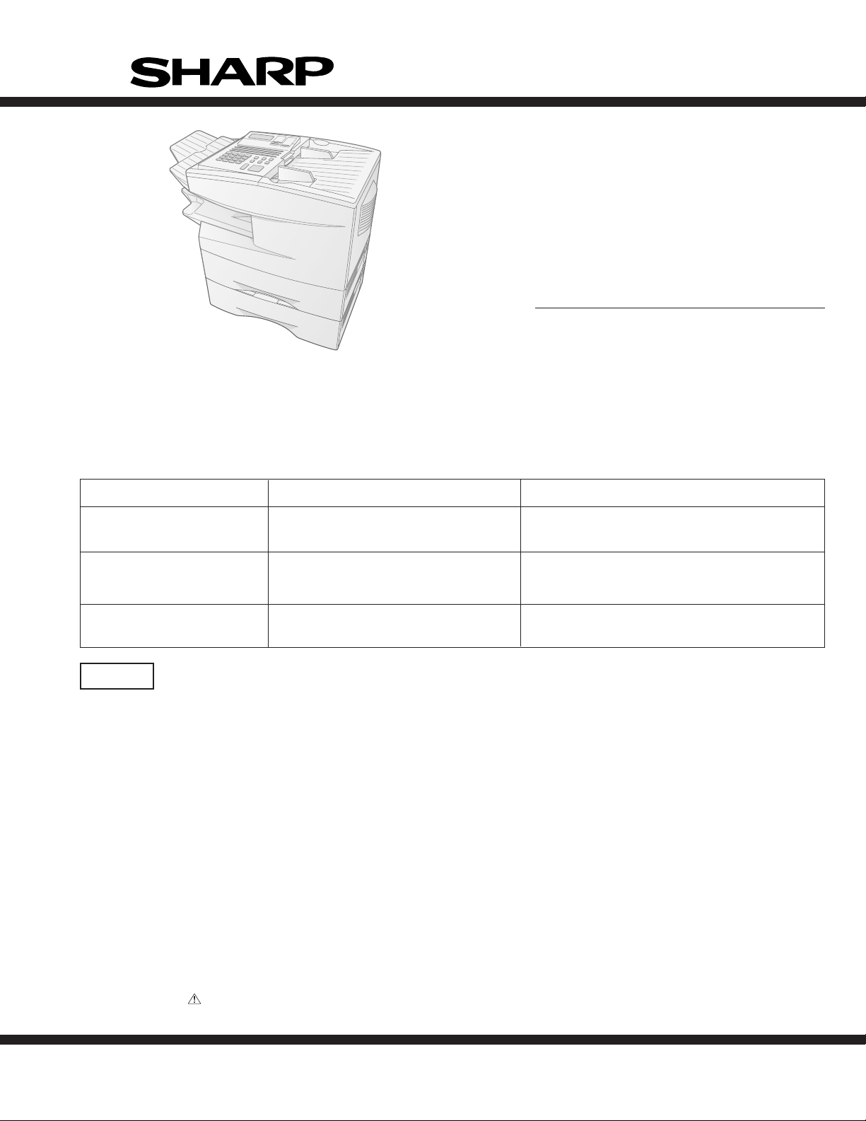
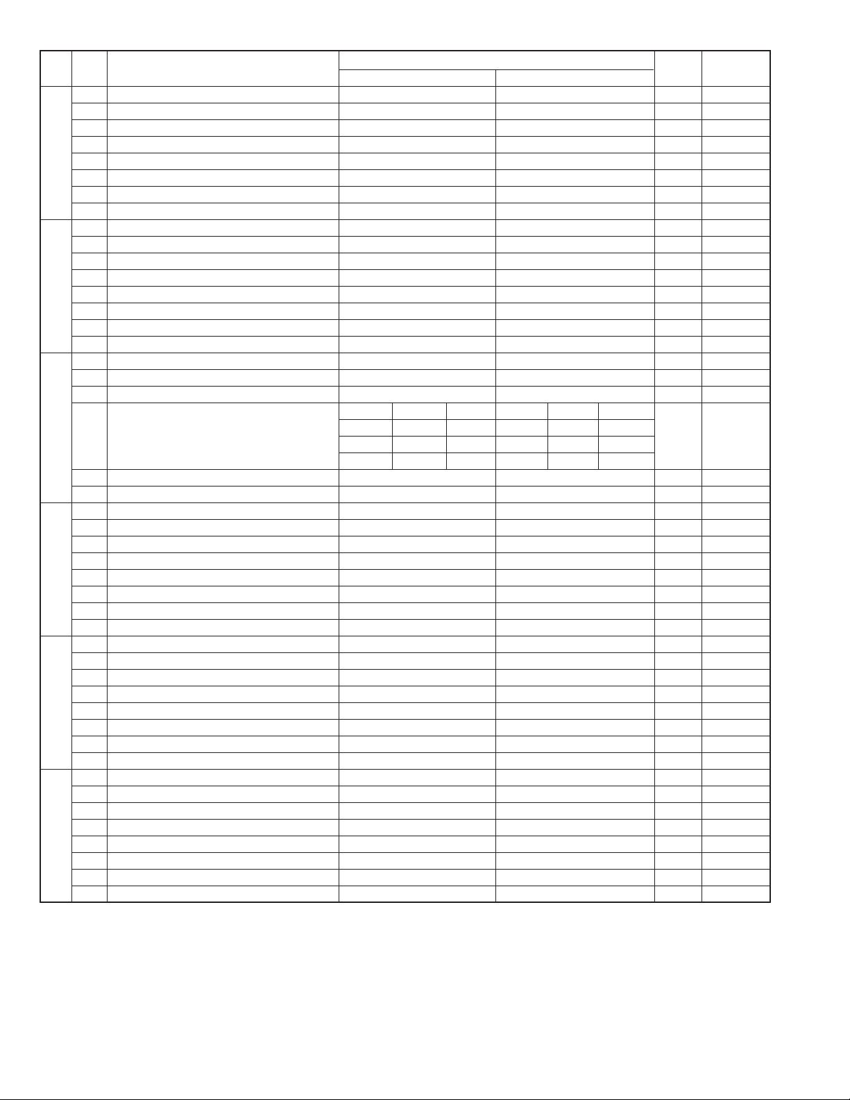
Illustration: FO-5800
In this Service Manual for FO-5800U/C which is provided with 3rd. cassette and memory PWB (FO-1MK), only the
information which differs from that for FO-5700U/C already issed is contained. For the information not contained, refer
to the Service Manual for FO-5700U (00ZFO5700USME) or FO-5700C (00ZFO5700CSME), FO-4700U/FO-47UC
(00ZFO4700USME) or FO-4700C/FO-47UC (00ZFO4700CSME) and FO-1MK (00ZFO1MKCUSME).
Difference between FO-5700U/C and FO-5800U/C
FO-5700U/C FO-5800U/C
3rd. cassette
Control PWB unit
Printer PWB unit DCEKC470BXH01 DCEKC470BXH02
CAUTION
This laser facsimile is a class 1 laser product that complies with 21CFR 1040.10 and 1040.11 of the CDRH or IEC60825-1 standard.
This means that this machine does not produce a hazardous laser radiation. The use of controls, adjustments or performance of
procedures other than those specified herein may result in hazardous radiation exposure.
This laser radiation is not a danger to the skin, but when an exact focusing of the laser beam is achieved on the eyes retina, there is
danger of spot damage to the retina.
The following cautions must be observed to avoid exposure of the laser beam to your eyes at the time of servicing.
1) When a problem in the laser optical unit has occurred, the whole optical unit must be exchanged as a unit, not an individual part.
2) Do not look into the machine with the main switch turned on after removing the toner/developer unit and drum cartridge.
3) Do not look into the laser beam exposure slit of the laser optical unit with the connector connected when removing and installing
the optical system.
4) The cover of Laser Printer Unit contains the safety interlock switch.
Do not defeat the safety interlock by inserting wedges or other items into the switch slot.
Laser Wave Length : 770-810 mm
Laser Pulse Times
Laser Output Power : 0.37 mW
: 49.2 µs
–––––––––––
U: DCEKC489MXHZZ U: DCEKC282NXHZZ
C: DCEKC283NXHZZ C: DCEKC688NXHZZ
STANDARD EQUIPMENT
Parts marked with " " is important for maintaining the safety of the set. Be sure to replace these parts with specified ones for maintaining the safety and performance of the set.
This document has been published to be used
SHARP CORPORATION
for after sales service only.
The contents are subject to change without notice.
Page 2

FO-5800U/C
CAUTION FOR BATTERY REPLACEMENT
(Danish) ADVARSEL !
Lithiumbatteri-Eksplosionsfare ved fejlagtig håndtering.
Udskiftning må kun ske med batteri
af samme fabrikat og type.
Levér det brugte batteri tilbage til leverandoren.
(English) Caution !
Danger of explosion if battery is incorrectly replaced.
Replace only with the same or equivalent type
recommended by the equipment manufacturer.
Discard used batteries according to manufacturer’s instructions.
(Finnish) VAROITUS
Paristo voi räjähtää, jos se on virheellisesti asennettu.
Vaihda paristo ainoastaan laitevalmistajan suosittelemaan
tyyppiin. Hävitä käytetty paristo valmistajan ohjeiden
mukaisesti.
(French) ATTENTION
Il y a danger d’explosion s’ il y a remplacement incorrect
de la batterie. Remplacer uniquement avec une batterie du
même type ou d’un type recommandé par le constructeur.
Mettre au rébut les batteries usagées conformément aux
instructions du fabricant.
(Swedish) VARNING
Explosionsfare vid felaktigt batteribyte.
Använd samma batterityp eller en ekvivalent
typ som rekommenderas av apparattillverkaren.
Kassera använt batteri enligt fabrikantens
instruktion.
(German) Achtung
Explosionsgefahr bei Verwendung inkorrekter Batterien.
Als Ersatzbatterien dürfen nur Batterien vom gleichen Typ oder
vom Hersteller empfohlene Batterien verwendet werden.
Entsorgung der gebrauchten Batterien nur nach den vom
Hersteller angegebenen Anweisungen.
Page 3

FO-5800U/C
CONTENTS
CHAPTER 1. GENERAL DESCRIPTION
[1] Specifications . . . . . . . . . . . . . . . . . . . . . . . . . . . . . . . . . . . . . . . . . . . . . . . . . . . . . . . . . . . . . . . . . . 1-1
[2] Refer to the service manual of FO-4700U/FO-47UC or FO-4700C/FO-47UC
[3] Refer to the service manual of FO-4700U/FO-47UC or FO-4700C/FO-47UC
[4] Refer to the service manual of FO-4700U/FO-47UC or FO-4700C/FO-47UC
[5] Refer to the service manual of FO-4700U/FO-47UC or FO-4700C/FO-47UC
CHAPTER 2. ADJUSTMENTS
[1] Adjustments . . . . . . . . . . . . . . . . . . . . . . . . . . . . . . . . . . . . . . . . . . . . . . . . . . . . . . . . . . . . . . . . . . . 2-1
[2] Diagnostics and service soft switches . . . . . . . . . . . . . . . . . . . . . . . . . . . . . . . . . . . . . . . . . . . . . . . 2-2
[3] Troubleshooting . . . . . . . . . . . . . . . . . . . . . . . . . . . . . . . . . . . . . . . . . . . . . . . . . . . . . . . . . . . . . . . 2-35
[4] Error code table . . . . . . . . . . . . . . . . . . . . . . . . . . . . . . . . . . . . . . . . . . . . . . . . . . . . . . . . . . . . . . . 2-36
CHAPTER 3. MECHANICAL DESCRIPTION
[1] Refer to the service manual of FO-4700U/FO-47UC or FO-4700C/FO-47UC
[2] Refer to the service manual of FO-4700U/FO-47UC or FO-4700C/FO-47UC
[3] Refer to the service manual of FO-4700U/FO-47UC or FO-4700C/FO-47UC
[4] How to install the verification stamp (FO-45VS) refer to the service manual supplement of
FO-4700U/FO-47UC or the service manual of FO-4700C/FO47UC
CHAPTER 4. DIAGRAMS
[1] Block diagram . . . . . . . . . . . . . . . . . . . . . . . . . . . . . . . . . . . . . . . . . . . . . . . . . . . . . . . . . . . . . . . . . 4-1
[2] Wiring diagram . . . . . . . . . . . . . . . . . . . . . . . . . . . . . . . . . . . . . . . . . . . . . . . . . . . . . . . . . . . . . . . . . 4-2
[3] Point-to-point diagram and connector signal name . . . . . . . . . . . . . . . . . . . . . . . . . . . . . . . . . . . . . 4-3
CHAPTER 5. CIRCUIT DESCRIPTION
[1] Circuit description . . . . . . . . . . . . . . . . . . . . . . . . . . . . . . . . . . . . . . . . . . . . . . . . . . . . . . . . . . . . . . . 5-1
[2] Circuit description of control PWB . . . . . . . . . . . . . . . . . . . . . . . . . . . . . . . . . . . . . . . . . . . . . . . . . . 5-1
[2-1] Circuit description of memory PWB . . . . . . . . . . . . . . . . . . . . . . . . . . . . . . . . . . . . . . . . . . . . . . 5-19
[2-2] Circuit description of 3rd. cassette PWB . . . . . . . . . . . . . . . . . . . . . . . . . . . . . . . . . . . . . . . . . . . 5-20
[3] Refer to the service manual of FO-4700U/FO-47UC or FO-4700C/FO-47UC
[4] Refer to the service manual of FO-4700U/FO-47UC or FO-4700C/FO-47UC
[5] Refer to the service manual of FO-4700U/FO-47UC or FO-4700C/FO-47UC
[6] Refer to the service manual of FO-4700U/FO-47UC or FO-4700C/FO-47UC
CHAPTER 6. CIRCUIT SCHEMATICS AND PARTS LAYOUT
[1] Control PWB circuit . . . . . . . . . . . . . . . . . . . . . . . . . . . . . . . . . . . . . . . . . . . . . . . . . . . . . . . . . . . . . 6-1
[2] LIU PWB circuit . . . . . . . . . . . . . . . . . . . . . . . . . . . . . . . . . . . . . . . . . . . . . . . . . . . . . . . . . . . . . . . 6-19
[3] Printer PWB circuit . . . . . . . . . . . . . . . . . . . . . . . . . . . . . . . . . . . . . . . . . . . . . . . . . . . . . . . . . . . . . 6-21
[4] Power supply PWB circuit . . . . . . . . . . . . . . . . . . . . . . . . . . . . . . . . . . . . . . . . . . . . . . . . . . . . . . . 6-25
[5] Operation panel PWB circuit . . . . . . . . . . . . . . . . . . . . . . . . . . . . . . . . . . . . . . . . . . . . . . . . . . . . . 6-27
[6] High voltage PWB circuit . . . . . . . . . . . . . . . . . . . . . . . . . . . . . . . . . . . . . . . . . . . . . . . . . . . . . . . . 6-29
[7] Toner empty PWB circuit . . . . . . . . . . . . . . . . . . . . . . . . . . . . . . . . . . . . . . . . . . . . . . . . . . . . . . . . 6-31
[8] 2nd. cassette PWB circuit . . . . . . . . . . . . . . . . . . . . . . . . . . . . . . . . . . . . . . . . . . . . . . . . . . . . . . . 6-32
[9] 3rd. cassette PWB circuit . . . . . . . . . . . . . . . . . . . . . . . . . . . . . . . . . . . . . . . . . . . . . . . . . . . . . . . . 6-34
[10] Memory PWB circuit . . . . . . . . . . . . . . . . . . . . . . . . . . . . . . . . . . . . . . . . . . . . . . . . . . . . . . . . . . . 6-36
CHAPTER 7. OPERATION FLOWCHART
[1] Refer to the service manual of FO-4700U/FO-47UC or FO-4700C/FO-47UC
[2] Refer to the service manual of FO-4700U/FO-47UC or FO-4700C/FO-47UC
CHAPTER 8. OTHERS
[1] Refer to the service manual of FO-4700U/FO-47UC or FO-4700C/FO-47UC
[2] Refer to the service manual of FO-4700U/FO-47UC or FO-4700C/FO-47UC
P ARTS GUIDE
Page 4

FO-5800U/C
CHAPTER 1. GENERAL DESCRIPTION
[1] Specifications
• GENERAL
Automat ic dialing Rapid Key Dialing: 48 numbers
Speed Dialing: 100 numbers
Memo ry siz e* 2 MB (approx. 116 pages)
Mode m speed 33,600 bps (max.)
Automatic fallback to lower speeds.
Transmission time* Approx. 2 seconds
Toner ca rtridge yield Initial starter cartridge (included with
(4% page coverage,letter fax machine): Approx. 3000 pages
paper) Replacement cartridge (FO-47ND):
Approx. 6000 pages
Drum car tridge yield Initial starter cartridge (included with
fax machine): 20,000 pages (avg.)
Replacement cartridge (FO-47DR):
20,000 pages (avg.)
Resolution Horizontal: 203 pels/inch (8 pels/mm)
Vertical:
Standard: 98 lines/inch (3.85 lines/mm)
Fine /Halftone:
196 lines/inch (7.7 lines/mm)
Super fine:
391 lines/inch (15.4 lines mm)
Automatic do cument 50 pages max. (20 lb letter paper)
feeder
Effective Scanning width 10.1" (256 mm) max.
Effectiv e Printing width 8.0" (203 mm) max.
Recepti on mo de s Auto/Manual
Instascan speed 30 ppm (letter paper)
Full Dual Access Yes
Copy function Single/Multi/Sort (99 copies/page)
Power requirements 120 V AC, 60 Hz
Operating temperature 50 - 86°F (10 - 30°C)
Humidity 20 to 85% RH
Power consumption Standby: 13.5 W
Maximum: 580 W
Dimensions Width: 18.1" (460 mm)
Depth: 15.2" (385 mm)
Height: 20.1" (510 mm)
Weight Approx. 54.2 Ibs.(24.6kg)
* Based on ITU-T (CCITT) T est Chart #1 at standard resolution in Sharp
special mode, excluding time for protocol signals (i.e., ITU-T phase C
time only).
Paper capacity 1250 sheets (one 250 sheet tray and
two 500 sheet cassettes)
Compression scheme MMR, MR, MH, Sharp (H2)
Halftone (grayscale) 64 levels
Applicable telephone line Public switched telephone network
Compatibility ITU-T (CCITT) G3 mode
Printing resolution Horizontal: 406 lines/inch
(16 lines/mm)
Vertical: 391 lines/inch
(15.4 lines/mm)
PC Printing: 600 dpi
Input document size Automatic feeding:
Width: 5.8 to 10.1" (148 to 256 mm)
Length: 5.0 to 14.3" (128 to 364 mm)
Manual feeding:
Width: 5.8 to 11.0" (148 to 279 mm)
Length: 5.0 to 17.0" (128 to 432 mm)
Note: This facsimile machine is Year 2000 compliant.
Option
Toner cartridge
Drum cartridge
PC interface
Option memory
Verification stamp
: FO-47ND
: FO-47DR
: FO-47IF
: FO-3MK
: FO-45VS
<IMPORTANT PLEASE READ FIRST>
To avoid problems with supplies, please don’t use supplies from other units. Please use new supplies, when supply changes are required.
1 – 1
Page 5
FO-5800U/C
TOP VOID LABEL
CHAPTER 2. ADJUSTMENTS
[1] Adjustments
General
Since the following adjustments and settings are provided for this model,
make adjustments and/or setup as necessary.
1. Adjustments
Adjustments of output voltage (FACTORY ONLY)
1. Install the power supply unit in the machine.
2. Set the recording paper and document.
3. When the document is loaded, power is supplied to the output lines.
Confirm that outputs are within the limits below.
Output voltage settings
CONTROL
PWB
CN5
12
POWER SUPPLY
PWB
Output Voltage limits
+5V MAIN 4.845V~5.355V
+5V SUB 4.845V~5.355V
+24V MAIN 23.04V~24.96V
+24V SUB 23.04V~24.96V
Connector CN4
No.
Pin No. CN1
1 11 +5V
2 10 HV C HL
39T VR
4 8 T REM
5 7 T MON
6 6 B MON
7 5 B VR
8 4 C REM
9 3 C MON
10 2 MG
11 1 +24
1
8
1
CN1
12
1
CNPW
1
CNPRT
30
1
11
1
30
CN1
1
CN4
PRINTER
PWB
–
1
8
CN7
11
CN1
HI VOLTAGE
PWB
IC2
Voltage for adjust
IC2
VR1
VD
+ Check point for voltage
+–
Digital multi meter
Fig. 1
Connector CN5
No.
Pin No. CNPW
1 +24V SUB
2MG
3MG
4MG
5 +24V MAIN
6 +24V MAIN
7 +5V SUB
8DG
9DG
10 DG
11 +5V MAIN
12 +5V MAIN
Connector CN1
No.
Pin No. CN7
1 24 MAIN
2MG
3DG
4 5V MAIN
5 HEATER ON
6FAN
7 FAN LOCK
8 H RELAY OFF
ADJUST VOLT AGE LIST
Top Void Printer Adjust V oltage
Label (mm.) Fig. 2 VR1 Fig. 1
5.5~6.9 4.42V
7.0~8.9 3.87V
9.0~10.9 3.14V
11.0~12.9 2.50V
Fig. 2
13.0~14.9 1.86V
15.0~17.0 1.22V
2. IC protectors replacement
ICPs (IC Protectors) are installed to protect the TX motor drive circuit
and verification stamp drive circuit. ICPs protect various ICs and electronic circuits from an overcurrent condition.
The location of ICPs are shown below:
12
1
27 25
CNPW
CNOP
150
130
CNPRT
IC7
F101
CNTXM
CNSTP
11
42
F100
1
1
CNLIU
CONTROL PWB
(BOTTOM SIDE)
CNPN
24
CNCIS
9
CNSP
CNSEN
101
1
2
1
8
Fig. 3
(1) F100 (ICPS10) is installed in order to protect IC’s from and
overcurrent generated in the verification stamp drive circuit. If F100
is open, replace it with a new one.
(2) F101 (ICPS18) is installed in order to protect IC’s from an overcurrent
generated in the TX motor drive circuit. If F101 is open, replace it
with a new one.
In addition to the replacement of F101 and F100, the factor causing
F101 and F100 to open must also be repaired. If not, F101 and
F100 will open again.
Replacement parts
ICPS10 (Sharp code: VHViCPS10//-1)
ICPS18 (Sharp code: VHViCPS18//-1)
3. Settings
(1) Dial mode selector
OPTION SETTING: DIAL MODE (Soft Switch No. SW2 DATA No. 1)
Use this to set the fax machine to the type of telephone line you are on.
• The factory setting is "TONE".
(step 1) Select "OPTION SETTING".
KEY:
DISPLAY:
(step 2) Select "DIAL MODE".
KEY:
DISPLAY:
(step 3) Select, using "1" or "2".
KEY:
DISPLAY: TONE SELECTED
KEY:
DISPLAY:
(step 4) End, using the "STOP" key.
KEY:
FUNCTION 4
4:OPTIONAL SETTING
ENTER #(01-34, ,#)
2
2
DIAL MODE
1
2
PULSE SELECTED
STOP
Cursor
When initially registering,
the mode shows 1=TONE.
When registering again, the
mode which was registered
formerly is shown.
1=TONE, 2=PULSE
2 – 1
Page 6
FO-5800U/C
[2] Diagnostics and service soft switches
1. Operating procedure
Two kinds of diagnoses are supported.
1-1. Fax diagnosis
This diagnosis is concerned with the main body of fax which is used
for production and service support.
Entering the diagnostic mode
FUNC
Press
display will appear.
U: ROM: FBN0
C: ROM: FBP0
FBN0
FBP0
Then press the
and the key or select with the rapid key.
Enter the mode with the
(Diag
•
specifications)
FUNC
02 PRINT AREA
03 ROM & RAM CHECK
04 AUTO FEEDER MODE
05 AGING MODE
06 PANEL CHECK MODE
07 OPTICAL ADJUST MODE
08 PRODUCT CHECK
09
10
9 8
START
key. Select the desired item with the
START
key.
9 8 7
START01 SOFT SWITCH MODE
START
START
START
START
START
START
START
START
START
U: ROM:
C: ROM:
START
SIGNAL SEND MODE
COMM. CHECK MODE
FBN0
FBP0
7
, and
the
following
key
1-2. Print diagnosis
This diagnosis is concerned with the print which is used for
production and service support.
Entering the diagnostic mode
FUNC
Press
display will appear.
PCU ROM Ver.:
Then press the
key andthe key orselect withthe rapid key.
Enterthe modewith the key.
(Diag•specifications)
FUNC
01
02
03
08
09
9 8
START
9 8 6
START
START
START
START04
START05
START06
START07
START
START
START10
START11
6
, and
key. Select the desired item with the
START
PCU ROM Ver.:
START
AREA PRINT MODE
CHECK PATTERN 1
CHECK PATTERN 2
CHECK PATTERN 3
PAPER FEED AGING
BIAS ADJUST MODE
LIFE SET MODE
LIFE ALL CLEAR
LIFE ENTRY MODE
TOP ADJUST MODE
LIFE CLEAR MODE
the
following
11
12
13
14
15 CONF. PASSCODE
16
17
18
19
20
21
22
START
START
START
START
START
START
START
START
START
START
START
START
MEMORY CLEAR
FLASH MEMORY
ALL FAX/TEL. ENTRY MODE
DEPT. PASSCODE
PRINT HOLD CODE
MEMORY SET MODE
STAMP AGING
DIAL TEST MODE
COPY DIAG MODE
SIGNAL SEND MODE2
JBIG TEST MODE
Memory clear when power is turned on
Pressing the START and STOP keys, turn on the main power, and the
following message will be displayed.
MEMORY CLEAR
EXECUTE ? 1 = YES , 2 = NO
Here, when 1: YES is selected, the memory will be cleared to be ready
for operation.
If 2: NO is selected, it will continue ready for operation as it is.
2 – 2
Page 7
FO-5800U/C
2. Diagnostic items description
2-1. Fax diagnosis
1) Soft switch mode
In this mode, the soft switch are set and the soft switch list is printed.
Soft switch mode screen
S O F T S W I T C H M O D E
S W 0 1 = 0 0 0 0 0 0 0 0
8
Data
1
Switch number selection
1 2 3 4 5 6 7 :DATA No.
Switch
No.
• Press START key for setting of the next soft switch. If the soft
switch number is the final, pressing START key will exit the soft
switch mode.
• Enter two digits of a soft switch number to set the switch number.
If a switch number of unexisting soft switch is entered, key error
buzzer sounds to reject the input.
S O F T S W I T C H M O D E
S W 0 1 = 0 0 0 0 0 0 0 0
2
Data number selection
E N T E R L A S T D I G I T
S W 1
1 6
S O F T S W I T C H M O D E
S W 1 6 = 0 0 0 1 0 1 1 0
The cursor position shows the data to be set.
Pressing # key moves the cursor to the right. If, however, the cursor is
on data number 8, pressing # key shifts the cursor to data number 1
of the next switch number. If the switch number is the final, pressing
# key will exit the soft switch mode.
Pressing key moves the cursor to the left. If, however, the cursor is
on data number 1, pressing key shifts the cursor to data number 1
of the former switch number. If the switch number is 1, pressing
key will not move the cursor and the error buzzer will sound.
3
Data setting method
Press the FUNCTION key, and the data at the position of the cursor
will be reversed to 0 when it is 1, or to 1 when it is 0. (If the soft switch
can be changed at the bit (Refer to 6.), the error buzzer will sound
with the process not received.)
4
Outputting method of soft switch list
In the soft switch mode, press the REPORT key, and the soft switch
list will be output.
If the recording paper runs out or is clogged, the key error buzzer will
sound with the process not received.
5
Storage of data
In the following case, the data of the soft switches set will be stored.
• It is shifted to set the next soft switch by pressing the START
switch.
• It is shifted to set the next soft switch with the [#] key.
• It is shifted to set the last soft switch with the [ ] key.
• It is shifted to set another soft switch by inputting two digits as the
switch number. (When 2 digits are completely input.)
• Output of the soft switch list is started.
6
Inhibition of data change
(This is also applicable for the optional setting.)
In the following case, it is inhibited to change the data with the key
error buzzer.
• Switching ON/OFF of ECM during the use of image memory.
• Switching OFF to ON of the print hold function when the print
hold pass code has not yet been registered.
• Clearing the print hold pass code when print hold function is ON.
• Switching ON/OFF of the print hold function during the use of
memory such as in the case of substitute receiving.
• OFF to ON of telephone billing function which is using the image
memory is used (Note: In the existing set, the telephone billing
code function is specified from OFF to ON when the timer system
communication (including the batch communication) is set.)
Here, the memory is usable when the telephone billing code function is on. It can be set from ON to OFF while the memory is
used. However, if setting is practically changed even once, it can
not be returned from OFF to ON.
• Switching ON/OFF of PC interface function during the use of im-
age memory.
• OFF to ON of department control function during use of image
memory.
(Note: In the existing set, the department control function is set
from OFF to ON when the timer communication (including the
batch sending) or the memory hold is set.)
• ON to OFF of continuous serial polling function when the con-
tinuous serial polling is started.
(Note: In the existing set, "ON to OFF of the continuous serial
polling function when the continuous serial polling is registered"
has been applied, but the conditions are now moderated. However, registration is impossible to the program of the new continuous serial polling when the continuous serial polling function is
OFF.)
• In addition, change of all soft switches during communication
7
Linked change of data (This is the same even in the optional setting.)
• When the department control function is off, the multi TTI func-
tion and telephone billing code function are turned off.
2) Print area
According to the size of the specified sheet, the effective printing area is
printed.
3) ROM & RAM check
The sum value of ROM, the work and the back-up RAM are checked.
The RS232C interface is also checked. If any error occurs, the buzzer
will inform it. (Refer to the following table). Finally, the result will be printed.
This diagnosis does not check the flash memory. The flash memory is
checked with the flash memory test.
Number of buzzer sounds Device checked Remarks
1 time <Short sound> ROM Main
2 times <Short sounds> Integrated ROM Main
3 times <Short sounds> SRAM Main
4 times <Short sounds> DRAM Main
For the short and long sounds, one pattern is as follows.
Main system: 0.5 seconds ON/0.5 seconds OFF
Sub system: 1.00 second ON/0.5 seconds OFF
The execution state of checking is as follows. Moreover, the list of the
check result is output after checking is ended.
Display during check
ROM CPU SRM DRM
• • • •
Display after check
ROM CPU SRM DRM
P P P E
P=PASS E=ERROR
ROM/RAM
check list
output
2 – 3
Page 8
FO-5800U/C
4) Auto feeder mode
The auto feed function can be checked by inserting and discharging the
document. (The distance between pages can be displayed during operation of the scanner.)
1
Check of auto feed function
After this mode is activated, set up the document, and press the
STAR T key , and it will be automatically fed. (Before the ST ART key is
pressed, the document sensor alone is activated.) Moreover, the
document size (A4/B4) and sensor information (A4/B4/ORG) are displayed when the document sensor is turned.
04 : AUTO FEEDER MODE
After setup of the document
04 : AUTO FEEDER MODE
B4 (A4 B4 ORG)
Only the sensor which is
activated (fallen down) is displayed.)
The paper sheet size (A4/B4) is
displayed.
2
Display of distance between pages during operation of the scanner
• Soon after this mode is activated, press the FUNCTION key for 5
seconds or more, and the display mode of the distance between
pages will be activated. Then, set up the sending paper and select
the image quality, and then press the START key, and operation
will be started.
Be sure to press the FUNCTION key prior to the START key. If
the FUNCTION key is not pressed but the STAR T key is pressed,
it will operate in the same matter as in the existing auto feeder
mode.
If the START key is pressed, the FUNCTION key will be invalid
hereafter. Therefore, the display mode of the distance between
pages and the existing mode can not be changed.
• While the sending paper is read, the image quality key can be
input. STD/FINE/S-FINE modes are usable. However, the same
operation of FINE will be selected if the intermediate tone is set.
• The image quality, the length of the sending page read, the page
distance to the next sending paper and the total of the sending
papers read are shown on the display.
• When the stop key is pressed or 100 sending papers are read,
the content shown on the display will be totally output as the list
after the remaining sending papers are discharged.
5) Aging mode
If any document is set up in the first state (when started), copying will be
executed. If it is not set up, "check pattern 1" of the print diagnosis is
output at the intervals of 1 time/60 minutes. (A total of 10 sheets are
output.)
7) Optical adjust mode
Set documents and press the START key for ordinary copying.
According to key operation, copying can be temporarily stopped.
STOP key: To temporarily stop reading documents.
START key: To start reading documents again.
When any document is not set, print area printing is performed.
8) Product check
The diagnosis is used in the production process.
After shift to the mode, the following operations are sequentially executed. At this time, the sensor of read-error can be checked by feeding
the B4 document. Set up one short document of B4 size.
1
Memory clear (Same as Diagnosis 11)
2
Panel test (Same as Diagnosis 06)
3
Dial test (Same as Diagnosis 24)
4
Document auto feed
5
ROM & RAM test check (Same as the Diagnosis 03)
6
Flash memory test mode (Same as Diagnosis 12)
7
Registration of fixed data
Registration of rapid key No. and other data necessary for produc-
tion.
The registered data are shown in the following table. The chain dial
is not set for any destination.
Rapid FAX Rapid FAX Rapid FAX Rapid FAX
No. No. No. No. No. No. No. No.
01 20 06 25 11 1 21 01
02 21 07 26 12 2 22 02
03 22 08 27 13 3 23 03
04 23 09 28 14 4 24 04
05 24 10 29 15 5 25 05
8
Transmission check (Same as Diagnosis 10)
The soft switches necessary for production are set.
9
Test result print (one sheet)
Memory clear printing
Panel test result printing
ROM & RAM test result printing
F
Print area printing (one sheet)
6) Panel check mode
This is used to check whether each key is normally operated or not.
According to the key input, LCD is displayed. Moreover, during execution,
the document reading lamp is turned on.
T est results are printed. (The maximum 100 input keys can be printed .)
LED repeats lighting at regular intervals in sequence. (Lighting speed
is specified separately.)
In case of inputting all keys, key input OK is displayed when finishing
the STOP key.
When pressing the NUMERIC key during panel check, output of DTMF
corresponding with the key is started.
When pressing other keys, output is stopped.
2 – 4
Page 9

9) Signal send mode
Rapid key RXX XX : Rapid number
SPEED key SXXX XXX
: Speed key number
After shift to the mode, press the START key, and the signals will be
transmitted in the following sequence.
It can be used to check the modem and so on.
[ 1] No signals
[ 2] 4800BPS (V27ter)
[ 3] 14400BPS (V . 33)
[ 4] 12000BPS (V . 33)
[ 5] 14400BPS (V . 17)
[ 6] 12000BPS (V . 17)
[ 7] 9600BPS (V. 17)
[ 8] 7200BPS (V. 17)
[ 9] 9600BPS (V. 29)
[10] 7200BPS (V . 29)
[11] 4800BPS (V27ter)
[12] 2400BPS (V27ter)
[13] 300BPS (FLAG)
[14] 2100Hz (CED)
[15] 1100Hz (CNG)
10) Comm. check mode
Turn on the line monitor .
1
2
Turn off the COVER SHEET FUNCTION.
3
Set line equivalence at 0 km.
After the check, it is necessary to be sure to return the aforementioned
soft switches into the initial state.
(Clear the memory with the diagnosis.)
11) Memory clear
Clear the back-up memory to initialize the soft switches.
The flash memory will be initialized. Then, the initialized list be output.
12) Flash memory
The flash memory is checked.
The ordinary memories (ROM, SRAM, DRAM) are checked in the ROM
& RAM check process. The write/read test is taken every block to print
the result.
When an error occurs, the following error buzzer will sound.
Number of buzzer sounds Check device
9 times <Short sounds> Flash memory (Option)
During operation of this diagnosis, dual operation is not possible at all.
If this is excessively repeated, it will shorten the life of the flash memory.
13) All FAX/TEL. entry mode
The function is used to simplify the registration of FAX/TEL No. during
aging.
1
The diagnosis mode is activated. If anything is not registered in the
Rapid number 01 or any program or group is not registered, it will
pass the diagnosis without doing anything.
2
The FAX/TEL number (including the substitutive destination) of the
Rapid number 01 is copied to the Rapid numbers 02 thru 48.
3
FAX number of the Rapid number 01 is copied to SPEED key numbers
001 thru 200.
FO-5800U/C
4
If any chain dial is not in the Rapid number, the Rapid numbers 02
thru 48 and SPEED key numbers 001 thru 200 are registered in the
group number 01.
If any chain dial is set, the group will be not produced but the chain
dial setting alone of the Rapid number 01 will be reset.
(In all others except the Rapid number 01, the chain dials will be
continuously set as they are.)
(16th and subsequential letters of the destination name registered in the
Rapid number 01 will be discarded.)
14) Dept. passcode
The department passcode list is printed.
15) Conf. passcode
The confidential passcode list is printed.
Differing from printing of one box alone soon after registration, the confidential passcodes of all boxes are printed.
16) Print hold code
The print lockout passcode No. is printed.
17) Memory set mode
The set and dump list of the memory content is output.
• The address (8 digits (P) generally including the bank information is
input, and the data of 2 digits is continuously input.
Inputting is done in the hexadecimal mode. The ten-key is used for 0
thru 9, and the alphabetic keys A (RAPID 01 thru 06) are used for A
thru F.
• During data inputting, the address can be moved forward and back-
ward one byte by one byte with " " and "#". (The address prior to the
address 0 is looped as the maximum address.)
• The V alidity of the address is not checked. Accordingly, writing/ read-
ing operations are possible in the address of the memory not as-
signed, the address of ROM and so on.
(However, as practical, writing is not done, and the data content runs
short each reading.)
Though writing is possible in the flash memory, a little time is re-
quired.
It is also necessary to take care that the life of the flash memory is
excessively shortened if much data is written in the flash memory.
Since it may run away depending the written content, take minute
care for the writing address.
• When the REPORT key is input, the memory dump list is produced
from the displayed address (here, it is limited at the 16-byte bound-
ary address (address with end 0) which does not exceed the speci-
fied address and is just in front.). The dump list is output to a maxi-
mum of 99 pages. If any data of one page can be repeatedly devel-
oped and printed, the list is sufficient. But it is not desired that the
content of plural pages are developed in the memory once and are
then printed. If the STOP key is pressed, it will pass to the diagnosis
after the page which is now being printed is completed printed.
If the address exceeds the maximum address, it will return to the
address 0 and printing will be continued.
18) Stamp aging
Diag mode is left though it doesn’t have this function.
2 – 5
Page 10

FO-5800U/C
19) Dial test mode
The mode is used to inspect whether dialing is accurate in two kinds of
dial modes . All data which can be dialed in this mode are automatically
called up in both PB mode and DP mode.
When this mode is activated, the following operations will be automatically executed . Whether the dialed content is right or not is judged with
the external instrument which is connected to the line cable.
1
After shift to the FAX diagnosis mode, press RAPID 24.
(Also switch the display with the [ ] and [#] keys.)
2
Press the START key.
3
Turn on CML, and dial the following in the PB mode.
1, 2, 3, 4, 5, 6, 7, 8, 9, , 0, #
4
Turn off CML 500 mS alone.
5
Dial the following in the DP mode.
1, 5, 9, 0
6
After dialing, turn off CML.
This mode uses the ordinary auto dial. (Accordingly, the signal sending
time and minimum pause are all the same as ordinary.
The measurement result in this mode is completely all the same as in
the ordinary dial mode.
Moreover, the same process as above is also done in the dial test mode
which is executed in the product check mode.
20) Copy diag mode
In order to shorten the process time during production, this mode is
used to automatically switch the copy mode. Three menus are provided.
1. 1Set up two documents. (In case of two documents or more,
there is no problem.
2
Press the STAR T key.
3
Copy 1st document in the fine mode/density AUTO. (One sheet
is printed in the ordinary copy mode.)
4
Copy 2nd (subsequential) document in the intermediate tone
mode/density DARK. (In the ordinary copying mode, one sheet
is printed when the RESOLUTION key is pressed three times.)
When copy test is tried during production or is checked in two modes
(fine and intermediate tones), this mode is provided to reduce the troublesome work which makes the operator stand aside to change the mode.
Accordingly, the fine and intermediate tones are merely switched, and
the mode is not switched to another mode. (Input of the image quality/
density key is invalid.)
2. Try the copy in the mode fixed at COPY REDUCE 95% and fine
mode/density AUTO. At this time, don’t change the soft key of
COPY REDUCE. (Input of the image quality/density key is invalid.)
3. Continuously try the above items 1 and 2.
21) Signal Send Mode2
The signals concerned with V.34 & V.8 are checked.
After this mode is activated, press the START key, and the signals will
be sent in the following sequence.
It can be used to check the modem.
[ 1] No signal
[ 2] 33600BPS
[ 3] 31200BPS
[ 4] 28800BPS
[ 5] 26400BPS
[ 6] 24000BPS
[ 7] 21600BPS
[ 8] 19200BPS
[ 9] 16800BPS
[10] 14400BPS
[11] 12000BPS
[12] 9600BPS
[13] 7200BPS
[14] 4800BPS
[15] 2400BPS
22) JBIG Test Mode
Enter the diagnostic mode.
1
2
Press the RAPID22 button. ("22: JBIG TEST MODE" appears.)
3
Press the START key to begin the JBIG test operation.
When both tests are completed normally, the buzzer sounds and "JBIG
TEST NORMAL END" appears at the same time.
If the decoding test terminates abnormally, the buzzer sounds and
"ERROR: JBIG DECODE" appears at the same time.
If the encoding test terminates abnormally, the buzzer sounds and
"ERROR: JBIG ENCODE" appears at the same time.
2 – 6
Page 11
FO-5800U/C
2-2. Print diagnosis
Rapid key 01: Area print mode
The effective printing area frame is printed in the specified sheet size.
1
2
3
4
5
6
7
8
9
4mm ± 2
208mm
1. [Full black pattern]
2. [Intermediate tone 2 pattern]
3. [Intermediate tone 1 pattern]
4mm ± 2.5
4mm
4mm
The left pattern is repeated.
The left pattern is repeated.
Rapid key 05: Paper feed aging
The mode is used for aging related to the printing. In this mode, the
following modes are provided.
1
Blank paper aging mode (ALL WHITE AGING)
2
Whole black print aging mode (ALL BLACK AGING)
3
4% printing aging mode (4% AGING)
After selecting the paper-pass aging mode in the print diagnosis mode,
input the number of each mode above with the ten-key, and the mode
will be executed. The detailed specifications of each mode are described
as follows. Here, the operation in each mode is stopped only when the
STOP key is pressed by the operator or a printing-impossible error occurs.
• Blank paper aging mode
In the mode, printing is continued in the whole white (white paper)
printing pattern until the STOP key is pressed by the operator . (In the
printing area)
• Whole black printing aging mode
In the mode, printing is continued in the whole black (whole black)
printing pattern until the STOP key is pressed by the operator . (In the
printing area)
Rapid key 06: Bias adjust mode
The mode is used to adjust the printing density of the printed image. The
image printing density is adjustable in seven steps of 1 to 7.
For details, refer to the following table. (For selection, use the keys 1
thru 7.)
Image printing density Thin ←→Thick
1234567
Default value
4. [Mesh point pattern]
The left pattern is repeated.
5. [Longitudinal strip 2 pattern]
Black 2 dot and white 2 dot are repeated in line.
6. [Lateral strip 2 pattern]
Black 2 line and white 2 line are repeated.
7. [Longitudinal strip 1 pattern]
Black 1 dot and white 1 dot are repeated in line.
8. [Lateral strip 1 pattern]
Black 1 line and white 1 line are repeated.
9. [Full White pattern]
Rapid key 02: Check pattern 1
The lateral stripe 2 pattern is printed on one sheet.
(Black 2 line and white 2 line are repeated.)
Rapid key 03: Check pattern 2
The lateral stripe 2 pattern is printed on multiple pages.
Press the STOP key to end the printing.
Rapid key 04: Check pattern 3
The intermediate tone 1 is printed on one sheet.
Rapid key 07: Life set mode
The mode is used to set the life counter of the printer and the counter of
the auto feeder at desired values. For setting, proceed with the following
procedure.
1
When the life counter setting mode is selected, the following will be is
displayed.
= 00123
DRUM
LIFE
LIFE
IFE1
L
LIFE2
LIFE3
0
= 00123
0
= 00123
0
= 00123
0
= 00123
0
0
key
MACHINE
# key
FEEDER LI FE = 00123
The cursor blinks at the top data.
Five counters can be selected with the "#" and " " keys.
2
In the state 1, input a desired setting number of 6 digits with the tenkey.
3
After input of 6 digits, shift to another counter with the "#" and " "
keys as necessary. When all necessary counters are completely input, press the START key.
4
"STORED" will be displayed with the set values stored into the memory.
For checking, retry this mode.
Note:
This counter indicates the printer use conditions such as numbers of
printed pages from the beginning of use. In the normal memory clear
condition, the counter will not be reset.
In conditions including damaged memory contents caused by repairing
the panel, this counter should be reset or cleared in addition to the ordinary memory clear.
2 – 7
Page 12
FO-5800U/C
Rapid key 08: Life all clear
The mode is used to clear the life counter of the printer of the counter
of the auto feeder.
Note: The counter shows the operational state of the printer (e.g. how
many sheets have been printed since start of use?). The ordinary memory does not reset the counter. Accordingly, it is necessary to reset this counter in addition to the ordinary memory
clear if the content in the memory on the control PWB is broken
because of PWB repair, etc. (In the production stage, it is necessary to execute this in the last process.)
Rapid key 09: Life entry mode
(For Serviceman temporary counter)
The mode is used to set a desired value for the judgment value (alarm
judgment counter value) of the general purpose life counters 1 thru 3 of
the printer. If the life of a consumable part (developer, imprinter, etc) is
set, the model which has the error display and RMS function will inform
RMS when the counter reaches the set value. For setting, proceed with
the following procedure.
1
When the life counter setting mode is selected, the following will be
displayed.
# key
LI FE1= 00000
LI FE2= 00000
0
0
key
Rapid key 11: Life clear mode
The mode is used to respectively clear the life counter of the printer and
the counter of the auto feeder. For setting, proceed with the following
procedure.
1
When the life counter clearing mode is selected, the following will be
is displayed.
Seven counters can be selected with the "#" and " " keys.
# key
MACHINE
DRUM
FEEDER L I FE LEAR
TONER L I FE LEAR
LIFE
LIFE
L
IFE1
LIFE2
LIFE3
LEAR
C
LEAR
C
LEAR
C
LEAR
C
LEAR
C
C
C
key
LI FE3= 00000
0
The cursor blinks at the top data.
Three counters can be selected with the "#" and " " keys.
2
In the state 1 , input a desired setting number of 6 digits with the ten-
key.
3
After input of 6 digits, shift to another counter with the "#" and " "
keys as necessary. When all necessary counters are completely input, press the START key.
4
"STORED" will be displayed with the set values stored into the
memory. For checking, retry this mode.
Note: The counter shows the operational state of the printer (how many
sheets have been printed since start of use? and others). The
ordinary memory does not reset the counter. Accordingly, it is
necessary to reset the counter or do the clear process in addition to the ordinary memory clear if the content in the memory
on the control PWB is broken because of PWB repair, etc. (In
the production stage, it is necessary to execute this in the last
process.)
Rapid key 10: Top adjust mode
As the method to adjust the top margin for printing, adjust top margin
adjusting VR on the PWB. If this mode is used at this time, adjustment is
possible without the printing test every time when VR is turned.
For the practical use, determine the adjusting value on the basis of the
old data, and adjust to the determined value in this mode. Then, check it
with the printing test.
2
In the state 1, input the CLEAR key, and the counter will be respectively cleared.
3
After one clear, move the cursor to another counter with the "#" and
" " keys as necessary, and then press the CLEAR key. When the
necessary counters are completely cleared, press the STOP key.
2 – 8
Page 13
3. How to make soft switch setting
To enter the soft switch mode, make the following key entries in sequence.
FO-5800U/C
Press
FUNCTION
9 8 7 START 0 1START
S F T S W 1 = 0 0 0 0 0 0 0 0
S F T S W 1 = 1 0 0 0 0 0 0 0
S F T S W 1 = 1 0 0 0 0 0 0 0
S F T S W 1 = 1 0 0 0 0 0 0 0
S F T S W 1 = 1 0 0 0 0 0 0 0
S F T S W 2 = 0 0 0 0 0 0 0 0
S F T S W 99 = 0 0 0 0 0 0 0 0
Press FUNCTION key.
Press key.
Press key.
Bit1 - 8 are set.
Press key during setting.
START
Soft SW2 - 99 are set.
To finish the settings halfway between
SW 1 and SW99, press the STOP key.
In this case, the setting being done to
the SW No. on display will be nullified
while settings done to the preceding
SW Nos. remain in effect.
The soft switch mode is terminated.
2 – 9
Page 14
FO-5800U/C
4. Soft switch description
• Soft switch
DATA
SW
NO.
NO.
1 Recall interval Binary input 8421 0 OPTION
2 No. = 1234(Data No.) 1 Set to 1~15
3 EX 0101 0
SW1
SW2
SW3
SW4 3 No. 3 1 00001
SW5
4 eg. Recall interval is set to 5 min. 1
5 Recall times Binary input 8421 0 OPTION
6 No. = 5678(Data No.) 0 Set to 0~14
7 EX 0010 1
8 eg. Recall times is set to 2 times. 0
1 Dial mode PULSE TONE 0
2 Receive mode AUTO MANUAL 1
3 ECM mode Off On 0 OPTION
4 Reserved 0
5 Polling security On Off 1 OPTION
6 Auto cover sheet No Yes 1 OPTION
7 JUNK-FAX function in manual reception Yes No 0
8 JUNK-FAX function Yes No 0 OPTION
1 Number of rings for auto-receive Binary input 8421 0 OPTION
2 (0: No ring receive) No. = 1234(Data No.) 0 Set to 0~9
3 EX 0001 0
4 eg. Number of rings for auto receive is set to 1 time. 1
5 Switch to auto-receive from manual receive Binary input 8421 0 OPTION
6 (0: No switch) No. = 5678(Data No.) 0 Set to 0~9
7 EX 0000 0
8 eg. Switch to auto receive is set to disable. 0
Communication results printout Printed at Printed at Printed at
1 No. 1 0 00110
2 No. 2 0 01010
4 Image addition function to the communication On Off 1 OPTION
result table (for memory transmission only)
5 Reserved 0
6 TEL billing code function On Off 0 OPTION
7 Billing code position Before After 1 OPTION
8 Multi-TTI feature On Off 0 OPTION
1 Time display format 24 hours 12 hours-AM/PM 0
2 Date display format Month-Day-Year Day-Month-Year 1
3 Header print Off On 0
4 Footer print On Off 0
5 Relay data output No Yes 0
6 Substitute reception Off On 0
7 Substitute reception conditions Reception disable without TSI Reception enable without TSI 0
8 CSI transmission Off On 0
ITEM
error only
Switch setting and function
1
error/timer/
memory sion mode
only only
transmis- every time
0
Not printed
Printed OPTION
Initial
setting
Remarks
2 – 10
Page 15
FO-5800U/C
DATA
SW
NO.
NO.
1 JBIG (Joint Bi-level Image Group) On Off 1
2 JBIG option On Off 0
3 MMR On Off 1
4MR On Off 1
SW6 Modem speed V.33 V.17 V. 29 V. 27ter
5 No. 5 0 0 1 1 1 1 0 0 0 0 1
6 No. 6 1 1 0 0 0 0 0 0 0 0 0
7 No. 7 0 1 0 1 0 1 0 1 1 0 0
8 No. 8 0 0 0 0 1 1 1 1 0 0 0
Reception speed fixed NO V. 17- V. 29- V. 27ter-
1 No. 1 0 1 0 1 0
2 No. 2 0 1 1 0 0
3 DIS receive acknowledge during Twice Once in NSF reception, twice 0 Effective to
G3 transmission in DIS reception international
SW7 comm.
4 Non-modulated carrier in V.29 On Off 0
transmission mode
5 CNG send in manual transmission On Off 1
6 Protocol monitor On Off 0
7 Line monitor On Off 0
8 Max. length for TX/RX/Copy TX: unlimited, RX: unlimited TX/Copy: 1.0m, RX: 1.5m 0
Compromised equalizer 0Km 1.8Km 3.6Km 7.2Km Valid when
1 No. 1 0 0 1 1 0 transmitting
2 No. 2 0 1 0 1 0
3 H2 mode No Yes 0
SW8
4 Signal transmission level Binary input 16 8 4 2 1 0
5 No. = 45678 (Data No.) 1
6 EX 01101 1
7 eg. Signal transmission level is set to -10dBm 0
8 1
ITEM
Switch setting and function
1
14400 12000 14400 12000
0
9600 7200 9600 7200 4800 2400
14400BPS 9600BPS 4800BPS
Initial
setting
Remarks
When 14400BPS
MODEM used,
setting to
14400BPS is
ignored.
2 – 11
Page 16
FO-5800U/C
SW
DATA
NO.
NO.
CED tone signal interval 75ms 500ms 750ms 1000ms
1 No. 1 0 0 1 1 0
2 No. 2 0 1 0 1 0
3 Equalization freeze On Off 0
SW9 4 Equalization freeze conditions All 7200bps 0
5 CED detection time 500ms 1000ms 0
Alarm buzzer 3sec 1sec No BEEP No BEEP
6 No. 5 0 0 1 1 0
7 No. 6 0 1 0 1 0
8 Action when RTN received Not Error Error 0
1 Memory retransmission times Binary input 8421 1 OPTION
2 No. = 1234(Data No.) 0
3 EX 1010 1
SW10
SW11
SW12
SW13
SW14
4 eg. Retransmission time set to 10 times. 0
5 Memory retransmission interval Binary input 8421 0 OPTION
6 No. = 5678(Data No.) 0
7 EX 0010 1
8 0
1 Reserved 1
2 Reserved 1
3 Reserved 1
4 Reserved 0
5 Reserved 1
6 Reserved 1
7 Reserved 1
8 Reserved 0
1 Reserved 1
2 Reserved 1
3 Reserved 0
EOL detection timer 13sec 25sec 5sec 5sec
4 No. 4 0 0 1 1 0
5 No. 5 0 1 0 1 0
Processing of DIS reception
after DIS transmission
6 No. 6 0 0 1 1 0
7 No. 7 0 1 0 1 0
8 The change to DB from DP by Yes No 0
1 DTMF output level (High) Binary input 16 8 4 2 1 0
2 No. = 45678 (Data No.) n = 0.5dBm 1
3 EX 01100 1
4 eg. Signal transmission level is set to -10dBm 0
5 0
6 Reserved 0
7 Reserved 0
8 Reserved 0
1 DTMF output level (Low) Binary input 16 8 4 2 1 1
2 No. = 45678 (Data No.) n = 0.5dBm 0
3 EX 10000 0
4 eg. Signal transmission level is set to -10dBm 0
5 0
6 Reserved 0
7 Reserved 0
8 Reserved 0
ITEM
Switch setting and function
1
Retransmitting
command
Breaking Apply to T.30+α
circuit T.30
0
Initial
setting
Remarks
2 – 12
Page 17
FO-5800U/C
SW
NO.
SW15
SW16
SW17
SW18
SW19
SW20
DAT A
NO.
1 Reserved 0
2 Reserved 0
3 Reserved 0
4 Reserved 0
5 Reserved 0
6 Reserved 0
7 Reserved 0
8 Reserved 0
1 Reserved 0
2 Reserved 0
3 Reserved 0
4 Reserved 0
Cl Signal OFF detect enable time
5 No. 5 0 0 0 0 0 0 0 0
6 No. 6 0 0 0 0 1 1 1 1
7 No. 7 0 0 1 1 0 0 1 0
8 No. 8 0 1 0 1 0 1 0 1
1 Reserved 0
2 Reserved 0
3 Reserved 0
4 Reserved 0
Distinctive ringing OFF STD
5 No. 5 0 0 1 0 1 0 1 0
6 No. 6 0 0 0 1 1 0 0 0
7 No. 7 0 0 0 0 0 1 1 0
8 No. 8 0 1 0 0 0 0 0 0
1 Reserved 0
2 Reserved 0
3 Reserved 0
4 Reserved 0
5 Reserved 0
6 Reserved 0
7 Reserved 0
8 Reserved 0
1 Reserved 0
2 Reserved 0
3 Reserved 0
4 Reserved 1
5 Reserved 1
6 Reserved 0
7 Reserved 0
8 Reserved 0
1 Reserved 0
2 Reserved 0
3 Reserved 1
4 Reserved 1
5 Reserved 0
6 Reserved 0
7 Reserved 0
8 Reserved 0
ITEM
(ms)
Switch setting and function
1
200 300 350 400 500 700 1200
RING1 RING2 RING3 RING4 RING5
0
Initial
setting
Remarks
2 – 13
Page 18
FO-5800U/C
SW
NO.
SW21
SW22
SW23
SW24
SW25
SW26
DAT A
NO.
1 Reserved 1
2 Reserved 0
3 Reserved 0
4 Reserved 0
5 Reserved 1
6 Reserved 0
7 Reserved 0
8 Reserved 0
1 Reserved 0
2 Reserved 0
3 Reserved 0
4 Reserved 0
5 Reserved 0
6 Reserved 0
7 Reserved 0
8 Reserved 0
1 Reserved 0
2 Reserved 0
3 Reserved 0
Busy tone detection frequency
4 No. 4 0 0 0 0 1 0
5 No. 5 0 0 1 1 0 0
6 No. 6 0 1 0 1 0 0
7 Reserved 0
8 Reserved 0
1 Reserved 0
2 Reserved 0
3 Reserved 0
4 Reserved 0
5 Reserved 0
6 Reserved 0
7 Reserved 0
8 Reserved 0
1 Reserved 0
2 Reserved 0
3 Reserved 0
4 Reserved 0
5 Reserved 0
6 Reserved 0
7 Reserved 0
8 Reserved 0
1 Reserved 0
2 Reserved 0
3 Reserved 0
4 Reserved 0
5 Reserved 0
6 Reserved 0
7 Reserved 0
8 Reserved 0
ITEM
Switch setting and function
1
520~640Hz 300~600Hz 380~500Hz
0
reserve reserve
Initial
setting
Remarks
2 – 14
Page 19
FO-5800U/C
SW
NO.
SW27
SW28
SW29
SW30
SW31
DAT A
NO.
1 F.A.S.T (RMS) mode On Off 0
2 Reserved 0
3 V erification ST AMP Ye s No 0
4 Summer time (Day light saving) No Yes 1
Key buzzer volume Off HIGH MIDDLE LOW
5 No. 5 0 0 1 1 1
6 No. 6 0 1 0 1 0
7 Reserved 0
8 Reserved 0
Speaker volume HIGH HIGH MIDDLE LOW
1 No. 1 0 0 1 1 1
2 No. 2 0 1 0 1 1
3 Reserved 1
4 Reserved 0
Ringer volume Off HIGH MIDDLE LOW
5 No. 5 0 0 1 1 1
6 No. 6 0 1 0 1 1
7 Reserved 0
8 Reserved 0
1 Reserved 0
2 PC I/F mode On Off 1 OPTION
3 Reserved 0
4 Reserved 0
5 Reserved 0
6 Reserved 0
7 Reserved 0
8 Reserved 0
1 Header registration On Off 0
2 Reserved 0
3 Reserved 0
4 Reserved 0
5 Reserved 0
6 Reserved 0
7 Reserved 0
8 Quick on-line function Yes No 1
Cassette selection Manual Auto-1 Auto-2 Auto-1 OPTION
1 No. 1 0 0 1 1 0
2 No. 2 0 1 0 1 1
The first priority cassette None Tray
3 No. 3 0 0 0 0
4 No. 4 0 0 1 1
5 No. 5 0 1 0 1 0
The second priority cassette None Tray
6 No. 6 0 0 0 0
7 No. 7 0 0 1 1
8 No. 8 0 1 0 1 1
ITEM
Switch setting and function
1
1st. Cass. 2nd. Cass. Tr ay OPTION
1st. Cass. 2nd. Cass. Tr ay OPTION
0
Other
Combination
Other
Combination
Initial
setting
0
1
0
1
Remarks
It is effective
only when
No.31-1/2 are
set up of manual
It is effective
only when
No.31-1/2 are
set up of manual
2 – 15
Page 20
FO-5800U/C
SW
NO.
SW32
SW33
SW34
SW35
SW36
SW37
DATA
NO.
The third priority cassette None Tray
1 No. 1 0 0 0 0 Other 0
2 No. 2 0 0 1 1 Combination 0
3 No. 3 0 1 0 1 1
4 Reserved 0
5 Reserved 0
6 Reserved 0
7 Reserved 0
8 Print hold function On Off 0
Heater mode Always on Always off OPTION
1 No. 1 0 0 0
2 No. 2 0 1 1
Density adjustment of print bias Binary input 4 2 1 set to 1~6.
3 No. = 3 4 5 (Data No.) 1: faint ~ 6: deep 1 set to 0, is
4 EX 1 0 0 0 equal to 4
5 eg. Bias is set to level 4. 0 (100).
6 Reserved 0
7 Reserved 0
8 Reserved 0
1 The default resolution for copying Super fine Fine 0 OPTION
2 Reserved 0
3 Reserved 0
4 Reserved 0
5 Reserved 0
6 Reserved 0
7 Reserved 0
8 Reserved 0
1 Reserved 0
2 Reserved 1
3 Reserved 1
4 Reserved 1
5 Reserved 0
6 Reserved 1
7 Reserved 1
8 Reserved 0
1 Reserved 0
2 Reserved 0
3 Reserved 1
4 Reserved 0
5 Reserved 0
6 Reserved 0
7 Reserved 0
8 Reserved 1
1 Delay time after PC printing Binary input 128 64 32 16 8 4 2 1 0
2 ( n second) No. = 1 2 3 4 5 6 7 8 (Data No.) 0
3 EX 0 0 0 0 0 1 1 0 (= 6 secs) 0
4 0
5 0
6 1
7 1
8 0
ITEM
Switch setting and function
1
1st. Cass. 2nd. Cass. Tr ay OPTION
0
Initial
setting
Remarks
It is effective
only when
No.31-1/2 are
set up of manual
2 – 16
Page 21
FO-5800U/C
SW
NO.
SW38
SW39
SW40
SW41
SW42
SW43
SW44
DATA
NO.
1 Reserved 0
2 Reserved 0
3 Reserved 0
4 Reserved 0
5 Reserved 0
6 Reserved 0
7 Reserved 0
8 Reserved 0
1 Reserved 0
2 Reserved 0
3 Reserved 0
4 Reserved 0
5 Reserved 0
6 Reserved 0
7 Reserved 0
8 Reserved 0
1 Reserved 0
2 Reserved 0
3 Reserved 0
4 Reserved 0
5 Reserved 0
6 Reserved 0
7 Reserved 0
8 Reserved 0
1 Reserved 0
2 Reserved 0
3 Reserved 0
4 Reserved 0
5 Reserved 0
6 Reserved 0
7 Reserved 0
8 Reserved 0
1 Reserved 0
2 Reserved 0
3 Reserved 0
4 Reserved 0
5 Reserved 0
6 Reserved 0
7 Reserved 0
8 Reserved 0
1 Reserved 0
2 Reserved 0
3 Reserved 0
4 Reserved 0
5 Reserved 0
Data reduction AUTO 100%
6
(Prohibition of setting except Auto and 100%)
7 No. 7 0 0 0
8 No. 8 0 0 0
1 Automatic printing of activity report Yes (When memory full) No
2
Print out of total time and total number of pages on activity report
3 Reserved 0
4 Department function On Off 0
5 Department ID digit Binary input 8 4 2 1 0 OPTION
6 No. = 5 6 7 8 (Data No.) 1
7EX01000
8 eg. Department is set to level 4. 0
ITEM
No. 6 0 1 0
Off On 0
Switch setting and function
1
(First data is cleared when memory full)
0
Initial
setting
Remarks
0 OPTION
set to 3 ~ 9
2 – 17
Page 22
FO-5800U/C
SW
NO.
SW45
SW46
SW47
SW48
SW49
SW50
DAT A
NO.
1 Picture quality priority mode Fine standard 0 OPTION
2 Cut off mode ( When copy mode ) Continue Cut -off 0 OPTION
3 Scanning ratio in memory input 1:1 Reduce 0
4
Overseas communication mode selection function
5 Reserved 0
Reduce ratio when copy mode AUTO 100%
6
(Prohibition of setting except Auto and 100%)
7 No. 7 0 0 0
8 No. 8 0 0 0
1 Reserved 0
2 Reserved 0
Density adjustment (when Fine/STD mode) Normal Faint Deep Deep
3 No. 3 0 0 1 1 0
4 No. 4 0 1 0 1 0
Density adjustment (when Half-tone mode) Normal Faint Deep Deep
5 No. 5 0 0 1 1 0
6 No. 6 0 1 0 1 0
7 MTF correction in Half-tone mode On Off 1
8 MTF intensity in Half-tone mode Strong Weak 0
1 Cassette define L TR/A4:T ray A4 LTR 0
2 Cassette define LTR/A4:Upper A4 LTR 0
3 Cassette define LTR/A4:Lower A4 L TR 0
4 Reserved 0
5 Reserved 0
6 Reserved 0
7 Reserved 0
8 Reserved 0
1 Reserved 1
2 Reserved 0
3 Reserved 0
4 Reserved 0
5 Reserved 0
6 Reserved 0
7 Reserved 0
8 Reserved 1
1 Secure billing code Yes No 0
2 Pause with Z key Yes No 0
3 Reserved 0
4 Z key pause time (250ms unit) Binary input 16 8421 0
5 No. = 45678(Data No.) 0
6 EX 00000 0
7 eg. Pause time 250ms 0
8 time = (n+1) x 250ms 0
1 Separate feature On Off 0
2 Reserved 0
3 Reserved 0
4 Reserved 0
5 Addition of header (sender information) On Off 1
6 DTMF sending by the panel test On Off 0
7 Power save system Real time Timer 1
8 Reserved 0
ITEM
Yes No 0
No. 6 0 1 1
Switch setting and function
1
0
(when Dark
mode) ONLY
(when Dark
mode) ONLY
Initial
setting
Remarks
Memory Scanning
2 – 18
Page 23

FO-5800U/C
SW
NO.
SW51
SW52
SW53
SW54
SW55
SW56
SW57
DATA
NO.
1 Reserved 0
2 Reserved 0
3 Reserved 0
4 Reserved 0
5 Reserved 0
6 Reserved 0
7 Reserved 0
8 Reserved 0
1 Reserved 0
2 Reserved 0
3 Reserved 0
4 Reserved 0
5 Reserved 0
6 Reserved 0
7 Reserved 0
8 Reserved 0
1 Reserved 0
2 Reserved 0
3 Reserved 0
4 Reserved 0
5 Reserved 0
6 Reserved 0
7 Reserved 0
8 Reserved 0
1 Reserved 0
2 Reserved 0
3 Reserved 0
4 Reserved 0
5 Reserved 0
6 Reserved 0
7 Reserved 0
8 Reserved 0
1 Reserved 0
2 Reserved 0
3 Reserved 0
4 Reserved 0
5 Reserved 0
6 Reserved 0
7 Reserved 0
8 Reserved 0
1 Reserved 0
2 Reserved 0
3 Reserved 0
4 Reserved 0
5 Reserved 0
6 Reserved 0
7 Reserved 0
8 Reserved 0
1 Reserved 0
2 Reserved 0
3 Reserved 0
4 Reserved 0
5 Reserved 0
6 Reserved 0
7 Reserved 0
8 Reserved 0
ITEM
Switch setting and function
1
0
Initial
setting
Remarks
2 – 19
Page 24

FO-5800U/C
SW
NO.
SW58
SW59
SW60
SW61
SW62
SW63
DATA
NO.
1 Reserved 0
2 Reserved 0
3 Reserved 0
4 Reserved 0
5 Reserved 0
6 Reserved 0
7 Reserved 0
8 Reserved 0
1 Reserved 0
2 Reserved 0
3 Reserved 0
4 Reserved 0
5 Reserved 0
6 Reserved 0
7 Reserved 0
8 Reserved 0
1 Reserved 0
2 Reserved 0
3 Reserved 0
4 Reserved 0
5 Reserved 0
6 Reserved 0
7 Reserved 0
8 Reserved 0
1 Reserved 0
2 Reserved 0
3 Reserved 1
4 Reserved 0
5 Reserved 0
6 Reserved 1
7 Reserved 0
8 Reserved 1
1 Reserved 0
2 Reserved 0
3 Reserved 0
4 Reserved 0
5 Reserved 0
6 Reserved 0
7 Reserved 0
8 Reserved 0
1 Reserved 0
2 Reserved 1
3 Waiting time after dialing 90 sec
4 Reserved 0
5 Reserved 0
6 Reserved 0
7 Reserved 0
8 Reserved 0
ITEM
Switch setting and function
1
Depends on each country’s specifications
0
Initial
setting
0
Remarks
2 – 20
Page 25

FO-5800U/C
SW
NO.
SW64
SW65
SW66
SW67
SW68
SW69
SW70
DATA
NO.
1 Reserved 0
2 Reserved 0
3 Reserved 0
4 Reserved 0
5 Reserved 0
6 Reserved 0
7 Reserved 0
8 Reserved 0
1 Reserved 0
2 Reserved 0
3 Reserved 0
4 Reserved 0
5 Reserved 0
6 Reserved 0
7 Reserved 0
8 Reserved 0
1 Reserved 0
2 Reserved 0
3 Reserved 0
4 Reserved 0
5 Reserved 1
6 Reserved 1
7 Reserved 0
8 Reserved 1
1 Reserved 0
2 Reserved 0
3 Reserved 0
4 Reserved 0
5 Reserved 0
6 Reserved 0
7 Reserved 0
8 Reserved 0
1 Reserved 0
2 Reserved 0
3 Reserved 0
4 Reserved 0
5 Reserved 0
6 Reserved 0
7 Reserved 0
8 Reserved 0
1 Reserved 0
2 Reserved 0
3 Reserved 0
4 Reserved 0
5 Reserved 0
6 Reserved 0
7 Reserved 0
8 Reserved 0
1 Reserved 0
2 Reserved 0
3 Reserved 0
4 Reserved 0
5 Reserved 0
6 Reserved 0
7 Reserved 0
8 Reserved 0
ITEM
Switch setting and function
1
0
Initial
setting
Remarks
2 – 21
Page 26

FO-5800U/C
SW
NO.
SW71
SW72
SW73
SW74
SW75
SW76
SW77
DATA
NO.
1 Reserved 0
2 Reserved 0
3 Reserved 0
4 Reserved 0
5 Reserved 0
6 Reserved 0
7 Reserved 0
8 Reserved 0
1 Reserved 0
2 Reserved 0
3 Reserved 0
4 Reserved 0
5 Reserved 0
6 Reserved 0
7 Reserved 0
8 Reserved 0
1 Reserved 0
2 Reserved 0
3 Reserved 0
4 Reserved 0
5 Reserved 0
6 Reserved 0
7 Reserved 0
8 Reserved 0
1 Reserved 0
2 Reserved 0
3 Reserved 0
4 Reserved 0
5 Reserved 0
6 Reserved 0
7 Reserved 0
8 Reserved 0
1 Reserved 0
2 Reserved 0
3 Reserved 0
4 Reserved 0
5 Reserved 0
6 Reserved 0
7 Reserved 0
8 Reserved 0
1 Reserved 0
2 Reserved 0
3 Reserved 0
4 Reserved 0
5 Reserved 0
6 Reserved 0
7 Reserved 0
8 Reserved 0
1 Reserved 0
2 Reserved 0
3 Reserved 0
4 Reserved 0
5 Reserved 0
6 Reserved 0
7 Reserved 0
8 Reserved 0
ITEM
Switch setting and function
1
0
Initial
setting
Remarks
2 – 22
Page 27

FO-5800U/C
SW
NO.
SW78
SW79
SW80
SW81
SW82
SW83
SW84
DATA
NO.
1 Reserved 0
2 Reserved 0
3 Reserved 0
4 Reserved 0
5 Reserved 0
6 Reserved 0
7 Reserved 0
8 Reserved 0
1 Reserved 0
2 Reserved 0
3 Reserved 0
4 Reserved 0
5 Reserved 0
6 Reserved 0
7 Reserved 0
8 Reserved 0
1 Reserved 0
2 Reserved 0
3 Reserved 0
4 Reserved 0
5 Reserved 0
6 Reserved 0
7 Reserved 0
8 Reserved 0
1 Reserved 0
2 Reserved 0
3 Reserved 0
4 Reserved 0
5 Reserved 0
6 Reserved 0
7 Reserved 0
8 Reserved 0
1 Reserved 0
2 Reserved 0
3 Reserved 0
4 Reserved 0
5 Reserved 0
6 Reserved 0
7 Reserved 0
8 Reserved 0
1 Reserved 0
2 Reserved 0
3 Reserved 0
4 Reserved 0
5 Reserved 0
6 Reserved 0
7 Reserved 0
8 Reserved 0
1 Reserved 0
2 Reserved 0
3 Reserved 0
4 Reserved 0
5 Reserved 0
6 Reserved 0
7 Reserved 0
8 Reserved 0
ITEM
Switch setting and function
1
0
Initial
setting
Remarks
2 – 23
Page 28

FO-5800U/C
SW
NO.
SW85
SW86
SW87
SW88
SW89
SW90
DATA
NO.
1 Reserved 0
2 Reserved 0
3 Reserved 0
4 Reserved 0
5 Reserved 0
6 Reserved 0
7 Reserved 0
8 Reserved 0
1 Reserved 0
2 Reserved 0
3 Reserved 0
4 Reserved 0
5 Reserved 0
6 Reserved 0
7 Reserved 0
8 Reserved 0
1 Reserved 0
2 Reserved 0
3 Reserved 0
4 Reserved 0
5 Reserved 0
6 Reserved 0
7 Reserved 0
8 Reserved 0
1 Reserved 0
2 Reserved 0
3 Reserved 0
4 Reserved 0
5 Reserved 0
6 Reserved 0
7 Reserved 0
8 Reserved 0
1 Reserved 0
2 Reserved 0
3 Reserved 0
4 Reserved 0
5 Reserved 0
6 Reserved 0
7 Reserved 0
8 Reserved 0
1 Reserved 0
2 Reserved 0
3 Reserved 0
4 Reserved 0
5 Reserved 0
6 Reserved 0
7 Reserved 0
8 Reserved 0
ITEM
Switch setting and function
1
0
Initial
setting
Remarks
2 – 24
Page 29

FO-5800U/C
SW
NO.
SW91
SW92
SW93
SW94
SW95
SW96
DATA
NO.
1 Reserved 0
2 Reserved 0
3 Reserved 0
4 Reserved 0
5 Reserved 0
6 Reserved 0
7 Reserved 0
8 Reserved 0
1 Reserved 0
2 Reserved 0
3 Reserved 0
4 Reserved 0
5 Reserved 0
6 Reserved 0
7 Reserved 0
8 Reserved 0
1 Reserved 0
2 Reserved 0
3 Reserved 0
4 Reserved 0
5 Reserved 0
6 Reserved 0
7 Reserved 0
8 Reserved 0
1 Reserved 0
2 Reserved 0
3 Reserved 0
4 Reserved 0
5 Reserved 0
6 Reserved 0
7 Reserved 0
8 Reserved 0
1 Reserved 0
2 Reserved 0
3 Reserved 0
4 Reserved 0
5 Reserved 0
6 Reserved 0
7 Reserved 0
8 Reserved 0
1 Reserved 0
2 Reserved 0
3 Reserved 0
4 Reserved 0
5 Reserved 0
6 Reserved 0
7 Reserved 0
8 Reserved 0
ITEM
Switch setting and function
1
0
Initial
setting
Remarks
2 – 25
Page 30

FO-5800U/C
SW
NO.
SW97
SW98
SW99
DATA
NO.
1 Reserved 0
2 Reserved 0
3 Reserved 0
4 Reserved 0
5 Reserved 0
6 Reserved 0
7 Reserved 0
8 Reserved 0
1 Reserved 0
2 Reserved 0
3 Reserved 0
4 Reserved 0
5 Reserved 0
6 Reserved 0
7 Reserved 0
8 Reserved 0
1 Reserved 0
2 Reserved 0
3 Reserved 0
4 Reserved 0
5 Reserved 0
6 Reserved 0
7 Reserved 1
8 Reserved 1
ITEM
Switch setting and function
1
0
Initial
setting
Remarks
2 – 26
Page 31

FO-5800U/C
• Soft switch function description
SW1 No. 1 ~ No. 4 Recall interval
Choice is made for a recall interval for speed and rapid dial numbers.
Use a binary number to program this. If set to 0 accidentally, 1 will be
assumed.
SW1 No. 5 ~ No. 8 Recall times
Choice is made as to how many recall times should be made. Use a
binary number to program this.
SW2 No. 1 Dial mode
Switch the type according to the telephone circuit connected to the facsimile.
0: PULSE DIAL
1: TONE DIAL
SW2 No. 2 Receive mode
Auto/manual receiving mode is set.
SW2 No. 3 ECM mode
Used to determine ECM mode function. Refer to the following table.
SW2 No. 4 Reserved
Set to "0".
SW2 No. 5 Polling security
This switch is employed to enable or disable the polling operation using
the ID code verification function, in order to prevent unauthorized polling
operation.
SW2 No. 6 Auto cover sheet
When "1" (=YES) is selected, the cover sheet is automatically sent after
transmission of the original to notify the receiver of the number of original sheets transmitted.
SW2 No. 7 JUNK-FAX function in manual reception
It is set whether JUNK-FAX is functioned in the manual receiving mode
or not.
SW2 No. 8 JUNK-FAX function
This function is used to receive data from a specific remote machine
(station registered in entry mode). It is the function that refused a reception in the case that TSI of remote machine matched with fax number of
the station registered.
0: No
1: Y es
SW3 No. 1 ~ No. 4 Number of rings for auto-receive
(0: No ring receive)
When the machine is set in the auto receive mode, the number of rings
before answering can be selected. It may be set from one to nine rings
using a binary number. If the soft switch was set to 1, a direct connection
is made to the facsimile. If it was set to 0 accidentally, receive ring is set
to 1. If it was above 9, receive rings are set to 9.
SW3 No. 5 ~ No. 8 Switch to auto-receive from manual receive
(0: No switch)
This setting allows machine to switch from manual to Auto Receive mode.
Setting this number to 0 forces machine to stay in Manual receive mode.
Entering the binary number 0 forces the machine to remain in the manual
answer mode. If a number between 1 and 9 is entered, the machine will
go into the answer mode after the given number of rings. However, it can
be used as an ordinary telephone if the handset is taken off the hook
before this programmed number is finished. If entry of a number above 9
by accident, it will be set to 9. In this case, it must be corrected to the
proper number.
SW4 No. 1 ~ No. 3 Communication results printout
It is possible to obtain communication results after each transaction.
Normally, the switch is set (No. 1: 0, No. 2: 0, No. 3: 1) so that the communication result is produced only a communication error is en-countered. If No. 1 was set to 1, No. 2 was set to 1 and No. 3 was set to 0, the
communication result will be produced every time a communication is
done, even if the communication was successful.
If No. 1 was set to 0, No. 2 to 1 and No. 3 to 0, the communication result
will be produced every transmission.
Setting No. 1 to 1 No. 2 to 0 and No. 3 to 0 will disable this function. No
transaction report will be printed.
If No. 1 was set to 0, No. 2 to 0 and No. 3 to 0, the communication result
is produced only after a timer and memory transmission or when a communication error is encountered.
SW4 No. 4 Image addition function to the communication result
table (for memory transmission only)
Used to set addition of sending image to the communication result table.
SW4 No. 5 Reserved
Set to "0".
SW4 No. 6 TEL billing code function
When set to "1", the TEL billing code function is enabled.
SW4 No. 7 Billing code position
When set to "1", the billing code is delivered before dialing the remote
number. When set to "0", the billing code is delivered after dialing.
SW4 No. 8 Multi-TTI feature
When this switch is set to "1", Multi TTI function is enabled.
SW5 No. 1 Time display format
When this switch is set to "0", time is displayed in 12-hour system.
When set to "1", 24-hour system.
SW5 No. 2 Date display format
Used to select date display/print formats.
0: DAY-Month-Year
1: Month-DAY-Year
SW5 No. 3 Header print
When it is set at 0, sender’s name, sending page number and so on are
automatically printed in the recording paper on the receiving side during
transmission. Thus, the sender can be known on the receiving side.
0: Applied.
1: Not applied.
SW5 No. 4 Footer print
When set to "1", the date of reception, the sender machine No., and the
page No. are automatically recorded at the end of reception.
SW5 No. 5 Relay data output
0: Output ON
1: Output OFF
SW5 No. 6 Substitute reception
Selection of substitute reception in the case of recording paper ex-hausted
or paper jam. If set to "NO", auto receive is disabled even when the
receive memory is ready to receive.
Substitute reception is not performed even during receive operation.
SW5 No. 7 Substitute reception conditions
Selection of substitute reception according to existence of TEL number
from transmitting side. Initial setting allows substitute reception without
CSI. If set to "no", the receiver cannot receive any documents
2 – 27
Page 32

FO-5800U/C
SW5 No. 8 CSI transmission
CSI signal contains the sender’s phone number registered in the machine. If this switch is set to "1", no sender’s name will be printed at the
receiving side.
SW6 No. 1 JBIG (Joint Bi-level Image Group)
An image compression encoding method recommended by ITU-T.
It realizes 2-second transmission when the power is turned on.
SW6 No. 2 JBIG option
An optional function for JBIG.
SW6 No. 3 MMR
MMR (Modified MR) selects presence of the compression function.
SW6 No. 4 MR
MR (Modified READ) selects presence of the compression function.
SW6 No. 5 ~ No. 8 Modem speed
Used to determine the initial modem speed. The default is
14400BPS(V.17). It may be necessary to program it to a slower speed
when frequent line fallback is encountered, in order to save the time
required for the fallback procedure.
SW7 No. 1, No. 2 Reception speed fixed
The transferable speed of modem in the receiving mode is set.
SW7 No. 3 DIS receive acknowledge during G3 transmission
Used to make a choice of whether reception of NSF (DIS) is acknowledged after receiving two NSFs (DISs) or receiving one NSF (two DISs).
It may be useful for overseas communication to avoid an echo suppression problem, if set to 1.
SW7 No. 4 Non-modulated carrier in V .29 transmission mode
Though transmission of a non-modulated carrier is not required for transmission by the V29 modem according to the CCITT Recommendation, it
may be permitted to send a non-modulated carrier before the image
signal to avoid an echo suppression problem.
It may be useful for overseas communication to avoid an echo suppression problem, if set to 1.
SW7 No. 5 CNG send in manual transmission
CNG signal sending ON/OFF in case of manual transmission is set.
SW7 No. 6 Protocol monitor
Normally set to "0". If set to "1", communication can be checked, in case
of troubles, without using a G3 tester or other tools.
When communication FSK data transmission or reception is made, the
data is taken into buffer. When communication is finished, the data
analyzed and printed out. When data is received with the line monitor
(SW7-No. 7) set to "1" the reception level is also printed out.
SW7 No. 7 Line monitor
Normally set to "0". If set to "1", the transmission speed and the reception level are displayed on the LCD. Used for line tests.
SW7 No. 8 Max. length for TX/RX/Copy
Used to set the maximum page length.
To avoid possible paper jam, the page length is normally limited to 432
mm for copy or transmit, and 1.5 meters for receive.
It is possible to set it to "No limit" to transmit/receive a long document,
such as a computer print form, etc. (In this case, the receiver/transmitter must also be set to no limit.)
SW8 No. 1, No. 2 Compromised equalizer
The specific line equalizer is inserted.
No. 1 No. 2
0 0 The line equalizer built in the modem is turned off.
0 1 Line equalizer corresponding to 1.8 km
1 0 Line equalizer corresponding to 3.6 km
0 1 Line equalizer corresponding to 7.2 km
SW8 No. 3 H2 mode
Used to determine H2 mode (15sec transmission mode). When set to
OFF , H2 mode is inhibited even though the transmitting machine has H2
mode.
SW8 No. 4 ~ No. 8 Signal transmission level
Used to control the signal transmission level in the range of –0dB to
–31dB.
SW9 No. 1, No. 2 CED tone signal interval
For international communication, the 2100Hz CED tone may act as an
echo suppresser switch, causing a communication problem. Though this
soft switch is normally set to "0", it should be set to "1" so as to change
the time between CED tone and DIS signal from 75ms to 500ms to eliminate the communication problem caused by echo.
SW9 No. 3 Equalization freeze
This switch is used to perform reception operation by fixing the equalizer control of modem for the line which is always in an unfavorable state
and picture cannot be received. Usually, the control is executed according to the state of line where the equalizer setting is changed always.
SW9 No. 4 Equalization freeze conditions
Setting which specifies SW9 No.3 control only in condition of 7200bps
modem speed.
SW9 No. 5 CED detection time
The detection time of the CED signal from the called side in the auto
calling mode is set.
SW9 No. 6, No. 7 Alarm buzzer
The length of the buzzer for normal end of operation is set.
SW9 No. 8 Action when RTN received
The operation is set when the RTN signal is received in the G3 transmission mode.
SW10 No. 1 ~ No. 4 Memory retransmission times
The number of memory retransmissions is set.
SW10 No. 5 ~ No. 8 Memory retransmission interval
The interval between memory retransmissions is set.
SW11 No. 1 ~ No. 3 Reserved
Set to "1".
SW11 No. 4 Reserved
Set to "0".
SW11 No. 5 ~ No. 7 Reserved
Set to "1".
SW11 No. 8 Reserved
Set to "0".
SW12 No. 1, No. 2 Reserved
Set to "1".
SW12 No. 3 Reserved
Set to "0".
SW12 No. 4, No. 5 EOL detection timer
Used to make a choice of whether to use the 25-second or 13-second
timer for detection of End of line This is effective to override communication failures with some facsimile models that have longer End of line
detection.
2 – 28
Page 33

FO-5800U/C
SW12 No. 6, No. 7 Processing of DIS reception after DIS transmission
When receiving , operation in case of DIS reception after DIS transmission is selected.
Retransmitting command: To retransmit DIS in disregard of DIS reception.
Breaking circuit: To break circuit instantly. (Abnormal finish)
T . 30: To operate in accordance with T.30.
T. 30+α: To operate in accordance with T.30+α. (To operate differently
according to cases.)
SW12 No. 8 The change to DB from DP by
When setting to 1, the mode is changed by pressing the key from the
pulse dial mode to the tone dial mode.
SW13 No. 1 ~ No. 5 DTMF output level (High)
To set the level to output high group DTMF signals. –15 to 0 dBm (0.5
dBm unit)
SW13 No. 6 ~ No. 8 Reserved
Set to "0".
SW14 No. 1 ~ No. 5 DTMF output level (Low)
To set the level to output low group DTMF signals. –15 to 0 dBm (0.5
dBm unit)
SW14 No. 6 ~ No. 8 Reserved
Set to "0".
SW15 No. 1 ~ No. 8 Reserved
Set to "0".
SW16 No. 1 ~ No. 4 Reserved
Set to "0".
SW16 No. 5 ~ No. 8 Cl signal OFF detect enable time
Used to set the continuous detection time during OFF period of Cl signal.
SW17 No. 1 ~ No. 4 Reserved
Set to "0".
SW17 No. 5 ~ No. 8 Distinctive ringing
When the ringing setting is turned off, all of the CI signal are received.
When any of the standard, and ring patterns 1 through 3 is selected for
the ringing setting, only the selected CI signal is received.
CI signal patterns
The CI signal patterns consists of the standard pattern, and ring patterns 1 through 7. The standard pattern is the conventional one.
2S
4S
2S
2S
1.5S
STANDARD
RING
PATTERN 1
for USA
RING
PATTERN 2
for USA
RING
PATTERN 3
for USA
RING
PATTERN 4
for USA
RING
PATTERN 1
for CANADA
RING
PATTERN 2
for CANADA
RING
PATTERN 3
for CANADA
1S
0.8S
0.3S
0.2S
0.4S
0.2S 0.2S
1S
1S
0.5S
0.5S
1.5S
0.5S
0.8S
0.4S
0.3S
1S
0.2S
0.4S 0.8S
1S
0.5S
1S 0.5S
0.5S
0.5S0.5S
0.5S
1S
3S
4S
4S
4S
4S
4S
1S
3S
3.5S
0.5S0.5S
3S
1S
3S
SW18 No. 1 ~ No. 8 Reserved
Set to "0".
SW19 No. 1 ~ No. 3 Reserved
Set to "0".
SW19 No. 4 , No. 5 Reserved
Set to "1".
SW19 No. 6 ~ No. 8 Reserved
Set to "0".
SW20 No. 1 , No. 2 Reserved
Set to "0".
SW20 No. 3 , No. 4 Reserved
Set to "1".
SW20 No. 5 ~ No. 8 Reserved
Set to "0".
SW21 No. 1 Reserved
Set to "1".
2 – 29
Page 34

FO-5800U/C
SW21 No. 2 ~ No. 4 Reserved
Set to "0".
SW21 No. 5 Reserved
Set to "1".
SW21 No. 6 ~ No. 8 Reserved
Set to "0".
SW22 No. 1 ~ No. 8 Reserved
Set to "0".
SW23 No. 1 ~ No. 3 Reserved
Set to "0".
SW23 No. 4 ~ No. 6 Busy tone detection frequency
To select frequency range of signals to be detected as Busy Tone.
SW23 No. 7, No. 8 Reserved
Set to "0".
SW24 No. 1 ~ No. 8 Reserved
Set to "0".
SW25 No. 1 ~ No. 8 Reserved
Set to "0".
SW26 No. 1 ~ No. 8 Reserved
Set to "0".
SW27 No. 1 F.A.S.T (RMS) mode
Used to determine a function of remote maintenance system (F .A.S.T).
SW27 No. 2 Reserved
Set to "0".
SW27 No. 3 Verification STAMP
End stamp:
It is set whether the red round mark is stamped at the bottom margin of
the document of every page in the memory input mode and document
sending mode or not.
SW27 No. 4 Summer time (Day light saving)
The day light saving function ON/OFF is set.
SW27 No. 5, No. 6 Key buzzer volume
Key buzzer volume:
The sound volume of key inputting buzzer and other buzzers is set.
SW27 No. 7, No. 8 Reserved
Set to "0".
SW28 No. 1, No. 2 Speaker volume
Speaker volume:
The sound volume of the speaker in the on-hook mode is set.
SW28 No. 3 Reserved
Set to "1".
SW28 No. 4 Reserved
Set to "0".
SW28 No. 5, No. 6 Ringer volume
Ringer volume:
The calling sound volume of CI signal receiving is set.
SW28 No. 7, No. 8 Reserved
Set to "0".
SW29 No. 1 Reserved
Set to "0".
SW29 No. 2 PC I/F mode
The interface with the personal computer is selected.
SW29 No. 3 ~ No. 8 Reserved
Set to "0".
SW30 No. 1 Header registration
When setting this switch to "1", registering senders is protected.
SW30 No. 2 ~ No. 7 Reserved
Set to "0".
SW30 No. 8 Quick on-line function
It is selected whether auto dial call is activated in the memory input
mode when one document is completely read or when all pages are
completely read.
SW31 No. 1, No. 2 Cassette selection
To set selective modes for detail paper cassettes of the printer.
00: Manual
01: Automatic 1
10: Automatic 2
11: Except the above
SW31 No. 3 ~ No. 5 The first priority cassette
To select the first priority cassette.
To select detail paper in the first priority cassette in accordance with setting
by SW31 3-8 and SW32 1-3. If the detail paper in the first priority cassette
runs short, the second priority cassette
will be used.
T o automatically select detail paper with
optimum size among the first to third
priority cassettes in accordance with
setting by SW31 3-8 and SW32 1-3.
The optimum paper is selected by every
page. If all the cassettes have the same
size paper, paper will be selected according to the cassette priority.
T o automatically select detail paper with
optimum size among the first to third
priority cassettes in accordance with
setting by SW31 3-8 and SW32 1-3. At
the start of printing, the optimum paper is adopted only for the first page.
Thereafter the same cassette selected
for the first page will be used from the
second page and after. If all the cassettes have the same size paper, paper will be selected according to the
cassette priority.
Setting forbidden (01: the same setting
as in the case of Automatic 1)
2 – 30
001: 1st paper feeder (MP-TRAY)
010: 2nd paper feeder
011: 3rd paper feeder
Except the above Setting forbidden (Printing started from the
possible paper feeder)
Page 35

FO-5800U/C
SW31 No. 6 ~ No. 8 The second priority cassette
To select the second priority cassette.
000: Not used (To set in case of using only paper
feeder that has been set in the first priority
cassette)
001: 1st paper feeder (MP-TRAY)
010: 2nd paper feeder
011: 3rd paper feeder
Except the above Setting forbidden (Not used)
SW32 No. 1 ~ No. 3 The third priority cassette
To select the third priority cassette.
000: Not used (To set in case of using only paper
feeder that has been set in the first /second
priority cassette)
001: 1st paper feeder (MP-TRAY)
010: 2nd paper feeder
011: 3rd paper feeder
Except the above Setting forbidden (Not used)
SW32 No. 4 ~ No. 7 Reserved
Set to "0".
SW32 No. 8 Print hold function
When set to "1", the print hold function is enabled.
SW33 No.1, No. 2 Heater mode
Used to set ON/OFF of the heater. Three settings are available: always
ON, always OFF , and OFF timer. (Only when Of f timer is selected, SW34SW37 settings are valid.)
To set performance of the heater at the printer fixing part.
00: Normally ON (Off in case of Save Mode,
giving priority to Energy Save Mode)
01: Normally OFF
Except the above Setting forbidden (Normally OFF)
SW35 No.6, No. 7 Reserved
Set to "1".
SW35 No.8 Reserved
Set to "0".
SW36 No. 1, No. 2 Reserved
Set to "0".
SW36 No. 3 Reserved
Set to "1".
SW36 No. 4 ~ No. 7 Reserved
Set to "0".
SW36 No. 8 Reserved
Set to "1".
SW37 No. 1 ~ No. 8 Delay time after PC printing (n second )
To insert delay time after PC printing.
SW38 No. 1 ~ No. 8 Reserved
Set to "0".
SW39 No. 1 ~ No. 8 Reserved
Set to "0".
SW40 No. 1 ~ No. 8 Reserved
Set to "0".
SW41 No. 1 ~ No. 8 Reserved
Set to "0".
SW42 No. 1 ~ No. 8 Reserved
Set to "0".
SW43 No. 1 ~ No. 5 Reserved
Set to "0".
SW43 No. 6 ~ No. 8 Data reduction
Reduction ratio of receiving is set .
It can be changed even in the optional mode.
To set printing reduction rate of received images.
000: Automatic
100: 100%
Except the above 100%
SW33 No. 3 ~ No. 5 Density adjustment of print bias
The density of printing is set.
It can be also set in the print diagnosis mode.
SW33 No. 6 ~ No. 8 Reserved
Set to "0".
SW34 No. 1 The default resolution for copying
In case of copying without pressing the RESOLUTION key, resolution
will be super fine.
SW34 No. 2 ~ No. 8 Reserved
Set to "0".
SW35 No. 1 Reserved
Set to "0".
SW35 No. 2 ~ No. 4 Reserved
Set to "1".
SW35 No. 5 Reserved
Set to "0".
SW44 No. 1 Automatic printing of activity report
This soft switch is used to select; whether or not to produce the activity
report when the memory is full (about 50 items). An activity report can
be produced when the following key entry command is made.
"FUNC", "2", "#", "START"
After producing the activity report, all the data in the memory will be
cleared.
When the switch function is set to "0" (NO), the data in memory will be
deleted from the oldest as it reaches the maximum memory capacity
(approx. 50 items).
SW44 No. 2 Printout of total time and total number of pages on
activity report
Used to make a choice of whether the total communication time and
pages are recorded in the activity report.
SW44 No. 3 Reserved
Set to "0".
2 – 31
Page 36

FO-5800U/C
SW44 No. 4 Department function
This model has the department audit feature, it has to be set to 1 to
utilize this feature.
SW44 No. 5 ~ No. 8 Department ID digit
Used to set the department ID digit number .
When set to "D" , the number is "4" .
SW45 No. 1 Picture quality priority mode
Used to set the transmission mode which is automatically selected when
the MODE key is not pressed. In the copy mode, however, the fine mode
is automatically selected unless the MODE key is manually set to another mode.
SW45 No. 2 Cut-off mode (when copy mode)
When in copy, if the scanned data is out of the range of recording, the
operator has one of the choices below using the switch.
0: Continue: Data is printed onto the next page with the last 20mm
also printed at the beginning of the next page.
1: Cut off: Data scanned out of the limit is cut off (a page is printed.)
SW45 No. 3 Scanning ratio in memory input
In the case of memory transmission, etc., only letter size (A4) documents can be stored in the memory. To input B4 documents into the
memory, therefore, the B4 documents must be reduced to letter size
(A4) or the both ends of the B4 documents will be cut off to input the
center letter-size (A4) portion. This switch provides the selection.
0: Reduced to A4 size and inputted.
1: Both ends are cut off and the center portion (A4 size) is inputted.
SW45 No. 4 Overseas communication mode selection function
When this switch is set to "1", the communication is Super G3 mode can
be turned off by pressing the "SP ACE" key before sending operation, for
the transmission set after that (including polling).
SW45 No. 5 Reserved
Set to "0".
SW45 No. 6 ~ No. 8 Reduce ratio when copy mode
Reduction ratio of copying is set .
It can changed even in the optional mode.
SW46 No. 1, No. 2 Reserved
Set to "0".
SW46 No. 3, No. 4 Density adjustment (when Fine/STD mode)
This is used for density adjustment in fine/standard mode. Adjust the
density according to that of frequently used original.
Set to "Dark" for darker reading (either in the auto or the dark mode) of
light original. Set to "Light" for lighter reading (either in the auto or the
dark mode) of dark original.
Set to "Dark only in dark mode" for darker reading only in the dark mode.
SW46 No. 5, No. 6 Density adjustment (when Half-tone mode)
This is used for density adjustment in the half tone. Setting procedures
are the same as SW46 No. 3 and No. 4.
SW46 No. 7 MTF correction in Half-tone mode
In the half tone mode, image area is separated from character area and
processed separately to eliminate unclear character transmission. This
switch is used to change the criteria of judgement of separation. When
"Strong" (= 1) is selected, more area is judged as character area, providing clearer characters.
On the contrary, however, edges of image area may be emphasized.
It is advisable to restrict the use of this function only when clear charac-
ters must be transmitted, and to use the function of "Weak" (= 0) for
general cases.
SW46 No. 8 MTF intensity in Half-tone mode
This allows selection of MTF correction (dimness correction) in the half
tone mode. When "NO" (= 1) is selected, the whole image becomes soft
and mild, On the contrary, however, mildness of characters will be reduced. Normally set to "NO" (= 1).
SW47 No. 1 Cassette define LTR / A4:Tray
A4 cassette can be used .
Set "0" or "1" for all of three bits.
Do not change the setting during printing.
SW47 No. 2 Cassette define LTR / A4:Upper
A4 cassette can be used .
Set "0" or "1" for all of three bits.
Do not change the setting during printing.
SW47 No. 3 Cassette define LTR / A4:Lower
A4 cassette can be used .
Set "0" or "1" for all of three bits.
Do not change the setting during printing.
SW47 No. 4 ~ No. 8 Reserved
Set to "0".
SW48 No. 1 Reserved
Set to "1".
SW48 No. 2 ~ No. 7 Reserved
Set to "0".
SW48 No. 8 Reserved
Set to "1".
SW49 No. 1 Secure billing code
When the Tel. Billing Code function is ON, the operation of SECURE
BILLING CODE is enabled .
SW49 No. 2 Pause with Z key
The Z key pause time is set.
SW49 No. 3 Reserved
Set to "0".
SW49 No. 4 ~ No. 8 Z key pause time (250ms unit)
The Z key pause time is set.
SW50 No. 1 Separate feature
The separate mode ON/OFF is set.
SW50 No. 2 ~ No. 4 Reserved
Set to "0".
SW50 No. 5 Addition of header (sender information)
ON/OFF of addition of header (sender information) to various list is set.
SW50 No. 6 DTMF sending by the panel test
When ten keys are pressed in the Panel T est Mode of the diagnosis, the
corresponding DTMF signals are output.
SW50 No. 7 Power save system
To switch Power Save Mode system either to Real Time or to Timer.
SW50 No. 8 Reserved
Set to "0".
SW51 No. 1 ~ No. 8 Reserved
Set to "0".
SW52 No. 1 ~ No. 8 Reserved
Set to "0".
SW53 No. 1 ~ No. 8 Reserved
Set to "0".
SW54 No. 1 ~ No. 8 Reserved
Set to "0".
SW55 No. 1 ~ No. 8 Reserved
Set to "0".
SW56 No. 1 ~ No. 8 Reserved
Set to "0".
2 – 32
Page 37

FO-5800U/C
SW57 No. 1 ~ No. 8 Reserved
Set to "0".
SW58 No. 1 ~ No. 8 Reserved
Set to "0".
SW59 No. 1 ~ No. 8 Reserved
Set to "0".
SW60 No. 1 ~ No. 8 Reserved
Set to "0".
SW61 No. 1, No. 2 Reserved
Set to "0".
SW61 No. 3 Reserved
Set to "1".
SW61 No. 4, No. 5 Reserved
Set to "0".
SW61 No. 6 Reserved
Set to "1".
SW61 No. 7 Reserved
Set to "0".
SW61 No. 8 Reserved
Set to "1".
SW62 No. 1 ~ No. 8 Reserved
Set to "0".
SW63 No. 1 Reserved
Set to "0".
SW63 No. 2 Reserved
Set to "1".
SW63 No. 3 Waiting time after dialing
The set up of the call time of the auto dial.
90 sec. or depends on each country’s specifications.
SW63 No. 4 ~ No. 8 Reserved
Set to "0".
SW64 No. 1 ~ No. 8 Reserved
Set to "0".
SW65 No. 1 ~ No. 8 Reserved
Set to "0".
SW66 No. 1 ~ No. 4 Reserved
Set to "0".
SW66 No. 5, No. 6 Reserved
Set to "1".
SW66 No. 7 Reserved
Set to "0".
SW66 No. 8 Reserved
Set to "1".
SW67 No. 1 ~ No. 8 Reserved
Set to "0".
SW68 No. 1 ~ No. 8 Reserved
Set to "0".
SW69 No. 1 ~ No. 8 Reserved
Set to "0".
SW70 No. 1 ~ No. 8 Reserved
Set to "0".
SW71 No. 1 ~ No. 8 Reserved
Set to "0".
SW72 No. 1 ~ No. 8 Reserved
Set to "0".
SW73 No. 1 ~ No. 8 Reserved
Set to "0".
SW74 No. 1 ~ No. 8 Reserved
Set to "0".
SW75 No. 1 ~ No. 8 Reserved
Set to "0".
SW76 No. 1 ~ No. 8 Reserved
Set to "0".
SW77 No. 1 ~ No. 8 Reserved
Set to "0".
SW78 No. 1 ~ No. 8 Reserved
Set to "0".
SW79 No. 1 ~ No. 8 Reserved
Set to "0".
SW80 No. 1 ~ No. 8 Reserved
Set to "0".
SW81 No. 1 ~ No. 8 Reserved
Set to "0".
SW82 No. 1 ~ No. 8 Reserved
Set to "0".
SW83 No. 1 ~ No. 8 Reserved
Set to "0".
SW84 No. 1 ~ No. 8 Reserved
Set to "0".
SW85 No. 1 ~ No. 8 Reserved
Set to "0".
SW86 No. 1 ~ No. 8 Reserved
Set to "0".
SW87 No. 1 ~ No. 8 Reserved
Set to "0".
SW88 No. 1 ~ No. 8 Reserved
Set to "0".
SW89 No. 1 ~ No. 8 Reserved
Set to "0".
SW90 No. 1 ~ No. 8 Reserved
Set to "0".
2 – 33
Page 38

FO-5800U/C
SW91 No. 1 ~ No. 8 Reserved
Set to "0".
SW92 No. 1 ~ No. 8 Reserved
Set to "0".
SW93 No. 1 ~ No. 8 Reserved
Set to "0".
SW94 No. 1 ~ No. 8 Reserved
Set to "0".
SW95 No. 1 ~ No. 8 Reserved
Set to "0".
SW96 No. 1 ~ No. 8 Reserved
Set to "0".
SW97 No. 1 ~ No. 8 Reserved
Set to "0".
SW98 No. 1 ~ No. 8 Reserved
Set to "0".
SW99 No. 1 ~ No. 6 Reserved
Set to "0".
SW99 No. 7, No. 8 Reserved
Set to "1".
2 – 34
Page 39

[3] Troubleshooting
y
FO-5800U/C
1. Fax troubleshooting
Refer to the following actions to troubleshoot any of the problems mentioned in 1-4.
[1] A communication error occurs.
[2] Image distortion produced.
[3] Unable to do overseas communication.
[4] Communication speed slow due to FALLBACK.
• Increase the transmission level SOFT SWITCH 8-4, 5, 6, 7, 8
May be used in case [1] [2] [3].
• Apply line equalization SOFT SWITCH 8-1, 2
May be used in all cases.
• Slow down the transmission speed SOFT SWITCH 6-5, 6, 7, 8
May be used in case [2] [3].
• Replace the LIU PWB.
May be used in all cases.
• Replace the control PWB.
May be used in all cases.
* If transmission problems still exist on the machine, use the following
format and check the related matters.
• Decrease the transmission level SOFT SWITCH 8-4, 5, 6, 7, 8
May be used in case [3].
TO: ATT: Ref.No. :
CC: ATT: Date :
FM: Dept :
Sign :
***** Facsimile communication problem *****
From: Mr. Fax T el No.:
Our customer Name T el No.
Address Fax No.
Contact person Model name
Other party Name Tel No.
Address Fax No.
Contact person Model name
Problem mode Line: Domestic / international Mode: G3 Phase: A. B. C. D.
Reception / Transmission
Frequency: % ROM version:
Confirmation
item
Our customer
Automatic reception / Manual reception
Automatic dialing / Manual dialing / Others
B1
Other party
B2
Please mark problem with an X
No problem is: 0
A1 A2 B1 B2 C1 C2 D1 D2 E1 E2
Ref.No.:
Date:
A1 A2
C1 D2
C2 D1
E1
E2
Our service
Comment
Countermeasure
**** Please attach the G3 data and activity report on problem. ****
Other part
's service
Transmission level setting is ( ) dB at our
customer
Transmission level ( ) dBm
Reception level ( ) dBm
By level meter at B1 and B2
2 – 35
Page 40

FO-5800U/C
[4] Error code table
1. Communication error code table
G3 Transmission
Code Final received signal Error Condition (Receiver side)
0 Incomplete signal frame Cannot recognize bit stream after flag
1 NSF, DIS Cannot recognize DCS signal by echo etc.
Cannot recognize NSS signal (FIF code etc)
2 CFR Disconnects line during reception (carrier missing etc)
3 FTT Disconnects line by fallback
4 MCF Disconnects line during reception of multi page
Cannot recognize NSS, DCS signal in the case of mode change
5 PIP or PIN The line is hung up without replying to telephone request from the receiving party.
6 RTN or RTP Cannot recognize NSS, DCS signal after transmit RTN or RTP signal.
7 No signal or DCN No response on receiver side or DCN signal received* (transmitter side)
8 − Owing to error in some page the error could not be corrected although the specified number of
error retransmission was attempted.
11 − Error occurred after or while reception by the remote (receiving) machine was revealed to be
impossible.
12 − Error occurred just after fallback.
13 − Error occurred after a response to retransmission end command was received.
G3 Reception
Code Final received signal Error Condition (Receiver side)
0 Incomplete signal frame Cannot recognize bit stream after flag
1 NSS, DCS Cannot recognize CFR or FTT signal
Disconnects line during transmission (line error)
2 NSC, DTC Cannot recognize NSS signal (FIF code etc)
3 EOP Cannot recognize MCF , PIP, PIN, RTN, RTP signal
4 EOM Cannot recognize MCF, PIP, PIN, RTN, RTP signal in the case of mode change
5 MPS The line is hung up without replying to communication request.
6 PR1-Q Cannot recognize PIP, PIN signal in the case of TALK request
7 No signal or DCN No response in transmitter (cannot recognize DIS signal) or DCN signal received* (receiver side)
8 − Error occurred upon completion of reception of all pages.
9 − Error occurred when mode was changed or Transmission/Reception switching was performed.
10 − Error occurred during partial page or physical page reception.
11 − Error occurred after or during inquiry from the remote (transmitting) machine as to whether
reception is possible or not.
12 − Error occurred during or just after fallback.
13 − Error occurred after the retransmission end command was received.
2. Service call error massage
1. HEATER ERROR
2. LASER ERROR
3. POLYGON ERROR
4. FAN ERROR
5. PCU COMM, ERROR
2 – 36
Page 41

CHAPTER 4. DIAGRAMS
FO-45VS
VERIFICATION STAMP
(OPTION)
LZ9FJ59
MAIN CPU
SH7021
SRAM
256KB
DRAM
2MB
MODEM
33.6Kbps
EPROM
2MB
CODEC
HD813201F
CODEC I/F
LR38292
DRAM
2MB
RAM
2KB
R.T.C.
CIS UNIT
DRAM
1MB
MEMORY PWB UNIT
FO-47IF
PC I/F PWB UNIT
(OPTION)
I/O PORT
MOTOR/
MECHANISM
CONTROL
FLASH MEMORY
CONTROL
PRINTER I/F
PANEL I/F
DRAM
CONTROLLER
DRIVER
MOTOR
DRIVER
TX MOTOR
SENSOR
FLASH MEMORY
2MB
PRINTER
CONTROLLER
ASIC
D6004
PC I/F
(1EEE1284)
SPEAKER
SCANNER UNIT
DRIVER
CONTROL PWB UNIT
INTERRUDTION
REQUIREMENT
CONTROL
MAPPER
RECORD DATA
PROCESSING
IMAGE TREATMENT LSI
LC82103
TRANSCEIVER/
RECEIVER
TEL
LINE
LIU
PWB UNIT
PANEL
PWB UNIT
PRINTER
PWB UNIT
PRINTER
UNIT
POWER SUPPLY
UNIT
PC
FO-3MK
MEMORY PWB UNIT
(OPTION)
QM-CODER
M65761
2ND.
CASSETTE
PWB UNIT
MOTOR
SENSOR
SOLENOID
SENSOR
SOLENOID
3RD.
CASSETTE
PWB UNIT
[1] Block diagram
FO-5800U/C
4 – 1
Page 42

FO-5800U/C
ROLLER
SENSOR
2
M2
POLYGON
MOTOR
PWB-G
TONER EMPTY
PWB
PWB-D
LASER DIODE
DRIVE PWB
TH1
THERMISTOR
PS1
PAPER TAKE-UP
SENSOR SWITCH
SL1
PAPER TAKE-UP
SOLENOID
PS3
PAPER EXIT
SENSOR
PS5B
PAPER SIZE
SENSOR
HV1
HIGH
VOLTAGE PWB
UNIT
PE1
PAPER
EMPTY
SENSOR
2ND.
CASSETTE
PWB
SL2
4
4
7
2
2
2
3
4
11
M1
PRINTER
MOTOR
4
13
CN5
CN2
CN10
CN3
CN8
CN14
CN4
CN15 CN9 CN6
CN13 CN11
PRINTER PWB
3
2
CN7
TX
MOTOR
MEMORY
PWB
UNIT
CIS
SENSOR
10
4
M3
FAN
MOTOR
S2
INTERLOCK
SWITCH
2
TS1
THERMOSTAT
H1
HEATER
LAMP
1
1
1
12
OPERATION
PANEL
PWB
14
2
2
2
SPEAKER
8
3
TEL LINE
CN1
CNOP CNTXM CNCIS CNSP
CNLIU
CNSTP CNSEN
CNPCIFCNPNCNPW
POWER SUPPLY
UNIT
CONTROL PWB
FO-47IF
PC I/F PWB
(OPTION)
LIU PWB
DOCUMENT
SENSOR
FRONT
SENSOR
B4 FRONT
SENSOR
FO-45VS
VERIFICATION
STAMP
(OPTION)
PC
COG
24
36
2
CNPRT
30
50
2
9
40
2
8
CN2
CN1
CN5
CN4 CN3 CN2
PS5A
TRAY COVER
SENSOR
2
2
PS4
PAPER OUT
SENSOR
2
SW
2ND.
CASSETTE
CN4
CN1
5
FO-3MK MEMORY
PWB UNIT
(OPTION)
10
3RD.
CASSETTE
PWB
CN5
CN8
CN6CN7
CN3
SL3SW
2
5
6
MOTOR
3RD.
CASSETTE
[2] Wiring diagram
4 – 2
Page 43

[3] Point- to-point diagram and connector signal name (1)
CNSTP
VSTP
/STPON
VSTP
/STPON
1
2
1
2
CNSP
SP+
SP–
SP+
SP–
1
2
1
2
CNSEN
1234567
8
1234567
8
/FRTSDG/ORGSDG/B4FRSDGROLSNS
DG
/FRTSDG/ORGSDG/B4FRSDGROLSNS
DG
CNCIS
123456789
10
123456789
10
SIG
GND
VDD
GND
GNDSIGND
CLK
GLED
VLED
SIG
GND
VDD
GND
GNDSIGND
CLK
GLED
VLED
CNTXM
123
4
123
4
TMA
/TMA
TMB
/TMB
TMA
/TMA
TMB
/TMB
LIU PWB
CNLIUCNLIU
RXIN
TXOUTCIEXHS
DPON
CML
+5VDG+24VA
RXIN
TXOUTCIEXHS
DPON
CML
+5VDG+24VA
E–RLY (N.C.)
DPMUTE (N.C.)
EXTSI (N.C.)
123456789
1234567891011
12
OPERATION
PANEL
PWB
CNPN
CNPN
1234567891011121314151617181920212223
24
1234567891011121314151617181920212223
24
LD7ELD6
R/W
LEDEN2RSLEDEN1
/SEN6
LD2
/SEN5
LD3
/SEN4
LD1
/SEN3
LD4
/SEN2
LD0
/SEN1
LD5
/SEN0
+5VDG+5V
DG
LD7ELD6
R/W
LEDEN2RSLEDEN1
/SEN6
LD2
/SEN5
LD3
/SEN4
LD1
/SEN3
LD4
/SEN2
LD0
/SEN1
LD5
/SEN0
+5VDG+5V
DG
COG
(LCD)
POWER
SUPPLY
PWB
PRINTER
CONTROL
PWB
CN10
/PS1
DG
1
2
CN15
+5V
TONER LEVEL
/TONER LED
DG
PWB-G
TONER
EMPTY
SENSOR
PS1
PAPER TAKE-UP
SENSOR
PS5A TRAY
COVER SENSOR
PS5B
PAPER SIZE SENSOR
123
4
CN7
CN1
24V MAINMGDG
5V MAIN
HEATER ON
FAN
FAN LOCK
H RELAY OFF
24V MAINMGDG
5V MAIN
HEATER ON
FAN
FAN LOCK
H RELAY OFF
1234567
8
1234567
8
CN1
M2
POLYGON
MOTOR
CN9
12345
N.C
+24VMG+5V
POLYGON CTL
PWB-D
LASER DIODE
DRIVE PWB
CN5
1234567
7654321
/S SCANCDLD APC2
LD APC1DG/L DATA
+5V
/S SCANCDLD APC2
LD APC1DG/L DATA
+5V
HV1
HIGH
VOLTAGE
PWB
UNIT
CN4
CN1
CN2
1234567891011
1110987654321
+5V
HV C HL
T VR
T REM
T MON
B MON
B VR
C REM
C MONMG+24V
+5V
HV C HL
T VR
T REM
T MON
B MON
B VR
C REM
C MONMG+24V
SL1
TRAY PAPER TAKE-UP
SOLENOID
2ND.
CASSETTE
PWB
1/2
CN11
12345678910111213
12345678910111213
+24V
/FEED2
PICK3
+5VDGSIZE20
SIZE21
/UNIT
P EMP2
CHECK2
/2ND:3RD
/M3 ON
M3CLK
+24V
/FEED2
PICK3
+5VDGSIZE20
SIZE21
/UNIT
P EMP2
CHECK2 (N.C.)
/2ND:3RD
/M3 ON
M3CLK
CN3
CN8
1
2
+24V
/FEED1
M1
PRINTER
MOTOR
CN6
123
4
MA
/MAMB/MB
PS4
P-OUT SENSOR TRAY
CN13
123
4
PS4DGP EMP1
DG
PC3
PAPER EXIT
SENSOR
123
ANODE (PS3)DGPS3
CN2
CN3
TS1
THERMOSTAT
123
HEATER L
GND
HEATER N
H1 HEATER LAMP
1
2
TH1
THERMISTER
THERMISTER
+5V
THERMISTER
+5V
1
2
CN2
S2
INTERLOCK SWITCH
M3
FAN MOTOR
1
2
+24V
MAIN
CN4
123
MG
FAN
FAN LOCK
1234567891011
12
1234567891011
12
CN5 CNPW
NCNCNCNCPDG
/RESET
PDG
PDG
PDG
/HSYNC
/EPRDY
/PRRDY
/TOD
/ETBSY
/STS
/CMD
/CTBSY
/PRINT
/SRCLK
PDG
PDG
/VIDEO
+5VP
PDG
+5VP
PDG
+5VP
/CPRDY
+5VP
/TEST
DGDGDGDGDG
/RESETDGDGDG/HSYNC
/EPRDY
/PRRDY
/TOD
/ETBSY
/STS
/CMD
/CTBSY
/PRINT
/SRCLKDGDG
/VIDEO
+5VDG+5VDG+5V
/CPRDY
+5V
/TEST
1234567891011121314151617181920212223242526272829
30
1234567891011121314151617181920212223242526272829
30
CNPRT
CNAC
123
AC-L
AC-N
GND
AC
CORD
CN14
MF SIZEDGDG
TRAY SW
123
4
+24V SUBMGMGMG+24V MAIN
+24V MAIN
+5V SUBDGDGDG+5V MAIN
+5V MAIN
+24V SUBMGMGMG+24V MAIN
+24V MAIN
+5V SUBDGDGDG+5V MAIN
+5V MAIN
DOCUMENT
SENSOR
FRONT
SENSOR
B4 FRONT
SENSOR
ROLLER
SENSOR
CIS
SENSOR
SPEAKER
TX MOTOR
VERIFICATION
STAMP
FO-45VS
(OPTION)
CONTROL PWB
1/2
PE1
PAPER EMPTY SENSOR
FO-5800U/C
4 – 3
Page 44

FO-5800U/C
FO-47IF
PC I/F
PWB
(OPTION)
CNPCIF
CNPCIF
123456789101112131415161718192021222324252627282930313233343536373839
40
123456789101112131415161718192021222324252627282930313233343536373839
40
AD0
AD1
AD2
AD3
AD4
AD5
AD6
AD7A8A9
A10
/VIDEOP
/ETBSY
/HSYNC
/PRRDY
/TOD
/CPRDYP
/EPRDY
/PRINTP
/CTBSYP
/SRCLKPDG/STSDG/CMDP
+5V
/PCINT
/D6004RD
DIR
/D6004WR
/RESET2
/D6004ALE
/D9001CS
PCBUSY
/D9001WR
+5V
/D9001RWDGPCDTCT
DG
AD0
AD1
AD2
AD3
AD4
AD5
AD6
AD7A8A9
A10
/VIDEOP
/ETBSY
/HSYNC
/PRRDY
/TOD
/CPRDYP
/EPRDY
/PRINTP
/CTBSYP
/SRCLKPDG/STSDG/CMDP
+5V
/PCINT
/D6004RD
DIR
/D6004WR
/RESET2
/D6004ALE
/D9001CS
PCBUSY
/D9001WR
+5V
/D9001RWDGPCDTCT
DG
CN5
123456789
10
CN3
2ND.
CASSETTE
PWB
2/2
3RD.
CASSETTE
PWB
123456789
10
+24V
PICK3
+5VDGP EMP3
/CASSETTE
/3RD BIN
LTR/LGL
M3 ON
M3CLK
+24V
PICK3
+5VDGP EMP3
/CASSETTE
/3RD BIN
LTR/LGL
M3 ON
M3CLK
CNOP
DG
TCS2DG/MWRHDG/MRD
+5V
/FLBSY
+5V
D15
D14
D13
D12
D11
D10D9D8D7D6D5D4D3D2D1D0
A19
A18
A17
A16
A15
A14
A13
A12
A11
A10A9A8A7A6A5A4A3A2A1FLBK4
FLBK2
FLBK1
FLOPTDGDG
DG
TCS2DG/MWRHDG/MRD
+5V
/FLBSY
+5V
D15
D14
D13
D12
D11
D10D9D8D7D6D5D4D3D2D1D0
MA19
MA18
MA17
MA16
MA15
MA14
MA13
MA12
MA11
MA10
MA9
MA8
MA7
MA6
MA5
MA4
MA3
MA2
MA1
FLBK4
FLBK2
FLBK1
/FLOPT
/FLBK3
DG
12345678910111213141516171819202122232425262728293031323334353637383940414243444546474849
50
12345678910111213141516171819202122232425262728293031323334353637383940414243444546474849
50
CNOP
CONTROL PWB
2/2
MEMORY
PWB
Point- to-point diagram and connector signal name (2)
4 – 4
Page 45

FO-5800U/C
CHAPTER 5. CIRCUIT DESCRIPTION
[1] Circuit description
1. General description
In this machine, the facsimile control block except the printer control is
mainly composed of the units shown in Fig. 1.
2. PWB configuration
AC CORD
POWER SUPPLY PWB
LINE
MEMORY
PWB
CIS
UNIT
CONTROL PWBLIU PWB
OPERATION PANEL
PWB
PRINTER
PWB
PC I/F PWB
(OPTION : FO-47IF)
2ND.
CASSETTE
PWB
PRINTER
UNIT
Fig. 1
1) Control PWB
The control PWB controls all the other operations except the printing
operation of the printer.
2) LIU PWB
The LIU PWB controls the I/F telephone function of the circuit with the
control signals from the control PWB.
3) CIS UNIT
CIS UNIT converts the image of the sending or copying draft into the
photoelectric signals and transmits the signals to the control PWB.
4) Operation panel PWB
The operation panel PWB detects the key input, turns on and off LED
and displays LCD according to the control signals from the control PWB.
5) Power supply PWB
DC voltages (+5V, +24V) are produced from AC120V, and are supplied
to the printer unit and control PWB unit.
6) PC I/F PWB (Option : FO-47IF)
An interface to PC is done by IEEE1284, and image data (bitmap) from
PC are outputted to the printer.
7) Memory PWB
The 2MByte image memory composed by flash memory which can be
supported. When FO-3MK (OPTION) installed, a capacity rise is possible to 5 MByte.
8) 2nd. cassette PWB
The paper feeding control is relayed from the 2nd. cassette.
9) 3rd. cassette PWB
The paper feeding control from the 3rd. cassette is relayed and the feeding motor is driven.
3RD.
CASSETTE
PWB
[2] Circuit description of control PWB
1. General description
The control PWB is composed of the following blocks.
1
Main control block
2
Image memory block
3
Modem block
4
Image signal process block
5
Speaker amplifier
6
Reading process and mechanical control block
7
Gate array (A) block
8
Gate array (B) block
9
CODEC block
F
Page memory block
G
Drive block
H
JBIG block
2. Description of each block
(1) Main control block
The main control block uses RISC microprocessor HD6437021 as CPU,
being composed of ROM (2 MByte), DRAM (2 MByte) and SRAM (256
KByte).
1) SH7021 (IC27): pin-100, QFP (main CPU)
The device is a microprocessor which integrates the peripheral functions, using CPU of 32-bit RISC type as the core. In the instrument, the
following peripheral functions are mainly used.
1
ROM of 32 KByte and RAM of 1 KByte are integrated.
A part of programs are stored in the integrated ROM.
2
DMA controller (4 channels are provided, and 2 channels alone are
used.)
ch.0: Used to transmit image data between CODEC (HD813201F)
and DRAM (IC16).
ch.2: Used to transmit image data between Flash memory (option)
3
4
5
6
7
8
9
2) 27C160 (IC4): pin-42, DIP (EPROM)
Programs are stored in a 16 Mbit ROM.
3) HY5118164 or MSM5118165 (IC16): pin-42, SOJ (DRAM)
Used as the system memory of main CPU and transmission buffer of
communication.
4) SM8578BV (IC30): pin-8, SOP (Real time clock IC)
It is oscillated with the quartz oscillator of 32.768 kHz, and the clock and
calendar functions are provided. Even if the power supply of the main
body is turned off, it is backed up with lithium battery. This device executes the clock-synchronous type serial communication with the gate
array (A), and CPU can know the time and date through the gate array
(A).
and DRAM(IC16).
Clock-synchronous type serial communication interface commands
and statuses are communicated with PCU.
Interruption
IRQ4, IRQ7: Interruption request from gate array (A) (LZ9FJ59)
IRQ6: Interruption request from gate array (B) (LR38292)
IRQ0, IRQ1, IRQ2, IRQ3, IRQ5, IRQ7 : Not used.
NMI : Not used.
DRAM controller
Addressing to DRAM(IC16) of the system and control and refresh
control of RAS and CAS signals are executed.
Timer and watch dog timer
General-purpose I/O port
Control of Liu and control of analog process of read signals are
executed.
Clock oscillation
Crystal oscillator of 19.66 MHz is connected for operation of 19.66
MHz.
Generation of alarm sound and ringer sound
The keys on the operation panel are pressed to respectively generate the key input sound, alarm sound and ringer sound.
5 – 1
Page 46

FO-5800U/C
SH7021 (IC27) Terminal descriptions
Classification Code
Power Vcc 13, 38, 63, I Power Connect to the power supply.
Vss 4,15,24,32, I Ground Connect to the ground.
Clock EXTAL 71 I External clock Connect to the quartz oscillator. Moreover, EXTAL terminal can
XTAL 72 I Crystal Connect the quartz oscillator. Connect the same frequency of the
CK 69 O System clock Supply system clock to the peripheral device.
System control RES 76 I Reset If this terminal is turned to the low level when NMI is at the high
WDTOVF 75 O Watch dog timer It is overflow output signal from WDT.
BREQ 60 I Bus right request Select the low level to make the external device request the
BACK 58 O Bus right request It indicates that the bus right is released to the external device.
Operation MD2~ 79~77 I Mode setting The terminal determines the operation mode.
mode control MD0 During operation, don’t vary any input value. The relationship
Interrupt NMI 74 I
IRQ0~ 65,66,67,68, I Interrupt request 0 This is the interrupt request terminal which can be masked.
IRQ7 97,98,99,100 thru 7 Either level input or edge input can be selected.
IRQOUT 61 O Interrupt request It indicates that a factor of interrupt occurs.
Address A21~A0 45~42,40,39, O Address Address is output.
Data bus AD15~ 19~16,14, I/O Data bus Bidirectional data bus of 16 bits
AD0 12~5,3~1 Multiplex is possible with the low-order 16 bits of the address.
DPH 64 I/O High-order side data Parity data corresponds to D15 thru D8.
DPL 62 I/O Low-order side data Parity data corresponds to D7 thru D0.
Relationship between MD2 thru MD0 and operation modes
MD2 MD1 MD0 Operation mode Integrated ROM Bus width of area 0
000
0 0 1 MCU mode 16-bit size
0 1 0 Valid —
0 1 1 (Reserved) — —
1 0 0 (Reserved) — —
1 0 1 (Reserved) — —
1 1 0 (Reserved) — —
1 1 1 (Reserved) — —
Terminal No.
(TFP-100B)
73, 80, 88 Connect Vcc terminals to the power units of all systems.
41,50,59,70, Connect Vcc terminals to the power units of all systems.
81,82, 92 If any open terminal is present, it will not operate.
37~33,31~25,
23~20
I/O Name Function
If any open terminal is present, it will not operate
input the external clock.
Use the same frequency for the quartz oscillator, external clock
and system clock.
system clock (CK).
To input external clock from EXTAL terminal, open EXTAL
terminal.
level, it will be brought into the power-on state. If this terminal is
turned to the low level when NMI is at the low level, it will be
brought into the manual reset state.
overflow
release of bus right.
acknowledge When receiving BACK signal, the device which outputs BREQ
No-maskable interrupt
output in the slave It indicates that interrupt occurs in the bus release mode.
mode
bus parity
bus parity
Invalid
signal can know that bus right is obtained.
between MD2 thru MD0 and operation modes are shown in the
following list.
This is the interrupt request terminal which can not be masked.
Either leading edge or trailing edge is selected for receiving.
8-bit size
(Continuing)
5 – 2
Page 47

FO-5800U/C
SH7021 (IC27) Terminal descriptions
Classification Code
Bus control WAIT 54 I Wait It is input to insert Tw into the bus cycle during access to the
RAS 52 O Low address strobe Timing signal of low address strobe of DRAM
CASH 47 O High-order column Timing signal of column address strobe of DRAM
CASL 49 O Low-order column Timing signal of column address strobe of DRAM
RD 57 O Read It indicates that outside is read out.
WRH 56 O High-order write It indicates writing at the external high-order 8 bits.
WRL 55 O Low-order write It indicates writing at the external low-order 8 bits.
CS0~CS7 46~49, O Chip select 0 thru 7 Chip select signal for external memory or device
AH 61 O Address hold Address hold timing signal for device which uses multiplex bus of
HBS, 20 O Low-/high-order byte Strobe signal of high/low byte
LBS 56 strobe (Commonly used with AO, WRH.)
WR 55 O Write Output during writing. (Commonly used with WRL.)
DMAC DREQ0, 66,68 I DMA transfer request Input terminal of DMA transfer request from external
16-bit TIOCA0, 51, I/O ITU input Output terminal of input capture input/output conveyor
integrated TIOCB0 53 capture/output
timer pulse unit conveyor (Channel 0)
(ITU)
Timing pattern TP15~ 100~93, O Timing pattern Output terminal of timing pattern
controller (TPC) TP0 91~89, Output 15 thru 0
Serial TxD0, 94, O Sending data Sending data output terminal of SCI0, 1
communication TxD1 96 (Channels 0 and 1
interface (SCI)
I/O port PA15~ 68~64, I/O Port A Input/output terminal of 16 bits
DREQ1 (Channels 0 and 1)
DACK0, 65,67 O DMA transfer request It indicates that DMA transfer request is received.
DACK1 receiving (Channels
TIOCA1, 62, I/O ITU input Output terminal of input capture input/output conveyor
TIOCB1 64 capture/output
TIOCA2, 83, I/O ITU input Output terminal of input capture input/output conveyor
TIOCB2 84 capture/output
TIOCA3, 85, I/O ITU input Output terminal of input capture input/output conveyor
TIOCB3 86 capture/output
TIOCA4, 87, I/O ITU input Output terminal of input capture input/output conveyor
TIOCB4 89 capture/output
TOCXA4, 90, O ITU output conveyor Output terminal of output conveyor
TOCXB4 91 (Channel 4)
TCLKA~ 65,66,90, I ITU timer clock input External clock input terminal to counter of ITU
TCLKD 91
RxD0, 93, I Receiving data Receiving data input terminal of SCI0, 1
RxD1 95 (Channels 0 and 1)
SCK0, 97, I/O Serial clock Clock input/output terminal of SCI0, 1
SCK1 98 (Channels 0 and 1)
PA0 62~60, Input/output can be assigned for each bit.
PB15~ 100~93, I/O Port B Input/output terminal of 16 bits
PB0 91~89, Input/output can be assigned for each bit.
Terminal No.
(TFP-100B)
51~54
87~83
58~51
87~83
I/O Name Function
external space.
address strobe It is output for access to high-order 8 bits of data.
address strobe It is output for access to low-order 8 bits of data.
address/data
0 and 1)
conveyor (Channel 1)
conveyor (Channel 2)
conveyor (Channel 3)
conveyor (Channel 4)
5 – 3
Page 48

FO-5800U/C
(2) Image memory block
This block is composed of memory PWB circuit.
Refer to [2-1] Circuit description of memory PWB for the details.
(3) Modem block
The block is mainly composed of the modem R288F (IC41), and is provided with the following modem function.
Table 1-1. Configurations, Signaling Rates, and Data Rates
Carrier Frequency Data Rate (bps) Symbol Rate Bits/Symbol - Bits/Symbol - Constellation
Configuration Modulation 1 (Hz) ± 0.01% ± 0.01% (Symbols/Sec.) Data TCM Points
V. 34 33600 TCM TCM Note 2 33600 3429 only Note 2 Note 2 Note 2
V. 34 31200 TCM TCM Note 2 31200 Note 2 Note 2 Note 2 Note 2
V. 34 28800 TCM TCM Note 2 28800 Note 2 Note 2 Note 2 Note 2
V. 34 26400 TCM TCM Note 2 26400 Note 2 Note 2 Note 2 Note 2
V. 34 24000 TCM TCM Note 2 24000 Note 2 Note 2 Note 2 Note 2
V. 34 21600 TCM TCM Note 2 21600 Note 2 Note 2 Note 2 Note 2
V. 34 19200 TCM TCM Note 2 19200 Note 2 Note 2 Note 2 Note 2
V. 34 16800 TCM TCM Note 2 16800 Note 2 Note 2 Note 2 Note 2
V. 34 14400 TCM TCM Note 2 14400 Note 2 Note 2 Note 2 Note 2
V. 34 12000 TCM TCM Note 2 12000 Note 2 Note 2 Note 2 Note 2
V. 34 9600 TCM TCM Note 2 9600 Note 2 Note 2 Note 2 Note 2
V. 34 7200 TCM TCM Note 2 7200 Note 2 Note 2 Note 2 Note 2
V. 34 4800 TCM TCM Note 2 4800 Note 2 Note 2 Note 2 Note 2
V. 34 2400 TCM TCM Note 2 2400 Note 2 Note 2 Note 2 Note 2
V. 23 1200/75 FSK 1700/420 1200/75 1200 1 0 –
V. 21 FSK 1080/1750 0-300 300 1 0 –
V. 17 14400 TCM TCM 1800 14400 2400 6 1 128
V. 17 12000 TCM TCM 1800 12000 2400 5 1 64
V. 17 9600 TCM TCM 1800 9600 2400 4 1 32
V. 7200 TCM TCM 1800 7200 2400 3 1 16
V. 29 9600 QAM 1700 9600 2400 4 0 16
V. 29 7200 QAM 1700 7200 2400 3 0 8
V. 29 4800 QAM 1700 4800 2400 2 0 4
V. 27 4800 DPSK 1800 4800 1600 3 0 8
V. 27 2400 DPSK 1800 2400 1200 2 0 4
V. 21 Channel 2 FSK 1750 300 300 1 0 –
Notes:
1. Modulation legend: TCM: Trellis-Coded Modulation QAM: Quadrature Amplitude Modulation
FSK: Frequency Shift Keying DPSK: Differential Phase Shift Keying
2. Adaptive; established during handshake:
Symbol Rate (Baud) V. 34 Low Carrier V.34 High Carrier
2400 1600 1800
2800 1680 1867
3000 1800 2000
3200 1829 1920
3429 1959 1959
Carrier Frequency (Hz)
5 – 4
Page 49

FO-5800U/C
Table 2-1. MDP Pin Signals -68- Pin PLCC
Pin Signal Label I/O Type Interface 3 Pin Signal Label I/O Type Interface
1NC NC
2NC – –
3NC – –
4NC – –
5 –RI/TXRQ OA
6 RINGD IA LIU: RINGD
7 –RTS IA DTE serial Interface
8 IRQ OA Host Parallel Interface
9 D1 IA/OB Host Parallel Interface
10 DGND1 GND
11 VDD1 PWR
12 XTLI I Crystal/Clock Circuit
13 XTLO O Crystal/Clock Circuit
14 D0 IA/OB Host Parallel Interface
15 D2 IA/OB Host Parallel Interface
16 D3 IA/OB Host Parallel Interface
17 D5 IA/OB Host Parallel Interface
18 D7 IA/OB Host Parallel Interface
19 DGND2 GND
20 RS0 IA Host Parallel Interface
21 5VA PWR
22 AGND1 GND
23 RIN I(DA) Line Interface
24 VC MI T
25 VREF MI
26 TXA2 O (DD) Line Interface
27 TXA1 O (DD) Line Interface
28 –TALK (–RLYB) OA Line Interface
29 SPKR O (DF) Speaker Circuit
30 AGND2 GND
31 –OHRC (–RLYA) OD Line Interface
32 –POR MI MDP: –RESET
33 NC – –
34 –DTR IA DTE Serial Interface
DTE Serial/DMA Interface
o GND through capacitors
To VC through capacitors
35 RXD OA DTE Serial Interface
36 VDD2 PWR
37 –CTS OA DTE Serial Interface
38 NC – –
39 NC – –
40 DGND3 GND –
41 VDD3 PWR –
42 NC – –
43 DGND4 GND –
44 NC – –
45 NC – –
46 EYESYNC OA
47 –EYECLK OA
48 EYEXY OA
49 NC – –
50 TDCLK OA DTE Serial Interface
51 –RLSD OA DTE Serial Interface
52 –RDCLK OA DTE Serial Interface
53 GP0 MI MDP: EYESYNC
54 XTCLK IA DTE Serial Interface
55 DGND5 GND
56 VDD4 PWR
57 TXD IA DTE Serial Interface
58 –DSR/RXRQ OA
59 –RESET OA Host Parallel Interface
60 –READ IA Host Parallel Interface
61 –WRITE IA Host Parallel Interface
62 –CS IA Host Parallel Interface
63 RS4 IA Host Parallel Interface
64 RS3 IA Host Parallel Interface
65 RS2 IA Host Parallel Interface
66 RS1 IA Host Parallel Interface
67 D6 IA/OB Host Parallel Interface
68 D4 IA/OB Host Parallel Interface
Eye Pattern Test Circuit
Eye Pattern Test Circuit
Eye Pattern Test Circuit
DTE Serial/DMA Interface
Notes:
1. I/O types:
MI= Modem interconnect.
IA, IB= Digital input
OA, OB = Digital output
I (DA) = Analog input
O (DD), O (DF) = Analog output
2. NC= No external connection allowed
3. Interface Legend:
MDP = Modem Data Pump
DTE = Data Terminal Equipment
5 – 5
Page 50

FO-5800U/C
The above functions are controlled by getting an access to the interface
memory in the modem through the data bus from CPU (IC27) of the
control PWB. The interface memory is composed of 32 8-bit registers,
and is controlled with the bank switch. Accordingly, the register is selected by the register selection signals (RS4 to RS0) of 5 bits and chip
selection signal (CS). The major content controlled by these registers is
as follows.
1) Configuration register
Mode setting of V34, V17, V29, V27, G2, FSK and tone transmission.
2) Option register
Equalizing method of equalizer, carrier detection threshold, addition of
echo suppressor protect tone, and setting of transmission/reception
mode.
3) Others
G2AGC control, tone frequency setting, and so on.
Moreover, data is read from these registers through the data bus to
monitor the statuses of the modem such as tone detection, training pattern detection and so on.
Next, transmission/reception operation is described.
During sending, the sent data is given from the control block to the mo-
dem through the data bus. Then, it is modulated and sent to LIU PWB
with SIGTX signal. During receiving, the received data is sent from LIU
PWB to the modem with SIGRX signal and is demodulated. Then, it is
sent to the control block with the data bus. The above operation is done
with the modem LSI (IC).
(4) Image signal process block
CIS
The CIS is driven by the LSI (LC82103), and the output video signal
from the CIS is input into the LC82103 through the amplifying circuit.
The ADC and buffer are provided in the LC82103, and the digital image
processing is performed.
VIDEO
SIGNAL
AMPLIFIER
CIRCUIT
CLOCK
Fig. 2
LC82103
(IC6)
VREF+
VREF–
(5) Speaker amplifier
The speaker amplifier monitors the line under the on-hook mode, outputs the buzzer sound generated from the SH7021, ringer sound, DTMF
generated from the modem, and line sound.
(6) Reading process and mechanical control block
1) Mechanical control block
The mechanical control block is mainly composed of the gate array (A)
(IC17: LZ9FJ59) to control the following.
(a) Sending motor control
The revolution speed and timing of the sending motor are controlled to
output the control signals to the motor driver (IC7).
(b) End stamp and LED lamp control
On/off of the end stamp and LED lamp is controlled with the software.
(7) Gate array (A) block
This block is mainly composed of the gate array (A) (IC17: LZ9FJ59),
and has the following functions.
1
Mapper
Mapping is executed in the memory area of the memories, gate array (B), modem, CODEC and reading process LSI (LC82103).
2
Mechanical control block
Refer to 1) Mechanical control block of 2-6 Reading and mechanical
control block.
3
IC interface for clock
Writing and reading to IC (IC30: SM8578BV) for clock is executed in
the clock-synchronous type serial transfer mode.
4
LIU control port
5
PC interface
Control of PC I/F Asic (FO-47IF)
•
5 – 6
Page 51

LC82103 (IC6)
Type
I INPUT B BIDIRECTION NC NOT CONNECT
O OUTPUT P POWER
FO-5800U/C
PIN I/O Name Function
1BD7
2BD6
3BD5
4BD4
5BD3
6BD2
7BD1
8BD0
9 P DGND Digital system ground pin.
10 P DVDD Digital system power supply pin.
11 I A8
12 I A7
13 I A6
14 I A5
15 I A4
16 I A3
17 P DGND Digital system ground pin.
18 I A2
19 I A1
20 I A0
21 I WR CPU interface write signal pin.
22 I RD CPU interface read signal pin.
23 I A12 CPU interface address bus pin.
24 P DVDD Digital system power supply pin.
25 I CLKIN System clock input pin.
26 I A11
27 I A10
28 I A9
29 I CS
30 I ICLK
31 I TRIG External trigger signal input pin.
32 I RESET System reset pin.
33 O SAMP/LININT
34 I TEST
35 I REF DRAM refresh signal input pin.
36 P AGND Analog system ground pin.
37 I DALRL
38 I DAHRL
39 I AIN Sensor signal input pin.
40 I TEMP Temperature signal input pin.
41 O ATAPH
42 I DAHRH
CPU interface data bus pin
D7 is the MSB pin, and D0 is the
LSB pin.
CPU interface address bus pin
A12 is the MSB pin, and A0 is the
LSB pin.
CPU interface address bus pin.
CPU interface address bus pin.
CPU interface chip select signal pin.
External sampling point signal input pin.
A/D converter sampling point monitor
signal output pin/LINE signal output pin.
Test pin (Connect to ground in normal use.)
D/A converter low reference voltage pin
for A/D converter low reference voltage.
D/A converter low reference voltage pin
for A/D converter high reference voltage.
D/A converter monitor signal output pin
for A/D converter high reference voltage.
D/A converter high reference voltage pin
for A/D converter high reference voltage.
PIN I/O Name Function
43 P AVDD Analog system power supply pin.
44 I DALRH
45 O ATAPL
46 P AGND Analog system ground pin.
47 B PD7/SD
48 B PD6/SDCK DMA output pin/serial data
49 P DGND Digital system ground pin.
50 B PD5/SDE DMA output pin/serial date
51 B PD4/PP4
52 B PD3/PP3
53 B PD2/PP2
54 B PD1/PP1
55 B PD0/PP0
56 P DVDD Digital system power supply pin.
57 B DACK/PP5
58 B DREQ/PP6 DMA data request signal output
59 B MTP/PP7 Motor drive timing signal output
60 O CLK2
61 O CLK1
62 O RS
63 O SH
64 P DGND Digital system ground pin.
D/A converter high reference voltage pin
for A/D converter low reference voltage.
D/A converter monitor signal output pin
for A/D converter low reference voltage.
DMA output pin/serial data output pin.
transmission clock pin.
output valid period signal pin.
DMA output pin/general-purpose
I/O port pin.
DMA data acknowledge signal input
pin/general-purpose I/O port pin.
pin/ general-purpose I/O port pin.
pin/ general-purpose I/O port pin.
Sensor drive timing signal output
pin.
Note : Not using the input pins must be connected to “Digital system power supply or ground”.
5 – 7
Page 52

FO-5800U/C
LZ9FJ59 (IC17) Terminal list
PIN I/O Name Function
1 IO2M RTCDT RTC data input/output
2 O2M RTCCK RTC data transfer clock
3 O2M RTCCE RTC chip select
4 O2M RTCIO RTC input/output control
5 TO GAIN Output port
6 I MTSTART Input port
7 I LCINT
8 O2M XLCCS Chip select signal to LC82103
9 O AO9
10 O AO10
11 – GND Ground
12 O AO11
13 O AO12
14 O2M XLCRD Read signal to LC82103
15 O2M XLCWR Write signal to LC82103
16 O AO0
17 O AO1
18 O AO2
19 O AO3
20 – VDD Power supply
21 – GND Ground
22 O AO4
23 O AO5
24 O AO6
25 O AO7
26 O AO8
27 O CRNT Output port
28 – GND Ground
29 O TXB1 B-phase current control output 1
30 O TXB0 B-phase current control output 0
31 O TXA1 A-phase current control output 1
32 O TXA0 A-phase current control output 0
33 O TXPB B-phase current direction setting
34 O TXPA A-phase current direction setting
35 I A12 System address input
36 I A11 System address input
37 I A10 System address input
38 I A9 System address input
39 I A8 System address input
40 – GND Ground
41 ID QMPDRQ DMA request input (QM-coder)
42 O2M XQMPDAK
43 ID QMCDRQ DMA request input (QM-coder)
44 O2M XQMCDAK
45 O2M XQMRD Read signal to QM-coder
46 O2M XQMWR Write signal to QM-coder
47 O2M XQMCS Chip select signal to QM-coder
48 IO2M D15 System data input/output
49 IO2M D14 System data input/output
50 IO2M D13 System data input/output
Interrupt request signal from LC82103
Reading/QM-coder LSI address output
Reading/QM-coder LSI address output
Reading/QM-coder LSI address output
Reading/QM-coder LSI address output
Reading/QM-coder LSI address output
Reading/QM-coder LSI address output
Reading/QM-coder LSI address output
Reading/QM-coder LSI address output
Reading/QM-coder LSI address output
Reading/QM-coder LSI address output
Reading/QM-coder LSI address output
Reading/QM-coder LSI address output
Reading/QM-coder LSI address output
DMA acknowledge output (QM-coder)
DMA acknowledge output (QM-coder)
PIN I/O Name Function
51 IO2M D12 System data input/output
52 IO2M D11 System data input/output
53 IO2M D10 System data input/output
54 I A7 System address input
55 I A6 System address input
56 I A5 System address input
57 I A4 System address input
58 I A3 System address input
59 I A2 System address input
60 IS SHCK Clock (19.6MHz) from CPU
61 – GND Ground
62 – VDD Power supply
63 I A1 System address input
64 I A0 System address input
65 IO2M D9 System data input/output
66 IO2M D8 System data input/output
67 IO2M D7 System data input/output
68 IO2M D6 System data input/output
69 IO2M D5 System data input/output
70 IO2M D4 System data input/output
71 IO2M D3 System data input/output
72 IO2M D2 System data input/output
73 IO2M D1 System data input/output
74 IO2M D0 System data input/output
75 – GND Ground
76 IS XRESET Reset signal
77 O2M XINT7 Interrupt request signal to CPU
78 O2M XINT4 Interrupt request signal to CPU
79 O2M XWAIT Wait request signal to CPU
80 I XRAS Input RAS signal from CPU
81 I A18 System address input
82 I A19 System address input
83 I A20 System address input
84 I A21 System address input
85 I XCS2 Chip select 2 signal input
86 I XCS6 Chip select 6 signal input
87 I XWRL
88 I XWRH
89 I XRD System read signal
90 I XDACK0
91 O2M XDREQ0 DMA request 0 output to CPU
92 I XDACK1
93 O2M XDREQ1 DMA request 1 output to CPU
94 O2M XGABCS Chip select (gate array B)
95 O2M XSRAMCS Chip select (SRAM)
96 O2M XPGMCS Chip select (ROM)
97 I XMDMINT
98 O2M XMDMCS Chip select (Modem)
99 O XMDMRST Modem reset output
100 – VDD Power supply
System write (high-order byte) signal
System write (low-order byte) signal
DMA acknowledge 0 input from CPU
DMA acknowledge 1 input from CPU
Interrupt request signal from Modem
5 – 8
Page 53

LZ9FJ59 (IC17) Terminal list
FO-5800U/C
PIN I/O Name Function
101 – GND Ground
102 O2M XEXCS Chip select (spare)
103 I XCDCINT
104 I XCDCDRQ DMA request signal (CODEC)
105 O2M XCDCCS Chip select (CODEC)
106 O XWR System write output
107 O2M FLBK4 Bank control 4
108 O2M FLBK3 Bank control 3
109 O2M FLBK2 Bank control 2
110 O2M FLBK1 Bank control 1
111 IU XFLBSY Flash memory busy signal input
112 IU FLSZ0 Input port
113 IU FLSZ1 Input port
114 O2M XFLSTD Chip select (flash standard)
115 O2M XFLOPT Chip select (flash option)
116 IU XCI Input port
117 IU XRHS Input port
118 IU XEXHS Input port
119 TO DPON Output port
120 – GND Ground
121 TO TXMUTE Output port
122 IU HSDTCT Input port
123 TO MPXC Output port
124 TO MPXB Output port
125 TO DPMUTE Output port
126 IU PCDTCT Input port
127 TO FAXPCSL Output port
128 O2M XD9001CS Chip select (PC I/F D9001)
129 O2M XD9001RW Read signal to D9001 (PC I/F)
130 O2M XD9001WR Write signal to D9001 (PC I/F)
Interrupt request signal from CODEC
PIN I/O Name Function
131 O2M XD6004RD Read signal to D6004 (PC I/F)
132 O2M XD6004WR Write signal to D6004 (PC I/F)
133 O2M D6004ALE
134 – GND Ground
135 IO AD7 PC I/F address/data input/output
136 IO AD6 PC I/F address/data input/output
137 IO AD5 PC I/F address/data input/output
138 IO AD4 PC I/F address/data input/output
139 IO AD3 PC I/F address/data input/output
140 IO AD2 PC I/F address/data input/output
141 – GND Ground
142 – VDD Power supply
143 IS CK16M 16MHz clock input
144 ID TEST1 Test terminal
145 IO AD1 PC I/F address/data input/output
146 IO AD0 PC I/F address/data input/output
147 IU XB4FRS Input port
148 IU XFRSNS Input port
149 IU XORGSNS Input port
150 IU XROLSNS Input port
151 I PRTSNS1 Input port
152 TO CDCMSK Output port
153 TO PLG0ON Plunger 0 control
154 TO PLG1ON Plunger 1 control
155 TO LEDON CIS LED light source control
156 IU XEXINT0
157 IU XEXINT1 Interrupt request signal (spare)
158 I PCIFSL PC I/F select signal input
159 IO2M IOP0 Input port (spare)
160 – GND Ground
Address strobe signal to D6004 (PC I/F)
Interrupt request signal from PC I/F
I : Input terminal (TTL level input)
IS : Input terminal (TTL level schmitt input)
IU : Input terminal (TTL level input, pull up resistor 250 KΩ building in)
ID : Input terminal (TTL level input, pull down resistor 250 KΩ building in)
IO : Input/output terminal (TTL level input, output electric current: IOL=4.0 mA)
IO2M : Input/output terminal (TTL level input, output electric current : IOL=2.0 mA)
O : Output terminal (Output electric current: I OL=4.0 mA)
O2M : Output terminal (Output electric current: I OL=2.0 mA)
TO : Try-state output terminal (Output electric current: IOL=4.0 mA)
VDD : Power supply
GND : Ground
5 – 9
Page 54

FO-5800U/C
(8) Gate array (B) block
The block is composed of the gate array (B) and SRAM (2 KByte).
1) LR38292(IC10) ... pin-160, QFP (gate array B)
The device has the following functions.
1
Printing data process
The image data of the page memory for printing is converted into
400 dpi, and the smoothing and contracting processes are applied.
2
Printer (PCU) interface
The control of resetting and so on to PCU and the image data proc-
essed in Item 1 above are synchronized with the signal (HSYNC)
from PCU and are transmitted to PCU in the serial mode.
3
DMA controller
(a)The binary-coded data of the draft transmitted in the serial mode
from the gate array (A) LZ9FJ59(IC17) and read with the scanner
are transmitted to the page memory.
(b) The image data which will be printed are read from the page
memory, and the process 1 is applied to transmit the data to
PCU in the serial mode.
4
CODEC (HD813201F) interface
(a)The timing is controlled for CPU to get an access to CODEC.
(b)The timing is controlled for CODEC to get an access to the page
memory.
5
DRAM controller
Since DRAM is used for the page memory, and the address, RAS
and CAS are controlled and refresh-controlled.
6
Panel interface
The key input detection on the operation panel, LED lighting control
and LCD display control are executed.
2) LH5116NA-10 (IC3) -- pin-24, SOP (16-Kbit SRAM)
This SRAM is a line memory for the printing data process (resolution
power conversion, smoothing and contracting to 404 dpi) of the gate
array (B).
LR38292 (IC10) Terminal descriptions
Pin Name I/O Function
20 VCC Power supply
62 VCC
100 VCC
142 VCC
16 GND Ground
21 GND
35 GND
48 GND
61 GND
78 GND
87 GND
101 GND
125 GND
134 GND
143 GND
65 MANRESB O Manual reset signal
66 RESETB I Reset signal
89 A5 I Address signal on the system side
90 A4
91 A3
92 A2
93 A1
70 D15 I/O Data bus signal on the system side
71 D14
72 D13
73 D12
74 D11
75 D10
76 D9
77 D8
79 D7
80 D6
81 D5
82 D4
83 D3
84 D2
85 D1
86 D0
88 CSB I
97 RDB I Read signal on the system bus side
98 WRB I Write signal on the system bus side
115 SHCK0B O
116 SHCK I Clock (19.6 MHz) from CPU
95 GAINTB O
94 CDCINTB O
96 DREQ0B O Reversion output (to CPU) of DMA
99 RSTCDCB O Reset signal to HD813201F (Default:
102 CDCINT I
103 BRQT I Bus right request signal of image bus
104 BACKB O
105 DRQ0 I DMA transfer request signal from
106 DACK0B O
107 CSCDCB I Chip select signal to HD813201F
108 MDENB I
109 READY O
110 MAS I
Chip select signal of gate array LR38292
Reversion output of clock (SHCK) from
CPU
Interrupt request signal to CPU of gate
array LR38292
Reversion output (to CPU) of interrupt
request signal from HD813201F
transfer request signal from HD813201F
Low)
Interrupt request signal from HD813201F
from HD813201F
Bus right permission signal of image bus
to HD813201F
HD813201F
Acknowledge signal of DMA transfer to
HD813201F
Data enable signal of image bus from
HD813201F
Ready signal of image bus access to
HD813201F
Address strobe signal of image bus of
HD813201F
5 – 10
Page 55

LR38292 (IC10) Terminal descriptions
Pin Name I/O Function
111 MAENB I
112 CK16M I 16 MHz clock input
113 RDCDC O Register read signal (active H) of
114 RDCDCB O Register read signal (active L) of
139 MA20 I Address of image bus of HD813201F
138 MA19
137 MA18
136 MA17
135 MA16
133 MAD15 I/O Address/data of image bus of
132 MAD14 HD813201F
131 MAD13 Input mode is selected when
130 MAD12
129 MAD11 bus (MAENB=L).
128 MAD10
127 MAD9
126 MAD8 an access to the image bus.
124 MAD7
123 MAD6
122 MAD5
121 MAD4
120 MAD3
119 MAD2
118 MAD1
117 MAD0
155 DA11 I/O Address bus to memory of image bus
154 DA10 (page memory)
153 DA9
152 DA8
151 DA7 MAD15 thru MAD1 are converted to
150 DA6 Row/Column address in the page
149 DA5 memory (DRAM) and output.
148 DA4 When gate array LR38292 gets an
147 DA3
146 DA2
145 DA1 (DRAM).
144 DA0
156 DWEB O
157 RAS1B O
158 RAS0B O
159 CASB O
140 DRMSIZE I
141 DRMTYPE I Setting of type of memory (page
67 STVDB I
68 SRVID I Serial scanner data
69 SCCLK I Serial scanner data transfer clock
51 PCURESB O Reset signal for printer unit
52 HSYNC I
53 EPRDYB I
54 PRRDYB I
55 TODB I Sub-scanning synchronous signal to
Address enable signal of image bus of
HD813201F
HD813201F of CPU
HD813201F of CPU
HD813201F gets an access to image
Data bus to memory (page memory) is
selected when gate array LR38292 gets
When HD813201F gets an access to the
image bus, address of MA21 thru MA16,
access to the image bus, Row/Column
address is output to the page memory
Write signal to memory (page memory:
DRAM) of image bus
RAS1 signal to memory (page memory:
DRAM) of image bus
RAS0 signal to memory (page memory:
DRAM) of image bus
CAS signal to memory (page memory:
DRAM) of image bus
Setting of size of memory (page memory:
DRAM) of image bus
Low: 16 Mbits
High: 12 Mbits
memory: DRAM) of image bus
Low: Address 8-bit type
High: address 12-bit type
(Valid only for DRMSIZE=L. Don’t care
for DRMSIZE=H.)
Serial scanner data valid range signal
Main scanning synchronous signal from
printer unit
Communication ready signal from printer
unit
Printing operation ready signal of printer
unit
printer unit
FO-5800U/C
Pin Name I/O Function
56 ETBSYB I Status sending signal of printer unit
57 CTBSYB O
58 PRINTB O
59 PDATA O Printing image data to printer unit
60 CPRDYB O
63 XIN I
64 XOUT O
38 LMA10 O Address bus of line memory for
37 LMA9 smoothing/contracting
36 LMA8
34 LMA7
33 LMA6
32 LMA5
31 LMA4
30 LMA3
29 LMA2
28 LMA1
27 LMA0
40 LMD7 O Data bus of line memory for
41 LMD6 smoothing/contracting
42 LMD5
43 LMD4
44 LMD3
45 LMD2
46 LMD1
47 LMD0
39 LMWEB
26 LD15 I/O
25 LD14
24 LD13
23 LD12
22 LD11
19 LD10
18 LD9
17 LD8
15 LD7
14 LD6
13 LD5
12 LD4
11 LD3
10 LD2
9 LD1
8 LD0
160 SEN7 I
1 SEN6
2 SEN5
3 SEN4
4 SEN3
5 SEN2
6 SEN1
7 SEN0
49 MEMTST I Terminal for device test of integrated
50 TEST I
Command sending signal to printer unit
Printing start/continuation signal to printer
unit
Communication ready signal to printer
unit
Clock input (quartz oscillator connection)
Clock output (quartz oscillator connection)
Control/data bus and LED on/off control
signal to key scan and LCD driver on the
operation panel
Key input detection signal of operation
panel
memory
Low is set except in the device test mode.
Terminal for device test
Low is set except in the device test mode.
5 – 11
Page 56

FO-5800U/C
(9) CODEC block
This block is composed of CODEC, LS374 and LS244 in order to demodulate the contracted image data of the draft read with the scanner
and the letter image transmitted in the DMA mode from the system
memory.
1) HD813201F (IC12) ... pin-80, 6FP (CODEC)
It operates at 16 MHz corresponding to the crystal oscillator (X2) of 16
MHz.
The image memory is commonly used as the page memory. The image
data of the draft read with the scanner in the page memory is contracted
by MMR, and is transferred to the system memory (DRAM: IC16) by the
DMA transfer function of CPU. Moreover, the image data transferred in
the DMA mode from the system memory are demodulated with MMR,
and are developed into the page memory.
A0 ~ A2
D0 ~ D7
DRQTO
DACKIN
SYSTEM
BUS
INTERFACE
PROGRAM
CONTROLLER
MICRO
2) HD74LS374 (IC18) ... pin-20, SOP
The data hold time during writing from main CPU to HD813201F is assured.
3) HD74LS244 (IC20) ... pin-20, SOP
When the main CPU reads the inner register of HD813201F, it will read
the data through this buffer.
IMAGE BUS
INTERFACE
BRQT
IMAGE BUS
CONTROLLER
BACLN
DRQTI
DACKON
CLKI
CKTST0
PLL
CIRCUIT
E-FIFOAch
E-FIFOBch
D-FIFOAch
D-FIFOBch
DBR
CODER & DECODER
PROCESSING UNIT
CODE
TABLE
ROM
PIXEL VARIATION
Fig. 3
IMAGE DATA
DEMODULATING
CIRCUIT
DETECTION
CIRCUIT
IMAGE
BUS
BUFFER
CONTINUOUS
EOL
DETECTION
CIRCUIT
MA16 ~ 21
MA/MD0 ~ 15
RTCL/RTCH
5 – 12
Page 57

HD813201F (IC12) Terminal descriptions
Code Terminal No. I/O Function
68/80 56 I If this terminal is at "low" level, it indicates that MPU of system 88 is connected
A0 57 I
A1 54
A2 55
D0 64 I/O,
D1 62
D2 65
D3 63
D4 67
D5 66
D6 68
D7 69
CS 44 I Chip select (chip select terminal). When the terminal is at "low" level, it indicates
DS 45 I Data strobe (data strobe terminal). Connect φ2 clock pin of MPU of system 88 or
R/W 42 I Read/write (read/write terminal). Connect R/W pin of MPU of system 88 or WR
RESET 59 I Reset element. If the signal of "low" level is input to the terminal, IDP201 will be
IRQT 58 O Interrupt request (interrupt request terminal). When the signal of "high" level is
DRQTO 47 O DMA Request Output (DMA request output terminal). In the following cases,
DACKI 46 I DMA Acknowledge Input (DMA acknowledge input terminal)
BRQT 52 O Bus Request (Bus request terminal). IDP201 outputs the signal of "high" level
BACK 48 I Bus Acknowledge (bus acknowledge terminal). The response signal for BRQT is
MAEN 76 O Memory Address Enable (Memory address enable terminal). IDP201 outputs the
Three-state output
to IDP201. "High" level indicates that MPU of system 80 is connected.
Addresses 0 thru 2 (address terminals). It is connected to the low-order 3 bits of
the system address bus, and MPU is used to get an access to the internal
register of IDP201.
Data 0 thru 7 (data terminals). They are connected to the system data bus for
bidirectional data transfer between MPU and IDP201. MPU can read and write
the internal register of IDP201.
that MPU gets an access to the internal register of IDP201.
RD pin of MPU of system 80.
pin of MPU of system 80.
initialized.
output, IDP201 requests the interrupt process for MPU.
The factor of the interrupt is the end of the command process, the end of DMA
transfer, occurrence of an error during demodulation or the receiving of RTC
code.
MPU reads IRR (interrupt request register) which is one of the internal registers
of IDP201, and can know the factor of the interrupt. When MPU reads IRR,
IRQT becomes "low" level.
(For details of IRR, refer to "8.1.2 Interrupt request register".)
DMA transfer can be requested for DMAC by turning DRQTO to "high".
(1) During coding, a code of 1 byte or more is stored in E-FIFO.
(2) During decoding, an empty area of 1 byte or more is present.
(3) During data transfer between the system bus and image bus, DBR is
read to read or write.
The response signal for DRQTO is input. If DACKI becomes "low" level during
coding or decoding, the access is given to E-FIFO or D-FIFO. If DACKI becomes
"low" level during data transfer between system bus and image bus, the access
is given to DBR.
Don’t make CS and DACKI "low" at the same time.
from BRQT, and IDP201 requests the bus master for the device which can
become another bus master on the image bus. If any other device which can
become the bus master on the image bus, BRQT becomes the NC pin.
input. If the signal of "low" level is input to BACK, it indicates that it is approved
for IDP201 to become the bus master of the image bus. If any other bus master
which can become the bus master is not present except IDP201, fix this terminal
at "low".
signal of "low" level from MAEN to declare that it becomes the bus master of the
image bus. When MAEN is at "high", the three-state output which is connected
to the image bus becomes all into the high impedance state.
FO-5800U/C
5 – 13
Page 58

FO-5800U/C
HD813201F (IC12) Terminal descriptions
Code Terminal No. I/O Function
MAS 74 O Memory Address Strobe (Memory address strobe terminal). When MAS
UDS 27 Three-state output Upper Data Strobe (high-order data strobe terminal). When UDS becomes "low"
LDS 23 Three-state output Upper Data Strobe (low-order data strobe terminal). When LDS becomes "low"
MDEN 25 O Memory Data Bus Enable (Memory data bus enable terminal). When MDEN
MA/MD 0 79 I/O,
MA/MD 1 77
MA/MD 2 3
MA/MD 3 78
MA/MD 4 5
MA/MD 5 2
MA/MD 6 6
MA/MD 7 4
MA/MD 8 8
MA/MD 9 7
MA/MD10 12
MA/MD11 9
MA/MD12 14
MA/MD13 13
MA/MD14 15
MA/MD15 16
MA16 71 Three-state output
MA17 11
MA18 30
MA19 31
MA20 50
MA21 51
MR 26 Three-state output Memory Read (Memory read terminal). When MR is turned to "low" level,
MW 28 Three-state output Memory Write (memory write terminal). When MW is turned to "low" level,
IOR 35 Three-state output I/O Read (I/O read terminal). When IOR is turned to "low" level, IDP201 reads
IOW 36 Three-state output I/O Write (I/O write terminal). When IOW is turned to "low" level, IDP201 writes
DRQTI 39 I DMA Request Input (DMA request input terminal). When I/O device on the
DACKO 38 O DMA Acknowledge Output (DMA acknowledge output terminal). When this
DMA 32 O Direct Memory Access (Direct memory access terminal). When DMA output is
Three-state output
becomes "high" level, it indicates that address is output to MA/MD0 thru
MA/MD15 and MA16 thru MA21.
level, it indicates that IDP201 uses the high-order byte of the image bus.
level, it indicates that IDP201 uses the low-order byte of the image bus.
output terminal becomes "low" level, it indicates that valid data are present in
MA/MD0 thru MA/MD15. This output terminal is used to control the output of the
bidirectional bus buffer on MA/MD0 thru MA/MD15.
Memory Address Data Bus 0 thru 15 (Memory address data bus). In this bus for
image bus operation, the address and data are multiplexed. MA/MD0 thru
MA/MD15 are used as follows.
(1)When MAEN is "low" and MAS is "high", it is used as the output address line.
(2)When both MAEN and MDEN are "low" in the reading cycle, it is used as the
input data line.
(3)When both MAEN and MDEN are "low" in the writing cycle, it is used as the
input data line.
Memory Address Bus 16 thru 21 (memory address bus). When MAEN is "low"
and MAS is "high", it is used as the output address line.
IDP201 reads the data from the image memory.
IDP201 writes the data in the image memory.
the data from I/O device on the image bus. However, it is limited at DMA transfer
during data transfer with the transfer command and the coding process.
the data in I/O device on the image bus. However, it is limited at DMA transfer
during data transfer with the transfer command and the decoding process.
image bus requests DMA for IDP201, DRQTI becomes "high" level.
output terminal is turned to "low" level, IDP201 informs to the peripheral
devices on the image bus that DMA operation is approved.
turned to "low", it indicates that DMA transfer is executed.
In the coding process, the data is transferred from the I/O device (scanner) to
the image memory.
In the decoding process, the data is transferred from the image memory to
I/O device (printer).
5 – 14
Page 59

HD813201F (IC12) Terminal descriptions
Code Terminal No. I/O Function
DTC 37 O DMA Terminal Count (DMA terminal count terminal). When DTC output is turned
READY 73 I Image memory or I/O device read. When READY is turned to "high" during
VDD 1 29 I Power voltage (+5V)
VDD 249 I
V
372 I
DD
V
110 I
SS
V
2 17 I Ground
SS
V
334 I
SS
V
453 I
SS
V
570 I
SS
V
675 I
SS
TEST 0 18 I Fix these terminals at "low".
TEST 1 22 I
TEST 2 24 I
TEST 3 33 I
TEST 4 43 I
to "high", it indicates that DMA transfer of the setting line part is ended.
writing, it indicates that the image memory or I/O device is ready for
transmitting/receiving the data.
When READY is "high", IDP201 will wait until READY becomes "high".
<Power terminal>
<Other>
FO-5800U/C
Code Terminal No. I/O Name and function
CLKI 19 I Quartz oscillation input terminal and external clock input terminal.
CLKX 20 O Quartz oscillation output terminal.
CKTST1 1 I Low pass filter terminal of PLL circuit.
Connected to capacitor (1000pF) and resistor (10kΩ) through GND.
CLKMOD 40 I Terminal to switch quartz oscillation connection or external clock input mode.
"0": Quartz oscillation.
"1": External clock.
CKTST0 41 I Fix at "LOW" level.
CLKO 21 O Clock output terminal. Rectangular wave which is synchronous with the internal
clock of IDP201 is output.
CKTST2 80 I Fix at "LOW" level.
Code Terminal No. I/O Name and function
RTCH 60 O Number of transfers of EOL detected by IDP201 during RTC receiving is
RTCL 61 O
reflected at the terminal.
(10) Page memory block
The page memory block is composed of one DRAM of 1M × 16 bits,
being commonly used as the image memory. The memory is divided
into the page memory for the scanner and the page memory for printing.
The page memory for scanner is composed of the partial area of IC9.
The image data of approx. one page (except in the super fine mode) of
the draft read with the scanner can be stored. They are stored until they
are contracted by CODEC.
The page memory for printing is composed of the remaining areas of
IC9 and can store approx. one page of the image data decoded by
CODEC. The data are stored until they are transferred to PCU with the
gate array (B) and printed.
5 – 15
Page 60

FO-5800U/C
(11) Driver block
Sending motor driver (IC7: LB1845) ---- 28-pin DIP
This IC driver at the sending motor at the constant current with the bipolar, chopper system.
OUT1B
OUT1A
VBB
OUT2B
OUT2A
VCC
PHASE1
VREF1
ENABLE1
671 8 9
28
OUTPUT
BLOCK
TSD
–
25
+
26
–
24
+
–
22
I01
+
OUTPUT
BLOCK
CURRENT CONTROL
BLOCK
–
+
14
OUTPUT
BLOCK
OUTPUT
BLOCK
ONE
SHOT
OUTPUT
BLOCK
OUTPUT
BLOCK
ONE
SHOT
–
+
OUTPUT
BLOCK
OUTPUT
BLOCK
CURRENT CONTROL
BLOCK
–
PHASE2
18
+
VREF2
17
–
ENABLE2
19
+
–
21
I02
+
I11
+
3 2 27 11 15 16 12 13
E1
SENSE1
–
23
[Truth Table]
ENABLE PHASE OUTA OUTB
LHHL
LLLH
H – OFF OFF
I0 I1 Output Current
L L Vref/ (10 x RE) = IOUT
H L Vref/ (15 x RE) = IOUT x 2/3
L H Vref/ (30 x RE) = IOUT x 1/3
HH 0
Note: When ENABLE = H or I0 = I1 = H, the output is in OFF state.
RC1
4
D-GND
Fig. 4
GND
RC2
–
I12
20
+
E2
SENSE2
5 – 16
Page 61

FO-5800U/C
[Pin Functions]
Pin name Pin No. Pin Description
VBB 1, 14 Output stage power-supply voltage
SENSE1 2 Set current detection pins.
SENSE2 13 Connect these pins, fed back through noise filters, to E1, and E2.
E1 3 Current control pins by connecting between this pin and GND.
E2 12
DGND 4,11 Internal diode anode connection
OUT1B 6
OUT1A 7 Output pins
OUT2B 8
OUT2A 9
GND 15 Ground
RC1 27 Used to set the output off time for the switched output signals.
RC2 16 The fixed off times are set by the capacitors and resistors connected to these pins. t off CR
Vref1 26 Output current settings
Vref2 17 The output current is determined by the voltage (in the range 1.5 to 7.5V) input to these pins.
PHASE1 25 Output phase switching inputs.
PHASE2 18 [H] input : OUT A = high, OUT B = low
[L] input : OUT A = low, OUT B = high
ENABLE1 24 Output on/off settings
ENABLE2 19 [H] input : output OFF
[L] input : output ON
I01, I11 22, 23 Digital inputs that set the output current
I02, I12 21, 20 The output currents can be set to 1/3, 2/3, or full by setting these pins to appropriate combinations of high and low levels.
VCC 28 Logic block power supply.
5 – 17
Page 62

FO-5800U/C
GND
1
D7
PD0
PD1
PD2
PD3
PD4
PD5
PD6
PD7
PD8
PD9
PD10
VCC
GND
PD11
PD12
PD13
PD14
PD15
PD16
PD17
PD18
PD19
PD20
PD21
VCC
GND
PD22
PD23
PD24
D6D5D4
GND
VCC
D3D2D1
D0
GND
VCC
RESET*
A3A2A1
A0
BHE*
CS*
MCLK
GND
VCC
WR*
RD*
DMAAK*
BUS16
DMARQ*
INTR
XCLK*
GND
2345678
9
101112131415161718192021222324252627282930
PD25
31
32
33
34
35
36
37
38
39
40
41
42
43
44
45
46
47
48
49
50
PD25
PD26
PD27
PD28
PD29
PD30
PD31
PDRQ
VCC
GND
PDRD*
PDWR*
PDAK*
RVID*
PRDY*
SVID*
PTIM*
PXCK*
XWAIT*
VCC
51
52
53
54
55
56
57
58
59
60
61
62
63
64
65
66
67
68
69
70
71
72
73
74
75
76
77
78
79
80
81
82
83
84
85
86
87
88
89
90
91
92
93
94
95
96
97
98
99
100
VCC
GND
D8
D9
D10
D11
VCC
GND
D12
D13
D14
D15
VCC
GND
PXCKO*
TOUT2
TOUT1
TEST1
TEST0
VCC
(12) JBIG block
When it sends FAX by the JBIG compression form, the JBIG compression of the image data and JBIG expansion are done with QM-CODER
LSI of IC23 (M65761).
PD0-31
(=CX0-11
PEUPE*
PDRQ
PDAK*
PDRD*
PDWR*
PRDY*
(=XRDY*)
PTIM*
(=XTIM*)
PXCK*
PXCKO*
SVID*
(=SPIX*)
RVID*
(=RPIX*)
XCLK*
XWAIT*
LINE MEMORY
TYPICAL PREDICTION
IMAGE DATA • CONTEXT I/F
PIXEL DATA
CONTEXT DATA
CONTEXT GENERATE
SWITCH
QM-CODER LSI
CONTEXT TABLE RAM
PROBABILITY PRESUMPTION TABLE ROM
QM-CODER
HOST BUS I/F
RESET*
CS*
A0-3
BHE*
WR*
RD*
D0-15
DMARQ
DMAAK*
INTR
BUS16
MCLK
TEST
IC23: VHiM65761FP-1(M65761FP)
5 – 18
Page 63

FO-5800U/C
M65761FP (IC23) Terminal descriptions
I/F
Host bus I/F RESET* 68 I H/W reset signal.
(29 pin) CS* 62 I Chip select signal.
Image data I/F PD0-31 2~12 IO Parallel image input/output bus.
Parallel 15~25 (Use PD0-15 when 16 bit bus)
Image data I/F PRDY* 45 O 1 line input/output start ready signal of image data.
Serial
Context I/F CX0-11 2~12,15 I Context input. (CX0 is possible to feed back in LSI) (=PD0-11)
Others MCLK 61 I Master clock input signal.
Note : Most of context IF signal line is shared with image data I/F signal line.
It is shown that * of the signal name is negative logic.
Signal
name
A0-3 64,65,66,67 I Address select signal of inner register.
BHE* 63 I Access signal of upward byte (D8-15).
WR* 58 I Write strobe signal.
RD* 57 I Read strobe signal.
D0-15 71~74, IO Input/output data signal.
DMARQ 54 O DMA request signal of encode data.
DMAAK* 56 I DMA acknowledge signal of encode data.
INTR 53 O Interrupt request signal.
BUS16 55 I 8 bit bus (D0-7) and 16 bit bus (D0-15) function select line.
PDRQ 38 O DMA request signal of image data.
PDAK* 43 I DMA acknowledge signal of image data.
PDRD* 41 I Read strobe signal of image data.
PDWR* 42 I Write strobe signal of image data.
PTIM* 47 I 1 line transfer section signal of image data.
PXCK* 48 I Transfer clock signal of image data.
PXCKO* 95 O Transfer synchronization clock signal of image data.
SVID* 46 I Input signal of image data.
RVID* 44 O Output signal of image data.
PEUPE* 19 I Updata enable of RAM for PE. (Learning function ON/OFF) (=PD15)
SPIX* 46 I Encode image data input signal. (=SVID*)
RPIX* 44 O Decode image data output signal. (=RVID*)
XCLK* 52 O Context data transfer clock signal.
XWAIT* 49 I Context data transfer wait signal.
XRDY* 45 O Context data 1 stripe input/output start ready signal. (=PRDY*)
XTIM* 47 I Context data 1 stripe transfer section signal. (=PTIM*)
TEST0-1 98,99 I Signal for test. (Usually connect to GND)
VCC/GND 1,13,14,26,27, – Power(+5V)/Ground.
Terminal No I/O Function
77~80, (Use D0-7 when 8 bit bus)
83~86,
89~92
28~37
39,40,50,51,59,
60,69,70,75,76,
81,82,87,88,93,
94,100
[2-1] Circuit description of memory PWB
It is composed by the flash memory of 2Mbyte, and attached to the
CNOP connecter of the control PWB circuit. It can be expanded by substituting FO-3MK(OPTION) for the standard memory PWB to 5MB.
1) LH28F016SUT(IC4) ... pin-56, TSOP
(16 Mbit flash memory)
This memory is a nonvolatile type whose content does not volatilize
even if power is turned off, and stores the copied, sent and received
image data. Moreover, the initially registered data, registered content of
“RELAY” key and registered content of “CONF” key are stored.
2) W24010S-70L(IC21, IC36) ... pin-32, SOP
(1 Mbit SRAM)
The setting of receiving mode, optional setting content, soft switch content and daily data are stored. Even if the power supply of the main body
is turned off, it is backed up with a lithium battery.
5 – 19
Page 64

FO-5800U/C
[
2-2] Circuit description of 3rd. cassette PWB
1. Circuit system
A clock pulse of 1000Hz is sent from the mechanism computer CPU (pin
17 of IC2) and a motor driving pulse signal of 500 PPS is generated at
the shift register HC 164.
The driving motor for the 3rd. cassette is driven with two-phase excitation by a driving pulse (the output pulse from the HC164) using the low
voltage drive system of 24V.
1KHz
M3 CLK
IC2- 3PIN
IC2- 5PIN
IC2 10PIN
IC2 12PIN
/B
/A
B
A
The turning direction of the motor CW
5 – 20
Page 65

M E M O
FO-5800U/C
5 – 21
Page 66

FO-5800U/C
1
2
6
4
3
5
BDEFG
I
HCA
BDEFG
I
HCA
1
2
6
4
3
5
/DACK0
IC27
SH7021
CPU SH-1 (MASK)
656667
68
749799
100
989596
76
756971
72646261605894939190898786858483797877
13
R256
4.7K
C230
2200P
14
38637380884152432415059708182
92
4544434240393736353433313029282726252322212019181716141211109876532
1
MA21
MA20
MA19
MA18
MA17
MA16
MA15
MA14
MA13
MA12
MA11
MA10
MA9
MA8
MA7
MA6
MA5
MA4
MA3
MA2
MA1
MD15
MD14
MD13
MD12
MD11
MD10
MD9
MD8
MD7
MD6
MD5
MD4
MD3
MD2
MD1
MD0
4647484951525354575556
15162827262524232019181714313013291112
32
414039383635343310987543216214237
22
MA10
MA9
MA8
MA7
MA6
MA5
MA4
MA3
MA2
MA1
PA9/IRQOUT
MA0
MD15
MD14
MD13
MD12
MD11
MD10
MD8
MD7
MD6
MD5
MD4
MD3
MD2
MD1
MD0
1
2
333435363738394041
34567
8
10
42
3028262421191715292725232018161413
11
32
MA17
MA16
MA15
MA14
MA13
MA12
MA11
MA10
MA9
MA8
MD14
MD13
MD12
MD11
MD10
MD9
MD8
MD7
MD6
MD5
MD4
MD3
MD2
MD1
MD0
9
221231
12
L101
0
765
1
328
4
VBAT
14
4
5
7
6
14
9
10
7
8
14
12
13
7
11
/INT4
/INT6
/INT7
+5V
R314
4.7K
R315
4.7K
C420
/DREQ0
/DACK1
/DREQ1
+5V
R305
4.7K
N.M.
DG
C232
2200P
C231
2200P
DG DG
DG
+5V
R257
4.7K
R258
4.7K
/SRCLKF
/STS
/CMDF
DG
DG
C238
2200P
C229
2200P
/RESET
/RESET2
CLKF
TP1
+5V
R373 100
R254 100
R255 100
+5V
R301
4.7K
3
2
1
2
1
C201
N.M.
L104 0
L103 10
DG
1
2
7
DG
IC26A
74HC08
TP2
DG
C227
2200P
C236
20P
C235
27P
DG
X5
+5V
R416
4.7K
R307
560
12
19.6608MHz
BZOUT
DIR
PCBUSY
R260
0
R415
0
TP143
TP140
DG
R414
R418
N.M.
R302 0
R261
N.M.
TP4
TP5
TP6
R411
470
R412
470
R413
270
R300
0
/DPON
DPMUTE
E-RLY
SPMUTE
CML
BZCONT
GAINC
TXMUTE
+5V
R310
4.7K
DG
+5V
C202
0.1
C241 0.1
C237 0.1
C234 0.1
C228 0.1
C233
0.1
DG
DACK0
DREQ0
DACK1
NM1
IRQ4
IRQ6
IRQ7
SCK1
RXD1
TXD1
RES
WDTOVFCKEXTAL
XTAL
PA11
PA10
PA8/BREQ
PA7/BACK
PB9
PB8
PB7
PB6
PB5
PB4
PB3
PB2
PB1
PB0
MD2
MD1
MD0
VCC
VCC
VSS
DACK0DACK0
DREQ1/IRQ3
VCC
VCC
VCC
VCC
VSS
VSS
VSS
VSS
VSS
VSS
VSS
VSS
VSS
VSS
A21
A20
A19
A18
A17
A16
A15
A14
A13
A12
A11
A10
A9
AD15
AD9
AD8
AD7
AD6
AD5
AD4
AD3
AD2
AD1
AD0
CS0
CS1/CASH
CS2
CS3/CASL
CS4
CS5/RAS
CS6
WAIT/CS7
RD
WRL
WRH
A8A7A6A5A4A3A2A1A0
AD14
AD13
AD12
AD11
AD10
RA11 SHORT
RA12 SHORT
RA13 SHORT
RA8 SHORT
R262 0
R263 0
TP7
TP10
TP9TP9
TP11
TP12
/MCASH
R424
33
/CS2
/MCASL
/MRAS
R425
0
/CS6
/WAIT
+5V
R316
4.7K
R319 10
R317 0
R318 10
DG
C240
C242
10P
C243
10P
N.M.
/MRD
/MWRL
/MWRH
RA10
SHORT
RA7
SHORT
RA6
SHORT
RA5
SHORT
+5V
IC26B
74HC08
C226
0.1
DG
IC26C
74HC08
IC26D
74HC08
RTCDT
RTCCK
RTCCE
RTCIO
R326N.M.
DG
+5V
R380
10K
R325
4.7K
+5V
R324
10K
DG
C245
0.1
C278
12P
C279
18P
X6
32.768KHz
2
1
IC30
SM8578BV
REAL TIME CLOCK
DATA
CLK
CE
INTN
XTXT
XTN
VCC
VSS
/MRAS
/MCASL
/MCASH
/MWRL
/MRD
R220 150
R216 270
R217 270
R219 150
R218 150
MD9
+5V
C179
0.1
DG
C180
0.1
C181
0.1
IC16
HY5118164 or MSM5118165
16Mbit DRAM
NCNCA9A8A7A6A5A4A3A2A1A0/RAS
/LCAS
/UCAS
/WE
/OENCNC
NC
I/O15
I/O14
I/O13
I/O12
I/O11
I/O10
I/O9
I/O8
I/O7
I/O6
I/O5
I/O4
I/O3
I/O2
I/O1
I/O0
VCC
VCC
VCC
VSS
VSS
VSS
+5V
C141
N.M.
DG DG
C142
0.1
MA7
MA6
MA5
MA4
MA3
MA2
MA1
MA21
MA18
MA19
R175
0
MD15
/MRD
/ROMCS
C140
N.M.
DG
MA[21:0]
MD[15:0]
IC4
27C160
16Mbit EPROM
A18
A17
A16
A15
A14
A13
A12
A11
A10A9A8A7A6A5A4A3A2A1A0
A19
VCC
VSS
VSS
Q15A-1
Q14
Q13
Q12
Q11
Q10
Q9Q8Q7Q6Q5Q4Q3Q2Q1
Q0
/G
/E
/BYTEVPP
TP8
RA9
SHORT
(6-2F)
(6-2F)
(6-2F)
(6-2F)
(6-2C)
(8-6E)
(6-2C)
(12-5E)
(14-3E)
(*1)
(2-3E)
(6-2C)
(8-6E)
(16-3B)
(*1) : (5-3E)
(6-1C)
(8-6E)
(10-2B)
(15-3F)
(16-4B)
(4-2H)
(15-3F)
(15-3H)
(9-2A)
(14-3C)
(14-3C)
(4-2H)
(14-3C)
(4-3E)
(4-4A)
(4-6B)
(6-2C)
(1-4D)
(1-4D)
(1-5D)(6-1F)
(6-2A)(6-2C)
(6-1F)
(*2)
(*2)
(*2)
(*2) : /MRD : (1-4D)(1-4H)(2-1G)(2-4G)(3-5A)(6-4A)(8-6D)(13-4F)(15-4D)
/MWRL : (1-4D)(2-1G)(6-2A)(13-4F)
/MWRH : (2-3G)(3-5A)(6-3A)(8-6D)(9-5D)(13-4F)(15-4D)
(7-3H)
(7-3H)
(7-3H)
(7-3H)
(1-2D)
(1-2D)
(1-2D)
(1-2D)
(1-2D)
(1-2D)
(6-4F)
(*3)
(*3)
(*3) : MA : (2-5D)(3-6A)(6-5C)(8-5A)(9-6D)(13-4B)(15-3A)(15-3E)(15-4F)(15-4H)
MD : (2-5D)(3-6A)(5-6E)(6-4C)(8-5A)(9-5A)(13-4B)(15-4A)(15-4E)(16-5G)(16-6B)
(12-4E)
CHAPTER 6. CIRCUIT SCHEMATICS AND PARTS LAYOUT
CPU & DRAM& ROM block
[1] Control PWB circuit 1/16
6 – 1
Page 67

FO-5800U/C
1
2
6
4
3
5
BDEFG
I
HCA
1
2
6
4
3
5
BDEFG
I
HCA
2
313284252326
27
56789
1011122429
21201918171514
13
MA15
MA14
MA13
MA12
MA11
MA10
MA9
MA8
MA7
MA6
MD15
MD14
MD13
MD12
MD11
MD10
MD9
MD8
22
30
/MRD
/MWRH
1
32
16
MA17
MA16
2313284
252326
27
56789
1011122429
21201918171514
13
MA15
MA14
MA13
MA12
MA11
MA10
MA9
MA8
MA7
MA6
MD7
MD6
MD5
MD4
MD3
MD2
MD1
MD0
22
30
MA4
MA2
MA1
/MRD
/MWRL
1
32
16
MA17
MA16
1
2
3
1
2
BT1
CR2450
D141
1SS355
R329
5.6K
D142
HRW0502A
+5V
DG
14
9
7
14
11714
13
7
8
10
12
IC34D
74HC14
IC34E
74HC14
IC34F
74HC14
DG
DG
D5
DAP202U
R385
4.7K
R383
4.7K
R384
4.7K
VBAT
+24VA
+5V
C13
33/16
DG
+5V+5V
DG
+5V
DG
DG
DG
+5V
DG
+5V
+5V
+5V
/MANRES
R408
10K
C273
0.1
14
5
7
IC34C
74HC14
6
C274
1
1
2
3
5
4
IC37
PST596
SYSTEM RESET
M/R
SUB
GND
VCC
VOUT
R377
1K
14
1
7
2
IC34A
74HC14
R381
10K
R382
10K
14
3
7
4
R376
4.7K
R375
4.7K
BC
BC
/RESET
TCS1
TCS2
Q107
DTA114EK
Q106
DTA114EK
IC34B
74HC14
MD[15:0]
MA[21:0]
MA4
MA3
MA2
MA1
MA5
TCS1
/SRAMCS
VBAT
DG
C192
0.1
DG
C191
N.M.
R245
0
IC21
W24010S-70L
1Mbit SRAM
A16
A15
A14
A13
A12
A11
A10A9A8A7A6A5A4A3A2A1A0OEWS1S2
DQ8
DQ7
DQ6
DQ5
DQ4
DQ3
DQ2
DQ1
NC
VCC
GND
MA5
MA3
DG
TCS1
C402
N.M.
VBAT
DG
C403
0.1
IC36
W24010S-70L
1Mbit SRAM
A16
A15
A14
A13
A12
A11
A10A9A8A7A6A5A4A3A2A1A0OEWS1S2
DQ8
DQ7
DQ6
DQ5
DQ4
DQ3
DQ2
DQ1
NC
VCC
GND
(8-6E)
(1-6H)
(1-6H)
(6-5F)
(1-2D)
(1-1D)
(2-3E)
(1-4A)
(2-1G)(2-3G)
(15-4D)
(1-2D)
(1-2D)
(2-3E)
E
E
Reset & SRAM block 2/16
6 – 2
Page 68

FO-5800U/C
1
2
6
4
3
5
BDEFG
I
HCA
BDEFG
I
HCA
1
2
6
4
3
5
–
+
–
+
–
+
–
+
D7
IC41
R288F
33600bps FAX MODEM
D6D5D4D3D2D1D0
RS4
RS3
RS2
RS1
RS0
READ
WRITECSTMODE
RMODE
IRQ
IRQ
DSP_IRQ
N.C.
POR
RES
DSP_RESET
RESET
CLKIN
IA_CLKIN
XTAL1
XTAL2
TALK
RI
OHRC
RINGD
SPKR
TXD
RXD
RTS
CTS
RLSD
DTR
DSR
XTCLK
TDCLK
RDCLK
RXOUT
TXDAT
EYSYNC
EYECLK
EYEXY
GP0
TXA2
TXA1
RIN
VREF
VC
5VA
AGND1
AGND2
VDD1
VDD2
VDD3
VDD4
DGND1
DGND2
DGND3
DGND4
DGND5
1867176816
15
9
14
R501 10
R502 10
R503 10
R504 10
R505 10
R506 10
R507 10
R508 10
MD15
MD14
MD13
MD12
MD11
MD10
MD9
MD8
(1-6H)
MD[15:0]
(1-6H)
MA[21:0]
MA5
MA4
MA3
MA2
MA1
R509 10
R510 10
R511 10
R512 10
R513 10
(1-2D)
/MRD
(1-1D)
/MWRH
(6-4G)
/MDMCS
R515 10
R514 10
R516 10
636465662060616245
44
TP500
(6-4G)
/MDMINT
IC42A
TC7S04FU
42 8
38
4
TP501
TP502
R517 10
1
32
C500
2200P
DG
(6-4G)
/MDMRST
C501
2200P
R518
N.M.
TP503
39259
33
3
12
L500
1.0
C502
0.01(K)
C504
3P
X4
56.448MHz
R519
100
DG DG
DG
12
13
1019404355
113641
56
223021
24
25
23
27
26
534847
46
49
42
525054
583451
37
7
35
57
29
6
TP504
TP505
TP506
R520
10K
R521
10K
R522
10K
R523
10K
R524
10K
DG
C505
0.1
TP507
TP508
TP509
TP510
C509
0.1(K)
C510
180P(SL)
R529
68.1K(F)
8
9
10
4
+12V
DG
11
DG
R550
3.3K
IC43C
NJM2902M
SIGRX
(4-3A)
R530
137K(F)
C511
0.1(K)
MAG
DG
C515
0.1
C516
0.1
C14
10/25
C15
10/25
R534
0
+5VA
DGMAG
C16
10/25
C517
1
C518
0.1
R535
20(1/8W)
R536
0
+5V
12
L501
0
12
L502
0
DG
R520
0.1
C519
0.1
C18
10/25
C17
10/25
7
5
4
+12V
DG
6
11
DG
C529
0.1
R549
3.3K
C508
0.1(K)
R526
44.2K(F)
IC43B
NJM2902M
SIGTX
(4-5A)
R525
44.2K(F)
R527
44.2K(F)
R528
44.2K(F)
VRED
C506
0.1(K)
C507
0.1(K)
R531
0
VRED
7
5
6
8
+12V
DG
4
DG DG
DG
C512
0.1
R556
N.M.
C513
2.2
R533
33K
R532
33K
C514
0.1
VCC
GND
N.C.
IC42B
TC7S04FU
DG
+5V
C421
1
MAG DG
R537
0
DG DG
+12V
1
3
2
8
4
+12V
R5
91(1/2W)
13
2
IC500
NJM78L05UA
D501
1SS355
C523
0.1
C524
0.1
+5VA
DG
C20
47/16
+24VA
R4
91(1/2W)
31
2
IC45
NJM78M12
D500
1SS355
C521
0.1/50
C522
0.1
+12V
DG
C19
47/25
R6
0(1/4W)
31528
+5V
1
2
C503
10P
1
5
3
IC44B
NJM2904M
IC44A
NJM2904M
IN
G
OUT
OUT
G
IN
Modem block 1 3/16
6 – 3
Page 69

FO-5800U/C
1
2
6
4
3
5
BDEFG
I
HCA
BDEFG
I
HCA
1
2
6
4
3
5
–
+
–
+
+
–
0
1
5
3
4
TXMUTE
+12V
3
2
1
4
11
0
1
14
13
12
0
1
1
2
15
CB
CB
CB
VDD
INH
VEE
VSS
4
C9
47/16
DG
R365
100K
C269
330P
R360
150K
C7
4.7/50
C8
1/50
R251
20K
C223
4700P
R297
1K
BZOUT
VOLA
VOLB
VOLC
SPMUTE
SP–
SP+
VREF
SIGTX
R538
10K
R539
8.2K
C224
DG
IC25A
HCF4053
R540
22K
VREF
R541
27K
R544
15K
DG DG
+12V
IC43A
NJM2902M
C525
330P
R543
3.3K
TXOUT
DG
DG
+12V
6
7
8
IC25D
HCF4053
C221
0.1
+5V
GAINC
R299
10K
C526
220P
R546
27K
+12V
SIGRX
R547
11K
DG
14
4
11
12
13
IC43D
NJM2902M
11
IC25C
HCF4053
R292
18K
R290
18K
R291
0
R289
C532
2.2
N.M.
TP27
TP26
EXTSIG
RXIN
R295
20K
10
IC25B
HCF4053
+12V
R548
22K
BZCONT
C222
0.1(K)
R367
10K
R368
470
R3691KR3701KR371
33K
DG
DG
DG
DG
Q103
DTC114EK
Q104
DTC114EK
Q105
DTC114EK
DG DG DG
+5V
R364
10K
+5V
2
3
5
6
17
8
IC33
NJM2113M
DGDG
R296
20K
C200
0.01(K)
C270
0.1(K)
R363
3K
9
E
E
E
(1-2A)
(3-5G)
(1-2A)
(3-3G) (14-3C)
(14-4C)
(1-3A)
(14-4C)
(14-2A)
(14-2A)
(1-3A)
(6-3G)
(6-3G)
(7-1E)
(1-4A)
R542
51K
DG
R551
3.3K
+5V
R293
10K
Q500
DTC114EK
DG
CB
E
VREF
B
+12V
C
DG
E
Q501
DTC114EK
R545
22K
C530
0.1(K)
DG
CB
E
Q502
DTC114EK
N.M.
+5V
R294
10K
16
Modem block 2 4/16
6 – 4
Page 70

FO-5800U/C
1
2
6
4
3
5
BDEFG
I
HCA
BDEFG
I
HCA
1
2
6
4
3
5
–
+
+5VR
+5VR
D100
DA204K
+5VR
RAG RAG
B
C
E
Q101
2SA1037K
R104
2.2K
R103
0
3
2
865
1
4
C119
0.1
R125
1.8K
14 5
43
7
14 6
89
7
AO
RAG
NCNCNC
IC100
AD8051
DG
C100
0.1
7
1
14
13
2
+5V
R126
3K
DG
RAG
R101
10K
R102
0
IC1A
BU4066
GAIN
R407
10K
+5V
IC1B
BU4066
IC1C
BU4066
C118
18P
D120
DA204K
+5VR
RAG
AIN
R124
0
14
1
7
2
IC5A
74HC04
14
3
7
4
IC5B
74HC04
14
5
7
6
IC5C
74HC04
23262728111213141516181920
1234567
8
AO13
AO12
AO11
AO10
AO9
AO8
AO7
AO6
AO5
AO4
AO3
AO2
AO1
MD7
MD6
MD5
MD4
MD3
MD2
MD1
MD0
AO[13:1]
MD[15:0]
+5V
6
IC101C
74HCU04
8
IC101D
74HCU04
10
IC101E
74HCU04
12
IC101F
74HCU04
14
9
7
8
IC5D
74HC04
14
11
7
10
IC5E
74HC04
2922213235
253339
40
/LCCS
/LCRD
/LCWR
/RESET2
IC1D
BU4066
DG DG
C126
7P
C156
7P
X1
29.44MHz
12
R138
1M
DG
R200
330
+5V
1
7
2
14
IC101A
74HCU04
R199
0
DG
+5V
14
3
7
4
IC101B
74HCU04
C155
0.1
R139
0
R400
0
LCINT
AIN
R196
0
+5V
TP39
DG
C150
N.M.
R190
100
R191
100
14 12
10 11
7
14
5
7149
7
14
11714
13
7
DG
+5V
DG
DG
414531303738424434
1024569174964
433646
N.M.
R187
N.M.
R141
0
DG
RAG
DG
+5V
+5VR
DG
RAG
C103
0.1
C120
0.1
C122
0.1
C3
47/16
C124
0.1
C4
47/16
R195
0
D3D2D1
D0
CSRDWR
RESET
REF
CLKIN
SAMP/LININT
AIN
TEMP
ATAPH
ATAPL
TRIG
ICLK
DALRL
DAHRL
DAHRH
DALRH
TEST
DVDD
DVDD
DVDD
DGND
DGND
DGND
DGND
AVDD
AGND
AGND
R105
0
C121
0.1
R140
0
C112
0.1
R137
0
R131
0
RAG RAG
+5VR
+5V
RAG DG
48505152535455
636160
62
14
13
7
C125 0.01
C123 0.01
C151 0
R134 0
R127
R130
N.M.
R128
0
R135
R132
R129
0
TP30
TP31
TP32
TP33
TP34
TP35
TP36
TP37
TP38
+5V
RAG
SRVID
R402
10
SCCLK1
STVD
+5V
DG
C116
0.1
IC5F
74HC04
R107
33
R106
270
CISSI
CISCLK
+5V
R110
10K
R108
10K
+5VR
R133
0
PD7/SD
PD6/SDCK
PD5/SDE
PD4/PP4
PD3/PP3
PD2/PP2
PD1/PP1
PD0/PP0
SH
CLK1
CLK2
RS
595758
47
TP28
TP29
MTSTART
IC6
LC82103
IMAGE SIGNAL PROCESSOR
A12
A11
A10A9A8A7A6A5A4A3A2A1A0D7D6D5D4
MTP/PP7
DACK/PP5
DREQ/PP6
12
7
NC
(14-3A)
(7-5E)
(5-2E)
(7-5D)
(1-6H)
(7-5E)
(7-5E)
(7-5E)
(1-4A)
(7-5E)
(5-5D)
(7-5E)
(8-6E)
(10-2B)
(8-6E)
(14-3B)
(14-3B)
R436
N.M.
R437
R438
N.M.
Reading block 5/16
6 – 5
Page 71

FO-5800U/C
1
2
6
4
3
5
BDEFG
I
HCA
BDEFG
I
HCA
1
2
6
4
3
5
58596364484950
51
6970717273
898887
106
MD7
MD6
MD5
MD4
MD3
MD2
MD1
MD0
5253656667
68
74
MD11
MD10
MD9
MD8
MD15
MD14
MD13
MD12
14
1
2
7
+5V
R428
0
/MRD
IC38A
N.M.
14
4
5
7
+5V
R426
150
/MWRH
IC38B
N.M.
14
12
13
7
+5V
R427
0
/MWRL
IC38D
N.M.
/CS6
C428
100P
R243
0
858678
77
DG
3
6
DG
11
DG
DG
TP511
/CS2
/CS6
/INT4
/INT7
C198
2200P
C186
C152
N.M.
R236
0
14
9
10
7
IC38C
N.M.
60
14376144
+5V
DG DG
8
CLKF
CK16M
/RESET2
DG
DG
XRD
XWRH
XWRL
XWR
XCS2
XCS6
XINT4
XINT7
SHCK
TEST
156
157
112
113
9093928079
91
CK16M
XRESET
XEXINT1
XEXINT0
FLSZ0
FLSZ1
XDREQ0
XDACK0
XDREQ1
XDACK1
XRAS
XWAIT
3954555657
96
102
989799
118
117
116
119
125
124
123
121
159
MA8
MA7
MA6
MA5
MA4
MD[15:0]
MA3
MA2
MA1
MA13
/PCINT
R406
10K
R405
R248
10K
R233
10K
R181
10K
R188
10K
158
122
R225
270
R224
270
C183
1000P
114
115
TP46
TP47
TP48
TP49
TP141
TP142TPTP
TP51
+5V
DG
DG
+5V
N.M.
C146
1000P
/ROMCS
/FLOPT
A8A7A6A5A4A3A2A1A0
D15
D14
D13
D12
D11
D10D9D8D7D6D5D4D3D2D1D0
XPGMCS
XEXCS
XFLSTD
XFLOPT
XMDMCS
XMDMINT
XMDMRST
XEXHS
XRHS
XCI
HSDTCT
DPON
TELMUTE2
MPXB
MPXC
TXMUTE
IOP1
IOP0
84838281353637
38
111
107
108
109
1109495
MA21
MA20
MA19
MA18
MA12
MA11
MA10
MA9
MA[21:0]
TP40
TP41
TP42
TP43
TP44
TP45
FLBK4
FLBK2
FLBK1
/GABCS
/SRAMCS
IC17A
LZ9FJ59
GATE ARRAY (A)
A21
A20
A19
A18
A12
A11
A10
A9
XFLBSY
FLBK4
FLBK3
FLBK2
FLBK1
XGABCS
XSRAMCS
C185
IC40A
N.M.
R409 10K
R250 4.7K
R246 10K
R247 10K
R222 10K
IC40B
N.M.
5
3
1
DG
+5V
C423
N.M.
NC
VCC
GND
/FLBSY
R234
0
C422
1000P
R249
10K
DG
+5V
R429
0
DG
42
+5V
C197
2200P
DG
/MDMCS
/MDMINT
/MDMRST
/EXHS
/CI
VOLB
VOLC
CDCMSK
R239
10K
R240
10K
/DREQ0
/DACK0
/DREQ1
/DACK1
/MRAS
/WAIT
(1-6H)
(1-6H)
(1-2D)
(1-1D)
(1-2D)
(1-2D)
(1-2D)
(1-2D)
(1-5A)
(1-5A)
(1-4A)
(9-4D)
(1-4A)
(1-5A)
(1-6A)
(1-5A)
(1-5A)
(1-2D)
(1-2D)
(15-3F)
(4-2H)
(4-2H)
(9-2F)
(14-4C)
(3-5A)
(3-4A)
(3-3A)
(14-3C)
(15-2D)
(1-4H)
(2-3F)
(8-6E)
(15-2B)
(15-2D)
(15-2B)
(15-4D)
(16-3B)
QMCINT
DG
C527
100P
R552
100
R553
100
DG
C534
47P
C533
47P
Gate array (A) block 1 6/16
6 – 6
Page 72

FO-5800U/C
1
2
6
4
3
5
BDEFG
I
HCA
BDEFG
I
HCA
1
2
6
4
3
5
105
104
103
–
+
–
+
136
137
138
139
140
126
127
147
/D9001RW
AD7
AD6
AD5
AD4
AD3
AD2
AD1
135
145
/D6004WR
/D6004ALE
/D9001CS
/D9001WR
/D6004RD
148
149
150
151
152
R223 0
R229 0
R228 0
R227 0
R226 0
R230 0
146
AD0
1312109262524232219181716
134
154
153
20
142
1001121
120
AO12
AO11
AO10
AO9
AO8
AO7
AO2
AO1
AO13
AO6
AO5
AO4
AO3
134
141
160
101
62
2
155
284061
75
R189
4.7K
R184
4.7K
C149
0.1
C153
0.1
C196
0.1
C182
0.1
8
15
14
765
131
4745414243
332930
27
/LCCS
/LCWR
/LCRD
LCINT
MTSTART
GAIN
132
133
128
130
129
344644
31
32
R198
4.7K
R197
4.7K
C154
2200P
R242 0
R241 0
/CDCCS1
/CDCDRQ
/CDCINT
/QMCS1
/QMWR
/QMRD
QMPDRQ
/QMPDAK
QMCDRQ
/QMCDAK
TXPA
TXA1
TXA0
TXPB
TXB1
TXB0
CRNT
RTCDT
RTCCK
RTCCE
RTCIO
STPON
LEDON
C147
330P
C187
C188
N.M.
R194
0
R238 0
R237 0
R193 0
R192 0
RA3
33
RA4
33
C145
R179
5.6K
R410
270
/FRTS
/ORGS
R119
270
R122
10K
C114
2200P
DG
+5V
+5V
DG
R121
270
R118
10K
C113
2200P
DG
DG
R120
3.3K
C115
0.1
R123
5.6K
C117
0.1
+5V
2
3
4
8
7
+5V
DG
DG
+5V
C148
0.1
IC11A
BA10393F
IC11B
BA10393F
6
5
8
1
R186
10K
R185
10K
+5V
+5V
/ROLSNS
/B4FRS
+5V
+5V
R182
270
R177
270
R183
10K
R178
10K
C144
2200P
DG DG
C143
2200P
PCDTCT
R235
10K
VOLA
TP70
DG
+24V
R180
TP69
/D9001RW
AD(7:0)
AO[13:1]
DG
TP56
IC17B
LZ9FJ59
GATE ARRAY (A)
XLCCS
XLCWR
XLCRD
LCINT
MTSTART
GAIN
AO12
AO11
AO10
AO9
AO8
AO7
AO6
AO5
AO4
AO3
AO2
AO1
AO0
XD6004RD
XD6004WR
XD6004ALE
XD9001CS
XD9001WR
XD9001RW
AD7
AD6
AD5
AD4
AD3
AD2
AD1
AD0
PCDTCT
FAXPCSL
XB4FRS
XFRSNS
XORGSNS
XROLSNS
PRTSNS1
CDCMSK
XCDCCS
XCDCDRQ
XCDCINT
XQMCS1
XQMWR
XQMRD
QMPDRQ
XQMPDAK
QMCDRQ
XQMCDAK
TXPA
TXA1
TXA0
TXPB
TXB1
TXB0
CRNT
RTCDT
RTCCK
RTCCE
RTCIO
PLG1ON
PLG0ON
LEDON
VDD
VDD
VDD
VDD
GND
GND
GND
GND
GND
GND
GND
GND
GND
GND
GND
+5V
TP52
TP53
TP54
DG
TP55
TP57
TP58
TP59
TP60
TP61
TP62
TP63
TP64
TP65
TP66
TP67
TP68
DG
+5V
DG
N.M.
N.M.
(9-2F)(9-5D)
(8-6E)
(8-6E)
(16-4B)
(16-4B)(16-3G)
(16-4B)(16-3G)
(16-3G)
(16-3G)
(16-3B)
(16-4B)
(11-5B)
(11-5B)
(11-5B)
(11-4B)
(11-4B)
(11-4B)
(11-1B)
(1-3E)
(1-3E)
(1-3E)
(1-3E)
(11-2E)
(11-1E)
(5-3E)
(5-3E)
(5-3E)
(5-2E)
(5-5H)
(5-4A)
(16-6B)(5-6E)
(15-3H)
(15-3H)
(15-3H)
(15-3F)
(15-3F)
(15-3F)
(15-4F)(15-4H)
(15-2F)
(14-5A)
(14-5B)
(14-5A)
(14-5A)
(4-2H)
Gate array (A) block 2 7/16
6 – 7
Page 73

FO-5800U/C
1
2
6
4
3
5
BDEFG
I
HCA
BDEFG
I
HCA
1
2
6
4
3
5
26252423221918171514131211
10
9
8
160
1234567
163548
78
158
157
159
156
141
140
50
49
383736343332313029282739875857605354555651525963642062
100
14261101
143
21
41
40
67
68
69
66
65
94
95
116
107
106
96
88
98
97
86
85
84
83
82
81
80
79
77
76
75
74
73
72
71
70
93
92
91
90
89
42
43
44
45
46
47
114
113
115
112
105
102
109
108
110
111
104
103
117
118
119
120
121
122
123
124
126
127
128
129
130
131
132
133
135
136
137
138
139
144
145
146
147
148
149
150
151
152
153
154
155
99
125
134
C175
C176
C177
2200P
N.M.
C173
N.M.
C404
C405
C406
C407
C408
C409
C410
2200P x 7
DRA9
DRA8
DRA7
DRA6
DRA5
DRA4
DRA3
DRA2
DRA1
DRA0
PMA20
PMA19
PMA18
PMA17
PMA16
PMAD15
PMAD14
PMAD13
PMAD12
PMAD11
PMAD10
PMAD9
PMAD8
PMAD7
PMAD6
PMAD5
PMAD4
PMAD3
PMAD2
PMAD1
PMAD0
BRQT
/BACK1
/MAEN2
MAS
/MDEN
READY
CDCINT
DRQ0
CK16M
/CLKF
RDCDC
/RDCDC
/RSTCDC
R209
100
TP104
TP116
TP110
TP105
TP123
TP117
TP111
TP106
TP124
TP118
TP112
TP107
TP125
TP119
TP113
TP108
TP126
TP120
TP114
TP109
TP121
TP115
TP122
C135 0.1
C174 0.1
C137 0.1
C138 0.1
TP73
TP75
TP77
TP79
TP81
TP84
TP87
TP90
TP92
TP93
TP94
TP95
192223
1234567
8
21
20
171615141311109241812
TP74
TP76
TP78
TP80
TP82
TP85
TP88
TP91
LMD7
LMD6
LMD5
LMD4
LMD3
LMD2
LMD1
LMD0
LMD[7:0]
14
2
7
1
14
4
7
3 /HSYNC1/HSYNC
14
6
7
5
14
8
7
9 /HSYNC2
R226
0
C205
0.1
14
11714
13
7
10
12
/CTBSYF
/PRINTF
/CPRDYF
/EPRDY
/PRRDY
/TOD
/ETBSY
/PCURES
/HSYNC1
/VIDEOF
R160 3.3K
R213 3.3K
R212 3.3K
R211 3.3K
C136
C172
N.M.
MD[15:0]
MA[21:0]
R172
0
DG
DG
R171
3K
R176
270
R174
N.M.
R170
270
TP83
TP86
TP89
R169 270
R165 270
R173 270
R164 270
R168 270
R163 270
R167 270
R162 270
TP96
PSEN6
PSEN5
PSEN4
PSEN3
PSEN2
PSEN1
PSEN0
RA15
470
RA14
470
DG
DG
TP101
TP1000
TP102
TP103
TP1001
DG
DG
PLEDEN2
PLEDEN1
PNRS
PR/W
PNE
PLD7
PLD6
PLD5
PLD4
PLD3
PLD2
PLD1
PLD0
/PMRAS0
/PMCAS
/GAPMW
MA5
MA4
MA3
MA2
MA1
MD15
MD14
MD13
MD12
MD11
MD10
MD9
MD8
MD7
MD6
MD5
MD4
MD3
MD2
MD1
MD0
LMD7
LMD6
LMD5
LMD4
LMD3
LMD2
LMD1
LMD0
DG
/MRD
/MWRH
/GABCS
/CDCDRQ
/DACKT
/CDCCS2
CLKF
/INT6
/CDCINT
/MANRES
/RESET2
SCCLK2
SRVID
STVD
TP71
TP72
DG
LMD[7:0]
+5V
DG
IC22E
74HC14
IC22F
74HC14
+5V +5V +5V
DG DG DG
R264
2.2K
C203
2200P
DG
DG DG
+5V
+5V +5V
R265
N.M.
C204
N.M.
IC22A
74HC14
IC22C
74HC14
IC22B
74HC14
IC22D
74HC14
DG
DG
R158
33
R159
33
RA2
33
RA1
33
DRA[9:0]
PMA[20:16]
PMAD[15:0]
+5V
DG DG
C178
12P
C139
12P
R215
560
R214
1M
X3
20.31092MHz
12
DGDG
+5V
DG
C111
0.1
TP97
TP98
TP99
TP100
R210
270
R161 1K
DG
+5V
A10I/O8A9A8A7A6A5A4A3A2A1A0WEOE
I/O7
I/O6
I/O5
I/O4
I/O3
I/O2
I/O1
VCC
CS
GND
IC3
LH5116NA-10
16 Kbit SRAM
IC10
LR38292
GATE ARRAY (B)
LD15
LD14
LD13
LD12
LD11
LD10
LD9
LD8
LD7
LD6
LD5
LD4
LD3
LD2
LD1
LD0
SEN7
SEN6
SEN5
SEN4
SEN3
SEN2
SEN1
SEN0
GND
GND
GND
GND
RAS0B
RAS1B
CASB
DWEB
DRMTYPE
DRMSIZE
TEST
MEMTST
A5
A4
A3
A2
A1
D15
D14
D13
D12
D11
D10
D9
D8
D7
D6
D5
D4
D3
D2
D1
D0
RDB
WRB
CSB
DREQOB
DACKOB
CSCDCB
SHCK1
GAINTB
CDCINTB
MANRESB
RESETB
SCCLK
SRVID
STVDB
LMD7
LMD6
LMD5
LMD4
LMD3
LMD2
LMD1
LMD0
LMA10
LMA9
LMA8
LMA7
LMA6
LMA5
LMA4
LMA3
LMA2
LMA1
LMA0
LMWEB
GND
PRINTB
CPRDYB
EPRDYB
PRRDYB
TODB
ETBSYB
PCURESB
HSYNC
PDATA
XIN
XOUT
VCC
VCC
VCC
VCC
GND
GND
GND
GND
GND
GND
RSTCDCB
RDCDCB
RDCDC
SHCKOB
CK16M
DRQO
CDCINT
READY
MDENB
MAS
MAENB
BACKB
BRQT
MAD0
MAD1
MAD2
MAD3
MAD4
MAD5
MAD6
MAD7
MAD8
MAD9
MAD10
MAD11
MAD12
MAD13
MAD14
MAD15
MA16
MA17
MA18
MA19
MA20
DA0
DA1
DA2
DA3
DA4
DA5
DA6
DA7
DA8
DA9
DA10DA11
CTBSYB
(8-3H)
(15-4H)
(8-5F)
(12-2B)
(12-5B)
(12-3B)
(14-3E)
(14-3G)
(14-3E)
(14-3G)
(14-4G)
(8-6H)
(12-4B)
(9-3D)
(9-2A)(9-5D)
(9-4A)
(9-4A)
(9-4D)
(9-2H)
(9-5D)
(9-3G)
(9-4G)
(9-4G)
(9-1E)
(9-2B)
(9-4G)
(10-5B)
(9-6F)
(9-6F)(10-5D)
(10-4A)
(10-4E)
(10-4A)
(1-6H)
(1-6H)
(14-6B)
(14-6B)
(14-6E)
(14-6E)
(14-6E)
(14-6B)
(14-6B)
(14-5B)
(14-5B)
(14-5B)
(14-6B)
(14-5B)
(14-5B)
(14-6E)
(14-6E)
(14-5E)
(14-5E)
(14-5E)
(14-5E)
(14-5E)
(5-4H)
(5-5H)
(10-2F)
(1-4A)
(2-3A)
(7-5G)
(1-5A)
(1-4A)
(9-1H)
(9-1F)(9-4D)
(7-5G)
(6-5F)
(1-1D)
(1-2D)
(14-3G)
(8-5H)
DG
C531
N.M.
Gate array (B) block 8/16
6 – 8
Page 74

FO-5800U/C
1
2
6
4
3
5
BDEFG
I
HCA
BDEFG
I
HCA
1
2
6
4
3
5
5150311130
80141
59
721034
40
29
537075
18
33
49
676365626444424558
47
524874
25
283936
32
37
CD4
CD3
CD2
CD1
CD0
CDCINT
DRQT
/CDCCS1
/MWRH
/RDCDC
61
35
79
27
73
60
5554576968
46
711513149
2578
3
562119
81612
4
6
/MDEN
/UDS
66
20
17
222443
7
77
76
23
26
38
MA[21:0]
MA3
MA2
MA1
CD[7:0]
CD7
CD6
CD5
TP127
TP128
TP129
TP130
TP132
TP133
TP134
TP135
/DACKT
C165
N.M.
TP137
TP138
TP136
R203
4.7K
R205
33
L100
0
12
R204
330
C161
30P
C169
30P
C163
100P
R202
10K
C162
1000P
C157
2200P
CK16M
/RSTCDC
C166
1
C160
1
C158
1
PMA20
PMA19
PMA17
PMA16
PMAD15
PMAD14
PMAD13
PMAD12
PMAD11
PMAD10
PMAD9
PMAD8
PMAD7
PMAD6
PMAD5
PMAD4
PMAD3
PMAD2
PMAD1
PMAD0
/MAEN1
MAS
BRQT
/BACK2
/LDS
/CDCMW
READY
R201 0
C159
R208
4.7K
R207
4.7K
R206
4.7K
181714
13
874
3111
19161512965220
10
MD15
MD14
MD13
MD12
MD11
MD10
MD9
MD8
/CLKF
RDCDC
C164
0.1
181614
12
97531
19
24681113151720
10
MD15
MD14
MD13
MD12
MD11
MD10
MD9
MD8
/RDCDC
C170
0.1
MD[15:0]
CD7
CD6
CD5
CD4
CD3
CD2
CD1
CD0
CD7
CD6
CD5
CD4
CD3
CD2
CD1
CD0
DPON
1
7
14
2
IC14A
74VHC04
/DPON
+5V
DG
11714
10
IC14E
74VHC04
+5V
DG
C189
0.1
3
7
14
4
IC14B
74VHC04
/BACK1
+5V
DG
+5V
14
237
4
5
141211
7
10
9
9
7
14
8
IC14D
74VHC04
/MAEN1
+5V
13
7
14
12
+5V
DG
DG
IC14F
74VHC04
BRQT
8
/MAEN2
11
/CDCCS2
6
/CDCCS1
/DACKT
4
5
7
14
+5V
IC15B
74LV08A
DRQ0
3
DRQT
CDCMSK
1
2
7
14
+5V
IC15A
74LV08A
C171
0.1
+5V
CD[7:0]
DG
IC18
HD74LS374
OCTAL D-TYPE FLIP-FLOPS
D7D6D5D4D3D2D1D0CK
OE
Q7Q6Q5Q4Q3Q2Q1
Q0
VCC
GND
DG
+5V
CD[7:0]
IC20
HD74LS244
OCTAL BUFFERS
1Y1
1Y2
1Y3
1Y4
2Y1
2Y2
2Y3
2Y41G2G
1A1
1A2
1A3
1A4
2A1
2A2
2A3
2A4
VCC
GND
DG
DG
+5V
C190
0.1
MAS
DG
DG
R244
4.7K
6
1
D
CLK
GND
VCC
IC19A
74HC74
DUAL D-TYPE FLIP-FLOPS
Q
Q
PR
CL
+5V
+5V
+5V
13
D
CLK
GND
VCC
Q
Q
PR
CL
IC19B
74HC74
DUAL D-TYPE FLIP-FLOPS
IC15C
74LV08A
14
9107
8
IC15D
74LV08A
14
12
13
7
DG
/BACK2
DG
+5V
DG DG DG
X2
16MHz
DG
+5V
DG
PMA[20:16]
PMAD[15:0]
PMA18
DG
N.M.
+5V
DG
IC12
HD813201F
IDP201(CODEC)
A2A1A0D7D6D5D4D3D2D1D0CSR/WDSIRQT
DRQTO
DACKI
68/80
CLKO
CLKI
CLKX
CLKMOD
CKTST2
CKTST1
CKTST0
RESET
VDD1
VDD2
VDD3
VSS1
VSS2
VSS3
VSS4
VSS5
VSS6
TEST0
TEST1
TEST2
TEST3
TEST4
MA21
MA20
MA19
MA18
MA17
MA16
MA/MD15
MA/MD14
MA/MD13
MA/MD12
MA/MD11
MA/MD10
MA/MD9
MA/MD8
MA/MD7
MA/MD6
MA/MD5
MA/MD4
MA/MD3
MA/MD2
MA/MD1
MA/MD0
BRQT
BACK
MAEN
MAS
MDEN
UDS
LDS
MR
MW
IOR
IOW
DRQTI
DACKO
DMA
DTC
READY
RTCH
RTCL
(8-1B)
(8-1B)
(8-1E)(9-1B)
(9-2E)
(9-1B)(10-4E)
(8-1F)(9-1B)
(8-1F)
(10-4E)
(10-5E)
(10-4A)
(8-1F)
(8-1F)
(9-5D)
(6-3G)
(7-5G)
(8-6E)
(8-6E)
(9-4G)
(8-1F)
(9-4G)
(9-4G)
(9-4G)
(14-3C)
(8-1E)
(1-3A)
(8-1F)
(8-1F)
(8-1F)
(1-6H)
(9-6D)(9-3C)
(9-6D)
(9-5C)
(8-1F)
(10-2B)(6-2C)(8-1F)
(8-6E)
(9-3F)
(8-1F)
(8-1F)
(1-1D)
(7-5G)
(9-3C)(9-5C)
(1-6H)
Codec block 9/16
6 – 9
Page 75

FO-5800U/C
1
2
6
4
3
5
BDEFG
I
HCA
BDEFG
I
HCA
1
2
6
4
3
5
151628272625242319
18
414039383635343310
8
DRA9
DRA8
DRA7
DRA6
DRA5
DRA4
DRA[9:0]
PMAD15
PMAD14
PMAD13
PMAD12
PMAD11
PMAD10
PMAD9
PMAD8
20
171431301329111232
97543216214237
22
PMAD7
PMAD6
PMAD5
PMAD4
PMAD3
PMAD2
PMAD1
PMAD0
C134
0.1
C133 0.1
C109 0.1
DRA3
DRA2
DRA1
/PMRAS0
/PMLCAS
/PMUCAS
/GAPMW
/CDCMW
R116 10
R112 100
R113 100
R115 10
DRA0
14
127
3
+5V
/LDS
14
457
6
+5V
/UDS
/PMCAS
16
235
6
111014
13115
8
/MAEN1
C168
0.1
4
7
9
12
R150R151
N.M.
/PMLCAS
/PMUCAS
14
7
5
3
141213
7
11
+5V
14910
8
7
R404
100
56
7
14
SCCLK2
DG
PMAD[15:0]
+5V
DG
IC9
HY5118164 or MSM5118165
16Mbit DRAM
NCNCA9A8A7A6A5A4A3A2A1A0/RAS
/LCAS
/UCAS
/WE
/OENCNC
NC
I/O15
I/O14
I/O13
I/O12
I/O11
I/O10
I/O9
I/O8
I/O7
I/O6
I/O5
I/O4
I/O3
I/O2
I/O1
I/O0
VCC
VCC
VCC
VSS
VSS
VSS
DG
C426
0.1
+5V
IC46B
TC7S00FU
NAND GATE
VCC
GND
DG
IC13D
74HC32
DG
+5V
C401
0.1
VCC
GND
IC35C
74VHC393
DUAL D-TYPE FLIP-FLOPS
DG
C167
0.1
IC13A
74HC32
DG
IC13B
74HC32
+5V +5V
DG
DG
IC8
74HC157
QUAD2-TO-10ATASELECTORS
VCC1A1B2A2B3A3B4A4B
A/BGGND
1Y
2Y
3Y
4Y
CK16M
SCCLK1
/RESET2
142
IC46A
TC7S00FU
NAND GATE
TP
TP
DG
C400
IC13C
74HC32
DG
C427
IC14C
74VHC04
TP
IC35A
74VHC393
DUAL D-TYPE FLIP-FLOPS
IC35B
74VHC393
DUAL D-TYPE FLIP-FLOPS
2
1
345
6
CLR
CK
QBQAQC
QD
12
13
11
10
9
8
CLR
CK
QBQAQC
QD
N.M.
N.M.
(8-1B)
(8-2A)
(10-5H)
(10-5H)
(8-2A)
(9-4G)
(9-4D)
(5-4H)
(1-4A)
(8-6E)
(9-4G)
(8-2A)
(9-4G)
(9-4G)(8-1B)
(10-4A)
(10-4A)
Page memory block 10/16
6 – 10
Page 76

FO-5800U/C
1
2
6
4
3
5
BDEFG
I
HCA
BDEFG
I
HCA
1
2
6
4
3
5
–
+
–
+
262425232227171821
2
3
7
6
13
12
19
20
16
28
15510
9
8114411
K
A
K
A
K
A
K
A
TMA
/TMA
TMB
/TMB
F101
ICP-S1.8
1234567891011
12
8
1
3
2
4
C107
0.1
+5V
IC2A
NJM2904M
8
7
5
6
4
+5V
IC2B
NJM2904M
TMVR
CRNT
R142
22.0K(F)
R144
33.0K(F)
Q102
DTC114EK
BC
E
R111
N.M.
R145
39.0K(F)
21
F100
ICP-S1.0
VSTP
STPON
R147
4.7K
B
C
E
Q1
2SD1164
K
A
LEDON
R136
1K
B
C
E
Q100
2SD1664
CNPW
ENABLE1
DG
DG
DG
DG
DG
+5V
R143
56.0K(F)
C128
470P
R148
56.0K(F)
C131
470P
C127
0.1
TMVR
TXPA
TXA1
TXA0
TMVR
TXPB
TXB0
TXB1
MG
MG
MG
C130
330P
R146
1K
R1
0.47(1W)
C132
330P
R149
1K
R2
0.47(1W)
C108
0.1/50
C2
100/50
R114
1M
12
+24V
D1
SR104
D2
SR104
D3
SR104
D4
SR104
IC7
LB1845
MOTOR DRIVER
Vref1
PHASE1
I11
I01
RC1
Vref2
ENABLE2
PHASE2
I02
I12
RC2
VCC
GNDNCNC
SENSE1
E1
OUT1A
OUT1B
SENSE2
E2
OUT2A
OUT2B
VBB
D(DI)GND
VBB
D(DI)GND
DG
DG
DG
+5V
DG
DG
MG
/LEDON
MG
+24V
D101
1SS355
/STPON
+24V
DG FG DG MG
R100
R330
R117
N.M.
C129
C248
C110
N.M.
R3
DG DG
MG
+24VA
C280
0.1/50
C12
47/35
C276
N.M.
+24V
C11
33/16
C277
0.1
DG
+5V
C10
33/16
C275
0.1
B12B-PH-KS
+24V SUB
MGMGMG
+24V MAIN
+24V MAIN
+5V SUB
DGDGDG
+5V MAIN
+5V MAIN
(11-1D)
(7-4H)
(7-4H)
(7-4H)
(11-1D)
(7-4H)
(7-4H)
(7-4H)
(14-6A)
(14-6A)
(14-6A)
(14-6A)
(14-4B)
(7-3H)
(14-4B)
(11-5B)(11-4B)
(7-3H)
(14-3B)
(7-4H)
N.M.
R435
Drive & Power supply block 11/16
6 – 11
Page 77

FO-5800U/C
1
2
6
4
3
5
BDEFG
I
HCA
BDEFG
I
HCA
1
2
6
4
3
5
/CTBSYP
/CTBSYF
R328
10K
C239
0.1
14
127
3
IC28A
74HC08
/CTBSY
/VIDEOF
/VIDEOP
R419
10K
14
4
5
7
6
IC28B
74HC08
/VIDEO
/CPRDYF
/CPRDYP
R320
10K
14
9
10
7
8
IC28C
74HC08
/CPRDY
/PRINTF
/PRINTP
R321
10K
14
12
13
7
11
IC28D
74HC08
/PRINT
/CMDP
/CMDF
R327
R423
0
14
4
5
7
6
IC29B
/CMD
R421
/SRCLKP
/SRCLKF
R322
R422
0
14
127
3
IC29A
/SRCLK
R420
R379
0
C272
14
9107
8
IC29C
14
12
13
7
11
IC29D
C244
N.M.
C271
N.M.
R378
0
R323
N.M.
+5V
+5V
DG
+5V
+5V
DG
DG
DG
+5V
+5V
DG
+5V
+5V
N.M.
+5V
+5V
N.M.
DGDG
N.M.
DG
+5V
+5V
+5V
+5V
DG
DG
DG
N.M.
DG
(15-3H)
(8-3H)
(8-3H)
(15-4H)
(8-3H)
(15-3F)
(8-4H)
(15-3F)
(14-3G)
(14-3G)
(14-3G)
(14-3E)
(15-3F)
(1-5A)
(15-3F)
(1-4A)
(14-3E)
(14-3G)
Selector block 12/16
6 – 12
Page 78

FO-5800U/C
1
2
6
4
3
5
BDEFG
I
HCA
BDEFG
I
HCA
1
2
6
4
3
5
D140
HRW0502A
D139
HRW0502A
D102
HRW0502A
D106
HRW0502A
D133
HRW0502A
D128
HRW0502A
MA21
D124
HRW0502A
D127
HRW0502A
MA20
MA19
MA18
MA17
MA16
MA15
MA14
D123
HRW0502A
D126
HRW0502A
D122
HRW0502A
D125
HRW0502A
D121
HRW0502A
D103
HRW0502A
MA13
D107
HRW0502A
D104
HRW0502A
MA12
MA11
MA10
MA9
MA8
MA7
MA6
D108
HRW0502A
D105
HRW0502A
D109
HRW0502A
D112
HRW0502A
D115
HRW0502A
D138
MA5
MA4
MA3
MA2
MA1
MA0
DG
MD15
D113
MD14
MD13
MD12
MD11
MD10
MD9
MD8
MD7
MD6
MD5
MD4
MD3
MD2
MD1
MD0
D114D118D119D135D134D130D129
D110D111D116D117D137D136D132D131
DG
N.M.
DG
D144
D145
HRW0502A
D146
/MRD
/MWRL
/MWRH
MD[15:0]
MA[21:0]
N.M.
N.M.
(1-6H)
(1-6H)
(1-2D)
(1-2D)
(1-1D)
N.M.
Other block 13/16
6 – 13
Page 79

FO-5800U/C
1
2
6
4
3
5
BDEFG
I
HCA
BDEFG
I
HCA
1
2
6
4
3
5
1
2
3
4
CNTXM
TMA
/TMA
TMB
/TMB
TMA
/TMA
TMB
/TMB
123
4
CNSEN
/FRTS
DG
/ORGS
DG
567
8
/B4FRS
DG
ROLSNS
DG
/B4FRS
/ORGS
/FRTS
C101
N.M.
DG
1
2
CNSTP
VSTP
/STPON
VSTP
/STPON
123
4
CNCIS
SIG
GND
VDD
GND
567
8
GNDSIGND
CLK
AO
C104
0.1
/ROLSNS
9
10
C1
N.M.
C105
N.M.
C102
N.M.
1
2
CNSP
SP+
SP–
SP+
SP–
13579
11131517192123
246810121416182022
24
LD7
LD6
LEDEN2
LEDEN1
LD2
LD3
LD1
LD4
LD0
LD5
+5V
+5V
E
R/W
RS
/SEN6
/SEN5
/SEN4
/SEN3
/SEN2
/SEN1
/SEN0
DG
DG
CA1-4
CA1-3
CA1-2
CA1-1
CA15-4
CA15-3
CA15-2
CA15-1
CA16-3
CA16-1
N.M.
PLD7
PLD6
PLEDEN2
PLEDEN1
PLD2
PLD3
PLD1
PLD4
PLD0
PLD5
C411
CA16-2
CA16-4
N.M.
C106
1
PNE
PR/W
PNRS
PSEN6
PSEN5
PSEN4
PSEN3
PSEN2
PSEN1
PSEN0
123
4
CNLIU
RXIN
TXOUT
CI
EXHS
567
8
DPON
CML
+5V
DG
RXIN
9
10
TXOUT
/CI
/EXHS
DPON
CML
E-RLY
DPMUTE
11
12
EXTSIG
13579
11131517192123
2681012141618202224
NC
PDG
PDG
PDG
/EPRDY
/TOD
/STS
/CTBSY
/SRCLK
PDG
+5VP
NC
/RESET
PDG
/HSYNC
/PRRDY
/ETBSY
/CMD
/PRINT
PDG
/VIDEO
PDG
/EPRDY
/TOD
/STS
/CTBSY
/SRCLK
/PCURES
/HSYNC
/PRRDY
/ETBSY
/CMD
/PRINT
252729
/VIDEO
/CPRDY
R374
0
4
262830
B4B-PH-KS
B8B-PH-KS
B2B-PH-KS
GLED
VLED
B10B-PH-KS
+5V
+24V
DG
CISSI
CISCLK
/LEDON
B2B-PH-KR
09P-FJ(12P-FJ)
+24VA
E-RLY
DPMUTE
EXTSIG
+5VA
DG
+24VA
CNPN
B24B-PHDSS
+5V
DG
DG
CNPRT
NC NC
+5VP
+5VP
+5VP
PDG
/CPRDY
/TEST
DHB-PA30-R131N
DG
+5V
R372
N.M.
(11-5D)
(11-5D)
(11-4D)
(11-4D)
(8-4A)
(8-4A)
(8-5A)
(8-5A)
(8-4A)
(8-4A)
(8-4A)
(8-4A)
(8-4A)
(8-4A)
(7-1B)
(7-1B)
(7-2C)
(7-2C)
(11-3E)
(11-2F)
(5-5A)
(5-4H)
(5-4H)
(11-1F)
(4-3H)
(4-2H)
(4-3D)
(4-5E)
(6-4G)
(6-4G)
(9-2B)
(1-3A)
(1-3A)
(1-3A)
(4-3D)
(8-4A)
(8-5A)
(8-5A)
(8-3A)
(8-3A)
(8-3A)
(8-3A)
(8-3A)
(8-3A)
(8-3A)
(15-3H)(8-3H)
(15-3H)(8-3H)
(15-3F)(1-4A)
(12-5D)
(12-5G)
(8-3H)
(8-6G)
(8-3H)(15-3F)
(8-3H)(15-3F)
(12-4G)
(14-2D)
(12-4D)
(12-3D)
C429
N.M.
DG
C431
N.M.
C430
N.M.
Connector block 1 14/16
6 – 14
Page 80

FO-5800U/C
1
2
6
4
3
5
BDEFG
I
HCA
BDEFG
I
HCA
1
2
6
4
3
5
1
3
5
7
9
11131517192123
246810121416182022
24
DGDGDG
+5V
+5V
D14
D12
D10D8D6D4D2
TCS2
/MWRH
/MRD
/FLBSY
D15
D13
D11
D9D7D5D3D1
CA11-3
MD14
MD12
MD10
MD8
MD6
13579
11131517192123
2681012141618202224
AD0
AD4
AD6A8A10
/ETBSY
/PRRDY
/CPRDYP
/PRINTP
/SRCLKP
/STS
/CMDP
AD1
AD5
AD7
A9
/VIDEOP
/HSYNC
/TOD
/EPRDY
/CTBSYP
DG
DG
+5V
/ETBSY
/PRRDY
/CPRDYP
/PRINTP
/SRCLKP
/VIDEOP
/HSYNC2
/TOD
/EPRDY
/CTBSYP
252729
/D6004RD
4
262830
25272931333537394143454749
26283032343638404244464850
C193
N.M.
TCS2
/MWRH
/MRD
/FLBSY
MD15
MD13
MD11
MD9
MD7
MD5
MD3
MD1
MA19
MA17
MA15
MA13
MA11
MA9
MA7
MA5
MA3
MA1
CA11-1
CA12-3
CA12-1
CA13-3
CA13-1
CA14-3
CA14-1
CA6-2
CA6-4
CA8-2
CA7-4
CA7-2
CA10-3
CA10-1
CA9-3
CA9-1
CA11-2
CA12-4
CA12-2
CA13-4
CA13-2
CA14-4
CA14-2
CA6-1
CA6-3
CA8-3
CA8-1
CA7-3
CA7-1
CA10-2
CA9-4
CA9-2
CA8-4
CA11-4
3133353739
3234363840
AD0
AD2
AD4
MA10
MA8
/STS
/CMDP
/PCINT
DIR
/RESET2
/D9001CS
/D9001WR
/D9001RW
PCDTCT
/D6004WR
/D6004ALE
C194
N.M.
C195
N.M.
CA10-4
N.M.
MD[15:0]
MD4
MD2
MD0
MA18
MA16
MA14
MA12
MA10
MA8
MA6
MA4
MA2
MA[21:0]
DG
N.M.
DG
FLBK4
FLBK1
DG
+5V
DG
FLBK2
/FLOPT
MD[15:0]
MA[21:0]
DG
N.M.
CNOP
DHB-PB50-S131N
D0
A18
A16
A14
A12
A10A8A6A4A2
FLBK4
FLBK1
DG
A19
A17
A15
A13
A11
A9A7A5A3A1
FLBK2
/FLOPT
DG
AD[7:0]
AD6
DG
DG
DG
DG
+5V
+5V
AD[7:0]
AD1
AD3
AD5
AD7
MA9
PCBUSY
CNPCIF
DHB-PA40-R131N
AD2 AD3
/PCINT
DIR
/RESET2
/D9001CS
/D9001WR
/D9001RW
PCDTCT
/D6004RD
/D6004WR
/D6004ALE
PCBUSY
+5V
DG
DG
(1-6H)
(1-6H)
(6-5F)
(6-5F)
(6-5F)
(6-4F)
(2-2E)
(1-1D)
(1-2D)
(6-5H)
(1-6H)
(1-6H)
(7-3D)
(1-6H)
(1-6H)
(14-3G)
(14-3G)
(12-3B)
(12-2B)
(12-5E)
(14-3E)
(12-4E)
(6-2F)
(1-3A)
(1-4A)
(7-3D)
(7-3D)
(7-3D)
(7-2D)
(7-3D)
(1-6H)
(12-4B)
(8-5H)
(14-3E)
(14-3E)
(12-5B)
(7-3D)
(7-3D)
(7-3D)
(1-3A)
DG
Connector block 2 15/16
6 – 15
Page 81

FO-5800U/C
1
2
6
4
3
5
BDEFG
I
HCA
BDEFG
I
HCA
1
2
6
4
3
5
6766656492919089868584
3736353433323130292825
24
A3A2A1A0D15
D14
D13
D12
D11
D10
D9
PD31
PD30
PD29
PD28
PD27
PD26
PD25
PD24
PD23
PD22
PD21
PD20
MD15
MD14
MD13
MD12
MD11
838079787774737271
68
2322212019181716151211109
MD14
MD13
MD12
MD11
MD10
MD9
MD8
MD7
62
58
57
56
54
53
61
52
96
97
556398
99
8765432494847464544424138439513
39
59
75
87
100
14
40
60
76
26
50
69
81
93
1
27
51
70
829488
MD6
MD5
MD4
MD3
MD2
MD1
MD0
R269
10K
C246 0.1
C247 0.1
C250 0.1
C249 0.1
C251 0.1
C252 0.1
C211 0.1
C212 0.1
C208 0.1
C207 0.1
C206 0.1
MD10
MD9
MD8
MD7
MD6
MD5
MD4
MD3
MD2
MD1
MD0
AO3
AO2
AO1
/RESET2
/QMCS1
/QMWR
/QMRD
/QMCDAK
QMCDRQ
CLKF
R268
10K
R267
0
C210 C209
AO[12:0]
MD[15:0]
+5V
DG DG
DG
DG
MD15
MD[15:0]
+5V
+5V
/QMWR
/QMRD
QMPDRQ
/QMPDAK
+5V
IC23 M65761FP QM-CODER LSI
D8D7D6D5D4D3D2D1D0
RESETCSWRRDDMAAK
DMARQ
INTR
MCLK
XCLK
TOUT2
TOUT1
BUS16
BHE
TEST1
TEST0
PD19
PD18
PD17
PD16
PD15
PD14
PD13
PD12
PD11
PD10
PD9
PD8
PD7
PD6
PD5
PD4
PD3
PD2
PD1
PD0
XWAIT
PXCK
PTIM
SVID
PRDY
RVID
PDWR
PDRD
PDRQ
PDAK
PXCKO
VCC
VCC
VCC
VCC
VCC
VCC
VCC
VCC
VCC
VCC
VCC
GND
GND
GND
GND
GND
GND
GND
GND
GND
GND
GND
(7-5D)
(1-6H)
(1-4A)
(7-5G)
(7-5G)
(7-5G)
(7-4G)
(7-4G)
(1-4A)
(7-5G)
(7-5G)
(7-5G)
(7-4G)
(1-6H)
AO4
TP512
TP513
TP514
TP515
TP516
TP517
TP518
TP519
TP520
TP521
TP522
TP523
TP524
TP525
TP526
TP527
TP528
TP529
R555 0
TP530
QMCINT
(6-3G)
N.M.
TP531
TP532
TP533
DG
DG
C528
1000P
R554
0
JBIG block 16/16
6 – 16
Page 82

FO-5800U/C
C13
D5
A
K
BT1
1
C12
C11
C10
X6
12
IC34
IC30
IC37
7
5
4
81100
1
7
8
IC22
14
71
81
IC10
120
121
IC15
IC35
71
1
7
9
8
7
1
8
8
8
14
IC12
14
14
1
17
7
8
814
IC14
IC19
IC20
IC18
11
20
10
14
1
1
1
21
20
40
4160
61
80
1
1
20
11
1
IC7
15
28
X2
IC2
C3
58
4
EB
2
224
23
1CNCIS
10
4
CNTXM
CNSTP[WHITE]
CNPN
1
1
1
Q1
1
1
16
IC6
1732
33
1
40
41
80
81
120
C9
121
160
1
IC40
IC17
48
1
14
7
8
49
IC1
CNSEN
64
CA1
RA15
RA14
CA15
CA16
1
14
16
10
160
RA2
2221
C2
RA1
IC9
IC8
IC46
X1
C1
1
14
85
1
1
14
8
2
7
IC5
C4
IC11
RA4
RA3
20
CNPCIF
60
5
IC33
4
8
1
1
14 8
IC38
7
1
1
9
10
IC42
C7
C8
X4
21
19
22
2
C18
CNLIU
44
43
12
9
27
1
26
14 8
85
1
IC44
4
R4
IC45
31
IC26
C19
814916
IC25
81
71
123
456
71
IC43
IC41
39
1
40
CNSP
[RED]
IC13
R2
R1
K
K
K
K
A
A
A
A
D1
D2
D3
D4
42
1
40
1
13
24 IC3
12
1
41
42
X3
80
1
32
32
CA7
CA8
CA9
CA10
22
21
DG
211
42
22
IC16
IC4
1
2
50
49
IC36
CNOP
CA6
25
24
27
26
17
17
16 1
16
IC21
8
IC29IC28
2
4
27
28
29
30
C20
X5
75 51
50
RA11
RA12
RA13
RA8
26
25
1
100
RA5
RA6
RA7
RA9
RA10
76
IC27
R5
1
3
814
CNPRT
DG
171
14
30
31 50
51
CA13
CA14
CA11
CA12
IC23
80
1
314
5
8
814
1
CNPW
R3
R6
C15C17
C16 C14
Control PWB parts layout (Top side)
6 – 17
Page 83

Control PWB parts layout (Bottom side)
C194
22
19
R551
R543
R542
C525
C507
R527
C506
R525
R556
C512
R532
C514
R416
C202
R415
R260
R261
C204
21
20
C412
R427
R426
R198
R263
R262
D140
K
E
C200
R251
R538
R409
R247
R248
R429
C196
R250
C197
C226
R301
C231
C232
C230
R302
R414
R412
NC
R266
C528
C533
C534
A
25
26
C195
R254
R255
R256
R257
R258
R554
24
27
C183
R246
R249
R233
C185
C527
R269
R555
C208
C212
R268
14
R509
C526
R546
R547
C510
R529
R530
C511
C531
R533
C513
1
R381
R382
R550
C521
D500
IC500
D501
R515
R509
R510
R511
R512
R504
R502
R523
C500
R537
R535
C523
R372
R374
12
R536
R534
C273
R376
Q106
R375
1
C516
C271
C272
C275
C520
L502
R524
R521
C505
R501
R503
R505
R506
R508
E
R367
R368
R369
R370
R371
R377
C276
C522
C277
C280
R383
R384
R385
C515
R234
R307
C235
C236
29
27
3
1
C524
30
28
4
2
C518
C528
Q500
R293
R411
E
R418
R518
L544
R373
C238
C274
E
Q107
C501
R513
R378
R379
C278
C279
R330
40
C529
C508
R549
E
R413
C239
C244
R420
R408
C248
1
C517
L501
C519
R539
R548
Q502
R315
R380
R329
VBAT
39
2
C227
R305
R317
R318
C245
A
K
R422
D141
R514
R516
R520
R522
R507
L504
L502
E
R545
B
EE
B
B
R310
C420
R316
C319
R419
R322
C249
K
NC
D142
A
R365
R360
C269
E
Q501
Q103
Q104
E
Q105
R300
C228
R237
R314
C424
R320
R321
R421
R324
R325
R326
C246
C247
C250
C251
R364
R363
C270
R517
R425
R519
R323
R327
R328
R423
C252
K
C203
R264
C531
C210
C503
L500
R541
C233
C241
C242
C243
NC
A
C205
R265
C206 C207
C209
C201
L103
L104
D138
R267
C211
R428
C423
R234
C422
C221
C222
R290
R291
R292
R540
R294
R299
R222
R289
D139
R553
R552
C532
C530
R295
R296
C223
R297
C224
K
C193
C192
C403
R223
R224
R225
R234
R239
R240
C428
NC
C182
R236
R244
C189
C190
A
R226
R227
R228
R239
R230
C187
R237
R238
C188
R245
C191
C402
C240
R241
R242
R243
C152
C153
C164
C186
R216
R217
R218
R410
C157
R203
C158
C165
D146
R405
R406
R208
C427
C170
R189
R190
R191
C149
R197
R198
C154
C166
R209
C174
C173
C175
C176
NC
KA
C180
C426
C160
R201
C159
R219
2
49
14
R205
C167
R220
C181
1
50
IC101
C155
C400
C401
C171
C172
R210
C177
C178
C179
B
8
1
A
C112
C151
R195
R196
C120
R138
C126
R404
R211
R212
R213
R215 R214
K
D145
D134
C141
C163
C161
C204
C169
C168
D129
D130
D136
D135
R436
7
1
R206
R207
C133
C134
D121
D122
D123
D124
NC
D131
D132
KK
D137
K
1
C119
IC100
851
R125
K
C118
D120
A
R136
AK
C123
R127
R128
R132
R129
R130
C121
R131
R140
R400
R139
C122
C124
R199
R134
R135
R200
C125
R141
R142
R144
C156
Q102
R145
R146
C130
28
15
R175
NC
A
D133
NC NC
KKK
K
A
C142
R148
C131
D
C129
R149
R150
R151
42
NC
A
C127
R143
C128
C138
A
22
R202
C162
L100
C139
D125
D126
D127
D128
K KKK
C140
L101
C110
4
R133
C103
R437
R438
A
E
B
C132
R158
R159
K
KK
KAK
1
R402
R137
C148
R185
R186
R187
NC
A
NC
D144
8
R102
Q100E
B
C107
R111
R147
14
K
K
K
R107
R126
C431
C430
C102
R108
C105
R110
C104
C113
R118
R119
C114
C115
R120
R112
R113
C111
R106
NC
A
NC
A
R100
C101
C429
C116
R121
R122
C117
R123
R124
A
F101
C108
R114
C109
R115
R116
C106
D101
F100
1
21
C
K
D100
B
2
D102
D103
D104
D105
D112
D110
D111
D136
D137
C110
C135
C405
C407
R162
R163
R164
R165
R160
R161
C136
C137
D106
D107
D108
D109
D115
D113
D114
D138
D139
A
1
23
D117
10
C
R101 Q101
R177
R178
C143
23
R179
R180
R181
R188
B
1
C411
K
1
4
1
D
C404
C406
C408
R167
R168
R173
R169
R170
R171
R172
R174
R176
FO-5800U/C
R435
R105
R407
R103
R104
R182
R183
C144
C145
R184
C146
R192
C147
R193
R194
C150
6 – 18
Page 84

FO-5800U/C
1
2
6
4
3
5
BDEFG
I
HCA
1
2
6
4
3
5
BDEFG
I
HCA
–
+
–
+
R1
N.M.
R5
13K(1W)
~
~
+
–
R26
10K
+5VA
VREF
6
5
8
4
7
C19
0.022
C14R25 C13
JP
R24
10K
N.M.
IC1
NJM 2904D
PC3
PC814X
C9
1000P
EX HS
PC1
TLP521
C7
1000P
CI
CML
+24V
CB
E
Q4
DTC114
D1
1SS133
DPON
+5V
CB
E
Q5
DTC114
R14
200
PC2
TLP627
+24VA
+24V
+5V
+5VA
DG
C17
C18
100/50
N.M.
MJ1-3
MJ1-4
TIP
RING
ARG
R12
91
R13
30
MJ2-3
EXTIP
MJ2-4
EXRING
CNLIU-9
CNLIU-7
CNLIU-8
CNLIU-5
CML
CNLIU-6
CNLIU-3
CNLIU-4
JP
L4
L1
JP
AR1
RA-391P-V6-2
VA2
ERZVA5D471
VA1
ERZVA5D471
ZD2
HZ2C1
ZD1
HZ2C1
PC3
PC814X
JP
JP
L2
L3
CML
OUAZ-SH-124DZ
C
B
M
C1
0.82/250
(F)
R6
22(1/2W)
D2
1SS133
ZD3
HZ27-A
PC1
TLP521
R4
4.7(1/2W)
C2
0.01
REC
OR5G4B42
CNLIU-2
CNLIU-1
TX
RXIN
C10
4.7/50
C15
470P
R18
22K
R21
3.3K
IC1
NJM2904D
VREF
R20
22K
1
2
3
R19
750
C16
0.033
C12
4.7/50
R22
22K
R17
22K
R16
620
R15
620
C11
4.7/50
ZD7
HZ2C1
ZD6
HZ2C1
DG
C8
0.033
(M)
C6
2.2/50
TI
TRTEP17-0411F
R10
10Q22SD1200FR
Q1
2SD592A
ZD5
MTZJ8.2B
C5
2.2/50
R11
30K
R9
18K
ZD4
1ZC15
Q3
2SA1807-P
R8
4.7K
R3
100K
C3
0.023
R7
120K
R2
220K
C4
N.M.
TLP627
VA3
TNR7G
101K
+5V
J3
10
N.M.
N.M.
N.M.
N.M.
[2] LIU PWB circuit 1/1
6 – 19
Page 85

LIU PWB parts layout
FO-5800U/C
6 – 20
Page 86

FO-5800U/C
1
2
6
4
3
5
BDEFG
I
HCA
BDEFG
I
HCA
1
2
6
4
3
5
N.M.
N.M.
N.M.
13
12571
77
415878
79
27738074763275266
DA1/P56
DA2/P57
AN3/P76
DA4/P81
CMPREF/AN9/P64
P17
P36
CMPIN/AN8/P63
CMPOUT
RESET
VCC
CMPVCC
ADVREF
DAVREF/P65
VSS
AVSS
CNVSS
AN2/P75
55
56
159161110
7
65
30
31
46
7069682967
50
8
C123
1000P
C150
1000P
C140
1000P
C137
1000P
C138
1000P
C139
1000P
C149
1000P
C125
1000P
66
C121
0.01
Q103
DTC114YUA
C
B
E
AK
1
2
16151413121110
9
1234567
8
16151413121110
9
1234567
8
CB
E
Q102
DTC114YUA
T1T2T3
VR1
10K
455243424442451284847363534572017
53
3337646362612223212540395414197249321605918
38
P EMP1
215
9
8
314
9
8
6
11
9
8
413
9
8
512
9
8
710
9
8
BC
E
BC
E
R152
10K
Q104
DTC114YUA
Q101
DTB114EK
ANODE(PS3)
(2-4D)
(2-4D)
(2-4D)
(2-4F)
LD APC1
LD APC2
CO
POLYGON CTL
(2-2D)
(2-2B)
FUSER RL
THERMISTER
(2-2D)
/FUSER LAMP
(2-4D)
/L DATA
(2-4B)
/VIDEO
(2-4D)
/S SCAN
(2-5B)
/HSYNC
(2-3D)MA(2-3D)
/MA
(2-3D)MB(2-3D)
/MB
+5V
DG
R114
10K
DG DG
DG
+5V
R150
DG
R148 68
R149
R145
2.2K
DG
R131
2.2K
C145
1000P
C136
+5V
R1243KR123
10K
DG
+5V
TP2
R135
10K
R119
4.7K
R147
10K
R151
10K
DG
R146
10K
1
7
3
2
14
IC5A
74VHC02
14
4
7
5
6
IC5B
74VHC02
14
10
13
8
9
IC5C
74VHC02
14
7
11
12
IC5D
74VHC02
R142
2.2K
DG MG
1681
9
+24V
C147
0.1
R122
10K
R121
10(1/4W)
D101
1SS355
IC3-7
ULN2003A
DG
C131
18P
C130
18P
X1
8MHz
DG
C148
0.1
+5V
+24V
F100
ICP
12
R103
56K
C102
820P
IC1
TEA3718SDP
MOTOR DRIVER
MB
P.TIME
VMM
GND
GND
VCCI1PHASE
SENSE
MA
VMM
GND
GND
VREF
COMP
IO
MG
R111
1K
R101
0.68(1/2W)
R100
1.3(1/2W)
C115
820P
R112
1.0A
C1
47/35
R129
56K
C133
820P
IC4
TEA3718SDP
MOTOR DRIVER
MB SENSE
P.TIME
VMM
GND
GND
VCCI1PHASE
MA
VMM
GND
GND
VREF
COMP
IO
1.0A
+5V
R127
1K
C141
820P
R128
0.68
(1/2W)
R126
1.3(1/2W)
R118
10K
R113
10K
+5V TP4
R140
82
R141
2.7K
DG
DG
+5V
+5V TP1
+5V
C129
1.0
DG MG
DG
R106
10K
+24V
+5V
R116
6.8K
R115
39K
2
3
1
D100
1SS226
C119
0.1
R137
10K
C144
0.1
+5V
R108
4.7K
+24V
MG
C113
0.01
IC3-1
ULN2003A
C101
0.01
C126
0.01
C114
0.01
C112
0.01
C124
+24V
MG
IC3-2
ULN2003A
C122
0.01
C105
0.01
C108
0.01
C107
0.01
C111
0.01
C110
0.01
C109
0.01
C103
0.01
C104
0.01
DG
R102
4.7K
R110
4.7K
R107
4.7K
R105
4.7K
R104
RA1
4.7K
RA1
4.7K
RA1
4.7K
RA1
4.7K
RA2
4.7K
RA2
4.7K
RA2
4.7K
R153
10K
R134
10K
R144
10K
TP3
R143
4.7K
+24V
MG
IC3-3
ULN2003A
+24V
MG
+24V
MG
+24V
MG
IC3-4
ULN2003A
IC3-5
ULN2003A
IC3-6
ULN2003A
DG
DG
DG
R138
10K
R139
10K
R117
4.7K
R132
R133
C120
0.01
+24V
+5V
C128
R130
10K
R136
10K
R120
10K
C117
C146
C135
C127
1000P
C118
C134
0.01
C143
0.033
C116
0.01
DG
+5V
R109
220 (1/4W)
DG
C100
0.01
DG
C106
0.01
B
C
E
Q100
DTD123
/RESET
(2-5B)
(2-5F)
/FEED1
(2-2B)
(2-5H)
/PS1
(2-4F)
PS3
(2-5F)
PS4
(2-5H)
TONER LEVEL
(2-4H)
MF SIZE
(2-5H)
PICK3
SIZE20
SIZE21
/UNIT
P EMP2
CHECK2
/2ND:3RD
/M3 ON
M3 CLK
/TEST
/EPRDY
/PRRDY
/ETBSY
/TOD
/STS
/CMD
/SRCLK
/CTBSY
/CPRDY
/PRINT
T REM
C REM
B VR
T VR
HV C HL
B MON
C MON
T MON
FAN
/FAN LOCK
(2-3F)
(2-3F)
(2-3F)
(2-3F)
(2-3F)
(2-3F)
(2-3F)
(2-3F)
(2-3F)
(2-3F)
(2-4H)
(2-3B)
(2-5B)
(2-4B)
(2-4B)
(2-4B)
(2-4B)
(2-4B)
(2-4B)
(2-4B)
(2-3B)
(2-4B)
(2-5D)
(2-5D)
(2-5D)
(2-5D)
(2-5D)
(2-5D)
(2-5D)
(2-5D)
(2-2D)
(2-2D)
/FEED2
/TONER LED
IC2
M38073E4FP
CPU
P01
RTP4/P86
P00
CNTR0/P54
SCLK2/P72
INT4/P53
SIN2/P70
SOUT2/P71
AN1/P74
RTP5/P87
XIN
XOUT
P12
P40
RTP0/P82
RTP1/P83
RTP2/P84
RTP3/P85
P06
AN0/P73
P13
P04
P15
P16
P14
AN4/P77
P43
P05
P41
P10
P11
P24
P25
P26
P37
P47
P52
P03
P27
P23
P30
P31
P32
P33
TXD/P45
RXD/P44
SCLK1/P46
INTO/P42
P20
P21
P02
CNTR1/P55
P50/TOUT
DA3/P80
P07
AN5/P60
AN6/P61
AN7/P62
P34
P35
P51
P22
7
DG
N.M.
N.M.
+5V
DG
R1
4.7K
R2
0
C151
0.01
TRAY SW
CN14-4
N.M.
(2-4H)
N.M.
N.M.
[3] Printer PWB circuit 1/2
6 – 21
Page 87

FO-5800U/C
1
2
6
4
3
5
BDEFG
I
HCA
BDEFG
I
HCA
1
2
6
4
3
5
1
2
3
4
5
6
7
8
9
101112131415161718192021222324252627282930
DGDGDGDGDG
/RESET
DGDGDG
/HSYNC
/EPRDY
/PRRDY
/TOD
/ETBSY
/STS
/CMD
/CTBSY
/PRINT
/SRCLK
DG
DG
/VIDEO
+5VDG+5VDG+5V
/CPRDY
+5V
/TEST
CN1
1
2
THERMISTER
+5V
1
2
+24V
/FEED1
1234567891011
+5V
HV C HL
T VR
T REM
T MON
B MON
B VR
C REM
C MON
MG
+24V
CN4
1234567
/S SCAN
CO
LD APC2
LD APC1
DG
/L DATA
+5V
CN5
123
4
MA
/MAMB/MB
CN6
1234567
24V MAIN
MG
DG
5V MAIN
HEATER ON
FAN
FAN LOCK
CN7
8
123
ANODE(PS3)
DG
PS3
CN8
123
N.C
+24V
MG
CN9
4
5
+5V
POLYGONCTL
1
2
/PS1
DG
CN10
1
2
+24V
/FEED2
CN11
345678910111213
123
PS4
DG
P EMP1
CN13
4
DG
1
2
MF SIZE
DG
CN14
123
+5V
TONER LEVEL
/TONER LED
CN15
4
DG
C2
220/16
CN2
CN3
TP5
+24V
TP6
+5V
/RESET
(1-6G)
/HSYNC
(1-4A)
/EPRDY
(1-3G)
/PRRDY
(1-3G)
/TOD
(1-3G)
/ETBSY
(1-3G)
/STS
(1-3G)
/CMD
(1-3G)
/CTBSY
(1-2G)
/PRINT
(1-2G)
/SRCLK
(1-2G)
/VIDEO
(1-3A)
/CPRDY
(1-2G)
/TEST
(1-3G)
THERMISTER
(1-5A)
/FEED1
(1-5H)
DG
TP7
+5V
+24V
(1-2H)
T VR
(1-2H)
T REM
(1-2H)
T MON
(1-1H)
B MON
(1-1H)
B VR
(1-2H)
C REM
(1-2H)
C MON
(1-1H)
C142
0.1
HV C HL
/S SCAN
(1-4A)CO(1-6A)
LD APC2
(1-6A)
LD APC1
(1-6A)
/L DATA
(1-5A)
MA
(1-3A)
/MA
(1-3A)MB(1-3A)
/MB
(1-3A)
H RELAY OFF
/FUSER LAMP
(1-5A)
(1-1H)
/FAN LOCK
(1-1H)
FUSER RL
(1-5A)
FAN
DGMG
ANODE(PS3)
(1-6H)
PS3
(1-5G)
C132
0.1
R125
0
POLYGON CTL
(1-6A)
/PS1
(1-5G)
PICK3
+5V
DG
SIZE20
SIZE21
/UNIT
P EMP2
CHECK2
/2ND:3RD
/M3 ON
M3 CLK
SIZE20
SIZE21
/UNIT
P EMP2
CHECK2
/2ND:3RD
/M3 ON
M3 CLK
/FEED2
PICK3
(1-5H)
(1-4G)
(1-4G)
(1-4G)
(1-4G)
(1-4G)
(1-4G)
(1-4G)
(1-4G)
(1-4G)
DGMG
DG
DG
+5V
+24V
+5V
PS4
P EMP1
(1-5G)
(1-5G)
MF SIZE
(1-5G)
TONER LEVEL
/TONER LED
(1-5G)
(1-3H)
+5V
TRAY SW
DG
TRAY SW
3
4
(1-3D)
Printer PWB circuit 2/2
6 – 22
Page 88

FO-5800U/C
Printer PWB parts layout (Top side)
6 – 23
Page 89

Printer PWB parts layout (Bottom side)
FO-5800U/C
6 – 24
Page 90

FO-5800U/C
1
2
6
4
3
5
BDEFG
I
HCA
1
2
6
4
3
5
BDEFG
I
HCA
L1
C1
0.22
NR1
ENC271D-10A
FS1
4A/125V
T1
Z0674D
(4,5)
24V
CN3
R1
470K
C15
1000/35
1
2
24V MAIN
1
2
34567
8
9
101112
1
2
34567
8
1
2
3
IC2
PQ30RV21
FS3
4A125V
FS4
4A125V
R52
1.2K
R51
23.2K
R22
100
(1/2W)
C21
1/50
ZD3
HZS6B2
R30
33
ZD4
HZS27-3
R29
33
R20
1K(2W)
R19
1K(2W)
C17
2200/10
SCRI
TF321S
D2
FMXG12S
R35
33
D3
FMB-24M
D1
1SS244
C14
0.047
PC1
PC817X2
R14
330
R13
1.2K
R15
47K
R18
22K
C13
0.1
IC1
L5431
VR1
1K
R16
2.2K
R27
2.2K
R28
2.2K
Q4
DTA114ESA
R26
2.2K
C16
1/50
SCR2
03P2M(L)
Q3
DTC114ESA
Q2
2SC1213C
R4
270KR5270K
R62
120K
R8
680
C9
0.01
ZD5
HZS36-1
R10
22K
R25
18K
R9
3.9K
C10
3300P
C19
0.01
R24
100K
(1/2W)
D4
ERA22-06
Q10
2SK2185
BJ2
R11
47K
ZD2
HZS15-3
C8
470P
R6
22(2W)
FS2
8A/125V
1
2
L
N
CNAC
SW1
AJ7220BK
1
3
L
N
CN2
C7
0.1
NR2
ENC271D-10A
TRC1
TM1241I
R41
15
R12
2.2
PC2
S21MT2
R21
1.2K(1/2W)
THI
NTH11D8ROLA
C5
4700P
NR4
DSA302A
NR5
DSA302A
RL1
SDT-SS-124DM
DB2
D3SBA60
C3
1000P
C4
1000P
C19
0.01
CN5
24V SUBMGMGMG24V MAIN
24V MAIN
5V SUBDGDGDG5V MAIN
5V MAIN
CN1
24V MAINMGDG
5V MAIN
HEATER ON
FAN
FAN LOCK
H RELAY OFF
MG
FAN
FAN LOCK
CN4
D5
1SS270A
PC1
PC817X2
ZD1
HZS6B2
3
2
7,8
9,10
11,12
4
6
Q10 V
DS
CH2=50V
DC P:10
2µs/d
A
T1 7 8 –
11
12
CH2=50V
DC P:10
2µs/d
B
T1 7 8 – 9
10
CH2=10V
DC P:10
2µs/d
C
T1 2 – 3
CH2=20V
DC P:10
2µs/d
D
Q10 V
GS
CH2=5V
DC P:10
2µs/d
E
A
E
C
D
B
[4] Power supply PWB circuit 1/1
6 – 25
Page 91

Power supply PWB parts layout
FO-5800U/C
6 – 26
Page 92

FO-5800U/C
6
5
I
HCA
SW-A
LINE
H
OVER
CHANGE-
P
O
4
TION
RESOLU-
STOP
WX
DOCUMENT
3
SPEAKER8
#
PRIORITY START
2
1
I
HCA
N
EFG
M
L
D
K
C
J
B
I
A
BDEFG
SEN0
SEN1
CNPN-20
CNPN-18
V
U
T
S
R
Q
SEN2
CNPN-16
CLEAR
SP
SHIFT
SPACE
Z
Y
SEN3
CNPN-14
REPORT
COPY
FUNCTION
3
2
1
SEN4
CNPN-12
SPEED
SEN5
CNPN-10
COVER
B’ CAST
DIAL
6
5
4
SEN6
CNPN-8
0
REDIAL
9
7
1234567910
Y0Y1Y2Y3Y4Y5Y6Y7Y8
GND
VDD
16
C1
2200P
+5V
C2
33/16
LD0
(2-4I)
11
Y9
IC1
B
A
14
LS145
C
D
13815
DECODER
12
BDEFG
LD1
LD2
LD3
(2-4I)
(2-4I)
(2-4I)
[5] Operation panel PWB circuit 1/2
Note: Since the parts of this PWB cannot be supplied, change it as a unit.
6
5
4
3
6 – 27
2
1
Page 93

FO-5800U/C
1
2
6
4
3
5
BDEFG
I
HCA
BDEFG
I
HCA
1
2
6
4
3
5
C5
33/16
10
16 1
8
IC2
ULN2003
LD2
+5V
LEDEN2
CNPN-13
CNPN-9
CNPN-15
CNPN-19
R10
100K
LED6 (IN-USE)
+5V
9
14 3
12 5
7
DG
C6
2200P
C3
22/16
CNPN-3
CNPN-1
CNPN-6
CNPN-4
CNPN-2
CNLCD
VSS
13579
11
13
VO
R/W
DB0
DB2
DB4
DB6
VDD
246
8
101214
RSEDB1
DB3
DB5
DB7
CNPN
LD7
13579
111315
17
LD6
LEDEN2
LEDEN1
LD2
LD3
LD1
LD4
LD0
E
246
8
1012141618
R/W
RS
SEN6
SEN5
SEN1
SEN4
SEN3
SEN2
19
LD5
20
SEN0
21
+5V
22
DG
23
+5V
24
DG
13
11
15
LED4 (STD)
LED3 (FINE)
LED2 (S-FINE)
LED1 (H-TONE)
LED10 (SERVICE)
LED9 (DRUM)
R7
R4
R3
R2
R1
R13
R14
150 x 7
6
4
2
GND
15
10
8
7
2
5
12
IC3
HC174
FLIP-FLOPS
11
16
6
3
14
13
4
1
VDD
9
6D
5D
4D
3D
2D
1D
CLK
CLR
1D
2D
3D
4D
5D
6D
GND
+5V
R12
100K
DG
C11
2200P
C10
0.1
C9
22/16
15
10
8
7
2
5
12
IC4
HC174
FLIP-FLOPS
11
16
6
3
14
13
4
1
VDD
9
6D
5D
4D
3D
2D
1D
CLK
CLR
1D
2D
3D
4D
5D
6D
GND
Q2
DTC114ES
Q1
DTC114ES
Q3
DTC114ES
+5V
R11
150
R5
150
R6
150 LED5 (LINE)
LED7 (PAPER)
LED8 (TONER)
CNPN-11
CNPN-17
CNPN-5
CNPN-7
CNPN-21
CNPN-23
CNPN-22
CNPN-24
+5V
C12
N.M.
CGND
CGND
LD1
LEDEN1
LD3
LD0
LD4
LD5
LD6
LD7
RS
R/W
E
CNLCD-7
CNLCD-8
CNLCD-9
CNLCD-10
CNLCD-11
CNLCD-12
CNLCD-13
CNLCD-14
CNLCD-4
CNLCD-5
CNLCD-6
(1-2A)
(1-2A)
(1-2A)
(1-2A)
LD3
LD2
LD1
LD0
DB0
DB1
DB2
DB3
DB4
DB5
DB6
DB7RSR/W
E
CNLCD-2
VDD
+5V
CNLCD-3VOCNLCD-1
VSS
C4
4.7/25
R8
2.4K
R9
150
C7
33/16
C8
220P
J26
J37
Operation panel PWB circuit 2/2
Note: Since the parts of this PWB cannot be supplied, change it as a unit.
6 – 28
Page 94

FO-5800U/C
1
2
6
4
3
5
BDEFG
I
HCA
BDEFG
I
HCA
1
2
6
4
3
5
–
+
–
+
CW
C303
R325
R306
R301
R305
R302
C302
R303
R304
C301
D301
D310
R311
R307
R308
Q302
Q301
R309
R327 R313 R314 R315 R316
C306 C305
R326 R317 R318 D208
D203 D202
C203
D210
R211
Q202
C202
R206
R207
R204
C201
R205 R203 R212
T2
R202
R201
Q203
R116
R115
R113
C107
R110
R111
C108
R117
D103
Q103
R103 R102
D110
C104
D102
R109
R101
C101
R00
JP1
R108
D101
R104
VR1
R105
C105
R106
D105
Q101
R114
Q102
D107 D106
C109
R210
C208
C209
R225
R209
R208
D109
R219
R218
D204
R216R217R213R220R221R222R223R224
C207
D207
C205
D206
C204
D205
D201
Q201
R215
T1
T
C
R319
R320 R321 R322
D302
D303
C311
C310
ZD3
R312
ZD4
R328
R323
C304
R329
SS B BL
B VR 5
B MON 6
C MON 3
C REM 4
HV C H/L 10
T REM 8
T VR 9
+5V 11
T MON 7
MG 2
+24V 1
CN1 CN1 CN1 CN1 CN1 CN1 CN1 CN1 CN1 CN1 CN1
C206
C211
D108
D104
C106
IC1
IC1
[6] High voltage PWB circuit 1/1
Note: Since the parts of this PWB cannot be supplied, change it as a unit.
6 – 29
Page 95

High voltage PWB parts layout
Note: Since the parts of this PWB cannot be supplied, change it as a unit.
FO-5800U/C
6 – 30
Page 96

FO-5800U/C
1
2
6
4
3
5
BDEFG
I
HCA
BDEFG
I
HCA
1
2
6
4
3
5
D1G
R1G
51
PQ1
VR1
200K
PJ1G
4
5V
PJ1G
3
TONER QUANTITY SIGNAL
PJ1G
1
GND
PJ1G
2
LED RADIATION
Toner empty PWB parts layout
Note: Since the parts of this PWB cannot be supplied, change it as a unit.
[7] T oner empty PWB circuit 1/1
6 – 31
Page 97

FO-5800U/C
1
2
6
4
3
5
BDEFG
I
HCA
BDEFG
I
HCA
1
2
6
4
3
5
1
2
3
4
5
9
1
/FEED2
PICK3
+5V
DG
P EMP2
10PIN CONNECTOR
13PIN CONNECTOR
CN2
7
SIZE21
+24V
CN3
+24V
C2
10/16
/UNIT
SIZE20
/M3ON
M3CLK
/2ND:3RD
N.C.
PICK3
+5VDGP EMP3
/CASSETTE
/3RDBIN
LTR/LGL
M3ON
M3CLK
2
3
4
5
6
7
8
9
10
8
6
12
13
11
10
IC1
74HC157
TTL
1Y
2Y
3Y
1A1B2A2B3A3B4A
4B
A/B
G
4Y
VCC
GND
4
7
9
12
16
8
2356111014131
15
1
5PIN CONNECTOR
CN4
/2ND CASSETTE
N.C.DGN.C.
/LTR·LGL
2
3
4
5
+24V +5V
DG
+5V
DG
+24V
+5V
DG
DG
CN1
/FEED2
+24V
1
2
D1
1SR139
+24V
+5V
DG
R1
15K
R2
180
PC1
PC
13
24
+5V
R3
4.7KR44.7KR54.7KR64.7K
R7
4.7KR84.7K
C1
0.1
2PIN CONNECTOR
[8] 2nd. cassette PWB circuit 1/1
6 – 32
Page 98

FO-5800U/C
2nd. cassette PWB parts layout
6 – 33
Page 99

FO-5800U/C
1
2
6
4
3
5
BDEFG
I
HCA
1
2
6
4
3
5
BDEFGIHCA
+24V
PICK3
+5V
GND
P EMP3
/CASSETTE
/LTR·LGL
/3RDBIN
/M3ON
M3CLK
1
2
3
4
5
678
9
10
CN5
+24V-a
F1
ICP-N20
R2
10K
R1
4.7K
Q1
2SD1164
+24V-a
D2
1SR139
1
2
CN6
+24V-a
/FEED3
GND
+5V
C1
N.M.
GND
+5V
R4
180
R3
N.M.
13
24
PI1
GND
GND
GND
12345
/3rd CASSETTE
N.C.DGN.C.
/LTR.LGL
CN7
+5V
R7
10K
R6
10K
R5
10K
C4
2200P
GND
C3
GND
N.M.
+5V
GND
C2
3.3
R8
10K
D1
1SS133
5
6
4
IC3
HC02
IC3
HC02
2
3
1
IC3
HC02
9
8
10
3456101112
13
1
2
8
SA
SB
CLK
CLR
9
QA
QB
QC
QD
QE
QF
QG
QH
IC2
74HC164
1234567
8
16
1514131211109
GND
IC1
M54666P
+24V-a
ZD1
R9
100/3W
N.M.
+5V
65432
1
CN8
+24V-a
+24V-a
+24V-aAB/A/B
7
14
GND
+5V
C5
0.022
IC2
74HC164
7
14
GND
+5V
C6
0.022
IC3
74HC02
131112
[9] 3rd. cassette PWB circuit 1/1
6 – 34
Page 100

FO-5800U/C
3rd. cassette PWB parts layout
6 – 35
 Loading...