

Page 1

CD-MPX850
SERVICE MANUAL
No. S2708CDMPX850
MINI COMPONENT SYSTEM
CONTENTS
PRECAUTIONS FOR USING LEAD FREE SOLDER
CHAPTER 1. GENERAL DESCRIPTION
[1] Important Service Safety Precaution ..............1-1
[2] Important Service Notes (for U.S.A only).........1-1
[3] Specifications..................................................1-2
[4] Name Of Parts ................................................1-3
CHAPTER 2. ADJUSTMENTS
[1] Mechanism Section ........................................2-1
[2] Test Mode .......................................................2-2
[3] CD Section......................................................2-4
[4] CD Changer Mechanism Section ...................2-5
CHAPTER 3. MECHANISM BLOCKS
[1] Caution On Disassembly ................................3-1
[2]
Removing And Reinstalling The Main Parts
CHAPTER 4. DIAGRAMS
[1] CD Block Diagrams ........................................4-1
[2] Main Block Diagrams......................................4-2
......3-4
MODEL
CD-MPX850 Mini Component System consisting of
CD-MPX850
system).
In the interests of user-safety the set should be restored to its
original condition and only parts identical to those specified be
used.
CHAPTER 5. CIRCUIT DESCRIPTION
[1] Waveforms Of CD Circuit .............................. 5-1
[2] Voltage .......................................................... 5-2
CHAPTER 6. CIRCUIT SCHEMATICS AND PARTS
LAYOUT
[1] Notes On Schematic Diagram....................... 6-1
[2] Types Of Transistor And LED........................ 6-1
[3] Schematic Diagram ....................................... 6-2
[4] Wiring Side Of PWB .................................... 6-10
CHAPTER 7. FLOWCHART
[1] Troubleshooting............................................. 7-1
CHAPTER 8. OTHERS
[1] Function Table Of IC ..................................... 8-1
[2] FL Display ..................................................... 8-8
Parts Guide
CD-MPX850
(main unit) and CP-MPX850 (speaker
Parts marked with " " are important for maintaining the safety of the set. Be sure to replace these parts with
specified ones for maintaining the safety and performance of the set.
!
SHARP CORPORATION
This document has been published to be used
for after sales service only.
The contents are subject to change without notice.
Page 2
CD-MPX850
AudioXL-MP150Service ManualXLMP150MarketE
PRECAUTIONS FOR USING LEAD-FREE SOLDER
1. Employing lead-free solder
"MAIN, POWER, DISPLAY, GAME INPUT, CD MP3, SPEAKER LED, RE-FLASH, CD CHANGER MOTOR (PWB ONLY)
PWB" of this model employs lead-free solder.
The LF symbol indicates lead-free solder, and is attached on the PWB and service manuals. The alphabetical character
following LF shows the type of lead-free solder.
Example:
Indicates lead-free solder of tin, silver and copper.
2. Using lead-free wire solder
When fixing the PWB soldered with the lead-free solder, apply lead-free wire solder. Repairing with conventional lead wire
solder may cause damage or accident due to cracks.
As the melting point of lead-free solder (Sn-Ag-Cu) is higher than the lead wire solder by 40°C, we recommend you to
use a dedicated soldering bit, if you are not familiar with how to obtain lead-free wire solder or soldering bit, contact our
service station or service branch in your area.
3. Soldering
As the melting point of lead-free solder (Sn-Ag-Cu) is about 220°C which is higher than the conventional lead solder
by 40°C, and as it has poor solder wettability, you may be apt to keep the soldering bit in contact with the PWB for
extended period of time. However, since the land may be peeled of for the maximum heat-resistance temperature
of parts may be exceeded, remove the bit from the PWB as soon as you confirm the steady soldering condition.
Lead-free solder contains more tin, and the end of the soldering bit may be easily corrected. Make sure to turn on
and off the power of the bit as required.
If a different type of solder stays on the tip of the soldering bit, it is alloyed with lead-free solder. Clean the bit after
every use of it.
When the tip of the soldering bit is blackened during use, file it with steel wool or fine sandpaper.
Be careful when replacing parts with polarity indication on the PWB silk.
Lead-free wire solder for servicing
Ref No.
PWB-A 92LPWB6736MANS
PWB-B 92LPWB6736DPLS
PWB-C
PWB-D
PWB-E
PWB-F
Parts No.
92LPWB6700CDUS
92LPWB6274LEDS
92LPWB6736FLSS
QPWBF1055AWZZ
MAIN (A1), POWER (A2)
DISPLAY (B1), GAME INPUT (B2)
CD MP3
SPEAKER LED
RE-FLASH
CD CHANGER MOTOR (PWB ONLY)
Description
– i –
Page 3

CD-MPX850
CHAPTER 1: GENERAL DESCRIPTION
[1] Important Service Safety Precaution
CAUTION : “These servicing instructions are for use by qualified service personnel only. To reduce
the risk of electric shock do not perform any servicing other than that contained in the operating
instructions unless you are qualified to do so”.
WARNING
1. For continued safety, no modification of any circuit should be
attempted.
2. Disconnect AC power before servicing.
CAUTION: FOR CONTINUED
PROTECTION AGAINST FIRE
HAZARD, REPLACE ONLY WITH
SAME TYPE F801 , F802, ,F805 4A, 125V/
F803 ,F804 2A, 125V FUSES.
ATTENTION: POUR ASSURER
UNE LONGUE PROTECTION CONTRE
UN INCENDIE, REMPLACER SEULEMENT
PAR UN FUSIBLE DE
TYPE F801 , F802, ,F805 4A, 125V/
F803 ,F804 2A, 125V FUSES.
[2] Important Service Notes (for U.S.A only)
BEFORE RETURNING THE AUDIO PRODUCT
(Fire & Shock Hazard)
Before returning the audio product to the user, perform
the following safety checks.
1. Inspect all lead dress to make certain that leads are not
pinched or that hardware is not lodged between the
chassis and other metal parts in the audio product.
2. Inspect all protective devices such as insulating
materials, cabinet, terminal board, adjustment and
compartment covers or shields, mechanical insulators
etc.
3. To be sure that no shock hazard exists, check for
leakage current in the following manner.
Plug the AC line cord directly into a 120 volt AC outlet.
*
* Using two clip leads, connect a 1.5k ohm, 10 watt
resistor paralleled by a 0.15µF capacitor in series
with all exposed metal cabinet parts and a known
earth ground, such as conduit or electrical ground
connected to earth ground.
Use a VTVM or VOM with 1000 ohm per volt, or
*
higher, sensitivity to measure the AC voltage drop
across the resistor (See diagram).
* Connect the resistor connection to all exposed metal
parts having a return path to the chassis (antenna,
metal cabinet, screw heads, knobs and control shafts,
escutcheon, etc.) and measure the AC voltage drop
across the resistor.
VTVM
AC SCALE
1.5k ohms
10W
0.15 µ F
TEST PROBE
TO EXPOSED
METAL PARTS
CONNECT TO
KNOWN EARTH
GROUND
All check must be repeated with the AC line cord plug
connection reversed.
Any reading of 0.3 volt RMS (this corresponds to 0.2
milliamp. AC.) Or more is excessive and indicates a
potential shock hazard which must be corrected before
returning the audio product to the owner.
1 – 1
–2
Page 4

CD-MPX850
[3] Specifications
General
Power source AC 120 V, 60 Hz
Power consumption
Dimensions Width: 10-1/4" (260 mm)
Weight 16.5 lbs. (7.5 kg)
Amplifier
Output power 115 watts minimum RMS per channel into 6
Output terminals Front Speakers: 6 ohms
Input terminals Game/ Auxiliary (audio signal):
CD player
Type
Signal readout
D/A converter
Frequency
response
Dynamic range
105 W
Height: 13" (330 mm)
Depth: 12-7/8" (323 mm)
ohms from 100Hz to 20 KHz, 10% total
harmonic distortion.
Headphones: 16 - 50 ohms
(recommended: 32 ohms)
Video output: 1Vp-p
500 mV/ 47 k ohms
Game/Video: 1Vp-p
5-disc multi-play compact disc player
Non-contact, 3-beam semiconductor laser
pickup
1-bit D/A converter
20 - 20,000 Hz
90 dB (1 kHz)
Tuner
Frequency range
FM: 87.5 - 108.0 MHz
AM: 530 - 1,720 kHz
Cassette deck
Frequency
response
Signal/noise ratio
Wow and flutter
50 - 14,000 Hz (normal tape)
55 dB (TAPE 1, playback)
50 dB (TAPE 2, recording/playback)
0.3 % (WRMS)
Speaker
Type
Maximum input
power
Rated input power 115 W
Impedance 6 ohms
Dimensions
Weight 7.3 lbs. (3.3 kg) /each
3-way type speaker system
Super tweeter
2" (5 cm) tweeter
6-5/16" (16 cm) woofer
230 W
Width: 7-7/8" (200 mm)
Height: 13" (330 mm)
Depth: 9-1/8" (231 mm)
1 – 2
– 4
Page 5

[4] Names Of Parts
CD-MPX850
Front panel
1. Disc Trays
2. Timer Indicator
3. Tuner (Band) Button
4. CD Button
5. Power On/Stand-by Button
6. Tape (1 2) Button
7. Game/Video Button
8. Tape 1 Cassette Compartment
9. Headphone Jack
10. Game/Video Input Jacks
11. Disc Tray Open/Close Button
12. Disc Number Select Buttons
13. Volume Control
14. CD or Tape Stop Button
15. CD Play or Repeat, Tape Play Button
16. CD Track Up or Fast Forward, Tape 2 Fast Forward,
Tuner Preset Up, Time Up Button
17. CD Track Down or Fast Reverse, Tape 2 Rewind,
Tuner Preset Down, Time Down Button
18. Tape 2 Cassette Compartment
19. Remote Sensor
Display
1. Disc Number Indicators
2. MP3/WMA Folder Indicator
3. MP3/WMA Title Indicators
4. MP3 Indicator
5. WMA Indicator
6. Sleep Indicator
7. Timer Play Indicator
8. Timer Recording Indicator
9. Tape 2 Record Indicator
10. MP3/WMA Total Indicator
11. Daily Timer Indicator
12. FM Stereo Mode Indicator
13. FM Stereo Receiving Indicator
14. Tape Play Indicator
15. Memory Indicator
16. Extra Bass Indicator
17. Disc Repeat Play Indicator
18. Disc Pause Indicator
19. Disc Play Indicator
Rear panel
1. Cooling Fan
2. AC Power Cord
3. FM 75 Ohms Antenna Jack
4. AM Antenna Ground Terminal
5. AM Loop Antenna Terminal
6. Speaker Light-up Jacks
7. Video out Jack
8. Front Speaker Terminals
1 – 3
–2
Speaker system
1. Tweeter
2. Super Tweeter
3. Woofer
4. Bass Reflex Duct
5. Speaker Wire
6. Speaker Light-Up Wire
Page 6

CD-MPX850
1
13
17
7
8
9
14
15
2
10
11
16
22
18
19
20
21
23
3
24
4
25
26 27 28 29
5
6
12
Remote control
1. Remote Control Transmitter
2. Disc Number Select Buttons
3. Clock/Timer Button
4. Character Input/Disc Direct Search Buttons
5. Equalizer Mode Select Button
6. Extra Bass/Demo Button
7. ON/STAND-BY Button
8. CD Button
9. Tuner (Band) Button
10. Tape (1 2) Button
11. Game/Video Button
12. Volume Up and Down Buttons
13. Disc Clear/Dimmer Button
14. Disc Random Button
15. Disc Stop Button
16. Tape Stop Button
17. Memory Button
18. Disc Pause Button
19. Disc Play or Repeat Button
20. Tape Play Button
21. Tape 2 Record Pause Button
22. Tuning Up, Cursor Up Button
23. Disc Track Up or Fast Forward, Tape 2 Fast Forward,
Tuner Preset Up, Time Up, Cursor Right Button
24. Disc Track Down or Fast Reverse, Tape 2 Rewind,
Tuner Preset Down, Time Down, Cursor Left Button
25. Tuning Down, Cursor Down Button
26. MP3/WMA Navigation Mode Select Button
27. Character Button
28. MP3/WMA Display Button
29. Enter Button
1 – 4
– 4
Page 7

CD-ES700/CD-ES77CD-ES700/CD-ES77Service ManualCD-ES700/CD-ES77MarketE
CHAPTER 2. ADJUSTMENTS
[1] Mechanism Section
• Driving Force Check
Torque Meter Specified Value
Play: TW-2111 Tape 1: Over 80 g
Tape 2: Over 80 g
• Torque Check
Torque Meter Specified Value
Tape 1 Tape 2
Play: TW-2111 30 to 80 g.cm 30 to 80 g.cm
Fast forward: TW-2231 — 70 to 180 g.cm
— 70 to 180 g.cm
• Tape Speed
CD-MPX850
Test Tape Adjusting
Normal
speed
Figure 1
MTT-111 Variable
Tape
Motor
Point
Resistor in
motor.
TAPE MECHANISM
Specified
Value
3,000 ± 30 Hz
Speaker
Variable Resistor in motor
Instrument
Connection
Speaker
Terminal (Load
resistance:
6 ohms)
2 – 1
Page 8

CD-MPX850
[2] Test Mode
• Setting the test mode
During stand-by mode, press GAME/VIDEO button
while pressing down the button and button.
then, press the CD button to enter the test mode.
C D T E S T
OPEN/CLOSE operation is using manual. IL isn’t done
<< >>,<< >>buttons make pick's slide possible.
to page 2-3
<<PLAY>> key input.
Do TOC IL. Do normal play.
When these following key is input into PLAY key, track number can be appoint directly.
<< 1>> key: Track 4
<< 2>> key: Track 9
<< 3>> key: Track 15
A
IL isn’t done
IL isn’t done
<<MEMORY>>
key input.
Adjustment result automatically will
display as below for each 2 sec:
a) "FOF_XXXX"
b) "TOF_XXXX"
c) "TBAL_XX"
d) "TGAN_XX"
f) "FGAN_XX"
g) "RFLS_XX"
<<STOP>> key input.
STOP
Explanation:
a) Focus off set = "FOF_XXXX"
b) Tracking off set = "TOF_XXXX"
c) Tracking balance = "TBAL_XX"
d) Tracking Gain = "TGAN_XX"
f) Focus Gain = "FGAN_XX"
g) RF level shift = "RFLS_XX"
VOL — Last memory
P. G E Q — F LAT
X-BASS — OFF
To cancel : Power OFF
2 – 2
Page 9

A
<<MEMORY>> key input.
Laser ON.
<<MEMORY>> key input.
Tracking OFF play at that specific point.
<<MEMORY>> key input.
Tracking ON play from that specific point.
CD-MPX850
<<MEMORY>> key input.
Adjustment result automatically will display as below for each 2 sec :
a) "FOF_XXXX"
b) "TOF_XXXX"
c) "TBAL_XX"
d) "TGAN_XX"
f) "FGAN_XX"
g) "RFLS_XX"
<<STOP>> key input.
STOP
Sliding the PICKUP with<< >>, << >> button
must only be in STOP mode.
Explanation:
a) Focus off set = "FOF_XXXX"
b) Tracking off set = "TOF_XXXX"
c) Tracking balance = "TBAL_XX"
d) Tracking Gain = "TGAN_XX"
f) Focus Gain = "FGAN_XX"
g) RF level shift = "RFLS_XX"
VOL — Last memory
P. G E Q — F LAT
X-BASS — OFF
To cancel : Power OFF
2 – 3
Page 10

CD-MPX850
[3] CD Section
CD Error code description
Error Explanation
10* CAM error. Can't detect CAM switch when CAM is moving.
11* When it detect cam operation error during initialize process.
20* TRAY error. Can't detect TRAY switch when TRAY is moving.
21* When it detect TRAY operation error during initialize process.
31 When it change to CD function, DSP cannot read initial data.
* 'CHECKING'
If Error is detected, 'CHECKING' will be displayed instead of 'ER-CD**'. 'ER-CD**' display will only be displayed
when error had been detected for the 5
Standard Specification of Stereo System Error Message Display Contents
Error Contents Display Notes
CD CD Changer Mechanism Error. 'ER-CD**' (*) 10: CAM SW Detection NG during normal operation
CD DSP Communication Error. 'ER-CD31' DSP COMMUNICATION ERROR.
Focus Not Match/IL Time Over. 'NO DISC'
TUNER PLL Unlock. PLL Unlock.
(*) CHECKING:
If CD changer mechanism error is detected, 'CHECKING' will be display instead of 'ER-CD**'. 'ER-CD**' display will
only be display when error had been detected for the 5
Speaker abnormal detection and +B PROTECTION display
th
times.
FM 87.5 MHz
11: CAM SW Detection NG during initialize process
20: TRAY SW Detection NG during normal operation
21: TRAY SW Detection NG during initialize process
th
times.
In case speaker abnormal detection or +B PROTECTION had occurred, the unit will automatically enter to stand - by
mode and Timer indicator will be flashing as below.
Example : In case of speaker abnormal
ON
NO. 1
FLASHING
OFF
NO. 2
(REPEAT)
TIMER
LED
ON
OFF
NO. 1
NO.1 : +B Protection
NO.2 : Speaker abnormal
OFF
FLASHING
OFF
NO. 2
1 FRAME
+B PROTECTION is condition when irregular process occur on power supply line.
BEFORE TRANSPORTING THE UNIT
The following process need to be taken after set tapering/parts replacement.
1. Press the ON/STAND-BY button to enter stand-by mode.
2. While pressing down the button and the button, press the GAME/VIDEO button. The Micro Computer
version number will be displayed as "CM*****".
3. Press button until "WAIT"→ "FINISHED" appears.
4. Unplug the AC cord and the unit is ready for transporting.
2 – 4
Page 11

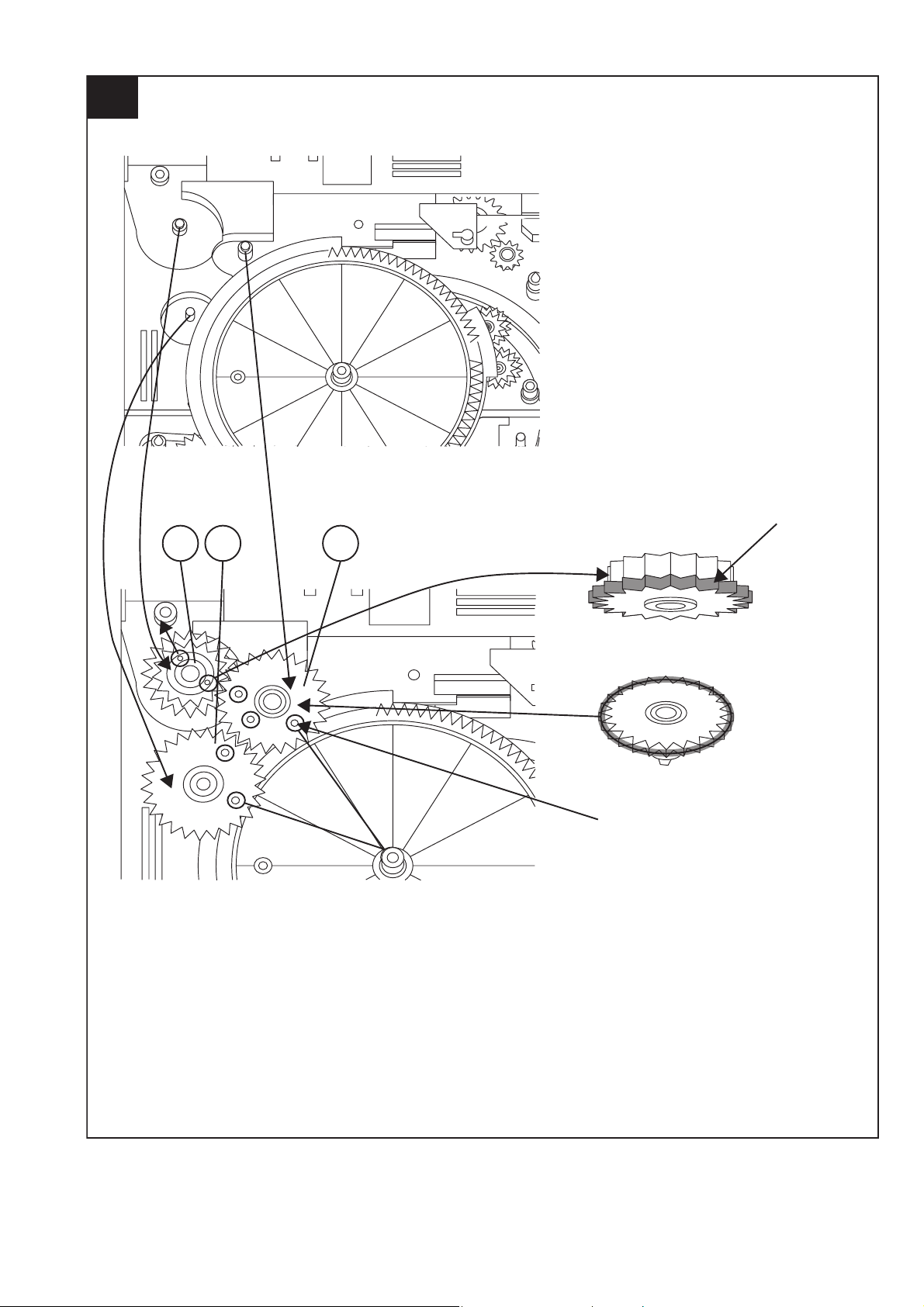
[4] CD Changer Mechanism Section
• All numbers in the drawing correspond to those in parts guide (CHANGER MECHANISM PARTS).
1
141
CD-MPX850
140
HALF GEAR
MUST BE ARRANGED AS SHOWN
2 – 5
Page 12

CD-MPX850
2
139
APPLY SANKOL SHS1001 BEFORE FIX
FIX ITEM 139 ACCORDING TO THE
PICTURE AS SHOWN ABOVE
ROTATE MODE BIG GEAR UNTIL REACH AS SHOWN IN PICTURE
2 – 6
Page 13

3
CD-MPX850
143
APPLY GREASE SC141
112
PULL THE LEVER UNITIL
REACH THE ARROW MARK
2 – 7
Page 14

CD-MPX850
4
FIGURE 2
FIGURE 1
152
142
APPLY GREASE SC141
118
SLOT CLAMP
SWITCH ARM INSIDE BASE SLOT
HALF GEAR MUST BE
ARRANGED AS SHOWN
2 – 8
Page 15

5
CD-MPX850
APPLY GREASE SC141 AT BOTTOM SIDE
OF GEAR FOLLOW MARKING (REFER TO GRAY AREA)
NO NEED TO APPLY GREASE AT BOTTOM
SIDE
FIGURE 1
APPLY GREASE SC141
AT TOP SIDE OF GEAR
FOLLOW MARKING
(REFER TO GRAY AREA)
127
IF DIRECTION IS OTHER THAN DIRECTION
SHOWN IN FIGURE 1, IT IS INCORRECT
CORRECT
128
INCORRECT
BLACK MARK
2 – 9
Page 16

CD-MPX850
6
APPLY GREASE SC141 AT
HALF GEAR AREA
ROTATE CLOCKWISE UNTIL REACH HERE (MAXIMUM)
129
2 – 10
Page 17

7
CD-MPX850
151150149
2 – 11
Page 18

CD-MPX850
8
THE SHOWN AREA MUST FREE FROM GREASE
CORRECT
GREASE SC141 APPLICATION LENGTH
GREASE APPLICATION PORTION
INCORRECT
SHOWN HOLE MUST FACING ARROW DIRECTION
124
131
2 – 12
Page 19
9
138 126 125
CD-MPX850
APPLY GREASE SC141
AT BOTTOM SIDE
ONLY
TR-RE JOINT GEAR C
APPLY GREASE SC141 ONLY AT TOP SIDE GEAR
MUST BE FIXED ACCORDINGLY TO
THE HOLE'S
2 – 13
Page 20

CD-MPX850
10
148 147 146 145
2 – 14
Page 21

11
CD-MPX850
121
144
WHEN FIXING ITEM 144 MUST FOLLOW AS SHOWN
APPLY GREASE SC141
130
2 – 15
Page 22

CD-MPX850
12
117
FIGURE 2
FIGURE 1
APPLY GREASE
SC141
FIGURE 3
APPLY GREASE SC141
2 – 16
Page 23

13
CD-MPX850
ITEM 133 , 134 MUST APPLY GREASE SC141
ON TOP SIDE GEAR ONLY
134
GEAR 112 GEAR 112
133
132
CORRECT
TOP VIEW AFTER
BEING ASSEMBLED
INCORRECT
IT IS INCORRECT TO
FIX IT IN REVERSED
DIRECTION
2 – 17
Page 24

CD-MPX850
14
APPLY GREASE SC141
BEFORE FIX
MOVE 112 UNTIL TOUCH THE WALL
B
DURING GEAR A ROTATE
MUST PRESS SHOWN AREA
A
AND LEVER B WILL MOVE
ARROW DIRECTION THEN
FIX PART 108
SCREW TORQUE
+0.5
2 kgf-cm
- 0
108 803 x6
APPLY GREASE SC141
CONFIRM WHETHER
FIXED
PROPELY OR NOT
2 – 18
Page 25

15
CD-MPX850
APPLY GREASE SC141
113
BEHIND THE LEVER NEED TO APPLY GREASE SC141
PULL IT THEN LEVER WILL
MOVE IN
2 – 19
Page 26

CD-MPX850
16
123
115
APPLY GREASE SC141
APPLY GREASE SC141 BEFORE FIX
APPLY GREASE
SC141 AT BOSS
SPRING MUST BE ARRANGED UNDER THE HOOK
CORRECT LR JOINT LEV
BOARD R
BOARD R
LR JOINT LEV
INCORRECT
2 – 20
Page 27

17
CD-MPX850
IT IS INCORRECT IF ASSEMBLED IN
A REVERSED DIRECTION
103 137 136
APPLY GREASE SC141
BIG SLOT MUST FACING OUT
WHEN FIX AND AFTER FIXED TO BASE CHASSIS.
AFTER ASSEMBLY, CONFIRM WITH FREE DROP TEST
GEAR POSITION DURING FIXING
2 – 21
Page 28

CD-MPX850
18
IT IS INCORRECT IF ASSEMBLED IN
A REVERSED DIRECTION
APPLY GREASE SC141
104
135
136
BIG SLOT MUST FACING OUT
WHEN FIX AND AFTER FIXED TO BASE CHASSIS
AFTER ASSEMBLY, CONFIRM WITH FREE DROP TEST
GEAR POSITION DURING FIXING
CONFIRM BOTH GEARS SIT PROPERLY AND LOCKED
2 – 22
Page 29

19
120
AFTER FIX OUTER UP/DOWN LEVER HOLD AS SHOWN PORTION AND
MOVE UP/DOWN THEN CONFIRM WHETHER LEVER GO INSIDE THE HOLE OR NOT
137
IT IS CORRECT IF THE LEVER HOLD
BIGGER SLOT FACING OUT
ENTERS THE HOLE
CD-MPX850
119
IT IS INCORRECT IF THE LEVER HOLD DOES NOT
ENTER THE HOLE
135
BIGGER SLOT FACING OUT
ALL OF THIS 135 AND 137 GEAR FIX TOGETHER WITH 119
AND 120 LEVER ( MOVE TOGETHER )
2 – 23
Page 30

CD-MPX850
20
BIG SLOT FACING OUT
110
2 – 24
Page 31

21
CD-MPX850
PUSH THE LEVER ACCORDING TO ARROW
DIRECTION THEN FIX
WHEN FIXING MAIN BASE ASSEMBLY FOLLOW ACCORDING TO PICTURE 1
PICTURE 1
CORRECT INCORRECT INCORRECT
MAKE SURE MECHA HOLDER SHAFT FIX PROPERLY TO LEVER
PICTURE 3
PICTURE 2
2 – 25
Page 32

CD-MPX850
22
APPLY SANKOL (SHS1001)
101
102
APPLY SANKOL
(SHS1001) ON TOP
APPLY SANKOL (SHS1001) INSIDE
THE SLOT & OTHER SHOWN PORTION
APPLY SANKOL
(SHS1001)
APPLY SANKOL (SHS1001) AT
TRAY SLIDING PORTION
FIX TRAY NO 1 FIRST THAN
FOLLOW OTHER
APPLY SANKOL (SHS1001) AT BACK PORTION
COSMO GUIDE TRAY HAVE
MARKING AS SHOWN
2 – 26
Page 33

23
GEAR UP/DOWN BOARD
111
APPLY GREASE SC141 AT INNER & OUTER GEAR SLIDING PORTION
WHEN FIX GEAR UP/
DOWN BOARD THE
TWO LEVER MUST AT
PARALLEL LINE AND
POSITIONED AT TOP
MAX SIDE
CD-MPX850
AFTER ASSEMBLY GEAR UP/DOWN BOARD
2 – 27
Page 34

CD-MPX850
24
SCREW TORQUE
+0.5
3 kgf-cm
- 0
ROTATE THE GEAR TO MOVE UP 111 GEAR
UP AND DOWN BOARD BEFORE SCREW
804
2 – 28
Page 35

25
CD-MPX850
AFTER ASSEMBLY TOP PLATE
FIX THE FFC
FFC4
AFTER PUSH, MAKE SURE SNAP PROPERLY
PRESS IN
AFTER FIX, PUSH FOLLOW ARROW DIRECTION
BEFORE LOCK
AFTER LOCK
BACK
PORTION
107
122
BEFORE LOCK
SLOT IN
BEFORE LOCK
AFTER LOCK
AFTER LOCK
MUST CONFIRM
MUST CONFIRM
2 – 29
Page 36

CD-MPX850
26
CORRECT
INCORRECT
CAUTION
1. MAKE SURE NO PWB CHIP INSIDE SET .( BEFORE FIX MAKE
SURE PWB IS FREE FROM DUST , GREASE & ETC )
803
2 – 30
Page 37

27
APPLY GREASE SC141
THE TWO SLOT MUST FREE
FROM GREASE SC141
APPLY GREASE SC141
BELOW THE MARKING
FOR BOTH PORTION
CD-MPX850
ASSEMBLY SEQUENCE
1. APPLY GREASE SC141 TO MAIN BASE
GREASE SC141 APPLICATION AREA
ALL BOSS
APPLY GREASE
SC141
CAUTION
TRAY SLIDING
AREA MUST
FREE FROM
GREASE SC141
APPLY GREASE
SC141
APPLY GREASE
APPLY GREASE SC141 AT WALL
APPLY GREASE
SC141
SC141
105
APPLY GREASE SC141
AT BOTH SLOT
APPLY GREASE SC141 AT 3 HALF MOON
1 RIB ONLY
APPLY GREASE
SC141
APPLY GREASE SC141
INSIDE SLOT
2 – 31
Page 38

CD-MPX850
28
REFERENCE ONLY
MOTOR GEAR HEIGHT FROM
MAIN BASE 12.2
+
0.1
-
0.1
-
+
12.2
MOTOR SCREWING HOLE
MUST HAVE GAP
M1,2
801
-0
13.8 + 0.2
APPLY GREASE SC141
SCREW TORQUE
1.5 + 0.5
-0
AFTER SCREW MOTOR, CONFIRM THE
ARRANGEMENT AS IN FIGURE 2
FIGURE 2
2 – 32
Page 39

29
APPLY SANKOL (SHS1001)
3.1 + 0.1
SHAFT X 3 DIM AFTER INSERTION
MUST CONFIRM EVERYDAY
SANKOL (SHS1001)
APPLICATION AREA
CD-MPX850
109-2
APPLY GREASE AT THE SLIDING PORTION
114
116
UP / DOWN
HOLDER CHANGE
TO NATURE
COLOR
APPLY GREASE SC141
2 – 33
Page 40

CD-MPX850
30
BEFORE MELT IT
AFTER MELT IT ( MUST FLAT )
WHEN FITTING STABILIZER PLATE TO STABILIZER,
ROTATE STABILIZER ANTI CLOCKWISE BY JIG
( STRICTLY CANNOT FIT USING HAND)
( BY HAND CANNOT X )
BELOW
AFTER ASSEMBLED TO
HOLDER, STABILIZER
NEED TO BE CLEANED
WITH ALCOHOL DISC
TOUCHING SURFACE
2 – 34
Page 41

31
CD-MPX850
106
APPLY GREASE SC141
MUST MAKE SURE SNAP PROPERLY BOTH SIDE
ALL SURFACE MUST TOUCH
CORRECT INCORRECT
GAP
INCORRECT
2 – 35
Page 42

CD-MPX850
32
NO GAP HAVE GAP
CORRECT INCORRECT
2 – 36
Page 43

CD-MPX850
CD-ES700/CD-ES77CD-ES700/CD-ES77Service ManualCD-ES700/CD-ES77MarketE
CHAPTER 3. MECHANISM BLOCKS
[1] Caution On Disassembly
Follow the below-mentioned notes when disassembling the unit and reassembling it, to keep it safe and ensure
excellent performance:
1. Take cassette tape and compact disc out of the unit.
2. Be sure to remove the power supply plug from the wall outlet before starting to disassemble the unit.
3. Take off nylon bands or wire holders where they need to be removed when disassembling the unit. After servicing
the unit, be sure to rearrange the leads where they were before disassembling.
STEP
1
2
3
4
5
6
7
8
9
10
11
12
13
14
REMOVAL
Top Cabinet
Side Panel (Left/
Right)
CD Changer Unit
Rear Panel with
Fan Motor
Front Panel
Main PWB
Power PWB
Tape Mechanism
Game Input PWB
Display PWB
Re-Flash PWB
CD Servo PWB
Changer
Mechanism Unit
CD Mechanism
PROCEDURE
1. Screw…………..………(A1) X 5
2. Screw……….………….(B1) X 8
1. Hook …………………...(C1) X 2
2. Socket……………….....(C2) X 1
3. Flat Cable ………..……(C3) X 1
1. Screw………….…….....(D1) X 9
1. Screw………………..…(E1) X 3
2. Flat Cable ………..……(E2) X 1
3. Socket……..….............(E3) X 1
4. Hook ……………..........(E4) X 2
1. Screw………………..…(F1) X 3
2. Socket……..…………...(F2) X 4
3. Flat Cable ………..…....(F3) X 1
1. Screw………………......(G1) X 4
1. Screw…….………….....(H1) X 6
2. Flat Cable ………..……(H2) X 1
1. Screw………………..…(J1) X 2
1. Knob……..…………..…(K1) X 1
2. Nut……………..…….....(K2) X 1
3. Washer……..….…........(K3) X 1
4. Screw……..……...........(K4) X 6
1. Screw………….............(L1) X 1
1. Screw...........................(M1) X 2
2. Flat Cable ....................(M2) X 2
3. Socket……...................(M3) X 1
1. Screw…........................(N1) X 4
2. Changer Chassis..........(N2) X 1
1. Screw…........................(P1) X 4
FIGURE
1
1
2
2
2,3
2
2
3
2,3
3
3
3
4
5
5
6
7
8
9
CD Changer
Unit
Rear Panel
(D1)x9
3x10mm
O
Figure 2
CD Servo PWB
PULL
Hook
(C1)x1
Power PWB
Fan Motor
(F2)x1
(E3)x1
(C3)x1
(F2)x2
(C2)x1
Main PWB
(F1)x1
3x10mm
O
Front Panel
(E2)x1
PULL
Lug wire
(E1)x1
3x10mm
O
Hook
(C1)x1
Note:
After removing the connector for the optical pickup from the connector,
wrap the conductive aluminium foil around the front end of the connector
so as to protect the optical pickup from electrostatic damage.
(A1)x2
3x12mm
(B1)x2
3x10mm
(A1)x1
3x12mm
Figure 1
Side Panel
(Right)
(B1)x2
3x10mm
Top Cabinet
Rear Panel
(B1)x2
3x10mm
(B1)x2
3x10mm
Front Panel
Side Panel
(Left)
(A1)x2
3x12mm
Power PWB
Figure 3
(E4)x1
PULL
(G1)x4
4x8mm
(F2)x1
(F3)x1
O
(F1)x2
3x6mm
(E1)x2
3x8mm
O
Front Panel
PULL
Hook
(E4)x1
3 – 1
Page 44

CD-MPX850
O
O
(H1)x6
O
3x10mm
Tap e
Mechanism
Figure 4
(H2)x1
Lug wire
Front Panel
(N1)x4
3x10mm
(N2)x1
Front Panel
(K4)x6
2.6x10mm
Figure 5
(J1)x2
Special
Display PWB
Nut (K2)x1
(K1)x1
Washer
(K3)x1
Game Input
PWB
(P1)x4
2.6x10mm
CD Mechanism
Figure 8
Changer
Mechanism
Unit
Changer
Mechanism
Unit
Figure 9
Figure 6
(M2)x1
Main Chasis
(M1)x2
3x10mm
(M3)x1
(L1) X 1
3X10mm
Re-Flash PWB
(M2)x1
Figure 7
CD Servo
PWB
Changer
Mechanism
Unit
3 – 2
Page 45

STEP REMOVAL PROCEDURE FIGURE
1 Woofer 1. Front Panel............(A1) x1 10
2. Socket....................(A2) x1
3. Screw.....................(A3) x2
4. Screw.....................(A4) x4
2 Tweeter 1. Screw.....................(B1) x2
3 Super tweeter
1. Screw.....................(C1) x2
CD-MPX850
Speaker Box
Front Panel
(A1)x1
(A2)x1
LED PWB
3x10mm
O
(A3)x2
3x10mm
O
WOOFER
(B1)x2
O
(C1)x2
3x10mm
(A4)x4
4x16mm
O
TWEETER
SUPER TWEETER
Screwdriver
Figure 10
3 – 3
Page 46

CD-MPX850
[2] Removing And Reinstalling The Main Parts
1. TAPE MECHANISM SECTION
Perform steps 1 to 3 and 4 of the disassembly method
to remove the tape mechanism.
1.1. How to remove the record/playback and erase
heads (TAPE 2) (See Fig. 1)
1. When you remove the screws (A1) x 2 pcs., the
recording/playback head and three-dimensional
head of the erasing head can be removed.
TAP E 2
Clutch Ass'y
Record/Playback
Head
Pinch
Pinch Roller
(C1)x1
Pull
<B>
<A>
Roller
Pawl
Figure 3
1.4. How to remove the belt (TAPE 2) (See Fig. 4)
1. Remove the main belt (D1) x 1 pc., from the motor
side.
2. Remove the FF/REW belt (D2) x 1 pc.
Erase Head
(A1)x2
2x9mm
Figure 1
1.2. How to remove the playback head (TAPE 1)(See Fig. 2)
1. When you remove the screws (B1) x 2 pcs., the
playback head can be removed.
TAP E 1
Clutch Ass'y
Playback
Head
1.5. How to remove the belt (TAPE 1) (See Fig. 4)
1. Remove the main belt (E1) x 1 pc., from the motor
side.
2. Remove the FF/REW belt (E2) x 1 pc.
Tap e
Motor
TAP E 2
Main Belt
(D1)x1
TAP E 1
Main Belt
(E1)x1
TAPE 1
FF/REW
Belt
(E2)x1
TAP E 2
FF/REW
Belt
(D2)x1
Main Belt
(D1)x1
Main Belt
(E1)x1
Tap e
Motor
Figure 4
1.6. How to remove the motor (See Fig. 5)
1. Remove the screws (F1) x 2 pcs., to remove the motor.
Tap e
Motor
(B1)x2
2x9mm
Figure 2
1.3. How to remove the pinch roller (TAPE 1/2) (See Fig. 3)
1. Carefully bend the pinch roller pawl in the direction
of the arrow <A>, and remove the pinch roller (C1) x
1 pc., in the direction of the arrow <B>.
Note:
When installing the pinch roller, pay attention to the
spring mounting position.
(F1)x2
2.6x5mm
Figure 5
3 – 4
Clutch Ass'y
Page 47

2. CHANGER MECHANISM SECTION
r
Perform steps 1, 2, 7 and 8 of the disassembly method
to remove the CD changer mechanism.
2.1 How to remove CD Disc (See Fig. 1-4)
1. When CD is at play position (Figure 1), rotate
reduction gear C clock-wise as shown in Figure 2
until disc tray is at stock position, then rotate further
to eject the disc tray so that CD can be removed
from the tray.
CD-MPX850
Reduction gear D
Up Down
Figure 3
Guide Tray
CD Disc
Disc Tray
Reduction gear C
CD Disc
CD at play position.
CD at stalk position.
Figure 1
Gear up down board
Mark 1
(DISC 1)
Figure 4
Mark 3
(DISC 3)
Mark 2
(DISC 2)
(DISC 5)
Mark 4
(DISC 4)
Mark 5
2.2 How to remove the tray motor/main cam motor/
5-Changer Motor PWB (See Fig. 5)
1. Remove the screws (A1)x 2 pcs., to remove tray
motor/main cam motor/5-Changer Motow PWB.
Changer Mechanism Unit
Front Rear
Figure 2
2. In another case, if CD mechanism is at tray No.1
play position and to remove CD located in tray No.3,
the procedure is as follows:
If the gear up down board is located at tray No.1
position, then rotate gear clock-wise until it is at
stock postiiton. Rotate reduction gear D clockwise
(Figure 3) to move the CD mechanism to tray No.3
position. This is confirmed by checking the gear up
down board position by the marking as indicated on
the main chassis as shown in Figure 4.
3 – 5
Main Cam Motor
(A1)x2
φ2x10mm
Figure 5
Tray Moto
5-Changer
Motor PWB
Note:
There are 2 more screws tighten the motors at the
bottom of main chassis. Before performing prodcedure
1 above, disc stop spring, top plate sear up down
board and trays must be removed, then only the 2
screws can be untighten.
Page 48

CD-MPX850
-MEMO-
3 – 6
Page 49

CHAPTER 4. DIAGRAMS
[1] CD Block Diagrams
CD-MPX850
XL1
16.9344 MHz
+3.3V
CONSTANT
VO LTAGE
TO MAIN SECTION
R-CH
AGND
L-CH
CE
43
CL
44
DI
45
DO
46
RESB
47
INTB0
48
INTB1
49
DVDD 1.8
38
DVDD 1.8
66
XOUT
72
XIN
73
DVDD
AVD D
36 41
+3.3V
D_+5V(+B5)
DGND
7875
LCHO
RCHO
DVDD
DVDD
+7.5V
MGND
7 1 2 3 4 5 6
CNP3
LC78690E
CD SERVO
XVDD
74
TO DISPLAY SECTION
SW3 TRAY SW2
SW2 TRAY SW1
SW1 CLAMP
SW4 DISC
MP3_INT11CD_INT12TRAY SW1/SW2
13
77
71
67
57
56
55
54
53
42
40
37
26
20
32
24
25
22
23
DISC/CLAMP
143 1 9 8 7 6 52 4
+5V
GND
PHOTO
MO_A-
CD_RES
MO_A+
CD_DI
CD_DO
CD_CLK
CD_CE
10
5251
CONT1
CONT0
IC1
PUIN
SLDO
SPDO
FDO
TDO
LDD
EIN
LDS
FIN
18 1968
1413
DIN
BIN
CIN
AIN
LRVDD
76 876521
CNP7
GND
VIN1
VIN2
17151311
VIN3
VIN4
LA6261
FOCUS/TRACKING/
PVCC1
SVCC
PVCC2
VCONT6
VCONT5
SPIN/SLIDE
DRIVER
Q1
+3.3V
LASER
DRIVER
+7.5V
9
27
28
24
21
PHOTO
5V
RX1
22
23
REV6
IC2
M1
TRAY MOTOR
M
+
--
10 113 1 9 8 7 6 52 4
32 3331 34
VO6+
FWD6
REG IN
REG OUT
4
3363521
56
M2
MAIN CAM
M
+
VO6-
VO5+
FWD5
REV5
MOTOR
CNP4
VO5-
19
20
30
7
26
8
10
Q2
+3.3V
COIL
TRACKING
PICKUP UNIT
FOCUS COIL
NM1
SPINDLE
MOTOR
NM2
SLED
MOTOR
M
M
NSW 1
PICKUP
IN
Q3
Figure 4-1: BLOCK DIAGRAM (1/3)
4 – 1
Page 50

CD-MPX850
[2] Main Block Diagrams
CHASIS_GND
11
10
9
8
7
6
5
4
3
2
1
CNP303
FM_DET
TUN_SM
R_CH
+9V
L_CH
CHASIS_GND
DO
CL
DI
CE
NC
NO USE
+B4
TUNER
PACK
UNIT
RTUNSA007AWZZ
+B7
+B7
FROM CD SECTION
TAP E 1
P.B. HEAD
TAP E 2
REC./P.B. HEAD
CNP3
L-CH
R-CH
L-CH
R-CH
ERASE
HEAD
MOTOR
DRIVER
Q709~
Q711
Q703~
Q708
SOLENOID
DRIVER
REC.
P. B .
AC BIAS
1
2
3
SWITCHING
Q101Q104
BIAS
OSC
MECHANISM
ASS'Y
BI601CNS601
1
3
4
L REC.
R REC.
SWITCHING
Q105
Q106
Q111
L103
TAPE
L(T1)
R(T1)
L(T2)
R(T2)
L NF
R NF
1
24
2
23
3
22
9
16
12
Q112
P.B
REC
T1/T2
SWITCHING
Q114
SWITCHING
JK690
VIDEO/GAME
INPUT
VIDEO/
R
JK691
VIDEO
OUT
+B4
13
4
L
P. B .
R
21
7
REC.
L
R
18
8
L NF
1 7
R NF
ALC
10
19
PLAYBACK AND RECORD/
AUX
L
VIDEO
TAP E
IN
TUNER
CD
IC101
AN7345K
PLAYBACK AMP.
Q113
SWITCHING
Q109
BIAS
Q110
+B4
9
L
16
R
10
L
15
R
L
R
L
R
LED701
LC75341
11
14
12
13
AUDIO
PROCESSOR
81817
7
Q702
+B4
23
IC601
3
Q107
Q108
MUTING
43
IXA140AW
MICROCOMPUTER
DI
CE
CLK
IC701
(2/2)
24
21
1
2
R
4
L
REC/PLAY
T1/T2
BIAS
56
Figure 4-2: BLOCK DIAGRAM (2/3)
4 – 2
Page 51

CD-MPX850
FL701
F1
F1
FL DISPLAY
---
F2
268
27 4712 54
F2
51 50
+B5
JOG701
JOG
VOLUME
REC/PLAY
T1/T2
SP. DET.
L
18
R
14
VOLTAGE REGULATOR
+B3
+B7
+B4
+B9 A_+5V
+B6
SW5V
VF2
ÐVF
VF1
+B8
D+5V
IC901
VHÐ
VLÐ
6
VL+
5
2
ÐB1
IC851
AN80T53
7
2
6
1
57 77
-
98
--
78
80
VLOAD
1415408
IC701
IXA140AW
SYSTEM
MICROCOMPUTER
99
D905
D906
D907
VH+
1
+B1
LD+8V
M+13V
A+10V
+5V
7
+B2
ÐB2
D863
+B5
11
100
8
79
VDD
Q901
Q902
Q903
Q904
R-OUT
L-OUT
3
REC/PLAY
52 53
D801
T1/T2
51
RESET
D802
D804
D803
RESET
BIAS
17 1642 18 13 10 20 23 30 31
3334
XL701
8.388 MHz
Q709
IC901
STK412-410
POWER AMP.
Q801
F802
4A/125V
F801
4A/125V
F804
2A/125V
F803
2A/125V
+B5
41
VDD
VDD
55 5
SP_RLY
CEDIDO
-
PHOTO
AVD D
CLK
T. F.
27
26
25
+B5
1
4
-
2
6
RL914
MAIN POWER
TRANSFORMER
Q713
MOTOR
DRIVER
SPEAKER
PT801
3
SW701-SW705
SW707-SW716
+B PROTECT
+B6
SECTION
+B7
Q906
Q905
RELAY
F805
4A/125V
RL841
RX701
REMOTE
1
SENSOR
2
KEY
TO CD
HEADPHONES
+B8
M
FAN MOTOR
L-CH
R-CH
SPEAKER
TERMINAL
AC POWER
SUPPLY CORD
AC 120 V, 60 Hz
+B5
JK692
M901
SO902
BIAS
IC854
+B5
3
AN78L05
CONSTANT
VOLTAGE REGULATOR
AC_RLY
1
D842 -
D845
RELAY
DRIVER
Q841
PT841
SUB POWER
TRANSFORMER
Figure 4-3: BLOCK DIAGRAM (3/3)
4 – 3
Page 52

CD-MPX850
CHAPTER 5. CIRCUIT DESCRIPTION
[1] Waveforms Of CD Circuit
1
IC1
22
FDO
1
IC1
2
IC1 IC1
1
IC1 IC1
23
22
TDO
FDO
5
6
7
IC1
3
IC1
16
TE
1
IC1
22
25
28
27
22
FDO
SPDO
PDOUT 0
PDOUT 1
FDO
3
IC1
IC1
TE
16
4
IC1
2
4
2
RFOUT
RFOUT
5 – 1
Page 53

[2] Voltage
1 1.59 21 3.24 41 3.13 61 1.55
2 0.47 22 1.62 42 0.01 62 1.93
3 0.39 23 1.63 43 0.05 63 1.93
4 2.79 24 1.62 44 2.93 64 1.93
5 1.63 25 1.64 45 2.88 65 0.00
6 1.63 26 0.00 46 1.87 66 1.81
7 1.63 27 0.33 47 3.13 67 0.00
8 1.63 28 1.62 48 3.13 68 3.13
9 1.63 29 1.10 49 3.13 69 0.03
10 1.63 30 3.05 50 0.00 70 0.02
11 1.64 31 0.00 51 3.12 71 0.01
12 0.00 32 3.26 52 3.12 72 1.34
13 1.63 33 0.03 53 0.00 73 1.53
14 1.63 34 0.03 54 0.00 74 3.01
15 1.62 35 0.03 55 0.00 75 1.54
16 1.64 36 3.26 56 0.00 76 3.23
17 1.63 37 0.02 57 0.00 77 0.00
18 3.27 38 1.81 58 0.00 78 1.59
19 0.00 39 2.56 59 1.58 79 3.24
20 0.00 40 0.00 60 1.57 80 1.59
IC 1
PIN NOVOLTAGE
(V)
PIN NOVOLTAGE
(V)
PIN NOVOLTAGE
(V)
PIN NOVOLTAGE
(V)
1 3.43 10 3.28 19 4.51 28 7.64
2 3.50 11 1.65 20 4.50 29 7.58
3 3.44 12 1.65 21 3.45 30 0.00
4 3.48 13 1.65 22 3.10 31 0.00
5 3.44 14 1.65 23 3.10 32 0.00
6 3.49 15 1.65 24 3.09 33 0.00
7 0.00 16 1.65 25 1.65 34 0.00
8 4.20 17 1.65 26 0.02 35 3.49
9 7.63 18 1.65 27 7.64 36 3.45
E 3.26 E 4.86 E 1.81 E 0.00
C 0.10 C 3.27 C 3.26 C 3.28
B 3.23 B 4.19 B 2.33 B 0.00
IC 2
Q 1
Q 2
Q 3
Q 4
VOLTAGE
(V)
PIN NOVOLTAGE
(V)
PIN NOVOLTAGE
(V)
PIN NOVOLTAGE
(V)
PIN NOVOLTAGE
(V)
PIN NOVOLTAGE
(V)
PIN NOVOLTAGE
(V)
PIN NOVOLTAGE
(V)
PIN
NO
IC701
PIN PIN
VOLTAGE
NO NO
(V) (V)
1 4.94 V
4.94 V
2 52 4.40 V
353
4.92 V
4.92 V
454
1.32 V
555
4.92 V
656
4.92 V
7 57 -29.05 V
8 0.00 V
9 4.87 V
4.87 V
10 60
4.87 V
11 61
0.00 V
12 62
0.00 V
13 63
0.00 V
14 64
0.00 V
15 65
0.00 V
16 66
0.00 V
17 67
0.00 V
18 68
0.00 V
19 69
20 70
0.00 V
0.00 V
21 71
22 4.52 V 72
23 4.41 V 73
24 4.54 V
0.00 V
25 75
0.00 V
26 76
27 1.87 V 77
4.05 V
28 78
4.07 V
29 79
0.00 V
30 80
31 4.66 V 81
32 0.23 V 82
33 4.95 V 83
34 4.95 V 84
35 85
0.00 V
0.00 V
36 86
37 13.15 V
13.15 V
38 88
13.15 V
39 89
0.00 V
40 90
41 -23.60 V 91
42 4.72 V 92
43 4.41 V
4.54 V
44 94
45 0.00 V 95
0.00 V
46 96
0.00 V
47 97
0.00 V
48 98
49 4.54 V 99
50 0.00 V 100
VOLTAGE
51
58
59
74
87
93
0.00 V
4.38 V
0.00 V
4.39 V
4.43 V
-26.42 V
-18.41 V
-29.08 V
-29.08 V
0.00 V
-29.08 V
-0.92 V
-0.96 V
-11.10 V
0.00 V
-23.60 V
-29.00 V
-23.60 V
0.00 V
0.00 V
-23.60 V
-26.20 V
-23.60 V
0.00 V
-26.40 V
0.00 V
-23.60 V
0.00 V
-23.61 V
-20.84 V
-10.43 V
-23.50 V
-26.40 V
-28.93 V
-26.40 V
-21.10 V
-25.12 V
-24.99 V
-23.01 V
-25.00 V
-24.98 V
-25.00 V
-24.85 V
-24.92 V
-24.89 V
-24.82 V
-24.87 V
-24.63 V
IC 601
PIN
VOLTAGE
NO
10
20
30
4 4.98
5 4.95
6 4.96
7 4.99
8 4.96
9 4.96
10 4.99
11 4.96
12 4.96
13 4.96
14 4.96
15 4.96
16 4.96
17 4.99
18 4.96
19 4.96
20 4.96
21 4.96
22 4.98
23 9.95
24 0
IC 901
PIN
VOLTAGE
NO
1 53.7
2 22.7
3 10.7
4 -10.7
5 -22.7
6 -53.7
70
80
90
10 0
11 0
12 -52.2
13 52.4
14 0
15 0
16 -51
17 0
18 0
5 – 2
IC101
PIN
VOLTAGE
(V)(V)(V)
NO
10
20
30
42
52
6 1.32
70
8 0.6
9 3.48
10 3.44
11 0
12 0
13 6.9
14 4.18
15 0
16 3.45
17 0.6
18 0
19 2.59
20 2
21 2
22 0
23 0
24 0
IC 503
PIN VOLTAGE
PIN
(V)
NO
1 2.55
2 2.55
3 2.55
40
5 2.49
6 2.69
7 1.34
8 12.66
IC 851
VOLTAGE
(V)
NO
1 5.06
2 12.83
3 19.6
40
5 18.28
6 9.92
7 8.4
CD-MPX850
Page 54

CD-MPX850
-MEMO-
5 – 3
Page 55

CD-MPX850
CHAPTER 6. CIRCUIT SCHEMATICS AND PARTS LAYOUT
[1] Notes On Schematic Diagram
• Resistor:
To differentiate the units of resistors, such symbol
as K and M are used: the symbol K means 1000
ohm and the symbol M means 1000 kohm and the
resistor without any symbol is ohm-type resistor.
Besides, the one with “Fusible” is a fuse type.
• Capacitor:
To indicate the unit of capacitor, a symbol P is used:
this symbol P means pico-farad and the unit of the
capacitor without such a symbol is microfarad. As to
electrolytic capacitor, the expression “capacitance/
withstand voltage” is used.
(CH), (TH), (RH), (UJ): Temperature compensation
(ML): Mylar type
(P.P.): Polypropylene type
• Schematic diagram and Wiring Side of P.W.Board
for this model are subject to change for improvement without prior notice.
• The indicated voltage in each section is the one
measured by Digital Multimeter between such a
section and the chassis with no signal given.
1. In the tuner section,
indicates AM
indicates FM stereo
2. In the main section, a tape is being played back.
3. In the deck section, a tape is being played back.
( ) indicates the record state.
4. In the power section, a tape is being played back.
5. In the CD section, the CD is stopped.
• Parts marked with “ “ ( ) are impor-
tant for maintaining the safety of the set. Be sure to
replace these parts with specified ones for maintaining the safety and performance of the set.
REF. NO DESCRIPTION POSITION
JOG701 VOLUME MAX—MIN
SW701 POWER ON /STAND-BY ON—OFF
SW702 CD ON—OFF
SW703 TUNER (BAND) ON—OFF
SW704 AUX ON—OFF
SW705 TAPE ON—OFF
SW707 PLAY ON—OFF
SW708 FAST FORWARD/PRESET UP ON—OFF
[2] Types Of Transistor And LED
FRONT
VIEW
E C B
(S)(G)(D)
(1)(2)(3)
KTA1271 Y
KTA1273 Y
KTA1274 Y
KIA78L05
KTC3199 GR
KTC3200 GR
KTC3203 Y
KTC3205 Y
B
(3)
E
(1)
KTA1504 GR
KRA107 S
KRC102 S
KRC104 S
KTA1504 Y
KTC3875 GR
REF. NO DESCRIPTION POSITION
SW709 FAST REWIND/PRESET DOWN ON—OFF
SW710 STOP ON—OFF
SW711 DISC 1 ON—OFF
SW712 DISC 2 ON—OFF
SW713 DISC 3 ON—OFF
SW714 DISC 4 ON—OFF
SW715 DISC 5 ON—OFF
SW716 OPEN/CLOSE ON—OFF
TOP VIEW
TOP
VIEW
(2)
C
MA111
1N4004
DRL204F
HSS4148
TOP VIEW
KDS184
FRONT
VIEW
AC AC
TS10B05G
6 – 1
FRONT
VIEW
503BC2E30
SLR342VC
343BD2S
Page 56

CD-MPX850
[3] Schematic Diagram
A
B
C
D
E
F
G
H
1
23456
Figure 6-1: MAIN SCHEMATIC DIAGRAM (1/6)
6 – 2
Page 57

CD-MPX850
7
8 9 10 11 12
Figure 6-2: MAIN SCHEMATIC DIAGRAM (2/6)
6 – 3
Page 58

CD-MPX850
13
14 15 16 17 18
Figure 6-3: MAIN SCHEMATIC DIAGRAM (3/6)
6 – 4
Page 59

CD-MPX850
A
B
C
D
E
F
G
H
1
23456
Figure 6-4: MAIN SCHEMATIC DIAGRAM (4/6)
6 – 5
Page 60

CD-MPX850
7
8 9 10 11 12
Figure 6-5: MAIN SCHEMATIC DIAGRAM (5/6)
6 – 6
Page 61

CD-MPX850
13
14 15 16 17 18
Figure 6-6: MAIN SCHEMATIC DIAGRAM (6/6)
6 – 7
Page 62

CD-MPX850
A
B
C
D
E
F
G
H
1
23456
Figure 6-7: POWER SCHEMATIC DIAGRAM (1/6)
6 – 8
Page 63

CD-MPX850
7
8 9 10 11 12
Figure 6-8: POWER SCHEMATIC DIAGRAM (2/6)
6 – 9
Page 64

CD-MPX850
13
14 15 16 17 18
Figure 6-9: POWER SCHEMATIC DIAGRAM (3/6)
6 – 10
Page 65

CD-MPX850
A
B
C
D
E
F
G
H
1
23456
Figure 6-10: POWER SCHEMATIC DIAGRAM (4/6)
6 – 11
Page 66

CD-MPX850
7
8 9 10 11 12
Figure 6-11: POWER SCHEMATIC DIAGRAM (5/6)
6 – 12
Page 67

CD-MPX850
13
14 15 16 17 18
Figure 6-12: POWER SCHEMATIC DIAGRAM (6/6)
6 – 13
Page 68

CD-MPX850
A
B
C
D
E
F
G
H
1
23456
Figure 6-13: DISPLAY SCHEMATIC DIAGRAM (1/6)
6 – 14
Page 69

CD-MPX850
7
8 9 10 11 12
Figure 6-14: DISPLAY SCHEMATIC DIAGRAM (2/6)
6 – 15
Page 70

CD-MPX850
13
14 15 16 17 18
Figure 6--15: DISPLAY SCHEMATIC DIAGRAM (3/6)
6 – 16
Page 71

CD-MPX850
A
B
C
D
E
F
G
H
1
23456
Figure 6-16: DISPLAY SCHEMATIC DIAGRAM (4/6)
6 – 17
Page 72

CD-MPX850
7
8 9 10 11 12
Figure 6-17: DISPLAY SCHEMATIC DIAGRAM (5/6)
6 – 18
Page 73

CD-MPX850
13
14 15 16 17 18
Figure 6-18: DISPLAY SCHEMATIC DIAGRAM (6/6)
6 – 19
Page 74

CD-MPX850
CD SIGNAL
CNS2B
CNS2A
Figure 6-19: CD MP3 SCHEMATIC DIAGRAM (1/2)
6 – 20
Page 75

CD-MPX850
Figure 6-20: CD MP3 SCHEMATIC DIAGRAM (2/2)
6 – 21
Page 76

CD-MPX850
[4] Wiring side of PWB
MAIN PWB-A1
DISPLAY PWB-B1
FFC701
20
TO
CNP701A
1
FW901
TO GAME INPUT PWB-B2
FROM TAPE 2
RECORD/PLAYBACK HEAD
FROM TAPE 1
PLAYBACK HEAD
TO
CNP3
7654321
CD MP3 PWB-C
CNS601
BL
WH
BL
WH
78910654321
CNP801
CNS801
BL
WH
BL
WH
BL
RD
FW901
TO
POWER PWB-A2
5
WTM901
1
RD
GR
BL
GR
BL
GR
BL
Q103
Q101
Q102
Q104
C137
ECB
Q111
C140
R142
15
ECB
ECB
ECB
ECB
L103
BL
WH
BL
WH
BL
WH
BL
WH
BL
RD
C132
C103
1234567
R145
C138
C139
1234567891011
CNP102
C114
R116
BI801
R111
R115
C141
D863
C851
R863
R114
C850
C134
C133
C118
C150
CNP101
C112
12 3
C111
1
C856
R929
13
24
IC855
C113
R149
2
C855
D910
C128
R113
3
D909
C126
R854
R888
R930
R928
12
IC101
R859
C117
C852
C854
R158
R866
C131
C127
C125
C143
R865
C817
ZD805
R862
R860
D862
C865
246
1357
IC851
R889
D622
R868
C862
RD
RD
RD
RD
RD
RD
RD
C918
C922
D915
12345678
R857
C859
468101214161820
2
D861
11 13 15 17 19
3579
1
BI601
C671
C861
D885
C864
C916
CNP701B
C670
R680
C915
C914
R603
R602
C621
C623
R681
R601
C609
C607
C615
C605
C613
C617
C619
C853
R853
C863
R864
C921
ZD903
R926
R925
R927
C601
IC601
C663
C662
C640
C946
213456
ZD902
R918
C603
C602
R958
R916
Lead-free solder indication
Lead-free solder is used in the MAIN PWB.
Refer to "Precautions for handling lead-free solder" for instructions
and precautions.
CNP901
Figure 6-21: WIRING SIDE OF MAIN PWB (TOP VIEW) (1/2)
6 – 22
Page 77

TUNER PACK
111
FFC303
111
246810
1357911
CNP303
C603
C610
C602
R958
C669
C664
R917R916
C606
C608
R912
IC901
C614
C616
C618
C620
C622
C624
C665
R618
C923
C902
R913
R642
R682
R622
R661
C667
C909
C906
R910
R922
01
C662
640
2 3 4 5 6 7 8 9 1011121314151617 18
R918
TO
C905
R921
C911
D905
D906
C920
CS18
CS15
CS09
D911
CS07
C641
CT21
C639
LG4
C912
CT24
QS03
RL914
E
C
B
XT21
C901
CS13
CS11
LG2
DS01
DS02
R935
QS04
DS10
RS25
RS23
ZDT21
LT2 1
LT2 2
BCE
CS10
RT22
L902
R907
R934
L901
C925
RT23
CT32
CT31
RS21
D913
R942
DS02
C926
RS22
R990
D914
R943
R941
R939
R951
Q906
Q905
R945
CS17
CS12
R959
R944
C928
CS06
CS08
3
06PN
C
12345
CNP971
BCE
BCE
D912
L921
R968
JP661
R679
21
R950
CS07
CS14
D690
D691
Q907
L920
R949
R938
C934
C936
CS05
C930
ECB
C939
C935
R940
CS16
R953
C940
C931
C937
R954
RS24
QS11
C969
R955
C942
C943
C938
C927
C929
C941
BCE
CNS01CNS02
1212
L-CHR-CH
LIGHT UP
SPEAKER
FROM SPEAKER
CNS971
BK
21
BR
L- CH
SO901
R- CH
SPEAKER TERMINAL
CD-MPX850
FROM
MAIN PWB-A1
RD
1
BK
2
WH
3
BK
45
WH
CNS603
COLOR TABLE
BR
BK
WH
RD
BL BLUE
GR GREEN
FROM
BROWN
BLACK
WHITE
RED
BI603
GAME INPUT PWB-B2
Figure 6-22: WIRING SIDE OF MAIN PWB (TOP VIEW) (2/2)
6 – 23
Page 78

CD-MPX850
0
2
6
4
MAIN PWB-A1
RS29
JP822
C693
RS27
RS01
CS01
JP819
CS03
CS19
RS03
RS30
DS03
RS05
IC503
R956
R946
R947
Q909
RS07
R984
R983
JP821
RS09
JP11
QS01
JP9
Q908
R988 R987
R937
Q903
Q904
JP816
R985
JP10
RS35
RS17
Q667
JP4
R902
R904
R606
R644
JP617
Q665
JP812
C6
R6
R6
Q
R619
R614
R685
RS11
RS19
RS15
Q668
R986
JP652
Q666
DS05
QS05
QS15
JP815
R630R631
R623
C604
JP810
R615
JP804
D601
R903
R908
C661
R683
JP665
R51
R52
R909
R905
R901
C903
C907
C908
R907
R906
C904
C913
JP823
Figure 6-23: WIRING SIDE OF MAIN PWB (BOTTOM VIEW) (1/2)
6 – 24
Q901
R920
C919
C910
R911
Page 79

CD-MPX850
R606
R644
JP617
C626
R608
R641
C612
C653
C651
C652
C625
R609
R643
JP802
JP660
C611
R607
JP601
R124 R122
C120R136
R133
R135
R138
C123
R127
R137
C119
R121
R123
JP803
Q108
C129
R131
C121
R129
JP608
R119
C115
Q107
C107
C109
R139
R130
R132
R101
C101
R117
R102
Q113
R148
C102
C135
R151
R109
R120
C116
R152
C105
Q114
R110
R146
R147
R150
R126
C124
R128
R107
C110
C108
R108
Q105
R118
C106
Q106
Q112
Q110
C104
C130
R141
R140
R103
R106
R144
R143
R104
R112
R134
R105
Q109
Q665
JP812
Q603
C917
Q604
JP807
R919
Q902
R616
R617
R620
JP809
Q885
Q886
C885
R885
R886
R887
Lead-free solder indication
Lead-free solder is used in the MAIN PWB.
Refer to "Precautions for handling lead-free solder" for instructions
and precautions.
Figure 6-24: WIRING SIDE OF MAIN PWB (BOTTOM VIEW) (2/2)
6 – 25
Page 80

CD-MPX850
POWER PWB-A2
PT841
D846
AC POWER SUPPLY
CORD (223)
AC 120V, 60Hz
3
4
2
1
C884
BL841
CNP805
BK
BK
BK
WH
WH
R890
1
234 567
T.F.
PT801
F805
4A 125V
FH809FH810
R843
R842
C843
R858
C842
D843
C841
C869
Q841
D842
ECB
D844
D845
D856
CNS702 CNS801
FH806
FH808
F803
2A 125V
FH805
C806
D804
C807
1
2
3
IC854
C805
ZD802
R802
D805
R801
2A 125V
C804
C803
D806
R805
123456
ZD801
F804
FH807
D803
R844
D853
FROM
DISPLAY PWB-B1
FH804
R806
R808
R804
CNP802
2
3456
R841
C808
FH803
F802
4A 125V
C810
C809
R891
ECB
Q801
ZD803
C801
R803
C802
1
FROM
MAIN PWB-A1
D802
CNP801
C811
891011121314151617
FH801 FH802
F801
4A 125V
COLOR TABLE
BL
D801
YL
GY
12345678910
GR
BLUE
YELLOW
GRAY
GREEN
RD RED
WH WHITE
BK BLACK
Lead-free solder indication
Lead-free solder is used in the POWER PWB.
Refer to "Precautions for handling lead-free solder"
for instructions and precautions.
Figure 6-25: WIRING SIDE OF POWER PWB
6 – 26
Page 81

-MEMO-
CD-MPX850
6 – 27
Page 82

CD-MPX850
W
W
DISPLAY PWB-B1
A
B
C
CNP701A
R743
R736
R734
CD
SW702
TAP E
SW705
R745
R742
R741
TUNER
RD03
SW703
AUX
SW704
R733
D701
R724
D703
D704
R731
R776
RX701
12 3
D713
R778
FL710
C710
R720
C702
R781
R701
R702
XL701
SW710
SW709
R706
S
RD05
S
D
LED 702
E
F
POWER
SW701
G
Lead-free solder indication
Lead-free solder is used in the DISPLAY PWB.
H
Refer to "Precautions for handling lead-free solder" for instructions
and precautions.
1
23456
Figure 6-26: WIRING SIDE OF DISPLAY PWB (TOP VIEW) (1/2)
6 – 28
Page 83

DISC 1
CD-MPX850
RD05
R706
SW707
SW708
R788
WIR_1B
R716
Q709
CNP702
26
1
3457
Q710
WIR_1A
R754
Q711
R756
DISC 5
SW715
DISC 5
D706
C712
D711
D712
SW711
OPEN/CLOSE
SW716
SW714
JOG701
R717
C719
56
R759
R766
D710
D709
DISC 3DISC 4
SW713
1234
DISC 2
SW712
C701
BI702
R763
R747
CNP703
BI701
87654 3 21
L701
C721
RD
GR
BL
GR
BL
GR
BL
7654321
1
0
7S
N
C
7654321
7654321
1UPNC
2UPNC
17
TO
TAPE MECHANISM PWB-G
7
RD
GR
YLGRYL
FFC702
GR
6
23145
LUG2
RE-FLASH PWB-E
TO
POWER PWB-B2
CNP802
COLOR TABLE
RD
RED
GR
GREEN
BL
BLUE
YL
YELLOW
8 9 10 11 12
Figure 6-27: WIRING SIDE OF DISPLAY PWB (TOP VIEW) (2/2)
6 – 29
Page 84

CD-MPX850
2
R
DISPLAY PWB-B1
A
B
RD08
RD10 RD12
RD11 RD13
C
D
R29 R27 R25 R24 R
R30 R28 R26
R766
R757
JP731
Q714
Q707
JP715
Q708
JP714
R755
R791
Q713
Q702
D707
D708
JP718
JP717
R762
R758
C705
Q705
Q706
Q704
R708
R714
R761
JP712
R760
JP724
Q703
R710
R711
R709
R713
R712
R774
R705
C704
C715
RD06
R715
RD07
R787
R703
R770
R704
R780
JP732
C708
R721
R723
R719
C707
JP702
C703
R722
R779
R775
E
JP723
R785
JP706
F
JP720
JP705
JP704
C709
R750
R784
R764
R703
C718
C706
C717
R773
R765
R771
G
JP710
H
1
23456
Figure 6-28: WIRING SIDE OF DISPLAY PWB (BOTTOM VIEW) (1/2)
6 – 30
Page 85

CD-MPX850
R25 R24 R23 R22 R21 R19 R17 R15 R13 R11 R09 R07
6
JP702
C707
C703
R718
R722
R20 R18 R16 R14 R12 R10 R08
81
80
100
1
IC701
31
30
51
50
Q712
R777
C724
R728
R727
R726
R725
R730 R732
R729
R769
C713
JP701
R06 R05 R04 R03 R02 R01
C716
RD02
RD04
R746
R752
R753
RD01
C714
R772
Lead-free solder indication
Lead-free solder is used in the DISPLAY PWB.
Refer to "Precautions for handling lead-free solder" for instructions
and precautions.
7
8 9 10 11 12
Figure 6-29: WIRING SIDE OF DISPLAY PWB (BOTTOM VIEW) (2/2)
6 – 31
Page 86

CD-MPX850
GAME INPUT PWB-B2
A
B
C
L690
1
1
2
09
3
M
TW
4
5
TO
CNP901
MAIN PWB-A1
R693
D
R691
C694
R690
E
R692
F
3
06
IB
LUG3
65
4
3
2
1
79
6C
CNS603
TO
MAIN PWB-A1
L
COLOR TABLE
WH
G
BK
RD
WHITE
BLACK
RED
Lead-free solder indication
H
1
23456
Figure 6-30: WIRING SIDE OF GAME INPUT PWB (TOP VIEW)
Lead-free solder is used in the GAME INPUT PWB.
Refer to "Precautions for handling lead-free solder" for instructions
and precautions.
6 – 32
Page 87

CD-MPX850
GAME INPUT PWB-B2
A
B
C
D
C691C690
E
F
G
Lead-free solder indication
H
Lead-free solder is used in the GAME INPUT PWB.
Refer to "Precautions for handling lead-free solder" for instructions
and precautions.
1
23456
Figure 6-31: WIRING SIDE OF GAME INPUT PWB (BOTTOM VIEW)
6 – 33
Page 88

CD-MPX850
R
C
R
R
R
R
CD MP3 PWB-C
TO
PICK-UP UNIT
FROM
MAIN PWB-A1
BI601
WIRE_A
C27
C22
C36
R17
C41
C44
C43
C46
C8
C42
C6
C29
R7
C35
C20
R2
C7
R54
R5
R3
XL1
C4
R53
R6
R66
CNP1
C5
R1
R4
C25
13579111315
246810121416
C1
R13
R23
R24
R35
R40
R41
R42
C11
R29
CNP7
C3
R10
R25
R12
R9
R27 R11
WIRE_A’
IC2
Q2
R62
R57
CNS601
BLBRBLGRBL
GR
RD
1234567
CNP3
Figure 6-32: WIRING SIDE OF CD MP3 PWB (TOP VIEW) (1/2)
6 – 34
Page 89

CD-MPX850
IC2
Q2
R62
R57
C58
R20
R19
R21
R22
R26
C57
C10
J29
CNP2
CNP4
123456
RD
123456
WH
123456
GR
WH
GR
WH
TO
CD MOTOR PWB
Lead-free solder indication
Lead-free solder is used in the CD MP3, CD CHANGER MOTOR PWB.
Refer to "Precautions for handling lead-free solder" for instructions
and precautions.
Figure 6-33: WIRING SIDE OF CD MP3 PWB (TOP VIEW) (2/2)
6 – 35
COLOR TABLE
GR
RD
BR
BL
GREEN
RED
BROWN
BLUE
WH WHITE
Page 90

CD-MPX850
CD MP3 PWB-C
R8
JP10
R28
JP9
R61
R60
R59
R58
JP1
IC2
JP12
JP21
JP11
R63
C21
R33
R34
C9
C51
R64
C53
C54
C23
C24
JP2
C31
R32
C50
C52
R36
R55
JP3
R37
C26
TP5
JP17
JP14
R38
R15
R14
JP7
JP8
C55
C56
R39
Q4
C2
JP15
R44
C33
R43
JP6
R68
R67
C37
R65
JP20
JP16
D1
C18
TP4
JP18
IC1
TP3
R46
C34
R45
C32
JP19
C28
C17
C16
C15
C59
TP1
FB2
TP2
R47
JP13
C49
Q1
C47
R16
R48
C13
C12
R31
C14
C48
R30
C30
C19
C40
FB1
Q3
R18
R52
C45
R49
R50R51
Lead-free solder indication
Lead-free solder is used in the CD MP3 PWB.
Refer to "Precautions for handling lead-free solder" for instructions
and precautions.
Figure 6-34: WIRING SIDE OF CD MP3 PWB (BOTTOM VIEW)
6 – 36
Page 91

TAPE MECHANISM PWB-G
TO
DISPLAY PWB-B1
CNP702
CD-MPX850
SOLENOID
COLOR TABLE
RD
WH
BK
YL
RED
WHITE
BLACK
YELLOW
GR GREEN
TAPE MOTOR
TAP E 1
PLAYBACK
HEAD
CNP101
TO
MAIN PWB-A1
SOLENOID
ERASE
HEAD
MAIN PWB-A1
TAPE 2
CNP102
TO
RECORD/
PLAYBACK
HEAD
Figure 6-35: WIRING SIDE OF TAPE MECHANISM PWB
6 – 37
Page 92

PARTS GUIDE
MINI COMPONENT SYSTEM
CD-MPX850
[1] INTEGRATED CIRCUITS
[2] TRANSISTORS
[3] DIODES
[4] VIBRATORS / CRYSTALS
[5] TRANSFOMERS
MODEL
CD-MPX850 Mini Component System consisting of
CD-MPX850
system).
CONTENTS
[9] OTHER CIRCUITRY PARTS
[10] CHANGER MECHANISM /
[11] CABINET PARTS
[12] SPEAKER BOX PARTS
CD-MPX850
(main unit) and CP-MPX850 (speaker
CD MECHANISM PARTS
[13] ACCESSORIES / PACKING
[6] COILS
[7] CAPACITORS
[14] P.W.B. ASSEMBLY
PARTS
(Not Replacement Item)
[8] RESISTORS
[15] OTHER SERVICE PARTS
Parts marked with " " are important for maintaining the safety of the set. Be sure to replace these parts with
specified ones for maintaining the safety and performance of the set.
!
SHARP CORPORATION
0
This document has been published to be used
for after sales service only.
The contents are subject to change without notice.
Page 93

CD-MPX850
NO. PARTS CODE
[1] INTEGRATED CIRCUITS
IC1 VHILC78690E-1 BE CD Servo,LC78690
IC2 VHILA6261//-1 AN Focus/Tracking/Spin/Sled Driver, LA6261
IC101 VHIAN7345K/-1 AM Playback and Record / Playback Amp.,AN7345K
IC503 VHIAZ4558CME1 AD Op Amp Z4558CME
IC601 VHILC75341/-1 AM Audio Processor,LC75341
IC701 RH-IXA140AW00 BM System Microcomputer, IXA140AW
IC851 VHIAN80T53/-1 AL Multi Regulator,AN80T53
IC854 VHIKIA78L05-1 AE Constant Voltage Regulator,KIA78L05
IC901 VHISTK41241-1 BA Power Amplifier, STK412410
[2] TRANSISTORS
Q1 VSKTA1504Y/-1 AB Silicon,PNP,KTA1504 Y
Q2 VSKTA1271Y/-1 AC Silicon,PNP,KTA1271 Y
Q3 VSKTC3875GR-1 AB Silicon,NPN,KTC3875 GR
Q4 VSKRC104S//-1 AC Digital,NPN,KRC104 S
Q101 VSKTC3200GR-1 AB Silicon,NPN,KTC3200 GR
Q102 VSKTC3200GR-1 AB Silicon,NPN,KTC3200 GR
Q103 VSKTC3200GR-1 AB Silicon,NPN,KTC3200 GR
Q104 VSKTC3200GR-1 AB Silicon,NPN,KTC3200 GR
Q105 VSKTC3875GR-1 AB Silicon,NPN,KTC3875 GR
Q106 VSKTC3875GR-1 AB Silicon,NPN,KTC3875 GR
Q107 VSKTC3875GR-1 AB Silicon,NPN,KTC3875 GR
Q108 VSKTC3875GR-1 AB Silicon,NPN,KTC3875 GR
Q109 VSKTA1504Y/-1 AB Silicon,PNP,KTA1504 Y
Q110 VSKRC104S//-1 AC Digital,NPN,KRC104 S
Q111 VSKTC3203Y/-1 AE Silicon,NPN,KTC3203 Y
Q112 VSKTA1504Y/-1 AB Silicon,PNP,KTA1504 Y
Q113 VSKRC104S//-1 AC Digital,NPN,KRC104 S
Q114 VSKRC104S//-1 AC Digital,NPN,KRC104 S
Q603 VSKTC3875GR-1 AB Silicon,NPN,KTC3875 GR
Q604 VSKTC3875GR-1 AB Silicon,NPN,KTC3875 GR
Q665 VSKRA107S//-1 AB Digital,PNP,KRA107 S
Q666 VSKTC3875GR-1 AB Silicon,NPN,KTC3875 GR
Q667 VSKTA1504GR-1 AB Silicon,PNP,KTA1504 GR
Q668 VSKTC3875GR-1 AB Silicon,NPN,KTC3875 GR
Q702 VSKRC102S//-1 AB Digital,NPN,KRC102 S
Q703 VSKRA107S//-1 AB Digital,PNP,KRA107 S
Q704 VSKRC104S//-1 AC Digital,NPN,KRC104 S
Q705 VSKRA107S//-1 AB Digital,PNP,KRA107 S
Q706 VSKRC104S//-1 AC Digital,NPN,KRC104 S
Q707 VSKRA107S//-1 AB Digital,PNP,KRA107 S
Q708 VSKRC104S//-1 AC Digital,NPN,KRC104 S
Q709 VSKTA1273Y/-1 AE Silicon,PNP,KTA1273 Y
Q710 VSKTA1273Y/-1 AE Silicon,PNP,KTA1273 Y
Q711 VSKTA1273Y/-1 AE Silicon,PNP,KTA1273 Y
Q712 VSKRC102S//-1 AB Digital,NPN,KRC102 S
Q713 VSKRC104S//-1 AC Digital,NPN,KRC104 S
Q801 VSKTA1274Y/-1 AE Silicon,PNP,KTA1274 Y
Q841 VSKTC3199GR-1 AB Silicon,NPN,KTC3199 GR
Q885 VSKTC3875GR-1 AB Silicon,NPN,KTC3875 GR
Q886 VSKTC3875GR-1 AB Silicon,NPN,KTC3875 GR
Q901 VSKTC3875GR-1 AB Silicon,NPN,KTC3875 GR
Q902 VSKTC3875GR-1 AB Silicon,NPN,KTC3875 GR
Q903 VSKTC3875GR-1 AB Silicon,NPN,KTC3875 GR
Q904 VSKTC3875GR-1 AB Silicon,NPN,KTC3875 GR
Q905 VSKTC3199GR-1 AB Silicon,NPN,KTC3199 GR
Q906 VSKTC3203Y/-1 AE Silicon,NPN,KTC3203 Y
Q908 VSKTC3875GR-1 AB Silicon,NPN,KTC3875 GR
Q909 VSKTC3875GR-1 AB Silicon,NPN,KTC3875 GR
QS01 VSKTC3875GR-1 AB Silicon,NPN,KTC3875 GR
QS03 VSKTC3205Y/-1 AD Silicon,NPN,KTC3205 Y
QS05 VSKRC104S//-1 AC Digital,NPN,KRC104 S
QS11 VSKTC3199GR-1 AB Silicon,NPN,KTC3199 GR
QS15 VSKRC104S//-1 AC Digital,NPN,KRC104 S
[3] DIODES
D1 VHDKDS184//-1 AB Silicon,KDS184
D601 VHDMA111///-1 AC Silicon,MA111
D622 VHDGD1A4+++-1 AB Silicon, GD1A4
D690 VHDHSS4148+-1 AA Silicon,DHSS4148
D691 VHDHSS4148+-1 AA Silicon,DHSS4148
D702 VHDHSS4148+-1 AA Silicon,DHSS4148
D703 VHDHSS4148+-1 AA Silicon,DHSS4148
D704 VHDHSS4148+-1 AA Silicon,DHSS4148
D706 VHDHSS4148+-1 AA Silicon,DHSS4148
D707 VHDMA111///-1 AC Silicon,MA111
D708 VHDMA111///-1 AC Silicon,MA111
D709 VHDHSS4148+-1 AA Silicon,DHSS4148
D710 VHDHSS4148+-1 AA Silicon,DHSS4148
D711 VHDHSS4148+-1 AA Silicon,DHSS4148
D712 VHDHSS4148+-1 AA Silicon,DHSS4148
D713 VHDHSS4148+-1 AA Silicon,DHSS4148
D752 VHD1N4148H/-1 AA Silicon,1N4148H (Use in LED PWB-D) Use 2 pcs
D801 VHDTS10B05G-1 AH Silicon,TS10B05GM
D802 VHDTS10B05G-1 AH Silicon,TS10B05GM
D803 VHDRL204F//-1 AC Silicon,DRL204F
D804 VHDRL204F//-1 AC Silicon,DRL204F
D805 VHD1N4004S/-1 AB Silicon,IN4004S
PRICE
RANK
NEW
MARK
PAR T
RANK
DESCRIPTION
1
Page 94

NO. PARTS CODE
PRICE
RANK
NEW
MARK
PAR T
RANK
[3] DIODES
D806 VHD1N4004S/-1 AB Silicon,IN4004S
D842 VHD1N4004S/-1 AB Silicon,IN4004S
D843 VHD1N4004S/-1 AB Silicon,IN4004S
D844 VHD1N4004S/-1 AB Silicon,IN4004S
D845 VHD1N4004S/-1 AB Silicon,IN4004S
D846 VHD1N4004S/-1 AB Silicon,IN4004S
D853 VHD1N4004S/-1 AB Silicon,IN4004S
D856 VHDHSS4148+-1 AA Silicon,DHSS4148
D860 VHDHSS4148+-1 AA Silicon,DHSS4148
D861 VHDHSS4148+-1 AA Silicon,DHSS4148
D862 VHDHSS4148+-1 AA Silicon,DHSS4148
D863 VHDHSS4148+-1 AA Silicon,DHSS4148
D885 VHDHSS4148+-1 AA Silicon,DHSS4148
D905 VHDHSS4148+-1 AA Silicon,DHSS4148
D906 VHDHSS4148+-1 AA Silicon,DHSS4148
D907 VHDHSS4148+-1 AA Silicon,DHSS4148
D909 VHD1N4004S/-1 AB Silicon,IN4004S
D910 VHDDS1N404S-1 AB Silicon,DS1N404S
D911 VHDHSS4148+-1 AA Silicon,DHSS4148
D912 VHDHSS4148+-1 AA Silicon,DHSS4148
D913 VHDHSS4148+-1 AA Silicon,DHSS4148
D914 VHDHSS4148+-1 AA Silicon,DHSS4148
DS01 VHDHSS4148+-1 AA Silicon,DHSS4148
DS03 VHDMA111///-1 AC Silicon,MA111
DS05 VHDMA111///-1 AC Silicon,MA111
DS09 VHDHSS4148+-1 AA Silicon,DHSS4148
LED701 VHP503BC2E30Z AG LED,Blue,5mm,503BC2E30
LED702 VHPA343BD2S2Z AG LED,Blue A343BD2S2Z ( LED PWB-D ) use 2 pcs
LED702 VHPSLR342VCB1 AC LED,Red,SLR342VCB ( DISPLAY PWB-B1 )
ZD801 RH-EX0617GEZZY AB Zener,6.2V
ZD802 RH-EX0624GEZZY AB Zener,7.5V
ZD803 RH-EX0671GEZZY AB Zener,30V
ZD805 RH-EX0640GEZZY AB Zener,12V
ZD902 RH-EX0640GEZZY AB Zener,12V
ZD903 RH-EX0640GEZZY AB Zener,12V
[4] VIBRATORS/CRYSTALS
XL1 RCRM-0047AWZZ AE Ceramic
XL701 RCRSP0029AWZZ AF Crystal
[5] TRANSFORMERS
PT801 RTRNPA015AWZZ BE Power ( Main )
PT841 RTRNP0483AWZZ AL Power ( Sub )
[6] COILS
FB1 RBLN-0061TAZZ AB Ferrite Beads,BLM18AG121SN1D
FB2 RBLN-0061TAZZ AB Ferrite Beads,BLM18AG121SN1D
L103 VP-MK331K0000 AB 330 µ H,Choke
L701 VP-DH101K0000 AB 100 µ H,Choke
L901 RCILZ0024AWZZ AC 3 µ H,Choke
L902 RCILZ0024AWZZ AC 3 µ H,Choke
L920 RCILZA017AWZZ AB 0.29 µ H
L921 RCILZA017AWZZ AB 0.29 µ H
[7] CAPACITORS
C1 VCEAZA1AW107M AB 100µF,10V,Electrolytic
C2 VCKYCY1HB102K AA 0.001µF,50V
C3 VCEAZA1AW107M AB 100µF,10V,Electrolytic
C4 VCKYPA1HB103K AA 0.01µF,50V
C5 VCEAZA1EW476M AB 47µF,25V,Electrolytic
C6 RC-EZ0004AWZZ AD 3.3µF,16V,Electrolytic
C7 VCKYPA1HB102K AA 0.001µF,50V
C8 VCEAZA1AW476M AB 47µF,10V,Electrolytic
C9 VCKYCY1HB103K AA 0.01µF,50V
C10 VCEAZA0JW108M AC 1000µF,6.3V,Electrolytic
C11 VCEAZA1AW107M AB 100µF,10V,Electrolytic
C12 VCKYCY1HB472K AA 0.0047µF,50V
C13 VCKYCY1HB103K AA 0.01µF,50V
C14 VCKYCY1EF473Z AB 0.047µF,25V
C15 VCKYCY1CB563K AA 0.056µF,16V
C16 VCKYCY1HB103K AA 0.01µF,50V
C17 VCKYCY1CB563K AA 0.056µF,16V
C18 VCKYCY1HB103K AA 0.01µF,50V
C19 VCKYCY1CB104K AA 0.1µF,16V
C20 VCEAZA1AW107M AB 100 µ F,10V,Electrolytic
C21 VCKYCY1CB104K AA 0.1µF,16V
C22 VCEAZA1AW477M AB 470µF,10V,Electrolytic
C23 VCKYCY1CB104K AA 0.1µF,16V
C24 VCKYCY1CB104K AA 0.1µF,16V
C25 VCEAZA1HW224M AB 0.22µF,50V,Electrolytic
C26 VCKYCY1EF473Z AB 0.047µF,25V
C27 VCEAZA1AW107M AB 100µF,10V,Electrolytic
C28 VCKYCY1CB104K AA 0.1µF,16V
C29 VCEAZA1AW107M AB 100µF,10V,Electrolytic
C30 VCKYCY1CB104K AA 0.1µF,16V
C31 VCKYCY1CB104K AA 0.1µF,16V
C32 VCKYCY1CB104K AA 0.1µF,16V
CD-MPX850
DESCRIPTION
2
Page 95

CD-MPX850
NO. PARTS CODE
[7] CAPACITORS
C33 VCKYCY1CB104K AA 0.1µF,16V
C34 VCKYCY1CB104K AA 0.1µF,16V
C35 VCEAZA1HW105M AB 1µF,50V,Electrolytic
C36 VCEAZA1AW107M AB 100µF,10V,Electrolytic
C37 VCKYCY1CB104K AA 0.1 µ F,16V
C40 VCKYCY1CB104K AA 0.1µF,16V
C41 VCEAZA1HW106M AB 10µF,50V,Electrolytic
C42 VCEAZA1HW106M AB 10µF,50V,Electrolytic
C43 VCKYPA1HB152K AA 0.0015µF,50V
C44 VCKYPA1HB152K AA 0.0015µF,50V
C45 VCKYCY1CB104K AA 0.1µF,16V
C46 VCEAZA1AW477M AB 470µF,10V,Electrolytic
C47 VCKYCY1EF473Z AB 0.047µF,25V
C48 VCKYCY1HB103K AA 0.01µF,50V
C49 VCKYCY1EF223Z AB 0.022µF,25V
C50 VCCCCY1HH101J AA 100p F (CH), 50V
C51 VCCCCY1HH101J AA 100p F (CH), 50V
C52 VCCCCY1HH101J AA 100p F (CH), 50V
C53 VCCCCY1HH101J AA 100p F (CH), 50V
C54 VCKYCY1EF223Z AB 0.022µF,25V
C55 VCCCCY1HH101J AA 100p F (CH), 50V
C56 VCCCCY1HH101J AA 100p F (CH), 50V
C57 VCEAZA1AW107M AB 100µF,10V,Electrolytic
C58 VCKYBT1HB103K AA 0.01µF,50V
C59 VCKYCY1HB822K AA 0.0082µF,50V
C101 VCKYCY1HB561K AA 560 p F,50V
C102 VCKYCY1HB561K AA 560 p F,50V
C103 VCKYBT1HB181K AA 180 p F,50V
C104 VCCCCY1HH181J AA 180 p F (CH),50V
C105 VCKYCY1HB561K AA 560 p F,50V
C106 VCKYCY1HB561K AA 560 p F,50V
C107 VCKYCY1HB331K AA 330 p F,50V
C108 VCKYCY1HB331K AA 330 p F,50V
C109 VCKYCY1HB331K AA 330 p F,50V
C110 VCKYCY1HB331K AA 330 p F,50V
C111 VCEAZA1EW476M AB 47 µ F,25V,Electrolytic
C112 VCEAZA1EW476M AB 47 µ F,25V,Electrolytic
C113 VCQYKA1HM393K AB 0.039µF,50V,Mylar
C114 VCQYKA1HM393K AB 0.039µF,50V,Mylar
C115 VCKYCY1HB561K AA 560 p F,50V
C116 VCKYCY1HB561K AA 560 p F,50V
C117 VCEAZA1EW476M AB 47 µ F,25V,Electrolytic
C118 VCEAZA1EW476M AB 47 µ F,25V,Electrolytic
C119 VCKYCY1HB222K AA 0.0022 µ F,50V
C120 VCKYCY1HB222K AA 0.0022 µ F,50V
C121 VCKYCY1EF223Z AB 0.022 µ F,25V
C123 VCKYCY1HB271K AA 270 p F,50V
C124 VCKYCY1HB271K AA 270 p F,50V
C125 VCEAZA1EW226M AB 22 µ F,25V,Electrolytic
C126 VCEAZA1EW226M AB 22 µ F,25V,Electrolytic
C127 VCQYKA1HM223K AB 0.022µF,50V,Mylar
C128 VCQYKA1HM223K AB 0.022µF,50V,Mylar
C129 VCKYCY1HB332K AA 0.0033 µ F,50V
C130 VCKYCY1HB332K AA 0.0033 µ F,50V
C131 VCEAZA1EW476M AB 47 µ F,25V,Electrolytic
C132 VCEAZA1EW476M AB 47 µ F,25V,Electrolytic
C133 VCEAZA1EW226M AB 22 µ F,25V,Electrolytic
C134 VCEAZA1AW227M AC 220 µ F,10V,Electrolytic
C135 VCKYCY1EF223Z AB 0.022 µ F,25V
C137 VCQYKA1HM473K AB 0.047 µ F,50V,Mylar
C138 VCQPKAA2AA822J AA 0.0082 µ F,50V,Thin Film
C139 VCQYKA1HM393K AB 0.039 µ F,50V,Thin Film
C140 VCEAZA1EW476M AB 47 µ F,25V,Electrolytic
C141 VCEAZA1CW107M AC 100 µ F,16V,Electrolytic
C143 VCEAZA1HW335M AB 3.3 µ F,50V,Electrolytic
C150 VCEAZA1EW476M AB 47 µ F,25V,Electrolytic
C601 VCEAZA1CW227M AC 220 µ F,16V,Electrolytic
C602 VCQYKA1HM223K AB 0.022µF,50V,Mylar
C603 VCEAZA1AW227M AC 220 µ F,10V,Electrolytic
C604 VCKYCY1HB681K AA 680 p F,50V
C605 VCEAZA1HW475M AB 4.7 µ F,50V,Electrolytic
C606 VCQYKA1HM823K AC 0.082µF,50V,Mylar
C607 VCQYKA1HM823K AC 0.082µF,50V,Mylar
C608 VCFYFA1HA124J AB 0.12µF,50V,Thin Film
C609 VCEAZA1HW105M AB 1 µ F,50V,Electrolytic
C610 VCEAZA1HW105M AB 1 µ F,50V,Electrolytic
C611 VCKYCY1HB272K AA 0.0027 µ F,50V
C612 VCKYCY1HB272K AA 0.0027 µ F,50V
C613 VCEAZA1HW105M AB 1 µ F,50V,Electrolytic
C614 VCEAZA1HW105M AB 1 µ F,50V,Electrolytic
C615 VCFYFA1HA124J AB 0.12µF,50V,Thin Film
C616 VCEAZA1HW475M AB 4.7 µ F,50V,Electrolytic
C617 VCEAZA1HW105M AB 1 µ F,50V,Electrolytic
C618 VCEAZA1HW105M AB 1 µ F,50V,Electrolytic
C619 VCEAZA1HW105M AB 1 µ F,50V,Electrolytic
C620 VCEAZA1HW105M AB 1 µ F,50V,Electrolytic
C621 VCEAZA1HW105M AB 1 µ F,50V,Electrolytic
C622 VCEAZA1HW105M AB 1 µ F,50V,Electrolytic
PRICE
RANK
NEW
MARK
PAR T
RANK
DESCRIPTION
3
Page 96

NO. PARTS CODE
[7] CAPACITORS
C623 VCEAZA1HW105M AB 1 µ F,50V,Electrolytic
C624 VCEAZA1HW105M AB 1 µ F,50V,Electrolytic
C625 VCKYCY1HB222K AA 0.0022 µ F,50V
C626 VCKYCY1HB222K AA 0.0022 µ F,50V
C640 VCEAZA1HW226M AB 22 µ F,50V,Electrolytic
C641 VCEAZA1AW107M AB 100 µ F,10V,Electrolytic
C651 VCKYCY1HB221K AA 220 p F,50V
C652 VCKYCY1HB221K AA 220 p F,50V
C653 VCKYCY1HB221K AA 220 p F,50V
C661 VCKYCY1HB681K AA 680 p F,50V
C690 VCKYCY1HB391K AA 390 p F,50V
C691 VCKYCY1HB391K AA 390 p F,50V
C693 VCKYCY1EF104Z AA 0.1µF,25V
C694 VCQYKA1HM103K AA 0.01µF,50V,Mylar
C697 VCQYKA1HM102K AA 0.001µF,50V,Mylar
C701 VCEAZA1HW105M AB 1 µ F,50V,Electrolytic
C702 VCEAZA1AW227M AC 220 µ F,10V,Electrolytic
C703 VCKYCY1EF223Z AB 0.022 µ F,25V
C704 VCKYCY1EF223Z AB 0.022 µ F,25V
C705 VCKYCY1EF473Z AB 0.047 µ F,25V
C706 VCKYCY1EF473Z AB 0.047 µ F,25V
C707 VCCCCY1HH150J AA 15 p F (CH),50V
C708 VCCCCY1HH150J AA 15 p F (CH),50V
C709 VCKYCY1EF223Z AB 0.022 µ F,25V
C710 VCEAZA1EW476M AB 47 µ F,25V,Electrolytic
C712 VCEAZA1HW335M AB 3.3 µ F,50V,Electrolytic
C713 VCKYCY1HB103K AA 0.01 µ F,50V
C714 VCKYCY1EF473Z AB 0.047µF,25V
C715 VCKYCY1HB103K AA 0.01 µ F,50V
C716 VCKYCY1EF223Z AB 0.022 µ F,25V
C717 VCKYCY1HB473K AA 0.047 µ F,50V
C718 VCKYCY1HB473K AA 0.047 µ F,50V
C721 VCEAZA1HW105M AB 1 µ F,50V,Electrolytic
C724 VCCCCY1HH151J AA 150 p F (CH),50V
C801 VCEAZA1VW107M AC 100 µ F,35V,Electrolytic
C802 VCEAZA1HW476M AB 47 µ F,50V,Electrolytic
C803 VCEAZA1HW476M AB 47 µ F,50V,Electrolytic
C804 VCEAZA1JW227M AB 220 µ F,63V,Electrolytic
C805 VCEAZA2AW226M AC 22 µ F,100V,Electrolytic
C806 VCFYFA1HA104J AB 0.1 µ F,50V,Thin Film
C807 VCFYFA1HA104J AB 0.1 µ F,50V,Thin Film
C808 VCFYFA1HA104J AB 0.1µF,50V,Thin Film
C809 VCFYFA1HA104J AB 0.1µF,50V,Thin Film
C810 VCFYDA2AA224J AD 0.22 µ F,50V,Thin Film
C811 VCFYDA2AA224J AD 0.22 µ F,50V,Thin Film
C841 VCEAZA0JW108M AC 1000µF,6.3V,Electrolytic
C842 VCEAZA1VW477M AD 470µF,35V,Electrolytic
C843 VCQYKA1HM473K AB 0.047µF,50V,Mylar
!
C844 RC-KZ002LAWZZ AC 4700pF,250V,Ceramic
C850 VCEAZW1EW478M AK 4700 µ F,25V,Electrolytic
C854 VCEAZA1EW227M AC 220 µ F,25V,Electrolytic
C855 VCEAZA1HW476M AB 47 µ F,50V,Electrolytic
C856 VCFYFA1HA104J AB 0.1µF,50V,Thin Film
C859 VCEAZA1HW226M AB 22µF,50V,Electrolytic
C861 VCQYKA1HM223K AB 0.022µF,50V,Mylar
C864 VCEAZA1EW226M AB 22 µ F,25V,Electrolytic
C865 VCEAZA1EW226M AB 22 µ F,25V,Electrolytic
C869 VCQYKA1HM223K AB 0.022µF,50V,Mylar
C885 VCKYCY1HB104K AA 0.1µF,50V
C901 VCEAZA1HW105M AB 1 µ F,50V,Electrolytic
C902 VCEAZA1HW105M AB 1 µ F,50V,Electrolytic
C903 VCKYCY1HB102K AA 0.001 µ F,50V
C904 VCKYCY1HB102K AA 0.001 µ F,50V
C905 VCEAZA1HW335M AB 3.3µF,50V,Electrolytic
C906 VCEAZA1HW335M AB 3.3µF,50V,Electrolytic
C907 VCCCCY1HH101J AA 100 p F (CH),50V
C908 VCCCCY1HH3R0C AA 3 p F (CH),50V
C909 VCFYFA1HA104J AB 0.1µF,50V,Thin Film
C910 VCCCCY1HH3R0C AA 3 p F (CH),50V
C911 VCEAZA2AW107M AD 100 µ F,100V,Electrolytic
C912 VCEAZA2AW107M AD 100 µ F,100V,Electrolytic
C913 VCCCCY1HH101J AA 100 p F (CH),50V
C914 VCEAZA2AW107M AD 100 µ F,100V,Electrolytic
C915 VCEAZA2AW107M AD 100 µ F,100V,Electrolytic
C916 VCEAZA1HW107M AC 100 µ F,50V,Electrolytic
C917 VCKYCY1HB103K AA 0.01 µ F,50V
C918 VCEAZA1HW107M AC 100 µ F,50V,Electrolytic
C919 VCKYCY1HB103K AA 0.01 µ F,50V
C920 RC-EZ0029AWZZ AN 3300 µ F,71V,Electrolytic
C921 RC-EZ3016AWZZ AG 4700 µ F,35V,Electrolytic
C922 RC-EZ3016AWZZ AG 4700 µ F,35V,Electrolytic
C923 RC-EZ0029AWZZ AN 3300 µ F,71V,Electrolytic
C925 VCEAZA1HW476M AB 47 µ F,50V,Electrolytic
C928 VCFYFA1HA104J AB 0.1µF,50V,Thin Film
C929 VCFYFA1HA104J AB 0.1µF,50V,Thin Film
C939 VCEAZA1HW106M AB 10 µ F,50V,Electrolytic
C946 VCEAZA1HW104M AB 0.1 µ F,50V,Electrolytic
CS01 VCKYCY1HB102K AA 0.001 µ F,50V
PRICE
RANK
NEW
MARK
PAR T
RANK
CD-MPX850
DESCRIPTION
4
Page 97

CD-MPX850
NO. PARTS CODE
PRICE
RANK
[7] CAPACITORS
CS03 VCCCCY1HH101J AA 100 p F (CH),50V
CS07 VCEAZA1HW226M AB 22 µ F,50V,Electrolytic
CS09 VCEAZA1HW226M AB 22 µ F,50V,Electrolytic
CS13 VCEAZA1HW106M AB 10 µ F,50V,Electrolytic
CS15 VCEAZA1EW476M AB 47 µ F,25V,Electrolytic
CS18 VCEAZA1CW106M AC 10 µ F,16V,Electrolytic
CS19 VCKYCY1HB104K AA 0.1µF,50V
[8] RESISTORS
JP1 VRS-CY1JB000J AA 0 ohms,Jumper,0.8x1.55mm,Green
JP2 VRS-CY1JB000J AA 0 ohms,Jumper,0.8x1.55mm,Green
JP3 VRS-CY1JB000J AA 0 ohms,Jumper,0.8x1.55mm,Green
JP4 VRS-CY1JB000J AA 0 ohms,Jumper,0.8x1.55mm,Green
JP6 VRS-CY1JB000J AA 0 ohms,Jumper,0.8x1.55mm,Green
JP7 VRS-CY1JB000J AA 0 ohms,Jumper,0.8x1.55mm,Green
JP8 VRS-CY1JB000J AA 0 ohms,Jumper,0.8x1.55mm,Green
JP9 VRS-CY1JB000J AA 0 ohms,Jumper,0.8x1.55mm,Green (MAIN PWB-A1)
JP10 VRS-CY1JB000J AA 0 ohms,Jumper,0.8x1.55mm,Green (CD MP3 PWB-C)
JP11 VRS-CY1JB000J AA 0 ohms,Jumper,0.8x1.55mm,Green (CD MP3 PWB-C)
JP12 VRS-CY1JB000J AA 0 ohms,Jumper,0.8x1.55mm,Green
JP13 VRS-CY1JB000J AA 0 ohms,Jumper,0.8x1.55mm,Green
JP14 VRS-CY1JB000J AA 0 ohms,Jumper,0.8x1.55mm,Green
JP15 VRS-CY1JB000J AA 0 ohms,Jumper,0.8x1.55mm,Green
JP16 VRS-CY1JB000J AA 0 ohms,Jumper,0.8x1.55mm,Green
JP17 VRS-CY1JB000J AA 0 ohms,Jumper,0.8x1.55mm,Green
JP18 VRS-CY1JB000J AA 0 ohms,Jumper,0.8x1.55mm,Green
JP19 VRS-CY1JB000J AA 0 ohms,Jumper,0.8x1.55mm,Green
JP20 VRS-CY1JB000J AA 0 ohms,Jumper,0.8x1.55mm,Green
JP21 VRS-CY1JB000J AA 0 ohms,Jumper,0.8x1.55mm,Green
JP601 VRS-CY1JB000J AA 0 ohms,Jumper,0.8x1.55mm,Green
JP608 VRS-CY1JB000J AA 0 ohms,Jumper,0.8x1.55mm,Green
JP652 VRS-CY1JB000J AA 0 ohms,Jumper,0.8x1.55mm,Green
JP660 VRS-CY1JB000J AA 0 ohms,Jumper,0.8x1.55mm,Green
JP665 VRS-CY1JB000J AA 0 ohms,Jumper,0.8x1.55mm,Green
JP701~706 VRS-CY1JB000J AA 0 ohms,Jumper,0.8x1.55mm,Green
JP710 VRS-CY1JB000J AA 0 ohms,Jumper,0.8x1.55mm,Green
JP712 VRS-CY1JB000J AA 0 ohms,Jumper,0.8x1.55mm,Green
JP714~15 VRS-CY1JB000J AA 0 ohms,Jumper,0.8x1.55mm,Green
JP717~18 VRS-CY1JB000J AA 0 ohms,Jumper,0.8x1.55mm,Green
JP721 VRS-CY1JB000J AA 0 ohms,Jumper,0.8x1.55mm,Green
JP723~24 VRS-CY1JB000J AA 0 ohms,Jumper,0.8x1.55mm,Green
JP731~32 VRS-CY1JB000J AA 0 ohms,Jumper,0.8x1.55mm,Green
JP802 VRS-CY1JB000J AA 0 ohms,Jumper,0.8x1.55mm,Green
JP803 VRS-CY1JB000J AA 0 ohms,Jumper,0.8x1.55mm,Green
JP804 VRS-CY1JB000J AA 0 ohms,Jumper,0.8x1.55mm,Green
JP807 VRS-CY1JB000J AA 0 ohms,Jumper,0.8x1.55mm,Green
JP809 VRS-CY1JB000J AA 0 ohms,Jumper,0.8x1.55mm,Green
JP810 VRS-CY1JB000J AA 0 ohms,Jumper,0.8x1.55mm,Green
JP812 VRS-CY1JB000J AA 0 ohms,Jumper,0.8x1.55mm,Green
JP817 VRS-CY1JB000J AA 0 ohms,Jumper,0.8x1.55mm,Green
JP819 VRS-CY1JB000J AA 0 ohms,Jumper,0.8x1.55mm,Green
JP821 VRS-CY1JB000J AA 0 ohms,Jumper,0.8x1.55mm,Green
JP822 VRS-CY1JB000J AA 0 ohms,Jumper,0.8x1.55mm,Green
JP823 VRS-CY1JB000J AA 0 ohms,Jumper,0.8x1.55mm,Green
R7 VRD-ST2CD470J AA 47 ohms,1/6W
R1 VRD-ST2CD102J AA 1 kohm,1/6W
R4 VRD-ST2CD102J AA 1 kohm,1/6W
R8 VRS-CY1JB100J AA 10 ohms,1/16W
R9 VRD-ST2CD102J AA 1 kohms,1/6W
R10 VRD-ST2CD682J AA 6.8 kohm,1/6W ( use in CD MP3 PWB-C )
R10 VRS-CY1JB473J AA 47 kohm,1/16W ( use in DISPLAY PWB-B1 )
R11 VRD-ST2CD822J AA 8.2 kohm,1/6W ( use in CD MP3 PWB-C )
R11 VRS-CY1JB473J AA 47 kohm,1/16W ( use in DISPLAY PWB-B1 )
R12 VRS-CY1JB473J AA 47 kohm,1/16W ( use in DISPLAY PWB-B1 )
R12 VRD-ST2CD472J AA 4.7 kohm,1/6W ( use in CD MP3 PWB-C )
R13 VRS-CY1JB473J AA 47 kohm,1/16W ( use in DISPLAY PWB-B1 )
R13 VRD-ST2CD472J AA 4.7 kohm,1/6W ( use in CD MP3 PWB-C )
R14 VRS-CY1JB473J AA 47 kohm,1/16W ( use in DISPLAY PWB-B1 )
R14 VRS-CY1JB103J AA 10 kohm,1/16W ( use in CD MP3 PWB-C )
R15 VRS-CY1JB473J AA 47 kohm,1/16W ( use in DISPLAY PWB-B1 )
R15 VRS-CY1JB682J AA 6.8 kohm,1/16W ( use in CD MP3 PWB-C )
R16 VRS-CY1JB473J AA 47 kohm,1/16W ( use in DISPLAY PWB-B1 )
R16 VRS-CY1JB331J AA 330 ohm,1/16W ( use in CD MP3 PWB-C )
R17 VRS-CY1JB473J AA 47 kohm,1/16W ( use in DISPLAY PWB-B1 )
R17 VRD-ST2CD330J AA 33 ohm,1/6W ( use in CD MP3 PWB-C )
R18 VRS-CY1JB473J AA 47 kohm,1/16W ( use in DISPLAY PWB-B1 )
R18 VRS-CY1JB1R0J AA 1 ohm,1/16W ( use in CD MP3 PWB-C )
R19 VRS-CY1JB473J AA 47 kohm,1/16W ( use in DISPLAY PWB-B1 )
R19 VRD-ST2CD822J AA 8.2 kohm,1/6W ( use in CD MP3 PWB-C )
R20 VRS-CY1JB473J AA 47 kohm,1/16W ( use in DISPLAY PWB-B1 )
R20 VRD-ST2CD153J AA 15 kohm,1/6W ( use in CD MP3 PWB-C )
R21 VRS-CY1JB473J AA 47 kohm,1/16W ( use in DISPLAY PWB-B1 )
R21 VRD-ST2CD123J AA 12 kohm,1/6W ( use in CD MP3 PWB-C )
R22 VRS-CY1JB473J AA 47 kohm,1/16W ( use in DISPLAY PWB-B1 )
R22 VRD-ST2CD822J AA 8.2 kohm,1/6W ( use in CD MP3 PWB-C )
R23 VRS-CY1JB473J AA 47 kohm,1/16W ( use in DISPLAY PWB-B1 )
R23 VRD-ST2CD681J AA 680 ohm,1/6W ( use in CD MP3 PWB-C )
R24 VRS-CY1JB473J AA 47 kohm,1/16W ( use in DISPLAY PWB-B1 )
NEW
MARK
PAR T
RANK
5
DESCRIPTION
Page 98

NO. PARTS CODE
PRICE
RANK
NEW
MARK
PAR T
RANK
[8] RESISTORS
R24 VRD-ST2CD681J AA 680 ohm,1/6W ( use in CD MP3 PWB-C )
R25 VRS-CY1JB473J AA 47 kohm,1/16W ( use in DISPLAY PWB-B1 )
R25 VRD-ST2CD683J AA 68 kohm,1/6W ( use in CD MP3 PWB-C )
R26 VRS-CY1JB473J AA 47 kohm,1/16W ( use in DISPLAY PWB-B1 )
R26 VRD-ST2CD102J AA 1 kohm,1/6W ( use in CD MP3 PWB-C )
R27 VRS-CY1JB473J AA 47 kohm,1/16W ( use in DISPLAY PWB-B1 )
R27 VRD-ST2CD820J AA 82 ohm,1/6W ( use in CD MP3 PWB-C )
R28 VRS-CY1JB473J AA 47 kohm,1/16W ( use in DISPLAY PWB-B1 )
R28 VRS-CY1JB472J AA 4.7 kohm,1/16W ( use in CD MP3 PWB-C )
R29 VRS-CY1JB473J AA 47 kohm,1/16W ( use in DISPLAY PWB-B1 )
R29 VRD-ST2CD1R0J AA 1 ohm,1/6W ( use in CD MP3 PWB-C )
R30 VRS-CY1JB473J AA 47 kohm,1/16W ( use in DISPLAY PWB-B1 )
R30 VRS-CY1JB271J AA 270 ohm,1/16W ( use in CD MP3 PWB-C )
R31 VRS-CY1JB681J AA 680 ohms,1/16W
R32 VRS-CY1JB820J AA 82 ohms,1/16W
R33 VRS-CY1JB102J AA 1 kohms,1/16W
R34 VRS-CY1JB102J AA 1 kohms,1/16W
R35 VRD-ST2CD102J AA 1 kohms,1/6W
R36 VRS-CY1JB102J AA 1 kohms,1/16W
R37 VRS-CY1JB102J AA 1 kohms,1/16W
R38 VRS-CY1JB102J AA 1 kohms,1/16W
R39 VRS-CY1JB102J AA 1 kohms,1/16W
R40 VRD-ST2CD102J AA 1 kohms,1/6W
R41 VRD-ST2CD102J AA 1 kohms,1/6W
R42 VRD-ST2CD102J AA 1 kohms,1/6W
R43 VRS-CY1JB220J AA 22 ohm,1/16W
R44 VRS-CY1JB332J AA 3.3 kohms,1/16W
R45 VRS-CY1JB151J AA 150 ohms,1/16W
R46 VRS-CY1JB223J AA 22 kohms,1/16W
R47 VRS-CY1JB000J AA 0 ohms,Jumper,0.8x1.55mm,Green
R48 VRS-CY1JB222J AA 2.2 kohms,1/16W
R49 VRS-CY1JB222J AA 2.2 kohms,1/16W
R50 VRS-CY1JB103J AA 10 kohms,1/16W
R51 VRS-CY1JB103J AA 10 kohm,1/16W ( use in CD MP3 PWB-C )
R51 VRS-CY1JB000J AA 0 ohms,Jumper,0.8 x 1.55mm,Green ( MAIN PWB-A1 )
R52 VRS-CY1JB820J AA 82 ohms,1/16W ( CD SERVO PWB-C )
R52 VRS-CY1JB000J AA 0 ohms,Jumper,0.8 x 1.55mm,Green ( MAIN PWB-A1 )
R53 VRD-ST2EE1R0J AA 1 ohms,1/4W
R54 VRD-ST2EE1R0J AA 1 ohms,1/4W
R55 VRS-CY1JB472J AA 4.7 kohms,1/16W
R57 VRD-ST2CD333J AA 33 kohms,1/6W
R58 VRS-CY1JB152J AA 1.5 kohms,1/16W
R59 VRS-CY1JB272J AA 2.7 kohms,1/16W
R60 VRS-CY1JB152J AA 1.5 kohms,1/16W
R61 VRS-CY1JB272J AA 2.7 kohms,1/16W
R62 VRD-ST2CD271J AA 270 ohms,1/6W
R63 VRS-CY1JB182J AA 1.8 kohms,1/16W
R64 VRS-CY1JB392J AA 3.9 kohms,1/16W
R65 VRS-CY1JB182J AA 1.8 kohms,1/16W
R66 VRD-ST2CD392J AA 3.9 kohms,1/6W
R67 VRS-CY1JB225J AA 2.2 Mohms,1/16W
R68 VRS-CY1JB000J AA 0 ohms,Jumper,0.8x1.55mm,Green
R101 VRS-CY1JB332J AA 3.3 kohms,1/16W
R102 VRS-CY1JB332J AA 3.3 kohms,1/16W
R103 VRS-CY1JB222J AA 2.2 kohms,1/16W
R104 VRS-CY1JB222J AA 2.2 kohms,1/16W
R105 VRS-CY1JB332J AA 3.3 kohms,1/16W
R106 VRS-CY1JB332J AA 3.3 kohms,1/16W
R107 VRS-CY1JB473J AA 47 kohms,1/16W
R108 VRS-CY1JB473J AA 47 kohms,1/16W
R109 VRS-CY1JB472J AA 4.7 kohms,1/16W
R110 VRS-CY1JB472J AA 4.7 kohms,1/16W
R111 VRD-ST2CD153J AA 15 kohms,1/6W
R112 VRS-CY1JB153J AA 15 kohms,1/16W
R113 VRD-ST2CD332J AA 3.3 kohms,1/6W
R114 VRD-ST2CD332J AA 3.3 kohms,1/6W
R115 VRD-ST2CD560J AA 56 ohms,1/6W
R116 VRD-ST2CD560J AA 56 ohms,1/6W
R117 VRS-CY1JB104J AA 100 kohms,1/16W
R118 VRS-CY1JB104J AA 100 kohms,1/16W
R119 VRS-CY1JB392J AA 3.9 kohms,1/16W
R120 VRS-CY1JB392J AA 3.9 kohms,1/16W
R121 VRS-CY1JB123J AA 12 kohm,1/16W
R122 VRS-CY1JB123J AA 12 kohm,1/16W
R123 VRS-CY1JB822J AA 8.2 kohm,1/16W
R124 VRS-CY1JB822J AA 8.2 kohm,1/16W
R126 VRS-CY1JB682J AA 6.8 kohm,1/16W
R127 VRS-CY1JB682J AA 6.8 kohm,1/16W
R128 VRS-CY1JB392J AA 3.9 kohms,1/16W
R129 VRS-CY1JB392J AA 3.9 kohms,1/16W
R130 VRS-CY1JB222J AA 2.2 kohms,1/16W
R131 VRS-CY1JB222J AA 2.2 kohms,1/16W
R132 VRS-CY1JB151J AA 150 ohms,1/16W
R133 VRS-CY1JB151J AA 150 ohms,1/16W
R134 VRS-CY1JB103J AA 10 kohms,1/16W
R135 VRS-CY1JB103J AA 10 kohms,1/16W
R136 VRS-CY1JB184J AA 180 kohms,1/16W
R137 VRS-CY1JB184J AA 180 kohms,1/16W
CD-MPX850
DESCRIPTION
6
Page 99

CD-MPX850
NO. PARTS CODE
[8] RESISTORS
R138 VRS-CY1JB103J AA 10 kohms,1/16W
R139 VRS-CY1JB103J AA 10 kohms,1/16W
R140 VRS-CY1JB473J AA 47 kohms,1/16W
R141 VRS-CY1JB472J AA 4.7 kohms,1/16W
R142 VRD-RT2HD820J AA 82 ohms,1/2W
R143 VRS-CY1JB473J AA 47 kohms,1/16W
R144 VRS-CY1JB223J AA 22 kohms,1/16W
R145 VRD-ST2CD4R7J AA 4.7 ohms,1/6W
R146 VRS-CY1JB103J AA 10 kohms,1/16W
R147 VRS-CY1JB103J AA 10 kohms,1/16W
R148 VRS-CY1JB472J AA 4.7 kohms,1/16W
R149 VRD-ST2EE151J AA 150 ohms,1/4W
R150 VRS-CY1JB683J AA 68 kohms,1/16W
R151 VRS-CY1JB000J AA 0 ohms,Jumper,0.8x1.55mm,Green
R152 VRS-CY1JB000J AA 0 ohms,Jumper,0.8x1.55mm,Green
R158 VRD-ST2EE221J AA 220 ohms,1/4W
R601 VRD-ST2CD102J AA 1 kohms,1/6W
R602 VRD-ST2CD102J AA 1 kohms,1/6W
R603 VRD-ST2CD102J AA 1 kohms,1/6W
R606 VRS-CY1JB562J AA 5.6 kohm,1/16W
R607 VRS-CY1JB562J AA 5.6 kohm,1/16W
R608 VRS-CY1JB821J AA 820 ohm,1/16W
R609 VRS-CY1JB821J AA 820 ohm,1/16W
R614 VRS-CY1JB472J AA 4.7 kohms,1/16W
R615 VRS-CY1JB472J AA 4.7 kohms,1/16W
R616 VRS-CY1JB222J AA 2.2 kohms,1/16W
R617 VRS-CY1JB222J AA 2.2 kohms,1/16W
R618 VRD-ST2CD331J AA 330 ohms,1/6W
R619 VRS-CY1JB331J AA 330 ohms,1/16W
R620 VRS-CY1JB223J AA 22 kohms,1/16W
R622 VRD-ST2CD103J AA 10 kohms,1/6W
R623 VRS-CY1JB183J AA 18 kohms,1/16W
R630 VRS-CY1JB474J AA 470 kohms,1/16W
R631 VRS-CY1JB104J AA 100 kohms,1/16W
R641 VRS-CY1JB223J AA 22 kohms,1/16W
R642 VRD-ST2CD223J AA 22 kohms,1/6W
R643 VRS-CY1JB272J AA 2.7 kohm,1/16W
R644 VRS-CY1JB272J AA 2.7 kohm,1/16W
R682 VRD-ST2CD103J AA 10 kohms,1/6W
R683 VRS-CY1JB183J AA 18 kohms,1/16W
R685 VRS-CY1JB102J AA 1 kohms,1/16W
R690 VRD-ST2CD562J AA 5.6 kohm,1/6W
R691 VRD-ST2CD562J AA 5.6 kohm,1/6W
R692 VRD-ST2CD393J AA 39 kohm,1/6W
R693 VRD-ST2CD393J AA 39 kohm,1/6W
R701 VRD-ST2CD102J AA 1 kohms,1/6W
R702 VRD-ST2CD102J AA 1 kohms,1/6W
R703 VRS-CY1JB102J AA 1 kohms,1/16W
R704 VRS-CY1JB102J AA 1 kohms,1/16W
R705 VRS-CY1JB102J AA 1 kohms,1/16W
R706 VRD-ST2CD102J AA 1 kohms,1/6W
R708 VRS-CY1JB102J AA 1 kohms,1/16W
R709 VRS-CY1JB102J AA 1 kohms,1/16W
R710 VRS-CY1JB102J AA 1 kohms,1/16W
R711 VRS-CY1JB102J AA 1 kohms,1/16W
R712 VRS-CY1JB102J AA 1 kohms,1/16W
R713 VRS-CY1JB182J AA 1.8 kohms,1/16W
R714 VRS-CY1JB102J AA 1 kohms,1/16W
R715 VRS-CY1JB221J AA 220 ohms,1/16W
R716 VRD-ST2CD221J AA 220 ohms,1/6W
R717 VRD-ST2CD102J AA 1 kohms,1/6W
R718 VRS-CY1JB102J AA 1 kohms,1/16W
R719 VRS-CY1JB102J AA 1 kohms,1/16W
R720 VRD-ST2CD102J AA 1 kohms,1/6W
R721 VRS-CY1JB102J AA 1 kohms,1/16W
R722 VRS-CY1JB102J AA 1 kohms,1/16W
R723 VRS-CY1JB102J AA 1 kohms,1/16W
R724 VRD-ST2CD102J AA 1 kohms,1/6W
R725 VRS-CY1JB102J AA 1 kohms,1/16W
R726 VRS-CY1JB102J AA 1 kohms,1/16W
R727 VRS-CY1JB102J AA 1 kohms,1/16W
R728 VRS-CY1JB561J AA 560 ohms,1/16W
R729 VRS-CY1JB102J AA 1 kohms,1/16W
R730 VRS-CY1JB681J AA 680 ohms,1/16W
R731 VRD-ST2CD222J AA 2.2 kohms,1/6W
R732 VRS-CY1JB681J AA 680 ohms,1/16W
R733 VRD-ST2CD102J AA 1 kohms,1/6W
R734 VRD-ST2CD102J AA 1 kohms,1/6W
R736 VRD-ST2CD102J AA 1 kohms,1/6W
R741 VRD-ST2CD102J AA 1 kohms,1/6W
R742 VRD-ST2CD102J AA 1 kohms,1/6W
R743 VRD-ST2CD102J AA 1 kohms,1/6W
R745 VRD-ST2CD102J AA 1 kohms,1/6W
R746 VRS-CY1JB102J AA 1 kohm,1/16W
R747 VRD-ST2EE1R5J AA 1.5 ohms,1/4W
R750 VRS-CY1JB473J AA 47 kohms,1/16W
R752 VRD-ST2EE181J AA 180 ohms,1/4W ( LED PWB-D ) Use 2 pcs
R752 VRS-CY1JB103J AA 10 kohm,1/16W ( use in DISPLAY PWB-B1 )
PRICE
RANK
NEW
MARK
PAR T
RANK
DESCRIPTION
7
Page 100

NO. PARTS CODE
[8] RESISTORS
R753 VRS-CY1JB103J AA 10 kohms,1/16W
R754 VRD-ST2EE331J AA 330 ohms,1/4W
R756 VRD-ST2CD182J AA 1.8 kohms,1/6W
R757 VRS-CY1JB102J AA 1 kohms,1/16W
R758 VRS-CY1JB102J AA 1 kohms,1/16W
R759 VRD-ST2CD122J AA 1.2 kohms,1/6W
R760 VRS-CY1JB103J AA 10 kohms,1/16W
R761 VRS-CY1JB103J AA 10 kohms,1/16W
R762 VRS-CY1JB103J AA 10 kohms,1/16W
R763 VRD-ST2CD103J AA 10 kohms,1/6W
R764 VRS-CY1JB472J AA 4.7 kohms,1/16W
R765 VRS-CY1JB472J AA 4.7 kohms,1/16W
R766 VRS-CY1JB272J AA 2.7 kohms,1/16W
R769 VRS-CY1JB472J AA 4.7 kohms,1/16W
R770 VRS-CY1JB103J AA 10 kohms,1/16W
R771 VRS-CY1JB103J AA 10 kohms,1/16W
R772 VRS-CY1JB103J AA 10 kohms,1/16W
R773 VRS-CY1JB122J AA 1.2 kohms,1/16W
R774 VRS-CY1JB103J AA 10 kohms,1/16W
R775 VRS-CY1JB103J AA 10 kohms,1/16W
R776 VRD-ST2CD473J AA 47 kohms,1/6W
R777 VRS-CY1JB104J AA 100 kohms,1/16W
R778 VRD-ST2CD101J AA 100 ohms,1/6W
R779 VRS-CY1JB103J AA 10 kohms,1/16W
R780 VRS-CY1JB103J AA 10 kohms,1/16W
R781 VRD-ST2CD103J AA 10 kohms,1/6W
R784 VRS-CY1JB182J AA 1.8 kohms,1/16W
R785 VRS-CY1JB182J AA 1.8 kohms,1/16W
R786 VRD-ST2EE1R5J AA 1.5 ohms,1/4W
R787 VRS-CY1JB104J AA 100 kohms,1/16W
R788 VRD-ST2CD392J AA 3.9 kohms,1/6W
R801 VRD-ST2CD104J AA 100 kohms,1/6W
R802 VRD-ST2CD473J AA 47 kohms,1/6W
R803 VRD-ST2CD123J AA 12 kohms,1/6W
R804 VRD-ST2EE470J AA 47 ohms,1/4W
R805 VRD-ST2EE470J AA 47 ohms,1/4W
R806 VRD-ST2CD473J AA 47 kohms,1/6W
R808 VRD-RT2HD222J AA 2.2 kohms,1/2W
R841 VRD-ST2CD224J AA 220 kohm,1/6W
R842 VRD-ST2CD102J AA 1 kohm,1/6W
R843 VRD-ST2CD473J AA 47 kohm,1/6W
R844 VRD-ST2EE820J AA 82 ohm,1/4W
R853 VRD-ST2CD223J AA 22 kohms,1/6W
R854 VRD-ST2CD332J AA 3.3 kohms,1/6W
R857 VRD-ST2CD223J AA 22 kohms,1/6W
R858 VRD-ST2CD221J AA 220 ohm,1/6W
R859 VRD-ST2CD103J AA 10 kohms,1/6W
R863 VRD-RT2HD3R3J AA 3.3 ohms,1/2W
R864 VRD-ST2CD223J AA 22 kohms,1/6W
R885 VRS-CY1JB102J AA 1 kohm,1/16W
R886 VRS-CY1JB223J AA 22 kohms,1/16W
R887 VRS-CY1JB223J AA 22 kohms,1/16W
R888 VRD-ST2CD473J AA 47 kohms,1/6W
R889 VRD-ST2CD473J AA 47 kohms,1/6W
!
!
R890 RR-HZA003AWZZ AD 4.7 Mohm,1/2W
R891 VRD-ST2EE101J AA 100 ohms,1/4W
R901 VRS-CY1JB563J AA 56 kohms,1/16W
R902 VRS-CY1JB563J AA 56 kohms,1/16W
R903 VRS-CY1JB102J AA 1 kohms,1/16W
R904 VRS-CY1JB102J AA 1 kohms,1/16W
R905 VRS-CY1JB561J AA 560 ohms,1/16W
R906 VRS-CY1JB561J AA 560 ohms,1/16W
R907 VRS-CY1JB563J AA 56 kohms,1/16W
R908 VRS-CY1JB102J AA 1 kohms,1/16W
R909 VRS-CY1JB333J AA 33 kohms,1/16W
R910 VRD-ST2CD102J AA 1 kohms,1/6W
R911 VRS-CY1JB563J AA 56 kohms,1/16W
R912 VRG-ST2EC101J AB 100 ohms,1/4W,Fusible
R913 VRN-VV3LAR22J AC 0.22 kohms,3W
R916 VRN-VV3LAR22J AC 0.22 kohms,3W
R917 VRN-VV3LAR10J AD 0.1 kohms,3W
R918 VRD-ST2CD152J AA 1.5 kohms,1/6W
R919 VRS-CY1JB182J AA 1.8 kohms,1/16W
R920 VRS-CY1JB182J AA 1.8 kohms,1/16W
R921 VRD-ST2CD152J AA 1.5 kohms,1/6W
R922 VRN-VV3LAR10J AD 0.1 kohms,3W
R925 VRD-RT2HD152J AA 1.5 kohms,1/2W
R926 VRD-RT2HD152J AA 1.5 kohms,1/2W
R927 VRD-ST2EE393J AA 39 kohms,1/4W
R928 VRD-ST2EE393J AA 39 kohms,1/4W
R929 VRD-ST2EE473J AA 47 kohms,1/4W
R930 VRD-ST2EE473J AA 47 kohms,1/4W
R934 VRD-ST2CD563J AA 56 kohms,1/6W
R935 VRD-ST2CD563J AA 56 kohms,1/6W
R937 VRS-CY1JB563J AA 56 kohms,1/16W
R938 VRD-RT2HD100J AA 10 ohms,1/2W
R939 VRD-RT2HD100J AA 10 ohms,1/2W
R940 VRD-RT2HD100J AA 10 ohms,1/2W
PRICE
RANK
NEW
MARK
PAR T
RANK
CD-MPX850
DESCRIPTION
8
 Loading...