

SGS Thomson Microelectronics ST72T512R4, ST72T532R4, ST72T511R9, ST72T511R7, ST72T311R9 Datasheet
...
Rev. 2.1
February 2000 1/164
ST72311R, ST72511R,
ST72512R, ST72532R
8-BIT MCU WITH NESTED INTERRUPTS, EEPROM, ADC,
16-BIT TIMERS, 8-BIT PWM ART, SPI, SCI, CAN INTERFACES
DATASHEET
■ Memories
– 16K to 60K bytes Program memory
(ROM,OTP and EPROM)
with read-out protection
– 256 bytes E2PROM Data memory
(only on ST72532R4)
– 1024 to 2048 bytes RAM
■ Clock, Reset and Supply Management
– Enhanced reset system
– Low voltage supply supervisor
– Clock sources: crystal/ceramic resonator os-
cillator or external clock
– Beep and Clock-out capability
– 4 Power Saving Modes: Halt, Active-Halt,
Wait and Slow
■ Interrupt Management
– Nested interrupt controller
– 13 interrupt vectors plus TRAP and RESET
– 15 external interrupt lines (on 4 vectors)
– TLI dedicated top level interrupt pin
■ 48 I/O Ports
– 48 multifunctional bidirectional I/O lines
– 32 alternate function lines
– 12 high sink outputs
■ 5 Timers
– Configurable watchdog timer
– Real time clock timer
– One 8-bit auto-reload timer with 4 independ-
ent PWM output channels, 2 input captures,
output compares and external clock with
event detector (except on ST725x2R4)
– Two 16-bittimerswith:2 input captures, 2out-
put compares,external clock input on one tim-
er, PWM and Pulse generator modes
■ 3 Communications Interfaces
– SPI synchronous serial interface
– SCI asynchronous serial interface
– CAN interface (except on ST72311Rx)
■ 1 Analog peripheral
– 8-bit ADC with 8 input channels
■ Instruction Set
– 8-bit data manipulation
– 63 basic instructions
– 17 main addressing modes
– 8 x 8 unsigned multiply instruction
– True bit manipulation
■ Development Tools
– Full hardware/software development package
Device Summary
Note 1. See Section 12.3.1 on page 133 for more information on VDDversus f
OSC
.
TQFP64
14 x 14
Features ST72511R9 ST72511R7 ST72511R6 ST72311R9 ST72311R7 ST72311R6 ST72512R4 ST72532R4
Program memory -bytes 60K 48K 32K 60K 48K 32K 16K 16K
RAM (stack) - bytes 2048 (256) 1536 (256) 1024 (256) 2048 (256) 1536 (256) 1024 (256) 1024 (256) 1024 (256)
EEPROM - bytes - - - ----256
Peripherals
watchdog, two 16-bit timers, 8-bit PWM
ART, SPI,SCI, CAN, ADC
watchdog, two 16-bit timers, 8-bit PWM
ART, SPI, SCI, ADC
watchdog, two 16-bit timers,
SPI, SCI, CAN, ADC
Operating Supply 3.0V to 5.5V 3.0 to 5.5V
1)
CPU Frequency 2 to 8 MHz (with 4 to 16 MHz oscillator) 2 to 4 MHz
1)
Operating Temperature -40°C to +85°C (-40°C to +105/125°C optional)
Packages TQFP64
1

Table of Contents
164
2/164
2
1 GENERAL DESCRIPTION . . . . . . ................................................ 6
1.1 INTRODUCTION . ....................................................... 6
1.2 PIN DESCRIPTION . . . . . . ................................................ 7
1.3 REGISTER & MEMORY MAP . . . . . . . . . . . . . . . .............................. 11
2 EPROM PROGRAM MEMORY . . . . . . . ........................................... 15
3 DATA EEPROM . . . . . . . . . .................................................... 16
3.1 INTRODUCTION . ...................................................... 16
3.2 MAIN FEATURES . . . . . . . . . . . . . . . . . . . . . . . . . . . . . . . . . . .................... 16
3.3 MEMORY ACCESS . . . . . . . . . . . . . . . . . . . . . . . . . . . . . . . . . . . . . . . . . . . . . ........ 17
3.4 POWER SAVING MODES . . . . . . ......................................... 18
3.5 ACCESS ERROR HANDLING . . . . . . . . . . . ................................. 18
3.6 REGISTER DESCRIPTION . . . . . . . . . . . . . . . . . . . . . . . . . . . . . . . . . . . . . . . ........ 19
4 CENTRAL PROCESSING UNIT . . ............................................... 20
4.1 INTRODUCTION . ...................................................... 20
4.2 MAIN FEATURES . . . . . . . . . . . . . . . . . . . . . . . . . . . . . . . . . . .................... 20
4.3 CPU REGISTERS . . . . . . . . . . . . . . . . . . . . . ................................. 20
5 SUPPLY, RESET AND CLOCK MANAGEMENT . . . . ................................23
5.1 LOW VOLTAGE DETECTOR (LVD) . . . . . . . . ................................24
5.2 RESET SEQUENCE MANAGER (RSM) . . . . . ................................25
5.2.1 Introduction . . . . . . . . . . . . ...........................................25
5.2.2 Asynchronous External RESET pin . . . .................................26
5.2.3 Internal Low Voltage Detection RESET . . . . . . . . . . . . . . . . . . . . . . ........... 26
5.2.4 Internal Watchdog RESET . . . ........................................ 26
5.3 LOW CONSUMPTION OSCILLATOR . . . . . .................................. 27
6 INTERRUPTS .. ............................................................. 28
6.1 INTRODUCTION . ...................................................... 28
6.2 MASKING AND PROCESSING FLOW . . . . . . . . . . . . . . . . . . . . . . . . . . . . . . . . . . . . . . 28
6.3 INTERRUPTS AND LOW POWER MODES . . . . . . . . . . . . . . . . . . . . . . . . . . . . . . . . . . 30
6.4 CONCURRENT & NESTED MANAGEMENT . . . . . . . . . . . . . .................... 30
6.5 INTERRUPT REGISTER DESCRIPTION . . . ................................. 31
7 POWER SAVING MODES . . . . . . . . . . ........................................... 34
7.1 INTRODUCTION . ...................................................... 34
7.2 SLOW MODE . . . . . . . . . . . . . . ...........................................34
7.3 WAIT MODE . . . . . . . . . . . ............................................... 35
7.4 ACTIVE-HALT AND HALT MODES . . . . . . . . . . . . . . . . . . . . . . . . . . . . . . . . . . . . . . . . 36
7.4.1 ACTIVE-HALT MODE . . . . . . . . . . . . . . . . . . . . . . . . . . . . . . . . . . . . . . . . . . . . . . . 36
7.4.2 HALT MODE . . . . . . . . . . . . . . . . . . . . . . . . . . . . . . . . . . . . . . . . . . . . . . . . . . . . . . 37
8 I/O PORTS . . . . . . . . . . . . . . . . . . . . . . . . . . ........................................ 38
8.1 INTRODUCTION . ...................................................... 38
8.2 FUNCTIONAL DESCRIPTION . . . . ........................................38
8.2.1 Input Modes . . .................................................... 38
8.2.2 Output Modes . . . . . . . . . . . . . ........................................38
8.2.3 Alternate Functions . . . . . . ...........................................38

Table of Contents
3/164
3
8.3 I/O PORT IMPLEMENTATION . . . . ........................................41
8.4 LOW POWER MODES . . . . . . . . . . . . . . . . . ................................. 42
8.5 INTERRUPTS . . . . . . . . . . . . . . . . . . . . . . . . ................................. 42
8.5.1 Register Description . . . . . ........................................... 43
9 MISCELLANEOUS REGISTERS . . . . . . . . . . . . . . .................................. 45
9.1 I/O PORT INTERRUPT SENSITIVITY .. . . . . ................................45
9.2 I/O PORT ALTERNATE FUNCTIONS . . . . . ..................................45
9.3 MISCELLANEOUS REGISTERS . . . . . . . . . . . . . . . . . . . . . . . . . . . . . . . . . . . . . . . . . . 46
10 ON-CHIPPERIPHERALS . . . . . . ............................................... 49
10.1 WATCHDOG TIMER (WDG) . . . . . . . . . . . . . . . . . . . ........................... 49
10.1.1 Introduction . . . . . . . . . . . . . . . ........................................ 49
10.1.2 Main Features . . . . . . . . . . . . . . . . . . . . . . . . . . . . . . . . . . . . . . . . . . . . . ........ 49
10.1.3 Functional Description . . . . . . . . . . . . . . . . . . . . . . . . . . . . . . . . . . . . . . . . . . . . . . 49
10.1.4 Hardware Watchdog Option . . ........................................50
10.1.5 Low Power Modes .. ............................................... 50
10.1.6 Interrupts . . ....................................................... 50
10.1.7 Register Description . ............................................... 50
10.2 MAIN CLOCK CONTROLLER WITH REAL TIME CLOCK TIMER (MCC/RTC) . . . . . . . 52
10.2.1 Programmable CPU Clock Prescaler . . . . . . . . . . . . . . . . . . . . ............... 52
10.2.2 Clock-out Capability . . . . . . . . . . . . . . . . . . . . . . . . . . . . . . . . . . . . . . . . . . . . . . . . 52
10.2.3 Real Time Clock Timer (RTC) ........................................ 52
10.2.4 Register Description . ............................................... 53
10.2.5 Low Power Modes . . . . . . . . . ........................................53
10.2.6 Interrupts . . ....................................................... 53
10.3 PWM AUTO-RELOAD TIMER (ART) . . . . . . . ................................54
10.3.1 Introduction . . . . . . . . . . . . . . . ........................................ 54
10.3.2 Functional Description . . . . . . . . . . . . . . . . . . . . . . . . . . . . . . . . . . . . . . . . . . . . . . 55
10.3.3 Register Description . ............................................... 58
10.4 16-BIT TIMER . . . . . . . . . . . . . . . . . . . . . . . . . . . . . . . . . . . . . . . . . . . . . . . . . ........ 61
10.4.1 Introduction . . . . . . . . . . . . . . . ........................................ 61
10.4.2 Main Features . . . . . . . . . . . . . . . . . . . . . . . . . . . . . . . . . . . . . . . . . . . . . ........ 61
10.4.3 Functional Description . . . . . . . . . . . . . . . . . . . . . . . . . . . . . . . . . . . . . . . . . . . . . . 61
10.4.4 Low Power Modes . . . . . . . . . ........................................73
10.4.5 Interrupts . . . . . . . . . . . . . ...........................................73
10.4.6 Summary of Timer modes . . . . . . . . . . .................................73
10.4.7 Register Description . ............................................... 74
10.5 SERIAL PERIPHERAL INTERFACE (SPI) . .................................. 79
10.5.1 Introduction . . . . . . . . . . . . . . . ........................................ 79
10.5.2 Main Features . . . . . . . . . . . . . . . . . . . . . . . . . . . . . . . . . . . . . . . . . . . . . ........ 79
10.5.3 Generaldescription . . . . . . . . . ........................................ 79
10.5.4 Functional Description . . . . . . . . . . . . . . . . . . . . . . . . . . . . . . . . . . . . . . . . . . . . . . 81
10.5.5 Low Power Modes .. ............................................... 88
10.5.6 Interrupts . . . . . . . . . . . . . ...........................................88
10.5.7 Register Description . ............................................... 89

ST72311R, ST72511R, ST72512R, ST72532R
4/164
10.6 SERIAL COMMUNICATIONS INTERFACE (SCI) . . . . . . . . . . . . . . . . . . . . . . . . . . . . . . 92
10.6.1 Introduction . . . . . . . . . . . . . . . ........................................ 92
10.6.2 Main Features . . . . . . . . . . . . . . . . . . . . . . . . . . . . . . . . . . . . . . . . . . . . . ........ 92
10.6.3 GeneralDescription . . . . . . . . . . . . . . . . . . . . . . . . . . . . .................... 92
10.6.4 Functional Description . . . . . . . . . . . . . . . . . . . . . . . . . . . . . . . . . . . . . . . . . . . . . . 94
10.6.5 Low Power Modes .. ............................................... 99
10.6.6 Interrupts . . ....................................................... 99
10.6.7 Register Description . ..............................................100
10.7 CONTROLLER AREA NETWORK (CAN) . . . ................................ 104
10.7.1 Introduction . . . . . . . . . . . . . . . ....................................... 104
10.7.2 Main Features . . . . . . . . . . . . . . . . . . . . . . . . . . . . . . . . . . . . . . . . . . . . . ....... 105
10.7.3 Functional Description . . . . . . . . . . . . . . . . . . . . . . . . . . . . . . . . . . . . . . . . . . . . . 105
10.7.4 Register Description . ..............................................111
10.8 8-BIT A/D CONVERTER (ADC) .......................................... 121
10.8.1 Introduction . . . . . . . . . . . . . . . ....................................... 121
10.8.2 Main Features . . . . . . . . . . . . . . . . . . . . . . . . . . . . . . . . . . . . . . . . . . . . . ....... 121
10.8.3 Functional Description . . . . . . . . . . . . . . . . . . . . . . . . . . . . . . . . . . . . . . . . . . . . . 121
10.8.4 Low Power Modes . . . . . . . . . .......................................122
10.8.5 Interrupts . . ...................................................... 122
10.8.6 Register Description . ..............................................123
11 INSTRUCTION SET . . . . . . . . . . . . . . . . . . . . . . . . ................................ 125
11.1 ST7 ADDRESSING MODES . . . . . . . . . . . . . . . . . . . . . . . . . . . . . . . . . . . . . . . . . . . . . 125
11.1.1 Inherent.........................................................126
11.1.2 Immediate . . ..................................................... 126
11.1.3 Direct . . . . . . . . . . . . . . . . .......................................... 126
11.1.4 Indexed(No Offset, Short, Long) . . . . . . ............................... 126
11.1.5 Indirect (Short, Long) . . . . . . . . . . . . . . . . . . . . .......................... 126
11.1.6 Indirect Indexed (Short, Long) .......................................127
11.1.7 Relative mode (Direct, Indirect) . . . . . . ................................ 127
11.2 INSTRUCTION GROUPS . . . . . . . . . . . . . . . . . . ............................. 128
12 ELECTRICAL CHARACTERISTICS . . . . ........................................ 131
12.1 PARAMETER CONDITIONS . . . . . . . . . . . . . . . . .............................131
12.1.1 Minimum and Maximum values . . . . . . . . . . . . . . . . . . . . . . . . . . . . . . . . . . . . . . 131
12.1.2 Typical values . . . . . . . . . . . . . . . . . . . . . ...............................131
12.1.3 Typical curves . . . . . . . . . . . . . ....................................... 131
12.1.4 Loading capacitor . . . . . . . . . . .......................................131
12.1.5 Pin input voltage . . . . . . . . . . . . . . . . . . . . . . . . . . . . . . . . . . . . . . . . . . . . . . . . . . 131
12.2 ABSOLUTE MAXIMUM RATINGS . . . . . . . . . . . . . . . . . . . . . . . . . . . . . . . . . . . . . . . . 132
12.2.1 Voltage Characteristics . . . . . . . . . . . . ................................ 132
12.2.2 Current Characteristics . . . . . . . . . . . . . . . . . . . . . . . . . . . . . . . . . . . . . . . . . . . . 132
12.2.3 Thermal Characteristics . . . . . . . . . . . . . . . ............................. 132
12.3 OPERATING CONDITIONS . . . . . . . . . . ................................... 133
12.3.1 GeneralOperating Conditions . . . . . . . . . . . . . . . . . . . . . . . . . . . . . . . . ....... 133
12.3.2 OperatingConditions with Low Voltage Detector (LVD) . . . . . . . . . . . . . ....... 134
12.4 SUPPLY CURRENT CHARACTERISTICS . . . ...............................135
12.4.1 RUN and SLOW Modes . . . . . . . . . . . . . . . . . . . . . . . . . ................... 135
12.4.2 WAIT and SLOW WAIT Modes .. . . . ................................. 136

ST72311R, ST72511R, ST72512R, ST72532R
5/164
12.4.3 HALT and ACTIVE-HALT Modes . . . . . ...............................137
12.4.4 Supply and Clock Managers . . . . . . ................................... 137
12.4.5 On-ChipPeripheral . . . . . . . . . . . . . . . . . . . . . . . . . . . . . . . . . . . . . . . . . . . . . . . 137
12.5 CLOCK AND TIMING CHARACTERISTICS . . . . . . . . . . . . . . . . . . . . . . . ..........138
12.5.1 GeneralTimings . . . .............................................. 138
12.5.2 External Clock Source .. . . . . . . . . . . . . . . . . . . . . . . . . . . . . . . . . . . . . . . . . . . . 138
12.5.3 Crystal and Ceramic Resonator Oscillators . . . . . . . . . . . . . . . . . . . . . . . . . . . . . 138
12.6 MEMORY CHARACTERISTICS . . . .......................................139
12.6.1 RAM and Hardware Registers . . . . . . . ................................ 139
12.6.2 EEPROM Data Memory . . . . . . . . . . . . . . . . . . . . . . . . . . . . . . . . . . . . . . . . . . . . 139
12.6.3 EPROM Program Memory . . . .......................................139
12.7 EMC CHARACTERISTICS . . . . . . . . . . . . . . . . . . . . . . . . . . . . . . . . . . . . . . . . . . . . . . 140
12.7.1 Functional EMS . . . . . . . . . . . . . . . . . . ................................ 140
12.7.2 Absolute Electrical Sensitivity . .......................................141
12.7.3 ESD Pin Protection Strategy . . . . . . . . . ................................ 143
12.8 I/O PORT PIN CHARACTERISTICS .......................................145
12.8.1 GeneralCharacteristics .. . . . .......................................145
12.8.2 OutputDriving Current . . . . . . .......................................146
12.9 CONTROL PIN CHARACTERISTICS . . . . . ................................. 147
12.9.1 Asynchronous RESET Pin .......................................... 147
12.9.2 VPP Pin . . . . . . . . . . . . . . . . . . . . . . . . . ...............................147
12.10 TIMER PERIPHERAL CHARACTERISTICS . . . . . . . . . . . . . . . . . . . . . . . . . . ....... 148
12.10.1Watchdog Timer . . . . . . . . . . . . . . . . . . . . . . . . . . . . . . . . . . . . . . . . . . ....... 148
12.10.28-Bit PWM-ART Auto-Reload Timer . ................................. 148
12.10.316-Bit Timer . . . . . . . . . . . . . . . . . . . . . ................................ 148
12.11 COMMUNICATIONS INTERFACE CHARACTERISTICS . . . . . . . . . . . . . . . . . . . . . . . 149
12.11.1SPI - Serial Peripheral Interface . . . . . . . . . . . . .......................... 149
12.11.2SCI - Serial Communications Interface . . . . . . . . . . . . . . . . . . . . . . ..........151
12.11.3CAN - Controller Area Network Interface . . . . . . . . . . . . ................... 151
12.12 8-BIT ADC CHARACTERISTICS .. . . . . . . ................................. 152
13 PACKAGE CHARACTERISTICS . . . . . . ........................................ 154
13.1 PACKAGE MECHANICAL DATA . . . . . . . . . . . . ............................. 154
13.2 THERMAL CHARACTERISTICS . . . . . . . . . . . ...............................155
13.3 SOLDERING AND GLUEABILITY INFORMATION . . . . . . . . . . . . . . . . . . . . . ....... 156
13.4 PACKAGE/SOCKET FOOTPRINT PROPOSAL . . . . . . . . . . . ................... 157
14 DEVICE CONFIGURATION AND ORDERING INFORMATION . . . . . . . . . . . . . . . . . . . . . . . 158
14.1 OPTION BYTES . . . ...................................................158
14.2 DEVICE ORDERING INFORMATION AND TRANSFER OF CUSTOMER CODE . . . . 159
14.3 DEVELOPMENT TOOLS . . . . . . . . . . . . . . . . . . . . . .......................... 161
15 ST7 GENERIC APPLICATION NOTE . . . ....................................... 162
16 SUMMARY OF CHANGES . ..................................................163
ST72311R, ST72511R, ST72512R, ST72532R
6/164
1 GENERAL DESCRIPTION
1.1 INTRODUCTION
The ST72311R, ST72511R, ST72512R and
ST72532R devices are members of the ST7 microcontroller family. They can be grouped as follows:
– ST725xxR devices are designed for mid-range
applications witha CAN bus interface(Controller
Area Network)
– ST72311R devices target the same range of ap-
plications but without CAN interface.
All devices are based on a common industrystandard 8-bit core, featuringan enhancedinstruction set.
Under software control, all devices can be placed
in WAIT, SLOW, ACTIVE-HALT or HALT mode,
reducing power consumption when the application
is in idle or standby state.
The enhanced instruction set and addressing
modes of the ST7 offer both power and flexibility to
software developers, enabling the design of highly
efficient and compact application code. In addition
to standard 8-bit data management, allST7 microcontrollers feature true bit manipulation, 8x8 unsigned multiplication and indirect addressing
modes.
Figure 1. Device Block Diagram
8-BIT CORE
ALU
ADDRESS AND DATA BUS
OSC1
V
PP
CONTROL
PROGRAM
(16K - 60K Bytes)
V
SS
RESET
PORT F
PF7:0
(8-BIT)
TIMER A
BEEP
PORT A
RAM
(1024, 2048 Bytes)
PORT C
8-BIT ADC
V
DDA
V
SSA
PORT B
PB7:0
(8-BIT)
PWM ART
PORT E
CAN
PE7:0
(8-BIT)
SCI
TIMER B
PA7:0
(8-BIT)
PORT D
PD7:0
(8-BIT)
SPI
PC7:0
(8-BIT)
V
DD
EEPROM
(256 Bytes)
WATCHDOG
TLI
OSC
LVD
OSC2
MEMORY
MCC/RTC
4
ST72311R, ST72511R, ST72512R, ST72532R
7/164
1.2 PIN DESCRIPTION
Figure 2. 64-Pin TQFP Package Pinout
V
DDA
V
SSA
V
DD_3
V
SS_3
MCO / PF0
BEEP / PF1
PF2
OCMP2_A / PF3
OCMP1_A / PF4
ICAP2_A / PF5
ICAP1_A / (HS) PF6
EXTCLK_A / (HS) PF7
AIN4 / PD4
AIN5 / PD5
AIN6 / PD6
AIN7 / PD7
64 63 62 61 60 59 58 57 56 55 54 53 52 51 50 49
48
47
46
45
44
43
42
41
40
39
38
37
36
35
34
33
17 18 19 20 21 22 23 24 29 30 31 3225 26 27 28
1
2
3
4
5
6
7
8
9
10
11
12
13
14
15
16
ei2
ei3
ei0
ei1
PWM3 / PB0
PWM2 / PB1
PWM1 / PB2
PWM0 / PB3
ARTCLK / PB4
PB5
PB6
PB7
AIN0 / PD0
AIN1 / PD1
AIN2 / PD2
AIN3 / PD3
(HS) PE4
(HS) PE5
(HS) PE6
(HS) PE7
PA1
PA0
PC7 / SS
PC6 / SCK
PC5 / MOSI
PC4 / MISO
PC3 (HS) / ICAP1_B
PC2 (HS) / ICAP2_B
PC1 / OCMP1_B
PC0 / OCMP2_B
V
SS_0
V
DD_0
V
SS_1
V
DD_1
PA3
PA2
V
DD
_2
OSC1
OSC2
V
SS
_2
TLIncRESET
V
PP
PA7 (HS)
PA6 (HS)
PA5 (HS)
PA4 (HS)
PE3 / CANRX
PE2 / CANTX
PE1 / RDI
PE0 / TDO
(HS) 20mA high sink capability
eix associated external interrupt vector
5
ST72311R, ST72511R, ST72512R, ST72532R
8/164
PIN DESCRIPTION (Cont’d)
For external pin connection guidelines, refer to Section 12 ”ELECTRICAL CHARACTERISTICS” on page
131.
Legend / Abbreviations for Table 1:
Type: I = input, O = output, S = supply
Input level: A = Dedicated analog input
In/Output level: C = CMOS 0.3VDD/0.7VDD,
CT= CMOS 0.3VDD/0.7VDDwith input trigger
Output level: HS = 20mA high sink (on N-buffer only)
Port and control configuration:
– Input: float = floating, wpu = weak pull-up, int = interrupt1), ana = analog
– Output: OD = open drain2), PP = push-pull
Refer to Section 8 ”I/O PORTS” onpage 38 for more details on the software configuration of the I/O ports.
The RESET configuration of each pin is shown in bold. This configuration is valid as long as the device is
in reset state.
Table 1. Device Pin Description
Pin n°
Pin Name
Type
Level Port
Main
function
(after
reset)
Alternate function
TQFP64
Input
Output
Input Output
float
wpu
int
ana
OD
PP
1 PE4 (HS) I/O CTHS X X X X Port E4
2 PE5 (HS) I/O C
T
HS X X X X Port E5
3 PE6 (HS) I/O C
T
HS X X X X Port E6
4 PE7 (HS) I/O C
T
HS X X X X Port E7
5 PB0/PWM3 I/O C
T
X ei2 X X Port B0 PWM Output 3
6 PB1/PWM2 I/O C
T
X ei2 X X Port B1 PWM Output 2
7 PB2/PWM1 I/O C
T
X ei2 X X Port B2 PWM Output 1
8 PB3/PWM0 I/O C
T
X ei2 X X Port B3 PWM Output 0
9 PB4/ARTCLK I/O C
T
X ei3 X X Port B4 PWM-ART External Clock
10 PB5 I/O C
T
X ei3 X X Port B5
11 PB6 I/O C
T
X ei3 X X Port B6
12 PB7 I/O C
T
X ei3 X X Port B7
13 PD0/AIN0 I/O C
T
X X X X X Port D0 ADC Analog Input 0
14 PD1/AIN1 I/O C
T
X X X X X Port D1 ADC Analog Input 1
15 PD2/AIN2 I/O C
T
X X X X X Port D2 ADC Analog Input 2
16 PD3/AIN3 I/O C
T
X X X X X Port D3 ADC Analog Input 3
17 PD4/AIN4 I/O C
T
X X X X X Port D4 ADC Analog Input 4
18 PD5/AIN5 I/O C
T
X X X X X Port D5 ADC Analog Input 5
19 PD6/AIN6 I/O C
T
X X X X X Port D6 ADC Analog Input 6
20 PD7/AIN7 I/O C
T
X X X X X Port D7 ADC Analog Input 7
21 V
DDA
S Analog Power Supply Voltage
22 V
SSA
S Analog Ground Voltage
23 V
DD_3
S Digital Main Supply Voltage
6
ST72311R, ST72511R, ST72512R, ST72532R
9/164
24 V
SS_3
S Digital Ground Voltage
25 PF0/MCO I/O C
T
X ei1 X X Port F0 Main clock output (f
OSC
/2)
26 PF1/BEEP I/O C
T
X ei1 X X Port F1 Beep signal output
27 PF2 I/O C
T
X ei1 X X Port F2
28 PF3/OCMP2_A I/O C
T
X X X X Port F3 Timer A Output Compare 2
29 PF4/OCMP1_A I/O C
T
X X X X Port F4 Timer A Output Compare 1
30 PF5/ICAP2_A I/O C
T
X X X X Port F5 Timer A Input Capture 2
31 PF6 (HS)/ICAP1_A I/O C
T
HS X X X X Port F6 Timer A Input Capture 1
32 PF7 (HS)/EXTCLK_A I/O C
T
HS X X X X Port F7 Timer A External Clock Source
33 V
DD_0
S Digital Main Supply Voltage
34 V
SS_0
S Digital Ground Voltage
35 PC0/OCMP2_B I/O C
T
X X X X Port C0 Timer B Output Compare 2
36 PC1/OCMP1_B I/O C
T
X X X X Port C1 Timer B Output Compare 1
37 PC2 (HS)/ICAP2_B I/O C
T
HS X X X X Port C2 Timer B Input Capture 2
38 PC3 (HS)/ICAP1_B I/O C
T
HS X X X X Port C3 Timer B Input Capture 1
39 PC4/MISO I/O C
T
X X X X Port C4 SPI Master In / Slave Out Data
40 PC5/MOSI I/O C
T
X X X X Port C5 SPI Master Out / Slave In Data
41 PC6/SCK I/O C
T
X X X X Port C6 SPI Serial Clock
42 PC7/SS I/O C
T
X X X X Port C7 SPI Slave Select (active low)
43 PA0 I/O C
T
X ei0 X X Port A0
44 PA1 I/O C
T
X ei0 X X Port A1
45 PA2 I/O C
T
X ei0 X X Port A2
46 PA3 I/O C
T
X ei0 X X Port A3
47 V
DD_1
S Digital Main Supply Voltage
48 V
SS_1
S Digital Ground Voltage
49 PA4 (HS) I/O C
T
HS X X X X Port A4
50 PA5 (HS) I/O C
T
HS X X X X Port A5
51 PA6 (HS) I/O C
T
HS X T Port A6
52 PA7 (HS) I/O C
T
HS X T Port A7
53 V
PP
I
Must betied low in user mode. In programming
mode when available, this pin acts as the programming voltage input V
PP
.
54 RESET I/O C X X Top priority nonmaskable interrupt (active low)
55 NC Not Connected
56 NMI I C
T
X Non maskable interrupt input pin
57 V
SS_3
S Digital Ground Voltage
58 OSC2
3)
I/O
External clock mode input pull-up orcrystal/ceramic resonator oscillator inverter output
59 OSC1
3)
I
External clock input or crystal/ceramic resonator oscillator inverter input
60 V
DD_3
S Digital Main Supply Voltage
Pin n°
Pin Name
Type
Level Port
Main
function
(after
reset)
Alternate function
TQFP64
Input
Output
Input Output
float
wpu
int
ana
OD
PP

ST72311R, ST72511R, ST72512R, ST72532R
10/164
Notes:
1. In the interrupt input column, “eiX” defines the associated external interrupt vector. If the weak pull-up
column (wpu) is merged with the interrupt column (int), then the I/O configuration is pull-up interrupt input,
else the configuration is floating interrupt input.
2. In the open drain output column, “T” defines a true open drain I/O (P-Buffer and protection diode to V
DD
are not implemented). See Section 8 ”I/O PORTS” on page 38 and Section 12.8 ”I/O PORT PIN CHARACTERISTICS” on page 145 for more details.
3. OSC1and OSC2 pins connect acrystal/ceramic resonatoror an external sourceto theon-chip oscillator
see Section 1.2 ”PIN DESCRIPTION” on page 7 and Section 12.5 ”CLOCK AND TIMING CHARACTERISTICS” on page 138 for more details.
61 PE0/TDO I/O C
T
X X X X Port E0 SCI Transmit Data Out
62 PE1/RDI I/O C
T
X X X X Port E1 SCI Receive Data In
63 PE2/CANTX I/O C
T
X Port E2 CAN Transmit Data Output
64 PE3/CANRX I/O C
T
X X X X Port E3 CAN Receive Data Input
Pin n°
Pin Name
Type
Level Port
Main
function
(after
reset)
Alternate function
TQFP64
Input
Output
Input Output
float
wpu
int
ana
OD
PP
ST72311R, ST72511R, ST72512R, ST72532R
11/164
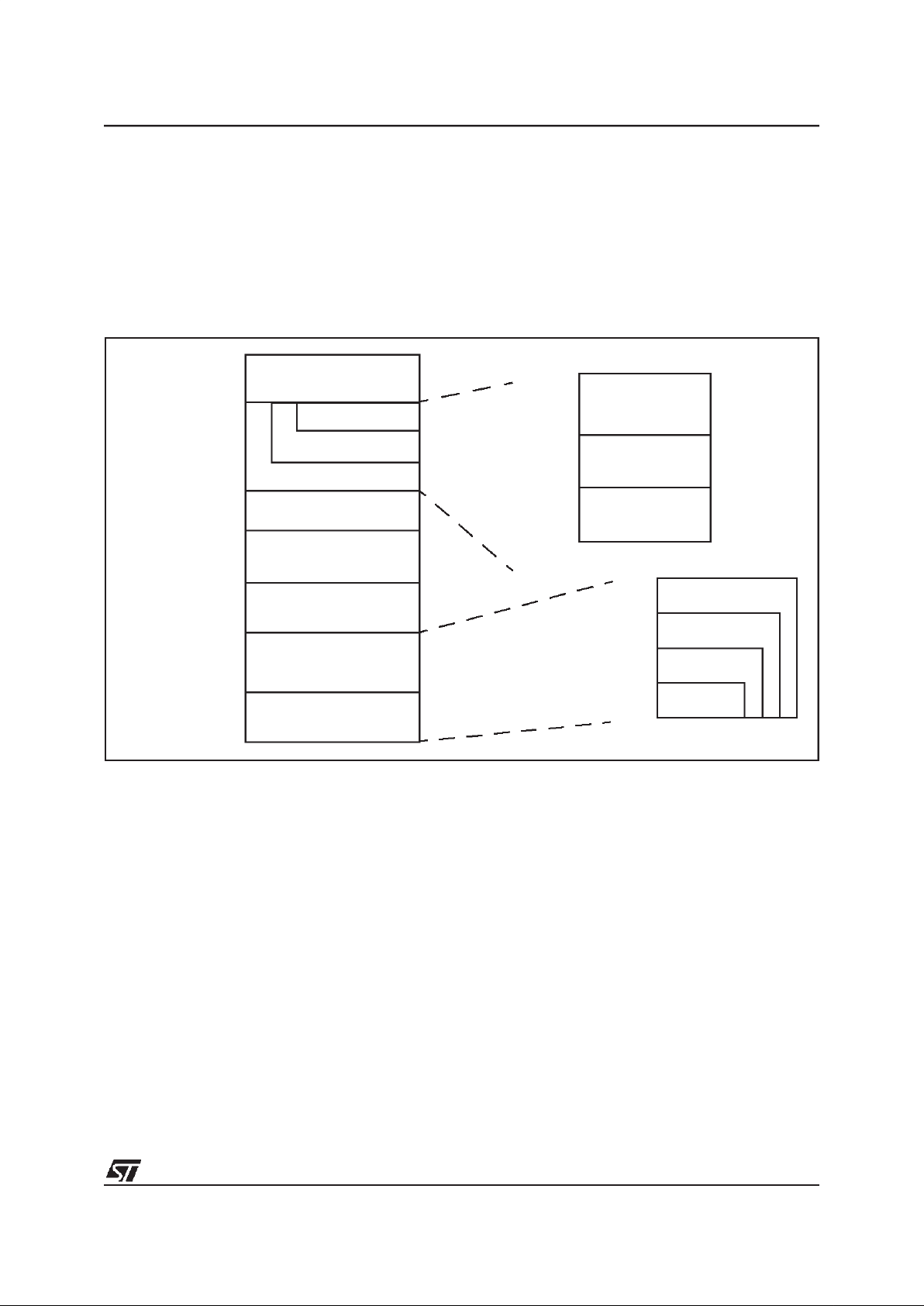
1.3 REGISTER & MEMORY MAP
As shown in the Figure 3, the MCU is capable of
addressing 64K bytes of memories and I/O registers.
The available memory locations consist of 128
bytes of register location, up to 2Kbytes of RAM,
up to 256 bytes of data EEPROM and up to
60Kbytes of user program memory. The RAM
space includes up to 256 bytes for the stack from
0100h to 01FFh.
The highest address bytes contain the user reset
and interrupt vectors.
Figure 3. Memory Map
0000h
1024 Bytes RAM
Program Memory
(60K, 48K, 32K, 16K Bytes)
Interrupt & Reset Vectors
HW Registers
0BFFh
0080h
007Fh
0D00h
0FFFh
Reserved
2048 Bytes RAM
(see Table 2)
1000h
FFDFh
FFE0h
FFFFh
(see Table 7 on page 32)
0C00h
0CFFh
Optional EEPROM
(256 Bytes)
0880h
Reserved
087Fh
Short Addressing
RAM (zero page)
Stack
(256 Bytes)
16-bit Addressing
RAM
0100h
01FFh
047Fh
0080h
0200h
00FFh
or 067Fh
or 087Fh
1536 Bytes RAM
16 KBytes
4000h
1000h
48 KBytes
C000h
8000h
32 KBytes
60 KBytes
FFFFh
ST72311R, ST72511R, ST72512R, ST72532R
12/164
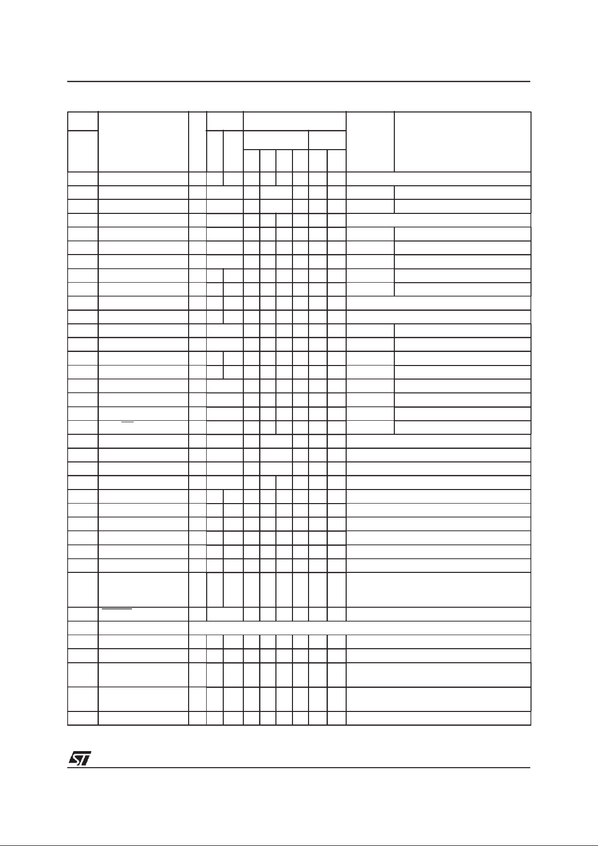
Table 2. Hardware Register Map
Address Block
Register
Label
Register Name
Reset
Status
Remarks
0000h
0001h
0002h
Port A
PADR
PADDR
PAOR
Port A Data Register
Port A Data Direction Register
Port A Option Register
00h
1)
00h
00h
R/W
R/W
R/W
2)
0003h Reserved Area (1 Byte)
0004h
0005h
0006h
Port C
PCDR
PCDDR
PCOR
Port C Data Register
Port C Data Direction Register
Port C Option Register
00h
1)
00h
00h
R/W
R/W
R/W
0007h Reserved Area (1 Byte)
0008h
0009h
000Ah
Port B
PBDR
PBDDR
PBOR
Port B Data Register
Port B Data Direction Register
Port B Option Register
00h
1)
00h
00h
R/W
R/W
R/W
000Bh Reserved Area (1 Byte)
000Ch
000Dh
000Eh
Port E
PEDR
PEDDR
PEOR
Port E Data Register
Port E Data Direction Register
Port E Option Register
00h
1)
00h
00h
R/W
R/W
2)
R/W
2)
000Fh Reserved Area (1 Byte)
0010h
0011h
0012h
Port D
PDDR
PDDDR
PDOR
Port D Data Register
Port D Data Direction Register
Port D Option Register
00h
1)
00h
00h
R/W
R/W
R/W
0013h Reserved Area (1 Byte)
0014h
0015h
0016h
Port F
PFDR
PFDDR
PFOR
Port F Data Register
Port F Data Direction Register
Port F Option Register
00h
1)
00h
00h
R/W
R/W
R/W
0017h
to
001Fh
Reserved Area (9 Bytes)
0020h MISCR1 Miscellaneous Register 1 00h R/W
0021h
0022h
0023h
SPI
SPIDR
SPICR
SPISR
SPI Data I/O Register
SPI Control Register
SPI Status Register
xxh
0xh
00h
R/W
R/W
Read Only
0024h
0025h
0026h
0027h
ITC
ISPR0
ISPR1
ISPR2
ISPR3
Interrupt Software Priority Register 0
Interrupt Software Priority Register 1
Interrupt Software Priority Register 2
Interrupt Software Priority Register 3
FFh
FFh
FFh
FFh
R/W
R/W
R/W
R/W
0028h Reserved Area (1 Byte)
0029h MCC MCCSR Main Clock Control / Status Register 01h R/W

ST72311R, ST72511R, ST72512R, ST72532R
13/164
002Ah
002Bh
WATCHDOG
WDGCR
WDGSR
Watchdog Control Register
Watchdog Status Register
7Fh
000x 000x
R/W
R/W
002Ch EEPROM EECSR Data EEPROM Control/Status Register 00h R/W
002Dh
to
0030h
Reserved Area (4 Bytes)
0031h
0032h
0033h
0034h
0035h
0036h
0037h
0038h
0039h
003Ah
003Bh
003Ch
003Dh
003Eh
003Fh
TIMER A
TACR2
TACR1
TASR
TAIC1HR
TAIC1LR
TAOC1HR
TAOC1LR
TACHR
TACLR
TAACHR
TAACLR
TAIC2HR
TAIC2LR
TAOC2HR
TAOC2LR
Timer A Control Register 2
Timer A Control Register 1
Timer A Status Register
Timer A Input Capture 1 High Register
Timer A Input Capture 1 Low Register
Timer A Output Compare 1 High Register
Timer A Output Compare 1 Low Register
Timer A Counter High Register
Timer A Counter Low Register
Timer A Alternate Counter High Register
Timer A Alternate Counter Low Register
Timer A Input Capture 2 High Register
Timer A Input Capture 2 Low Register
Timer A Output Compare 2 High Register
Timer A Output Compare 2 Low Register
00h
00h
xxh
xxh
xxh
80h
00h
FFh
FCh
FFh
FCh
xxh
xxh
80h
00h
R/W
R/W
Read Only
Read Only
Read Only
R/W
R/W
Read Only
Read Only
Read Only
Read Only
Read Only
Read Only
R/W
R/W
0040h MISCR2 Miscellaneous Register 2 00h R/W
0041h
0042h
0043h
0044h
0045h
0046h
0047h
0048h
0049h
004Ah
004Bh
004Ch
004Dh
004Eh
004Fh
TIMER B
TBCR2
TBCR1
TBSR
TBIC1HR
TBIC1LR
TBOC1HR
TBOC1LR
TBCHR
TBCLR
TBACHR
TBACLR
TBIC2HR
TBIC2LR
TBOC2HR
TBOC2LR
Timer B Control Register 2
Timer B Control Register 1
Timer B Status Register
Timer B Input Capture 1 High Register
Timer B Input Capture 1 Low Register
Timer B Output Compare 1 High Register
Timer B Output Compare 1 Low Register
Timer B Counter High Register
Timer B Counter Low Register
Timer B Alternate Counter High Register
Timer B Alternate Counter Low Register
Timer B Input Capture 2 High Register
Timer B Input Capture 2 Low Register
Timer B Output Compare 2 High Register
Timer B Output Compare 2 Low Register
00h
00h
xxh
xxh
xxh
80h
00h
FFh
FCh
FFh
FCh
xxh
xxh
80h
00h
R/W
R/W
Read Only
Read Only
Read Only
R/W
R/W
Read Only
Read Only
Read Only
Read Only
Read Only
Read Only
R/W
R/W
0050h
0051h
0052h
0053h
0054h
0055h
0056h
0057h
SCI
SCISR
SCIDR
SCIBRR
SCICR1
SCICR2
SCIERPR
SCIETPR
SCI Status Register
SCI Data Register
SCI Baud Rate Register
SCI Control Register 1
SCI Control Register 2
SCI Extended Receive Prescaler Register
Reserved area
SCI Extended Transmit Prescaler Register
C0h
xxh
00xx xxxx
xxh
00h
00h
00h
Read Only
R/W
R/W
R/W
R/W
R/W
R/W
Address Block
Register
Label
Register Name
Reset
Status
Remarks
ST72311R, ST72511R, ST72512R, ST72532R
14/164
Legend: x=undefined, R/W=read/write
Notes:
1. The contents of the I/O port DR registers are readable only in output configuration. In input configuration, the values of the I/O pins are returned instead of the DR register contents.
2. The bits associated with unavailable pins must always keep their reset value.
0058h
0059h
Reserved Area (2 Bytes)
005Ah
005Bh
005Ch
005Dh
005Eh
005Fh
0060h
to
006Fh
CAN
CANISR
CANICR
CANCSR
CANBRPR
CANBTR
CANPSR
CAN Interrupt Status Register
CAN Interrupt Control Register
CAN Control / Status Register
CAN Baud Rate Prescaler Register
CAN Bit Timing Register
CAN Page Selection Register
First address
to
Last address of CAN page X
00h
00h
00h
00h
23h
00h
R/W
R/W
R/W
R/W
R/W
R/W
See CAN
Description
0070h
0071h
ADC
ADCDR
ADCCSR
Data Register
Control/Status Register
xxh
00h
Read Only
R/W
0072h
0073h
0074h
0075h
0076h
0077h
0078h
0079h
PWM ART
PWMDCR3
PWMDCR2
PWMDCR1
PWMDCR0
PWMCR
ARTCSR
ARTCAR
ARTARR
PWM AR Timer Duty Cycle Register 3
PWM AR Timer Duty Cycle Register 2
PWM AR Timer Duty Cycle Register 1
PWM AR Timer Duty Cycle Register 0
PWM AR Timer Control Register
Auto-Reload Timer Control/Status Register
Auto-Reload Timer Counter Access Register
Auto-Reload Timer Auto-Reload Register
00h
00h
00h
00h
00h
00h
00h
00h
R/W
R/W
R/W
R/W
R/W
R/W
R/W
R/W
007Ah
to
007Fh
Reserved Area (6 Bytes)
Address Block
Register
Label
Register Name
Reset
Status
Remarks

ST72311R, ST72511R, ST72512R, ST72532R
15/164
2 EPROM PROGRAM MEMORY
The program memory of the OTP and EPROM devices can be programmed with EPROM programming tools available from STMicroelectronics
EPROM Erasure
EPROM devices are erased by exposure to high
intensity UV light admitted through the transparent
window. This exposure discharges the floating
gate to its initial state through induced photo current.
It is recommended that the EPROM devices be
kept out of direct sunlight, since the UV content of
sunlight can be sufficient to cause functional failure. Extended exposure to room level fluorescent
lighting may also cause erasure.
An opaque coating (paint, tape, label, etc...)
should be placed over the package window if the
product is to be operated under these lighting conditions. Covering the window also reduces IDDin
power-saving modes due to photo-diode leakage
currents.
ST72311R, ST72511R, ST72512R, ST72532R
16/164
3 DATA EEPROM
3.1 INTRODUCTION
The Electrically Erasable Programmable Read
Only Memory can be used as a non volatile backup for storing data. Using theEEPROM requires a
basic access protocol described in this chapter.
3.2 MAIN FEATURES
■ Up to 16 Bytes programmed in the same cycle
■ EEPROM mono-voltage (charge pump)
■ Chained erase and programming cycles
■ Internal control of the global programming cycle
duration
■ End of programming cycle interrupt flag
■ WAIT mode management
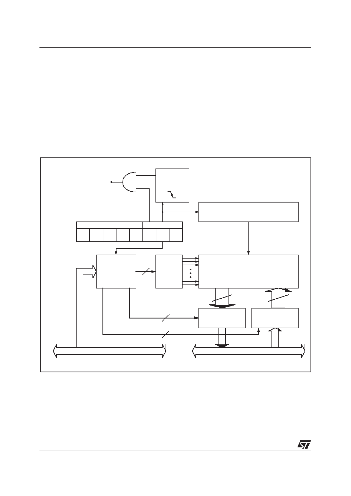
Figure 4. EEPROM Block Diagram
EECSR
EEPROM INTERRUPT
FALLING
EDGE
HIGH VOLTAGE
PUMP
IE LAT00000 PGM
EEPROMRESERVED
DETECTOR
EEPROM
MEMORY MATRIX
(1 ROW = 16 x 8 BITS)
ADDRESS
DECODER
DATA
MULTIPLEXER
16 x 8 BITS
DATA LATCHES
ROW
DECODER
DATA BUS
4
4
4
128128
ADDRESS BUS
ST72311R, ST72511R, ST72512R, ST72532R
17/164
DATA EEPROM (Cont’d)
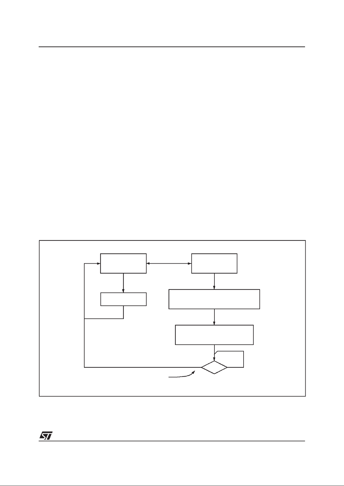
3.3 MEMORY ACCESS
The Data EEPROM memory read/write access
modes are controlled by the LAT bit of the EEPROM Control/Status register (EECSR). The flowchart in Figure 5 describes these different memory
access modes.
Read Operation (LAT=0)
The EEPROM can be read asa normal ROM location when the LAT bit of the EECSR register is
cleared. In a read cycle, the byte to be accessed is
put on the data bus in less than 1 CPU clock cycle.
This means that reading data from EEPROM
takes the same time as reading data from
EPROM, but this memory cannot be used to execute machine code.
Write Operation (LAT=1)
To access the write mode, the LAT bit has to be
set by software (the PGM bit remains cleared).
When a write access to the EEPROM area occurs,
the value is latched inside the 16 data latches according to its address.
When PGM bit is set by the software, all the previous bytes written in the data latches (up to 16) are
programmed in the EEPROM cells. The effective
high address (row) is determined by the last EEPROM write sequence. To avoid wrong programming, the user must take care that all the bytes
written between two programming sequences
have the same high address: only the four Least
Significant Bits of the address can change.
At the end of the programming cycle, the PGM and
LAT bits are cleared simultaneously, and an interrupt is generated if the IE bitis set. The Data EEPROM interrupt request is cleared by hardware
when the Data EEPROM interrupt vector is
fetched.
Note: Care should be taken during the programming cycle. Writing to the same memory location
will over-program the memory (logical AND between the two write access data result) because
the data latches are only cleared at the end of the
programming cycle and by the falling edge of LAT
bit.
It is not possible to read the latched data.
This note is ilustrated by the Figure 6.
Figure 5. Data EEPROM Programming Flowchart
READ MODE
LAT=0
PGM=0
WRITE MODE
LAT=1
PGM=0
READ BYTES
IN EEPROM AREA
WRITE UP TO 16 BYTES
IN EEPROM AREA
(with the same 12 MSB of the address)
START PROGRAMMING CYCLE
LAT=1
PGM=1 (set by software)
LAT
INTERRUPT GENERATION
IF IE=1 0 1
CLEARED BY HARDWARE
ST72311R, ST72511R, ST72512R, ST72532R
18/164
DATA EEPROM (Cont’d)
3.4 POWER SAVING MODES
Wait mode
The DATA EEPROM can enter WAIT mode on execution of the WFI instruction of the microcontroller. The DATA EEPROM will immediately enter
this mode if there is no programming in progress,
otherwise the DATA EEPROM will finish the cycle
and then enter WAIT mode.
Halt mode
The DATA EEPROM immediatly enters HALT
mode if themicrocontroller executes the HALT instruction. Therefore the EEPROM will stop the
function in progress, and data may be corrupted.
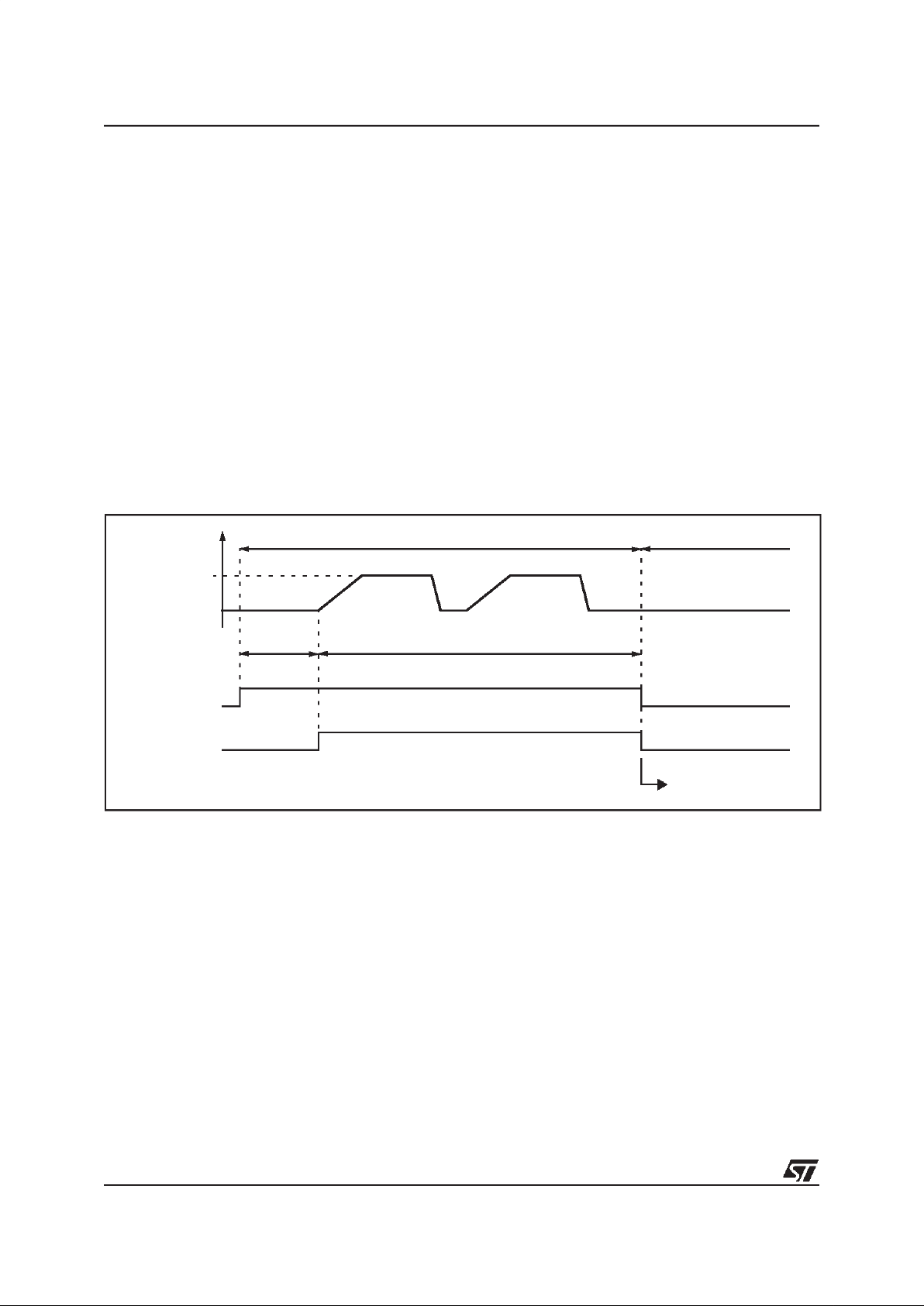
3.5 ACCESS ERROR HANDLING
If a readaccess occurs while LAT=1, thenthe data
bus will not be driven.
If a write access occurs while LAT=0, then the
data on the bus will not be latched.
If a programming cycle is interrupted(by software/
RESET action), the memory data will not be guaranteed.
Figure 6. Data EEPROM Programming Cycle
LAT
ERASE CYCLE WRITE CYCLE
PGM
t
PROG
READ OPERATION NOT POSSIBLE
WRITE OF
DATA LATCHES
READ OPERATION POSSIBLE
INTERNAL
PROGRAMMING
VOLTAGE
EEPROM INTERRUPT

ST72311R, ST72511R, ST72512R, ST72532R
19/164
DATA EEPROM (Cont’d)
3.6 REGISTER DESCRIPTION
CONTROL/STATUS REGISTER (CSR)
Read/Write
Reset Value: 0000 0000 (00h)
Bit 7:3 = Reserved, forced by hardware to 0.
Bit 2 = IE
Interrupt enable
Thisbitisset andclearedby software. Itenablesthe
Data EEPROM interrupt capability when the PGM
bit is cleared byhardware. The interrupt request is
automatically cleared when thesoftware enters the
interrupt routine.
0: Interrupt disabled
1: Interrupt enabled
Bit 1 = LAT
Latch Access Transfer
This bit is set by software. It is cleared by hardware at the end of the programming cycle. It can
only be cleared by software if PGM bit is cleared.
0: Read mode
1: Write mode
Bit 0 = PGM
Programming control and status
Thisbitis set bysoftwaretobegin theprogramming
cycle. At the end of the programming cycle, this bit
isclearedbyhardwareandaninterruptisgenerated
if the ITE bit is set.
0: Programming finished or not yet started
1: Programming cycle is in progress
Note: if the PGM bit is cleared during the programming cycle, the memory data is not guaranteed
Table 3. DATA EEPROM Register Map and Reset Values
70
00000IELATPGM
Address
(Hex.)
Register
Label
76543210
002Ch
EECSR
Reset Value
00000IE0
RWM
0
PGM
0
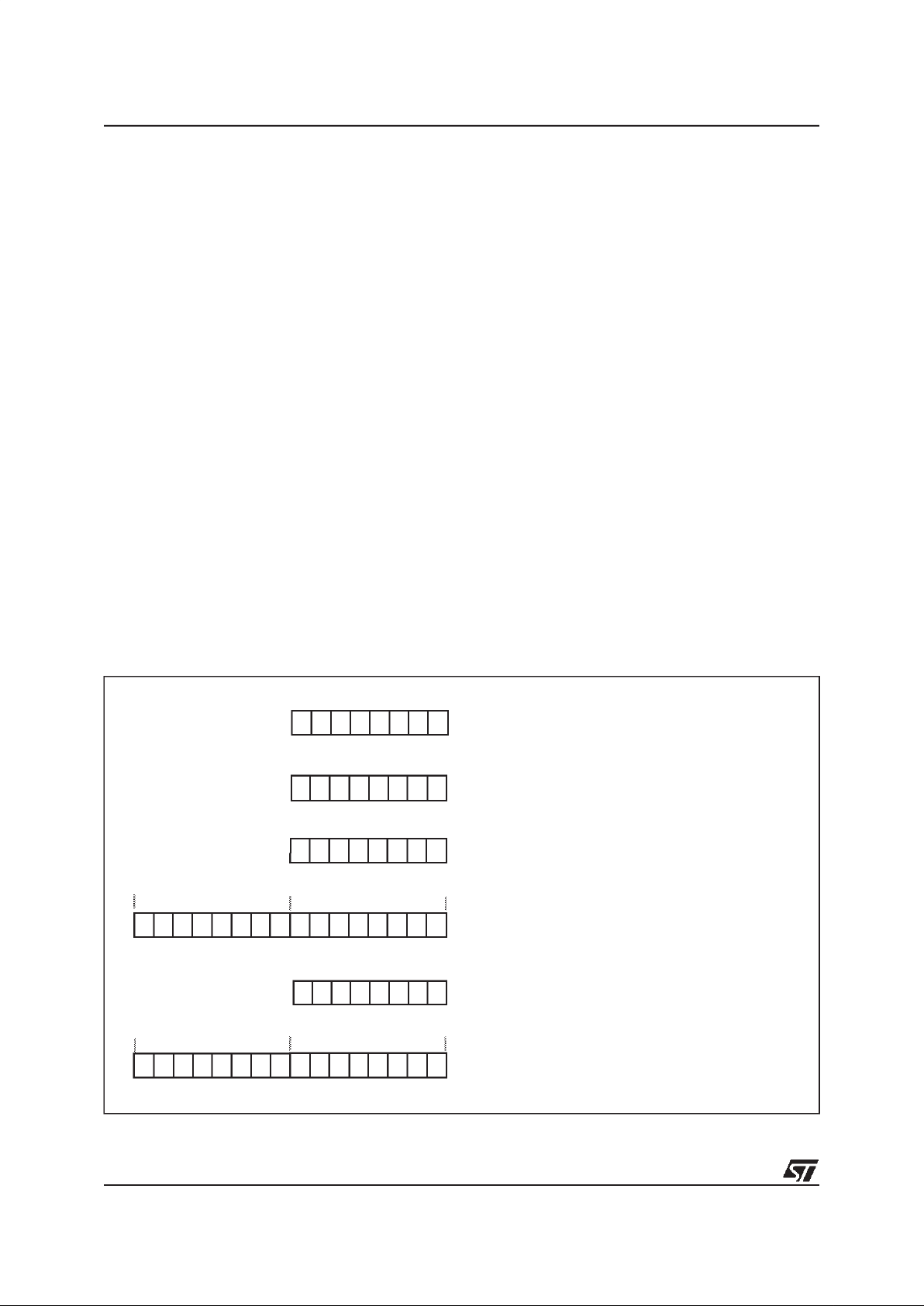
ST72311R, ST72511R, ST72512R, ST72532R
20/164
4 CENTRAL PROCESSING UNIT
4.1 INTRODUCTION
This CPU has a full 8-bit architecture and contains
six internal registers allowing efficient 8-bit data
manipulation.
4.2 MAIN FEATURES
■ Enable executing 63 basic instructions
■ Fast 8-bit by 8-bit multiply
■ 17 main addressing modes (with indirect
addressing mode)
■ Two 8-bit index registers
■ 16-bit stack pointer
■ Low power HALT and WAIT modes
■ Priority maskable hardware interrupts
■ Non-maskable software/hardware interrupts
4.3 CPU REGISTERS
The 6 CPU registers shown in Figure 7 are not
present in the memory mapping andare accessed
by specific instructions.
Accumulator (A)
The Accumulator is an 8-bit general purpose register used to hold operands and the results of the
arithmetic and logic calculations and to manipulate
data.
Index Registers (X and Y)
These 8-bit registers are used to create effective
addresses or as temporary storage areas for data
manipulation. (The Cross-Assembler generates a
precede instruction (PRE) to indicate that the following instruction refers to the Y register.)
The Y register is not affected by theinterrupt automatic procedures.
Program Counter (PC)
The programcounter is a 16-bit register containing
the address of the next instruction to be executed
by the CPU. It is made of two 8-bit registers PCL
(Program CounterLow which is the LSB) and PCH
(Program Counter High which is the MSB).
Figure 7. CPU Registers
ACCUMULATOR
X INDEX REGISTER
Y INDEX REGISTER
STACK POINTER
CONDITION CODE REGISTER
PROGRAM COUNTER
70
1C1I1HI0NZ
RESET VALUE = RESET VECTOR @ FFFEh-FFFFh
70
70
70
0
715 8
PCH
PCL
15
87 0
RESET VALUE = STACKHIGHER ADDRESS
RESET VALUE =
1X11X1XX
RESET VALUE = XXh
RESET VALUE = XXh
RESET VALUE= XXh
X = Undefined Value
ST72311R, ST72511R, ST72512R, ST72532R
21/164
CENTRAL PROCESSING UNIT (Cont’d)
Condition Code Register (CC)
Read/Write
Reset Value: 111x1xxx
The 8-bit Condition Code register contains the interrupt masks and four flags representative of the
result of the instruction just executed. This register
can also be handled by the PUSH and POP instructions.
These bits can be individually tested and/or controlled by specific instructions.
Arithmetic management bits
Bit 4 = H
Half carry
.
This bit is set by hardware whena carry occurs between bits 3 and 4 of the ALU during an ADD or
ADC instructions. It is reset by hardware during
the same instructions.
0: No half carry has occurred.
1: An half carry has occurred.
This bit is tested using the JRH or JRNH instruction. The H bit is useful in BCD arithmetic subroutines.
Bit 2 = N
Negative
.
This bit is set and cleared by hardware. It is representative of the result sign of the last arithmetic,
logical or data manipulation. It’s a copy of the result 7thbit.
0: Theresult of the last operation ispositive or null.
1: The result of the last operation is negative
(i.e. the most significant bit is a logic 1).
This bit is accessed by the JRMI and JRPLinstructions.
Bit 1 = Z
Zero
.
This bit is set and cleared by hardware. This bit indicates that the result of the last arithmetic, logical
or data manipulation is zero.
0: The result of the last operation is different from
zero.
1: The result of the last operation is zero.
This bit is accessed by the JREQ and JRNE test
instructions.
Bit 0 = C
Carry/borrow.
This bit is set and cleared by hardware and software. It indicates an overflow or an underflow has
occurred during the last arithmetic operation.
0: No overflow or underflow has occurred.
1: An overflow or underflow has occurred.
This bit is driven by the SCF and RCF instructions
and tested by theJRC and JRNC instructions. It is
also affected by the “bit test and branch”, shift and
rotate instructions.
Interrupt management bits
Bit 5,3 = I1, I0
Interrupt.
The combination of the Iand I0 bits gives the current interrupt software priority.
These two bits are set/cleared by hardware when
entering in interrupt. The loaded value is given by
the corresponding bits in the interrupt software priority registers (IxSPR). They can be also set/
cleared by software with the RIM, SIM, IRET,
HALT, WFI and PUSH/POP instructions.
See the interrupt management chapter for more
details.
70
11I1HI0NZ
C
Interrupt SoftwarePriority I1 I0
Level 0 (main) 1 0
Level 1 0 1
Level 2 0 0
Level 3 (= interrupt disable) 1 1
ST72311R, ST72511R, ST72512R, ST72532R
22/164
CENTRAL PROCESSING UNIT (Cont’d)
Stack Pointer (SP)
Read/Write
Reset Value: 01 FFh
The Stack Pointer is a 16-bit register which is always pointing to the next free location in the stack.
It is then decremented after data has been pushed
onto the stack and incremented before data is
popped from the stack (see Figure 8).
Since the stack is 256 bytes deep, the 8 most significant bits are forced by hardware. Following an
MCU Reset, or after a Reset Stack Pointer instruction (RSP), the Stack Pointer contains its reset value (the SP7 to SP0 bits are set) which is the stack
higher address.
The least significant byte of the Stack Pointer
(called S) can be directly accessed by a LD instruction.
Note: When the lower limit is exceeded, the Stack
Pointer wraps around to the stackupper limit, without indicating the stack overflow. The previously
stored information is then overwritten and therefore lost.The stack also wraps in caseof anunderflow.
The stack is used to save the return address during a subroutine call and the CPU context during
an interrupt. The user may also directly manipulate
the stack by means of the PUSH and POP instructions. In the case of an interrupt, the PCL is stored
at the first location pointed to by the SP. Then the
other registers are stored in the next locations as
shown in Figure 8
– When an interrupt is received, the SP is decre-
mented and the context is pushed on the stack.
– On return frominterrupt, the SP is incremented
and the context is popped from the stack.
A subroutine call occupies twolocations and an interrupt five locations in the stack area.
Figure 8. Stack Manipulation Example
15 8
00000001
70
SP7 SP6 SP5 SP4 SP3 SP2 SP1 SP0
PCH
PCL
SP
PCH
PCL
SP
PCL
PCH
X
A
CC
PCH
PCL
SP
PCL
PCH
X
A
CC
PCH
PCL
SP
PCL
PCH
X
A
CC
PCH
PCL
SP
SP
Y
CALL
Subroutine
Interrupt
Event
PUSH Y POP Y IRET
RET
or RSP
@ 01FFh
@ 0100h
Stack Higher Address = 01FFh
Stack Lower Address =
0100h
ST72311R, ST72511R, ST72512R, ST72532R
23/164
5 SUPPLY, RESET AND CLOCK MANAGEMENT
The ST72311R, ST72511R, ST72512R and
ST72532R microcontrollers include a range of utility features for securing the application in critical
situations (for example in case of a power brownout), and reducing the number of external components. An overview is shown in Figure 9.
Main features
■ Main supply low voltage detection (LVD)
■ RESET Manager (RSM)
■ Low consumption resonator oscillator
Figure 9. Clock, RESET, Option and Supply Management Overview
f
OSC
LOW VOLTAGE
DETECTOR
(LVD)
FROM
WATCHDOG
PERIPHERAL
OSC2
OSC1
RESET
V
DD
V
SS
OSCILLATOR
RESET
TO
MAIN CLOCK
CONTROLLER
ST72311R, ST72511R, ST72512R, ST72532R
24/164
5.1 LOW VOLTAGE DETECTOR (LVD)
To allow the integration of power management
features in theapplication, the Low Voltage Detector function (LVD) generates a static reset when
the VDDsupply voltage is below a V
IT-
reference
value. This means that it secures the power-up as
well as the power-down keeping the ST7 in reset.
The V
IT-
referencevalue for a voltage drop is lower
than the V
IT+
referencevalue for power-on in order
to avoida parasitic reset when theMCU starts running and sinks current on the supply (hysteresis).
The LVD Reset circuitry generates a reset when
VDDis below:
–V
IT+
when VDDis rising
–V
IT-
when VDDis falling
The LVD function is illustrated in Figure 10.
Provided the minimum VDDvalue (guaranteed for
the oscillator frequency) is below V
IT-
, the MCU
can onlybe in two modes:
– under full software control
– in static safe reset
In these conditions, secure operation is always ensured for the application without the need for external reset hardware.
During a Low Voltage Detector Reset, the RESET
pin is held low, thus permitting the MCU to reset
other devices.
Notes:
The LVD allows the device to be used without any
external RESET circuitry.
The LVD is an optional function which can be se-
lected whenordering the device (ordering information).
Figure 10. Low Voltage Detector vs Reset
V
DD
V
IT+
RESET
V
IT-
V
hys
ST72311R, ST72511R, ST72512R, ST72532R
25/164
5.2 RESET SEQUENCE MANAGER (RSM)
5.2.1 Introduction
The reset sequence manager includes three RESET sources as shown in Figure 12:
■ External RESET source pulse
■ Internal LVD RESET (Low Voltage Detection)
■ Internal WATCHDOG RESET
These sources act on the RESET pin and it is always kept low during the delay phase.
The RESET service routine vector is fixed at addresses FFFEh-FFFFh in the ST7 memory map.
The basic RESET sequence consists of 3 phases
as shown in Figure11:
■ Delay depending on the RESET source
■ 4096 CPU clock cycle delay
■ RESET vector fetch
The 4096 CPU clock cycle delay allows the oscillator to stabilise and ensures that recovery has
taken place from the Reset state.
The RESET vector fetch phase duration is 2 clock
cycles.
Figure 11. RESET Sequence Phases
Figure 12. Reset Block Diagram
RESET
DELAY
INTERNAL RESET
4096 CLOCKCYCLES
FETCH
VECTOR
f
CPU
COUNTER
RESET
R
ON
V
DD
WATCHDOG RESET
LVD RESET
INTERNAL
RESET
ST72311R, ST72511R, ST72512R, ST72532R
26/164
RESET SEQUENCE MANAGER (Cont’d)
5.2.2 Asynchronous External RESET pin
The RESET pin is both an input andan open-drain
output with integrated RONweak pull-up resistor.
This pull-up has no fixed value but varies in accordance with the input voltage. It can be pulled
low by external circuitry to reset the device. See
electrical characteristics section for more details.
A RESET signal originating from an external
source must have a duration of atleast t
h(RSTL)in
in
order to berecognized as shown in Figure 13. This
detection is asynchronous and therefore the MCU
can enterreset state even in HALT mode.
The RESET pin is an asynchronous signal which
plays a major role in EMS performance. In a noisy
environment, it is recommended to follow the
guidelines mentioned in the electrical characteristics section.
5.2.3 Internal Low Voltage Detection RESET
Two different RESET sequences caused by the internal LVD circuitry can be distinguished:
■ Power-On RESET
■ Voltage Drop RESET
The device RESET pin acts as an output that is
pulled low when VDD<V
IT+
(rising edge) or
VDD<V
IT-
(falling edge)as shown in Figure 13.
The LVD filters spikes on VDDlarger than t
g(VDD)
to
avoid parasitic resets.
5.2.4 Internal WatchdogRESET
The RESET sequence generated by a internal
Watchdog counter overflow is shown in Figure 13.
Starting fromthe Watchdog counter underflow, the
device RESET pin acts as an output that is pulled
low during t
w(RSTL)out
.
CAUTION: this output signal as not enought energy to be used to drive external devices.
Figure 13. RESET Sequences
V
DD
RUN
RESET PIN
EXTERNAL
WATCHDOG
DELAY
V
IT+
V
IT-
t
h(RSTL)in
RUN
DELAY
WATCHDOG UNDERFLOW
t
w(RSTL)out
RUN
DELAY
RUN
RESET
RESET
SOURCE
SHORT EXT.
RESET
LVD
RESET
WATCHDOG
RESET
INTERNAL RESET (4096T
CPU
)
FETCH VECTOR
ST72311R, ST72511R, ST72512R, ST72532R
27/164
5.3 LOW CONSUMPTION OSCILLATOR
The f
OSC
main clock of the ST7 can be generated
by two different source types:
■ an external source
■ a crystal or ceramic resonator oscillators
The associated hardware configuration are shown
in Table 4. Refer to the electrical characteristics
section for more details.
External Clock Source
In this external clock mode, a clock signal (square,
sinus or triangle) with ~50% duty cycle has to drive
the OSC1pin while the OSC2 pinis tied to ground.
Crystal/Ceramic Oscillator
This oscillator (based on constant current source)
is optimized in terms of consumption and has the
advantage of producing a very accurate rate on
the main clock of the ST7.
When using this oscillator, the resonator and the
load capacitances have to be connected as shown
in Table 4 and have to be mounted as close as
possible to the oscillator pins in order to minimize
output distortion and start-up stabilization time.
This oscillator is not stopped during the RESET
phase to avoid losing time in the oscillator start-up
phase.
These oscillators are not stopped during the
RESET phase to avoid losing time in the oscillator
start-up phase.
Table 4. ST7 Clock Sources
Hardware Configuration
External ClockCrystal/Ceramic Resonators
OSC1 OSC2
EXTERNAL
ST7
SOURCE
V
DD
R
OBP
OSC1 OSC2
LOAD
CAPACITORS
ST7
C
L2
C
L1
ST72311R, ST72511R, ST72512R, ST72532R
28/164
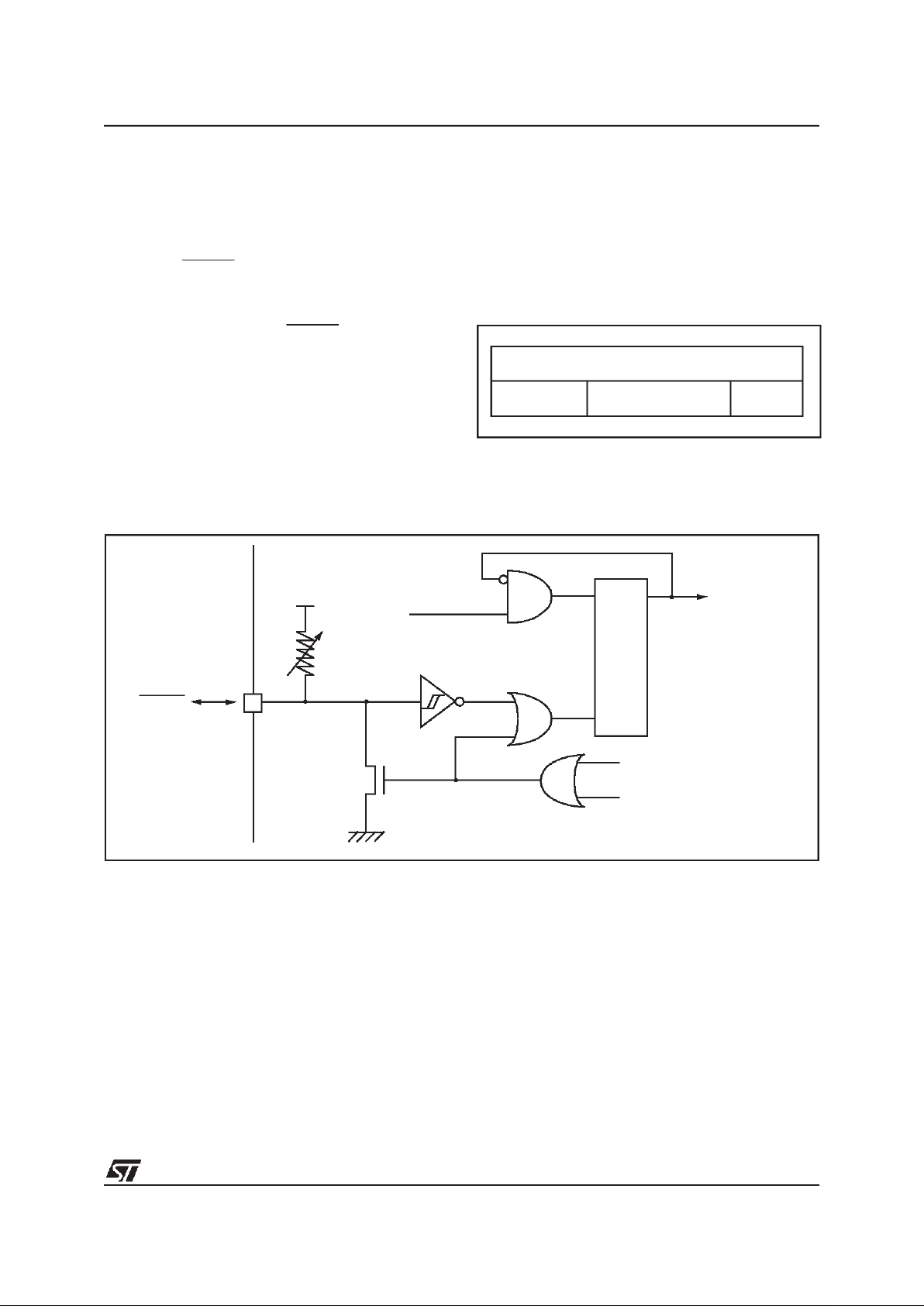
6 INTERRUPTS
6.1 INTRODUCTION
The ST7 enhanced interrupt management provides the following features:
■ Hardware interrupts
■ Software interrupt (TRAP)
■ Nested or concurrent interrupt management
with flexible interrupt priority and level
management:
– Up to 4 software programmable nesting levels
– Up to 16 interrupt vectors fixed by hardware
– 3 non maskable events: TLI, RESET, TRAP
This interrupt management is based on:
– Bit 5 and bit 3 of the CPU CC register (I1:0),
– Interrupt software priority registers (ISPRx),
– Fixed interrupt vector addresses located at the
high addresses of the memory map (FFE0h to
FFFFh) sorted by hardware priority order.
This enhanced interrupt controller guarantees full
upward compatibility with the standard (not nested) ST7 interrupt controller.
6.2 MASKING AND PROCESSING FLOW
The interrupt masking is managed by the I1and I0
bits of the CC register and the ISPRx registers
which give the interrupt software priority level of
each interrupt vector (see Table 5). The processing flow is shown in Figure 14
When an interrupt request has to be serviced:
– Normal processing is suspended at the end of
the current instruction execution.
– The PC, X, A and CC registers are saved onto
the stack.
– I1 and I0 bits of CC register are set according to
the corresponding values in the ISPRx registers
of the serviced interrupt vector.
– ThePC isthen loadedwith the interrupt vector of
the interrupt to service and the first instruction of
the interrupt service routine is fetched (refer to
“Interrupt Mapping” table for vector addresses).
The interrupt service routine should end with the
IRET instruction which causes the contents of the
saved registers to be recovered from the stack.
Note: As a consequence of the IRET instruction,
the I1 and I0 bits will be restored from the stack
and the program in the previous level will resume.
Table 5. Interrupt Software Priority Levels
Figure 14. Interrupt Processing Flowchart
Interrupt software priority Level I1 I0
Level 0 (main) Low
High
10
Level 1 0 1
Level 2 0 0
Level 3 (= interrupt disable) 1 1
“IRET”
RESTORE PC,X, A,CC
STACK PC, X, A, CC
LOAD I1:0 FROM INTERRUPT SW REG.
FETCH NEXT
RESET
TLI
PENDING
INSTRUCTION
I1:0
FROM STACK
LOAD PC FROM INTERRUPT VECTOR
Y
N
Y
N
Y
N
Interrupt has the same or a
lower software priority
THE INTERRUPT
STAYS PENDING
than current one
Interrupt has a higher
software priority
than current one
EXECUTE
INSTRUCTION
INTERRUPT
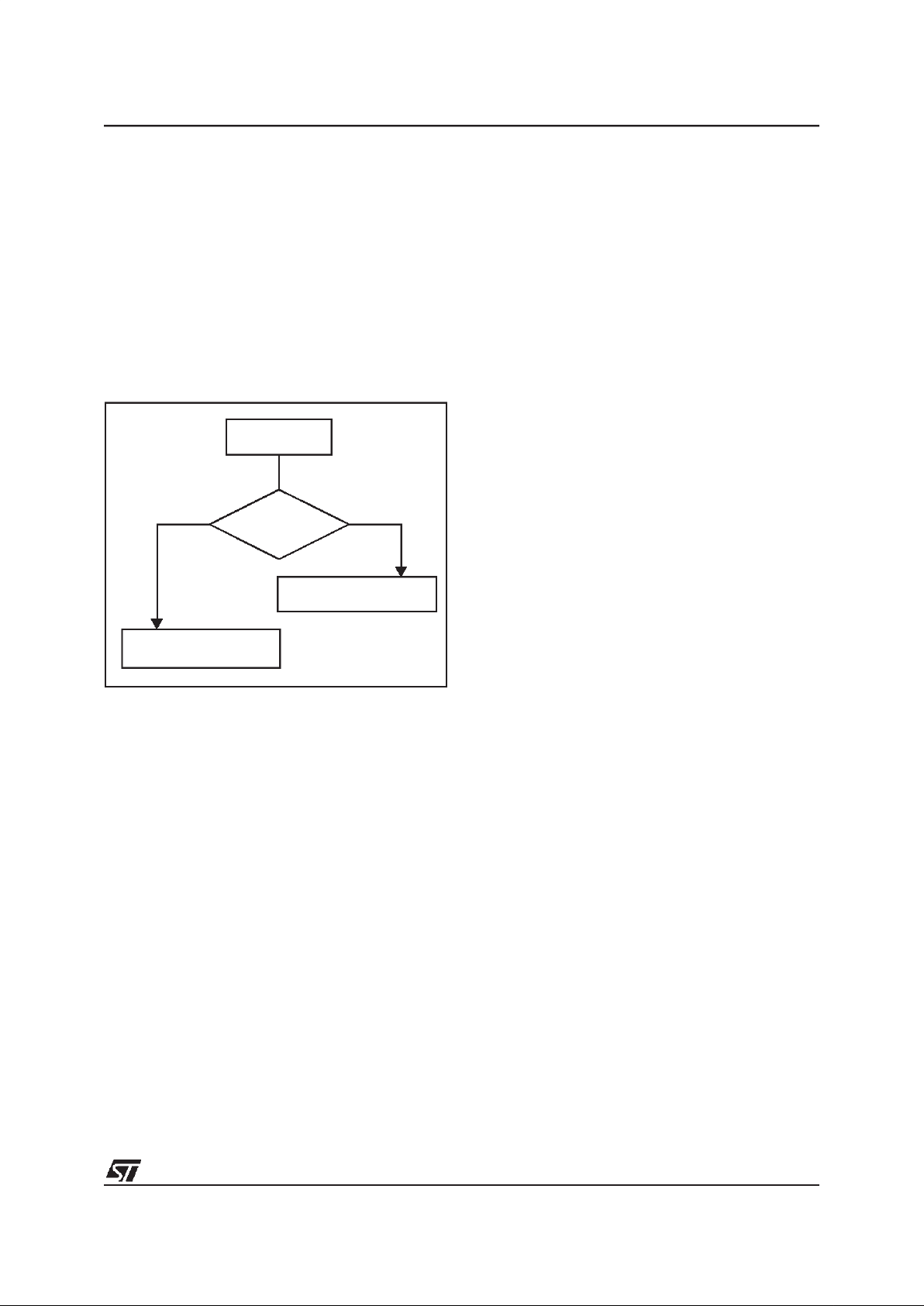
ST72311R, ST72511R, ST72512R, ST72532R
29/164
INTERRUPTS (Cont’d)
Servicing Pending Interrupts
As several interrupts can be pending at the same
time, theinterrupt to be taken into account is determined by the following two-step process:
– the highestsoftware priority interrupt is serviced,
– if several interrupts have the same software pri-
ority thenthe interrupt with the highest hardware
priority is serviced first.
Figure 15 describes this decision process.
Figure 15. Priority Decision Process
When an interrupt request is not serviced immediately, it is latched and then processed when its
software priority combined with the hardware priority becomes the highest one.
Note 1: The hardware priority is exclusive while
the software one is not. This allows the previous
process to succeed with only one interrupt.
Note 2: RESET, TRAP and TLI are non maskable
and they can be considered as having the highest
software priority in the decision process.
Different Interrupt Vector Sources
Two interrupt source types are managed by the
ST7 interrupt controller: the non-maskable type
(RESET, TLI, TRAP) and the maskable type (external or from internal peripherals).
Non-Maskable Sources
These sources are processed regardless of the
state of the I1 and I0 bits of the CC register (see
Figure 14). After stacking the PC, X, A and CC
registers (except for RESET), the corresponding
vector is loaded in the PC register and the I1 and
I0 bits of the CC are set to disable interrupts (level
3). These sources allow the processor to exit
HALT mode.
■ TLI (Top Level Hardware Interrupt)
This hardware interrupt occurs when a specific
edge is detected on the dedicated TLI pin. Its detailed specification is given in the Miscellaneous
register chapter.
■ TRAP (Non Maskable Software Interrupt)
This software interrupt is serviced when the TRAP
instruction is executed. It will be serviced according to the flowchart on Figure 14 as a TLI.
■ RESET
The RESET source has the highest priority in the
ST7. This means that the first current routine has
the highest software priority (level 3) and thehighest hardware priority.
See the RESET chapter for more details.
Maskable Sources
Maskable interrupt vector sourcescan be serviced
if the corresponding interrupt is enabled and if its
own interrupt software priority (in ISPRx registers)
is higher than the one currently being serviced (I1
and I0 in CC register). If any of these two conditions is false, the interrupt is latched and thus remains pending.
■ External Interrupts
External interrupts allow the processor to exit from
HALT low power mode.
External interrupt sensitivity is softwareselectable
through the Miscellaneous registers (MISCRx).
External interrupt triggeredon edge will be latched
and the interrupt request automatically cleared
upon entering the interrupt service routine.
If several input pins of a group connected to the
same interrupt line are selected simultaneously,
these will be logically ORed.
■ Peripheral Interrupts
Usually the peripheral interrupts cause the MCU to
exit from HALT mode except those mentioned in
the “Interrupt Mapping” table.
A peripheral interrupt occurs when a specific flag
is set in the peripheral status registers and if the
corresponding enable bit is set in the peripheral
control register.
The general sequence for clearing an interrupt is
based on an access to the status register followed
by a read or write to an associated register.
Note: The clearing sequence resets the internal
latch. A pending interrupt (i.e. waiting for being
serviced) will therefore be lost if the clear sequence is executed.
PENDING
SOFTWARE
Different
INTERRUPTS
Same
HIGHESTHARDWARE
PRIORITY SERVICED
PRIORITY
HIGHEST SOFTWARE
PRIORITY SERVICED
ST72311R, ST72511R, ST72512R, ST72532R
30/164
INTERRUPTS (Cont’d)
6.3 INTERRUPTS AND LOW POWER MODES
All interrupts allow the processor to exit the WAIT
low power mode. On the contrary, only external
and other specified interrupts allow the processor
to exit the HALT modes (see column “Exit from
HALT” in“Interrupt Mapping” table). When several
pending interrupts are present while exiting HALT
mode, the first one serviced can only be an interrupt with exit from HALT mode capability and it is
selected through the same decision process
shown in Figure 15
Note: If an interrupt, that is not able to Exit from
HALT mode, is pending with the highest priority
when exiting HALT mode, this interrupt is serviced
after the first one serviced.
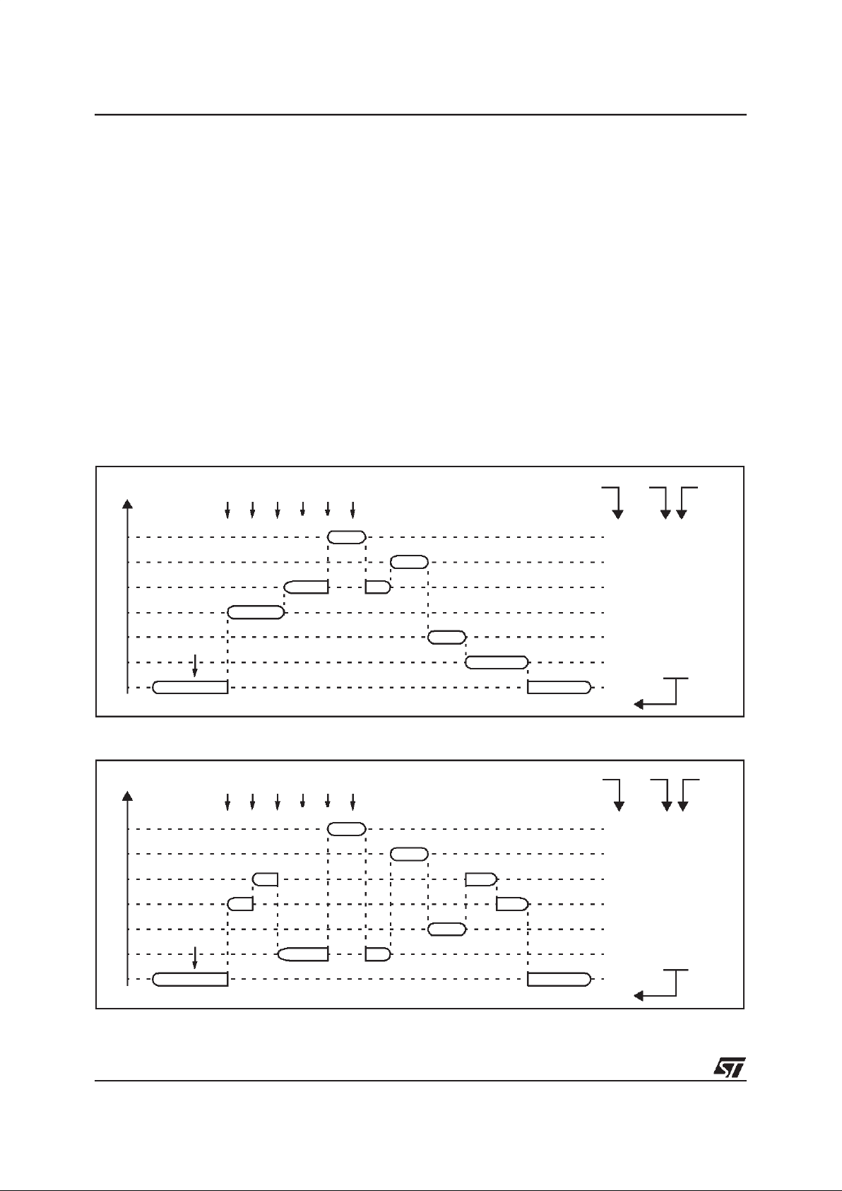
6.4 CONCURRENT & NESTED MANAGEMENT
The following Figure 16 and Figure 17 show two
different interrupt management modes. The first is
called concurrent mode and does not allow an interrupt to be interrupted, unlike the nested mode in
Figure 17 The interrupt hardware priority is given
in this order from the lowest to the highest: MAIN,
IT4, IT3, IT2, IT1, IT0,TLI. The software priority is
given for each interrupt.
Warning: A stack overflow may occur without notifying the software of the failure.
Figure 16. Concurrent interrupt management
Figure 17. Nested interrupt management
MAIN
IT4
IT2
IT1
TLI
IT1
MAIN
IT0
I1
HARDWARE PRIORITY
SOFTWARE
3
3
3
3
3
3/0
3
11
11
11
11
11
11 / 10
11
RIM
IT2
IT1
IT4
TLI
IT3
IT0
IT3
I0
10
PRIORITY
LEVEL
USED STACK = 10 BYTES
MAIN
IT2
TLI
MAIN
IT0
IT2
IT1
IT4
TLI
IT3
IT0
HARDWARE PRIORITY
3
2
1
3
3
3/0
3
11
00
01
11
11
11
RIM
IT1
IT4 IT4
IT1
IT2
IT3
I1 I0
11 / 10 10
SOFTWARE
PRIORITY
LEVEL
USED STACK = 20 BYTES
 Loading...