

SGS Thomson Microelectronics ST72E631K4D0 Datasheet
ST7263
LOW SPEED USB 8-BIT MCU F AMILY with up to 16K MEMORY,
up to 512 BYTES RAM, 8-BIT ADC, WDG, TIMER, SCI
■ Up to 16Kbytes program memory
■ Data RAM: up to 512 bytes with 64 bytes stack
■ Run, Wait and Halt CPU modes
■ 12 or 24 MH z os c illator
■ RAM retention mode
■ USB (Universal Serial Bus) Interface with DMA
for low speed applications compliant with USB
1.5 Mbs specification (version 1.1) and USB
HID specifications (version 1.0)
■ Integrated 3.3V voltage regulator and
transceivers
■ Suspend and Resume operations
■ 3 endpoints with programmable in/out
configuration
■ 19 programmable I/O lines with:
– 8 high current I/Os (10mA at 1.3V)
– 2 very high current pure Open Drain I/Os
(25mA at 1.5V)
– 8 lines individually programmable as interrupt
inputs
■ Optional Low Voltage Detector (LVD)
■ Programmable Watchdog for system reliability
■ 16-bit Timer with:
– 2 Input Captures
– 2 Output Compares
– PWM Generation capabilities
– External Clock input
■ Asynchronous Serial Communications Interface
(8K and 16K program memory versions only)
2
■ I
C Multi Master Interface up to 400 KHz
(16K program memory version only)
■ 8-bit A/D Converter (ADC) with 8 channels
■ Fully static operation
■ 63 basic instructions
■ 17 main addressing modes
■ 8x8 unsigned multiply instruction
■ True bit manipulation
■ Versatile Development Tools (und er Windows)
including assembler, linker, C-compiler,
archiver, source level debugger, software
library, hardware emulator, programming
boards and gang programmers
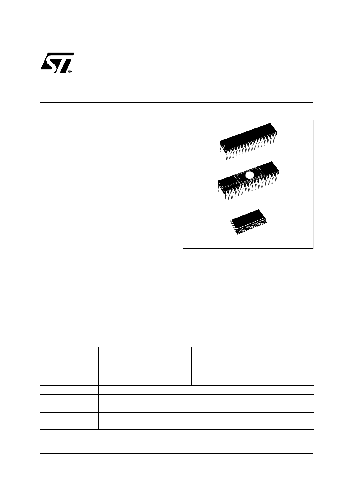
PSDIP32
CSDIP32W
SO34 (Shrink)
& I2C
DATASHEET
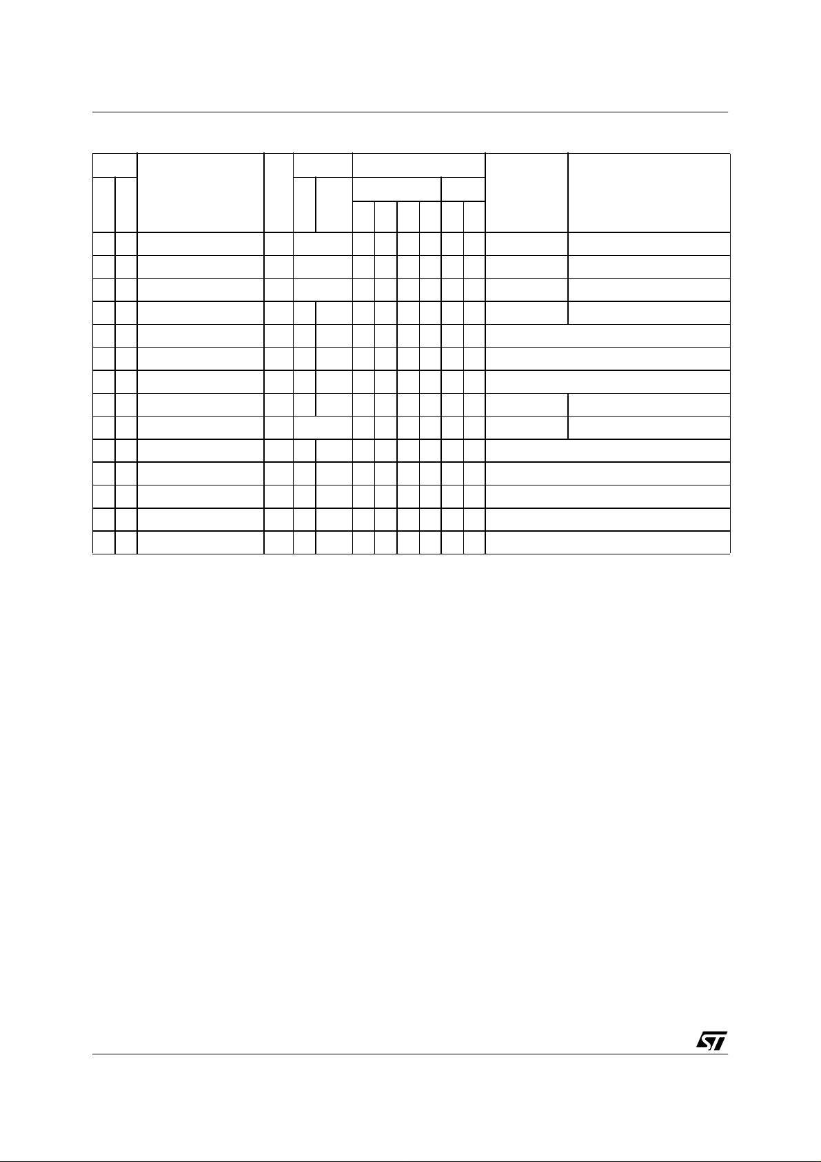
Table 1. Device Summary
Features
ROM - OTP (bytes) 16K 8K 4K
RAM (stack) - bytes 512 (64) 256 (64)
Peripherals
Operating Supply 4.0V to 5.5V
CPU frequency 8 Mhz (with 24 MHz oscillator) or 4 MHz (with 12 MHz oscillator)
Operating temperature 0°C to +70°C
Packages SO34/SDIP32
EPROM device ST72E631
Watchdog, 16-bit timer, SCI, I
Note 1: EPROM version for development only
August 2000 1/109
ST72631
USB
2
C, ADC,
ST72632 ST72633
Watchdog, 16-bit timer,
SCI, ADC, USB
1
(CSDIP32W)
Watchdog, 16-bit timer,
ADC, USB
Rev. 1.8
1

Table of Contents
1 GENERAL DESCRIPTION . . . . . . . . . . . . . . . . . . . . . . . . . . . . . . . . . . . . . . . . . . . . . . . . . . . . . . 5
1.1 INTRODUCTION . . . . . . . . . . . . . . . . . . . . . . . . . . . . . . . . . . . . . . . . . . . . . . . . . . . . . . . . . 5
1.2 PIN DESCRIPTION . . . . . . . . . . . . . . . . . . . . . . . . . . . . . . . . . . . . . . . . . . . . . . . . . . . . . . . 6
1.3 EXTERNAL CONNECTIONS . . . . . . . . . . . . . . . . . . . . . . . . . . . . . . . . . . . . . . . . . . . . . . . . 9
1.4 REGISTER & MEMORY MAP . . . . . . . . . . . . . . . . . . . . . . . . . . . . . . . . . . . . . . . . . . . . . . 10
1.5 EPROM/OTP PROGRAM MEMORY . . . . . . . . . . . . . . . . . . . . . . . . . . . . . . . . . . . . . . . . . 13
1.5.1 EPROM ERASURE . . . . . . . . . . . . . . . . . . . . . . . . . . . . . . . . . . . . . . . . . . . . . . . . . 13
2 CENTRAL PROCESSING UNIT . . . . . . . . . . . . . . . . . . . . . . . . . . . . . . . . . . . . . . . . . . . . . . . . . 14
2.1 INTRODUCTION . . . . . . . . . . . . . . . . . . . . . . . . . . . . . . . . . . . . . . . . . . . . . . . . . . . . . . . . 14
2.2 MAIN FEATURES . . . . . . . . . . . . . . . . . . . . . . . . . . . . . . . . . . . . . . . . . . . . . . . . . . . . . . . 14
2.3 CPU REGISTERS . . . . . . . . . . . . . . . . . . . . . . . . . . . . . . . . . . . . . . . . . . . . . . . . . . . . . . . 14
3 CLOCKS AND RESET . . . . . . . . . . . . . . . . . . . . . . . . . . . . . . . . . . . . . . . . . . . . . . . . . . . . . . . . 17
3.1 CLOCK SYSTEM . . . . . . . . . . . . . . . . . . . . . . . . . . . . . . . . . . . . . . . . . . . . . . . . . . . . . . . . 17
3.1.1 General Description . . . . . . . . . . . . . . . . . . . . . . . . . . . . . . . . . . . . . . . . . . . . . . . . . 17
3.1.2 External Clock . . . . . . . . . . . . . . . . . . . . . . . . . . . . . . . . . . . . . . . . . . . . . . . . . . . . . 17
3.2 RESET . . . . . . . . . . . . . . . . . . . . . . . . . . . . . . . . . . . . . . . . . . . . . . . . . . . . . . . . . . . . . . . . 18
3.2.1 Low Voltage Detector (LVD) . . . . . . . . . . . . . . . . . . . . . . . . . . . . . . . . . . . . . . . . . . 18
3.2.2 Watchdog Reset . . . . . . . . . . . . . . . . . . . . . . . . . . . . . . . . . . . . . . . . . . . . . . . . . . . 18
3.2.3 External Reset . . . . . . . . . . . . . . . . . . . . . . . . . . . . . . . . . . . . . . . . . . . . . . . . . . . . . 18
4 INTERRUPTS AND POWER SAVING MODES . . . . . . . . . . . . . . . . . . . . . . . . . . . . . . . . . . . . . 20
4.1 INTERRUPTS . . . . . . . . . . . . . . . . . . . . . . . . . . . . . . . . . . . . . . . . . . . . . . . . . . . . . . . . . . 20
4.1.1 Interrupt Register . . . . . . . . . . . . . . . . . . . . . . . . . . . . . . . . . . . . . . . . . . . . . . . . . . . 22
4.2 POWER SAVING MODES . . . . . . . . . . . . . . . . . . . . . . . . . . . . . . . . . . . . . . . . . . . . . . . . . 23
4.2.1 Introduction . . . . . . . . . . . . . . . . . . . . . . . . . . . . . . . . . . . . . . . . . . . . . . . . . . . . . . . 23
4.2.2 HALT mode . . . . . . . . . . . . . . . . . . . . . . . . . . . . . . . . . . . . . . . . . . . . . . . . . . . . . . . 23
4.2.3 WAIT mode . . . . . . . . . . . . . . . . . . . . . . . . . . . . . . . . . . . . . . . . . . . . . . . . . . . . . . . 24
5 ON-CHIP PERIPHERALS . . . . . . . . . . . . . . . . . . . . . . . . . . . . . . . . . . . . . . . . . . . . . . . . . . . . . . 25
5.1 I/O PORTS . . . . . . . . . . . . . . . . . . . . . . . . . . . . . . . . . . . . . . . . . . . . . . . . . . . . . . . . . . . . . 25
5.1.1 Introduction . . . . . . . . . . . . . . . . . . . . . . . . . . . . . . . . . . . . . . . . . . . . . . . . . . . . . . . 25
5.1.2 Functional description . . . . . . . . . . . . . . . . . . . . . . . . . . . . . . . . . . . . . . . . . . . . . . . 25
5.1.3 I/O Port Implementation . . . . . . . . . . . . . . . . . . . . . . . . . . . . . . . . . . . . . . . . . . . . . . 26
5.1.4 Port A . . . . . . . . . . . . . . . . . . . . . . . . . . . . . . . . . . . . . . . . . . . . . . . . . . . . . . . . . . . . 27
5.1.5 Port B . . . . . . . . . . . . . . . . . . . . . . . . . . . . . . . . . . . . . . . . . . . . . . . . . . . . . . . . . . . . 29
5.1.6 Port C . . . . . . . . . . . . . . . . . . . . . . . . . . . . . . . . . . . . . . . . . . . . . . . . . . . . . . . . . . . . 30
5.1.7 Register Description . . . . . . . . . . . . . . . . . . . . . . . . . . . . . . . . . . . . . . . . . . . . . . . . . 31
5.2 MISCELLANEOUS REGISTER . . . . . . . . . . . . . . . . . . . . . . . . . . . . . . . . . . . . . . . . . . . . . 32
5.3 WATCHDOG TIMER (WDG) . . . . . . . . . . . . . . . . . . . . . . . . . . . . . . . . . . . . . . . . . . . . . . . 33
5.3.1 Introduction . . . . . . . . . . . . . . . . . . . . . . . . . . . . . . . . . . . . . . . . . . . . . . . . . . . . . . . 33
5.3.2 Main Features . . . . . . . . . . . . . . . . . . . . . . . . . . . . . . . . . . . . . . . . . . . . . . . . . . . . . 33
5.3.3 Functional Description . . . . . . . . . . . . . . . . . . . . . . . . . . . . . . . . . . . . . . . . . . . . . . . 34
5.3.4 Interrupts . . . . . . . . . . . . . . . . . . . . . . . . . . . . . . . . . . . . . . . . . . . . . . . . . . . . . . . . . 34
5.3.5 Register Description . . . . . . . . . . . . . . . . . . . . . . . . . . . . . . . . . . . . . . . . . . . . . . . . . 34
5.4 16-BIT TIMER . . . . . . . . . . . . . . . . . . . . . . . . . . . . . . . . . . . . . . . . . . . . . . . . . . . . . . . . . . 36
5.4.1 Introduction . . . . . . . . . . . . . . . . . . . . . . . . . . . . . . . . . . . . . . . . . . . . . . . . . . . . . . . 36
5.4.2 Main Features . . . . . . . . . . . . . . . . . . . . . . . . . . . . . . . . . . . . . . . . . . . . . . . . . . . . . 36
109
2/109

Table of Contents
5.4.3 Functional Description . . . . . . . . . . . . . . . . . . . . . . . . . . . . . . . . . . . . . . . . . . . . . . . 36
5.4.4 Low Power Modes . . . . . . . . . . . . . . . . . . . . . . . . . . . . . . . . . . . . . . . . . . . . . . . . . 48
5.4.5 Interrupts . . . . . . . . . . . . . . . . . . . . . . . . . . . . . . . . . . . . . . . . . . . . . . . . . . . . . . . . . 48
5.4.6 Summary of Timer modes . . . . . . . . . . . . . . . . . . . . . . . . . . . . . . . . . . . . . . . . . . . . 48
5.4.7 Register Description . . . . . . . . . . . . . . . . . . . . . . . . . . . . . . . . . . . . . . . . . . . . . . . . . 49
5.5 SERIAL COMMUNICATIONS INTERFACE (SCI) . . . . . . . . . . . . . . . . . . . . . . . . . . . . . . . 54
5.5.1 Introduction . . . . . . . . . . . . . . . . . . . . . . . . . . . . . . . . . . . . . . . . . . . . . . . . . . . . . . . 54
5.5.2 Main Features . . . . . . . . . . . . . . . . . . . . . . . . . . . . . . . . . . . . . . . . . . . . . . . . . . . . . 54
5.5.3 General Description . . . . . . . . . . . . . . . . . . . . . . . . . . . . . . . . . . . . . . . . . . . . . . . . . 54
5.5.4 Functional Description . . . . . . . . . . . . . . . . . . . . . . . . . . . . . . . . . . . . . . . . . . . . . . . 56
5.5.5 Low Power Modes . . . . . . . . . . . . . . . . . . . . . . . . . . . . . . . . . . . . . . . . . . . . . . . . . . 60
5.5.6 Interrupts . . . . . . . . . . . . . . . . . . . . . . . . . . . . . . . . . . . . . . . . . . . . . . . . . . . . . . . . . 60
5.5.7 Register Description . . . . . . . . . . . . . . . . . . . . . . . . . . . . . . . . . . . . . . . . . . . . . . . . . 61
5.6 USB INTERFACE (USB) . . . . . . . . . . . . . . . . . . . . . . . . . . . . . . . . . . . . . . . . . . . . . . . . . . 65
5.6.1 Introduction . . . . . . . . . . . . . . . . . . . . . . . . . . . . . . . . . . . . . . . . . . . . . . . . . . . . . . . 65
5.6.2 Main Features . . . . . . . . . . . . . . . . . . . . . . . . . . . . . . . . . . . . . . . . . . . . . . . . . . . . . 65
5.6.3 Functional Description . . . . . . . . . . . . . . . . . . . . . . . . . . . . . . . . . . . . . . . . . . . . . . . 65
5.6.4 Register Description . . . . . . . . . . . . . . . . . . . . . . . . . . . . . . . . . . . . . . . . . . . . . . . . . 66
5.6.5 Programming Considerations . . . . . . . . . . . . . . . . . . . . . . . . . . . . . . . . . . . . . . . . . 71
5.7 I²C BUS INTERFACE (I²C) . . . . . . . . . . . . . . . . . . . . . . . . . . . . . . . . . . . . . . . . . . . . . . . . . 73
5.7.1 Introduction . . . . . . . . . . . . . . . . . . . . . . . . . . . . . . . . . . . . . . . . . . . . . . . . . . . . . . . 73
5.7.2 Main Features . . . . . . . . . . . . . . . . . . . . . . . . . . . . . . . . . . . . . . . . . . . . . . . . . . . . . 73
5.7.3 General Description . . . . . . . . . . . . . . . . . . . . . . . . . . . . . . . . . . . . . . . . . . . . . . . . . 73
5.7.4 Functional Description . . . . . . . . . . . . . . . . . . . . . . . . . . . . . . . . . . . . . . . . . . . . . . . 75
5.7.5 Low Power Modes . . . . . . . . . . . . . . . . . . . . . . . . . . . . . . . . . . . . . . . . . . . . . . . . . . 78
5.7.6 Interrupts . . . . . . . . . . . . . . . . . . . . . . . . . . . . . . . . . . . . . . . . . . . . . . . . . . . . . . . . . 78
5.7.7 Register Description . . . . . . . . . . . . . . . . . . . . . . . . . . . . . . . . . . . . . . . . . . . . . . . . . 79
5.8 8-BIT A/D CONVERTER (ADC) . . . . . . . . . . . . . . . . . . . . . . . . . . . . . . . . . . . . . . . . . . . . . 84
5.8.1 Introduction . . . . . . . . . . . . . . . . . . . . . . . . . . . . . . . . . . . . . . . . . . . . . . . . . . . . . . . 84
5.8.2 Main Features . . . . . . . . . . . . . . . . . . . . . . . . . . . . . . . . . . . . . . . . . . . . . . . . . . . . . 84
5.8.3 Functional Description . . . . . . . . . . . . . . . . . . . . . . . . . . . . . . . . . . . . . . . . . . . . . . . 85
5.8.4 Low Power Modes . . . . . . . . . . . . . . . . . . . . . . . . . . . . . . . . . . . . . . . . . . . . . . . . . . 85
5.8.5 Interrupts . . . . . . . . . . . . . . . . . . . . . . . . . . . . . . . . . . . . . . . . . . . . . . . . . . . . . . . . . 85
5.8.6 Register Description . . . . . . . . . . . . . . . . . . . . . . . . . . . . . . . . . . . . . . . . . . . . . . . . . 86
6 INSTRUCTION SET . . . . . . . . . . . . . . . . . . . . . . . . . . . . . . . . . . . . . . . . . . . . . . . . . . . . . . . . . . 87
6.1 ST7 ADDRESSING MODES . . . . . . . . . . . . . . . . . . . . . . . . . . . . . . . . . . . . . . . . . . . . . . . 87
6.1.1 Inherent . . . . . . . . . . . . . . . . . . . . . . . . . . . . . . . . . . . . . . . . . . . . . . . . . . . . . . . . . . 88
6.1.2 Immediate . . . . . . . . . . . . . . . . . . . . . . . . . . . . . . . . . . . . . . . . . . . . . . . . . . . . . . . . 88
6.1.3 Direct . . . . . . . . . . . . . . . . . . . . . . . . . . . . . . . . . . . . . . . . . . . . . . . . . . . . . . . . . . . . 88
6.1.4 Indexed (No Offset, Short, Long) . . . . . . . . . . . . . . . . . . . . . . . . . . . . . . . . . . . . . . . 88
6.1.5 Indirect (Short, Long) . . . . . . . . . . . . . . . . . . . . . . . . . . . . . . . . . . . . . . . . . . . . . . . . 88
6.1.6 Indirect Indexed (Short, Long) . . . . . . . . . . . . . . . . . . . . . . . . . . . . . . . . . . . . . . . . . 89
6.1.7 Relative Mode (Direct, Indirect) . . . . . . . . . . . . . . . . . . . . . . . . . . . . . . . . . . . . . . . . 89
6.2 INSTRUCTION GROUPS . . . . . . . . . . . . . . . . . . . . . . . . . . . . . . . . . . . . . . . . . . . . . . . . . 90
7 ELECTRICAL CHARACTERISTICS . . . . . . . . . . . . . . . . . . . . . . . . . . . . . . . . . . . . . . . . . . . . . . 93
7.1 ABSOLUTE MAXIMUM RATINGS . . . . . . . . . . . . . . . . . . . . . . . . . . . . . . . . . . . . . . . . . . . 93
7.2 THERMAL CHARACTERISTICS . . . . . . . . . . . . . . . . . . . . . . . . . . . . . . . . . . . . . . . . . . . . 94
3/109

ST7263
7.3 OPERATING CONDITIONS . . . . . . . . . . . . . . . . . . . . . . . . . . . . . . . . . . . . . . . . . . . . . . . . 95
7.4 POWER CONSUMPTION . . . . . . . . . . . . . . . . . . . . . . . . . . . . . . . . . . . . . . . . . . . . . . . . . 96
7.5 I/O PORT CHARACTERISTICS . . . . . . . . . . . . . . . . . . . . . . . . . . . . . . . . . . . . . . . . . . . . . 97
7.6 LOW VOLTAGE DETECTOR (LVD) CHARACTERISTICS . . . . . . . . . . . . . . . . . . . . . . . . 98
7.7 CONTROL TIMING CHARACTERISTICS . . . . . . . . . . . . . . . . . . . . . . . . . . . . . . . . . . . . . 98
7.8 COMMUNICATION INTERFACE CHARACTERISTICS . . . . . . . . . . . . . . . . . . . . . . . . . . 99
7.8.1 USB - Universal Bus Interface . . . . . . . . . . . . . . . . . . . . . . . . . . . . . . . . . . . . . . . . . 99
7.8.2 I2C - Inter IC Control Interface . . . . . . . . . . . . . . . . . . . . . . . . . . . . . . . . . . . . . . . 101
7.9 8-BIT ADC CHARACTERISTICS . . . . . . . . . . . . . . . . . . . . . . . . . . . . . . . . . . . . . . . . . . . 102
8 PACKAGE CHARACTERISTICS . . . . . . . . . . . . . . . . . . . . . . . . . . . . . . . . . . . . . . . . . . . . . . . 104
8.1 PACKAGE MECHANICAL DATA . . . . . . . . . . . . . . . . . . . . . . . . . . . . . . . . . . . . . . . . . . . 104
9 DEVICE CONFIGURATION AND ORDERING INFORMATION . . . . . . . . . . . . . . . . . . . . . . . . 106
9.1 DEVICE ORDERING INFORMATION AND TRANSFER OF CUSTOMER CODE . . . . . 106
9.2 ST7 APPLICATION NOTES . . . . . . . . . . . . . . . . . . . . . . . . . . . . . . . . . . . . . . . . . . . . . . 108
9.3 TO GET MORE INFORMATION . . . . . . . . . . . . . . . . . . . . . . . . . . . . . . . . . . . . . . . . . . . 108
10 SUMMARY OF CHANGES . . . . . . . . . . . . . . . . . . . . . . . . . . . . . . . . . . . . . . . . . . . . . . . . . . . 109
4/109
1 GENERAL DESCRIPTION
1.1 INTRODUCTION
ST7263
The ST7263 Microcontrollers form a sub family of
the ST7 dedicated to USB applications. The devices are based on an industry-standard 8-bit core
and feature an enhanced instruction set. They operate at a 24MHz or 12 MHz oscillator frequency.
Under software control, the ST7263 MCUs may be
placed in either Wait or Halt modes, thus reducing
power consumption. The enhanced instruction set
and addressing modes afford real programming
potential. In addition to standard 8-bit data management, the ST7263 MCUs feature true bit manipulation, 8x8 unsigned multiplication and indirect
addressing modes. The devices include an ST7
Core, up to 16K program memory, up to 512 bytes
RAM, 19 I/O lines and the following on-chip peripherals:
– USB low speed interface with 3 endpoints with
programmable in/out configuration using the
DMA architecture with embedded 3.3V voltage
regulator and transceivers (no external components are needed).
– 8-bit Analog-to-Digital converter (ADC) with 8
multiplexed analog inputs
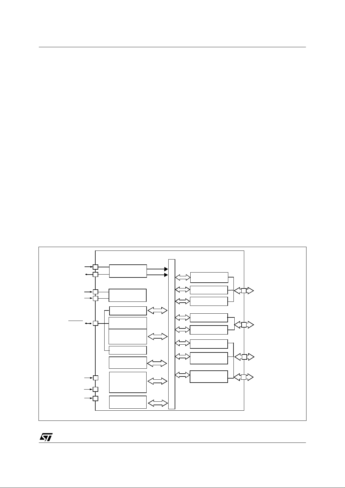
Figure 1. General Block Diagram
Internal
CLOCK
OSCIN
OSCOUT
V
V
RESET
DD
SS
OSCILLATOR
POWER
SUPPLY
WATCHDOG
CONTROL
8-BIT CO RE
ALU
LVD
USB DMA
OSC/3
OSC/4 or OSC/2
(for USB)
– industry standard asynchronous SCI serial inter-
face (not on all products - see device summary
below)
– digital Watchdog
– 16-bit Timer featuring an External clock input, 2
Input Captures, 2 Output Compares with Pulse
Generator capabilit ies
– fast I2C Multi Master interface (not on all prod-
ucts - see device summary)
– Low voltage (LVD) reset ensuring proper power-
on or power-off of the device
All ST7263 MCUs are available in ROM and OTP
versions.
The ST72E631 is the EPROM version of the
ST7263 in CSDIP32 windowed packages.
A specific mode is available to allow programming
of the EPROM user memory array. This is set by a
specific voltage source applied to the V
PP
pin.
I2C*
PORT A
16-BI TTIMER
ADDRESS AND DATA BUS
PORT B
ADC
PORT C
SCI*
(UART)
PA[7:0]
(8 bits)
PB[7:0]
(8 bits)
PC[2:0]
(3 bits)
/TEST
VPP/TEST
V
DDA
V
SSA
* not on all products ( ref er to Table 1: Device Summary)
PROGRAM
MEMORY
(4K/8K/16K Byte s)
RAM
(256/512 Bytes)
USB SIE
USBDP
USBDM
USBVCC
5/109
ST7263
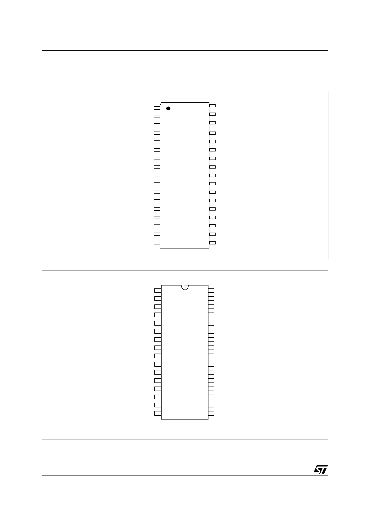
1.2 PIN DESCRI PTION
Figure 2. 34-Pin SO Package Pinout
OSCOUT
OSCIN
PC2/USBOE
PC1/TDO
PC0/RDI
RESET
AIN7/IT8/PB7
AIN6/IT7/PB6
AIN5/IT6/PB5
AIN4/IT5/PB4
* V
on EPROM/OTP versions only
PP
AIN3/PB3
AIN2/PB2
AIN1/PB1
(10mA)
(10mA)
VPP/TEST
(10mA)
(10mA)
(10mA)
(10mA)
(10mA)
V
V
DD
SS
NC
1
2
3
4
5
6
7
8
9
10
11
12
13
14
15
16
17
V
34
DDA
USBVCC
33
USBDM
32
USBDP
31
V
30
SSA
PA0/MCO
29
PA1
28
NC
27
NC
26
NC
25
PA2
24
23
PA3/EXTCLK
22
PA4/ICAP1/IT1
PA5/ICAP2/IT2
21
PA6/OCMP1/IT3
20
PA7/OCMP2/IT4
19
PB0
18
(25mA)
(25mA)
(10mA)
/SDA
/SCL
/AIN0
Figure 3. 32-Pin SDIP Package Pinout
V
DD
OSCOUT
OSCIN
V
SS
PC2/USBOE
PC1/TDO
PC0/RDI
RESET
AIN7/IT8/PB7
AIN6/IT7/PB6
AIN5/IT6/PB5
AIN4/IT5/PB4
* V
on EPROM/OTP versions only
PP
AIN3/PB3
AIN2/PB2
AIN1/PB1/
(10mA)
(10mA)
VPP/TEST*
(10mA)
(10mA)
(10mA)
(10mA)
(10mA)
10
11
12
13
14
15
16
1
2
3
4
5
6
7
8
9
V
32
USBVCC
31
USBDM
30
USBDP
29
V
28
PA0/MCO
27
PA1
26
25
24
PA2
23
PA3/EXTCLK
22
21
PA4/ICAP1/IT1
PA5/ICAP2/IT2
20
PA6/COMP1/IT3
19
PA7/COMP2/IT4
18
PB0
17
DDA
NC
NC
SSA
(25mA)
(25mA)
(10mA)
/SDA
/SCL
/AIN0
6/109
PIN DESCRIPTION (Cont’d)
RESET
(see Note 1): Bidirectional. This active low
signal forces the initialization of the MCU. This
event is the top priority non maskable interrupt.
This pin is switched low when the Watchdog has
triggered or V
is low. It can be used to reset ex-
DD
ternal peripherals.
OSCIN/OSCOUT: Input/Output Oscillator pin.
These pins connect a pa rallel-resonant crystal, or
an external sou rc e to the on -c h ip o s cilla t o r.
V
/TEST: EPROM programming input. This pin
PP
must be held low during normal operating modes.
V
DD/VSS
(see Note 2): Main power supply and
Ground voltages.
V
DDA/VSSA
(see Note 2): Power Supply and
Ground for analog peripherals.
Table 2. Device Pin Description
ST7263
Alter na te Fu nct i ons : Several pins of the I/O ports
assume software programmable alternate functions as shown in the pin description.
Note 1: Adding t wo 100nF de coupling capa citors
V
together
DD
DD
and
on Reset pin (respectively connected to
V
) will significantly improve produc t electromag-
SS
netic susceptibility performances.
Note 2: To enhance reliability of operation, it is
recommended to conn ect
V
DDA
and V
on the application board. The same recommenda-
V
tions apply to
and VSS.
SSA
Pin n°
Pin Name
SO34
SDIP32
11V
2 2 OSCOUT O Oscillator output
3 3 OSCIN I Oscillator input
44V
5 5 PC2/USBOE I/O C
6 6 PC1/TDO I/O C
7 7 PC0/RDI I/O C
8 8 RESET I/O X X Reset
-- 9 NC -- Not connected
9 10 PB7/AIN7/IT8 I/O C
10 11 PB6/AIN6/IT7 I/O C
11 12 V
12 13 PB5/AIN5/IT6 I/O C
13 14 PB4/AIN4/IT5 I/O C
14 15 PB3/AIN3 I/O C
15 16 PB2/AIN2 I/O C
16 17 PB1/AIN1 I/O C
17 18 PB0/AIN0 I/O C
18 19 PA7/OCMP2/IT4 I/O C
19 20 PA6/OCMP1/IT3 I/O C
DD
SS
/TEST S Supply for EPROM and test input
PP
Level Port / Control
Input Output
Type
Input
Output
float
S Power supply voltage (4V - 5.5V)
S Digital ground
T
T
T
10mA X XX XPort B7 ADC analog input 7
T
10mA X XX XPort B6 ADC analog input 6
T
10mA X XX XPort B5 ADC analog input 5
T
10mA X XX XPort B4 ADC analog input 4
T
10mA X XXPort B3 ADC analog input 3
T
10mA X XXPort B2 ADC analog input 2
T
10mA X XXPort B1 ADC analog input 1
T
10mA X XXPort B0 ADC Analog Input 0
T
T
T
int
wpu
X X Port C2 USB Output Enable
X X Port C1 SCI transmit data output
X X Port C0 SCI Receive Data Input
X XXPort A7 Timer Output Compare 2
X XXPort A6 Timer Output Compare 1
OD
ana
Main
Function
(after reset)
PP
Alternate Function
*)
*)
7/109
ST7263
Pin n°
Pin Name
SO34
SDIP32
20 21 PA5/ICAP2/IT2 I/O C
21 22 PA4/ICAP 1/IT1 I/O C
22 23 PA3/EXTC LK I/O C
23 24 PA2/SCL I/O C
-- 25 NC -- Not connected
24 26 NC -- Not connected
25 27 NC -- Not connected
26 28 PA1/SDA I/O C
27 29 PA0/MCO I/O C
28 30 V
29 31 USBDP I/O USB bidirectional data (data +)
30 32 USBDM I/O USB bidirectional data (data -)
31 33 USBVCC O USB power supply
32 34 V
SSA
DDA
Level Port / Control
Input Output
Type
Input
Output
float
T
T
T
25mA X T Port A2 I2C serial clock
T
25mA X T Port A1 I2C serial data
T
T
S Analog ground
S Analog supply voltage
int
wpu
X XXPort A5 Timer Input Captu re 2
X XXPort A4 Timer Input Captu re 1
X X Port A3 Timer External Clock
XXPort A0 Main Clock Output
OD
ana
Main
Function
(after reset)
PP
Alternate Function
*)
*)
*: if the peripheral is present on the device (see Table 1 Device Summary)
Legend / Abbreviations for Figure 2 and Tab le 2:
Type: I = input, O = output, S = supply
In/Output lev e l: C
= CMOS 0.3VDD/0.7VDD with input trigger
T
Output level: 10mA = 10mA high sink (on N-buffer only)
25mA = 25mA very high sink (on N-buffer only)
Port and control configuration:
– Input: float = floating, wpu = weak pull-up, int = interrupt, ana = analog
– Output : OD = open drain, PP = push-pull, T = True open drain
Refer to “I/O PORTS” on page 25 for more details on the software configuration of the I/O ports.
The RESET configuration of each pin is shown in bold. This configuration is kept as long as the device is
under reset state.
8/109
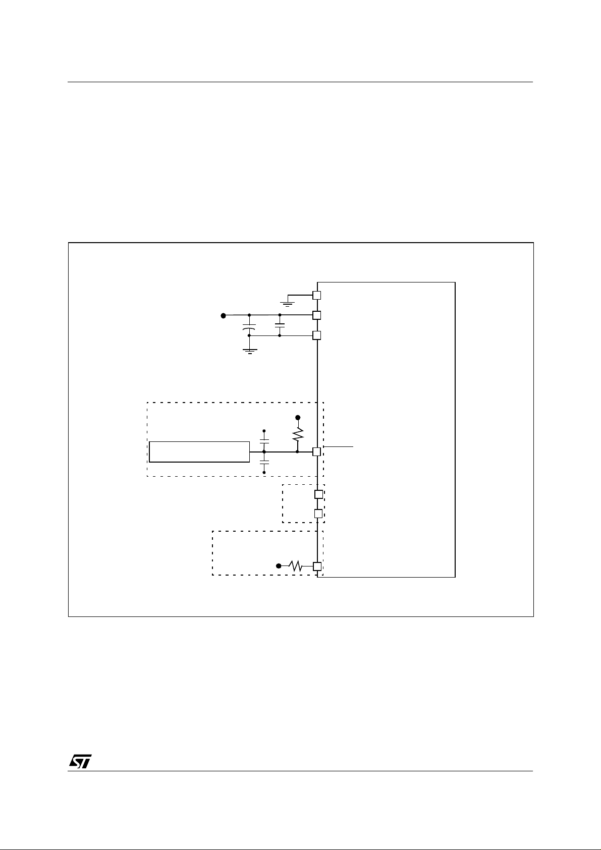
1.3 EXTERNAL CONNECTIONS
ST7263
The following figure shows the recom mended external connections for the device.
The V
pin is only used for programming OTP
PP
and EPROM devices and must be tied to ground in
user mode.
The 10 nF and 0. 1 µF decoupling capacitors on
the power supply lines are a suggested EMC performance/cost tradeoff.
Figure 4. Recommended Extern al Connec tions
V
DD
Optional if Low Voltage
Detector (LVD) is used
EXTERNAL RESET CIRCUIT
10nF
+
V
DD
0.1µF
0.1µF
The external reset network is intended to protect
the device against parasitic resets, especially in
noisy environments.
Unused I/Os shoul d be t ied hi gh to av oid any unnecessary power consumption on floating lines.
An alternative solution is to program the unused
ports as inputs with pull-up.
V
PP
V
4.7K
DD
V
SS
RESET
0.1µF
See
Clocks
Section
Or configure unused I/O ports
by software as input with pull-up
V
10K
DD
OSCIN
OSCOUT
Unused I/O
9/109
ST7263
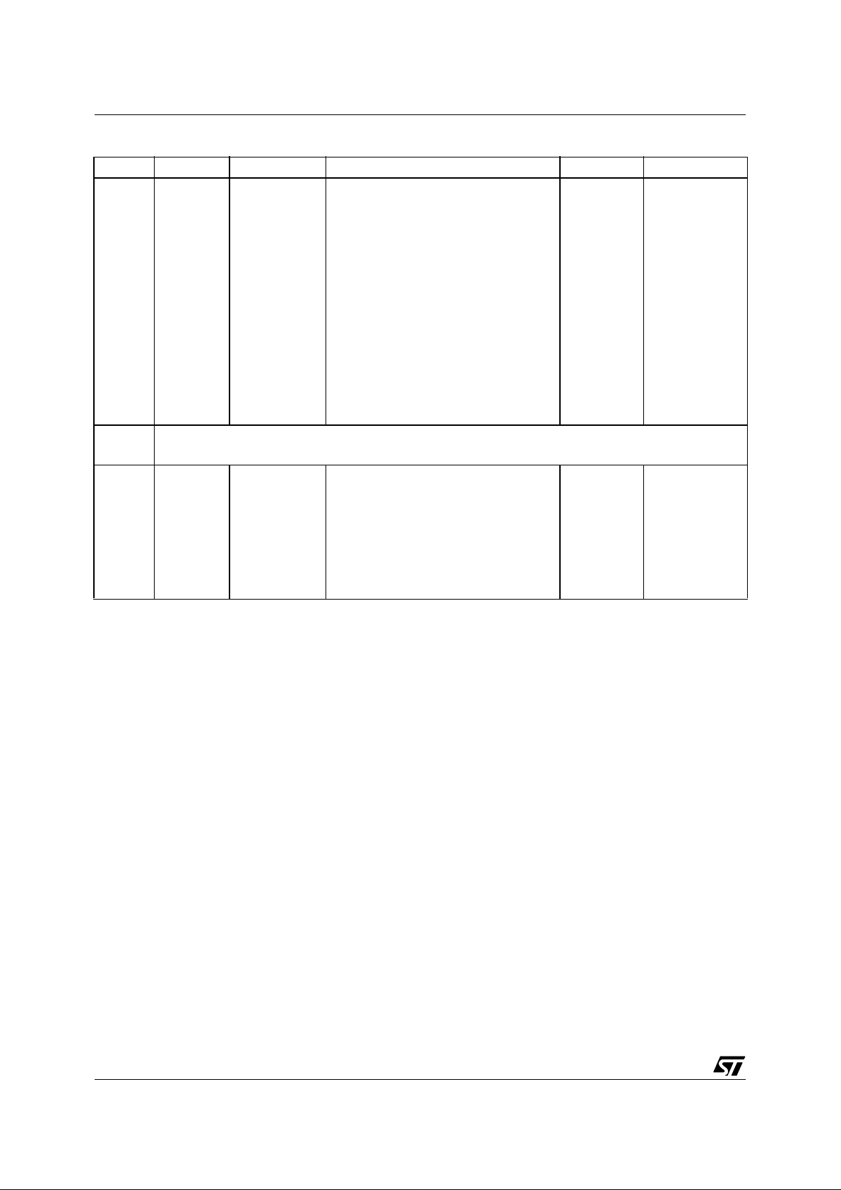
1.4 REGISTER & MEMORY MAP
As sho wn in Figure 5, the MCU is capable of ad-
dressing 64K bytes of memories and I/O registers.
The available memory locations consist of 192
bytes of register location, up to 512 bytes of RAM
and up to 16K bytes of user program memory. The
RAM space includes up to 64 bytes for the stack
from 0100h to 013Fh.
Figure 5. Me m ory Map
0000h
003Fh
0040h
023Fh
0240h
BFFFh
C000h
E000h
F000h
FFEFh
FFF0h
FFFFh
HW Registers
(see Table 4
256 Bytes RAM*
512 Bytes RAM*
Reserved
Program Memory*
16K Bytes
8K Bytes
4K Bytes
Interrupt & Reset Vectors
(see Table 3 on page 10)
The highest address by tes contain the user re set
and interrupt vectors.
IMPORTANT: Memory locations noted “Reserved” must neve r be ac cess ed. A cce ssing a reserved area can have unpredictable effects on the
device
0040h
00FFh
0100h
013Fh
0040h
00FFh
0100h
013Fh
0140h
023Fh
Short Addressing
RAM (192 Bytes)
Stack (64 Bytes)
Short Addressing
RAM (192 Bytes)
Stack (64 Bytes)
16-bit Addressing RAM
(256 Bytes)
* Program memory and RAM sizes are product dependent (see Table 1 Device Summary)
Table 3. Interrupt Vector Map
Vector Address Description Masked by Remarks Exit from Halt Mode
FFF0-FFF1h
FFF2-FFF3h
FFF4-FFF5h
FFF6-FFF7h
FFF8-FFF9h
FFFA-FFFBh
FFFC-FFFDh
FFFE-FFFFh
USB End Suspend Mode Interrupt Vector
USB Interrupt Vector
SCI Interrupt Vector*
2
C Interrupt Vector*
I
TIMER Interrupt Vector
IT1 to IT8 Interrupt Vector
TRAP (software) Interrupt Vector
RESET Vector
I- bit
I- bit
I- bit
I- bit
I- bit
I- bit
none
none
Internal Interrupt
Internal Interrupt
Internal Interrupt
Internal Interrupt
External Interrupts
Internal Interrupt
CPU Interrupt
No
No
No
No
Yes
Yes
No
Yes
* If the peripheral is present on the device (see Table 1 Device Summary)
10/109
ST7263
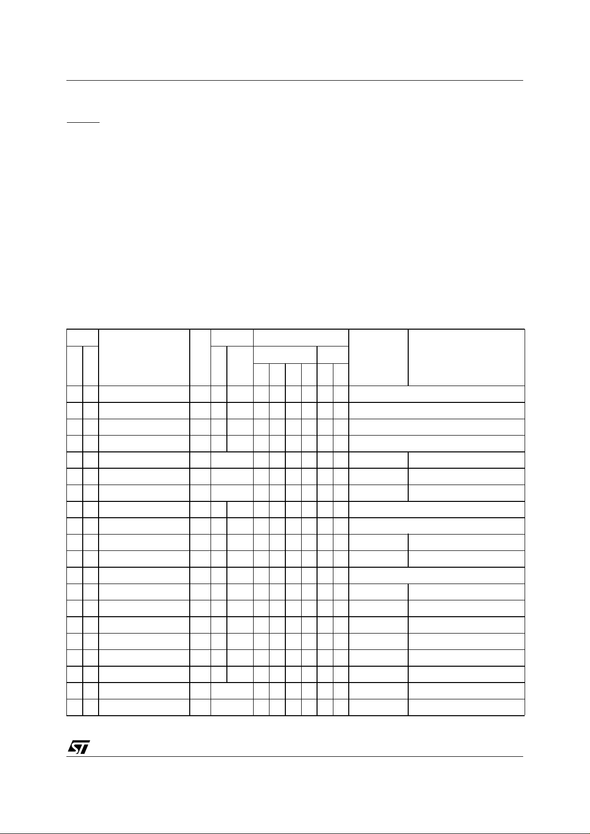
Table 4. Hardware Register Memory Map
Address Block Register Label Register name Reset Status Remarks
0000h
0001h
0002h
0003h
0004h
0005h
0006h
0007h
0008h ITIFRE Interrupt Register 00h R/W
0009h MISCR Miscellaneous Register F0h R/W
000Ah
000Bh
000Ch WDG CR Watchdog Control Register 7Fh R/W
000Dh
0010h
0011h
0012h
0013h
0014h
0015h
0016h
0017h
0018h
0019h
001Ah
001Bh
001Ch
001Dh
001Eh
001Fh
0020h
0021h
0022h
0023h
0024h
ADC
TIM
SCI
1)
PADR
PADDR
PBDR
PBDDR
PCDR
PCDDR
DR
CSR
CR2
CR1
SR
IC1HR
IC1LR
OC1HR
OC1LR
CHR
CLR
ACHR
ACLR
IC2HR
IC2LR
OC2HR
OC2LR
SR
DR
BRR
CR1
CR2
Port A Data Register
Port A Data Direction Register
Port B Data Register
Port B Data Direction Register
Port C Data Register
Port C Data Direction Register
Reserved (2 Bytes)
ADC Data Register
ADC control Status register
Reserved (4 Bytes)
Timer Control Register 2
Timer Control Register 1
Timer Status Register
Timer Input Capture High Register 1
Timer Input Capture Low Register 1
Timer Output Compare High Register 1
Timer Output Compare Low Register 1
Timer Counter High Register
Timer Counter Low Register
Timer Alternate Counter High Register
Timer Alternate Counter Low Register
Timer Input Capture High Register 2
Timer Input Capture Low Register 2
Timer Output Compare High Register 2
Timer Output Compare Low Register 2
SCI Status Register
SCI Data Register
SCI Baud Rate Register
SCI Control Register 1
SCI Control Register 2
00h
00h
00h
00h
1111 x000b
1111 x000b
00h
00h
00h
00h
00h
xxh
xxh
80h
00h
FFh
FCh
FFh
FCh
xxh
xxh
80h
00h
C0h
xxh
00xx xxxxb
xxh
00h
R/W
R/W
R/W
R/W
R/W
R/W
Read only
R/W
R/W
R/W
Read only
Read only
Read only
R/W
R/W
Read only
R/W
Read only
R/W
Read only
Read only
R/W
R/W
Read only
R/W
R/W
R/W
R/W
11/109
ST7263
Address Block Register Label Register name Reset Status Remarks
0025h
0026h
0027h
0028h
0029h
002Ah
002Bh
002Ch
002Dh
002Eh
002Fh
0030h
0031h
0032h
0038h
0039h
003Ah
003Bh
003Ch
003Dh
003Eh
003Fh
USB
2C1)
I
PIDR
DMAR
IDR
ISTR
IMR
CTLR
DADDR
EP0RA
EP0RB
EP1RA
EP1RB
EP2RA
EP2RB
DR
OAR
CCR
SR2
SR1
CR
USB PID Register
USB DMA address Register
USB Interrupt/DMA Register
USB Interrupt Status Register
USB Interrupt Mask Register
USB Control Register
USB Device Address Register
USB Endpoint 0 Register A
USB Endpoint 0 Register B
USB Endpoint 1 Register A
USB Endpoint 1 Register B
USB Endpoint 2 Register A
USB Endpoint 2 Register B
Reserved (7 Bytes)
2
C Data Register
I
Reserved
I2C (7 Bits) Slave Address Register
2
C Clock Control Register
I
2
C 2nd Status Register
I
2
C 1st Status Register
I
2
C Control Register
I
xxh
xxh
xxh
00h
00h
xxxx 0110b
00h
0000 xxxxb
80h
0000 xxxxb
0000 xxxxb
0000 xxxxb
0000 xxxxb
00h
00h
00h
00h
00h
00h
Read only
R/W
R/W
R/W
R/W
R/W
R/W
R/W
R/W
R/W
R/W
R/W
R/W
R/W
R/W
R/W
Read only
Read only
R/W
Note 1. If the peripheral is present on the device (see Table 1 Device Summary)
12/109

1.5 EPROM/OTP PROGRAM MEMORY
ST7263
The program memory of the ST72T63 may be programmed using the EPR OM program m ing b oards
available from STMicroelectronics (see Table 26).
1.5.1 EPROM ERASURE
ST72Exxx EPROM devices are erased by exposure to high intensity UV light admitted through the
transparent window. This exposure discharges the
floating gate to its initial state through induced
photo current.
It is recommended that the ST72Exxx devices be
kept out of direct sunlight, since the UV content of
sunlight can be sufficient to cause functional failure. Extended exposure t o room level fluorescent
lighting may also cause erasure.
An opaque coating (paint, tape, label, etc...)
should be placed over the package window if the
product is to be operated under these lighting conditions. Covering the window also reduces I
DD
in
power-saving modes du e to photo-diode leakage
currents.
An Ultraviolet source of wave length 2537 Å yielding a total integrated dosage of 15 Watt-sec/cm
2
is
required to erase the ST72Exxx. The device will
be erased in 15 to 30 minutes if such a UV lamp
with a 12mW/cm
2
power rating is placed 1 inch
from the device window without any interposed filters.
13/109
ST7263
2 CENTRAL PROCE SSI NG UNIT
2.1 INTRODUCTION
This CPU has a full 8-bit architecture and contains
six internal registers allowing efficient 8-bit data
manipulation.
2.2 MAIN FEATURES
■ 63 basic instructions
■ Fast 8-bit by 8-bit multiply
■ 17 main addressing modes
■ Two 8-bit index registers
■ 16-bit stack pointer
■ Low po wer modes
■ Maskable hardware interrupts
■ Non-maskable software interrupt
2.3 CPU REGISTERS
The 6 CPU registers shown in Figure 1 are not
present in the memory mapping and are accessed
by specific instructions.
Figure 6. CPU Registers
70
RESET VALUE = XXh
70
RESET VALUE = XXh
70
RESET VALUE = XXh
Accumulator (A)
The Accumulator is an 8-bit general purpose register used to hold operan ds and the results of the
arithmetic and logic calculations and to manipulate
data.
Index Registers (X and Y)
In indexed addressing modes, these 8-bit registers
are used to create either effective addresses or
temporary storage areas for data manipulation.
(The Cross-Assembler generates a precede instruction (PRE) to indicate that the following instruction refers to the Y register.)
The Y register is not affected by the interrupt automatic procedures (not pushed to and popped from
the stack).
Program Cou nt er (P C )
The program counter is a 16-bit register containing
the address of the next instruction to be executed
by the CPU. It is made of two 8-bit registers PCL
(Program Counter Low which is the LSB) and PCH
(Program Counter High which is the MSB).
ACCUMULA T OR
X INDEX REGISTER
Y INDEX REGISTER
15 8
RESET VALUE = RESET VECTOR @ FFFEh-FFFFh
15
RESET VALUE = STACK HIGHER ADDRESS
14/109
PCH
RESET VALUE =
7
70
1C11HI NZ
1X11X1XX
70
8
PCL
0
PROGRAM COUNTER
CONDITION CODE REGISTER
STACK POINTER
X = Undefined Value

CPU REGISTERS (Cont’d)
CONDITION CODE REGISTER (CC)
Read/Write
Reset Value: 111x1xxx
70
111HINZC
The 8-bit Condition Code register c ontains the interrupt mask and four flags represent ative of the
result of the instruction just executed. This register
can also be handled by the PUSH and POP instructions.
These bits can be individually tested and/or controlled by specific instructions.
because the I bi t is set by hardware at the start of
the routine and reset by the IRET instruction at the
end of the routine. If the I bit is cleared by software
in the interrupt routine, pending interrupts are
serviced regardless of the priority level of the current interrupt routine.
Bit 2 = N
Negative
.
This bit is set and cleared by hardware. It is representative of the result sign of the last arithmeti c,
logical or data manipulation. It is a copy of the 7
bit of the result.
0: The result of the last operation is positive or null.
1: The result of the last operation is negative
(i.e. the most significant bit is a logic 1).
This bit is accessed by the JRMI and JRPL instruc-
Bit 4 = H
Half carry
.
tions.
This bit is set by hardware when a carry occurs between bits 3 and 4 of t he ALU during an ADD or
ADC instruction. It is reset by hardware during the
same instructions.
0: No half carry has occurred.
1: A half carry has occurred.
This bit is tested using the JRH or JRNH instruction. The H bit is useful in BCD arithmetic subroutines .
Bit 1 = Z
This bit is set and cleared by hardware. This bit in-
dicates that the result of the last arithmetic, logical
or data manipulation is zero.
0: The result of the last operation is different from
zero.
1: The result of the last operation is zero.
Zero
.
This bit is accessed by the JREQ and JRNE test
instructions.
Bit 3 = I
Interrupt mask
This bit is set by hardware when entering in interrupt or by software to disable all interrup ts except
the TRAP software interrupt. This bit is cleared by
software.
0: Interrupts are enabled.
1: Interrupts are disabled.
This bit is controlled by the RIM, SIM and IRET instructions and is tested by the JRM and JRNM instructions.
Note: Interrupts requested while I is set are
latched and can be processed whe n I is cleared.
.
Bit 0 = C
Carry/borrow.
This bit is set and cleared b y hardware and software. It indicates an overflow or an underflow has
occurred during the last arithmetic operation.
0: No overflow or underflow has occurred.
1: An overflow or underflow has occurred.
This bit is driven by the SCF and RCF instructions
and tested by the JRC and JRNC instructions. It is
also affected by the “bit test and branch”, shift and
rotate instructions.
By default an interrupt routine is not in terruptable
ST7263
th
15/109
ST7263
CPU REGISTERS (Cont’d)
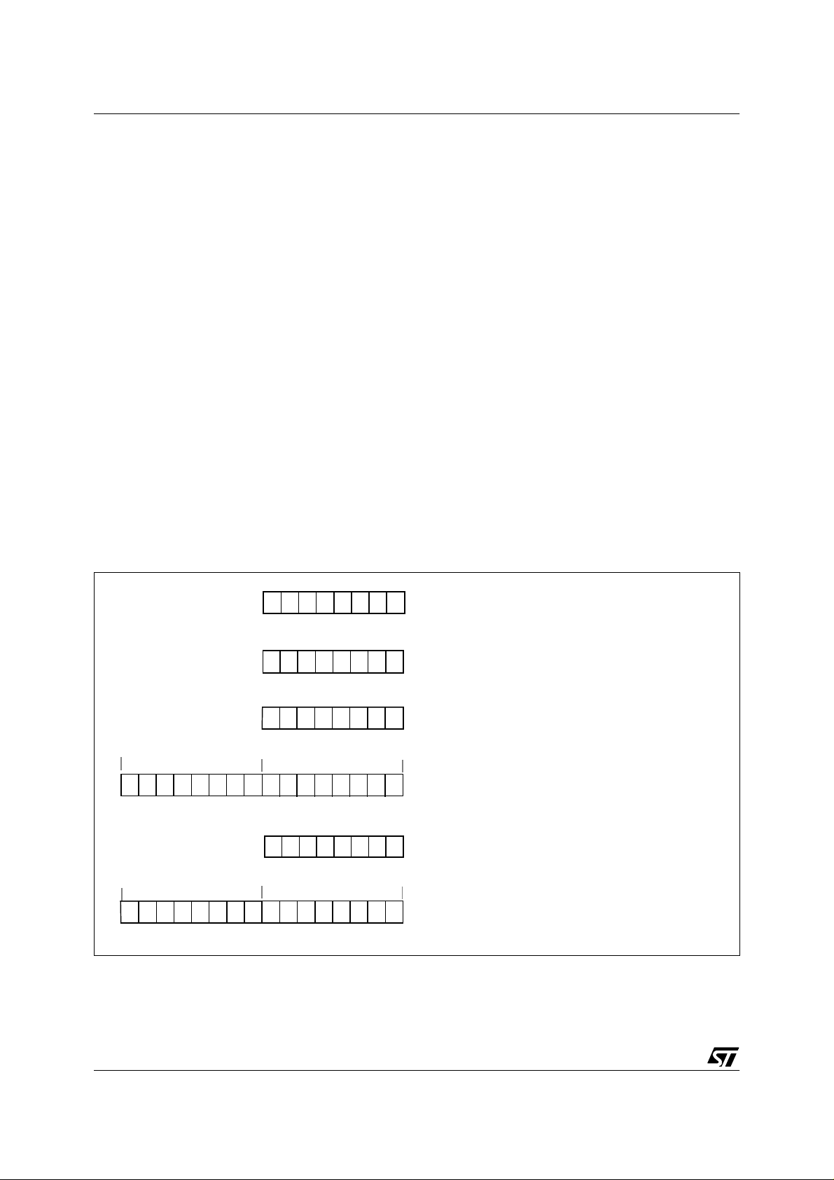
Stack Pointer (SP)
Read/Write
Reset Value: 01 3Fh
15 8
00000001
70
0 0 SP5 SP4 SP3 SP2 SP1
SP0
The Stack Pointer is a 16-bit register which is always pointing to the next free location in the stack.
It is then decremented after data has been pushed
onto the stack and incremented before data is
popped from the stack (see Figure 7).
Since the stack is 64 bytes deep, the 10 most significant bits are forced by hardw are. Following a n
MCU Reset, or after a Reset Stack Pointe r instruction (RSP), the Stack Pointer contains its reset value (SP5 to SP0 bits are set) which is the stack
higher address.
The least significant byte of the Stack Pointer
(called S) can be directly accessed by a LD instruction.
Note: When the lower limit is exceeded, the Stack
Pointer wraps around to the stack upper limit, wi thout indicating the s tack overflow. The previously
stored information is then o verwritten and therefore lost. The stack also wraps in case of an underflow.
The stack is used to save the retu rn address during a subroutine call and the CPU context during
an interrupt. The user may also directly manipulate
the stack by means of the PUSH and POP instructions. In the case of an interrupt, the PCL is stored
at the first location point ed to by the SP. Then the
other registers are stored in the next locations as
shown in Figure 7.
– When an interrupt is received, the SP is decre-
mented and the context is pushed on the stack.
– On return from interrupt, the SP is incremented
and the context is popped from the stack.
A subroutine call occupies two locations and an interrupt five locat ions i n the sta ck ar ea.
Figure 7. Stack Manipulation Example
@ 0100h
SP
@ 013Fh
CALL
Subroutine
SP
PCH
PCL
Stack Higher Address = 013Fh
Stack Lower Address =
Interrupt
Event
SP
CC
A
X
PCH
PCL
PCH
PCL
0100h
PUSH Y POP Y IRET
SP
Y
CC
A
X
PCH
PCL
PCH
PCL
CC
A
X
PCH
PCL
PCH
PCL
SP
PCH
PCL
RET
or RSP
SP
16/109
3 CLOCKS AND RESET
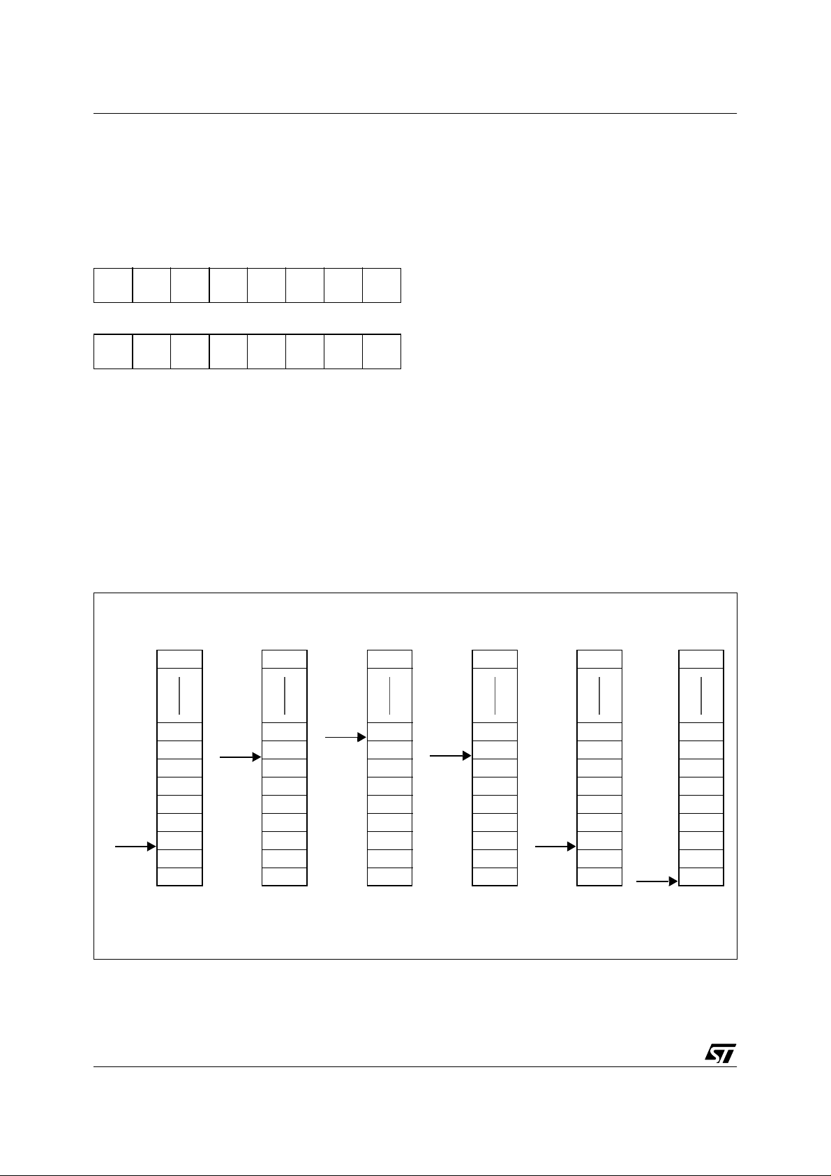
3.1 CLOCK SYSTEM
ST7263
3.1.1 General Description
The MCU accepts either a Crystal or Ceramic resonator, or an external clock signal to drive the internal oscillator. The internal clock (f
rived from the external oscillator frequency (f
CPU
) is de-
OSC
which is divided by 3 (and by 2 or 4 for USB, depending on the external clock used).
By setting the CLKDIV bit in the Miscellaneous
Register, a 12 MHz external clock can be used giving an internal frequency of 4 MHz while maintaining a 6 MHz for USB (refer to Figure 10).
The internal clock signal (f
) is also routed to
CPU
the on-chip peripherals. The CPU clock signal
consists of a square wave with a duty cycle of
50%.
The internal oscillat or is designed to operate with
an AT-cut parallel resonant quartz or ceramic resonator in the frequency range specified for f
osc
The circuit shown in Figure 9 is recommended
when using a crystal, and Table 5 Re commended
Values for 24 MHz Crystal Resonator lists the rec-
ommended capacitance. The crystal and associated components should be mounted as close as
possible to the input pins in order to minimize output distortion and start-up stabilisation time.
Figure 8. External Clock Source Connections
),
OSCIN OSCOUT
NC
EXTERNAL
CLOCK
Figure 9. Crystal/Ceramic Resonator
.
OSCOUT
R
P
C
OSCOUT
C
OSCIN
OSCIN
Table 5. Recommended Values for 24 MHz
Crystal Resonator
R
SMAX
C
OSCIN
C
OSCOUT
R
P
Note: R
crystal (see crystal specification).
SMAX
20
Ω
56pF 47pF 22pF
56pF 47pF 22pF
1-10 M
Ω
25
1-10 M
Ω
Ω
70
1-10 M
Ω
Ω
is the equivalent serial resistor of the
3.1.2 External Clock
An external clock may be applied to the OSCIN input with the OSCOUT pin not connected, as
shown on F igure 8. The t
specifications does
OXOV
not apply when using an external clock input. The
equivalent specification of the external clock
source should be used instead of t
OXOV
(see Sec-
tion 6.5 CONTROL TIMING).
Figure 10. Clock block diagram
%3
CLKDIV
1
%2
24 or
12 MHz
Crystal
%2
0
%2
8 or 4 MHz
CPU and
peripherals)
6 MHz (USB)
17/109
ST7263
3.2 RESET
The Reset procedure is used to provide an orderly
software start-up or to exit low power modes.
Three reset modes are provided: a low voltage
(LVD) reset, a watchdog reset and an external reset at the RESET
pin.
A reset causes the reset vector to be fetched from
addresses FFFEh and FFFFh in order to be loaded
into the PC and with program execution starting
from this point.
An internal circuitry provides a 4096 CPU clock cycle delay from the time that the oscillator becomes
During low voltage reset, the RESET
thus permitting the MCU to reset other devices.
The Low Voltage Detector can be disabled by setting the LVD bit of the Miscellaneous Register.
3.2.2 Watchdog Reset
When a watchdog reset occurs, the RESET
pulled low permitting the MCU to reset other devices in the same way as t he low voltage reset (Fig-
ure 11).
pin is held low,
pin is
active.
3.2.3 External Reset
3.2.1 Low Voltage Detector (LVD)
Low voltage reset circuitry generates a reset when
V
is:
DD
■ below V
■ below V
when VDD is rising,
IT+
when VDD is falling.
IT-
The external reset is an active low input signal applied to the RESET pin of the MCU.
As shown in Figure 14, the RESET
signal must
stay low for a minimum of one and a half CPU
clock cycles.
An internal Schmitt trigger at the RESET
pin is pro-
vided to improve noise immunity.
Table 6. List of secti ons affect ed by RESET, WA IT and HAL T (Ref er t o 3.5 for Wait a nd Hal t Modes )
Section RESET WAIT HALT
CPU clock running at 8 MHz X
Timer Prescaler reset to zero X
Timer Counter set to FFFCh X
All Timer enable bit set to 0 (disable) X
Data Direction Registers set to 0 (as Inputs) X
Set Stack Pointer to 013Fh X
Force Internal Address Bus to restart vector FFFEh,FFFFh X
Set Interrupt Mask Bit (I-Bit, CCR) to 1 (Interrupt Disable) X
Set Interrupt Mask Bit (I-Bit, CCR) to 0 (Interrupt Enable) X X
Reset HALT latch X
Reset WAIT latch X
Disable Oscillator (for 4096 cycles) X X
Set Timer Clock to 0 X X
Watchdog counter reset X
Watchdog register reset X
Port data registers reset X
Other on-chip peripherals: registers reset X
18/109
ST7263
Figure 11. Low Voltage Detector functional Diagram
RESET
V
DD
LOW VOLTAGE
DETECTOR
FROM
WATCHDOG
RESET
INTERNAL
RESET
Figure 12. Low Voltage Reset Signal Output
V
IT+
V
DD
RESET
Note: Hysteresis (V
Figure 13. Temporization timing diagram after an internal Reset
V
V
DD
Addresses
IT+
temporization (4096 CPU clock cycles)
$FFFE
IT+-VIT-
) = V
hys
V
IT-
Figure 14. Reset Timing Diagram
t
DDR
V
DD
OSCIN
t
OXOV
f
CPU
PC
RESET
WATCHDOG RESET
Note: Refer to Electrical Characteristics for values of t
4096 CPU
CLOCK
CYCLES
, t
DDR
DELAY
OXOV
FFFE
, V
IT+
, V
FFFF
IT-
and V
hys
19/109

ST7263
4 INTERRUPTS AND POWER SAVING MODES
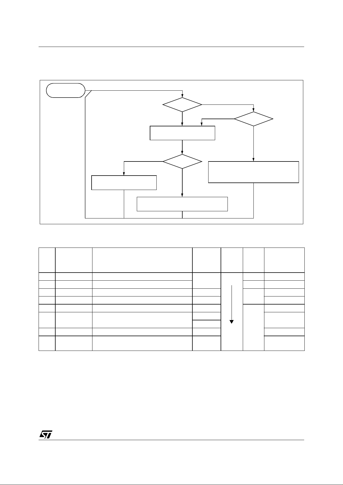
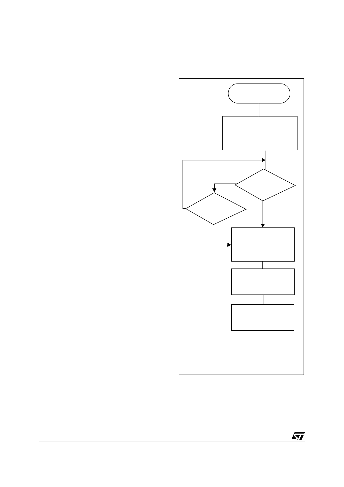
4.1 INTERRUPTS
The ST7 core may be interrupted by one of two different methods: maskable hardware interrupts as
listed in Table 7 Interrupt Mapping and a non-
maskable software interrupt (TRAP). The Interrupt
processing flowchart is shown in Figure 15.
The maskable interrupts must be enabled clearing
the I bit in order to be serviced. However, disabled
interrupts may be latched and processed when
they are enabled (see external interrupts subsec tion) .
When an interrupt has to be serviced:
– Normal processing is suspended at the end of
the current instruction execution.
– The PC, X, A and CC registers are saved onto
the stack.
– The I bit of the CC register is set to prevent addi-
tional interrupts.
– The PC is then loaded with the interrupt vector of
the interrupt to service and the first instruction of
the interrupt service routine is fetched (refer to
Table 7 Interrupt Mapping for vector addresses).
The interrupt service routine should finish with the
IRET instruction which c auses the conten ts o f the
saved registers to be recovered from the stack.
Note: As a consequence of the IRET instruction,
the I bit will be cleared a nd the main pro gram will
resume.
Priority management
By default, a servicing interrupt can not be interrupted because the I bit is set by hardware entering in interrupt routine.
In the case several interrupts are simultaneously
pending, a hardware priority defines which one will
be serviced first (see Table 7 Interrupt Mapping).
Non maskable software interrupts
This interrupt is entered when the TRAP instruction is executed regardless of the state of the I bit.
It will be serviced according to the flowchart on
Figure 15.
Interrupts a n d Low power mod e
All interrupts allow the processor to leave the Wait
low power mode. Only external and specific mentioned interrupts allow the processor to leave the
Halt low power mode (refer to t he “Exit f rom HALT“
column in Table 7 Interrupt Mapping).
External interrupts
The pins ITi/PAk and ITj/P Bk (i=1,2; j= 5,6; k=4,5)
can generate an i nterrupt when a rising edge occurs on this pin. Conversely, pins ITl/PAn and ITm/
PBn (l=3,4; m= 7,8; n=6,7) can generat e an interrupt when a falling edge occurs on this pin.
Interrupt generation will occur if it is enabl ed with
the ITiE bit (i=1 to 8) in the ITRFRE register and if
the I bit of the CCR is reset.
Peripheral interrupts
Different peripheral interrupt flags in the status
register are able to cause an interrupt when they
are active if both.
– The I bit of the CC register is cleared.
– The corresponding enable bit is set in the control
register.
If any of these two conditions is false, the interrupt
is latched and thus remains pending.
Clearing an interrupt request is done by:
– writing “0” to the corresponding bit in the status
register or
– an access to the status register while the flag is
set followed by a read or write of an associated
register.
Notes:
1. The clearing sequence resets the internal latch.
A pending interrupt (i.e. waiting for being enabled)
will therefore be lost if the clear sequence is executed.
2. All interrupts allow the processor to leave the
Wait low power mode.
3. Exit from Halt mode may only be triggered by an
External Interrupt on one of the ITi ports (PA4-PA7
and PB4-PB7), an end suspend mode Interrupt
coming from USB peripheral, or a reset.
20/109
INTERRUPTS (Cont’d)
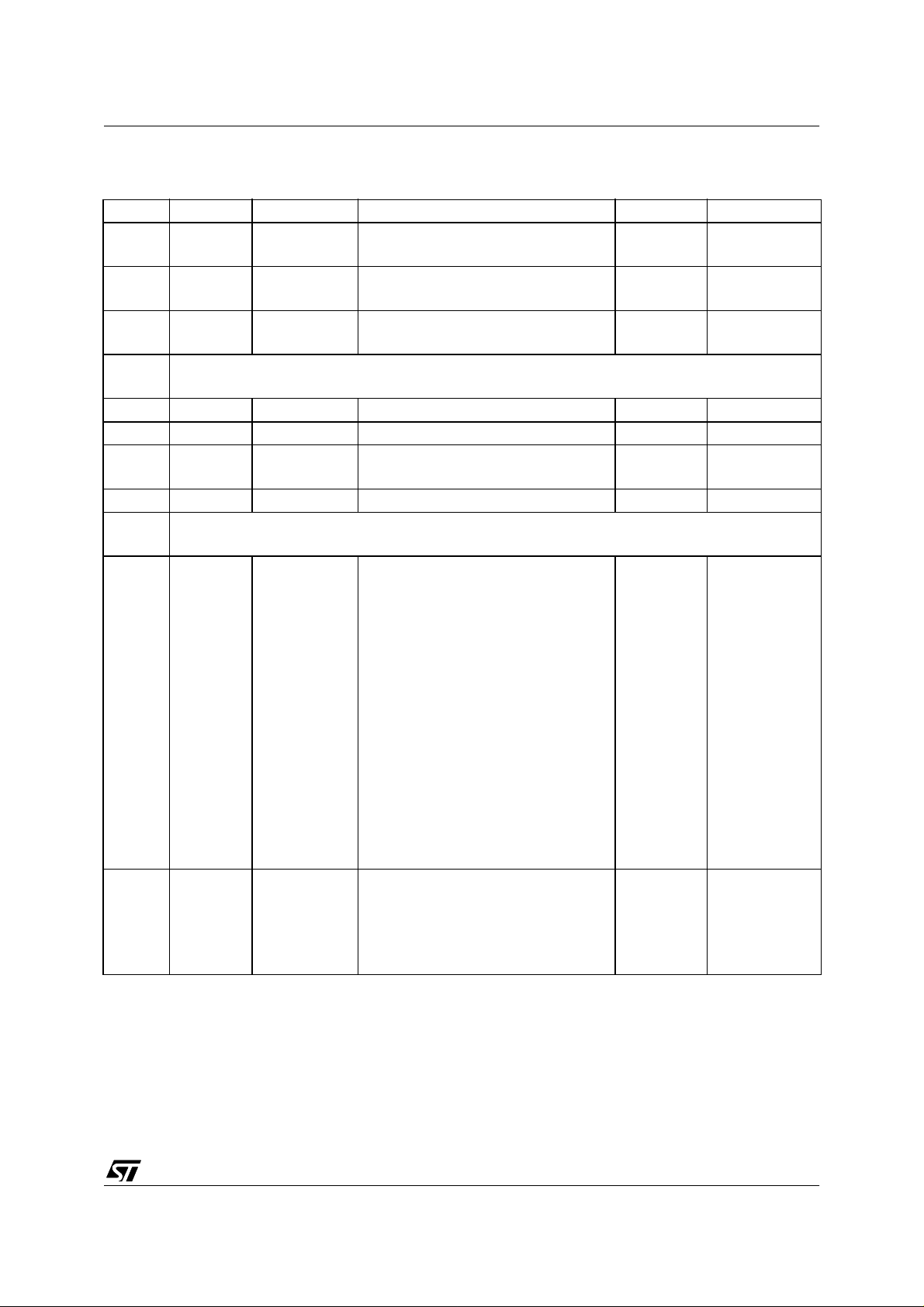
Figure 15. I nt errupt Proces s ing Fl owchart
FROM RESET
ST7263
EXECUTE INSTRUCTION
Table 7. Int errupt Mapp in g
N°
Source
Block
BIT I SET
Y
FETCH NEXT INSTRUCTION
N
RESTORE PC, X, A, CC FROM STACK
THIS CLEARS I BIT BY DEFAULT
IRET
Y
Description
N
Register
Label
N
INTERRUPT
Y
STACK PC, X, A, CC
SET I BIT
LOAD PC FROM INTERRUPT VECTOR
Priority
Order
Exit
from
HALT
Vector
Address
RESET Reset
TRAP Software Interrupt no FFFCh-FFFDh
N/A
USB End Suspend Mode ISTR
1 ITi External Interrupts ITRFRE FFF8h-FFF9h
2 TIMER Timer Peripheral Interrupts TIMSR
2
3I
CI
2
C Peripheral Interrupts
I2CSR1
I2CSR2
4 SCI SCI Peripheral Interr upts SCISR FFF2h-FFF3h
5 USB USB Peripheral Interrupts ISTR FFF0h-FFF1h
Highest
Priority
Lowest
Priority
yes FFFEh-FFFFh
yes
FFFAh-FFFBh
FFF6h-FFF7h
FFF4h-FFF5h
no
21/109

ST7263
INTERRUPTS (Cont’d)
4.1.1 Interrupt Register
INTERRUPTS REGISTER (ITRFRE)
Address: 0008h — Read/Write
Reset Value: 0000 0000 (00h)
70
IT8E IT7E IT6E IT5E IT4E IT3E IT2E IT1E
Bit 7:0 = ITiE (i=1 to 8).
Bits
.
Interrupt Enable Control
If an ITiE bit is set, the corresponding interrupt is
generated when
– a rising edge occurs on the pin PA4/IT1 or PA5/
IT2 or PB4/IT5 or PB5/IT6
or
– a falling edge occurs on the pin PA6/IT3 or PA7/
IT4 or PB6/IT7 or PB7/IT8
No interrupt is generated elsewhere.
Note: Analog input must be disabled for interrupts
coming from port B.
22/109
4.2 POWER SAVI NG MO DE S
ST7263
4.2.1 Introd uct i on
To give a large measure of flexibility to the application in terms of power consumption, two main power saving modes are implemented in the ST7.
After a RESET the normal operating mode is selected by default (RUN mode). This mode drives
the device (CPU and embedded peripherals) by
means of a master clock which is based on the
main oscillator frequency divided by 3 (f
CPU
).
From Run mode, the different power saving
modes may be selected by setting the relevant
register bits or by calling the specific ST7 software
instruction whose action depends on the oscillator
status.
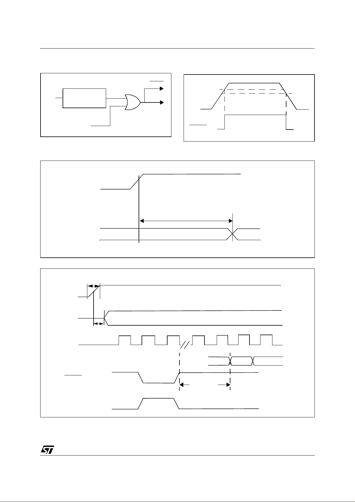
4.2.2 HALT mode
The HALT mode is the MCU lowest power consumption mode. The HALT mode is entered by executing the HALT instruction. The internal oscillator is then turned off, causing all internal processing to be stopped, including the operation of the
on-chip peripherals.
When entering HALT mode, the I bit in the Condition Code Register is cleared. Thus, any of the external interrupts (ITi or US B end suspend mode),
are allowed and if an interrupt occurs, the CPU
clock becomes active.
The MCU can exit HALT m ode on reception of either an external interrupt on ITi, an end suspend
mode interrupt coming from USB peripheral, or a
reset. The oscillat or is t hen t urned on and a stabilization time is provided before rele asing CPU operation. The stabilization time is 4096 CPU clock
cycles.
After the start up delay, the CPU continues operation by servicing the interrupt which wakes it up or
by fetching the reset vector if a reset wakes it up.
Figure 16. HAL T Mode Flow C hart
HALT INSTRUCTION
OSCILLATOR
PERIPH. CLOCK
CPU CLOCK
I-BIT
N
RESET
N
EXTERNAL
INTERRUPT*
Y
OSCILLATOR
PERIPH. CLOCK
CPU CLOCK
I-BIT
4096 CPU CLOCK
CYCLES DELAY
FETCH RESET VECTOR
OR SERVICE INTERRUPT
OFF
OFF
OFF
CLEARED
Y
ON
ON
ON
SET
Note: Before servicing an interrupt, the CC register is
pushed on the stac k. T he I -Bit i s se t du ring the interrupt routine and cleared when the CC register is
popped.
23/109
ST7263
POWER SAVING MODES (Cont’d)
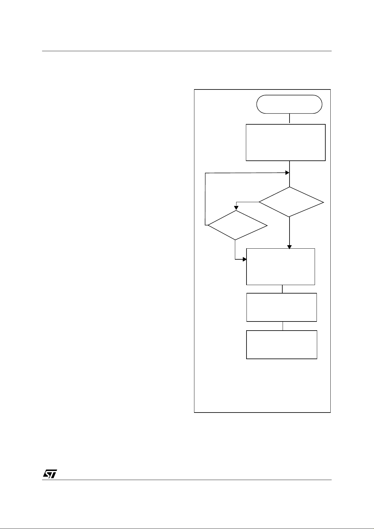
4.2.3 WAIT mode
Figure 17. WAIT Mode Flow Chart
WAIT mode places the MCU in a low power consumption mode by stopping the CPU.
This pow er s av in g mode is s elected b y ca llin g the
“WFI” ST7 software instruction.
All peripherals remain active. During WAIT mode,
the I bit of the CC register is forced to 0, to enable
all interrupts. All other registers and mem ory remain unchanged. The MCU remains in WAIT
mode until an interrupt or Reset occu rs, where upon the Program Counter branc hes to the starting
address of the interrupt or Reset service routine.
The MCU will r e main in W AIT mod e unt il a Rese t
or an Interrupt occurs, causing it to wake up.
Refer to Figure 17.
N
INTERRUPT
Y
WFI INSTRUCTION
OSCILLATOR
PERIPH. CLOCK
CPU CLOCK
I-BIT
N
RESET
OSCILLATOR
PERIPH. CLOCK
CPU CLOCK
I-BIT
ON
ON
OFF
CLEARED
Y
ON
ON
ON
SET
24/109
IF RESET
4096 CPU CLOCK
CYCLES DELAY
FETCH RESET VECTOR
OR SERVICE INTERRUPT
Note: Before servicing an interrupt, the CC register is
pushed on the sta ck. The I-Bit is s et d uring the inte rrupt routine and cleared when the CC register is
popped.
5 ON-CHIP PERIPHERALS
5.1 I/O PORTS
ST7263
5.1.1 Introd uct i on
The I/O ports offer different functional modes:
– transfer of data through digital inputs and outputs
and for specific pins:
– analog signal input (ADC)
– alternate signal input/output for the on-chip pe-
ripherals.
– external interrupt generation
An I/O port i s com pos ed of up to 8 pins. E ach pin
can be programmed independently as digital input
(with or without interrupt generation) or digital output.
5.1.2 Functi onal descri ption
Each port is associated to 2 main registers:
– Data Register (DR)
– Data Direction Register (DDR)
Each I/O pin may be programmed using the corre-
sponding register bits in DDR register: bit X corresponding to pin X of the port. The same correspondence is used for the DR register.
Table 8. I/O Pin Functi ons
DDR MODE
0 Input
1 Output
Inpu t Mode s
The input configuration is sele cted by clearing the
corresponding DDR register bit.
In this case, reading the DR register returns the
digital value applied to the external I/O pin.
Note 1: All the inputs are triggered by a Schmitt
trigg er.
Note 2: When switching from input mode to output
mode, the DR register should be written first to
output the correct value as soon as the port is configured as an output.
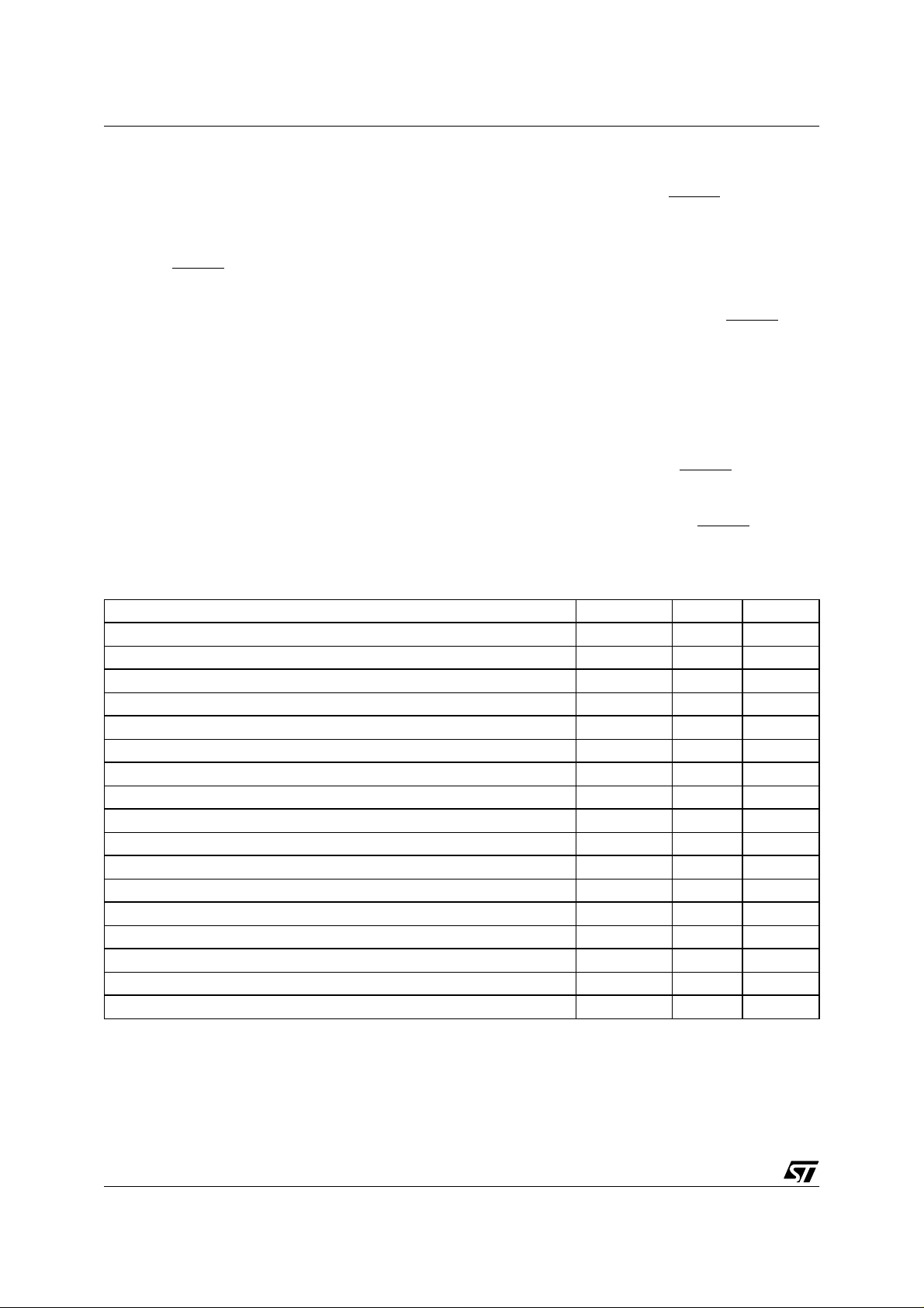
Interrupt function
When an I/O is configured in Input with Interrupt,
an event on this I/O can generate an external In-
terrupt request to the CPU. The interrupt sensitivity is given independently according to the description mentioned in the ITRFRE interrupt register.
Each pin can independently generate an Interrupt
request.
Each external interrupt vector is linked t o a dedicated group of I/O port pins (see Interrupts section). If more than one input pin is selected simultaneously as interrupt source, this is logically
ORed. For this reason if one of the interrupt pins is
tied low, it masks the other ones.
Output Mode
The pin is configured in output mode by setting the
corresponding DDR register bit (see Table 7).
In this mode, writing “0” or “1” to the DR register
applies this digital value to the I/O pin through the
latch. Then reading the DR register returns the
previously stored value.
Note: In this mode, the interrupt function is disabled.
Digital Alternate Func ti on
When an on-chip peripheral is configured to use a
pin, the alternate function is au tomatically selected. This alternate function takes priority over
standard I/O programming. When the signal is
coming from an on-chip peripheral, the I/O pin is
automatically configured in output mode (push-pull
or open drain according to the peripheral).
When the signal is goi ng to an on-chip peripheral,
the I/O pin ha s to be configured in i nput mode. In
this case, the pin’s state is a lso digitally readable
by addressing the DR register.
Notes:
1. Input pull-up configuration can cause an unex pected value at the input of the alternate peripheral input.
2. When the on-chip peripheral uses a pin as input
and output, this pin must be configured as an input
(DDR = 0).
Warning
: The alternate func tion m us t not be a cti-
vated as long as the pin is configured as input with
interrupt, in order to avoid generating spurious interrupts.
25/109

ST7263
I/O PORTS (Cont’d)
Analog Alternate Function
When the pin is used as an ADC input the I/O must
be configured as input, floating. The analog multiplexer (controlled by the ADC registers) switches
the analog voltage present o n the selected pin to
the common ana log rail which i s c onnect ed to the
ADC input.
It is recommended not to change the voltage level
or loading on any port pin while conversion is in
progress. Furthermore it i s recommended not to
have clocking pins locat ed close t o a selected analog pin.
Warning
within the limits stat ed in the A bsolute Max imum
Ratings.
5.1.3 I/O Port Implementation
The hardware implementation on each I/O port depends on the settings in the DDR register and specific feature of the I/O port such as ADC Input or
true open drain.
: The analog input voltage level must be
26/109
I/O PORTS (Cont’d)
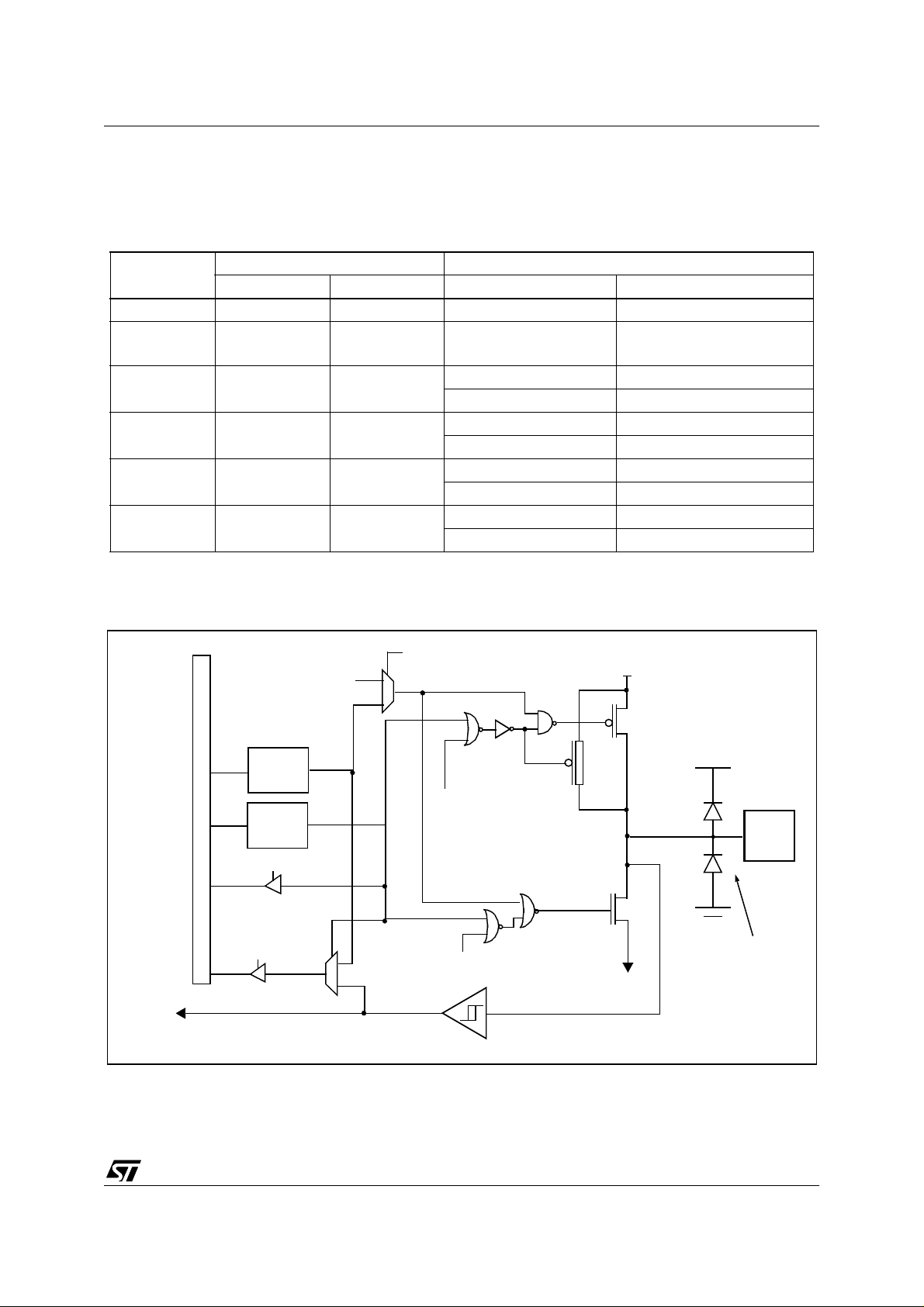
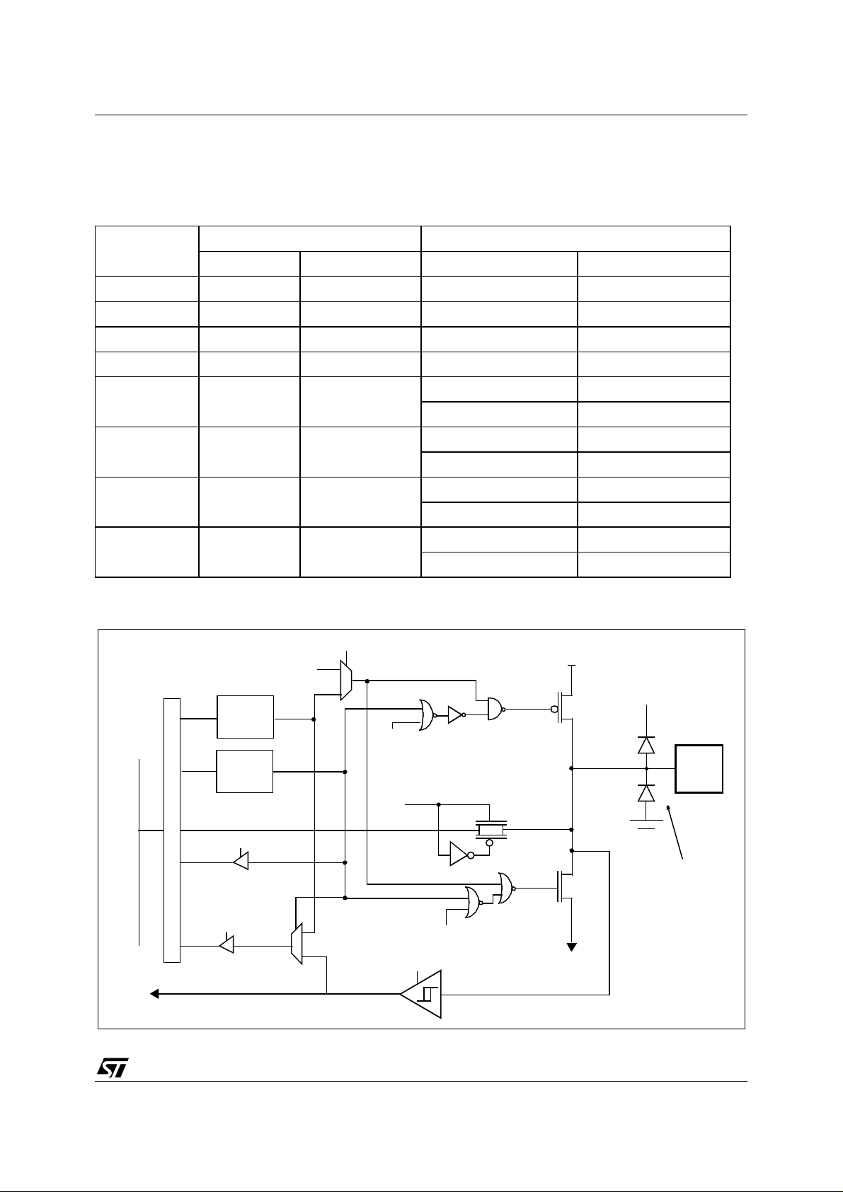
5.1.4 Port A
Table 9. Port A0, A3, A4, A5, A6, A7 Description
ST7263
PORT A
Input* Output Signal Condition
I / O Alternate Function
PA0 with pull-up push-pull MCO (Main Clock Output) MCO = 1 (MISCR)
PA3 with pull-up push-pull Timer EXTCLK
PA4 with pull-up
PA5 with pull-up
PA6 with pull-up
PA7 with pull-up
push-pull
push-pull
push-pull
push-pull
Timer ICAP1
IT1 Schmitt triggered input IT1E = 1 (ITIFRE)
Timer ICAP2
IT2 Schmitt triggered input IT2E = 1 (ITIFRE)
Timer OCMP1 OC1E = 1
IT3 Schmitt triggered input IT3E = 1 (ITIFRE)
Timer OCMP2 OC2E = 1
IT4 Schmitt triggered input IT4E = 1 (ITIFRE)
CC1 =1
CC0 = 1 (Timer CR2)
*Reset State
Figure 18. PA0, PA3, PA4, PA5, PA6, PA7 Configuration
ALTERNATE ENABLE
ALTERNATE
OUTPUT
1
0
V
DD
P-BUFFER
DATA BUS
DR SEL
ALTERNATE INPUT
DR
LATCH
DDR
LATCH
DDR SEL
V
PULL-UP
ALTERNATE ENABLE
N-BUFFER
1
0
ALTERNATE ENABLE
CMOS SCHMITT TRIGGER
V
SS
DD
PAD
DIODES
27/109
ST7263
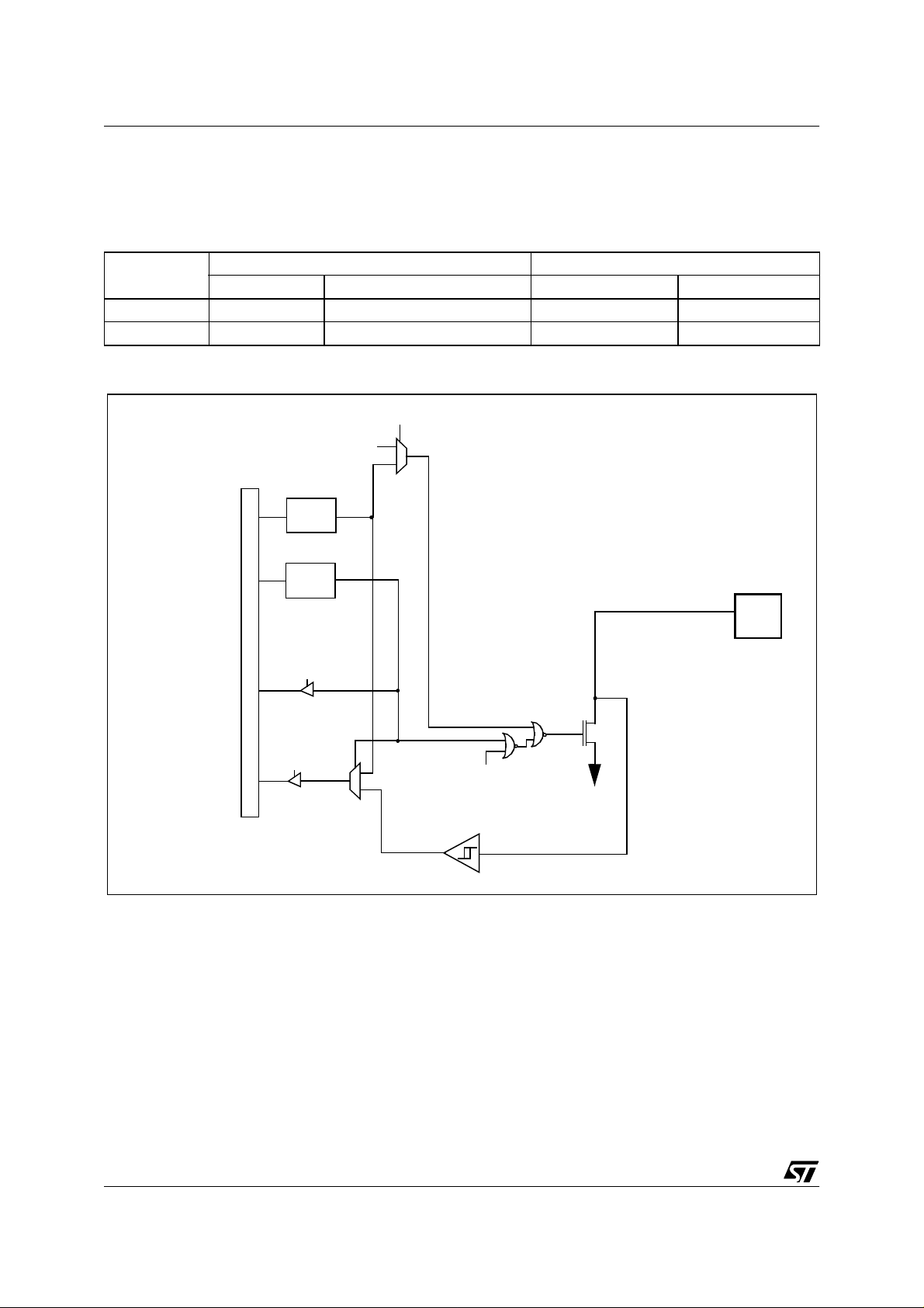
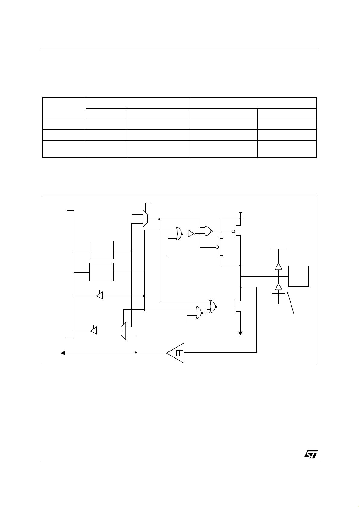
I/O PORTS (Cont’d)
Table 10. PA1, PA2 Description
PORT A
Input* Output Signal Condition
I / O Alternate Function
PA1 without pull-up Very High Current open drain SDA (I2C data) I2C enable
PA2 without pull-up Very High Current open drain SCL (I2C clock) I2C enable
*Reset State
Figure 19. PA1, PA2 Configuration
ALTERNATE ENABLE
ALTERNATE
OUTPUT
DR
LATCH
DDR
LATCH
DATA BUS
DDR SEL
1
0
PAD
DR SEL
N-BUFFER
1
0
ALTERNATE ENABLE
CMOS SCHMITT TRIGGER
V
SS
28/109
ST7263
I/O PORTS (Cont’d)
5.1.5 Port B
Table 11. Port B Description
PORT B I/O Alternate Function
Input* Output Signal Condition
PB0 without pull-up push-pull Analog input (ADC) CH[2:0] = 000 (ADCCSR)
PB1 without pull-up push-pull Analog input (ADC) CH[2:0] = 001 (ADCCSR)
PB2 without pull-up push-pull Analog input (ADC) CH[2:0]= 010 (ADCCSR)
PB3 without pull-up push-pull Analog input (ADC) CH[2:0]= 011 (ADCCSR)
PB4 without pull-up push-pull
PB5 without pull-up push-pull
PB6 without pull-up push-pull
PB7 without pull-up push-pull
*Reset State
Figure 20. Port B C onfi guration
ALTERNAT E EN ABL E
ALTERNATE
OUTPUT
DR
LATCH
DDR
COMMON ANALOG RAIL
DATA BUS
LATCH
1
0
ANALOG ENABLE
(ADC)
Analog input (ADC) CH[2:0]= 100 (ADCCS R)
IT5 Schmitt triggered input IT4E = 1 (ITIFRE)
Analog input (ADC) CH[2:0]= 101 (ADCCS R)
IT6 Schmitt triggered input IT5E = 1 (ITIFRE)
Analog input (ADC) CH[2:0]= 110 (ADCCS R)
IT7 Schmitt triggered input IT6E = 1 (ITIFRE)
Analog input (ADC) CH[2:0]= 111 (ADCCS R)
IT8 Schmitt triggered input IT7E = 1 (ITIFRE)
V
DD
P-BUFF ER
ALTERNATE EN ABLE
V
DD
PAD
ALTER N A T E INP U T
DDR SEL
DR SEL
ANALOG
SWITCH
N-BUFFER
1
0
DIGITA L EN ABL E
ALTERNATE EN ABLE
V
SS
DIODES
29/109
ST7263
I/O PORTS (Cont’d)
5.1.6 Port C
Table 12. Port C Description
PORT C
I / O Alternate Function
Input* Output Signal Condition
PC0 with pull-up push-pull RDI (SCI input)
PC1 with pull-up push-pull TDO (SCI output) SCI enable
PC2 with pull-up push-pull
USBOE (USB output enable)
USBOE =1
(MISCR)
*Reset State
Figure 21. P ort C Conf i gu ra ti on
ALTER N AT E ENABLE
ALTERNATE
OUTPUT
DR
LATCH
DATA BUS
DDR
LATCH
1
0
PULL-UP
ALTERNAT E EN ABL E
V
DD
P-BUFFER
V
DD
PAD
ALTERNATE INPUT
30/109
DDR SEL
DR SEL
N-BUFFER
1
0
ALTERNATE ENABLE
CMOS SCHMITT TRIGGER
V
SS
DIODES
 Loading...