

SGS Thomson Microelectronics ST72E311J4D0, ST72E331N4D0S, ST72E331N4D0, ST72E331J4D0S, ST72E331J4D0 Datasheet
September 1999 1/106
ST72E331
ST72T331
8-BIT MCU WITH 8 TO 16K OTP/EPROM, 256 EEPROM,
384 TO 512 BYTES RAM, ADC, WDG, SCI, SPI AND 2 TIMERS
DATASHEET
■ User Program Memory (OTP/EPROM):
8 to16K bytes
■ User EEPROM: 256 bytes
■ Data RAM: 384 to512 bytesincluding 256 bytes
of stack
■ Master Resetand Power-On Reset
■ Low Voltage Detector (LVD) Reset option
■ Run andPower Saving modes
■ 44 or32 multifunctional bidirectional I/O lines:
– 15 or 9 programmable interrupt inputs
– 8 or 4 high sink outputs
– 8 or 6 analog alternate inputs
– 13 alternate functions
– EMI filtering
■ Software or Hardware Watchdog (WDG)
■ Two 16-bit Timers, each featuring:
– 2 Input Captures
1)
– 2 Output Compares
1)
– External Clock input (on Timer A)
– PWM and Pulse Generator modes
■ Synchronous Serial Peripheral Interface (SPI)
■ Asynchronous Serial Communications Interface
(SCI)
■ 8-bit ADC with 8 channels
2)
■ 8-bit Data Manipulation
■ 63 basic Instructions and 17 main Addressing
Modes
■ 8 x8 Unsigned Multiply Instruction
■ True BitManipulation
■ Complete Development Support on DOS/
WINDOWSTMReal-Time Emulator
■ Full Software Package on DOS/WINDOWS
TM
(C-Compiler, Cross-Assembler, Debugger)
Notes:
1. One only on Timer A.
2. Six channels only for ST72T331J.
Device Summary
Note: The ROM versions are supportedby the ST72334 family.
TQFP44
PSDIP42
PSDIP56
CSDIP42W
CSDIP56W
TQFP64
(See ordering information at the end of datashee
Features ST72T331J2 ST72T331J4 ST72T331N2 ST72T331N4
Program Memory - bytes 8K 16K 8K 16K
EEPROM - bytes 256
RAM (stack) - bytes 384 (256) 512 (256) 384 (256) 512 (256)
Peripherals Watchdog, Timers, SPI, SCI, ADC and optional Low Voltage Detector Reset
Operating Supply 3 to 5.5 V
CPU Frequency 8MHz max (16MHz oscillator) - 4MHz max over 85°C
Temperature Range - 40°C to + 125°C
Package TQFP44 -SDIP42 TQFP64 -SDIP56
1
Rev. 1.7

2/106
Table of Contents
95
ST72E331/ST72T331 . . . . . . . . . . . .......................1
1 GENERAL DESCRIPTION . . . . . . ................................................ 5
1.1 INTRODUCTION . . . . . . . . . . . . . ............................................ 5
1.2 PIN DESCRIPTION . . ..................................................... 6
1.3 EXTERNAL CONNECTIONS . . . . . . . . . .. . . . . . . . . . . .. . . . . . . . . . . . . . . . . ........ 10
1.4 MEMORY MAP . . . .. . . . . . ............................................... 11
1.5 OPTION BYTE . . . . .. ....................................................14
2 CENTRAL PROCESSING UNIT . . ............................................... 15
2.1 INTRODUCTION . . . . . . . . . . . . . ...........................................15
2.2 MAIN FEATURES . . . .. . . . . . .. . . . . . . . . . . . . ............................... 15
2.3 CPU REGISTERS . . . .................................................... 15
3 CLOCKS, RESET, INTERRUPTS & POWER SAVING MODES . . . . . .. . . . . . . ........... 18
3.1 CLOCK SYSTEM . . . . . .. . . . . . . ...........................................18
3.1.1 General Description . . . .. ............................................18
3.1.2 External Clock . . . . . . . . . . . . . ........................................ 18
3.2 RESET . . . . . . . . . . .. .. . . . . . . . . . . .. .. . . . . . ............................... 19
3.2.1 Introduction . . . .................................................... 19
3.2.2 External Reset . . . . . . ...............................................19
3.2.3 Reset Operation . . . . . . . . . . . . . . .. . . . . . . . .. ........................... 19
3.2.4 Low Voltage DetectorReset . . . . . . . . . . . . . . .. . . . . . . .. . . . . . . .. . . . . . . . . . . 20
3.3 INTERRUPTS . . . .. . . . . . . . . . . . . . . . . . . . . . . . . . . . .. . . . . . . . . .. . . . . . . . . .. . . . . 21
3.4 POWER SAVING MODES . . . . . . . . . . . . . . . . . . . . . . . .. . . . . . . . . . . .. . . . . ........ 24
3.4.1 Introduction . . . .................................................... 24
3.4.2 Slow Mode . . .. . . . . . . . . . . . . . . . . . . . ................................. 24
3.4.3 Wait Mode . . . . . . . . .. . . . . . . ........................................ 24
3.4.4 Halt Mode . . . . . .................................................... 25
3.5 MISCELLANEOUS REGISTER . . . . .. .. . . . ..................................26
4 ON-CHIP PERIPHERALS . . . . . . . . . . . ...........................................27
4.1 I/O PORTS . . . . . . . . . . . . . . . . . . ........................................... 27
4.1.1 Introduction . . . .................................................... 27
4.1.2 Functional Description . . . . ...........................................27
4.1.3 I/O Port Implementation . . . . . . . . . . . . . . .. . . . ........................... 28
4.1.4 Register Description . . . . . . ...........................................31
4.2 EEPROM(EEP)......................................................... 33
4.2.1 Introduction . . . .................................................... 33
4.2.2 Main Features . .. .. . ...............................................33
4.2.3 Functional description . . .. . . . . . .. . . . . . . . . . ........................... 34
4.2.4 Low Power Modes . . . ............................................... 36
4.2.5 Interrupts . . . . . .. . . . . . . . . . . . . . . . . . ................................. 36
4.2.6 Register Description . . . . . . ...........................................36
4.3 WATCHDOG TIMER (WDG) . . . . . . . . . . . . . . . . . . . . . . . . . . . . . . . . . . .. . . . . . . . . . . . 37
4.3.1 Introduction . . . .................................................... 37
4.3.2 Main Features . .. .. . ...............................................37
4.3.3 Functional Description . . . . ...........................................37
4.3.4 Hardware Watchdog Option . .. . . . . . . . ................................. 38
2

3/106
Table of Contents
4.3.5 Low Power Modes . . . ............................................... 38
4.3.6 Interrupts . . . . . .. . . . . . . . . . . . . . . . . . ................................. 38
4.3.7 Register Description . . . . . . ...........................................38
4.4 16-BIT TIMER . . . . . . . .. . . . . . . . .. ........................................40
4.4.1 Introduction . . . .................................................... 40
4.4.2 Main Features . .. .. . ...............................................40
4.4.3 Functional Description . . . . ...........................................40
4.4.4 Low Power Modes . . ............................................... 51
4.4.5 Interrupts . . .. . ....................................................51
4.4.6 Register Description . . . . . . ...........................................52
4.5 SERIAL COMMUNICATIONS INTERFACE (SCI) . . . . . . . . . . . . . . . . . . . . . . . . . .. . . . . 57
4.5.1 Introduction . . . .................................................... 57
4.5.2 Main Features . .. .. . ...............................................57
4.5.3 General Description . . . .. ............................................57
4.5.4 Functional Description . . . . ...........................................59
4.5.5 Low Power Modes . . . ............................................... 64
4.5.6 Interrupts . . . . . .. . . . . . . . . . . . . . . . . . ................................. 64
4.5.7 Register Description . . . . . . ...........................................65
4.6 SERIAL PERIPHERAL INTERFACE (SPI) . . . . . . . . . . .. . . . . . . . . . . . . ............69
4.6.1 Introduction . . . .................................................... 69
4.6.2 Main Features . .. .. . ...............................................69
4.6.3 General description . . . . . . . . . . . . . . . . .. . . .. . . . . . . . . . . . . . . . . . . . . . . . . . . . 69
4.6.4 Functional Description . . . . ...........................................71
4.6.5 Low Power Modes . . . ............................................... 78
4.6.6 Interrupts . . .. . ....................................................78
4.6.7 Register Description . . . . . . ...........................................79
4.7 8-BIT A/D CONVERTER (ADC) . . . . . .. .. . . . . . . . . . ........................... 82
4.7.1 Introduction . . . .................................................... 82
4.7.2 Main Features . .. .. . ...............................................82
4.7.3 Functional Description . . . . ...........................................83
4.7.4 Low Power Modes . . . ............................................... 83
4.7.5 Interrupts . . . . . .. . . . . . . . . . . . . . . . . . ................................. 83
4.7.6 Register Description . . . . . . ...........................................84
5 INSTRUCTION SET .. . . . . . . . . . . . . . . . . ........................................ 85
5.1 ST7 ADDRESSING MODES . . . . . . . . . .. . . . . . . . . . . . . . . . . . . . . . . . .. . . . . . . . . . . . 85
5.1.1 Inherent . . . . . . . . . . . ...............................................86
5.1.2 Immediate . .. . . . .. . . . . . . . .. . . . . . . . . . . . . . .. . . . . . . .. . . . . . . . . . . . . . . . . 86
5.1.3 Direct . ........................................................... 86
5.1.4 Indexed (No Offset, Short, Long) . . . . . . . . . . . . ........................... 86
5.1.5 Indirect (Short, Long) . . . . .. . . . . . . . . . .. . . . . . . . . . . . . . . . . . . . . . . .. . . . . . . . 86
5.1.6 Indirect Indexed (Short,Long) . ........................................87
5.1.7 Relative mode (Direct,Indirect) . . . .. . . . . . . . .. . . . . . . . . . . .. . . . . . . . . . .. . . . 87
5.2 INSTRUCTION GROUPS . . .. . . . . . . . . . . .. ................................. 88
6 ELECTRICALCHARACTERISTICS . . . . . . . . .. . . . . . . .............................. 91
6.1 ABSOLUTE MAXIMUM RATINGS . . . ........................................91
6.2 RECOMMENDED OPERATING CONDITIONS . . . .............................. 92
6.3 RESET CHARACTERISTICS . . . . . . . . . . .................................... 93
3

4/106
ST72E331 ST72T331
6.4 OSCILLATOR CHARACTERISTICS . . . . . . . . . . ............................... 93
6.5 DC ELECTRICAL CHARACTERISTICS . . . . . .. . . . .. . . . . . . . .. . . . . . . ...........94
6.6 PERIPHERAL CHARACTERISTICS . . . . . . . ..................................95
7 GENERAL INFORMATION . . . . . . . . . . ..........................................101
7.1 EPROM ERASURE . . .. . . . . . . . . . . .. .. . . . . . . ............................. 101
7.2 PACKAGE MECHANICALDATA . . .. . . . . . . . . . . . . . .......................... 102
7.3 ORDERING INFORMATION . . . . . .. . . . .. . ................................. 105
8 SUMMARY OF CHANGES . . . . . . . . . . . . . . . . . . . . . . . . . . . . . . . . . . . . . . . . . . . . . . . . . . . . 106
4
5/106
ST72E331 ST72T331
1 GENERAL DESCRIPTION
1.1 INTRODUCTION
The ST72T331 HCMOS Microcontroller Unit
(MCU) is a member of the ST7 family.The device
is based on an industry-standard 8-bit core and
features an enhanced instruction set. The device
is normally operated at a 16 MHz oscillator frequency. Under software control, the ST72T331
may be placed in either Wait, Slow or Halt modes,
thus reducing power consumption. The enhanced
instruction set and addressing modes afford real
programming potential. In addition to standard
8-bit data management, the ST72T331 features
true bit manipulation, 8x8 unsigned multiplication
and indirect addressing modeson the whole memory. The device includes a low consumption and
fast start on-chip oscillator, CPU, program memory (OTP/EPROM versions), EEPROM, RAM, 44
(QFP64 and SDIP56) or 32 (QFP44 and SDIP42)
I/O lines, a Low Voltage Detector (LVD) and the
following on-chip peripherals: Analog-to-Digital
converter (ADC) with 8 (QFP64, SDIP56) or 6
(QFP44, SDIP42) multiplexed analog inputs, industry standard synchronous SPI and asynchronous SCI serial interfaces, digital Watchdog, two
independent 16-bit Timers, one featuring an External Clock Input, and both featuring Pulse Generator capabilities, 2 Input Captures and 2 Output
Compares (only 1 Input Capture and 1 Output
Compare on Timer A).
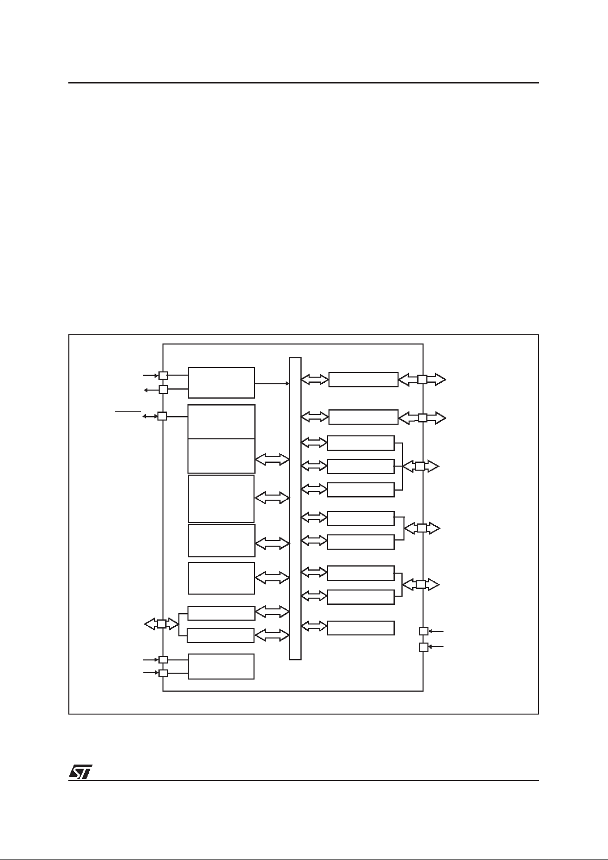
Figure 1. ST72T331 Block Diagram
8-BIT CORE
ALU
ADDRESS AND DATA BUS
OSCIN
OSCOUT
RESET
PORT B
TIMER B
PORT C
SPI
PORT E
SCI
PORT D
8-BIT ADC
WATCHDOG
PB0 -> PB7
PC0 -> PC7
PE0 -> PE7
PD0 -> PD7
OSC
Internal
CLOCK
CONTROL
RAM
(384 - 512 Bytes)
PORT F
PF0 -> PF2,4,6,7
TIMER A
PORT A
PA0 -> PA7
V
SSA
V
DDA
(6 bits forST72T331N)
(6 bits)
EEPROM
(256 Bytes)
AND LVD
(2 bits for ST72T331J)
(8 bits for ST72T331N)
(6 bits for ST72T331J)
(8 bits for ST72T331N)
(5 bits for ST72T331J)
(8 bits)
(8 bits for ST72T331N)
(5 bits for ST72T331J)
V
SS
V
DD
POWER
SUPPLY
PROGRAM
(8 - 16K Bytes)
MEMORY
5
6/106
ST72E331 ST72T331
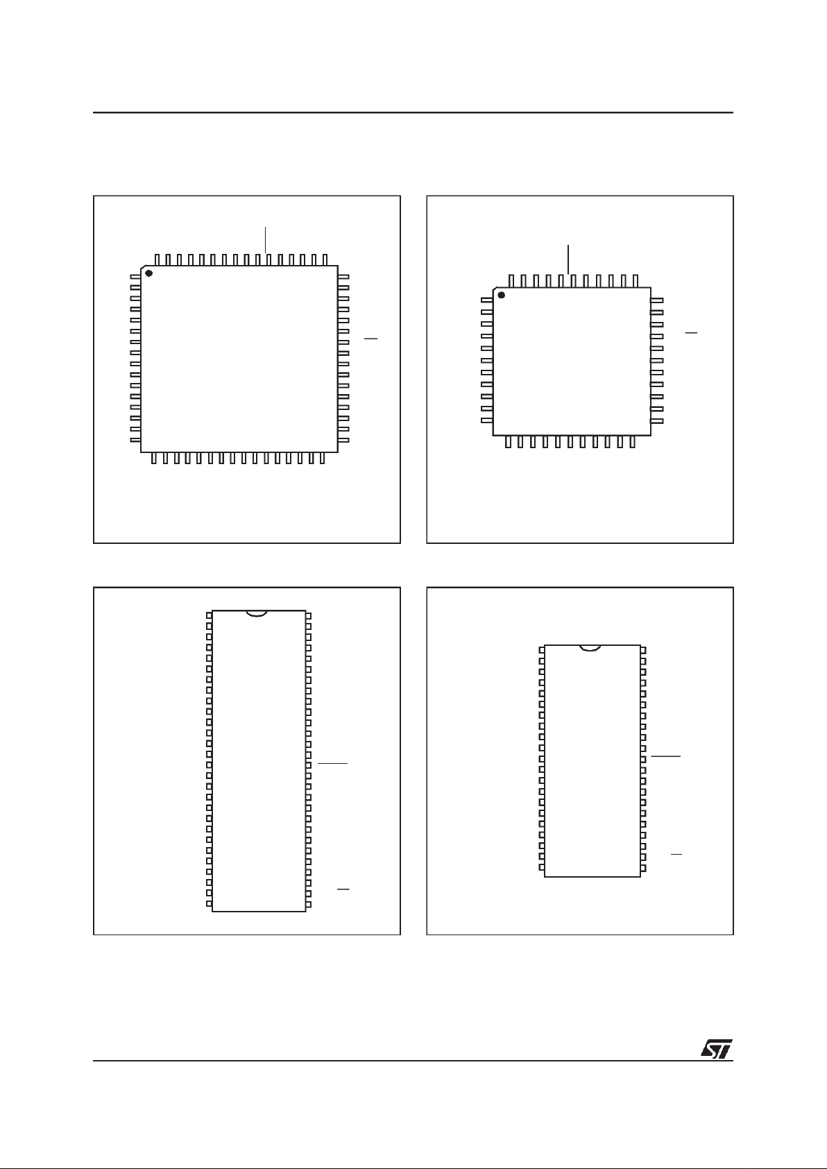
1.2 PIN DESCRIPTION
Figure 2. 64-Pin Thin QFP Package Pinout
Figure 3. 56-Pin Shrink DIPPackage Pinout
Figure 4. 44-Pin Thin QFP Package Pinout
Figure 5. 42-Pin Shrink DIP Package Pinout
1
2
3
4
5
6
7
8
9
10
11
12
13
14
15
16
48
47
46
45
44
43
42
41
40
39
38
37
36
35
34
33
64 6362 6160 5958 5756 55 54 53 5251 50 49
17 18192021 2223 24 29 30313225 262728
PE4
PE5
PE6
PE7
PB0
PB1
PB2
PB3
PB4
PB5
PB6
PB7
AIN0/PD0
AIN1/PD1
AIN2/PD2
AIN3/PD3
V
SS_1
V
DD_1
PA3
PA2
PA1
PA0
PC7/SS
PC6/SCK
PC5/MOSI
PC4/MISO
PC3/ICAP1_B
PC2/ICAP2_B
PC1/OCMP1_B
PC0/OCMP2_B
V
SS_0
V
DD_0
AIN4/PD4
AIN5/PD5
AIN6/PD6
AIN7/PD7
V
DDA
V
SSA
V
DD_3
V
SS_3
CLKOUT/PF0
PF1
PF2
NC
OCMP1_A/PF4
NC
ICAP1_A/PF6
EXTCLK_A/PF7
NCNCPE1/RDI
PE0/TDO
V
DD_2
OSCIN
OSCOUT
V
SS_2
NCNCRESET
TEST/V
PP
1)
PA7
PA6
PA5
PA4
(EI0)
(EI0)
(EI0)
(EI0)
(EI2)
(EI2)
(EI2)
(EI2)
(EI3)
(EI3)
(EI3)
(EI3)
(EI1)
(EI1)
(EI1)
1. VPPon EPR OM/OTP only
15 (EI1)
16 (EI1)
17 (EI1)
18
19
20
21
22
23
24
25
26
27
28 29
30
(EI0) 31
(EI0) 32
(EI0) 33
(EI0) 34
CLKOUT/PF0
PF1
PF2
OCMP1_A/PF4
ICAP1_A/PF6
PC1/OCMP1_B
PC2/ICAP2_B
EXTCLK_A/PF7
V
DD_0
V
SS_0
RESET
TEST/V
PP
1)
PA7
PA6
PA5
PA2
PA1
PA0
PC7/SS
PC6/SCK
42
41
40
39
38
37
36
35
PC0/OCMP2_B
PC3/ICAP1_B
PC4/MISO
PC5/MOSI
PA4
V
SS_1
V
DD_1
PA3
1 (EI3)
2 (EI3)
3 (EI3)
4 (EI3)
5
6
7
8
9
10
11
12
13
14
43
44
45
46
47
48
PB4
PB5
PB6
PB7
AIN0/PD0
AIN5/PD5
AIN6/PD6
AIN1/PD1
AIN2/PD2
AIN3/PD3
PB3
PB2
PB1
PB0
PE7
PE0/TD0
V
DD_2
OSCIN
OSCOUT
V
SS_2
(EI2) 56
(EI2) 55
(EI2) 54
(EI2) 53
52
51
50
49
AIN4/PD4
AIN7/PD7
V
DDA
V
SSA
PE6
PE5
PE4
PE1/RDI
1.VPPon EPROM/OTP only
1
2
3
4
5
6
7
8
9
10
11
33
32
31
30
29
28
27
26
25
24
23
44 43 42 41 40 39 38 37 36 35 34
12 13 14 15 16 17 18 19
(EI1)
(EI1)
(EI1)
20 21 22
CLKOUT/PF0
PF1
PF2
OCMP1_A/PF4
ICAP1_A/PF6
PC1/OCMP1_B
PC2/ICAP2_B
EXTCLK_A/PF7
V
DD_0
V
SS_0
PC0/OCMP2_B
PC3/ICAP1_B
PC4/MISO
PC5/MOSI
PB4
AIN0/PD0
AIN5/PD5
AIN1/PD1
AIN2/PD2
AIN3/PD3
AIN4/PD4
V
DDA
V
SSA
RESET
TEST/V
PP
1)
PA7
PA6
PA5
PC7/SS
PC6/SCK
PA4
V
SS_1
V
DD_1
PA3
PB3
PB2
PB1
PB0
PE0/TD0
V
DD_2
OSCIN
OSCOUT
V
SS_2
PE1/RDI
(EI3)
(EI2)
(EI2)
(EI2)
(EI2)
(EI0)
1. VPPon EPROM/OTP only
15
16
17
18
19
20
21
CLKOUT/PF0
PF1
PF2
OCMP1_A/PF4
ICAP1_A/PF6
PC1/OCMP1_B
PC2/ICAP2_B
EXTCLK_A/PF7
RESET
TEST/V
PP
1)
PA7
PA6
PA5
PC7/SS
PC6/SCK
28
27
26
25
24
23
22
PC0/OCMP2_B
PC3/ICAP1_B
PC4/MISO
PC5/MOSI
PA4
V
SS_1
V
DD_1
PA3
1
2
3
4
5
6
7
8
9
10
11
12
13
14
29
30
31
32
33
34
PB4
AIN0/PD0
AIN5/PD5
AIN1/PD1
AIN2/PD2
AIN3/PD3
PB3
PB2
PB1
PB0
PE0/TD0
V
DD_2
OSCIN
OSCOUT
V
SS_2
42
41
40
39
38
37
36
35
AIN4/PD4
V
DDA
V
SSA
PE1/RDI
(EI3)
(EI1)
(EI1)
(EI1)
(EI0)
(EI2)
(EI2)
(EI2)
(EI2)
1. VPPon EPROM/OTP only
6

7/106
ST72E331 ST72T331
Table 1. ST72T331Nx Pin Description
Pin n°
QFP64
Pin n°
SDIP56
Pin Name Type Description Remarks
1 49 PE4 I/O Port E4 High Sink
2 50 PE5 I/O Port E5 High Sink
3 51 PE6 I/O Port E6 High Sink
4 52 PE7 I/O Port E7 High Sink
5 53 PB0 I/O Port B0 External Interrupt: EI2
6 54 PB1 I/O Port B1 External Interrupt: EI2
7 55 PB2 I/O Port B2 External Interrupt: EI2
8 56 PB3 I/O Port B3 External Interrupt: EI2
9 1 PB4 I/O Port B4 External Interrupt: EI3
10 2 PB5 I/O Port B5 External Interrupt: EI3
11 3 PB6 I/O Port B6 External Interrupt: EI3
12 4 PB7 I/O Port B7 External Interrupt: EI3
13 5 PD0/AIN0 I/O Port D0 or ADC Analog Input 0
14 6 PD1/AIN1 I/O Port D1 or ADC Analog Input 1
15 7 PD2/AIN2 I/O Port D2 or ADC Analog Input 2
16 8 PD3/AIN3 I/O Port D3 or ADC Analog Input 3
17 9 PD4/AIN4 I/O Port D4 or ADC Analog Input 4
18 10 PD5/AIN5 I/O Port D5 or ADC Analog Input 5
19 11 PD6/AIN6 I/O Port D6 or ADC Analog Input 6
20 12 PD7/AIN7 I/O Port D7 or ADC Analog Input 7
21 13 V
DDA
S Power Supply for analog peripheral (ADC)
22 14 V
SSA
S Ground for analog peripheral (ADC)
23 V
DD_3
S Main power supply
24 V
SS_3
S Ground
25 15 PF0/CLKOUT I/O Port F0 or CPU Clock Output External Interrupt: EI1
26 16 PF1 I/O Port F1 External Interrupt: EI1
27 17 PF2 I/O Port F2 External Interrupt: EI1
28 NC Not Connected
29 18 PF4/OCMP1_A I/O Port F4 or Timer A Output Compare 1
30 NC Not Connected
31 19 PF6/ICAP1_A I/O Port F6 or Timer AInput Capture 1
32 20 PF7/EXTCLK_A I/O Port F7 or External Clock on Timer A
33 21 V
DD_0
S Main power supply
34 22 V
SS_0
S Ground
35 23 PC0/OCMP2_B I/O Port C0 or Timer B Output Compare 2
36 24 PC1/OCMP1_B I/O Port C1 or Timer B Output Compare 1
37 25 PC2/ICAP2_B I/O Port C2 or Timer B Input Capture 2
38 26 PC3/ICAP1_B I/O Port C3 or Timer B Input Capture 1
39 27 PC4/MISO I/O Port C4 or SPI Master In/ Slave Out Data
40 28 PC5/MOSI I/O Port C5 or SPI Master Out/ Slave In Data
41 29 PC6/SCK I/O Port C6 or SPI Serial Clock
42 30 PC7/SS I/O Port C7 or SPI Slave Select
43 31 PA0 I/O Port A0 External Interrupt: EI0
7
8/106
ST72E331 ST72T331
Note 1:VPPon EPROM/OTP only.
Table 2. ST72T331Jx Pin Description
44 32 PA1 I/O Port A1 External Interrupt: EI0
45 33 PA2 I/O Port A2 External Interrupt: EI0
46 34 PA3 I/O Port A3 External Interrupt: EI0
47 35 V
DD_1
S Main power supply
48 36 V
SS_1
S Ground
49 37 PA4 I/O Port A4 High Sink
50 38 PA5 I/O Port A5 High Sink
51 39 PA6 I/O Port A6 High Sink
52 40 PA7 I/O Port A7 High Sink
53 41 TEST/V
PP
1)
S
Test mode pin . In the EPROM programming
mode, thispin acts as the programming voltage
input V
PP.
This pin must be tied
low in user mode
54 42 RESET I/O Bidirectional. Active low. Top priority non maskable interrupt.
55 NC Not Connected
56 NC Not Connected
57 43 V
SS_2
S Ground
58 44 OSCOUT O
Input/Output Oscillator pin. These pins connect a parallel-resonant
crystal, or an external source to theon-chip oscillator.
59 45 OSCIN I
60 46 V
DD_2
S Main power supply
61 47 PE0/TDO I/O Port E1 or SCI Transmit Data Out
62 48 PE1/RDI I/O Port E1 or SCI Receive Data In
63 NC Not Connected
64 NC Not Connected
Pin n°
QFP64
Pin n°
SDIP56
Pin Name
Type
Description Remarks
Pin n°
QFP44
Pin n°
SDIP42
Pin Name Type Description Remarks
1 38 PE1/RDI I/O Port E1 or SCI Receive Data In
2 39 PB0 I/O Port B0 External Interrupt: EI2
3 40 PB1 I/O Port B1 External Interrupt: EI2
4 41 PB2 I/O Port B2 External Interrupt: EI2
5 42 PB3 I/O Port B3 External Interrupt: EI2
6 1 PB4 I/O Port B4 External Interrupt: EI3
7 2 PD0/AIN0 I/O Port D0 or ADC Analog Input 0
8 3 PD1/AIN1 I/O Port D1 or ADC Analog Input 1
9 4 PD2/AIN2 I/O Port D2 or ADC Analog Input 2
10 5 PD3/AIN3 I/O Port D3 or ADC Analog Input 3
11 6 PD4/AIN4 I/O Port D4 or ADC Analog Input 4
12 7 PD5/AIN5 I/O Port D5 or ADC Analog Input 5
13 8 V
DDA
S Power Supply for analog peripheral (ADC)
14 9 V
SSA
S Ground for analog peripheral (ADC)
15 10 PF0/CLKOUT I/O Port F0 or CPU Clock Output External Interrupt: EI1
16 11 PF1 I/O Port F1 External Interrupt: EI1
17 12 PF2 I/O Port F2 External Interrupt: EI1
8

9/106
ST72E331 ST72T331
Note 1:VPPon EPROM/OTP only.
18 13 PF4/OCMP1_A I/O Port F4 or Timer A Output Compare 1
19 14 PF6/ICAP1_A I/O Port F6 or Timer A Input Capture 1
20 15 PF7/EXTCLK_A I/O Port F7 or External Clock on Timer A
21 V
DD_0
S Main power supply
22 V
SS_0
S Ground
23 16 PC0/OCMP2_B I/O Port C0 or Timer B Output Compare 2
24 17 PC1/OCMP1_B I/O Port C1 or Timer B Output Compare 1
25 18 PC2/ICAP2_B I/O Port C2 or Timer B Input Capture 2
26 19 PC3/ICAP1_B I/O Port C3 or Timer B Input Capture 1
27 20 PC4/MISO I/O Port C4 or SPI Master In / Slave Out Data
28 21 PC5/MOSI I/O Port C5 or SPI Master Out / Slave In Data
29 22 PC6/SCK I/O Port C6or SPI Serial Clock
30 23 PC7/SS I/O Port C7 or SPI Slave Select
31 24 PA3 I/O Port A3 External Interrupt: EI0
32 25 V
DD_1
S Main power supply
33 26 V
SS_1
S Ground
34 27 PA4 I/O Port A4 High Sink
35 28 PA5 I/O Port A5 High Sink
36 29 PA6 I/O Port A6 High Sink
37 30 PA7 I/O Port A7 High Sink
38 31 TEST/V
PP
1)
S
Test mode pin. In the EPROM programming
mode, this pin acts as the programming
voltage input V
PP.
This pin must be tied
low in user mode
39 32 RESET I/O Bidirectional. Active low. Top priority nonmaskable interrupt.
40 33 V
SS_2
S Ground
41 34 OSCOUT O
Input/Output Oscillator pin. These pins connect a parallel-resonant
crystal, or an external source to the on-chip oscillator.
42 35 OSCIN I
43 36 V
DD_2
S Main power supply
44 37 PE0/TDO I/O Port E0or SCI Transmit Data Out
Pin n°
QFP44
Pin n°
SDIP42
Pin Name Type Description Remarks
9
10/106
ST72E331 ST72T331
1.3 EXTERNAL CONNECTIONS
The following figure shows the recommended external connections for the device.
The VPPpin is only used for programming OTP
and EPROM devices and must betied to ground in
user mode.
The 10 nF and 0.1 µF decoupling capacitors on
the power supply lines are a suggested EMC performance/cost tradeoff.
The external reset network is intended to protect
the device against parasitic resets, especially in
noisy environments.
Unused I/Os should be tied high to avoid any unnecessary power consumption on floating lines.
An alternative solution is to program the unused
ports as inputs with pull-up.
Figure 6. Recommended External Connections
V
PP
V
DD
V
SS
OSCIN
OSCOUT
RESET
V
DD
0.1µF
+
See
Clocks
Section
V
DD
0.1µF
0.1µF
EXTERNAL RESET CIRCUIT
Or configure unused I/O ports
Unused I/O
10nF
4.7K
10K
by software as input with pull-up
V
DD
V
DDA
V
SSA
See
A/D Converter
Section
Detector (LVD) is used
Optional if Low Voltage
10
11/106
ST72E331 ST72T331
1.4 MEMORY MAP
Figure 7. Program Memory Map
Table 3. Interrupt Vector Map
Vector Address Description Remarks
FFE0-FFE1h
FFE2-FFE3h
FFE4-FFE5h
FFE6-FFE7h
FFE8-FFE9h
FFEA-FFEBh
FFEC-FFEDh
FFEE-FFEFh
FFF0-FFF1h
FFF2-FFF3h
FFF4-FFF5h
FFF6-FFF7h
FFF8-FFF9h
FFFA-FFFBh
FFFC-FFFDh
FFFE-FFFFh
Not Used
Not Used
EEPROM Interrupt Vector
SCI Interrupt Vector
TIMER B Interrupt Vector
TIMER A Interrupt Vector
SPI interrupt vector
Not Used
External Interrupt Vector EI3
External Interrupt Vector EI2
External Interrupt Vector EI1
External Interrupt Vector EI0
Not Used
Not Used
TRAP (software) Interrupt Vector
RESET Vector
Internal Interrupt
Internal Interrupt
Internal Interrupt
Internal Interrupt
Internal Interrupt
External Interrupt
External Interrupt
External Interrupt
External Interrupt
CPU Interrupt
0000h
Interrupt & Reset Vectors
HW Registers
027Fh
0080h
Short Addressing
RAM (zero page)
16-bit Addressing
RAM
007Fh
0200h / 0280h
0BFFh
Reserved
0080h
(see Table 4)
0C00h
FFDFh
FFE0h
FFFFh
(see Table 3)
027Fh
C000h
Reserved
EEPROM256 Bytes
0CFFh
0D00h
BFFFh
00FFh
0100h
01FFh
0200h
8K Bytes
E000h
16K Bytes
Program
Short Addressing
RAM (zero page)
0080h
00FFh
01FFh
01FFh
384 Bytes RAM
512 Bytes RAM
256 Bytes Stack/
16-bit Addressing RAM
256 Bytes Stack/
16-bit Addressing RAM
0100h
Memory
Program
Memory
11
12/106
ST72E331 ST72T331
Table 4. Hardware Register Memory Map
Address Block
Register
Label
Register Name
Reset
Status
Remarks
0000h
0001h
0002h
Port A
PADR
PADDR
PAOR
Data Register
Data Direction Register
Option Register
00h
00h
00h
R/W
R/W
R/W
1)
0003h Reserved Area (1 byte)
0004h
0005h
0006h
Port C
PCDR
PCDDR
PCOR
Data Register
Data Direction Register
Option Register
00h
00h
00h
R/W
R/W
R/W
0007h Reserved Area (1 byte)
0008h
0009h
000Ah
Port B
PBDR
PBDDR
PBOR
Data Register
Data Direction Register
Option Register
00h
00h
00h
R/W
R/W
R/W
1)
000Bh Reserved Area (1 byte)
000Ch
000Dh
000Eh
Port E
PEDR
PEDDR
PEOR
Data Register
Data Direction Register
Option Register
00h
00h
0Ch
R/W
R/W
R/W
1)
000Fh Reserved Area (1 byte)
0010h
0011h
0012h
Port D
PDDR
PDDDR
PDOR
Data Register
Data Direction Register
Option Register
00h
00h
00h
R/W
R/W
R/W
1)
0013h Reserved Area (1 byte)
0014h
0015h
0016h
Port F
PFDR
PFDDR
PFOR
Data Register
Data Direction Register
Option Register
00h
00h
28h
R/W
R/W
R/W
1)
0017h to
001Fh
Reserved Area (9 bytes)
0020h MISCR Miscellaneous Register 00h
0021h
0022h
0023h
SPI
SPIDR
SPICR
SPISR
SPI Data I/O Register
SPI Control Register
SPI Status Register
xxh
xxh
00h
R/W
R/W
Read Only
0024h to
0029h
Reserved Area (6 bytes)
002Ah
002Bh
WDG
WDGCR
WDGSR
Watchdog Control Register
Watchdog Status Register
7Fh
00h
R/W
R/W
3)
002Ch EEPROM EEPCR EEPROM Control Register 00h R/W Register
002Dh to
0030h
Reserved Area (4 bytes)
12

13/106
ST72E331 ST72T331
Notes:
1. The bits corresponding to unavailable pins are forcedto 1 by hardware, this affects the reset status value.
2. External pin not available.
3. Not used in versions without Low Voltage Detector Reset.
0031h
0032h
0033h
0034h-0035h
0036h-0037h
0038h-0039h
003Ah-003Bh
003Ch-003Dh
003Eh-003Fh
Timer A
TACR2
TACR1
TASR
TAIC1HR
TAIC1LR
TAOC1HR
TAOC1LR
TACHR
TACLR
TAACHR
TAACLR
TAIC2HR
TAIC2LR
TAOC2HR
TAOC2LR
Control Register2
Control Register1
Status Register
Input Capture1 High Register
Input Capture1 Low Register
Output Compare1 High Register
Output Compare1 Low Register
Counter High Register
Counter Low Register
Alternate Counter High Register
Alternate Counter Low Register
Input Capture2 High Register
Input Capture2 Low Register
Output Compare2 High Register
Output Compare2 Low Register
00h
00h
xxh
xxh
xxh
80h
00h
FFh
FCh
FFh
FCh
xxh
xxh
80h
00h
R/W
R/W
Read Only
Read Only
Read Only
R/W
R/W
Read Only
Read Only
Read Only
Read Only
Read Only
2)
Read Only
2)
R/W
2)
R/W
2)
0040h Reserved Area (1 byte)
0041h
0042h
0043h
0044h-0045h
0046h-0047h
0048h-0049h
004Ah-004Bh
004Ch-004Dh
004Eh-004Fh
Timer B
TBCR2
TBCR1
TBSR
TBIC1HR
TBIC1LR
TBOC1HR
TBOC1LR
TBCHR
TBCLR
TBACHR
TBACLR
TBIC2HR
TBIC2LR
TBOC2HR
TBOC2LR
Control Register2
Control Register1
Status Register
Input Capture1 High Register
Input Capture1 Low Register
Output Compare1 High Register
Output Compare1 Low Register
Counter High Register
Counter Low Register
Alternate Counter High Register
Alternate Counter Low Register
Input Capture2 High Register
Input Capture2 Low Register
Output Compare2 High Register
Output Compare2 Low Register
00h
00h
xxh
xxh
xxh
80h
00h
FFh
FCh
FFh
FCh
xxh
xxh
80h
00h
R/W
R/W
Read Only
Read Only
Read Only
R/W
R/W
Read Only
Read Only
Read Only
Read Only
Read Only
Read Only
R/W
R/W
0050h
0051h
0052h
0053h
0054h
0055h
0056h
0057h
SCI
SCISR
SCIDR
SCIBRR
SCICR1
SCICR2
SCIERPR
SCIETPR
SCI Status Register
SCI Data Register
SCI Baud Rate Register
SCI Control Register 1
SCI Control Register 2
SCI Extended Receive Prescaler Register
Reserved
SCI Extended Transmit Prescaler Register
C0h
xxh
00x----xb
xxh
00h
00h
---
00h
Read Only
R/W
R/W
R/W
R/W
R/W
Reserved
R/W
0058h to
006Fh
Reserved Area (24 bytes)
0070h
0071h
ADC
ADCDR
ADCCSR
ADC Data Register
ADC Control/Status Register
00h
00h
Read Only
R/W
0072h to
007Fh
Reserved Area (14 bytes)
Address Block
Register
Label
Register Name
Reset
Status
Remarks
13

14/106
ST72E331 ST72T331
1.5 OPTION BYTE
The user has the option to select software watchdog or hardware watchdog (see description in the
Watchdog chapter). When programming EPROM
or OTP devices, this option is selected in a menu
by the user of the EPROM programmer before
burning the EPROM/OTP. The Option Byte is located in a non-user map. No address has to be
specified. TheOption Byte is atFFh after UVerasure and must be properly programmed to set desired options.
OPTBYTE
Bit 7:4 = Not used
Bit 3 = Reserved, must be cleared.
Bit 2 = Reserved, must be set onST72T331N devices and mustbe cleared onST72T331J devices.
Bit 1 = Not used
Bit 0 = WDG
Watchdog disable
0: The Watchdog is enabled after reset (Hardware
Watchdog).
1: The Watchdog is not enabled after reset (Soft-
ware Watchdog).
70
- - - - b3 b2 - WDG
14
15/106
ST72E331 ST72T331
2 CENTRAL PROCESSING UNIT
2.1 INTRODUCTION
This CPU hasa full 8-bit architecture and contains
six internal registers allowing efficient 8-bit data
manipulation.
2.2 MAIN FEATURES
■ 63 basicinstructions
■ Fast 8-bit by 8-bit multiply
■ 17 main addressing modes (with indirect
addressing mode)
■ Two 8-bit index registers
■ 16-bit stackpointer
■ 8 MHzCPU internal frequency
■ Low power modes
■ Maskable hardware interrupts
■ Non-maskable software interrupt
2.3 CPU REGISTERS
The 6 CPU registers shown in Figure 8 are not
present in thememory mappingand are accessed
by specificinstructions.
Accumulator (A)
The Accumulator is an 8-bit general purpose register used to hold operands and the results of the
arithmetic and logic calculations and to manipulate
data.
Index Registers (Xand Y)
In indexedaddressing modes, these 8-bitregisters
are used to create either effective addresses or
temporary storage areas for data manipulation.
(The Cross-Assembler generates a precede instruction (PRE) to indicate that the following instruction refers to the Y register.)
The Y register is notaffected by theinterrupt automatic procedures (notpushed to and popped from
the stack).
Program Counter (PC)
The program counter is a 16-bit register containing
the address of the next instruction to be executed
by the CPU. It is made of two 8-bit registers PCL
(Program CounterLow which is the LSB) and PCH
(Program Counter High which is the MSB).
Figure 8. CPU Registers
ACCUMULATOR
X INDEX REGISTER
Y INDEX REGISTER
STACK POINTER
CONDITION CODE REGISTER
PROGRAM COUNTER
70
1C11HINZ
RESET VALUE= RESET VECTOR @ FFFEh-FFFFh
70
70
70
0
7
15 8
PCH
PCL
15
87 0
RESET VALUE = STACKHIGHER ADDRESS
RESET VALUE =
1X11X1XX
RESET VALUE = XXh
RESET VALUE= XXh
RESET VALUE= XXh
X = Undefined Value
15

16/106
ST72E331 ST72T331
CENTRAL PROCESSING UNIT (Cont’d)
CONDITION CODE REGISTER (CC)
Read/Write
Reset Value: 111x1xxx
The 8-bit Condition Code register contains the interrupt mask and four flags representative of the
result of the instruction just executed. This register
can also be handled by the PUSH and POP instructions.
These bits can be individually tested and/or controlled by specific instructions.
Bit 4 = H
Half carry
.
This bit isset by hardware when a carry occurs between bits 3 and 4 of the ALU during an ADD or
ADC instruction.It is reset by hardware during the
same instructions.
0: No half carry has occurred.
1: A half carry has occurred.
This bit is tested using the JRH or JRNH instruction. The H bit is useful in BCD arithmetic subroutines.
Bit 3 = I
Interrupt mask
.
This bit is set by hardware when entering in interrupt or by software to disable all interrupts except
the TRAP software interrupt. This bit is cleared by
software.
0: Interrupts are enabled.
1: Interrupts are disabled.
This bit is controlled by the RIM, SIM andIRET instructions andis tested by the JRM and JRNM instructions.
Note: Interrupts requested while I is set are
latched and can be processed when I is cleared.
By default an interrupt routine is not interruptable
because the I bit is set by hardware when youen-
ter it and reset by the IRET instruction at the end of
the interrupt routine. If the I bit is cleared by software inthe interrupt routine, pending interrupts are
serviced regardless of the priority levelof the current interrupt routine.
Bit 2 = N
Negative
.
This bit is set and cleared by hardware.It is representative of the result sign of the last arithmetic,
logical or data manipulation. It is a copy of the 7
th
bit of the result.
0:The result of the lastoperation is positive or null.
1: The result of the last operation is negative
(i.e. the most significant bit is a logic 1).
This bit isaccessed by the JRMIand JRPL instructions.
Bit 1 = Z
Zero
.
This bit is set and clearedby hardware. Thisbit indicates that the result of the last arithmetic, logical
or data manipulation is zero.
0: The result of the last operation is different from
zero.
1: The result of the last operation is zero.
This bit is accessed by the JREQ and JRNE test
instructions.
Bit 0 = C
Carry/borrow.
This bit is set and cleared by hardware and software. It indicates an overflow or anunderflow has
occurred during the last arithmetic operation.
0: No overflowor underflow has occurred.
1: An overflow or underflow has occurred.
This bit is driven by the SCFand RCFinstructions
and tested by theJRC and JRNC instructions. It is
also affected by the “bit testand branch”, shift and
rotate instructions.
70
111HINZC
16
17/106
ST72E331 ST72T331
CENTRAL PROCESSING UNIT (Cont’d)
Stack Pointer (SP)
Read/Write
Reset Value: 01FFh
The Stack Pointer is a 16-bit register which is always pointingto thenext free location in the stack.
It isthen decremented after datahas been pushed
onto the stack and incremented before data is
popped from the stack (see Figure 9).
Since the stack is 256 bytes deep, the 8th most
significant bits are forced by hardware. Following
an MCU Reset, or after a Reset Stack Pointer instruction (RSP), the Stack Pointer contains its reset value (the SP7 to SP0 bits are set) which is the
stack higheraddress.
The least significant byte of the Stack Pointer
(called S) can be directly accessed by a LD instruction.
Note: When the lower limit is exceeded, the Stack
Pointer wraps around to the stack upper limit, without indicating the stack overflow. The previously
stored information is then overwritten and therefore lost.The stack also wrapsin case of anunderflow.
The stack is used to save the return address during a subroutine call and the CPU context during
an interrupt.The user may also directly manipulate
the stack by means of the PUSH and POP instructions. In the case ofan interrupt,the PCLis stored
at the first location pointed to by the SP. Then the
other registers are stored in the next locations as
shown in Figure 9.
– Whenan interrupt is received, theSP is decre-
mented and the context is pushed on the stack.
– Onreturn frominterrupt, the SP isincremented
and thecontext ispopped from the stack.
A subroutine call occupies two locations and aninterrupt five locations in the stack area.
Figure 9. Stack Manipulation Example
15 8
00000001
70
SP7 SP6 SP5 SP4 SP3 SP2 SP1 SP0
PCH
PCL
SP
PCH
PCL
SP
PCL
PCH
X
A
CC
PCH
PCL
SP
PCL
PCH
X
A
CC
PCH
PCL
SP
PCL
PCH
X
A
CC
PCH
PCL
SP
SP
Y
CALL
Subroutine
Interrupt
Event
PUSH Y POP Y IRET
RET
or RSP
@ 01FFh
@ 0100h
Stack Higher Address = 01FFh
Stack Lower Address =
0100h
17
18/106
ST72E331 ST72T331
3 CLOCKS, RESET, INTERRUPTS & POWER SAVING MODES
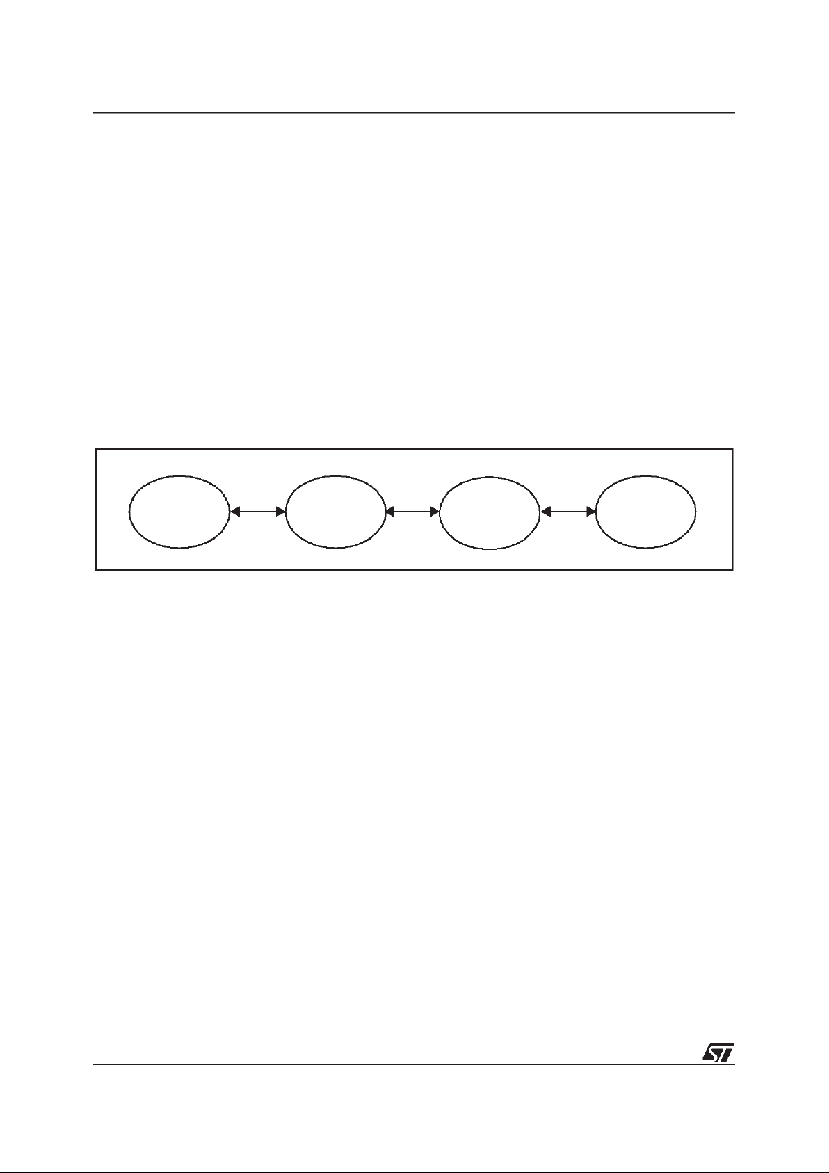
3.1 CLOCK SYSTEM
3.1.1 General Description
The MCU accepts either a crystal or ceramic resonator, or an external clock signal todrive the internal oscillator. The internal clock (f
CPU
) is derived
from the external oscillator frequency (f
OSC).
The
external Oscillator clock is first divided by 2, and
an additional divisionfactor of 2, 4, 8, or 16 canbe
applied, in Slow Mode, to reduce the frequency of
the f
CPU
; this clock signal is also routed to the on-
chip peripherals. TheCPU clock signal consists of
a squarewave with a duty cycle of 50%.
The internal oscillator is designed to operate with
an AT-cut parallel resonant quartz crystal resonator in the frequency range specified for f
osc
.The
circuit shown in Figure 11 is recommended when
using a crystal, and Table 5 lists the recommended capacitance and feedback resistance values.
The crystal and associated componentsshould be
mounted as close as possible to the input pins in
order to minimize output distortion and start-up
stabilisation time.
Use of an external CMOS oscillator is recommended when crystals outside the specified frequency ranges are to be used.
3.1.2 External Clock
An externalclock maybe applied tothe OSCIN input with the OSCOUT pin not connected, as
shown onFigure 10.
Table 5 Recommended Values for 16 MHz
Crystal Resonator (C0< 7pF)
R
SMAX
: Parasitic series resistance of the quartz
crystal (upperlimit).
C0: Parasitic shunt capacitance of the quartz crys-
tal (upper limit 7pF).
C
OSCOUT,COSCIN
: Maximum total capacitance on
pins OSCIN and OSCOUT (the valueincludes the
external capacitance tied to the pin plus the parasitic capacitance of the board and of the device).
Figure 10. External Clock Source Connections
Figure 11. Crystal/CeramicResonator
Figure 12. Clock Prescaler Block Diagram
R
SMAX
40 Ω 60 Ω 150 Ω
C
OSCIN
56pF 47pF 22pF
C
OSCOUT
56pF 47pF 22pF
OSCIN OSCOUT
EXTERNAL
CLOCK
NC
OSCIN OSCOUT
C
OSCIN
C
OSCOUT
OSCIN
OSCOUT
C
OSCIN C
OSCOUT
%2 %2,4,8, 16
f
CPU
to CPU and
Peripherals
18
19/106
ST72E331 ST72T331
3.2 RESET
3.2.1 Introduction
There are four sources of Reset:
– RESET pin (externalsource)
– Power-On Reset (Internal source)
– WATCHDOG (Internal Source)
– Low Voltage Detection Reset (internal source)
The Reset Service Routine vectoris located at ad-
dress FFFEh-FFFFh.
3.2.2 External Reset
The RESET pin is both an input and an open-drain
output with integrated pull-up resistor. When one
of the internal Reset sources is active, the Reset
pin is driven low for a duration of t
RESET
to reset
the whole application.
3.2.3 ResetOperation
The duration of the Reset state is a minimum of
4096 internal CPU Clock cycles. During the Reset
state, all I/Os take their reset value.
A Reset signal originating from an externalsource
must have a duration of at least t
PULSE
in orderto
be recognised. This detection is asynchronous
and therefore the MCUcan enter Reset state even
in Halt mode.
At the end of the Reset cycle, the MCU may be
held in the Reset state by an External Reset signal. The RESET pin may thus be used to ensure
VDDhas risen toa point where the MCU can operate correctly before the user program is run. Following a Reset event, or after exiting Halt mode, a
4096 CPU Clock cycle delay period is initiated in
order to allow the oscillator to stabilise and to ensure that recovery has taken place from theReset
state.
In the high state, the RESET pin is connected internally to a pull-up resistor (RON). This resistor
can be pulled low by external circuitry to reset the
device.
The RESET pin is an asynchronous signal which
plays a majorrole inEMS performance. In a noisy
environment, it is recommended to use the external connections shown in Figure 6.
Figure 13. Reset Block Diagram
INTERNAL
RESET
WATCHDOG RESET
OSCILLATOR
SIGNAL
COUNTER
RESET
TO ST7
RESET
POWER-ON RESET
V
DD
LOW VOLTAGE DETECTOR RESET
R
ON
19
20/106
ST72E331 ST72T331
RESET (Cont’d)
3.2.4 LowVoltage Detector Reset
The on-chip Low Voltage Detector (LVD) generates a static reset when the supply voltage is below a reference value. The LVD functions both
during power-on as well as when the power supply
drops (brown-out). The reference value for a voltage drop islower than the referencevalue for power-on in order to avoid a parasitic reset when the
MCU starts running and sinks current on the supply (hysteresis).
The LVD Reset circuitry generates a reset when
VDDis below:
V
LVDUP
when VDDis rising
V
LVDDOWN
when VDDis falling
Provided the minimun VDDvalue (guaranteed for
the oscillator frequency) is above V
LVDDOWN
, the
MCU can only be in two modes:
- underfull softwarecontrol or
- instatic safe reset
In this condition, secure operation is always en-
sured for the application without the need for external reset hardware.
During a Low Voltage Detector Reset, the RESET
pin is held low, thus permitting the MCU to reset
other devices.
In noisy environments, the power supplymay drop
for short periods and cause the Low Voltage Detector to generate a Reset too frequently. In such
cases, it is recommended to use devices without
the LVD Reset option and to rely on the watchdog
function to detect application runaway conditions.
Figure14.LowVoltage Detector ResetFunction
Figure 15. Low Voltage Detector Reset Signal
Note: See electrical characteristics for values of
V
LVDUP
and V
LVDDOWN
Figure 16. Temporization timing diagram after an internal Reset
LOW VOLTAGE
DETECTOR RESET
V
DD
FROM
WATCHDOG
RESET
RESET
RESET
V
DD
V
LVDUP
V
LVDDOWN
V
DD
Addresses
$FFFE
Temporization (4096CPU clock cycles)
V
LVDUP
20

21/106
ST72E331 ST72T331
3.3 INTERRUPTS
The ST7 coremay be interrupted by one of two different methods: maskable hardware interrupts as
listed in the Interrupt Mapping Table and a nonmaskable software interrupt (TRAP). The Interrupt
processing flowchartis shown in Figure 17.
The maskable interrupts mustbe enabled clearing
the I bitin order tobe serviced. However, disabled
interrupts may be latched and processed when
they are enabled (see external interrupts subsection).
When an interrupt has to be serviced:
– Normal processing is suspended at the end of
the current instruction execution.
– The PC, X, A and CC registersare saved onto
the stack.
– The I bit of theCC register isset to prevent addi-
tional interrupts.
– ThePC is thenloaded with the interrupt vectorof
the interrupt to service and the first instructionof
the interrupt serviceroutine is fetched (refer to
the Interrupt Mapping Table for vector addresses).
The interrupt service routine should finish with the
IRET instruction which causes the contents of the
saved registersto be recovered from thestack.
Note: As a consequence of the IRET instruction,
the I bit will be cleared and the main program will
resume.
Priority management
By default, a servicing interrupt can not be interrupted because the I bit is set by hardware entering in interrupt routine.
In the case several interrupts are simultaneously
pending, an hardware priority defines which one
will be serviced first (seethe Interrupt Mapping Table).
Non Maskable Software Interrupts
This interrupt is entered when the TRAP instruction is executed regardless of the state of theI bit.
It will be serviced according to the flowchart on
Figure 17.
Interrupts and Low power mode
All interrupts allowthe processor to leave the Wait
low power mode. Only external and specific mentioned interrupts allow the processor to leave the
Halt low power mode (refer to the “Exit from HALT“
column in the Interrupt Mapping Table).
External Interrupts
External interrupt vectorscan be loaded in the PC
register if the corresponding external interrupt occurred and if the I bit is cleared. These interrupts
allow the processor to leave the Halt low power
mode.
The external interrupt polarity is selected through
the miscellaneous register or interrupt register (if
available).
External interrupt triggered on edge will be latched
and the interrupt request automatically cleared
upon entering the interrupt service routine.
If several input pins, connected to the same interrupt vector, are configured as interrupts, their signals are logically ANDed before entering the edge/
level detection block.
Warning: The type of sensitivity defined in the
Miscellaneous or Interrupt register (if available)
applies to the EI source. In case of an ANDed
source (as described on the I/O ports section), a
low level on an I/O pin configured as input with interrupt, masks the interrupt request even in case
of rising-edge sensitivity.
Peripheral Interrupts
Different peripheral interrupt flags in the status
register are able to cause an interrupt when they
are active if both:
– TheI bit of the CC register is cleared.
– Thecorresponding enable bit is setin the control
register.
If any of these two conditions is false, the interrupt
is latched and thus remains pending.
Clearing an interrupt request is done by:
– writing “0” to the corresponding bit in the status
register or
– anaccess to the status register while the flag is
set followed bya read or write of an associated
register.
Note: the clearing sequence resets the internal
latch. A pending interrupt (i.e. waiting for being enabled) will therefore be lost if the clear sequence is
executed.
21
22/106
ST72E331 ST72T331
INTERRUPTS (Cont’d)
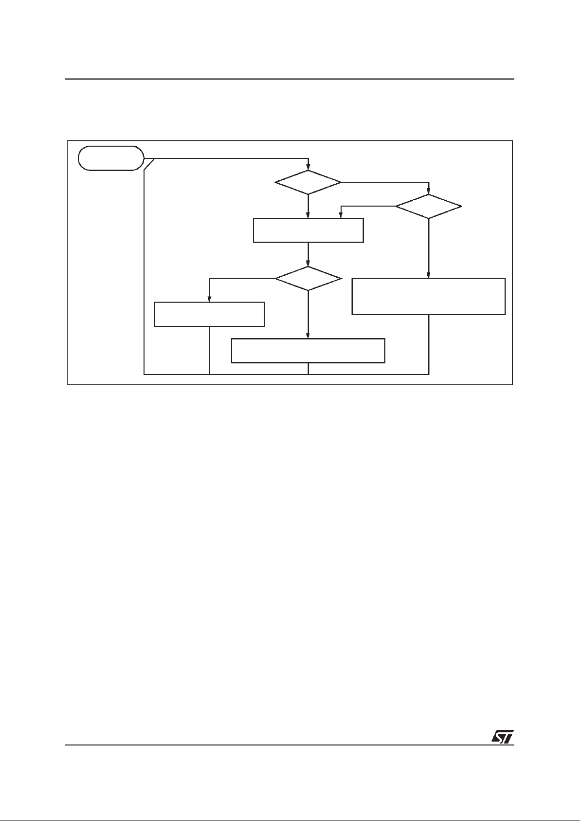
Figure 17. Interrupt Processing Flowchart
BIT I SET
Y
N
IRET
Y
N
FROM RESET
LOAD PC FROM INTERRUPT VECTOR
STACK PC, X, A, CC
SET I BIT
FETCH NEXT INSTRUCTION
EXECUTE INSTRUCTION
THIS CLEARS I BIT BY DEFAULT
RESTORE PC,X, A, CC FROM STACK
BIT I SET
Y
N
22
23/106
ST72E331 ST72T331
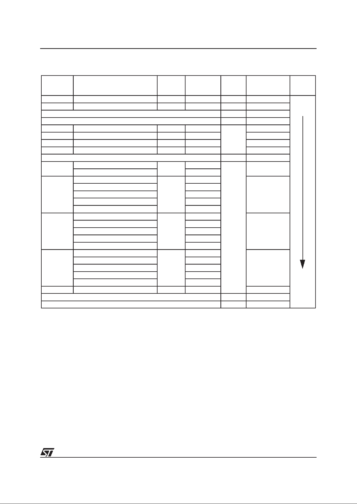
Table 6. Interrupt Mapping
Source
Block
Description
Register
Label
Flag
Exit
from
HALT
Vector
Address
Priority
Order
RESET Reset N/A N/A yes FFFEh-FFFFh
TRAP Software N/A N/A no FFFCh-FFFDh
NOT USED FFFAh-FFFBh
NOT USED FFF8h-FFF9h
EI0 Ext. Interrupt (Ports PA0:PA3) N/A N/A
yes
FFF6h-FFF7h
EI1 Ext. Interrupt (Ports PF0:PF2) N/A N/A FFF4h-FFF5h
EI2 Ext. Interrupt (Ports PB0:PB3) N/A N/A FFF2h-FFF3h
EI3 Ext. Interrupt (Ports PB4:PB7) N/A N/A FFF0h-FFF1h
NOT USED FFEEh-FFEFh
SPI
Transfer Complete
SPISR
SPIF
no
FFECh-FFEDh
Mode Fault MODF
TIMER A
Input Capture 1
TASR
ICF1_A
FFEAh-FFEBh
Output Compare 1 OCF1_A
Input Capture 2 ICF2_A
Output Compare 2 OCF2_A
Timer Overflow TOF_A
TIMER B
Input Capture 1
TBSR
ICF1_B
FFE8h-FFE9h
Output Compare 1 OCF1_B
Input Capture 2 ICF2_B
Output Compare 2 OCF2_B
Timer Overflow TOF_B
SCI
Transmit Buffer Empty
SCISR
TDRE
FFE6h-FFE7h
Transmit Complete TC
Receive Buffer Full RDRF
Idle Line Detect IDLE
Overrun OR
EEPROM EEPROM End of Programming EEPCR E2ITE FFE4h-FFE5h
NOT USED FFE2h-FFE3h
NOT USED FFE0h-FFE1h
Highest
Priority
Priority
Lowest
23
24/106
ST72E331 ST72T331
3.4 POWER SAVING MODES
3.4.1 Introduction
There are threePower Savingmodes. Slow Mode
is selected by setting the relevant bits in the Miscellaneous register. Wait and Halt modes may be
entered usingthe WFI and HALT instructions.
3.4.2 Slow Mode
In Slow mode, the oscillator frequency can be divided by a value defined in the Miscellaneous
Register. The CPU and peripherals are clocked at
this lower frequency. Slow mode isused to reduce
power consumption, andenables the userto adapt
clock frequencyto available supply voltage.
3.4.3 Wait Mode
Wait mode places the MCU in a low power consumption mode by stoppingthe CPU. Allperipherals remain active. During Wait mode, the I bit (CC
Register) is cleared, so as to enable all interrupts.
All otherregisters and memory remain unchanged.
The MCU will remain in Wait mode until an Interrupt or Reset occurs, whereupon the Program
Counter branches to the starting address of the Interrupt orReset Service Routine.
The MCU will remain in Waitmode until a Reset or
an Interrupt occurs, causing it to wake up.
Refer to Figure 18 below.
Figure 18. WAIT Flow Chart
WFI INSTRUCTION
RESET
INTERRUPT
Y
N
N
Y
CPU CLOCK
OSCILLATOR
PERIPH. CLOCK
I-BIT
ON
ON
CLEARED
OFF
Note: Before servicing an interrupt, the CC register is
pushed on the stack. The I-Bit is set during the interrupt routine and cleared when the CC register is
popped.
4096 CPU CLOCK
FETCH RESET VECTOR
OR SERVICE INTERRUPT
CYCLES DELAY
CPU CLOCK
OSCILLATOR
PERIPH. CLOCK
I-BIT
ON
ON
SET
ON
CPU CLOCK
OSCILLATOR
PERIPH. CLOCK
I-BIT
ON
ON
SET
ON
24
25/106
ST72E331 ST72T331
POWER SAVINGMODES (Cont’d)
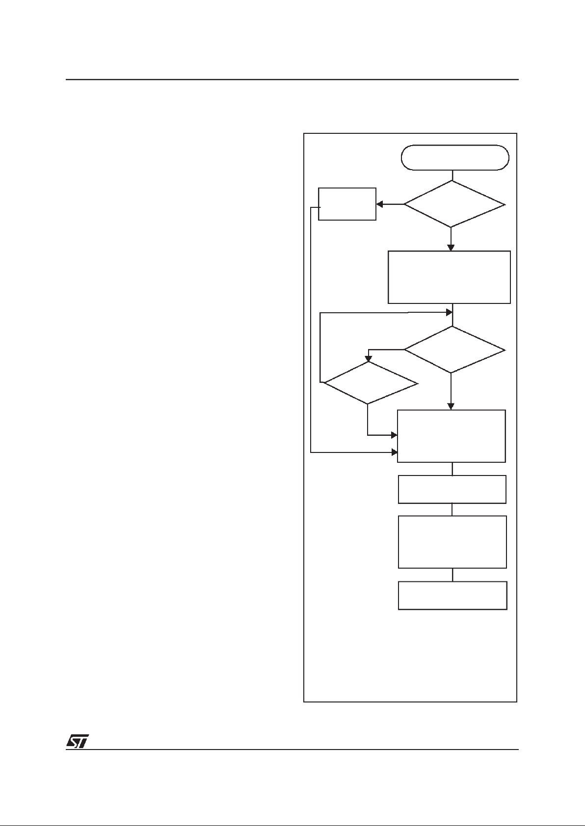
3.4.4 Halt Mode
The Halt mode is the MCU lowest power consumption mode. The Halt mode is entered by executing theHALT instruction. The internal oscillator
is then turned off, causing all internal processing to
be stopped, including the operation of the on-chip
peripherals. The Halt mode cannot be used when
the watchdog isenabled, ifthe HALT instruction is
executed while the watchdog system is enabled,a
watchdog reset is generatedthus resetting the entire MCU.
When entering Halt mode, the Ibit in the CC Register is clearedso as toenable External Interrupts.
If an interrupt occurs, the CPU becomes active.
The MCU canexit the Halt mode upon reception of
an interrupt or a reset. Refer to the Interrupt Mapping Table. The oscillator is then turned on and a
stabilization time is provided beforereleasing CPU
operation. Thestabilization timeis 4096 CPU clock
cycles.
After the start up delay, the CPU continuesoperation byservicing the interrupt whichwakes itup or
by fetching the reset vector if a reset wakes it up.
Figure 19. HALT Flow Chart
N
N
EXTERNAL
INTERRUPT
1)
RESET
HALT INSTRUCTION
4096 CPU CLOCK
FETCH RESET VECTOR
OR SERVICE INTERRUPT
CYCLES DELAY
CPU CLOCK
OSCILLATOR
PERIPH. CLOCK
2)
I-BIT
ON
OFF
SET
ON
CPU CLOCK
OSCILLATOR
PERIPH. CLOCK
I-BIT
OFF
OFF
CLEARED
OFF
Y
Y
WDG
ENABLED?
N
Y
RESET
WATCHDOG
1) or some specific interrupts
Note: Before servicing an interrupt, the CC register is
pushed on the stack. The I-Bit is set during the interrupt routine and cleared when the CC register is
popped.
CPU CLOCK
OSCILLATOR
PERIPH. CLOCK
I-BIT
ON
ON
SET
ON
2) if reset PERIPH. CLOCK = ON ; if interrupt
PERIPH. CLOCK = OFF
25
26/106
ST72E331 ST72T331
3.5 MISCELLANEOUS REGISTER
The Miscellaneous register allows to select the
SLOW operatingmode, the polarity of external interrupt requestsand to output the internal clock.
Register Address:0020h — Read/Write
Reset Value: 0000 0000 (00h)
Bit 7:6 = PEI[3:2]
External Interrupt EI3 and EI2
Polarity Options
.
These bits are set and cleared by software. They
determine which event on EI2 and EI3 causes the
external interrupt according to Table 7.
Table 7. EI2 and EI3 ExternalInterrupt Polarity
Options
Note: Any modification of one of these two bits re-
sets the interrupt request related to this interrupt
vector.
Bit 5 = MCO
Main Clock Out
This bit isset and cleared by software. Whenset, it
enables the output of the Internal Clock on the
PPF0 I/O port.
0 -PF0 is a general purposeI/O port.
1 -MCO alternate function (f
CPU
is output on PF0
pin).
Bit 4:3 = PEI[1:0]
External Interrupt EI1 and EI0
Polarity Options
.
These bits are set and cleared by software. They
determine which event on EI0 and EI1 causes the
external interrupt according to Table 8.
Table 8. EI0 and EI1 External Interrupt Polarity
Options
Note: Any modification of oneof thesetwo bitsre-
sets the interrupt request related to this interrupt
vector.
Bit 2:1 = PSM[1:0]
Prescaler forSlow Mode
These bits are set and cleared by software. They
determine the CPU clock when the SMS bit is set
according to the following table.
Table 9. f
CPU
Value in Slow Mode
Bit 0 = SMS
Slow Mode Select
This bit is set andcleared by software.
0: Normal Mode - f
CPU=fOSC
/2
(Reset state)
1: Slow Mode -the f
CPU
valueis determined bythe
PSM[1:0] bits.
70
PEI3 PEI2 MCO PEI1 PEI0 PSM1 PSM0 SMS
MODE PEI3 PEI2
Falling edge and low level
(Reset state)
00
Falling edge only 1 0
Rising edge only 0 1
Rising and falling edge 1 1
MODE PEI1 PEI0
Falling edge and low level
(Reset state)
00
Falling edge only 1 0
Rising edge only 0 1
Rising and falling edge 1 1
f
CPU
Value
PSM1 PSM0
f
OSC
/4 0 0
f
OSC
/16 0 1
f
OSC
/8 1 0
f
OSC
/32 1 1
26

27/106
ST72E331 ST72T331
4 ON-CHIP PERIPHERALS
4.1 I/O PORTS
4.1.1 Introduction
The I/O ports offer different functional modes:
– transferof datathrough digital inputs and outputs
and forspecific pins:
– analog signal input (ADC)
– alternate signal input/output for the on-chip pe-
ripherals.
– external interrupt generation
An I/O port is composed of up to 8 pins. Each pin
can be programmedindependently as digital input
(with or without interrupt generation) or digital output.
4.1.2 Functional Description
Each portis associated to 2 main registers:
– Data Register (DR)
– Data Direction Register (DDR)
and someof them to an optional register:
– Option Register(OR)
Each I/Opin may beprogrammed using thecorre-
sponding register bits in DDR and OR registers: bit
X corresponding to pin X of the port. The same correspondence is used for the DR register.
The following description takes into account the
OR register, for specific ports whichdo not provide
this register refer to the I/O Port Implementation
Section 4.1.3. The generic I/O block diagram is
shown onFigure 21.
4.1.2.1 Input Modes
The input configuration isselected by clearing the
corresponding DDRregister bit.
In this case, reading the DR register returns the
digital value applied to the external I/O pin.
Different input modes can be selected by software
through theOR register.
Notes:
1. All the inputs are triggered by a Schmitt trigger.
2. When switching from input mode to output
mode, the DR register should be written first to
output the correct value as soon as the port is configured as an output.
Interrupt function
When an I/O is configured in Input with Interrupt,
an event on this I/O can generate an external Interrupt request to the CPU. The interrupt polarity is
given independently according to the description
mentioned in the Miscellaneous register or in the
interrupt register (where available).
Each pin can independently generate an Interrupt
request.
Each external interrupt vector is linked to a dedicated group of I/O port pins (see Interrupts section). If several input pins are configured as inputs
to the same interrupt vector, their signals are logically ANDed before entering the edge/level detection block. For this reason if one of the interrupt
pins is tied low, it masks the other ones.
4.1.2.2 Output Mode
The pin is configured in output modeby setting the
corresponding DDR registerbit.
In this mode, writing “0” or “1” to the DR register
applies this digital value to the I/O pin through the
latch. Then reading the DR register returns the
previously stored value.
Note: In this mode, the interrupt function is disabled.
4.1.2.3 Digital Alternate Function
When an on-chipperipheral is configured to use a
pin, the alternate function is automatically selected. This alternate function takes priority over
standard I/O programming. When the signal is
coming from an on-chip peripheral, the I/O pin is
automatically configuredin output mode (push-pull
or open drain according to the peripheral).
When the signal is going to an on-chip peripheral,
the I/O pin has to be configured ininput mode. In
this case, the pin’s state is also digitally readable
by addressing the DR register.
Notes:
1. Input pull-up configuration can cause an unexpected value atthe input of the alternate peripheral input.
2. When the on-chip peripheral uses apin asinput
and output, this pin must be configured asan input
(DDR = 0).
Warning
: The alternate function must not be acti-
vated as long as the pin isconfigured as input with
interrupt, in order to avoid generating spurious interrupts.
27
28/106
ST72E331 ST72T331
I/O PORTS (Cont’d)
4.1.2.4 Analog Alternate Function
When the pin isused asan ADC input theI/O must
be configured as input, floating. The analog multiplexer (controlled by the ADC registers) switches
the analog voltage present on the selected pin to
the common analog rail which is connected to the
ADC input.
It isrecommended not to change the voltage level
or loading on any port pin while conversion is in
progress. Furthermore it is recommended not to
have clocking pins located close to a selected analog pin.
Warning
: The analog input voltage level must be
within the limits stated in the Absolute Maximum
Ratings.
4.1.3 I/O Port Implementation
The hardware implementation oneach I/O port depends on the settingsin the DDR andOR registers
and specific feature of the I/O portsuch as ADCInput (see Figure 21) or true open drain. Switching
these I/O ports from one state to another should
be done in a sequence that prevents unwanted
side effects. Recommended safetransitions are illustrated in Figure 20. Other transitions are potentially risky and should be avoided, since they are
likely to present unwanted side-effects such as
spurious interrupt generation.
Figure 20. Recommended I/O State Transition Diagram
with interrupt
INPUT
OUTPUT
no interrupt
INPUT
push-pullopen-drain
OUTPUT
28
29/106
ST72E331 ST72T331
I/O PORTS (Cont’d)
Figure 21. I/O BlockDiagram
Table 10. Port Mode Configuration
Legend:
0 - present, not activated
1 - present and activated
Notes:
– No OR Register on some ports (see register map).
– ADC Switch on ports with analog alternate functions.
DR
DDR
LATCH
LATCH
DATA BUS
DR SEL
DDR SEL
V
DD
PAD
ANALOG
SWITCH
ANALOG ENABLE
(ADC)
M
U
X
ALTERNATE
ALTERNATE
ALTERNATE ENABLE
COMMON ANALOG RAIL
ALTERNATE
M
U
X
ALTERNATE INPUT
PULL-UP
OUTPUT
P-BUFFER
(S
EE TABLE BELOW)
N-BUFFER
1
0
1
0
OR
LATCH
ORSEL
FROM
OTHER
BITS
EXTERNAL
PULL-UP
CONDITION
ENABLE
ENABLE
GND
(S
EE TABLE BELOW)
(S
EE NOTE BELOW)
CMOS
SCHMITT TRIGGER
SOURCE (EIx)
INTERRUPT
POLARITY
SEL
GND
V
DD
DIODE
(SEE TABLEBELOW)
Configuration Mode Pull-up P-buffer V
DD
Diode
Floating 0 0 1
Pull-up 1 0 1
Push-pull 0 1 1
True Open Drain not present not present not present
Open Drain (logic level) 0 0 1
29

30/106
ST72E331 ST72T331
I/O PORTS (Cont’d)
Table 11. Port Configuration
Notes:
1. ST72T331N only
2. For OTP/EPROM version, when OR=0: floating & when OR=1: reserved
3. For OTP/EPROM version, when OR=0: open-drain, high sink capability & when OR=1: reserved
* Reset state (The bits corresponding to unavailable pins are forced to 1 by hardware, this affects thereset status value).
Warning: All bits of the DDR register which correspond to unconnected I/Os must be left at their reset value. They must
not be modified by the user otherwise a spurious interrupt may be generated.
Port Pin name
Input (DDR = 0) Output (DDR = 1)
OR= 0 OR= 1 OR = 0 OR =1
Port A
PA0:PA2
1)
floating* pull-up with interrupt open-drain push-pull
PA3 floating* pull-up with interrupt open-drain push-pull
PA4:PA7 floating* open drain, high sink capability
Port B
PB0:PB4 floating* pull-up with interrupt open-drain
push-pull
PB5:PB7
1)
floating* pull-up with interrupt open-drain
push-pull
Port C PC0:PC7 floating* pull-up open-drain push-pull
Port D
PD0:PD5 floating* pull-up open-drain push-pull
PD6:PD7
1)
floating* pull-up open-drain push-pull
Port E
PE0:PE1 floating* pull-up open-drain push-pull
PE4:PE7
1)
floating*
2)
open drain, high sink capability
3)
Port F
PF0:PF2 floating* pull-up with interrupt open-drain push-pull
PF4, PF6,PF7 floating* pull-up open-drain push-pull
30

31/106
ST72E331 ST72T331
I/O PORTS (Cont’d)
4.1.4 Register Description
4.1.4.1 Data registers
Port A Data Register (PADR)
Port B Data Register (PBDR)
Port C Data Register (PCDR)
Port D Data Register (PDDR)
Port E Data Register (PEDR)
Port F Data Register (PFDR)
Read/Write
Reset Value: 0000 0000 (00h)
Bit 7:0 = D7-D0
Data Register 8 bits.
The DR register has a specific behaviour according to the selected input/output configuration. Writing the DR register is always taken in account
even if the pin is configured as an input. Reading
the DR register returns either theDR register latch
content (pin configuredas output) or the digital value applied to the I/O pin (pin configured as input).
4.1.4.2 Data direction registers
Port A Data Direction Register (PADDR)
Port B Data Direction Register (PBDDR)
Port C Data Direction Register (PCDDR)
Port D Data Direction Register (PDDDR)
Port E Data Direction Register (PEDDR)
Port F Data Direction Register (PFDDR)
Read/Write
Reset Value: 0000 0000 (00h) (input mode)
Bit 7:0 = DD7-DD0
Data Direction Register 8 bits.
The DDR register gives the input/output direction
configuration of the pins. Each bits is set and
cleared by software.
0: Input mode
1: Output mode
4.1.4.3 Option registers
Port A OptionRegister (PAOR)
Port B OptionRegister (PBOR)
Port C Option Register (PBOR)
Port D Option Register (PBOR)
Port E OptionRegister (PBOR)
Port F Option Register (PFOR)
Read/Write
Reset Value: see Register Memory Map Table 4
Bit 7:0 = O7-O0
Option Register8 bits.
The OR register allow to distinguish in input mode
if the interrupt capability or the floating configuration is selected.
In output mode it select push-pull or open-drain
capability.
Each bit is set and clearedby software.
Input mode:
0: floating input
1: input pull-up with interrupt
Output mode:
0: open-drain configuration
1: push-pull configuration
70
D7 D6 D5 D4 D3 D2 D1 D0
70
DD7 DD6 DD5 DD4 DD3 DD2 DD1 DD0
70
O7 O6 O5 O4 O3 O2 O1 O0
31

32/106
ST72E331 ST72T331
I/O PORTS (Cont’d)
Table 12. I/O Port RegisterMap
Address
(Hex.)
Register
Label
76543210
0000h PADR D7 D6 D5 D4 D3 D2 D1 D0
0001h PADDR DD7 DD6 DD5 DD4 DD3 DD2 DD1 DD0
0002h PAOR O7 O6 O5 O4 O3 O2 O1 O0
0004h PCDR D7 D6 D5 D4 D3 D2 D1 D0
0005h PCDDR DD7 DD6 DD5 DD4 DD3 DD2 DD1 DD0
0006h PCOR O7 O6 O5 O4 O3 O2 O1 O0
0008h PBDR D7 D6 D5 D4 D3 D2 D1 D0
0009h PBDDR DD7 DD6 DD5 DD4 DD3 DD2 DD1 DD0
000Ah PBOR O7 O6 O5 O4 O3 O2 O1 O0
000Ch PEDR D7 D6 D5 D4 D3 D2 D1 D0
000Dh PEDDR DD7 DD6 DD5 DD4 DD3 DD2 DD1 DD0
000Eh PEOR O7 O6 O5 O4 O3 O2 O1 O0
0010h PDDR D7 D6 D5 D4 D3 D2 D1 D0
0011h PDDDR DD7 DD6 DD5 DD4 DD3 DD2 DD1 DD0
0012h PDOR O7 O6 O5 O4 O3 O2 O1 O0
0014h PFDR D7 D6 D5 D4 D3 D2 D1 D0
0015h PFDDR DD7 DD6 DD5 DD4 DD3 DD2 DD1 DD0
0016h PFOR O7 O6 O5 O4 O3 O2 O1 O0
32

33/106
ST72E331 ST72T331
4.2 EEPROM (EEP)
4.2.1 Introduction
The Electrically Erasable Programmable Read
Only Memory is used to storedata that need a non
volatile back-up. The use ofthe EEPROM requires
a basic protocol described in this chapter.
4.2.2 Main Features
■ Up to 16 bytes programmed in the same cycle
■ EEPROM mono-voltage (charge pump)
■ Chained erase and programming cycles
■ Internal control ofthe globalprogramming cycle
duration
■ End of programming cycle interrupt flag
■ WAIT mode management
Figure 22. EEPROM Block Diagram
BUFFER
ROW
DECODER
16*8 BITS
DATA LATCHES
DATA
MULTIPLEXER
HIGH VOLTAGEPUMP
EEPROM
MEMORY
MATRIX
1 ROW = 16 *8 BITS
ADDRESS
DECODER
ADDRESS
BUS
DATA
BUS
E2ITE E2LAT E2PGM
EEPCR
RESERVED
.
.
.
.
.
.
128
128
8
8
4
4
12
INTERRUPT
REQUEST
FALLING
EDGE
DETECTOR
33

34/106
ST72E331 ST72T331
EEPROM (Cont’d)
4.2.3 Functional description
4.2.3.1 Read operation (E2LAT=0)
The EEPROM can be read asa normal ROM location when the E2LAT bit of the CR register is
cleared. In a read cycle, the desired byte is put on
the data bus in less than 1 CPU clock cycle. This
means that reading data from EEPROM takes the
same time as reading data from EPROM, but this
memory cannot be usedto execute machine code.
4.2.3.2 Write operation (E2LAT=1)
The EEPROM programming flowchart is shown in
Figure 24.
To access write mode set the E2LAT bit, the
E2PGM bit stays cleared. Then when a write access to the EEPROM occurs, the value onthe data
bus is latched on the 16 data latches depending
on the address.
When E2PGM is set, all the previous bytes written
(1 up to 16) are programmed in the EEPROM
cells. The effective high address (row) is determined by the last EEPROM write sequence. To
avoid wrong programming, the user must take
care that all the bytes written between two pro-
gramming sequences have the same high address: onlythe four Least SignificantBits of the address can change.
At the end of the cycle, the E2PGM and E2LAT
bits are cleared simultaneously,and aninterrupt is
generated if theE2ITE bit is set.
Note: Care should be taken during the programming cycle. Writing to the same memory location
will over-program the memory (logical AND between the two write access data result) because
the data latches are only cleared at the end of the
programming cycle and by the falling edge of
E2LAT bit.
It is not possible to read the latched data.
4.2.3.3 EEPROM Access Error handling
If a read access occurs while E2LAT=1, then the
data bus will not be driven.
If a write access occurs while E2LAT=0, then the
data on the bus will not be latched.
If a programming cycleis interrupted(by software/
RESET action), the memory data will not be guaranteed.
34

35/106
ST72E331 ST72T331
EEPROM (Cont’d)
Figure 23. EEPROM ProgrammingCycle
Figure 24. EEPROM ProgrammingFlowchart
Erase cycle
Write cycle
Tprog
Read operation allowed
Read operation not possible
INTERNAL
PROGRAMMING
VOLTAGE
Write of
data
latches
E2LAT
E2PGM
INTERRUPT
REQUEST
Interrupt
vector fetch
E2LAT=1
E2PGM=0
(Write mode)
Write bytes in
EEPROM
E2LAT=1
E2PGM=1
(Start
programming
cycle)
Wait for endof
programming
(E2LAT=0
or interrupt)
Write 1 to 16bytes
in the same row
(with the same 12
Most Significant
Bits of the address)
E2LAT=0
E2PGM=0
(Read mode)
35

36/106
ST72E331 ST72T331
EEPROM (Cont’d)
4.2.4 LowPower Modes
4.2.5 Interrupts
Note: This event generates an interrupt if the corresponding Enable Control Bit is set and the I-bit in the
CC registeris reset (RIM instruction).
4.2.6 Register Description
EEPROM CONTROL REGISTER (CR)
Read/Write
Reset Value: 0000 0000 (00h)
Bit 7:3= Reserved, forced by hardware to 0.
Bit 2 = E2ITE:
Interrupt enable.
Thisbitisset andclearedbysoftware. Itenablesthe
Data EEPROM interrupt capability when the
E2PGM bitis cleared byhardware.Theinterruptrequest is automatically cleared when the software
enters the interrupt routine.
0: Interrupt disabled
1: Interrupt enabled
Bit 1 = E2LAT:
Read/Write mode.
This bit is set by software. It is cleared by hardware at the end of the programming cycle. It can
only be cleared by software if E2PGM=0.
0: Read mode
1: Write mode
Bit 0 = E2PGM:
Programming Control.
This bit is set by software to begin the programming cycle. At the end of the programming cycle,
this bit is cleared by hardware and an interrupt is
generated if theE2ITE bit is set.
0: Programming finished or not started
1: Programming cycle is in progress
Note: if the E2PGM bit is cleared during the programming cycle, the memory data is not guaranteed.
Mode Description
WAIT
The EEPROM can enter WAIT mode on execution of theWFI instruction of the microcontroller.
The EEPROM will immediately enter this mode if there is no programming in progress, otherwise the EEPROM will finish the cycle and then enter WAIT mode.
The EEPROM interrupt exits from Wait mode.
HALT
The EEPROM immediately enters HALT mode if the microcontroller executes the HALT instruction. Therefore the EEPROM will stop the function in progress, and data may be corrupted.
Interrupt Event
Event
Flag
Enable
Control
Bit
Exit
from
Wait
Exit
from
Halt
End of Programming Cycle E2PGM E2ITE Yes No
70
0 0 0 0 0 E2ITE E2LAT E2PGM
36

37/106
ST72E331 ST72T331
4.3 WATCHDOG TIMER (WDG)
4.3.1 Introduction
The Watchdog timer is used to detect the occurrence of a software fault, usually generated by external interference or by unforeseen logical conditions, which causes the application program to
abandon its normal sequence. The Watchdog circuit generates an MCU reset on expiry of a programmed time period, unless theprogram refreshes the counter’s contents before the T6 bit becomes cleared.
4.3.2 Main Features
■ Programmable timer (64 increments of 12288
CPU cycles)
■ Programmable reset
■ Reset (if watchdog activated) after a HALT
instruction or when the T6 bit reaches zero
■ Hardware Watchdog selectable by optionbyte
■ Watchdog Reset indicated by status flag (in
versions with Safe Reset option only)
4.3.3 Functional Description
The counter value stored in the CR register (bits
T[6:0]), is decremented every 12,288 machine cycles, and the length of the timeout period can be
programmed by the user in 64 increments.
If the watchdog is activated (the WDGA bit is set)
and when the 7-bit timer (bits T[6:0]) rolls over
from 40h to 3Fh (T6 becomes cleared), it initiates
a reset cycle pulling low the reset pin for typically
500ns.
Figure 25. Watchdog Block Diagram
RESET
WDGA
7-BIT DOWNCOUNTER
f
CPU
T6 T0
CLOCK DIVIDER
WATCHDOG CONTROL REGISTER (CR)
÷12288
T1
T2
T3
T4
T5
37

38/106
ST72E331 ST72T331
WATCHDOG TIMER (Cont’d)
The application program must write in the CR register at regular intervals during normal operation to
prevent an MCU reset. The value to be stored in
the CR register must be between FFh and C0h
(see Table 13):
– The WDGA bit is set (watchdog enabled)
– The T6 bit is set to prevent generating an imme-
diate reset
– TheT[5:0] bits containthe number of increments
which represents the time delay before the
watchdog produces areset.
Table 13.Watchdog Timing (f
CPU
= 8 MHz)
Notes: Following a reset, the watchdog is disa-
bled. Onceactivated it cannot be disabled,except
by areset.
The T6 bit can be used to generate a software reset (the WDGA bitis set and the T6 bitis cleared).
If the watchdog is activated, the HALT instruction
will generate a Reset.
4.3.4 Hardware Watchdog Option
If Hardware Watchdog Is selected by option byte,
the watchdog is always active and the WDGA bit in
the CR is not used.
Refer to the device-specific Option Byte description.
4.3.5 LowPower Modes
4.3.6 Interrupts
None.
4.3.7 Register Description
CONTROL REGISTER (CR)
Read/Write
Reset Value: 0111 1111 (7Fh)
Bit 7 = WDGA
Activation bit
.
This bit is set by software and only cleared by
hardware after a reset. When WDGA = 1, the
watchdog can generatea reset.
0: Watchdog disabled
1: Watchdog enabled
Note: This bit is not used if the hardware watchdog option is enabled by option byte.
Bit 6:0 = T[6:0]
7-bit timer (MSB to LSB).
These bits contain the decremented value. A reset
is produced when it rolls overfrom 40h to 3Fh (T6
becomes cleared).
STATUS REGISTER (SR)
Read/Write
Reset Value*: 0000 0000 (00h)
Bit 0 = WDOGF
Watchdog flag
.
This bit is set by a watchdog reset and cleared by
software or a power on/off reset. This bit is useful
for distinguishing power/on off or external reset
and watchdog reset.
0: No Watchdog reset occurred
1: Watchdog reset occurred
* Only by software and power on/off reset
Note: This register is not used in versions without
LVD Reset.
CR Register
initial value
WDG timeout period
(ms)
Max FFh 98.304
Min C0h 1.536
Mode Description
WAIT No effect on Watchdog.
HALT
Immediate resetgeneration as soon as
the HALT instruction is executed if the
Watchdog is activated (WDGA bit is
set).
70
WDGA T6 T5 T4 T3 T2 T1 T0
70
- - - - - - - WDOGF
38

39/106
ST72E331 ST72T331
Table 14. Watchdog Timer Register Map and Reset Values
Address
(Hex.)
Register
Label
76543210
2A
WDGCR
Reset Value
WDGA
0
T6
1
T5
1
T4
1
T3
1
T2
1
T1
1
T0
1
2B
WDGSR
Reset Value
-
0
-
0
-
0
-
0
-
0
-
0
-
0
WDOGF
0
39

40/106
ST72E331 ST72T331
4.4 16-BIT TIMER
4.4.1 Introduction
The timer consists of a 16-bit free-running counter
driven by a programmable prescaler.
It may be used for a variety of purposes, including
pulse length measurement of up to two input signals (
input capture
) orgeneration of upto two out-
put waveforms (
output compare
and
PWM
).
Pulse lengths and waveform periods can be modulated from a few microseconds to several milliseconds using the timer prescaler and the CPU
clock prescaler.
4.4.2 Main Features
■ Programmableprescaler:f
CPU
dividedby2, 4or8.
■ Overflow statusflag and maskable interrupt
■ External clock input (must be at least 4 times
slower thantheCPUclock speed)with thechoice
of activeedge
■ Output compare functions with
– 2 dedicated 16-bitregisters
– 2 dedicated programmablesignals
– 2 dedicated statusflags
– 1 dedicated maskableinterrupt
■ Input capturefunctions with
– 2 dedicated 16-bitregisters
– 2 dedicated active edge selection signals
– 2 dedicated statusflags
– 1 dedicated maskableinterrupt
■ Pulse widthmodulation mode (PWM)
■ One pulse mode
■ 5 alternatefunctionson I/Oports (ICAP1,ICAP2,
OCMP1, OCMP2, EXTCLK)*
The Block Diagram is shown in Figure 26.
*Note: Some external pins are not available on all
devices. Refer to the device pin outdescription.
When reading an input signal which is not availa-
ble on an external pin, the value will always be ‘1’.
4.4.3 Functional Description
4.4.3.1 Counter
The principal block of the Programmable Timer is
a 16-bit free running increasing counter and itsassociated 16-bit registers:
Counter Registers
– Counter High Register (CHR) isthe most sig-
nificant byte (MSB).
– Counter Low Register (CLR) is the least sig-
nificant byte (LSB).
Alternate Counter Registers
– AlternateCounter High Register (ACHR)is the
most significant byte(MSB).
– AlternateCounter Low Register (ACLR) is the
least significant byte (LSB).
These two read-only 16-bit registers contain the
same value but with the differencethat reading the
ACLR register doesnot clear the TOF bit (overflow
flag), (see note at the end of paragraph titled16-bit
read sequence).
Writing in the CLR register or ACLR register resets
the free running counter to the FFFCh value.
The timer clock depends on the clock control bits
of the CR2 register, as illustratedin Table 15. The
value in the counter register repeats every
131.072, 262.144 or 524.288 internal processorclock cycles depending on the CC1 and CC0bits.
40

41/106
ST72E331 ST72T331
16-BIT TIMER (Cont’d)
Figure 26. Timer Block Diagram
MCU-PERIPHERAL INTERFACE
COUNTER
ALTERNATE
REGISTER
OUTPUT
COMPARE
REGISTER
OUTPUT COMPARE
EDGE DETECT
OVERFLOW
DETECT
CIRCUIT
1/2
1/4
1/8
8-bit
buffer
ST7 INTERNAL BUS
LATCH1
OCMP1
ICAP1
EXTCLK
f
CPU
TIMER INTERRUPT
ICF2ICF1 000OCF2OCF1 TOF
PWMOC1E EXEDGIEDG2CC0CC1
OC2E
OPMFOLV2ICIE OLVL1IEDG1OLVL2FOLV1OCIE TOIE
ICAP2
LATCH2
OCMP2
8
8
8 low
16
8 high
16 16
16
16
CR1
CR2
SR
6
16
888
888
high
low
high
high
high
low
low
low
EXEDG
TIMER INTERNAL BUS
CIRCUIT1
EDGE DETECT
CIRCUIT2
CIRCUIT
1
OUTPUT
COMPARE
REGISTER
2
INPUT
CAPTURE
REGISTER
1
INPUT
CAPTURE
REGISTER
2
CC1 CC0
16 BIT
FREE RUNNING
COUNTER
41

42/106
ST72E331 ST72T331
16-BIT TIMER (Cont’d)
16-bit read sequence: (from either the Counter
Register orthe Alternate Counter Register).
The user must read the MSB first, then the LSB
value isbuffered automatically.
This buffered value remains unchanged until the
16-bit read sequence is completed, even if the
user readsthe MSB several times.
After a complete reading sequence, if only the
CLR register or ACLR register are read, they return the LSB of the count value at the time of the
read.
Whatever the timer mode used (input capture, output compare, one pulse mode or PWM mode) an
overflow occurs when the counter rolls over from
FFFFh to0000h then:
– The TOF bitof the SR register is set.
– A timer interrupt is generated if:
– TOIE bit of the CR1 registeris set and
– I bit ofthe CC register is cleared.
If one of these conditions is false, the interrupt remains pending to be issued as soon as they are
both true.
Clearing the overflow interrupt request is done in
two steps:
1.Reading the SRregister while the TOF bit is set.
2.An access (read or write)to the CLR register.
Notes: The TOF bit is not cleared by accesses to
ACLR register. This feature allows simultaneous
use of the overflow function and reads of the free
running counter at random times (for example, to
measure elapsed time) without the risk ofclearing
the TOF biterroneously.
The timer is not affected byWAIT mode.
In HALT mode, the counter stops countinguntil the
mode is exited. Counting then resumes from the
previous count(MCU awakened by an interrupt) or
from the reset count (MCU awakened by aReset).
4.4.3.2 External Clock
The external clock (where available) is selected if
CC0=1 and CC1=1 in CR2 register.
The status of the EXEDG bit determines the type
of level transition on the external clock pin EXTCLK that willtrigger the free running counter.
The counter is synchronised with the falling edge
of the internal CPU clock.
At least four falling edges of the CPU clock must
occur between two consecutive active edges of
the external clock; thus the external clock frequency must be less than a quarter of the CPU clock
frequency.
LSB is buffered
Read MSB
At t0
Read LSB
Returns the buffered
LSB value at t0
At t0 +∆t
Other
instructions
Beginning of the sequence
Sequence completed
42

43/106
ST72E331 ST72T331
16-BIT TIMER (Cont’d)
Figure 27. Counter Timing Diagram, internal clock dividedby 2
Figure 28. Counter Timing Diagram, internal clock dividedby 4
Figure 29. Counter Timing Diagram, internal clock dividedby 8
CPU CLOCK
FFFD FFFE FFFF 0000 0001 0002 0003
INTERNAL RESET
TIMER CLOCK
COUNTER REGISTER
OVERFLOW FLAG TOF
FFFC FFFD 0000 0001
CPU CLOCK
INTERNAL RESET
TIMERCLOCK
COUNTER REGISTER
OVERFLOW FLAG TOF
CPU CLOCK
INTERNAL RESET
TIMER CLOCK
COUNTER REGISTER
OVERFLOW FLAG TOF
FFFC FFFD
0000
43

44/106
ST72E331 ST72T331
16-BIT TIMER (Cont’d)
4.4.3.3 Input Capture
In this section, the index,i, may be 1 or 2.
The two input capture 16-bit registers (IC1R and
IC2R) are used to latch the value of the free running counter after a transition detected by the
ICAPipin (see figure 5).
ICiregister is a read-only register.
The active transition is software programmable
through theIEDGibitof the ControlRegister (CRi).
Timing resolution is one count of the free running
counter: (f
CPU
/(CC1.CC0)).
Procedure:
To use the input capturefunction select the following in the CR2 register:
– Select the timer clock (CC1-CC0) (see Table
15).
– Select the edge of the active transition on the
ICAP2 pin with the IEDG2 bit (the ICAP2 pin
must be configured as floating input).
And selectthe followingin the CR1 register:
– Set the ICIE bit to generate an interruptafter an
input capture coming from both the ICAP1 pin or
the ICAP2 pin
– Select the edge of the active transition on the
ICAP1 pin with theIEDG1 bit(the ICAP1pin must
be configured as floating input).
When an input capture occurs:
– ICFibit is set.
– The ICiR register contains the value of the free
running counter on the active transition on the
ICAPipin (seeFigure 31).
– Atimer interrupt is generated ifthe ICIE bit is set
and theI bit is cleared in the CC register. Otherwise, the interrupt remains pending until both
conditions become true.
Clearing the Input Capture interrupt request is
done in two steps:
1.Reading theSR register while the ICFibitis set.
2.An access (read or write) to the ICiLR register.
Notes:
1.After reading the ICiHR register, transfer of
input capture data is inhibited until the ICiLR
register is also read.
2.The ICiR register always contains the free running counter value which corresponds to the
most recentinput capture.
3.The 2 input capture functions can be used
together even if the timer also uses the output
compare mode.
4.In One pulse Mode and PWM mode only the
input capture 2 can be used.
5.The alternate inputs (ICAP1 & ICAP2) are
always directly connected to the timer. So any
transitions on these pins activate the input capture process.
6.Moreover if one of the ICAPipin is configured
as an input and the second one as an output,
an interrupt can be generated if the user toggle
the output pin and if the ICIE bit isset.
7.The TOF bit can be used with interrupt in order
to measure event that go beyond the timer
range (FFFFh).
MS Byte LS Byte
ICiR IC
i
HR ICiLR
44

45/106
ST72E331 ST72T331
16-BIT TIMER (Cont’d)
Figure 30. Input Capture Block Diagram
Figure 31. Input Capture Timing Diagram
ICIE
CC0
CC1
16-BIT FREE RUNNING
COUNTER
IEDG1
(Control Register 1) CR1
(Control Register 2) CR2
ICF2ICF1 000
(Status Register) SR
IEDG2
ICAP1
ICAP2
EDGE DETECT
CIRCUIT2
16-BIT
IC1R RegisterIC2R Register
EDGE DETECT
CIRCUIT1
pin
pin
FF01 FF02 FF03
FF03
TIMER CLOCK
COUNTER REGISTER
ICAPi PIN
ICAPi FLAG
ICAPi REGISTER
Note: A
ctive edge is rising edge.
45

46/106
ST72E331 ST72T331
16-BIT TIMER (Cont’d)
4.4.3.4 Output Compare
In this section, the index,i, may be 1 or 2.
This function can be used to control an output
waveform or indicating when a period of time has
elapsed.
When a match is found between the Output Compare register and the freerunning counter, the output compare function:
– Assigns pins with a programmable valueif the
OCIE bit is set
– Sets a flag in the status register
– Generates an interrupt if enabled
Two 16-bit registers Output Compare Register 1
(OC1R) and Output Compare Register 2 (OC2R)
contain the value to be compared to the free running counter each timer clock cycle.
These registers are readable and writable and are
not affected by the timer hardware. A reset event
changes the OCiR valueto 8000h.
Timing resolution is one count of the free running
counter: (f
CPU/(CC1.CC0)
).
Procedure:
To use the outputcompare function, selectthe following in the CR2 register:
– Set the OCiE bit if an output is needed then the
OCMPipin is dedicated to the output compare
i
function.
– Select the timer clock (CC1-CC0) (see Table
15).
And selectthe followingin the CR1 register:
– Select theOLVLibitto appliedto the OCMPipins
after the matchoccurs.
– Set the OCIE bit to generate an interrupt if it is
needed.
When a match is found:
– OCFibit is set.
– The OCMPipin takes OLVLibit value (OCMP
i
pin latch is forced low during reset and stays low
until valid compares change it to a high level).
– A timer interrupt is generated if the OCIE bit is
set in the CR2 register and the I bit iscleared in
the CC register (CC).
The OCiR register valuerequired for a specifictim-
ing application can be calculated using thefollowing formula:
Where:
∆t = Desired output compare period (in sec-
onds)
f
CPU
= Internal clock frequency
PRESC
= Timer prescaler factor (2, 4 or 8 de-
pending on CC1-CC0 bits, see Table
15)
Clearing the output compare interrupt request is
done by:
1.Reading the SR register while the OCFibit is
set.
2.An access (read or write)to theOCiLR register.
The following procedure is recommended to prevent the OCFibit from being set between the time
it is read and the write to the OCiR register:
– Writeto the OCiHR register (further compares
are inhibited).
– Readthe SR register (first step of theclearance
of the OCFibit, which may be already set).
– Writeto the OCiLR register (enablesthe output
compare functionand clears the OCFibit).
Notes:
1.After a processor write cycle to the OCiHR register, the output compare function is inhibited
until theOCiLR register is also written.
2.If the OCiE bit is not set, the OCMPipin is a
general I/O port and the OLVLibit will not
appear when a match is found but an interrupt
could be generated if the OCIE bit is set.
3.When the clock is divided by 2, OCFiand
OCMPiare set while the counter value equals
the OCiR register value (see Figure 33, on
page 47). This behaviour is the same in OPM
or PWM mode.
When the clock is divided by 4, 8 or in external
clock mode, OCFiand OCMPiare set while the
counter value equals the OCiR register value
plus 1(see Figure 34, on page 47).
4.The outputcompare functionscan be used both
for generating external events on the OCMP
i
pins even if the input capture mode is also
used.
5.The value in the 16-bit OCiR register and the
OLVibit should be changed after each successful comparisonin orderto controlan output
waveform orestablish a new elapsed timeout.
MS Byte LS Byte
OC
i
ROC
i
HR OCiLR
∆OC
i
R=
∆t*f
CPU
PRESC
46

47/106
ST72E331 ST72T331
16-BIT TIMER (Cont’d)
Figure 32. Output Compare BlockDiagram
Figure 33. Output Compare Timing Diagram, Internal Clock Divided by 2
Figure 34. Output Compare Timing Diagram, Internal Clock Divided by 4
OUTPUT COMPARE
16-bit
CIRCUIT
OC1R Register
16 BIT FREE RUNNING
COUNTER
OC1E CC0CC1
OC2E
OLVL1OLVL2OCIE
(Control Register 1) CR1
(Control Register 2) CR2
000OCF2OCF1
(Status Register) SR
16-bit
16-bit
OCMP1
OCMP2
Latch
1
Latch
2
OC2R Register
Pin
Pin
INTERNAL CPU CLOCK
TIMER CLOCK
COUNTER
OUTPUT COMPARE REGISTER
OUTPUT COMPARE FLAG (OCFi)
OCMPi PIN (OLVLi=1)
2ED3
2ED0 2ED1 2ED2
2ED3
2ED42ECF
INTERNAL CPU CLOCK
TIMER CLOCK
COUNTER
OUTPUT COMPARE REGISTER
COMPARE REGISTER LATCH
OCFi AND OCMPi PIN (OLVLi=1)
2ED3
2ED0 2ED1 2ED2
2ED3
2ED42ECF
47

48/106
ST72E331 ST72T331
16-BIT TIMER (Cont’d)
4.4.3.5 Forced Compare
In this sectionimay represent 1 or 2.
The following bits of the CR1 register are used:
When the FOLVibit is set by software, the OLVL
i
bit iscopied to the OCMPipin. The OLVibithas to
be toggled in order to togglethe OCMPipin when
it is enabled (OCiE bit=1). The OCFibitis then not
set by hardware, and thus no interrupt request is
generated.
FOLVLibitshave no effect in both one pulse mode
and PWMmode.
4.4.3.6 One Pulse Mode
One Pulse mode enables the generation of a
pulse when an external event occurs. This mode is
selected viathe OPMbit in the CR2 register.
The one pulse mode uses the Input Capture1
function and the Output Compare1 function.
Procedure:
To useone pulse mode:
1. Load the OC1R register with the value corresponding to the length of the pulse (see the formula inSection 4.4.3.7).
2. Select the following in the CR1 register:
– Using the OLVL1 bit, select the levelto be ap-
plied to the OCMP1 pin after the pulse.
– Using the OLVL2 bit, select the levelto be ap-
plied to the OCMP1 pin during the pulse.
– Select the edge of the active transition on the
ICAP1 pin with the IEDG1 bit (the ICAP1 pin
must be configured as floating input).
3. Select the following in the CR2register:
– Set the OC1E bit, theOCMP1 pinis thended-
icated to the Output Compare 1 function.
– Set the OPM bit.
– Select the timer clock CC1-CC0 (see Table
15).
Then, on a valid event on the ICAP1 pin, the counter is initialized to FFFCh and OLVL2 bit is loaded
on the OCMP1pin, theICF1 bit is setand the value FFFDh is loaded in the IC1R register.
When the value of the counter is equal to the value
of the contents of the OC1R register, the OLVL1
bit is output on the OCMP1pin, (See Figure 35).
Notes:
1.The OCF1 bit cannot be setby hardware in one
pulse mode but the OCF2 bit can generate an
Output Compareinterrupt.
2.The ICF1 bit is set when an active edge occurs
and can generate an interrupt if the ICIE bit is
set.
3.When the Pulse Width Modulation (PWM) and
One Pulse Mode (OPM) bits are both set, the
PWM modeis the only active one.
4.If OLVL1=OLVL2 a continuous signal will be
seen onthe OCMP1 pin.
5.The ICAP1 pin cannot beused to perform input
capture. TheICAP2 pin can be used to perform
input capture(ICF2 canbe set andIC2R canbe
loaded) but the user must take care that the
counter is reset each time a valid edge occurs
on the ICAP1 pin and ICF1 can also generates
interrupt if ICIE is set.
6.When the one pulse mode is used OC1R is
dedicated to this mode. Nevertheless OC2R
and OCF2 can be used to indicate a period of
time has been elapsed but cannot generate an
output waveform because the level OLVL2 is
dedicated to the one pulse mode.
FOLV2 FOLV1 OLVL2 OLVL1
event occurs
Counter
= OC1R
OCMP1 = OLVL1
When
When
on ICAP1
One pulsemode cycle
OCMP1 = OLVL2
Counter is reset
to FFFCh
ICF1 bit is set
48

49/106
ST72E331 ST72T331
Figure 35. One Pulse Mode Timing Example
Figure 36. Pulse Width Modulation Mode Timing Example
COUNTER
....
FFFC FFFD FFFE 2ED0 2ED1 2ED2
2ED3
FFFC FFFD
OLVL2
OLVL2OLVL1
ICAP1
OCMP1
compare1
Note: IEDG1=1, OC1R=2ED0h, OLVL1=0, OLVL2=1
COUNTER
34E2 FFFC FFFD FFFE 2ED0 2ED1 2ED2 34E2 FFFC
OLVL2
OLVL2OLVL1
OCMP1
compare2 compare1 compare2
Note: OC1R=2ED0h, OC2R=34E2, OLVL1=0, OLVL2= 1
49

50/106
ST72E331 ST72T331
16-BIT TIMER (Cont’d)
4.4.3.7 Pulse Width Modulation Mode
Pulse Width Modulation(PWM) mode enables the
generation of a signal with a frequency and pulse
length determined by the value of the OC1R and
OC2R registers.
The pulse width modulation mode uses the complete Output Compare 1 function plus the OC2R
register, and so these functionality can not be
used whenthe PWM mode is activated.
Procedure
To usepulse width modulation mode:
1. Load the OC2R register with the value corresponding to the period of the signal.
2. Load the OC1R register with the value corresponding to the length of the pulse if (OLVL1=0
and OLVL2=1).
3. Select the following in the CR1 register:
– Using the OLVL1 bit, select the levelto be ap-
plied to the OCMP1 pin after a successful
comparison with OC1R register.
– Using the OLVL2 bit, select the levelto be ap-
plied to the OCMP1 pin after a successful
comparison with OC2R register.
4. Select the following in the CR2 register:
– Set OC1E bit: the OCMP1 pinis then dedicat-
ed to the output compare 1 function.
– Set the PWM bit.
– Select the timer clock (CC1-CC0) (see Table
15).
If OLVL1=1 and OLVL2=0 the length of the positive pulse is the difference betweenthe OC2R and
OC1R registers.
If OLVL1=OLVL2 a continuous signal will be seen
on the OCMP1 pin.
The OCiR register valuerequired for a specifictiming application can be calculated using thefollowing formula:
Where:
t = Desired output compare period (in sec-
onds)
f
CPU
= Internal clock frequency
PRESC
= Timer prescaler factor (2, 4 or 8 de-
pending on CC1-CC0 bits, see Table
15)
The Output Compare 2 event causes the counter
to be initializedto FFFCh (See Figure 36).
Notes:
1.After a write instruction to the OCiHR register,
the output compare function is inhibited until the
OCiLR register is also written.
Therefore the Input Capture 1 function is inhibited but the Input Capture2 is available.
2.The OCF1 and OCF2 bits cannot be set by
hardware in PWM mode therefore the Output
Compare interruptis inhibited.
3.The ICF1 bit is set by hardware when the counter reaches the OC2R value and can produce a
timer interrupt if theICIE bit is setand the Ibit is
cleared.
4.In PWM mode the ICAP1 pin can not be used
to perform input capture because it is disconnected tothe timer.The ICAP2 pin can be used
to perform input capture (ICF2 can be set and
IC2R can be loaded) but the user must take
care that the counter is reset each period and
ICF1 canalso generates interrupt if ICIEis set.
5.When the Pulse Width Modulation (PWM) and
One Pulse Mode (OPM) bits are both set, the
PWM modeis the only active one.
OCiR Value=
t*f
CPU
PRESC
-5
Counter
OCMP1 = OLVL2
Counter
= OC2R
OCMP1 = OLVL1
When
When
= OC1R
Pulse Width Modulation cycle
Counter is reset
to FFFCh
ICF1 bitis set
50

51/106
ST72E331 ST72T331
16-BIT TIMER (Cont’d)
4.4.4 LowPower Modes
4.4.5 Interrupts
Note: The 16-bit Timer interrupt events are con-
nected tothe same interrupt vector (see Interrupts
chapter).
These events generate an interrupt if the corresponding Enable Control Bit is set and the I-bit in
the CC register is reset (RIM instruction).
Mode Description
WAIT
No effect on 16-bit Timer.
Timer interrupts cause the device to exit from WAIT mode.
HALT
16-bit Timer registers arefrozen.
In HALT mode, the counter stops counting until Halt mode is exited. Counting resumes from the previous
count whenthe MCU is woken upby an interrupt with “exit from HALT mode” capability or from the counter
reset value when the MCU is woken up by a RESET.
If an input capture event occurs on the ICAP
i
pin, the input capture detection circuitry isarmed. Consequent-
ly, when the MCU is woken up by an interrupt with “exit from HALT mode” capability, the ICF
i
bit is set, and
the counter value present when exiting from HALT mode is captured into the IC
i
R register.
Interrupt Event
Event
Flag
Enable
Control
Bit
Exit
from
Wait
Exit
from
Halt
Input Capture 1 event/Counter reset in PWM mode ICF1
ICIE
Yes No
Input Capture 2 event ICF2 Yes No
Output Compare 1 event (not available in PWM mode) OCF1
OCIE
Yes No
Output Compare 2 event (not available in PWM mode) OCF2 Yes No
Timer Overflow event TOF TOIE Yes No
51

52/106
ST72E331 ST72T331
16-BIT TIMER (Cont’d)
4.4.6 Register Description
Each Timer is associated with three control and
status registers, and with six pairs of data registers
(16-bit values) relating to the two input captures,
the two output compares, the counter and the alternate counter.
CONTROL REGISTER 1 (CR1)
Read/Write
Reset Value: 0000 0000 (00h)
Bit 7 = ICIE
Input Capture Interrupt Enable.
0: Interrupt is inhibited.
1: A timer interrupt is generated whenever the
ICF1 or ICF2 bit of the SR register isset.
Bit 6 = OCIE
Output Compare Interrupt Enable.
0: Interrupt is inhibited.
1: A timer interrupt is generated whenever the
OCF1 or OCF2 bit of the SR register is set.
Bit 5 = TOIE
Timer Overflow Interrupt Enable.
0: Interrupt is inhibited.
1: A timer interrupt is enabled whenever the TOF
bit of the SR register is set.
Bit 4 = FOLV2
Forced Output Compare 2.
This bit is set andcleared by software.
0: No effecton the OCMP2 pin.
1:Forces the OLVL2 bit to be copied to the
OCMP2 pin, if the OC2E bit is set and even if
there isno successful comparison.
Bit 3 = FOLV1
Forced Output Compare 1.
This bit is set andcleared by software.
0: No effecton the OCMP1 pin.
1: Forces OLVL1 to becopied to theOCMP1 pin,if
the OC1E bit is set and even if there is no successful comparison.
Bit 2 = OLVL2
Output Level 2.
This bit is copied to the OCMP2 pin whenever a
successful comparison occurs withthe OC2Rregister and OCxE is set in the CR2 register. This value is copied to the OCMP1 pinin One Pulse Mode
and Pulse Width Modulation mode.
Bit 1 = IEDG1
Input Edge1.
This bit determines which type of level transition
on the ICAP1 pin will trigger the capture.
0: A falling edge triggers the capture.
1: A rising edge triggers the capture.
Bit 0 = OLVL1
Output Level 1.
The OLVL1 bit is copied to the OCMP1 pin whenever a successful comparison occurs with the
OC1R register and the OC1E bit is set in the CR2
register.
70
ICIE OCIE TOIE FOLV2 FOLV1 OLVL2 IEDG1 OLVL1
52

53/106
ST72E331 ST72T331
16-BIT TIMER (Cont’d)
CONTROL REGISTER 2 (CR2)
Read/Write
Reset Value: 0000 0000 (00h)
Bit 7 = OC1E
Output Compare 1 Pin Enable.
This bit is used only to output the signal from the
timer on the OCMP1 pin (OLV1 in Output Compare mode, both OLV1 and OLV2 in PWM and
one-pulse mode). Whatever the value of theOC1E
bit, the Output Compare 1 functionof the timer remains active.
0: OCMP1 pin alternate function disabled (I/O pin
free for general-purpose I/O).
1: OCMP1 pin alternate function enabled.
Bit 6 = OC2E
Output Compare 2 Enable.
This bit is used only to output the signal from the
timer on the OCMP2 pin (OLV2 in Output Compare mode). Whatever the value of the OC2E bit,
the Output Compare 2 function of the timer remains active.
0: OCMP2 pin alternate function disabled (I/O pin
free for general-purpose I/O).
1: OCMP2 pin alternate function enabled.
Bit 5 = OPM
One PulseMode.
0: One Pulse Mode is not active.
1: One Pulse Mode is active, the ICAP1 pin canbe
used totrigger one pulse on the OCMP1 pin; the
active transition is given by the IEDG1 bit. The
length of the generated pulse depends on the
contents of the OC1R register.
Bit 4 = PWM
Pulse WidthModulation.
0: PWM modeis not active.
1: PWM mode is active, the OCMP1 pin outputs a
programmable cyclic signal; the length of the
pulse depends on the value of OC1R register;
the period depends on the valueof OC2Rregister.
Bit 3, 2 = CC1-CC0
Clock Control.
The value of the timer clockdepends on these bits:
Table 15. Clock Control Bits
Bit 1 = IEDG2
Input Edge2.
This bit determines which type of level transition
on the ICAP2 pin will trigger the capture.
0: A falling edge triggers the capture.
1: A rising edge triggers the capture.
Bit 0 = EXEDG
External Clock Edge.
This bit determines which type of level transition
on the external clock pin EXTCLK will trigger the
free running counter.
0: A falling edge triggers the freerunning counter.
1: A rising edge triggers the free running counter.
70
OC1E OC2E OPM PWM CC1 CC0 IEDG2 EXEDG
Timer Clock CC1 CC0
f
CPU
/4 0 0
f
CPU
/2 0 1
f
CPU
/8 1 0
External Clock (where
available)
11
53

54/106
ST72E331 ST72T331
16-BIT TIMER (Cont’d)
STATUS REGISTER (SR)
Read Only
Reset Value: 0000 0000 (00h)
The three least significant bits arenot used.
Bit 7 = ICF1
Input Capture Flag 1.
0: No input capture (reset value).
1: An input capture has occurred or the counter
has reached the OC2R value in PWM mode. To
clear thisbit, first read the SRregister, then read
or write the low byte of the IC1R (IC1LR) register.
Bit 6 = OCF1
Output Compare Flag 1.
0: No match (reset value).
1: The content of the free running counter has
matched the content of the OC1R register. To
clear thisbit, first read the SRregister, then read
or writethe low byte of theOC1R (OC1LR) register.
Bit 5 = TOF
Timer Overflow.
0: No timer overflow (reset value).
1:The free running counter rolledover from FFFFh
to 0000h. To clear thisbit, first read the SR register, then read or write the low byte of the CR
(CLR) register.
Note: Reading or writing the ACLR register does
not clear TOF.
Bit 4 = ICF2
Input Capture Flag 2.
0: No input capture (reset value).
1: An input capture has occurred.To clear this bit,
first read the SR register, then read or write the
low byte of the IC2R (IC2LR) register.
Bit 3 = OCF2
Output Compare Flag 2.
0: No match (reset value).
1: The content of the free running counter has
matched the content of the OC2R register. To
clear thisbit, first read the SRregister, then read
or writethe low byte of theOC2R (OC2LR) register.
Bit 2-0 = Reserved, forced by hardware to 0.
INPUT CAPTURE 1 HIGH REGISTER (IC1HR)
Read Only
Reset Value: Undefined
This is an8-bit read only register thatcontains the
high part of the counter value (transferred by the
input capture 1 event).
INPUT CAPTURE 1 LOW REGISTER (IC1LR)
Read Only
Reset Value: Undefined
This is an8-bit read only register thatcontains the
low part of the counter value (transferred by the input capture 1 event).
OUTPUT COMPARE 1 HIGH REGISTER
(OC1HR)
Read/Write
Reset Value: 1000 0000 (80h)
This is an 8-bit register that contains the high part
of the value to be compared to the CHR register.
OUTPUT COMPARE 1 LOW REGISTER
(OC1LR)
Read/Write
Reset Value: 0000 0000 (00h)
This isan 8-bit register that contains the low part of
the value to be compared to the CLR register.
70
ICF1 OCF1 TOF ICF2 OCF2 0 0 0
70
MSB LSB
70
MSB LSB
70
MSB LSB
70
MSB LSB
54

55/106
ST72E331 ST72T331
16-BIT TIMER (Cont’d)
OUTPUT COMPARE 2 HIGH REGISTER
(OC2HR)
Read/Write
Reset Value: 1000 0000 (80h)
This is an 8-bit register that contains the high part
of the value to be comparedto the CHR register.
OUTPUT COMPARE 2 LOW REGISTER
(OC2LR)
Read/Write
Reset Value: 0000 0000 (00h)
This is an 8-bit register that contains the low part of
the value to be compared to the CLR register.
COUNTER HIGH REGISTER (CHR)
Read Only
Reset Value: 1111 1111 (FFh)
This is an 8-bit register that contains the high part
of the counter value.
COUNTER LOW REGISTER (CLR)
Read Only
Reset Value: 1111 1100 (FCh)
This is an 8-bit register that contains the low part of
the counter value. A write to this register resets the
counter. Anaccess to this register after accessing
the SR register clears the TOF bit.
ALTERNATE COUNTER HIGH REGISTER
(ACHR)
Read Only
Reset Value: 1111 1111 (FFh)
This is an 8-bit register that contains the high part
of the counter value.
ALTERNATE COUNTER LOW REGISTER
(ACLR)
Read Only
Reset Value: 1111 1100 (FCh)
This isan 8-bit register that contains the low part of
the counter value. A write to this register resetsthe
counter. An access to this register after anaccess
to SR register does not clear the TOF bit in SR
register.
INPUT CAPTURE 2 HIGH REGISTER (IC2HR)
Read Only
Reset Value: Undefined
This is an8-bit read only register thatcontains the
high part of the counter value (transferred by the
Input Capture 2 event).
INPUT CAPTURE 2 LOW REGISTER (IC2LR)
Read Only
Reset Value: Undefined
This is an8-bit read only register thatcontains the
low part of thecounter value(transferred by the Input Capture 2 event).
70
MSB LSB
70
MSB LSB
70
MSB LSB
70
MSB LSB
70
MSB LSB
70
MSB LSB
70
MSB LSB
70
MSB LSB
55

56/106
ST72E331 ST72T331
16-BIT TIMER (Cont’d)
Table 16. 16-Bit Timer Register Map and Reset Values
Address
(Hex.)
Register
Name
76543210
TimerA: 32
TimerB: 42
CR1
Reset Value
ICIE
0
OCIE
0
TOIE0FOLV20FOLV10OLVL20IEDG10OLVL1
0
TimerA: 31
TimerB: 41
CR2
Reset Value
OC1E
0
OC2E
0
OPM
0
PWM
0
CC1
0
CC0
0
IEDG20EXEDG
0
TimerA: 33
TimerB: 43SRReset Value
ICF1
0
OCF1
0
TOF
0
ICF2
0
OCF2
0
-
0
-
0
-
0
TimerA: 34
TimerB: 44
IC1HR
Reset Value
MSB
-
------
LSB
-
TimerA: 35
TimerB: 45
IC1LR
Reset Value
MSB
-
------
LSB
-
TimerA: 36
TimerB: 46
OC1HR
Reset Value
MSB
1
-
0
-
0
-
0
-
0
-
0
-
0
LSB
0
TimerA: 37
TimerB: 47
OC1LR
Reset Value
MSB
0
-
0
-
0
-
0
-
0
-
0
-
0
LSB
0
TimerA: 3E
TimerB: 4E
OC2HR
Reset Value
MSB
1
-
0
-
0
-
0
-
0
-
0
-
0
LSB
0
TimerA: 3F
TimerB: 4F
OC2LR
Reset Value
MSB
0
-
0
-
0
-
0
-
0
-
0
-
0
LSB
0
TimerA: 38
TimerB: 48
CHR
Reset Value
MSB
1111111
LSB
1
TimerA: 39
TimerB: 49
CLR
Reset Value
MSB
1111110
LSB
0
TimerA: 3A
TimerB: 4A
ACHR
Reset Value
MSB
1111111
LSB
1
TimerA: 3B
TimerB: 4B
ACLR
Reset Value
MSB
1111110
LSB
0
TimerA: 3C
TimerB: 4C
IC2HR
Reset Value
MSB
-
------
LSB
-
TimerA: 3D
TimerB: 4D
IC2LR
Reset Value
MSB
-
------
LSB
-
56

57/106
ST72E331 ST72T331
4.5 SERIAL COMMUNICATIONS INTERFACE (SCI)
4.5.1 Introduction
The Serial Communications Interface (SCI) offers
a flexible means of full-duplex data exchange with
external equipmentrequiring an industry standard
NRZ asynchronous serial data format.The SCI offers a very wide range of baud rates using two
baud rate generatorsystems.
4.5.2 Main Features
■ Full duplex, asynchronous communications
■ NRZ standard format (Mark/Space)
■ Dual baud rate generatorsystems
■ Independently programmable transmit and
receive baudrates up to 250K baud.
■ Programmable data word length (8 or9 bits)
■ Receive buffer full, Transmit buffer empty and
End of Transmission flags
■ Two receiver wake-up modes:
– Address bit (MSB)
– Idle line
■ Mutingfunctionfor multiprocessorconfigurations
■ Separate enable bits for Transmitter and
Receiver
■ Three error detection flags:
– Overrun error
– Noise error
– Frame error
■ Five interrupt sources with flags:
– Transmit data register empty
– Transmission complete
– Receive data register full
– Idle line received
– Overrun error detected
4.5.3 General Description
The interface is externally connected to another
device by two pins (see Figure38):
– TDO: Transmit Data Output.When thetransmit-
ter isdisabled, the output pin returns to its I/O
port configuration.When the transmitter is enabled and nothing is to be transmitted, the TDO
pin is at high level.
– RDI:Receive Data Input is the serialdata input.
Oversampling techniques are used for data recovery by discriminating between valid incoming
data andnoise.
Through thispins, serial data is transmitted and received as frames comprising:
– An Idle Line prior to transmission or reception
– Astart bit
– Adata word (8 or 9 bits) least significant bit first
– AStop bit indicating that the frame is complete.
Thisinterfaceusestwotypesofbaudrategenerator:
– Aconventional type for commonly-used baud
rates,
– An extended type with a prescaler offeringa very
wide rangeof baudrates even with non-standard
oscillator frequencies.
57

58/106
ST72E331 ST72T331
SERIAL COMMUNICATIONS INTERFACE (Cont’d)
Figure 37. SCI Block Diagram
WAKE
UP
UNIT
RECEIVER
CONTROL
SR
TRANSMIT
CONTROL
TDRE TC RDRF
IDLE OR NF FE -
SCI
CONTROL
INTERRUPT
CR1
R8
T8
-
M
WAKE
-
--
Received Data Register (RDR)
Received Shift Register
Read
Transmit Data Register (TDR)
Transmit Shift Register
Write
RDI
TDO
(DATA REGISTER)DR
TRANSMITTER
CLOCK
RECEIVER
CLOCK
RECEIVER RATE
TRANSMITTER RATE
BRR
SCP1
f
CPU
CONTROL
CONTROL
SCP0SCT2 SCT1 SCT0SCR2SCR1SCR0
/2 /PR
/16
CONVENTIONAL BAUD RATE GENERATOR
SBKRWURETEILIERIETCIETIE
CR2
58

59/106
ST72E331 ST72T331
SERIAL COMMUNICATIONS INTERFACE (Cont’d)
4.5.4 Functional Description
The block diagram of the Serial Control Interface,
is shownin Figure 37. It contains 6 dedicated registers:
– Two control registers (CR1 & CR2)
– A status register (SR)
– A baud rate register (BRR)
– An extended prescaler receiver register (ERPR)
– Anextendedprescalertransmitter register(ETPR)
Refer to the register descriptions in Section
4.5.7for the definitions of each bit.
4.5.4.1 Serial Data Format
Word lengthmay be selected asbeing either 8 or 9
bits by programming the M bit in the CR1 register
(see Figure 37).
The TDO pin is in lowstate duringthe start bit.
The TDO pin is in highstate duringthe stop bit.
An Idle character is interpreted as an entire frame
of “1”s followed by the start bit of the next frame
which contains data.
A Break character is interpreted on receiving “0”s
for some multiple of the frame period. At the end of
the last break frame the transmitter inserts an extra “1” bit to acknowledge the start bit.
Transmission and reception are driven by their
own baud rategenerator.
Figure 38. Word length programming
Bit0 Bit1
Bit2
Bit3 Bit4 Bit5 Bit6 Bit7 Bit8
Start
Bit
Stop
Bit
Next
Start
Bit
Idle Frame
Bit0 Bit1
Bit2
Bit3 Bit4
Bit5 Bit6
Bit7
Start
Bit
Stop
Bit
Next
Start
Bit
Start
Bit
Idle Frame
Start
Bit
9-bit Word length (M bit is set)
8-bit Word length (M bit is reset)
Possible
Parity
Bit
Possible
Parity
Bit
Break Frame
Start
Bit
Extra
’1’
Data Frame
Break Frame
Start
Bit
Extra
’1’
Data Frame
Next Data Frame
Next Data Frame
59

60/106
ST72E331 ST72T331
SERIAL COMMUNICATIONS INTERFACE (Cont’d)
4.5.4.2 Transmitter
The transmitter can send data words ofeither 8 or
9 bits depending on the M bit status. When the M
bit is set, word length is 9 bits and the 9th bit (the
MSB) hasto be stored in the T8 bit in the CR1 register.
Character Transmission
During an SCI transmission, data shifts out least
significant bit first on the TDO pin. In this mode,
the DR register consists of abuffer (TDR) between
the internal busand the transmit shiftregister (see
Figure 37).
Procedure
– Select the M bit to definethe word length.
– Select the desiredbaud rate usingthe BRR and
the ETPR registers.
– Setthe TE bit to assign the TDO pinto the alter-
nate function and to send a idle frame as first
transmission.
– Access the SRregister and write the data to
send inthe DR register (this sequence clears the
TDRE bit).Repeat thissequencefor eachdata to
be transmitted.
Clearing the TDRE bit is always performed by the
following softwaresequence:
1. An access to the SR register
2. A write to the DR register
The TDRE bit is set by hardware and it indicates:
– The TDR register is empty.
– The data transferis beginning.
– The next data can bewritten in the DR register
without overwriting the previous data.
This flag generates an interruptif the TIE bit is set
and theI bit is cleared in the CCR register.
When a transmission is taking place, a write instruction to the DR register stores the data in the
TDR register andwhich is copied in the shiftregister at the end of the current transmission.
When no transmission is taking place, a write instruction to the DR register places the datadirectly
in the shift register, the data transmission starts,
and theTDRE bit is immediately set.
When a frame transmission is complete (after the
stop bit or after the break frame) the TC bit is set
and an interrupt is generated if the TCIE isset and
the I bit is cleared in theCCR register.
Clearing the TC bit is performed by the following
software sequence:
1. An access to the SR register
2. A write to the DR register
Note: The TDRE and TC bits are cleared by the
same software sequence.
Break Characters
Setting the SBK bit loads the shift register with a
break character. The break frame length depends
on the M bit (see Figure 38).
As long as the SBK bit is set, the SCI send break
frames to the TDO pin. After clearing this bit by
software the SCI insert a logic 1 bit at the end of
the last break frame to guarantee the recognition
of the start bit of the next frame.
Idle Characters
Setting the TE bit drives the SCI to send an idle
frame before the first data frame.
Clearing and then setting the TE bit during a transmission sends an idleframe after thecurrent word.
Note: Resetting and setting the TE bit causes the
data in the TDR register to be lost. Therefore the
best time to toggle the TE bit iswhen the TDRE bit
is set i.e. before writing thenext byte in the DR.
60

61/106
ST72E331 ST72T331
SERIAL COMMUNICATIONS INTERFACE (Cont’d)
4.5.4.3 Receiver
The SCI can receive data words of either 8 or 9
bits. When the M bit is set, word length is 9 bits
and the MSB is stored in the R8 bit in the CR1 register.
Character reception
During a SCI reception, data shifts in least significant bit first through the RDI pin. In this mode, DR
register consists ina buffer(RDR) between the internal bus and the received shift register (see Figure 37).
Procedure
– Select the M bit to definethe word length.
– Select the desiredbaud rate usingthe BRR and
the ERPR registers.
– Set the RE bit, this enables the receiver which
begins searching for a start bit.
When a character is received:
– The RDRF bit is set. It indicates that the content
of the shift register is transferredto the RDR.
– An interruptis generated if the RIE bit isset and
the I bit is cleared in theCCR register.
– The error flags can be set if aframe error, noise
or an overrun error has been detected during re-
ception.
Clearing theRDRF bit isperformedby thefollowing
software sequence done by:
1. An access to the SR register
2. A read to the DR register.
The RDRF bitmustbecleared beforethe endof the
reception of the next character to avoid an overrun
error.
Break Character
When a break character is received, the SPI handles it as a framing error.
Idle Character
When a idle frame is detected, there is the same
procedure as a data receivedcharacter plus an interrupt if the ILIE bitis setand the I bitis cleared in
the CCR register.
Overrun Error
An overrun error occurs when a character is received when RDRF has not been reset. Data can
not be transferred from the shift register to the
TDR register as long as the RDRF bit is not
cleared.
When a overrun error occurs:
– TheOR bit is set.
– TheRDR content will not be lost.
– Theshift register will be overwritten.
– Aninterrupt isgenerated if the RIE bit is setand
the I bit is cleared in the CCR register.
The OR bit is reset by anaccess to the SR register
followed by a DR register read operation.
Noise Error
Oversampling techniques are used for data recovery by discriminating between validincoming data
and noise.
When noise is detected in a frame:
– The NFis set at the rising edge of the RDRFbit.
– Datais transferred from the Shiftregister to the
DR register.
– Nointerrupt is generated.However this bitrises
at the same time as the RDRF bit which itself
generates an interrupt.
The NF bit is resetby a SR register read operation
followed by a DR register read operation.
Framing Error
A framing error is detected when:
– Thestop bitis not recognized on reception at the
expected time, following either a de-synchroni-
zation or excessive noise.
– Abreak is received.
When the framing error is detected:
– theFE bit is setby hardware
– Datais transferred from the Shiftregister to the
DR register.
– Nointerrupt is generated.However this bitrises
at the same time as the RDRF bit which itself
generates an interrupt.
The FE bit is reset by a SR register read operation
followed by a DR register read operation.
61

62/106
ST72E331 ST72T331
SERIAL COMMUNICATIONS INTERFACE (Cont’d)
Figure 39. SCI Baud Rate and Extended Prescaler Block Diagram
TRANSMITTER
RECEIVER
ETPR
ERPR
EXTENDED PRESCALER RECEIVER RATE CONTROL
EXTENDED PRESCALER TRANSMITTERRATE CONTROL
EXTENDED PRESCALER
CLOCK
CLOCK
RECEIVER RATE
TRANSMITTER RATE
BRR
SCP1
f
CPU
CONTROL
CONTROL
SCP0SCT2 SCT1 SCT0SCR2SCR1SCR0
/2 /PR
/16
CONVENTIONAL BAUD RATE GENERATOR
EXTENDED RECEIVER PRESCALER REGISTER
EXTENDED TRANSMITTER PRESCALERREGISTER
62

63/106
ST72E331 ST72T331
SERIAL COMMUNICATIONS INTERFACE (Cont’d)
4.5.4.4 Conventional Baud Rate Generation
The baud rate for the receiver and transmitter (Rx
and Tx) are set independently and calculated as
follows:
with:
PR = 1, 3, 4 or 13 (see SCP0 & SCP1 bits)
TR = 1,2, 4, 8, 16, 32, 64,128
(see SCT0,SCT1 & SCT2 bits)
RR =1, 2, 4, 8, 16, 32, 64,128
(see SCR0,SCR1& SCR2 bits)
All this bits are in the BRR register.
Example: If f
CPU
is 8 MHz (normal mode) and if
PR=13 and TR=RR=1, the transmit and receive
baud rates are 19200 baud.
Note: the baud rate registers MUST NOT be
changed while the transmitter or the receiver is enabled.
4.5.4.5 Extended Baud Rate Generation
The extended prescaler option gives a very fine
tuning onthe baud rate,using a 255 value prescaler, whereas the conventional Baud Rate Generator retains industry standard software compatibility.
The extended baud rate generator block diagram
is describedin the Figure 39.
The output clock rate sent to the transmitter or to
the receiver will be the output from the 16 divider
divided bya factor ranging from 1 to 255 set in the
ERPR or theETPR register.
Note: the extended prescaler is activated by setting the ETPR or ERPR register to a value other
than zero. The baud rates are calculated as follows:
with:
ETPR = 1,..,255(see ETPR register)
ERPR = 1,.. 255 (see ERPR register)
4.5.4.6 Receiver Muting and Wake-up Feature
In multiprocessor configurations it is often desirable that only the intended message recipient
should actively receive the full message contents,
thus reducing redundant SCI service overhead for
all non addressed receivers.
The non addressed devices may be placed in
sleep mode by means of themuting function.
Setting the RWU bit by software puts the SCI in
sleep mode:
All the reception status bits cannot be set.
All the receive interrupt are inhibited.
A muted receiver may be awakened by one ofthe
following two ways:
– by Idle Line detection if the WAKE bit is reset,
– byAddress Mark detection ifthe WAKEbit is set.
Receiver wakes-up by Idle Line detection when
the Receive line has recognised an Idle Frame.
Then the RWU bit is reset by hardware but the
IDLE bit is not set.
Receiver wakes-up by Address Mark detection
when it received a“1” asthe most significant bit of
a word, thusindicating that the messageis an address. The reception of this particular word wakes
up the receiver, resets the RWU bit and sets the
RDRF bit, which allows thereceiver toreceive this
word normally and to use it as an address word.
Tx =
(32*PR)*TR
f
CPU
Rx =
(32*PR)*RR
f
CPU
Tx =
16*ETPR
f
CPU
Rx =
16*ERPR
f
CPU
63

64/106
ST72E331 ST72T331
SERIAL COMMUNICATIONS INTERFACE (Cont’d)
4.5.5 LowPower Modes
4.5.6 Interrupts
The SCI interrupt events are connected to the
same interrupt vector (see Interrupts chapter).
These events generate an interrupt if the corresponding Enable Control Bit is set and the I-bit in
the CC registeris reset (RIM instruction).
Mode Description
WAIT
No effect on SCI.
SCI interruptscause thedevice to exit from Wait mode.
HALT
SCI registersare frozen.
In Halt mode, the SCI stops transmitting/receiving until Halt mode is exited.
Interrupt Event
Event
Flag
Enable
Control
Bit
Exit
from
Wait
Exit
from
Halt
Transmit Data Register Empty TDRE TIE Yes No
Transmission Complete TC TCIE Yes No
Received Data Ready to be Read RDRF
RIE
Yes No
Overrrun Error Detected OR Yes No
Idle Line Detected IDLE ILIE Yes No
64

65/106
ST72E331 ST72T331
SERIAL COMMUNICATIONS INTERFACE (Cont’d)
4.5.7 Register Description
STATUS REGISTER (SR)
Read Only
Reset Value: 1100 0000 (C0h)
Bit 7 = TDRE
Transmit data register empty.
This bit is setby hardware whenthe content ofthe
TDR register has been transferred into the shift
register. An interrupt is generated if the TIE =1 in
the CR2 register. It is cleared by a software sequence (an access to the SR registerfollowed by a
write to the DR register).
0: Data is not transferredto the shift register
1: Data is transferred to the shift register
Note: datawill not betransferred to the shift register aslong as the TDRE bit is not reset.
Bit 6 = TC
Transmission complete.
This bit is set by hardware whentransmission of a
frame containing Data, a Preamble or a Break is
complete. An interrupt is generated if TCIE=1 in
the CR2 register. It is cleared by a software sequence (an access to the SR registerfollowed by a
write to the DR register).
0: Transmission is not complete
1: Transmission is complete
Bit 5 = RDRF
Received data ready flag.
This bit is setby hardware whenthe content ofthe
RDR register has been transferred into the DR
register. An interrupt is generated if RIE=1 in the
CR2 register. It is cleared by hardware when
RE=0 or by a software sequence (anaccess to the
SR register followed by a read to the DR register).
0: Data is not received
1: Received data is ready to be read
Bit 4 = IDLE
Idle line detect.
This bit is set by hardware when a Idle Line is detected. An interrupt is generated if the ILIE=1 in
the CR2 register. It is cleared by hardware when
RE=0 by a software sequence (an access to the
SR register followed by a read to the DR register).
0: No Idle Line is detected
1: Idle Line is detected
Note: The IDLE bit will not be set again until the
RDRF bithas been set itself (i.e.a new idle line occurs). This bit is not set by an idle line when the receiver wakes up from wake-up mode.
Bit 3 = OR
Overrun error.
This bit isset by hardware when the wordcurrently
being received in the shift register is ready to be
transferred into the RDR register while RDRF=1.
An interrupt is generated if RIE=1 in the CR2 register. It is cleared by hardware when RE=0 by a
software sequence (an access to the SR register
followed by a read to the DR register).
0: No Overrun error
1: Overrun error is detected
Note: Whenthis bit is set RDR register contentwill
not be lost but the shift register willbe overwritten.
Bit 2 = NF
Noise flag.
This bit is set byhardware when noise is detected
on a received frame. It is cleared by hardware
when RE=0 by asoftware sequence (an access to
the SR register followed by a read to the DR register).
0: No noise is detected
1: Noise is detected
Note: This bit does not generate interrupt as it appears at the same time as the RDRF bit which itself generates aninterrupt.
Bit 1 = FE
Framing error.
This bit isset by hardware when a de-synchronization, excessive noise or a break character is detected. It is cleared by hardware when RE=0 by a
software sequence (an access to the SR register
followed by a read to the DR register).
0: No Framingerror is detected
1: Framing error or break character is detected
Note: This bit does not generate interrupt as it appears at the same time as the RDRF bit which itself generates an interrupt. If the word currently
being transferred causes both frame error and
overrun error,it will be transferred and only theOR
bit will be set.
Bit 0 = Unused.
70
TDRE TC RDRF IDLE OR NF FE -
65

66/106
ST72E331 ST72T331
SERIAL COMMUNICATIONS INTERFACE (Cont’d)
CONTROL REGISTER 1 (CR1)
Read/Write
Reset Value: Undefined
Bit 7 = R8
Receive data bit 8.
This bit is used to store the 9th bit of the received
word whenM=1.
Bit 6 = T8
Transmit data bit 8.
This bit is used to store the 9th bit of the transmitted word when M=1.
Bit 4 = M
Word length.
This bit determines the word length. It is set or
cleared by software.
0: 1 Start bit, 8 Data bits, 1 Stop bit
1: 1 Start bit, 9 Data bits, 1 Stop bit
Bit 3 = WAKE
Wake-Up method.
This bit determines the SCI Wake-Up method, it is
set or cleared by software.
0: Idle Line
1: Address Mark
CONTROL REGISTER 2 (CR2)
Read/Write
Reset Value: 0000 0000 (00h)
Bit 7 = TIE
Transmitter interrupt enable
.
This bit is set and cleared by software.
0: interrupt is inhibited
1: An SCI interrupt is generated whenever
TDRE=1 in the SR register.
Bit 6 = TCIE
Transmission complete interruptena-
ble
This bit is set and cleared by software.
0: interrupt is inhibited
1: AnSCI interrupt is generated whenever TC=1 in
the SR register
Bit 5 = RIE
Receiver interruptenable
.
This bit is set andcleared by software.
0: interrupt is inhibited
1: An SCI interrupt isgenerated wheneverOR=1
or RDRF=1 in the SR register
Bit 4 = ILIE
Idle line interrupt enable.
This bit is set andcleared by software.
0: interrupt is inhibited
1: An SCI interrupt is generated whenever IDLE=1
in the SR register.
Bit 3 = TE
Transmitter enable.
This bit enables the transmitter and assigns the
TDO pin to the alternate function. It is set and
cleared by software.
0: Transmitter is disabled, the TDO pin is back to
the I/O port configuration.
1: Transmitter is enabled
Note: during transmission, a “0” pulse on the TE
bit (“0” followed by “1”) sends a preamble afterthe
current word.
Bit 2 = RE
Receiver enable.
This bit enables the receiver. It is set and cleared
by software.
0: Receiver is disabled, it resets the RDRF, IDLE,
OR, NFand FE bits of the SR register.
1: Receiver is enabled and begins searching for a
start bit.
Bit 1 = RWU
Receiver wake-up.
This bit determines if the SCI is in mute mode or
not. It is set and cleared by software and can be
cleared by hardware when a wake-up sequence is
recognized.
0: Receiver inactive mode
1: Receiver inmute mode
Bit 0 = SBK
Send break.
This bit set is used to send break characters. It is
set and cleared by software.
0: No breakcharacter is transmitted
1: Break characters are transmitted
Note: If the SBKbit is setto “1”and then to “0”, the
transmitter will send a BREAK word at the end of
the current word.
70
R8 T8 - M WAKE - -
-
70
TIE TCIE RIE ILIE TE RE RWU
SBK
66

67/106
ST72E331 ST72T331
SERIAL COMMUNICATIONS INTERFACE (Cont’d)
DATA REGISTER (DR)
Read/Write
Reset Value: Undefined
Contains the Received or Transmitted data char-
acter, depending on whether it is read from or written to.
The Data registerperforms a double function (read
and write) since it is composed of two registers,
one for transmission (TDR) and one for reception
(RDR).
The TDR register provides the parallel interface
between the internal bus and the output shift register (see Figure 37).
The RDR register provides the parallel interface
between the input shift register and the internal
bus (see Figure 37).
BAUD RATE REGISTER (BRR)
Read/Write
Reset Value: 00xx xxxx (XXh)
Bit 7:6=SCP[1:0]
First SCIPrescaler
These 2 prescaling bits allow several standard
clock division ranges:
Bit 5:3 = SCT[2:0]
SCI Transmitterrate divisor
These 3bits, in conjunction withthe SCP1 & SCP0
bits define the total division applied to the bus
clock to yield the transmit rate clock inconventional Baud RateGenerator mode.
Note: this TR factor is used only when the ETPR
fine tuning factor is equal to 00h; otherwise, TR is
replaced by the ETPR dividing factor.
Bit 2:0 = SCR[2:0]
SCI Receiver rate divisor.
These 3bits, in conjunction withthe SCP1 & SCP0
bits define the total division applied to the bus
clock to yield the receive rate clock in conventional
Baud Rate Generatormode.
Note: this RR factor is used only when the ERPR
fine tuning factor is equal to 00h; otherwise,RR is
replaced by the ERPR dividing factor.
70
DR7 DR6 DR5 DR4 DR3 DR2 DR1 DR0
70
SCP1 SCP0 SCT2 SCT1 SCT0 SCR2 SCR1 SCR0
PR Prescaling factor SCP1 SCP0
100
301
410
13 1 1
TR dividing factor SCT2 SCT1 SCT0
1 000
2 001
4 010
8 011
16 100
32 101
64 110
128 1 1 1
RR dividing factor SCR2 SCR1 SCR0
1 000
2 001
4 010
8 011
16 100
32 101
64 110
128 1 1 1
67

68/106
ST72E331 ST72T331
SERIAL COMMUNICATIONS INTERFACE (Cont’d)
EXTENDED RECEIVE PRESCALER DIVISION
REGISTER (ERPR)
Read/Write
Reset Value: 0000 0000 (00h)
Allows setting of the Extended Prescaler rate divi-
sion factor for the receive circuit.
Bit 7:1 = ERPR[7:0]
8-bit Extended ReceivePres-
caler Register.
The extended Baud Rate Generator is activated
when a value different from 00h is stored in this
register. Therefore the clock frequency issued
from the 16 divider (see Figure 39) is divided by
the binary factor set in the ERPR register (in the
range 1 to 255).
The extended baud rate generator is not used after a reset.
EXTENDED TRANSMIT PRESCALER DIVISION
REGISTER (ETPR)
Read/Write
Reset Value:0000 0000 (00h)
Allows setting of the External Prescaler rate divi-
sion factor for the transmit circuit.
Bit 7:1 = ETPR[7:0]
8-bit Extended Transmit Pres-
caler Register.
The extended Baud Rate Generator is activated
when a value different from 00h is stored in this
register. Therefore the clock frequency issued
from the 16 divider (see Figure 39) is divided by
the binary factor set in the ETPR register (in the
range 1 to 255).
The extended baud rate generator is not used after a reset.
Table 17. SCI Register Map and Reset Values
70
ERPR7ERPR6ERPR5ERPR4ERPR3ERPR2ERPR1ERPR
0
70
ETPR7ETPR6ETPR5ETPR4ETPR3ETPR2ETPR1ETPR
0
Address
(Hex.)
Register
Name
76543210
50 SR
Reset Value
TDRE
1
TC
1
RDRF0IDLE
0
OR
0
NF
0
FE
0
-
0
51 DR
Reset Value
DR7
-
DR6
-
DR5
-
DR4
-
DR3
-
DR2
-
DR1
-
DR0
-
52 BRR
Reset Value
SCP1
0
SCP0
0
SCT2-SCT1
-
SCT0
-
SCR2-SCR1-SCR0
-
53 CR1
Reset Value
R8
-
T8
--
M
-
WAKE
----
54 CR2
Reset Value
TIE
0
TCIE
0
RIE
0
ILIE
0
TE
0
RE
0
RWU
0
SBK
0
55 ERPR
Reset Value
ERPR70ERPR60ERPR5
0
ERPR40ERPR30ERPR20ERPR10ERPR0
0
57 ETPR
Reset Value
ETPR70ETPR60ETPR50ETPR40ETPR30ETPR20ETPR10ETPR0
0
68

69/106
ST72E331 ST72T331
4.6 SERIAL PERIPHERAL INTERFACE (SPI)
4.6.1 Introduction
The Serial Peripheral Interface (SPI) allows fullduplex, synchronous, serial communication with
external devices. An SPI system may consist of a
master and one or more slaves or a system in
which devices may be either mastersor slaves.
The SPI is normally used for communication between themicrocontroller and external peripherals
or another microcontroller.
Refer to the Pin Description chapter for the devicespecific pin-out.
4.6.2 Main Features
■ Full duplex, three-wire synchronous transfers
■ Master orslave operation
■ Four mastermode frequencies
■ Maximum slave mode frequency = fCPU/2.
■ Four programmablemaster bit rates
■ Programmable clock polarity and phase
■ End of transfer interruptflag
■ Write collision flag protection
■ Master modefault protection capability.
4.6.3 General description
The SPI is connected to external devices through
4 alternate pins:
– MISO: Master In Slave Out pin
– MOSI: Master Out Slave In pin
– SCK: Serial Clock pin
– SS: Slave select pin
A basic example of interconnections between a
single master and a single slave is illustrated on
Figure 40.
The MOSI pins are connected together as are
MISO pins. In this way data is transferred serially
between master and slave (most significant bit
first).
When the master device transmits data to a slave
device via MOSI pin, the slave device responds by
sending data to the master device via the MISO
pin. This implies full duplex transmission with both
data out and data in synchronized with the same
clock signal (which is provided by the master device via the SCK pin).
Thus, the byte transmitted is replacedby the byte
received and eliminates the need for separate
transmit-empty and receiver-full bits. A status flag
is used to indicate that the I/O operation is complete.
Four possible data/clock timing relationships may
be chosen (see Figure 43) but master and slave
must be programmed with the same timing mode.
Figure 40. Serial Peripheral Interface Master/Slave
8-BIT SHIFT REGISTER
SPI
CLOCK
GENERATOR
8-BIT SHIFT REGISTER
MISO
MOSI
MOSI
MISO
SCK
SCK
SLAVE
MASTER
SS
SS
+5V
MSBit LSBit MSBit LSBit
69

70/106
ST72E331 ST72T331
SERIAL PERIPHERAL INTERFACE (Cont’d)
Figure 41. Serial Peripheral Interface Block Diagram
DR
Read Buffer
8-Bit Shift Register
Write
Read
Internal Bus
SPI
SPIE SPE SPR2 MSTR CPHA SPR0SPR1CPOL
SPIF
WCOL
MODF
SERIAL
CLOCK
GENERATOR
MOSI
MISO
SS
SCK
CONTROL
STATE
CR
SR
-
--
--
IT
request
MASTER
CONTROL
70

71/106
ST72E331 ST72T331
SERIAL PERIPHERAL INTERFACE (Cont’d)
4.6.4 Functional Description
Figure 40 shows the serial peripheral interface
(SPI) blockdiagram.
This interface contains 3 dedicated registers:
– A Control Register (CR)
– A Status Register (SR)
– A Data Register (DR)
Refer to the CR, SR and DR registers in Section
4.6.7for the bit definitions.
4.6.4.1 Master Configuration
In a master configuration, the serial clock is generated onthe SCK pin.
Procedure
– Select the SPR0 &SPR1 bits to define the se-
rial clock baud rate (see CR register).
– Select the CPOL and CPHA bits todefine one
of the four relationships between the data
transfer and the serial clock (see Figure 43).
– The SS pin must be connected to ahigh level
signal during the complete byte transmit sequence.
– The MSTR and SPE bitsmust be set (they re-
main set only if the SS pin is connected to a
high level signal).
In this configuration the MOSI pin is a data output
and to the MISO pin is a data input.
Transmit sequence
The transmit sequencebegins when a byte is written the DRregister.
The data byte is parallel loaded into the 8-bit shift
register (from the internal bus)during awrite cycle
and then shifted out serially to the MOSI pin most
significant bit first.
When data transfer is complete:
– The SPIF bit is set by hardware
– An interrupt is generatedif the SPIE bit is set
and the I bit in the CCR register is cleared.
During the last clock cycle the SPIF bit is set, a
copy of the data byte received in the shift register
is moved to a buffer. Whenthe DR register is read,
the SPI peripheralreturns this buffered value.
Clearing the SPIF bit isperformed bythe following
software sequence:
1.An access to the SR register while the SPIF bit
is set
2.A write or a read of the DR register.
Note: While the SPIF bit is set, all writes to the DR
71

72/106
ST72E331 ST72T331
SERIAL PERIPHERAL INTERFACE (Cont’d)
4.6.4.2 Slave Configuration
In slave configuration, the serial clock is received
on the SCK pin from themaster device.
The value of the SPR0& SPR1bits isnot used for
the data transfer.
Procedure
– For correct data transfer, the slave device
must be in the same timingmode as the master device (CPOL and CPHA bits).See Figure
43.
– The SS pin must be connected to a low level
signal during the complete byte transmit sequence.
– Clear the MSTRbit and set the SPE bit to as-
sign the pins to alternate function.
In this configuration the MOSI pin is a data input
and theMISO pin is a data output.
Transmit Sequence
The data byte is parallel loaded into the 8-bit shift
register (from the internalbus) during awrite cycle
and then shifted out serially to the MISO pin most
significant bit first.
The transmit sequence begins when the slave device receivesthe clocksignal andthe most significant bit of the data on its MOSI pin.
When data transfer is complete:
– The SPIF bit is set by hardware
– An interrupt is generatedif SPIE bit is set and
I bit in CCR register iscleared.
During the last clock cycle the SPIF bit is set, a
copy of the data byte received in the shift register
is moved to a buffer. Whenthe DR register is read,
the SPI peripheralreturns this buffered value.
Clearing the SPIF bit isperformed bythe following
software sequence:
1.An access to the SR register while the SPIF bit
is set.
2.A write or a read of the DR register.
Notes: While the SPIF bit is set, all writes to the
DR register are inhibited until the SR register is
read.
The SPIF bit can be cleared during a second
transmission; however, it must be cleared before
the second SPIF bit in order to prevent an overrun
condition (see Section 4.6.4.6).
Depending on the CPHA bit, the SS pin has to be
set to write to the DR register between each data
byte transfer to avoid awrite collision(see Section
4.6.4.4).
72

73/106
ST72E331 ST72T331
SERIAL PERIPHERAL INTERFACE (Cont’d)
4.6.4.3 Data Transfer Format
During an SPI transfer, data is simultaneously
transmitted (shifted out serially) and received
(shifted in serially). Theserial clock isused to synchronize the data transfer during a sequence of
eight clockpulses.
The SS pin allows individual selection of a slave
device; theother slave devices that are not selected do not interfere with the SPI transfer.
Clock Phase and Clock Polarity
Four possible timing relationships may be chosen
by software,using the CPOL and CPHA bits.
The CPOL (clock polarity) bit controls the steady
state value of the clock when no data is being
transferred. This bit affects both master andslave
modes.
The combination between the CPOL and CPHA
(clock phase) bits selects the data capture clock
edge.
Figure 43, shows an SPI transfer with the four
combinations of the CPHAand CPOLbits. Thediagram may be interpreted as a master or slave
timing diagram where the SCK pin, the MISO pin,
the MOSI pin are directly connected between the
master and theslave device.
The SS pin is the slavedevice select input and can
be driven by the master device.
The master device applies data to its MOSI pinclock edge before the capture clockedge.
CPHA bit is set
The second edge on the SCK pin (falling edge if
the CPOL bit is reset, rising edgeif theCPOL bit is
set) is the MSBit capture strobe. Data is latched on
the occurrence of the first clocktransition.
No write collision should occur even if the SS pin
stays low during a transfer of several bytes (see
Figure 42).
CPHA bit is reset
The firstedge on the SCKpin (falling edge ifCPOL
bit is set, rising edge if CPOL bit is reset) is the
MSBit capture strobe. Data is latched on the occurrence of the second clock transition.
This pin must be toggled high and low between
each byte transmitted (see Figure 42).
To protect the transmission froma write collision a
low value on the SS pin of a slave device freezes
the data in its DR register and does not allow it to
be altered. Therefore the SS pin must be high to
write a new data byte in the DR without producing
a write collision.
Figure 42. CPHA / SS Timing Diagram
MOSI/MISO
Master
SS
Slave SS
(CPHA=0)
Slave
SS
(CPHA=1)
Byte 1 Byte 2
Byte 3
VR02131A
73

74/106
ST72E331 ST72T331
SERIAL PERIPHERAL INTERFACE (Cont’d)
Figure 43. Data Clock Timing Diagram
CPOL = 1
CPOL =0
MSBit Bit 6 Bit 5
Bit 4 Bit3 Bit 2 Bit 1 LSBit
MISO
(from master)
MOSI
(from slave)
SS
(to slave)
CAPTURE STROBE
CPHA =1
CPOL = 1
CPOL = 0
MSBit Bit 6 Bit 5
Bit 4 Bit3 Bit 2 Bit 1 LSBit
MSBit Bit 6 Bit 5 Bit 4 Bit3 Bit 2 Bit 1 LSBit
MISO
(from master)
MOSI
SS
(to slave)
CAPTURE STROBE
CPHA =0
Note: This figureshould not be usedas areplacement for parametric information.
Refer to the Electrical Characteristics chapter.
(from slave)
VR02131B
MSBit Bit 6 Bit 5
Bit 4 Bit3 Bit 2 Bit 1 LSBit
74

75/106
ST72E331 ST72T331
SERIAL PERIPHERAL INTERFACE (Cont’d)
4.6.4.4 Write Collision Error
A write collision occurs when the software tries to
write to the DR register while a data transfer istaking place with an external device. When this happens, the transfer continues uninterrupted; and
the software write will be unsuccessful.
Write collisions can occurboth in master and slave
mode.
Note: a ”read collision” will never occur since the
received data byte is placed in a buffer in which
access is alwayssynchronous withthe MCU operation.
In Slave mode
When the CPHA bit is set:
The slave device will receive a clock (SCK) edge
prior to the latch of the first data transfer. This first
clock edgewill freeze the data in the slave device
DR register and output the MSBit on to the external MISO pin of the slave device.
The SS pin low state enablesthe slave device but
the output of the MSBit onto the MISO pin does
not take place until the first data transfer clock
edge.
When the CPHA bit is reset:
Data is latchedon theoccurrence of the first clock
transition. The slave device does not have any
way of knowing when that transition will occur;
therefore, the slave device collision occurs when
software attempts to write the DR registerafter its
SS pin has been pulled low.
For this reason, the SS pin mustbe high, between
each data byte transfer, to allow the CPU to write
in the DR register without generating a write collision.
In Master mode
Collision in the master device is defined as a write
of the DR register while the internal serial clock
(SCK) is in the process of transfer.
The SS pin signal must be always high on the
master device.
WCOL bit
The WCOL bit in the SR register is set if a write
collision occurs.
No SPI interrupt is generated when the WCOL bit
is set (the WCOL bit is a status flagonly).
Clearing the WCOLbit is done through a software
sequence (see Figure44).
Figure 44. Clearing the WCOLbit (Write Collision Flag) Software Sequence
Clearing sequence after SPIF = 1(end of a data byte transfer)
1st Step
Read SR
Read DR Write DR
2nd Step
SPIF =0
WCOL=0
SPIF =0
WCOL=0 if no transfer has started
WCOL=1 if a transfer has started
Clearing sequence before SPIF = 1 (during a data byte transfer)
1st Step
2nd Step
WCOL=0
before the 2nd step
Read SR
Read DR
Note: Writing in DR register instead of reading in it do not reset
WCOL bit
Read SR
OR
THEN
THEN
THEN
75

76/106
ST72E331 ST72T331
SERIAL PERIPHERAL INTERFACE (Cont’d)
4.6.4.5 Master Mode Fault
Master mode fault occurs when the master device
has its SS pin pulled low, then theMODF bit isset.
Master mode fault affectsthe SPI peripheral in the
following ways:
– The MODF bit is set and an SPI interrupt is
generated if theSPIE bit is set.
– The SPE bit is reset. This blocks all output
from the device and disables the SPI peripheral.
– The MSTR bit is reset,thus forcingthe device
into slave mode.
Clearing theMODF bit is done through a software
sequence:
1. A read or write access to the SR register while
the MODF bit is set.
2. A writeto the CR register.
Notes: To avoid any multiple slave conflicts in the
case of a system comprising several MCUs, the
SS pinmust be pulled high during the clearing sequence of the MODF bit. The SPE and MSTR bits
may be restored to their originalstate duringor after this clearing sequence.
Hardware does not allow the user to set the SPE
and MSTR bits while the MODFbit is set except in
the MODF bit clearing sequence.
In a slave device the MODF bit can notbe set, but
in a multi master configuration the device can be in
slave mode with this MODF bit set.
The MODF bit indicates that there might have
been a multi-master conflictfor system control and
allows a proper exitfrom systemoperation to a reset or default system state using an interrupt routine.
4.6.4.6 Overrun Condition
An overrun condition occurs, when themaster device has sent several data bytes and the slave device has not cleared the SPIF bit issuing from the
previous data bytetransmitted.
In this case, the receiver buffer contains the byte
sent after the SPIF bit was last cleared. A read to
the DR register returns this byte. All other bytes
are lost.
This condition isnot detected by the SPI peripheral.
76

77/106
ST72E331 ST72T331
SERIAL PERIPHERAL INTERFACE (Cont’d)
4.6.4.7 Single Master and Multimaster Configurations
There are two types of SPI systems:
– Single Master System
– Multimaster System
Single MasterSystem
A typical single master systemmay be configured,
using an MCU as the master and four MCUs as
slaves (see Figure 45).
The master device selects the individualslave devices byusing fourpins ofa parallel port to control
the four SS pinsof the slave devices.
The SS pins are pulled high during reset since the
master device ports will be forced to be inputs at
that time,thus disabling the slave devices.
Note: To prevent a bus conflict on the MISO line
the master allows only one slave device during a
transmission.
For more security, the slave device may respond
to the masterwith the received data byte. Then the
master willreceive the previous byte backfrom the
slave device if all MISO and MOSI pins are connected and the slave has not written its DR register.
Other transmission security methods can use
ports for handshake lines or data bytes with command fields.
Multi-master System
A multi-master system may also be configured by
the user. Transfer of master control could be implemented using ahandshake method through the
I/O ports or by an exchange of code messages
through the serial peripheral interface system.
The multi-master system is principally handledby
the MSTR bit in the CRregister and the MODF bit
in the SR register.
Figure 45. Single Master Configuration
MISO
MOSI
MOSI
MOSI MOSI MOSIMISO MISO MISOMISO
SS
SS
SS
SS
SS
SCK SCK
SCK
SCK
SCK
5V
Ports
Slave
MCU
Slave
MCU
Slave
MCU
Slave
MCU
Master
MCU
77

78/106
ST72E331 ST72T331
SERIAL PERIPHERAL INTERFACE (Cont’d)
4.6.5 LowPower Modes
4.6.6 Interrupts
Note: The SPI interrupt events are connected to
the same interrupt vector (see Interrupts chapter).
They generate an interrupt if the corresponding
Enable Control Bitis setand the I-bitin the CC register is reset (RIM instruction).
Mode Description
WAIT
No effect on SPI.
SPI interrupt events cause the device to exit from WAIT mode.
HALT
SPI registers are frozen.
In HALT mode, the SPI is inactive. SPI operation resumes when the MCU is woken up by an interrupt with
“exit from HALT mode” capability.
Interrupt Event
Event
Flag
Enable
Control
Bit
Exit
from
Wait
Exit
from
Halt
SPI End of Transfer Event SPIF
SPIE
Yes No
Master Mode Fault Event MODF Yes No
78

79/106
ST72E331 ST72T331
SERIAL PERIPHERAL INTERFACE (Cont’d)
4.6.7 Register Description
CONTROL REGISTER (CR)
Read/Write
Reset Value: 0000xxxx (0xh)
Bit 7 = SPIE
Serial peripheral interrupt enable.
This bit is set and cleared by software.
0: Interrupt is inhibited
1: An SPI interrupt is generatedwhenever SPIF=1
or MODF=1in the SR register
Bit 6 = SPE
Serial peripheral output enable.
This bit is set and cleared by software. It is also
cleared by hardware when, inmaster mode, SS=0
(see Section 4.6.4.5 Master Mode Fault).
0: I/O port connected to pins
1: SPI alternate functions connected to pins
The SPE bit is clearedby reset,so the SPIperipheral isnot initially connected to the external pins.
Bit 5 = SPR2
Divider Enable
.
this bit is set and cleared by software and it is
cleared by reset.It is usedwith theSPR[1:0] bits to
set the baud rate. Refer toTable 18.
0: Divider by 2 enabled
1: Divider by 2 disabled
Bit 4 = MSTR
Master.
This bit is set and cleared by software. It is also
cleared by hardware when, inmaster mode, SS=0
(see Section 4.6.4.5 Master Mode Fault).
0: Slave mode is selected
1: Master mode is selected, the function of the
SCK pin changesfrom an input to an output and
the functions ofthe MISO and MOSI pinsare reversed.
Bit 3 = CPOL
Clock polarity.
This bit is setand cleared by software. This bit determines the steady state of the serial Clock. The
CPOL bit affects both the master and slave
modes.
0: The steady state is a low value at the SCK pin.
1: The steady state is a high value at the SCK pin.
Bit 2 = CPHA
Clock phase.
This bit is set andcleared by software.
0: The first clock transition isthe first datacapture
edge.
1: The second clock transition is the first capture
edge.
Bit 1:0 = SPR[1:0]
Serial peripheral rate.
These bits are set and cleared by software.Used
with the SPR2 bit, they select one of six baud rates
to be used as the serial clock when the deviceis a
master.
These 2 bits have no effectin slave mode.
Table 18. Serial Peripheral Baud Rate
70
SPIE SPE SPR2 MSTR CPOL CPHA SPR1 SPR0
Serial Clock SPR2 SPR1 SPR0
f
CPU
/2 1 0 0
f
CPU
/8 0 0 0
f
CPU
/16 0 0 1
f
CPU
/32 1 1 0
f
CPU
/64 0 1 0
f
CPU
/128 0 1 1
79

80/106
ST72E331 ST72T331
SERIAL PERIPHERAL INTERFACE (Cont’d)
STATUS REGISTER (SR)
Read Only
Reset Value: 0000 0000 (00h)
Bit 7 = SPIF
Serial Peripheral data transfer flag.
This bit is set by hardware when a transfer has
been completed. An interrupt is generated if
SPIE=1 in the CR register. It is cleared by a software sequence (an access to the SR register followed by a read or write to the DR register).
0: Data transfer is in progressor has been ap-
proved by a clearing sequence.
1: Data transfer between the device and an exter-
nal device has been completed.
Note: While the SPIFbit is set, allwrites to the DR
register are inhibited.
Bit 6 = WCOL
Write Collision status.
This bit is set by hardware when a write to the DR
register is done during a transmit sequence. It is
cleared by a software sequence (see Figure 44).
0: No write collision occurred
1: A write collision has been detected
Bit 5 = Unused.
Bit 4 = MODF
Mode Fault flag.
This bit is set by hardware when the SS pin is
pulled low in master mode (see Section 4.6.4.5
Master Mode Fault). An SPI interrupt can be generated if SPIE=1 in the CR register. This bit is
cleared by a software sequence(An access to the
SR register while MODF=1 followed by a write to
the CR register).
0: No master mode fault detected
1: A fault in master mode has been detected
Bits 3-0= Unused.
DATA I/O REGISTER (DR)
Read/Write
Reset Value: Undefined
The DR register is used to transmit and receive
data on the serial bus. In the master device only a
write to this register will initiate transmission/reception of anotherbyte.
Notes: During the last clock cycle the SPIF bit is
set, a copy of the received data byte in the shift
register is movedto a buffer. Whenthe user reads
the serial peripheral data I/O register, the buffer is
actually being read.
Warning:
A write to theDR register places data directly into
the shift register fortransmission.
A write to the the DR register returns the value located in the bufferand not the contents of the shift
register (See Figure 41 ).
70
SPIF WCOL - MODF - - - -
70
D7 D6 D5 D4 D3 D2 D1 D0
80

81/106
ST72E331 ST72T331
Table 19. SPI Register Map and Reset Values
Address
(Hex.)
Register
Name
76543210
21
DR
Reset Value
D7
x
D6
x
D5
x
D4
x
D3
x
D2
x
D1
x
D0
x
22
CR
Reset Value
SPIE
0
SPE
0
SPR20MSTR
0
CPOL
x
CPHA
x
SPR1
x
SPR0
x
23
SR
Reset Value
SPIF
0
WCOL
0
-
0
MODF
0
-
0
-
0
-
0
-
0
81

82/106
ST72E331 ST72T331
4.7 8-BIT A/D CONVERTER (ADC)
4.7.1 Introduction
The on-chip Analog to Digital Converter (ADC) peripheral is a 8-bit, successive approximation converter with internal sample and hold circuitry. This
peripheral has up to 8 multiplexed analog input
channels (refer to device pin out description) that
allow the peripheral to convert the analog voltage
levels from up to 8 different sources.
The result of the conversion is stored in a 8-bit
Data Register. The A/D converter is controlled
through a Control/Status Register.
4.7.2 Main Features
■ 8-bit conversion
■ Up to 8 channels with multiplexed input
■ Linear successiveapproximation
■ Data register (DR) which contains the results
■ Conversion complete status flag
■ On/off bit (to reduce consumption)
The block diagram is shown in Figure 46.
Figure 46. ADC block diagram
SAMPLE
ANALOG
MUX
AIN0
AIN1
AIN2
AIN3
AIN4
AIN5
AIN6
AIN7
(Control Status Register) CSR
(Data Register) DR
&
HOLD
f
CPU
ANALOG TO
DIGITAL
CONVERTER
COCO
0CH0CH1CH2-- ADON
AD7
AD4 AD0AD1AD2AD3AD6 AD5
82

83/106
ST72E331 ST72T331
8-BIT A/D CONVERTER (ADC) (Cont’d)
4.7.3 Functional Description
The high level reference voltage V
DDA
must be
connected externallyto the VDDpin. The low level
reference voltage V
SSA
must be connected externally to the VSSpin. In some devices (refer to device pin out description) high and low level reference voltages are internally connected to the V
DD
and VSSpins.
Conversion accuracy may therefore be degraded
by voltage drops and noise in the event of heavily
loaded orbadly decoupled power supply lines.
Figure 47. Recommended Ext. Connections
Characteristics:
The conversion is monotonic, meaning the result
never decreases if the analog input does not and
never increases if the analog input does not.
If input voltage is greater than or equal to V
DD
(voltage reference high) then results = FFh (full
scale) withoutoverflow indication.
If input voltage ≤ VSS(voltage reference low) then
the results = 00h.
The conversion time is 64 CPU clock cycles including asampling time of 31.5 CPU clock cycles.
R
AIN
is the maximum recommended impedance
for an analog input signal. If the impedance is too
high, this will result in a loss of accuracy due to
leakage and sampling not being completed in the
alloted time.
The A/D converter is linear and the digital result of
the conversion is given by the formula:
Where Reference Voltage is VDD-VSS.
The accuracy of the conversion is describedin the
Electrical Characteristics Section.
Procedure:
Refer to the CSRand DRregister descriptionsection for the bit definitions.
Each analog input pin must be configured as input,
no pull-up, no interrupt. Refer to the «I/O ports»
chapter. Using these pins as analog inputs does
not affect the abilityof the port tobe read as a logic
input.
In the CSR register:
– Select the CH2 to CH0bits toassign the ana-
log channel toconvert. Refer to Table 20.
– Set the ADON bit. Then the A/D converter is
enabled after a stabilization time (typically 30
µs). It then performs a continuous conversion
of the selected channel.
When a conversionis complete
– The COCO bit is set by hardware.
– No interrupt isgenerated.
– The result is in the DR register.
A write to the CSR register aborts the current conversion, resets the COCO bit and starts a new
conversion.
4.7.4 Low Power Modes
Note: The A/D converter may be disabled by re-
setting the ADON bit. This feature allows reduced
power consumption when no conversion is needed.
4.7.5 Interrupts
None
ST7
Px.x/AINx
V
DDA
V
SSA
1K
V
DD
0.1µF
R
AIN
V
AIN
Digital result =
255 x Input Voltage
Reference Voltage
Mode Description
WAIT No effect on A/D Converter
HALT
A/D Converterdisabled.
After wakeup from Halt mode, the A/D
Converter requires a stabilisation time
before accurate conversionscan be
performed.
83

84/106
ST72E331 ST72T331
8-BIT A/D CONVERTER (ADC) (Cont’d)
4.7.6 Register Description
CONTROL/STATUS REGISTER (CSR)
Read/Write
Reset Value: 0000 0000 (00h)
Bit 7 = COCO
Conversion Complete
This bit is set by hardware. It is cleared by software readingthe result in the DRregister or writing
to the CSR register.
0: Conversion is not complete.
1: Conversion can be read from theDR register.
Bit 6 = Reserved. Must always be cleared.
Bit 5 = ADON
A/D converter On
This bit is set and cleared by software.
0: A/D converter is switched off.
1: A/D converter is switched on.
Note: a typically 30µs delay time is necessary for
the ADC tostabilize when the ADONbit is set.
Bit 4 = Reserved. Forced by hardware to 0.
Bit 3 = Reserved. Must always be cleared.
Bits 2-0:CH[2:0]
Channel Selection
These bits are set and cleared by software. They
select the analog input to convert.
Table 20. Channel Selection
*IMPORTANT NOTE:
The number of pins AND
the channel selection vary according to the device.
REFER TO THEDEVICE PINOUT).
DATA REGISTER (DR)
Read Only
Reset Value: 0000 0000 (00h)
Bit 7:0 = AD[7:0]
Analog Converted Value
This register contains the converted analog value
in the range 00h to FFh.
Reading this registerreset the COCO flag.
Table 21. ADC Register Map
70
COCO - ADON 0 - CH2 CH1 CH0
Pin* CH2 CH1 CH0
AIN0 0 0 0
AIN1 0 0 1
AIN2 0 1 0
AIN3 0 1 1
AIN4 1 0 0
AIN5 1 0 1
AIN6 1 1 0
AIN7 1 1 1
70
AD7 AD6 AD5 AD4 AD3 AD2 AD1 AD0
Address
(Hex.)
Register
Name
765 43210
70
Reset Value
DR
AD7
0
AD6
0
AD5
0
AD4
0
AD3
0
AD2
0
AD1
0
AD0
0
71
Reset Value
CSR
COCO
0
-
0
ADON
0
0
0
-
0
CH2
0
CH1
0
CH0
0
84

85/106
ST72E331 ST72T331
5 INSTRUCTION SET
5.1 ST7 ADDRESSING MODES
The ST7 Core features 17 different addressing
modes which can be classified in 7 main groups:
The ST7 Instruction set is designed to minimize
the number ofbytes requiredper instruction: To do
so, most of the addressing modes may be subdivided in two sub-modes called long and short:
– Longaddressing mode is more powerful be-
cause itcan usethe full 64Kbyte address space,
however it uses more bytes and more CPU cycles.
– Short addressing mode is less powerfulbecause
it can generally only access page zero (0000h 00FFh range),but the instruction size ismore
compact, andfaster. All memory tomemory instructions use short addressing modes only
(CLR, CPL,NEG, BSET, BRES, BTJT, BTJF,
INC, DEC, RLC, RRC, SLL, SRL, SRA, SWAP)
The ST7 Assembler optimizes the use of long and
short addressing modes.
Table 22. ST7 Addressing Mode Overview
Note 1. At the time the instruction is executed,the Program Counter (PC) points to the instructionfollowing JRxx.
Addressing Mode Example
Inherent nop
Immediate ld A,#$55
Direct ld A,$55
Indexed ld A,($55,X)
Indirect ld A,([$55],X)
Relative jrne loop
Bit operation bset byte,#5
Mode Syntax
Destination/
Source
Pointer
Address
(Hex.)
Pointer
Size
(Hex.)
Length
(Bytes)
Inherent nop + 0
Immediate ld A,#$55 + 1
Short Direct ld A,$10 00..FF + 1
Long Direct ld A,$1000 0000..FFFF + 2
No Offset Direct Indexed ld A,(X) 00..FF
+ 0 (with X register)
+ 1 (with Y register)
Short Direct Indexed ld A,($10,X) 00..1FE + 1
Long Direct Indexed ld A,($1000,X) 0000..FFFF + 2
Short Indirect ld A,[$10] 00..FF 00..FF byte + 2
Long Indirect ld A,[$10.w] 0000..FFFF 00..FF word + 2
Short Indirect Indexed ld A,([$10],X) 00..1FE 00..FF byte + 2
Long Indirect Indexed ld A,([$10.w],X) 0000..FFFF 00..FF word + 2
Relative Direct jrne loop PC-128/PC+127
1)
+1
Relative Indirect jrne [$10] PC-128/PC+127
1)
00..FF byte + 2
Bit Direct bset $10,#7 00..FF + 1
Bit Indirect bset [$10],#7 00..FF 00..FF byte + 2
Bit Direct Relative btjt $10,#7,skip 00..FF + 2
Bit Indirect Relative btjt [$10],#7,skip 00..FF 00..FF byte + 3
85

86/106
ST72E331 ST72T331
ST7 ADDRESSING MODES (Cont’d)
5.1.1 Inherent
All Inherent instructions consist of a single byte.
The opcode fully specifies all the required information for theCPU to process the operation.
5.1.2 Immediate
Immediate instructions have two bytes, the first
byte contains the opcode, the second byte contains the the operand value. .
5.1.3 Direct
In Direct instructions, theoperands are referenced
by their memory address.
The direct addressing mode consists of two submodes:
Direct (short)
The address is a byte, thus requires only one byte
after the opcode, but only allows 00 - FF addressing space.
Direct (long)
The address is a word, thus allowing 64 Kbyte addressing space, but requires 2 bytes after the opcode.
5.1.4 Indexed (No Offset, Short, Long)
In this mode, the operand is referenced by its
memory address,which is defined by the unsigned
addition of an index register (Xor Y) with an offset.
The indirect addressing mode consists of three
sub-modes:
Indexed (No Offset)
There is nooffset, (no extra byteafter the opcode),
and allows 00 - FF addressingspace.
Indexed (Short)
The offset is a byte, thus requires only one byteafter the opcode and allows 00 - 1FE addressing
space.
Indexed (long)
The offset is a word, thus allowing 64 Kbyte addressing space and requires 2 bytes after the opcode.
5.1.5 Indirect (Short, Long)
The required data byteto do the operation isfound
by itsmemory address, located in memory (pointer).
The pointer address follows the opcode. The indirect addressing mode consists of two sub-modes:
Indirect (short)
The pointer addressis a byte, the pointer size is a
byte, thus allowing 00 - FFaddressing space, and
requires 1 byteafter the opcode.
Indirect (long)
The pointer addressis a byte, the pointer size is a
word, thus allowing 64 Kbyte addressing space,
and requires 1 byte after the opcode.
Inherent Instruction Function
NOP No operation
TRAP S/W Interrupt
WFI
Wait For Interrupt(Low Power
Mode)
HALT
Halt Oscillator (Lowest Power
Mode)
RET Sub-routine Return
IRET Interrupt Sub-routine Return
SIM Set Interrupt Mask
RIM Reset Interrupt Mask
SCF Set Carry Flag
RCF Reset Carry Flag
RSP Reset Stack Pointer
LD Load
CLR Clear
PUSH/POP Push/Pop to/from the stack
INC/DEC Increment/Decrement
TNZ Test Negative or Zero
CPL, NEG 1 or 2 Complement
MUL Byte Multiplication
SLL, SRL, SRA, RLC,
RRC
Shift and Rotate Operations
SWAP Swap Nibbles
Immediate Instruction Function
LD Load
CP Compare
BCP Bit Compare
AND, OR, XOR Logical Operations
ADC, ADD, SUB, SBC Arithmetic Operations
86

87/106
ST72E331 ST72T331
ST7 ADDRESSING MODES (Cont’d)
5.1.6 Indirect Indexed (Short, Long)
This is acombination of indirectand short indexed
addressing modes. The operand is referenced by
its memory address, which is defined by the unsigned addition of an index register value (X or Y)
with apointer value located in memory. The pointer address followsthe opcode.
The indirect indexed addressing mode consists of
two sub-modes:
Indirect Indexed(Short)
The pointer address is a byte, the pointer size is a
byte, thus allowing 00 - 1FE addressing space,
and requires1 byte after the opcode.
Indirect Indexed(Long)
The pointer address is a byte, the pointer size is a
word, thus allowing 64 Kbyte addressing space,
and requires1 byte after the opcode.
Table 23. Instructions Supporting Direct,
Indexed, Indirect and Indirect Indexed
Addressing Modes
5.1.7 Relative mode (Direct, Indirect)
This addressing mode is used to modify the PC
register value, by adding an 8-bit signed offset to
it.
The relative addressing mode consists oftwo submodes:
Relative (Direct)
The offset is following the opcode.
Relative (Indirect)
The offset is defined in memory, which address
follows the opcode.
Long and Short
Instructions
Function
LD Load
CP Compare
AND, OR, XOR Logical Operations
ADC, ADD, SUB, SBC
Arithmetic Addition/subtraction operations
BCP Bit Compare
Short Instructions Only Function
CLR Clear
INC, DEC Increment/Decrement
TNZ Test Negative or Zero
CPL, NEG 1 or 2 Complement
BSET, BRES Bit Operations
BTJT, BTJF
Bit Test and Jump Operations
SLL, SRL, SRA, RLC,
RRC
Shift and Rotate Operations
SWAP Swap Nibbles
CALL, JP Call or Jump subroutine
Available Relative Direct/
Indirect Instructions
Function
JRxx Conditional Jump
CALLR Call Relative
87

88/106
ST72E331 ST72T331
5.2 INSTRUCTION GROUPS
The ST7 family devices use an Instruction Set
consisting of 63 instructions. The instructions may
be subdivided into 13 main groups asillustrated in
the following table:
Using a pre-byte
The instructions are described with one to four
bytes.
In order to extend the number of available opcodes for an 8-bit CPU (256 opcodes), three different prebyte opcodes are defined. These prebytes
modify the meaning of the instruction they precede.
The whole instruction becomes:
PC-2 End of previous instruction
PC-1 Prebyte
PC opcode
PC+1 Additional word (0 to 2) according
to the numberof bytesrequired to compute the effective address
These prebytes enable instruction in Y as well as
indirect addressing modes to be implemented.
They precede the opcode of the instruction in X or
the instruction using direct addressing mode. The
prebytes are:
PDY 90 Replace an X based instruction
using immediate, direct, indexed, or inherent addressing mode by a Y one.
PIX 92 Replace an instruction using direct, direct bit, or direct relative addressing mode
to an instruction using the corresponding indirect
addressing mode.
It also changesan instructionusing X indexed addressing modeto aninstruction using indirect X indexed addressing mode.
PIY 91 Replace an instruction using X indirect indexed addressing mode by a Y one.
Load and Transfer LD CLR
Stack operation PUSH POP RSP
Increment/Decrement INC DEC
Compare and Tests CP TNZ BCP
Logical operations AND OR XOR CPL NEG
Bit Operation BSET BRES
Conditional Bit Test and Branch BTJT BTJF
Arithmetic operations ADC ADD SUB SBC MUL
Shift and Rotates SLL SRL SRA RLC RRC SWAP SLA
Unconditional Jump or Call JRA JRT JRF JP CALL CALLR NOP RET
Conditional Branch JRxx
Interruption management TRAP WFI HALT IRET
Code Condition Flag modification SIM RIM SCF RCF
88

89/106
ST72E331 ST72T331
INSTRUCTION GROUPS (Cont’d)
Mnemo Description Function/Example Dst Src H I N Z C
ADC Add with Carry A = A + M + C A M H N Z C
ADD Addition A = A + M A M H N Z C
AND Logical And A = A . M A M N Z
BCP Bit compare A, Memory tst (A . M) A M N Z
BRES Bit Reset bres Byte, #3 M
BSET Bit Set bset Byte, #3 M
BTJF Jump if bit is false (0) btjf Byte, #3, Jmp1 M C
BTJT Jump if bit is true (1) btjt Byte, #3, Jmp1 M C
CALL Call subroutine
CALLR Call subroutine relative
CLR Clear reg, M 0 1
CP Arithmetic Compare tst(Reg - M) reg M N Z C
CPL One Complement A = FFH-A reg, M N Z 1
DEC Decrement dec Y reg, M N Z
HALT Halt 0
IRET Interrupt routine return Pop CC, A,X, PC H I N Z C
INC Increment inc X reg, M N Z
JP Absolute Jump jp [TBL.w]
JRA Jump relative always
JRT Jump relative
JRF Never jump jrf *
JRIH Jump if ext. interrupt = 1
JRIL Jump if ext. interrupt = 0
JRH Jump if H = 1 H = 1 ?
JRNH Jump if H = 0 H = 0 ?
JRM Jump if I = 1 I = 1 ?
JRNM Jump if I = 0 I = 0 ?
JRMI Jump if N = 1(minus) N = 1?
JRPL Jump if N = 0(plus) N = 0?
JREQ Jump if Z = 1 (equal) Z = 1 ?
JRNE Jump if Z = 0 (not equal) Z = 0 ?
JRC Jump if C = 1 C = 1 ?
JRNC Jump if C = 0 C = 0 ?
JRULT Jump if C = 1 Unsigned <
JRUGE Jump if C = 0 Jmp if unsigned >=
JRUGT Jump if (C + Z = 0) Unsigned >
89

90/106
ST72E331 ST72T331
INSTRUCTION GROUPS (Cont’d)
Mnemo Description Function/Example Dst Src H I N Z C
JRULE Jump if (C + Z= 1) Unsigned <=
LD Load dst <= src reg, M M, reg N Z
MUL Multiply X,A = X * A A, X, Y X, Y, A 0 0
NEG Negate (2’scompl) neg $10 reg, M N Z C
NOP No Operation
OR OR operation A = A + M A M N Z
POP Pop from the Stack pop reg reg M
pop CC CC M H I N Z C
PUSH Push onto the Stack push Y M reg, CC
RCF Reset carry flag C = 0 0
RET Subroutine Return
RIM Enable Interrupts I = 0 0
RLC Rotate left true C C <= Dst <= C reg, M N Z C
RRC Rotate right true C C => Dst => C reg, M N Z C
RSP Reset Stack Pointer S = Max allowed
SBC Subtract with Carry A = A - M -C A M N Z C
SCF Set carry flag C = 1 1
SIM Disable Interrupts I = 1 1
SLA Shift left Arithmetic C <= Dst <= 0 reg, M N Z C
SLL Shift left Logic C <= Dst <= 0 reg, M N Z C
SRL Shift right Logic 0 => Dst => C reg, M 0 Z C
SRA Shift right Arithmetic Dst7 => Dst => C reg, M N Z C
SUB Subtraction A = A - M A M N Z C
SWAP SWAP nibbles Dst[7..4] <=> Dst[3..0] reg, M N Z
TNZ Test for Neg & Zero tnz lbl1 N Z
TRAP S/W trap S/W interrupt 1
WFI Wait for Interrupt 0
XOR Exclusive OR A = A XOR M A M N Z
90

91/106
ST72E331 ST72T331
6 ELECTRICAL CHARACTERISTICS
6.1 ABSOLUTE MAXIMUM RATINGS
This product contains devices to protect the inputs
against damage due to high static voltages, however it is advisable to take normal precaution to
avoid application of any voltage higher than the
specified maximum ratedvoltages.
For proper operation it is recommended that V
I
and VObe higher than VSSand lower than VDD.
Reliability is enhanced if unused inputs are connected to an appropriate logic voltage level (V
DD
or VSS).
Power Considerations.The average chip-junction temperature, TJ, in Celsius can be obtained
from:
TJ= TA +PD x RthJA
Where: TA= Ambient Temperature.
RthJA = Package thermal resistance
(junction-to ambient).
PD=P
INT+PPORT
.
P
INT
=IDDxVDD(chipinternal power).
P
PORT
=Portpower dissipation
determined by the user)
Note: Stresses above those listed as “absolute maximum ratings” may cause permanent damage to the device. This is
a stress rating only and functional operation ofthedevice atthese conditions isnot implied. Exposure to maximum
rating conditions for extended periods may affect device reliability.
Symbol Parameter Value Unit
V
DD
Digital Supply Voltage -0.3 to 6.0 V
V
DDA
Analog Supply and Reference Voltage VDD- 0.3 to VDD+ 0.3 V
V
I
Input Voltage VSS- 0.3 to VDD+ 0.3 V
V
AI
Analog Input Voltage (A/D Converter)
V
SS
- 0.3 to VDD+ 0.3
V
SSA
-0.3 to V
DDA
+0.3
V
V
O
Output Voltage VSS- 0.3 to VDD+ 0.3 V
IV
DD
TotalCurrent into VDD(source) 100 mA
IV
SS
TotalCurrent out of VSS(sink) 100 mA
T
J
Junction Temperature 150 °C
T
STG
Storage Temperature -60 to 150 °C
91

92/106
ST72E331 ST72T331
6.2 RECOMMENDED OPERATING CONDITIONS
Note
1) A safe reset (with Low Voltage Detector option) is not guaranteed at 16 MHz.
2) A/D operation and Oscillator start-up are not guaranteed below 1MHz.
Figure 48. Maximum Operating Frequency (f
OSC
) Versus Supply Voltage (VDD)
Symbol Parameter Test Conditions
Value
Unit
Min. Typ. Max.
T
A
Operating Temperature
1 Suffix Version 0 70 °C
6 Suffix Version -40 85 °C
3 Suffix Version -40 125 °C
V
DD
Operating Supply Voltage
f
OSC
=16 MHz (1 & 6 Suffix)
f
OSC
=8 MHz
3.5
1)
3.0
5.5
5.5
V
f
OSC
Oscillator Frequency
V
DD
= 3.0V
V
DD
= 3.5V (1 & 6 Suffix)
0
2)
0
2)
8
16
MHz
f
OSC
[MHz]
Supplly Voltage
[V]
16
8
4
1
0
2.5 3 3.5 4 4.5 5 5.5 6
FUNCTIONALITY NOT GUARANTEED IN THIS AREA
FUNCTIONALITY NOT GUARANTEED IN THIS AREA WITH RESONATOR
FUNCTIONALITY GUARANTEED IN THIS AREA
FUNCTIONALITY NOT GUARANTEED IN THIS AREA
FOR TEMPERATURE HIGHER THAN 85°C
92

93/106
ST72E331 ST72T331
6.3 RESET CHARACTERISTICS
(TA=-40...+125oC and VDD=5V±10% unless otherwise specified.
Note:
1) These values given only as design guidelines and are not tested.
6.4 OSCILLATOR CHARACTERISTICS
(TA= -40°C to+125°C unless otherwise specified)
Symbol Parameter Conditions Min Typ
1)
Max Unit
R
ON
Reset Weak Pull-up R
ON
VIN>V
IH
VIN<V
IL
20
60
40
120
80
240
kΩ
t
RESET
Pulse duration generated by watchdog and POR reset
1 µs
t
PULSE
Minimum pulse duration to be applied on external RESET pin
10
1)
ns
Symbol Parameter Test Conditions
Value
Unit
Min. Typ. Max.
g
m
Oscillator transconductance 2 9 mA/V
f
OSC
Crystal frequency 1 16 MHz
t
start
Osc. start up time VDD=5V±10% 50 ms
93

94/106
ST72E331 ST72T331
6.5 DC ELECTRICAL CHARACTERISTICS
(TA= -40°C to+125°C and VDD= 5Vunless otherwise specified)
Notes:
1. Hysteresis voltage between switching levels. Based on characterisation results, not tested.
2. CPU running with memory access, no DC load or activity on I/O’s; clock input (OSCIN) driven by external squarewave.
3. No DCload or activity on I/O’s; clock input (OSCIN) driven by external square wave.
4. Except OSCIN and OSCOUT
5. WAIT Mode with SLOW Mode selected. Based oncharacterisation results, not tested.
Symbol Parameter Test Conditions
Value
Unit
Min. Typ. Max.
V
IL
Input Low Level Voltage
All Input pins
3V < V
DD
< 5.5V VDDx 0.3 V
V
IH
Input High LevelVoltage
All Input pins
3V < V
DD
< 5.5V VDDx 0.7 V
V
HYS
Hysteresis Voltage
1)
All Input pins
400 mV
V
OL
Low Level Output Voltage
All Output pins
IOL=+10µA
I
OL
= + 2mA
0.1
0.4
V
Low Level Output Voltage
High Sink I/O pins
I
OL
=+10µA
I
OL
= +10mA
I
OL
= + 15mA
I
OL
= + 20mA, TA=85°Cmax
0.1
1.5
3.0
3.0
V
OH
High Level Output Voltage
All Output pins
IOH=-10µA
I
OH
= - 2mA
4.9
4.2
V
I
IL
I
IH
Input Leakage Current
All Input pins but RESET
4)
VIN=VSS(No Pull-up configured)
V
IN=VDD
0.1 1.0
µA
I
IH
Input Leakage Current
RESET pin
V
IN=VDD
0.1 1.0
R
ON
Reset Weak Pull-up R
ON
VIN>V
IH
VIN<V
IL
20
60
40
120
80
240
kΩ
R
PU
I/O Weak Pull-up R
PU
VIN<V
IL
100 kΩ
I
DD
Supply Current in
RUN Mode
2)
f
OSC
= 4 MHz, f
CPU
=2MHz
f
OSC
= 8 MHz, f
CPU
=4MHz
f
OSC
= 16 MHz, f
CPU
=8MHz
3.5
6
11
7
12
20
mA
Supply Current in SLOW
Mode
2)
f
OSC
= 4 MHz, f
CPU
= 125 kHz
f
OSC
= 8 MHz, f
CPU
= 250 kHz
f
OSC
= 16 MHz, f
CPU
= 500 kHz
1.5
2.5
4.5
3
5
9
mA
Supply Current in WAIT
Mode
3)
f
OSC
= 4MHz, f
CPU
= 2MHz
f
OSC
= 8MHz, f
CPU
= 4 MHz
f
OSC
= 16MHz, f
CPU
=8MHz
2
4
6.5
4
8
12
mA
Supply Current in WAITMINIMUM Mode
5)
f
OSC
= 4 MHz, f
CPU
= 125 kHz
f
OSC
= 8 MHz, f
CPU
= 250 kHz
f
OSC
= 16 MHz, f
CPU
= 500 kHz
0.8
1
1.6
1.5
2
3.5
mA
Supply Current in HALT
Mode
I
LOAD
= 0mA without LVD,TA=85°Cmax
I
LOAD
= 0mA without LVD
I
LOAD
= 0mA with LVD
1
5
70
10
20
100
µA
94

95/106
ST72E331 ST72T331
6.6 PERIPHERAL CHARACTERISTICS
Notes:
1. The safe reset cannot beguaranted by the LVD when fosc is greater than 8MHz.
2. Based oncharacterisation results, not tested.
Note 1: Based on characterisation results, not tested
Low Voltage Detection Reset Electrical Specifications (Option)
Symbol Parameter Conditions Min. Typ. Max. Unit
V
LVDUP
LVD ResetTrigger, VDDrising edge
f
OSC
= 8 MHz max1).
3.6
2)
3.85 4.1 V
V
LVDDOWN
LVD Reset Trigger, VDDfalling edge 3.35 3.6 3.85 V
V
LVDHYS
LVD Reset Trigger, hysteresis
2)
250 mV
EEPROM Specifications
Parameter Conditions Min Max Unit
Write Time
T
A
≤ 25°C; 3.5V to 5.5V@ f
OSC
= 16 MHz, 3V to 5.5V @ f
OSC
= 8 MHz 10
1)
msTA ≤ 85°C; 3.5Vto 5.5V @ f
OSC
= 16 MHz, 3Vto 5.5V @ f
OSC
= 8 MHz 15
T
A
≤125°C; 3V to 5.5V @ f
OSC
= 8 MHz 20
Write Erase Cycles T
A
= 25°C 300,000 Cycles
Data Retention T
A
= 55°C 10 Years
95

96/106
ST72E331 ST72T331
PERIPHERAL CHARACTERISTICS (Cont’d)
(TA= -40°C to+125°C and VDD=5V±10% unlessotherwise specified )
*Note:
ADC Accuracyvs. Negative Injection Current
:
For I
inj-
=0.8mA, the typical leakageinduced inside the die is 1.6µA and theeffect on theADC accuracy is
a lossof 1 LSB by 10KΩ increase of the external analog source impedance.
These measurements results and recommendations take worst case injection conditions into account:
- negative injection
- injectionto an Input with analog capability, adjacent to the enabled Analog Input
-at5VVDDsupply, and worst case temperature.
A/D Converter Specifications
Symbol Parameter Conditions Min Typ Max Unit
T
SAMPLE
Sample Duration 31.5 1/f
CPU
Res ADC Resolution
f
CPU
=8MHz
V
DD=VDDA
=5V
8 bit
DLE Differential Linearity Error* ±0.6 ±1
ILE Integral Linearity Error* ±2
V
AIN
Analog Input Voltage V
SSA
V
DDA
V
I
ADC
Supply current rise
during A/Dconversion
f
CPU
=8MHz
V
DD=VDDA
=5V
1mA
t
STAB
Stabilization timeafter ADC enable 30 µs
t
CONV
Conversion Time
8
64
µs
1/f
CPU
R
AIN
Resistance of analog sources
(V
AIN)
f
CPU
=8MHz, T=25°C,
V
DD=VDDA
=5V
15 KΩ
C
HOLD
Hold Capacitance 22 pF
R
SS
Resistance ofsampling switch and
internal trace
2KΩ
Px.x/AINx
R
AIN
V
AIN
C
pin
5pF
V
DD
VT= 0.6V
leakage max.
V
T
= 0.6V
C
pin
V
T
leakage
C
hold
SS
Sampling
Switch
SS
R
SS
at the pin due
to various junctions
C
hold
22 pF
capacitance
= input capacitance
= threshold voltage
= sampling switch
= sample/hold
±1µA
V
SS
= leakage current
2KΩ
96

97/106
ST72E331 ST72T331
PERIPHERAL CHARACTERISTICS (Cont’d)
Figure 49. ADC Conversion characteristics
(2)
(1)
(3)
(4)
(5)
VR02133A
Offset Error OSE
Offset Error OSE
Gain Error GE
1 LSB(ideal)
1LSB
ideal
V
refPVrefM
–
256
--------------------------------------- -=
V
in(A)
(LSB
ideal
)
(1) Example of an actual transfer curve
(2) The ideal transfer curve
(3) Differential non-linearity error (DLE)
(4) Integral non-linearity error (ILE)
(5) Center of a step ofthe actual transfer curve
code
out
255
254
253
252
251
250
5
4
3
2
1
0
7
6
1 2 3 4 5 6 7 250 251 252 253 254 255 256
97

98/106
ST72E331 ST72T331
PERIPHERAL CHARACTERISTICS (Cont’d)
Measurement points are VOL,VOH,VILand VIHin the SPI Timing Diagram
Figure 50. SPI Master Timing Diagram CPHA=0, CPOL=0
Serial Peripheral Interface
Ref. Symbol Parameter Condition
Value
Unit
Min. Max.
f
SPI
SPI frequency
Master
Slave
1/128
dc
1/4
1/2
f
CPU
1t
SPI
SPI clock period
Master
Slave
4
2
t
CPU
2t
Lead
Enable lead time Slave 120 ns
3t
Lag
Enable lag time Slave 120 ns
4t
SPI_H
Clock (SCK) high time
Master
Slave
100
90
ns
5t
SPI_L
Clock (SCK) low time
Master
Slave
100
90
ns
6t
SU
Data set-up time
Master
Slave
100
100
ns
7t
H
Data hold time (inputs)
Master
Slave
100
100
ns
8t
A
Access time (time to data active
from high impedance state)
Slave
0 120 ns
9t
Dis
Disable time (hold time to high impedance state)
240 ns
10 t
V
Data valid
Master (before capture edge)
Slave (after enableedge)
0.25
120
t
CPU
ns
11 t
Hold
Data hold time (outputs)
Master (before capture edge)
Slave (after enableedge)
0.25
0
t
CPU
ns
12 t
Rise
Rise time
(20% V
DD
to 70% VDD,CL=200pF)
Outputs: SCK,MOSI,MISO
Inputs: SCK,MOSI,MISO,SS
100
100
ns
µs
13 t
Fall
Fall time
(70% V
DD
to 20% VDD,CL=200pF)
Outputs: SCK,MOSI,MISO
Inputs: SCK,MOSI,MISO,SS
100
100
ns
µs
1
6
7
10 11
12
13
SS
(INPUT)
SCK
(OUTPUT)
MISO
MOSI
(INPUT)
(OUTPUT)
45
D7-OUT D6-OUT D0-OUT
D7-IN D6-IN
D0-IN
VR000109

99/106
ST72E331 ST72T331
PERIPHERAL CHARACTERISTICS (Cont’d)
Measurement points are VOL,VOH,VILand VIHin the SPI Timing Diagram
Figure 51. SPI Master Timing Diagram CPHA=0, CPOL=1
Figure 52. SPI Master Timing Diagram CPHA=1, CPOL=0
Figure 53. SPI Master Timing Diagram CPHA=1, CPOL=1
1
6
7
10 11
1213
SS
(INPUT)
SCK
(OUTPUT)
MISO
MOSI
(INPUT)
(OUTPUT)
45
VR000110
D7-OUT D6-OUT D0-OUT
D7-IN D6-IN
D0-IN
1
6
7
10 11
1213
SS
(INPUT)
SCK
(OUTPUT)
MISO
MOSI
(INPUT)
(OUTPUT)
54
VR000107
D7-IN
D6-IN D0-IN
D7-OUT D6-OUT
D0-OUT
1
6
7
10 11
12
13
SS
(INPUT)
SCK
(OUTPUT)
MISO
MOSI
(INPUT)
(OUTPUT)
4
5
VR000108
D7-OUT D6-OUT D0-OUT
D7-IN D6-IN
D0-IN

100/106
ST72E331 ST72T331
PERIPHERAL CHARACTERISTICS (Cont’d)
Measurement points are VOL,VOH,VILand VIHin the SPI Timing Diagram
Figure 54. SPI Slave Timing Diagram CPHA=0, CPOL=0
Figure 55. SPI Slave Timing Diagram CPHA=0, CPOL=1
Figure 56. SPI Slave Timing Diagram CPHA=1, CPOL=0
Figure 57. SPI Slave Timing Diagram CPHA=1, CPOL=1
1
6
7
10
11
12
13
SS
(INPUT)
SCK
MISO
MOSI
(INPUT)
(OUTPUT)
5
4
(INPUT)
2
3
8
9
HIGH-Z
VR000113
D7-IN
D6-IN D0-IN
D7-OUT
D6-OUT D0-OUT
1
6
7
10 11
12
13
SS
(INPUT)
SCK
MISO
MOSI
(INPUT)
(OUTPUT)
54
(INPUT)
2
3
8
9
HIGH-Z
VR000114
D7-IN
D6-IN D0-IN
D7-OUT
D6-OUT D0-OUT
1
6
7
10
11
12
13
SS
(INPUT)
SCK
MISO
MOSI
(INPUT)
(OUTPUT)
54
(INPUT)
2
3
8 9
HIGH-Z
VR000111
D7-OUT
D6-OUT D0-OUT
D7-IN
D6-IN D0-IN
1
67
10
11
12 13
SS
(INPUT)
SCK
MISO
MOSI
(INPUT)
(OUTPUT)
54
(INPUT)
2
3
8
9
HIGH-Z
D7-OUT D6-OUT
D0-OUT
D7-IN D6-IN D0-IN
VR000112
 Loading...