

SGS Thomson Microelectronics BTB08-800TWRG, BTB08-800SWRG, BTB08-800SW, BTB08-800CWRG, BTB08-800CW Datasheet
...
®
BTA/BTB08 and T8 Series
SNUBBERLESS™, LOGIC LEVEL & STANDARD 8A TRIACS
MAIN FEATURES:
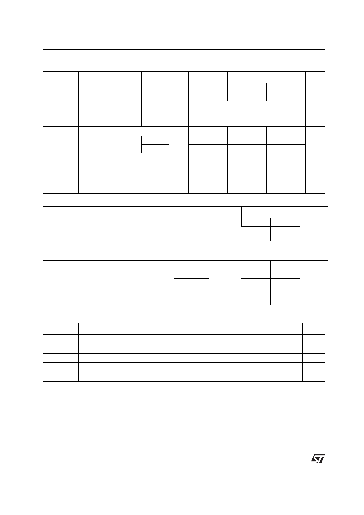
Symbol Value Unit
I
T(RMS)
V
DRM/VRRM
I
GT (Q1)
8A
600 and 800 V
5 to 50 mA
DESCRIPTION
Available either in through-hole or surface-mount
packages, the BTA/BT B08 and T8 triac series is
suitable for general purpose AC sw itching. They
can be used as an ON/OFF function in
applications such as static relays, heating
regulation, induction motor starting circuits... or for
phase control operation in light dimmers, motor
speed controllers,...
The snubberless versions (BTA/BTB...W and T8
series) are specially recommended for use on
inductive loads, than ks to their high com mutation
performances. By usin g an internal ceramic pa d,
the BTA series provides voltage insulated tab
(rated at 2500V RMS) complying with UL
standards (File ref.: E81734)
A2
A1
A2
G
DPAK
(T8-B)
A1
A2
G
A1
A2
G
TO-220AB Insulated
(BTA08)
G
IPAK
(T8-H)
A2
A1
A1
A2
A2
A1
A2
D2PAK
(T8-G)
G
TO-220AB
(BTB08)
A2
G
A2
ABSOLUTE MAXIMUM RATINGS
Symbol Parameter Value Unit
I
T(RMS)
I
TSM
²
I
dI/dt
I
GM
P
G(AV)
T
stg
T
RMS on-state current (full sine wave)
Non repetitive surge peak on-state
current (full cycle, Tj initial = 25°C)
tI
²
t Value for fusing
Critical rate of rise of on-state current
I
G
Peak gate current tp = 20 µs Tj = 125°C 4 A
Average gate power dissipation Tj = 125°C 1 W
Storage junction temperature range
Operating junction temp erature range
j
April 2002 - Ed: 5A
= 2 x IGT , tr ≤ 100 ns
DPAK / D
IPAK / TO-220AB
TO-220AB Ins. Tc = 100°C
F = 120 Hz Tj = 125°C 50 A/µs
²
PAK
Tc = 110°C
8A
F = 50 Hz t = 20 ms 80 A
F = 60 Hz t = 16.7 ms 84
tp = 10 ms 36
- 40 to + 150
- 40 to + 125
A
°C
²
s
1/10
BTA/BTB08 and T8 Series
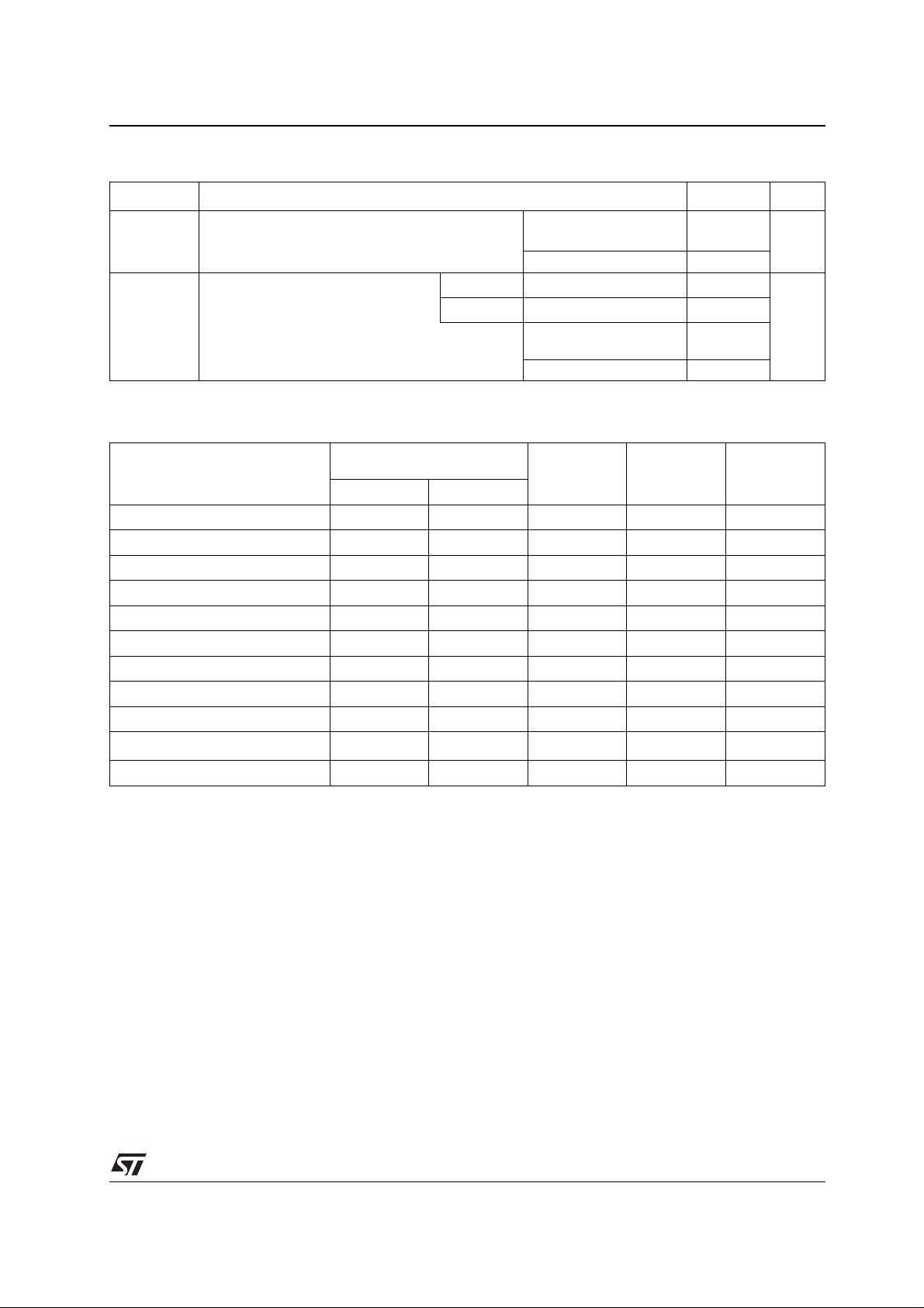
ELECTRICAL CHARACTERISTICS (Tj = 25°C, unless otherwise specified)
■ SNUBBERLESS™ and LOGIC LEVEL (3 Quadrants)
Symbol Test Conditions Quadrant T8 BTA/BTB08 Un it
T810 T835 TW SW CW BW
I
GT
V
V
(1)
GT
GD
= 12 V RL = 30 Ω
V
D
VD = V
RL = 3.3 kΩ
DRM
I - II - III MAX. 10 35 5 10 35 50
I - II - III MAX. 1.3 V
I - II - III MIN. 0.2
Tj = 125°C
I
(2)
H
I
L
= 100 mA
I
T
I
= 1.2 I
G
GT
MAX.153510153550mA
I - III MAX. 25 50 10 25 50 70 mA
II 30 60 15 30 60 80
dV/dt (2) V
= 67 %V
D
Tj = 125°C
(dI/dt)c (2) (dV/dt)c = 0.1 V/µs
gate open
DRM
Tj = 125°C MIN. 5.4 - 3.5 5.4 - - A/ms
MIN. 40 400 20 40 400 1000 V/µs
(dV/dt)c = 10 V/µs Tj = 125°C 2.8 - 1.5 2.8 - Without snubber
■ ST ANDARD (4 Quadrants)
Tj = 125°C - 4.5 - - 4.5 7
Symbol Test Conditions Quadra nt BTA/BTB08
CB
(1)
I
GT
V
GT
V
GD
I
(2)
H
I
L
= 12 V RL = 30 Ω
V
D
VD = V
= 500 mA
I
T
IG = 1.2 I
RL = 3.3 kΩ Tj = 125°C
DRM
GT
I - II - III
IV
MAX.
25
50
50
100
ALL MAX. 1.3 V
ALL MIN.
0.2 V
MAX. 25 50 mA
I - III - IV MAX. 40 50 mA
II 80 100
dV/dt (2) V
= 67 %V
D
gate open Tj = 125°C
DRM
MIN. 200 400 V/µs
(dV/dt)c (2) (dI/dt)c = 3.5 A/ms Tj = 125°C MIN. 5 10 V/µs
mA
Unit
mA
V
STATIC CHARACTERISTICS
Symbol Test Conditions Value Unit
V
(2) ITM = 11 A tp = 380 µs
TM
(2)
V
to
(2)
R
d
I
DRM
I
RRM
Note 1: minimum IGT is guaranted at 5% of IGT max.
Note 2: for both polarities of A2 referenced to A1
Threshold voltage Tj = 125°C MAX. 0.85 V
Dynamic resistance Tj = 125°C MAX. 50 mΩ
V
= V
DRM
RRM
2/10
Tj = 25°C MAX. 1.55 V
Tj = 25°C
Tj = 125°C 1 mA
MAX.
5µA
BTA/BTB08 and T8 Series
THERMAL RESISTANCES
Symbol Parameter Value Unit
R
th(j-c)
R
th(j-a)
S = Copper surface under tab
Junction to case (AC)
Junction to ambient
PRODUCT SELECTOR
S = 1 cm
S = 0.5 cm
DPAK / D
IPAK / TO-220AB
TO-220AB Insulated 2.5
²
²
TO-220AB Insulated
²
PAK
D²PAK
DPAK 70
TO-220AB
IPAK 100
1.6
45
60
°C/W
°C/W
Voltage (xxx)
Part Number
Sensitivity Type
Package
600 V 800 V
BTA/BTB08-xxxB X X 50 mA Standard TO-220AB
BTA/BTB108-xxxBW X X 50 mA Snubberless TO-220AB
BTA/BTB08-xxxC X X 25 mA Standard TO-220AB
BTA/BTB08-xxxCW X X 35 mA Snubberless TO-220AB
BTA/BTB08-xxxSW X X 10 mA Logic level TO-220AB
BTA/BTB08-xxxTW X X 5 mA Logic level TO-220AB
T810-xxxB X X 10 mA Logic level DPAK
T810-xxxH X X 10 mA Logic level IPAK
T835-xxxB X X 35mA Snubberless DPAK
T835-xxxG X X 35 mA Snubberless
²
D
PAK
T835-xxxH X X 35 mA Snubberless IPAK
BTB: non insulated TO-220AB package
3/10

BTA/BTB08 and T8 Series
ORDERING INFORMATION
BT A 08 - 600 BW (RG)
TRIAC
SERIES
INSULATION:
A: insulated
B: non insulated
CURRENT:8A
TRIAC
SERIES
CURRENT:8A
OTHER INFORMATION
Part Number Marking Weight
PACKING MODE
Bulk: Blank
RG:Tube
VOLTAGE:
600: 600V
800: 800V
SENSITIVITY &TYPE
B: 50mA STANDARD
BW: 50mA SNUBBERLESS
C: 25mA STANDARD
CW: 35mA SNUBBERLESS
SW: 10mA LOGIC LEVEL
TW: 5mA LOGIC LEVEL
T 8 10 - 600 B (-TR)
PACKAGE:
B: DPAK
2
VOLTAGE:
600: 600V
800: 800V
SENSITIVITY:
10: 10mA
35: 35mA
G: D PAK
H: IPAK
PACKING MODE:
Blank:Tube
-TR: DPAK / D PAK
Tape & Reel
Base
quantity
2
Packing
mode
BTA/BTB08-xxxyz BTA/BTB08xxxyz 2.3 g 250 Bulk
BTA/BTB08-xxxyzRG BTA/BTB08-xxxyz 2.3 g 50 Tube
T8yy-xxxB T8yyxxx 0.3 g 75 Tube
T8yy-xxxB-TR T8yyxxx 0.3 g 2500 Tape & reel
T8yy-xxxH T8yyxxx 0.4 g 75 Tube
T8yy-xxxG T8yyxxx 1.5 g 50 Tube
T8yy-xxxG-TR T8yyxxx 1.5 g 1000 Tape & reel
Note: xxx = voltage, yy = sensitivity, z = type
4/10

BTA/BTB08 and T8 Series
Fig. 1: Maximum power dissipation versus RMS
on-state current (full cycle).
P (W)
10
9
8
7
6
5
4
3
2
1
0
012345678
IT(RMS)(A)
Fig. 2-2: RMS on-state current versus ambient
temperature (printed circuit board FR4, copper
thickness: 35µm),full cycle.
IT(RMS) (A)
3.5
2
3.0
2.5
2.0
1.5
1.0
0.5
0.0
0 25 50 75 100 125
DPAK
(S=1cm )
DPAK
(S=0.5cm )
2
2
Tamb(°C)
Fig. 2-1: RMS on-state current versus case
temperature (full cycle).
IT(RMS) (A)
10
9
BTB/T8
8
7
6
BTA
5
4
3
2
1
0
0 25 50 75 100 125
Tc(°C)
Fig. 3: Relative variation of thermal impedance
versus pulse duration.
K=[Zth/Rth]
1E+0
1E-1
1E-2
1E-3
Zth(j-c)
DPAK/IPAK
Zth(j-a)
TO-220AB/D²PAK
Zth(j-a)
tp(s)
1E-3 1E-2 1E-1 1E+0 1E+1 1E+2 5E+2
Fig. 4: On-state characteristics (maximum
values).
ITM (A)
100
Tj max.
Vto = 0.85V
Rd = 50 m
Ω
10
1
0.5 1.0 1.5 2.0 2.5 3.0 3.5 4.0 4.5 5.0
Tj=Tj max
Tj=25°C
VTM(V)
Fig. 5: Surge peak on-state current versus
number of cycles.
ITSM (A)
90
80
70
60
50
40
30
Repetitive
Tc=100°C
Non repetitive
Tj initial=25°C
20
10
0
1 10 100 1000
Number of cycles
t=20ms
One cycle
5/10
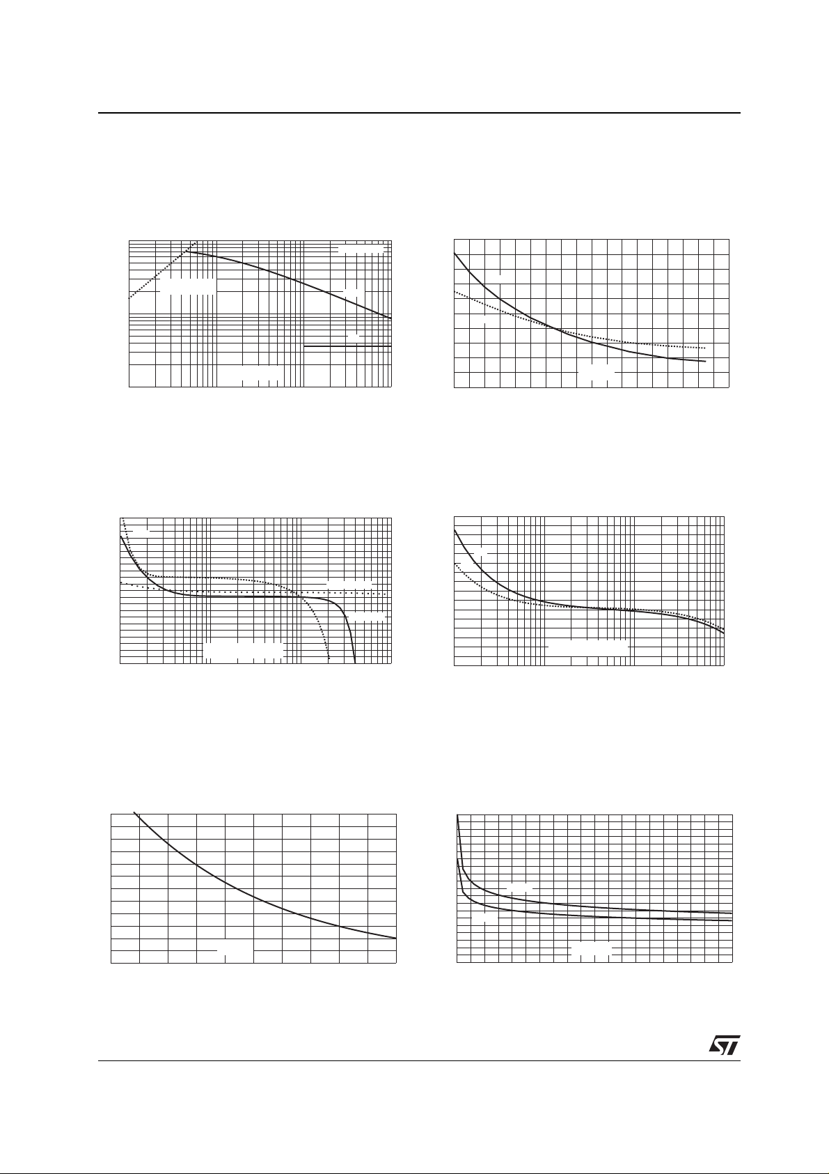
BTA/BTB08 and T8 Series
Fig. 6: Non-repetitive surge peak on-state
current for a sinusoidal pulse with width
tp < 10ms, and corresponding value of I²t.
ITSM (A), I²t (A²s)
1000
dI/dt limitation:
50A/µs
100
tp (ms)
10
0.01 0.10 1.00 10.00
Tj initial=25°C
ITSM
I²t
Fig. 8-1: Relative variation of critical rate of
decrease of main current versus (dV/dt)c (typical
values). Snubberless & Logic Lev el Types
(dI/dt)c [(dV/dt)c] / Specified (dI/dt)c
2.2
2.0
TW
1.8
1.6
1.4
1.2
1.0
0.8
0.6
0.4
0.2
0.0
0.1 1.0 10.0 100.0
(dV/dt)c (V/µs)
T835/CW/BW
T810/SW
Fig. 7: Relative variation of gate trigger current,
holding current and latching current versus
junction temperature (typical values).
IGT,IH,IL[Tj] / IGT,IH,IL [Tj=25°C]
2.5
2.0
IGT
1.5
1.0
IH & IL
0.5
Tj(°C)
0.0
-40 -20 0 20 40 60 80 100 120 140
Fig. 8-2: Relative variation of critical rate of
decrease of main current versus (dV/dt)c (typical
values). Standard Types
(dI/dt)c [(dV/dt)c] / Specified (dI/dt)c
2.0
1.8
1.6
1.4
1.2
1.0
0.8
0.6
0.4
C
B
(dV/dt)c (V/µs)
0.1 1.0 10.0 100.0
Fig. 9: Relative variation of critical rate of
decrease of main current versus junction
temperature.
(dI/dt)c [Tj] / (dI/dt)c [Tj specified]
6
5
4
3
2
1
0
0 25 50 75 100 125
6/10
Tj(°C)
Fig. 10: DPAK and D
2
PAK Thermal resistance
junction to ambien t versus copper surface under
tab (printed circuit board FR4, copper thickness:
35 µm).
Rth(j-a) (°C/W)
100
90
80
70
60
50
40
30
20
10
0
0 4 8 1216202428323640
DPAK
D²PAK
S(cm²)

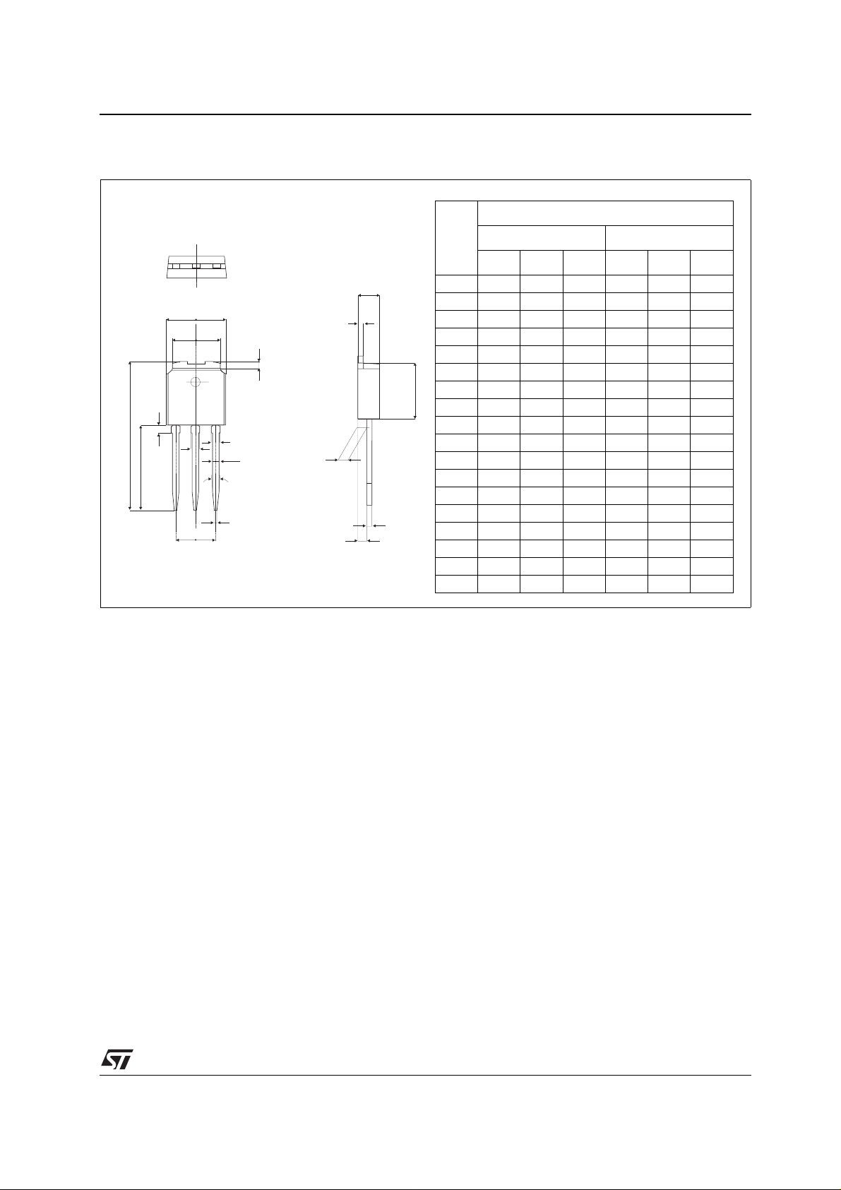
PACKAGE MECHANICAL DAT A
DPAK (Plastic)
BTA/BTB08 and T8 Series
DIMENSIONS
FOOTPRINT DIMENSIONS (in millimete r s )
DPAK (Plastic)
REF.
A 2.20 2.40 0.086 0.094
A1 0.90 1.10 0.035 0.043
A2 0.03 0.23 0.001 0.009
B 0.64 0.90 0.025 0.035
B2 5.20 5.40 0.204 0.212
C 0.45 0.60 0.017 0.023
C2 0.48 0.60 0.018 0.023
D 6.00 6.20 0.236 0.244
E 6.40 6.60 0.251 0.259
G 4.40 4.60 0.173 0.181
H 9.35 10.10 0.368 0.397
L2 0.80 typ. 0.031 typ.
L4 0.60 1.00 0.023 0.039
R 0.2 typ. 0.007 typ.
V2 0° 8° 0° 8°
Millimeters Inches
Min. Max Min. Max.
6.7
6.7
3
3
1.61.6
2.32.3
7/10

BTA/BTB08 and T8 Series
PACKAGE MECHANICAL DAT A
D²PAK (Plastic)
E
L2
L
L3
A1
B2
B
G
2.0 MIN.
FLAT ZONE
C2
DIMENSIONS
A
REF.
Millimeters Inches
Min. T yp. Max. Min. Typ. Max.
A 4.30 4.60 0.169 0.181
A1 2.49 2.69 0.098 0.106
D
A2 0.03 0.23 0.001 0.009
B 0.70 0.93 0.027 0.037
B2 1.25 1.40 0.048 0.055
C 0.45 0.60 0.017 0.024
C
R
C2 1.21 1.36 0.047 0.054
D 8.95 9.35 0.352 0.368
E 10.00 10.28 0.393 0.405
G 4.88 5.28 0.192 0.208
A2
L 15.00 15.85 0.590 0.624
L2 1.27 1.40 0.050 0.055
L3 1.40 1.75 0.055 0.069
V2
R 0.40 0.016
V2 0° 8° 0° 8°
FOOTPRINT DIMENSIONS (in millimete r s )
D²PAK (Plastic)
16.90
10.30
1.30
3.70
8.90
5.08
8/10
PACKAGE MECHANICAL DAT A
IPAK (Plastic)
BTA/BTB08 and T8 Series
DIMENSIONS
REF.
Millimeters Inches
Min. Typ. Max. Min. Typ. Max.
A
E
B2
L2
C2
A 2.2 2.4 0.086 0.094
A1 0.9 1.1 0.035 0.043
A3 0.7 1.3 0.027 0.051
B 0.64 0.9 0.025 0.035
B2 5.2 5.4 0.204 0.212
B3 0.85 0.033
D
B5 0.3 0.035
B6 0.95 0.037
C 0.45 0.6 0.017 0.023
H
L1
L
B6
B3
B
V1
A1
C2 0.48 0.6 0.019 0.023
D 6 6.2 0.236 0.244
E 6.4 6.6 0.252 0.260
G 4.4 4.6 0.173 0.181
B5
G
C
A3
H 15.9 16.3 0.626 0.641
L 9 9.4 0.354 0.370
L1 0.8 1.2 0.031 0.047
L2 0.8 1 0.031 0.039
V1 10° 10°
9/10

BTA/BTB08 and T8 Series
PACKAGE MECHANICAL DAT A
TO-220AB Ins.
B
C
b2
REF.
Millimeters Inches
DIMENSION S
Min. Typ. Max. Min. Typ. Max.
L
I
A
F
A 15.20 15.90 0.598 0.625
a1 3.75 0.147
a2 13.00 14.00 0.511 0.55 1
B 10.00 10.40 0.393 0.409
b1 0.61 0.88 0.02 4 0.034
l4
b2 1.23 1.32 0.04 8 0.051
C 4.40 4 .60 0.173 0.181
a1
l3
l2
a2
c2
c1 0.49 0 .70 0.019 0.027
c2 2.40 2 .72 0.094 0.107
e 2.40 2.70 0.09 4 0.106
F 6.20 6.60 0.244 0.259
I 3.75 3.85 0.147 0.151
I4 1 5.80 16.40 16.80 0.622 0.646 0.661
L 2.65 2.95 0.10 4 0.116
b1
e
M
c1
l2 1.14 1 .70 0.044 0.066
l3 1.14 1 .70 0.044 0.066
M 2.60 0.102
Information furnished is believed to be ac curate and reliable. However, STMicroelectronics assumes no responsibility for the c o nsequence s
of use of such information nor for any infringement of patents or other rights of third parties which may result from its use. No license is granted
by implic ation or ot herwise under any pa tent or paten t rights of S T M i croelectronics. Specification s mentioned i n this pub l i cation are sub j ect
to change without notice. This publication supersedes and replaces all information previously supplied. STMicroelectronics products are not
authoriz ed for use as critical comp onents in life support devi ces or syste m s wi t hout expre ss written appr oval of STMic roelectronics.
© The ST logo is a registe red trademark of STMicroelectron i cs
© 2002 STMi croelectr oni cs - Printed in It aly - All Rights Reserved
STMicroele ctronics GROUP OF COMPANIES
Australi a - Brazil - Canada - China - F i nl and - France - Germany
Hong Kong - India - Isr eal - Italy - Japan - M alaysia - Mal t a - Morocco - Singapore
Spain - Sweden - Switzerland - United Kingdom - Unit ed States.
http:// ww w.st.com
10/10
 Loading...