

Overview
The LC72323 is a single-chip microcontroller for use in
electronic tuning applications. It includes on chip both
LCD drivers and a PLL circuit that can operate at up to
150 MHz. It features a highly efficient instruction set, and
powerful hardware.
Functions
• Stack: Eight levels
• Fast programmable divider
• General-purpose counters: HCTR for frequency
measurement and LCTR for frequency or period
measurement
• LCD driver for displays with up to 56 segments
(1/2 duty, 1/2 bias)
• Program memory (ROM): 3 k words by 16 bits
• Data memory (RAM): 256 4-bit digits
• All instructions are single-word instructions
• Cycle time: 2.67 µs, 13.33 µs, or 40.00 µs (option)
• Unlock FF: 0.55 µs detection, 1.1 µs detection
• Timer FF: 1 ms, 5ms, 25ms, 125ms
• Input ports*: One dedicated key input port and one
high-breakdown voltage port
• Output ports*: Two dedicated key output ports, one
high-breakdown voltage open-drain port
Two CMOS output ports (of which one
can be switched to be used as LCD driver
outputs)
Seven CMOS output ports (mask option
switchable to use as LCD ports)
• I/O ports*: One switchable between input and output
in four-bit units and one switchable
between input and output in one-bit units
Note: * Each port consists of four bits.
• Program runaway can be detected and a special address
set (Programmable watchdog timer).
• Voltage detection type reset circuit
• One 6-bit A/D converter
• One external interrupt
• Hold mode for RAM backup
• Sense FF for hot/cold startup determination
• PLL: 4.5 to 5.5 V
• CPU: 3.5 to 5.5 V
• RAM: 1.3 to 5.5 V
• Package: QIP80E
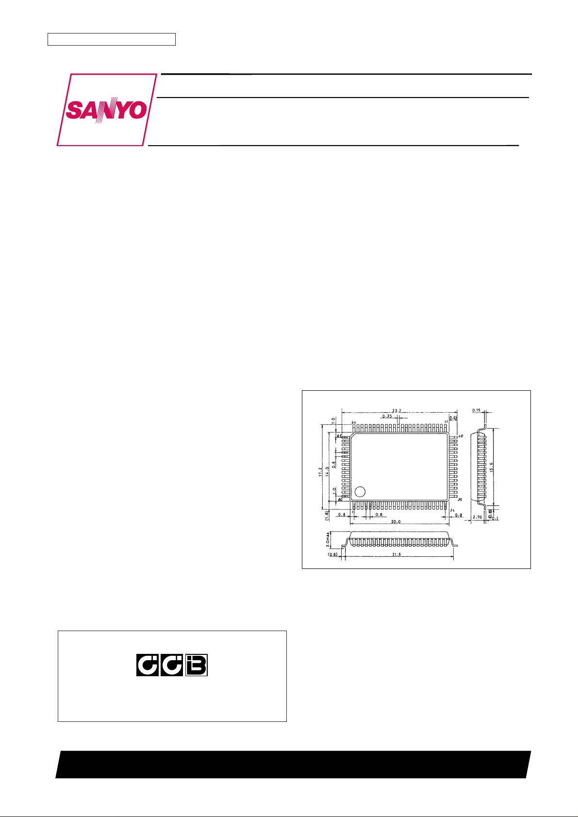
Package Dimensions
unit: mm
3174-QFP80E
CMOS LSI
32896HA (OT)/31595TH (OT) No. 4950-1/13
SANYO: QFP80E
[LC72323]
SANYO Electric Co.,Ltd. Semiconductor Bussiness Headquarters
TOKYO OFFICE Tokyo Bldg., 1-10, 1 Chome, Ueno, Taito-ku, TOKYO, 110 JAPAN
Single-Chip Microcontroller with PLL
and LCD Driver
LC72323
Ordering number : EN4950A
This LSI can easily use CCB that is SANYO’s original bus format.
• CCB is a trademark of SANYO ELECTRIC CO., LTD.
• CCB is SANYO’s original bus format and all the bus
addresses are controlled by SANYO.
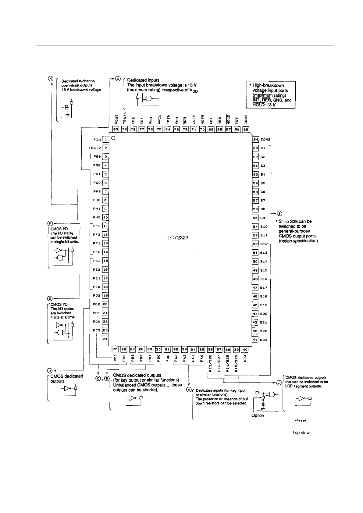
Pin Assignment
No. 4950-2/13
LC72323
No. 4950-3/13
LC72323
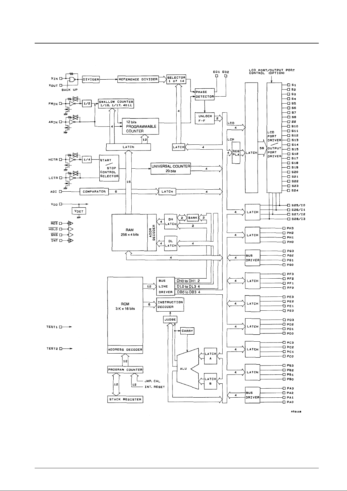
Block Diagram
No. 4950-4/13
LC72323
Specifications
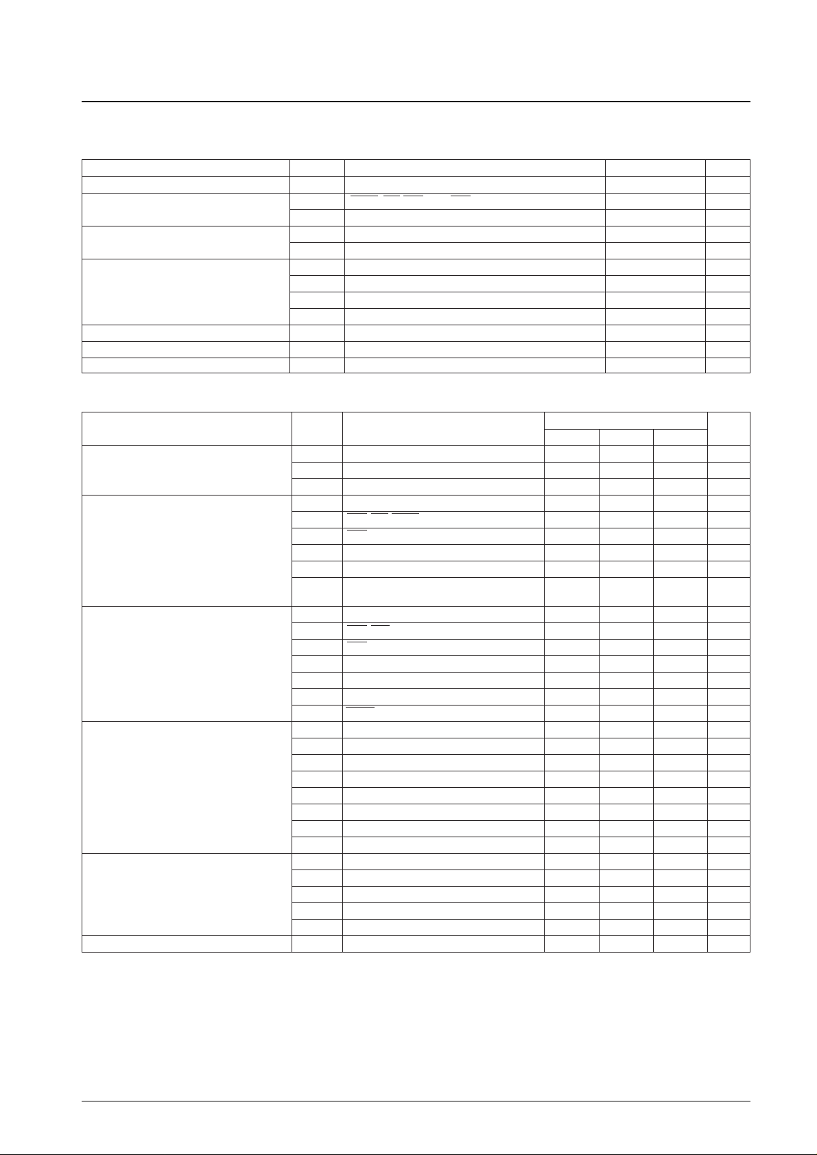
Absolute Maximum Ratings at Ta = 25°C, VSS= 0 V
Parameter Symbol Conditions Ratings Unit
Maximum supply voltage V
DD
max –0.3 to +6.5 V
Input voltage
V
IN
1 HOLD, INT, RES, ADI, SNS, and the G port –0.3 to +13 V
V
IN
2 Inputs other than VIN1 –0.3 to VDD+ 0.3 V
Output voltage
V
OUT
1 H port –0.3 to +15 V
V
OUT
2 Outputs other than V
OUT
1 –0.3 to VDD+ 0.3 V
I
OUT
1 All D and H port pins 0 to 5 mA
Output current
I
OUT
2 All E and F port pins 0 to 3 mA
I
OUT
3 All B and C port pins 0 to 1 mA
I
OUT
4 S1 to S28 and all I port pins 0 to 1 mA
Allowable power dissipation Pd max Ta = –40 to +85°C 300 mW
Operating temperature Topr –40 to +85 °C
Storage temperature Tstg –45 to +125 °C
Parameter Symbol Conditions
Ratings
Unit
min typ max
V
DD
1 CPU and PLL operating 4.5 5.5 V
Supply voltage V
DD
2 CPU operating 3.5 5.5 V
V
DD
3 Memory retention voltage 1.3 5.5 V
V
IH
1 G port 0.7 V
DD
8.0 V
V
IH
2 RES, INT, HOLD 0.8 V
DD
8.0 V
Input high level voltage
V
IH
3 SNS 2.5 8.0 V
V
IH
4 A port 0.6 V
DD
V
DD
V
V
IH
5 E and F ports 0.7 V
DD
V
DD
V
V
IH
6
LCTR (period measurement),
0.8 V
DD
V
DD
V
V
DD
1, PE1 and PE3
V
IL
1 G port 0 0.3 V
DD
V
V
IL
2 RES, INT, PE1, PE3 0 0.2 V
DD
V
V
IL
3 SNS 0 1.3 V
Input low level voltage V
IL
4 A port 0 0.2 V
DD
V
V
IL
5 PE0, PE2 and F ports 0 0.3 V
DD
V
V
IL
6 LCTR (period measurement), VDD1 0 0.2 V
DD
V
V
IL
7 HOLD 0 0.4 V
DD
V
f
IN
1 XIN 4.0 4.5 5.0 MHz
f
IN
2 FMIN, VIN2, VDD1 10 130 MHz
f
IN
3 FMIN, VIN3, VDD1 10 150 MHz
Input frequency
f
IN
4 AMIN (L), VIN4, VDD1 0.5 10 MHz
f
IN
5 AMIN (H), VIN5, VDD1 2.0 40 MHz
f
IN
6 HCTR, VIN6, VDD1 0.4 12 MHz
f
IN
7 LCTR (frequency), VIN7, VDD1 100 500 kHz
f
IN
8 LCTR (period), VIH6, VIL6, VDD1 1 20 ×10
3
Hz
V
IN
1 XIN 0.50 1.5 Vrms
V
IN
2 FMIN 0.10 1.5 Vrms
Input amplitude V
IN
3 FMIN 0.15 1.5 Vrms
V
IN
4, 5 AMIN 0.10 1.5 Vrms
V
IN
6, 7 LCTR, HCTR 0.10 1.5 Vrms
Input voltage range V
IN
8 ADI 0 V
DD
V
Allowable Operating Ranges at Ta = –40 to +85°C, VDD= 3.5 to 5.5 V
 Loading...