


Overview
The LC65P29 is a one-time programmable (on-chip
PROM) version of Sanyo's LC6529N/F/L 4-bit single-chip
CMOS microcontroller. It provides identical functionality
to, and pin compatibility with, the mask ROM versions of
the LC6529N/F/L, and provides a 1-KB internal PROM.
The LC65P29 is provided in DIP24S and MFP30S plastic
packages and the program can be written by the customer,
thus makes this IC appropriate for the limited-run products
and the startup of initial production of new products.
Furthermore, it can provide reduced changeover periods
when end product specifications change.
Additionally, the LC65P29 can function as a one-time
programmable PROM version of the Sanyo LC6527N/F/L
and LC6528N/F/L by using the 29T27 adapter socket.
Features
• Mask option settings can be switched by setting PROM
data.
All options, except for the port output circuit type can be
set with PROM data.
• 1-KB PROM
• PROM data security function
• Pin compatible with the mask ROM version
• Instruction cycle time: 0.92 µs to 20 µs
• Packages: DIP24S and MFP30S
Package Dimensions
unit: mm
3067-DIP24S(300mil)
unit: mm
3216-MFP30S(375mil)
Note: The package dimension figures are provide for reference purposes
without dimensional tolerances. Contact your Sanyo representative
for the official package dimension figures.
CMOS IC
61298RM (OT) No. 5894-1/14
SANYO: DIP24S(300mil)
[LC65P29]
SANYO: MFP30S(375mil)
[LC65P29]
SANYO Electric Co.,Ltd. Semiconductor Bussiness Headquarters
TOKYO OFFICE Tokyo Bldg., 1-10, 1 Chome, Ueno, Taito-ku, TOKYO, 110-8534 JAPAN
One-Time Programmable 4-Bit Single-Chip
Microcontroller
LC65P29
Ordering number : EN5894
No. 5894-2/14
LC65P29
Product Series Structure
Notes on Sanyo ROM Writing Services
Sanyo provides a for-fee ROM writing service that consists of writing the one-time programmable ROM , printing,
screening, and readout verification. Contact your Sanyo representative for details.
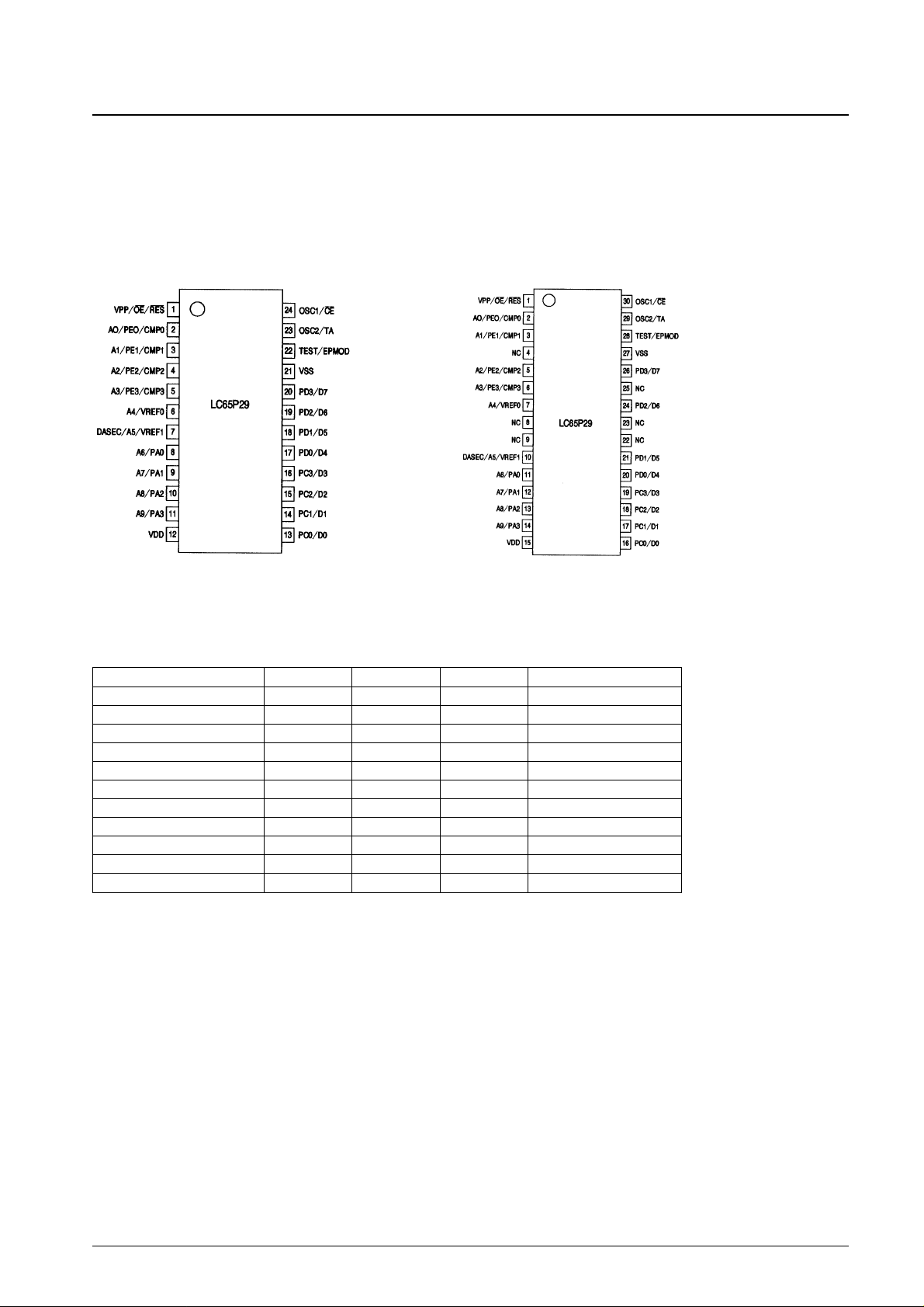
Pin Assignments
DIP24S
Type number. Number of pins ROM capacity RAM capacity Package
LC6527N/F/L, LC6528N/F/L 18 1K, 0.5K 64W, 32W DIP18, MFP18
LC6529N/F/L 24/30 1K 64W DIP24S, SSOP24, MFP30S
LC65E29 24/30 1K 64W DIC24S, MFC30S
LC65P29 24/30 1K 64W DIP24S, MFP30S
LC6543N/F/L, LC6546N/F/L 30 2K, 1K 128W, 64W DIP30S, MFP30S
LC65E43 30 2K 128W, 64W DIC30S, MFC30S
LC65P43 30 2K 128W, 64W DIP30S, MFP30S
LC651104N/F/L, LC651102N/F/L 30 4K, 2K 256W DIP30S, MFP30S
LC651204N/F/L, LC651202N/F/L 30 4K, 2K 256W DIP30S, MFP30S
LC65E1104 30 4K 256W DIC30S, MFC30S
LC65P1104 30 4K 256W DIP30S, MFP30S
MFP30S
Top view Top view
Usage Notes
The LC65P29 is designed for program development and evaluation for systems that use the LC6529N/F/L. The following
points require attention when using this product.
• Mounting notes
Due to the nature of the device, one-time programmable microcontrollers cannot be fully tested prior to shipment. This
means that users must perform the screening process described on page 14.
• ROM ordering procedure when using the Sanyo for-fee ROM writing service
The customer must abide by the following when using the Sanyo for-fee ROM writing service:
— When ordering both one-time programmable and mask versions at the same time
The customer must provide an EPROM for the mask version, the mask version order forms, and the one-time
programmable version order forms.
— When order only the one-time programmable version
The customer must provide an EPROM for the one-time programmable version and the one-time programmable
version order forms. The end area in the EPROM (locations 400 to 404H) is the option specification area and the
customer must program the option specification data in that area. The customer must use the cross assembler
specified by Sanyo.
• Differences between the LC65P29 and the LC6529N/F/L
No. 5894-3/14
LC65P29
Parameter LC65P29 LC6529N LC6529F LC6529L
OptionCharacteristicOther items
Ports C and D output option
during reset
High or low can be
specified (option code)
High or low can be specified (mask option)
Port output type during reset
Open-drain output only
(ports A, C, and D)
Open-drain or pull-up register can be specified (mask option)
Oscillator circuit option
CF/RC or EXT can be
specified (option code)
CF/RC or EXT can be
specified (mask option)
CF or EXT can be
specified (mask option)
CF/RC or EXT can be
specified (mask option)
Divider circuit option
1/1, 1/3, or 1/4 can be
specified (option code)
1/1,1/3 or 1/4 can be
specified (mask option)
Only 1/1 is possible
(mask option)
1/1,1/3 or 1/4 can be
specified (mask option)
Comparator input and port E input
option
Comparator or port E can
be specified (option code)
Comparator or port E can be specified (mask option)
Comparator function option
Feedback resistor present
or absent can be specified
(option code)
Feedback resistor present or absent can be specified (mask option)
Minimum cycle time
0.92 µs (VDD≥ 3.0 V) 2.77 µs (VDD≥ 3.0 V) 0.92 µs (VDD≥ 3.0 V) 3.84 µs (VDD≥ 2.2 V)
Operating temperature –30 to +70°C –40 to +85°C
Supply voltage 3.0 to 6.0 V 3.0 to 6.0 V 3.0 to 6.0 V 2.2 to 6.0 V
Current drain 5.0 mA typ. 2.0 mA typ. 2.5 mA typ. 2.0 mA typ.
Reset port input low-level current –50 µA typ. –10 µA typ.
Package DIP24S, MFP30S DIP24S, SSOP24, MFP30S
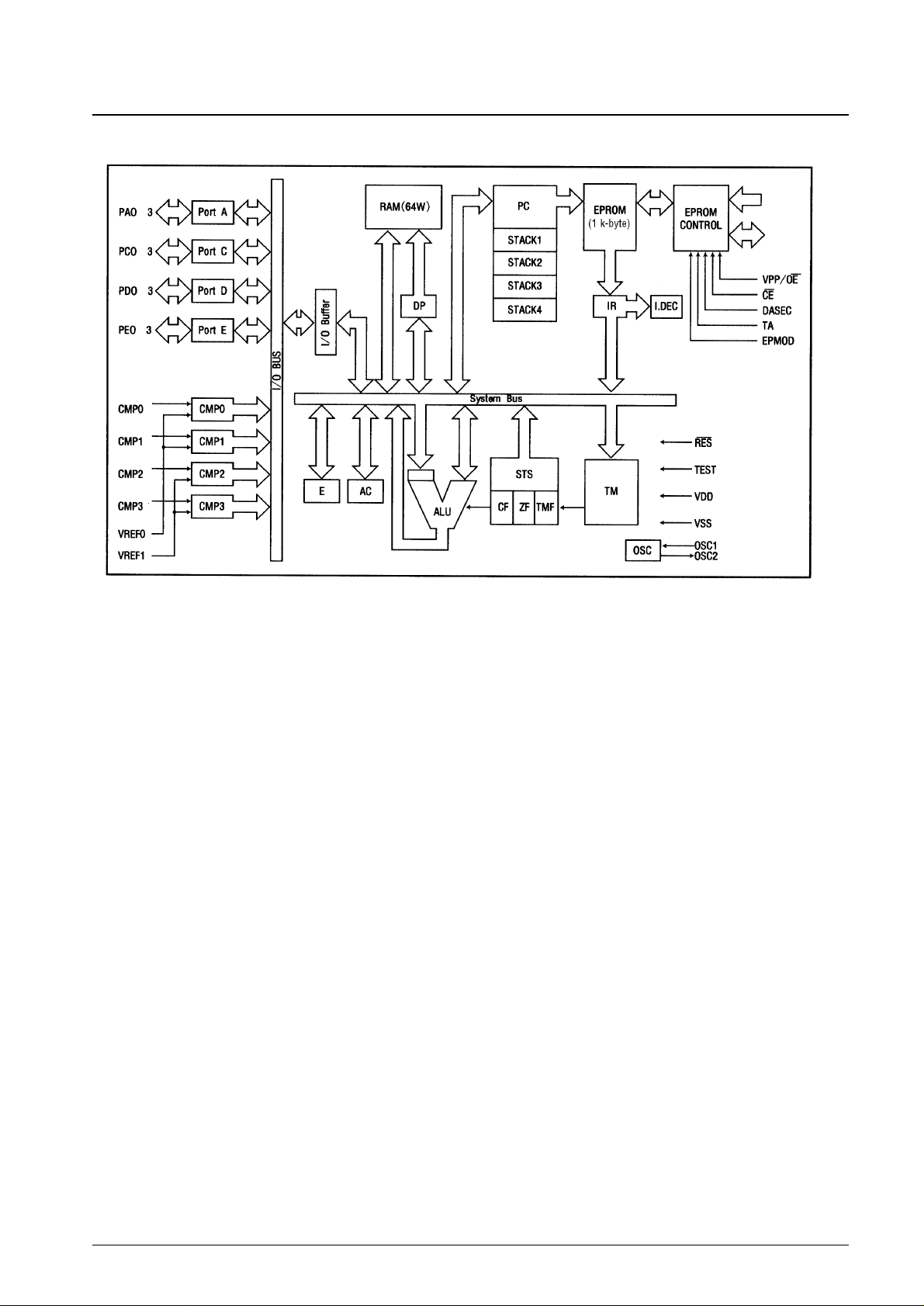
System Block Diagram
No. 5894-4/14
LC65P29
RAM:Data memory
ALU: Arithmetic and logic unit
DP: Data pointer
E: E register
AC: Accumulator
OSC: Oscillator circuit
TM: Timer
STS: Status register
EPROM: Program memory
PC: Program counter
I.R: Instruction register
I.DEC: Instruction decoder
CF: Carry flag
ZF: Zero flag
TMF: Timer overflow flag
to
toto
to
to
A0 to A9
D0 to D7

No. 5894-5/14
LC65P29
Pin Descriptions
Pin name
Number
I/O Function Option State during reset
Function in
of pins PROM mode
Power supply. Must be connected to +5 V
during normal operation.
Power supply. Must be connected to 0 V
during normal operation.
—
—
V
DD
V
SS
1
1
—
—
System clock oscillator connections. Leave
OSC2 open and input the external clock to
OSC1 if an external clock is used.
1.Two-pin RC oscillator
(Single-pin external
clock input)
2.Two-pin ceramic
oscillator
3.Divisor option: 1/1, 1/3,
or 1/4
EPROM contorol
signal inputs
CE
TA
OSC1/CE
OSC2/TA
1
I
O
• I/O ports A0 to A3
Input in 4-bit units (IP instruction)
Output in 4-bit units (OP instruction)
Data testing in 1-bit units (BP and BNP
instructions)
Data set and clear operations in 1-bit units
(SPB and RPB instructions)
• PA3 is used for standby mode control.
• Applications must assure that chattering
(key bounce) noise is not input during a
HALT instruction execution cycle.
Open-drain output
• High-level output (The
n-channel output
transistor turned off.)
• Address inputs
A6 to A9
PA0/A6
PA1/A7
PA2/A8
PA3/A9
4 I/O
• I/O ports C0 to C3
The pin functions are identical to those of
pins A0 to A3.
However, there is no standby mode
control function.
• The output during a reset can be specified
to be either high or low as an option.
1. Open-drain output
2. High-level output
during reset
3. Low-level output
during reset
• Selection of items 2 or
3 is in 4-bit units.
• High-level output
• Low-level output
(Depending on an
option selection.)
• Data I/O
D0 to D3
PC0/D0
PC1/D1
PC2/D2
PC3/D3
4 I/O
• I/O ports D0 to D3
The pin functions are identical to those of
pins PC0 to PC3.
The same as for pins
PC0 to PC3
The same as pins PC0 to
PC3
• Data I/O
D4 to D7
PD0/D4
PD1/D5
PD2/D6
PD3/D7
4 I/O
• When comparator input is selected:
CMP0 and CMP1 use V
REF
0 as the
reference voltage,
CMP2 and CMP3 use V
REF
1 as the
reference voltage,
• Comparator inputs CMP0 to CMP3
Data input in 4-bit units (IP instruction)
• Data testing in 1-bit units (BP and BNP
instructions)
1. Comparator input
2. Port E input
3. No feedback resistor
4. Feedback resistor
present
• Selection of items 1 or
2 is in 4-bit units.
• Items 3 and 4 are only
specified when item 1
is selected.
• Address inputs
A0 to A3
PE0/CMP0/A0
PE1/CMP1/A1
PE2/CMP2/A2
PE3/CMP3/A3
4 I
• Comparator reference voltage inputs
V
REF
0 and V
REF
1
V
REF
0 is the reference voltage input for
CMP0 and CMP1.
V
REF
1 is the reference voltage input for
CMP2 and CMP3.
• When PE0/CMP0 to PE3/CMP3 are
selected to function as port E inputs,
these pins are connected to V
SS
.
• Address inputs
A4 and A5
• EPROM control
signal input
DASEC
V
REF
0/A4
V
REF
1/A5/
DASEC
2 I
• System reset input
• Connect an external capacitor to effect the
power-on reset.
• Input a low level for at least 4 clock cycles
to effect a reset restart.
• EPROM control
signal input
V
PP
/ OE
RES/V
PP
/OE
1 I
• IC test pin
This pin must be connected to V
SS
during
normal operation.
• EPROM control
signal input
EPMOD
TEST/EPMOD 1 I
• When input is selected for port E
• Input ports E0 to E3
Input in 4-bit units (IP instruction)
• Data testing in 1-bit units (BP and BNP
instructions)
4 I
 Loading...