

SANYO LC6529F, LC6529N, LC6529L Datasheet

CMOS LSI
Ordering number : EN*5117
92995HA (OT) No. 5117-1/39
Preliminary
SANYO Electric Co.,Ltd. Semiconductor Bussiness Headquarters
TOKYO OFFICE Tokyo Bldg., 1-10, 1 Chome, Ueno, Taito-ku, TOKYO, 110-8534 JAPAN
4-Bit Microcomputer
for Small-Scale Control Applications
LC6529N, LC6529F, LC6529L
Overview
The LC6529N/F/L provides the basic architecture and
instruction set of the Sanyo LC6500 Series of 4-bit singlechip microcomputers in a version specially for small-scale
control applications involving circuits built with standard
logic elements, applications using simple, comparatorbased voltage or phase detectors, or other applications
controlling a limited number of controls. The LC6529F is
a replacement for the former LC6529H. (Certain functions
differ, however.) The N (medium-speed) and L (powersaving) versions are new additions to the lineup.
Features
• Power-saving CMOS design (Standby mode accessed
with HALT instruction included.)
• Memory: 1 kilobyte of 8-bit ROM and 64 words of 4-bit
RAM
• Instruction set: 51-member subset of LC6500 standard
complement of 80 instructions
• (L version) Wide range of operating voltages:
2.2 to 6.0 V
• (F version) 0.92 µs/3.0 V instruction cycle time
• Flexible I/O ports
Four ports with up to 16 lines
— Bidirectional I/O ports: 12
Dedicated input ports: 4 (These double as
comparator inputs.)
— I/O voltage limit: max. +15 V (open-drain
configuration)
— Output current: max. 20 mA sink current (capable of
directly driving an LED)
Choice of options to match system specifications
— Choice of open-drain or pull-up resistor output
configurations at the bit level for all ports
— Choice of reset output levels for Ports C and D in
groups of 4 bits each
Port E configurable as four comparator inputs
• Stack: Four levels
• Timers: 4-bit prescaler plus 8-bit programmable counter
• Comparators: 4 channels (2 reference levels)
Separator reference level for each channel pair
— Feedback resistor option for choice of input with or
without hysteresis
• Choice of clock oscillator options to match system
specifications
— Oscillator circuit options: 2-pin RC oscillator circuit
(N and L versions) or 2-pin ceramic oscillator circuit
(N, F, and L versions)
— Frequency divider options: Built-in 1/3 and 1/4
frequency dividers that eliminate the need for
external frequency dividers
Summary of Functions
Note: The oscillator constants will be announced once the recommended circuit design has been decided.
No. 5117-2/39
LC6529N, LC6529F, LC6529L
Item LC6529N LC6529F LC6529L
[Memory]
ROM 1024
× 8 bits 1024 × 8 bits 1024 × 8 bits
RAM 64 × 4 bits 64 × 4 bits 64 × 4 bits
Instruction set 51 51 51
[On-board functions]
Timers
4-bit prescaler plus 8-bit 4-bit prescaler plus 8-bit 4-bit prescaler plus 8-bit
programmable counter programmable counter programmable counter
Stack levels 4 4 4
Standby mode
HALT instruction places chip HALT instruction places chip HALT instruction places chip
on standby. on standby. on standby.
Comparators 4 channels (2 reference levels) 4 channels (2 reference levels) 4 channels (2 reference levels)
[I/O ports]
Number of ports 12 bidirectional I/O pins, 4 input pins 12 bidirectional I/O pins, 4 input pins 12 bidirectional I/O pins, 4 input pins
I/O voltage limit max. 15 V (ports A, C, and D) max. 15 V (ports A, C, and D) max. 15 V (ports A, C, and D)
Output current 10 mA typ. 20 mA max. 10 mA typ. 20 mA max. 10 mA typ. 20 mA max.
I/O circuit configuration Choice of open-drain output or pull-up resistors at the bit level for ports A, C, and D
Reset output level Choice of high or low in groups of 4 bits each (ports C and D)
Port function Port E configurable as four comparator inputs
[Characteristics]
Minimum cycle time 2.77 µs (V
DD
≥ 3.0 V) 0.92 µs (VDD≥ 3.0 V) 3.84 µs (VDD≥ 2.2 V)
Operating temperature –40 to +85°C –40 to +85°C –40 to +85°C
Power supply voltage 3.0 to 6.0 V 3.0 to 6.0 V 2.2 to 6.0 V
Current drain 1.1 mA typ. 1.6 mA typ. 1.0 mA typ.
[Clock]
RC (850 kHz, 400 kHz typ.) RC (400 kHz typ.)
Oscillator Ceramic oscillator (400 kHz, 800 kHz, Ceramic oscillator (2 MHz, 4 MHz) Ceramic oscillator (400 kHz, 800 kHz,
2 MHz, 4 MHz) 2 MHz, 4 MHz)
Frequency divider options 1/1, 1/3, 1/4 1/1 1/1, 1/3, 1/4
[Miscellaneous]
Package DIP24S, SSOP24, MFP30S DIP24S, SSOP24, MFP30S DIP24S, SSOP24, MFP30S
OTP Included Included Included
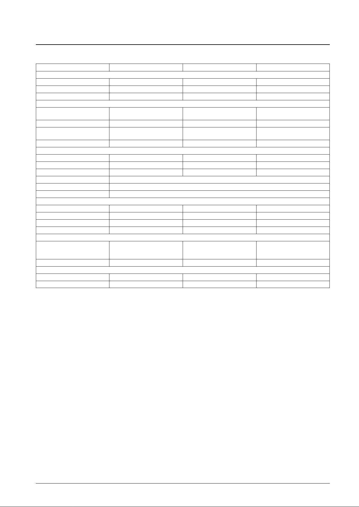
Pin Assignments
MFP30S
DIP24S/SSOP24
Note: Do not use dip-soldering when mounting the SSOP package on the
circuit board.
Package Dimensions
unit: mm
3073A-MFP30S
No. 5117-3/39
LC6529N, LC6529F, LC6529L
SANYO: MFP30S
[LC6529N, 6529F, 6529L]
unit: mm
3067-DIP24S
SANYO: DIP24S
[LC6529N, 6529F, 6529L]
unit: mm
3175A-SSOP24
SANYO: SSOP24
[LC6529N, 6529F, 6529L]
Note: The above diagrams give only the nominal dimensions. Contact Sanyo for drawings complete with tolerances.
Pin Names
OSC1, OSC2: Pins for RC or ceramic oscillator circuit
TEST: Test pin
RES: Reset pin
PA0 to PA3: Bidirectional I/O port A, bits 0 to 3
PC0 to PC3: Bidirectional I/O port C, bits 0 to 3
PD0 to PD3: Bidirectional I/O port D, bits 0 to 3
PE0 to PE3: Unidirectional input port E, bits 0 to 3
CMP0 to CMP3: Comparator input port, bits 0 to 3
VREF0, VREF1: Reference inputs
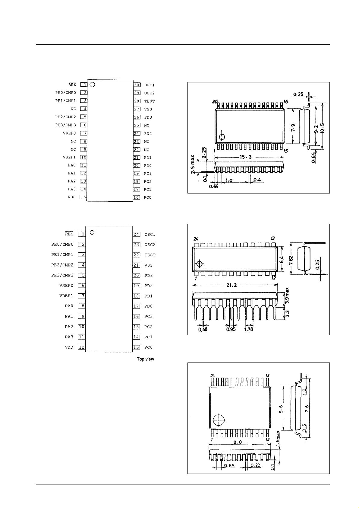
System Block Diagram
RAM: Data memory ROM: Program memory
AC: Accumulator PC: Program Counter
ALU: Arithmetic and Logic Unit IR: Instruction Register
DP: Data pointer I.DEC: Instruction Decoder
E: E register CF: Carry Flag
OSC: Oscillator circuit ZF: Zero Flag
TM: Timer TMF: Timer overflow Flag
STS: Status register
No. 5117-4/39
LC6529N, LC6529F, LC6529L
Pin Functions
No. 5117-5/39
LC6529N, LC6529F, LC6529L
Pin No. Symbol I/O Function Output driver type Options State after reset
V
DD
V
SS
OSC1
OSC2
PA0
PA1
PA2
PA3
PC0
PC1
PC2
PC3
PD0
PD1
PD2
PD3
PE0/CMP0
PE1/CMP1
PE2/CMP2
PE3/CMP3
V
REF
0
V
REF
1
RES
TEST
—
—
I
O
I/O
I/O
I/O
I
I
I
I
I
Power supply. Normally +5 V.
Power supply. 0 V.
Pins for attaching external system
clock oscillator circuit (RC or ceramic)
• Bidirectional I/O port A0 to A3: 4-bit
input (IP instruction), 4-bit output (OP
instruction), 1-bit conditionals (BP
and BNP instructions), 1-bit set and
reset (SPB and RPB instructions)
• PA3 also doubles as standby
operation control.
• Block chattering from entering PA3
during the HALT instruction
execution cycle.
• Bidirectional I/O port C0 to C3.
Functions the same as PA0 to PA3
except that there is no the standby
operation control.
• Option controls whether output is
high or low after reset.
Bidirectional I/O port D0 to D3.
Functions and options the same as
PC0 to PC3.
• When configured for comparator
input: CMP0 and CMP1 use
reference voltage V
REF
0; CMP2 and
CMP3 use reference voltage V
REF
1.
• 4-bit (CMP0 to 3) input (IP
instruction)
• 1-bit conditionals (BP and BNP
instructions)
• When configured for port E input:
• 4-bit (E0-3) input (IP instruction)
• 1-bit conditionals (BP and BNP
instructions)
• Comparator reference level inputs:
CMP0 and CMP1 use reference
voltage V
REF
0; CMP2 and CMP3
use reference voltage V
REF
1.
• Connect to V
SS
when PE0/CMP0 to
PE3/CMP3 configured as port E.
• System reset input
• Connect external capacitor for power
up reset.
• Low level input for a minimum of four
clock cycles triggers a reset.
Chip test pin. Normally connect to V
SS
.
• N channel: sink
current type
• I/O voltage limit for
open-drain
configuration: max.
+15 V
• P channel: highimpedance pull-up
type
• N channel: sink
current type
• I/O voltage limit for
open-drain
configuration: max.
+15 V
• P channel: lowimpedance pull-up
type
• N channel: sink
current type
• I/O voltage limit for
open-drain
configuration: max.
+15 V
• P channel: highimpedance pull-up
type
1
1
1
1
4
4
4
4
4
2
1
1
—
—
High output (output
N channel transistor
off)
High or low (option)
High or low (option)
—
—
1. 2-pin RC oscillator circuit
(1-pin external clock)
2. 2-pin ceramic oscillator circuit
3. Frequency divider options:
1/1, 1/3, 1/4
1. Open-drain output
2. Pull-up resistor
• Choice of configuration 1. or 2. at
bit level
1. Open-drain output
2. Pull-up resistor
3. High output after reset
4. Low output after reset
• Choice of configuration 1. or 2. at
bit level
• Choice of configuration 3. or 4. at
port (4-bit) level
1. Open-drain output
2. Pull-up resistor
3. High output after reset
4. Low output after reset
• Choice of configuration 1. or 2. at
bit level
• Choice of configuration 3. or 4. at
port (4-bit) level
1. Comparator input
2. Port E input
3. Without feedback resistor
4. With feedback resistor
• Choice of configuration 1. or 2. at
port (4-bit) level
• Options 3. and 4. only available
with 1.
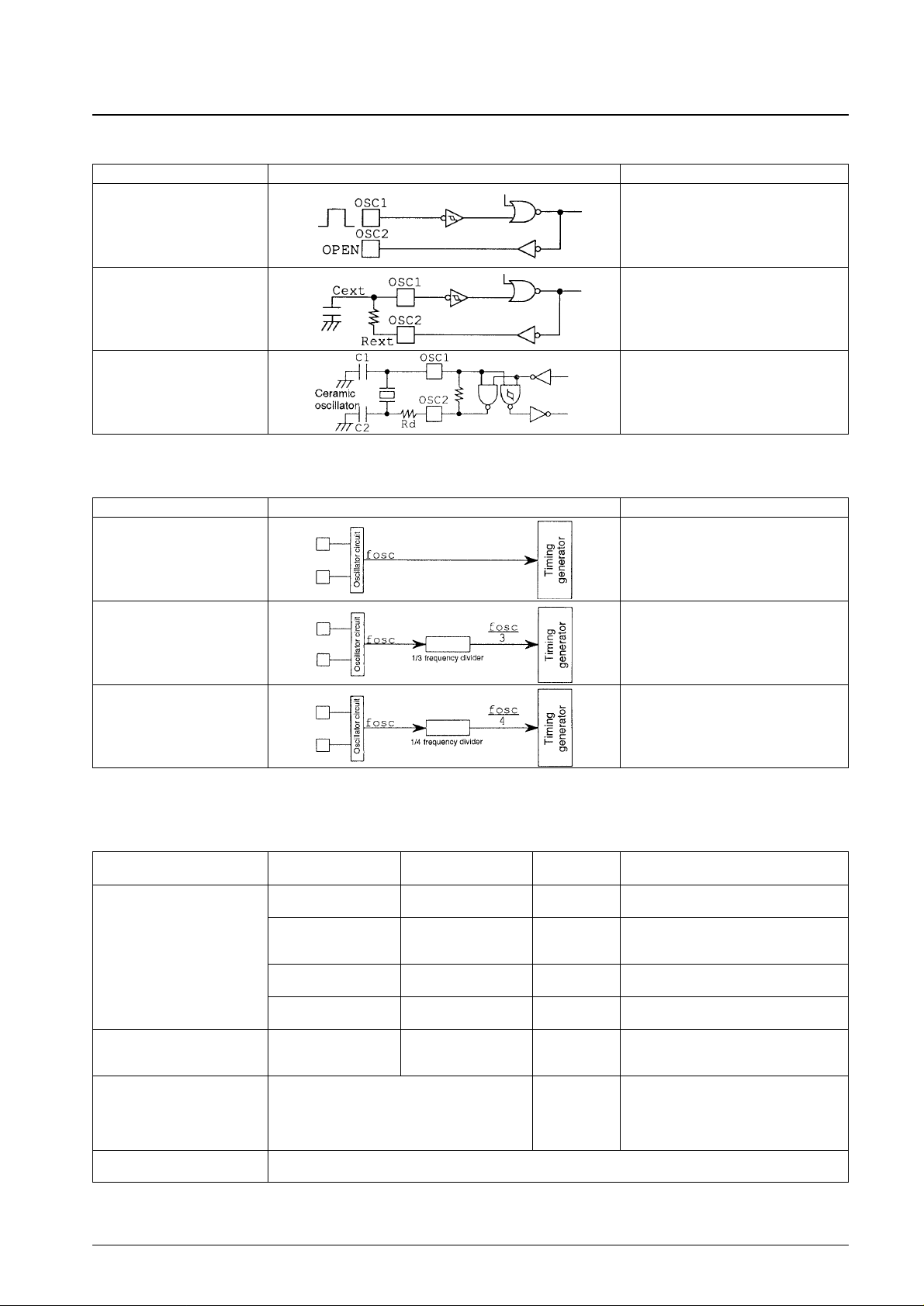
Oscillator Circuit Options
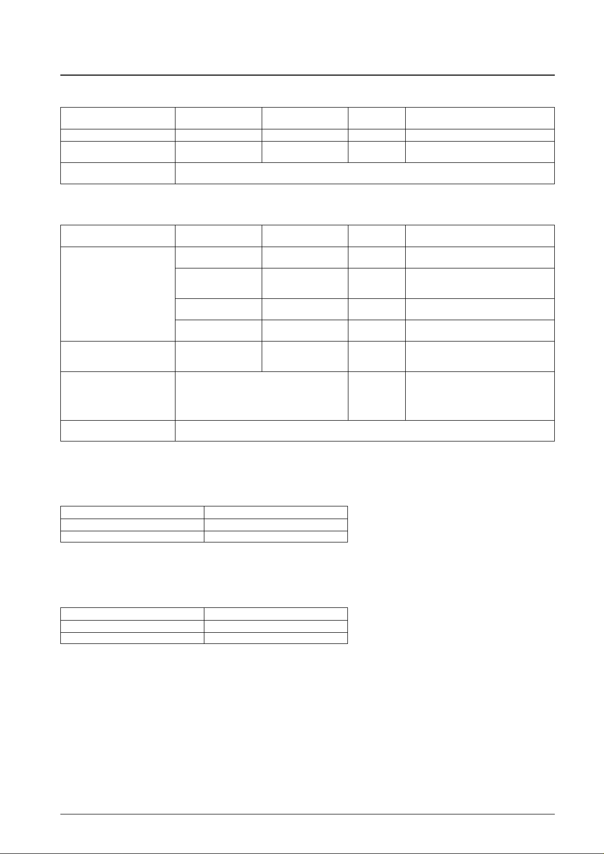
Frequency Divider Options
Frequency Divider Options
LC6529N
No. 5117-6/39
LC6529N, LC6529F, LC6529L
Name Circuit diagram Conditions, etc.
External clock
2-pin RC oscillator circuit
2-pin ceramic oscillator circuit
Leave OSC2 open.
Name Circuit diagram Conditions, etc.
No frequency divider (1/1)
1/3 frequency divider
1/4 frequency divider
Available with all three oscillator circuit options
(N, F, and L versions)
Available only with external clock and ceramic
oscillator circuit options (N and L versions)
Available only with external clock and ceramic
oscillator circuit options (N and L versions)
Oscillator circuit Frequency
Frequency divider options
VDDrange Note
(cycle time)
400 kHz 1/1 (10 µs) 3 to 6 V
1/3 and 1/4 frequency divider options
not available
1/1 (5 µs) 3 to 6 V
800 kHz 1/3 (15 µs) 3 to 6 V
Ceramic oscillator
1/4 (20 µs) 3 to 6 V
2 MHz
1/3 (6 µs) 3 to 6 V
1/1 frequency divider option not available
1/4 (8 µs) 3 to 6 V
4 MHz
1/3 (3 µs) 3 to 6 V
1/1 frequency divider option not available
1/4 (4 µs) 3 to 6 V
External clock based on RC
200 k to 1444 kHz 1/1 (20 to 2.77 µs) 3 to 6 V
oscillator circuit
600 k to 4330 kHz 1/3 (20 to 2.77 µs) 3 to 6 V
800 k to 4330 kHz 1/4 (20 to 3.70 µs) 3 to 6 V
Use 1/1 frequency divider and recommended
constants or, if this is not possible, one of the
RC oscillator circuit frequency, frequency divider option, and V
DD
range 3 to 6 V
combinations listed for external clocks based on
an RC oscillator circuit.
External clock based on ceramic
This configuration not allowed. Use an external clock based on an RC oscillator circuit instead.
oscillator circuit
LC6529F
LC6529L
Reset Level Options for Ports C and D
The following two options are available for controlling the output levels of ports C and D in groups of four bits each.
Comparator vs. Port E Configuration Option
The four pins PE0/CMP0 to PE3/CMP3 may be configured for comparator input or as port E.
No. 5117-7/39
LC6529N, LC6529F, LC6529L
Oscillator circuit Frequency
Frequency divider options
VDDrange Note
(cycle time)
Ceramic oscillator 4 MHz 1/1 (1 µs) 3 to 6 V
External clock based on RC
200 k to 4330 kHz 1/1 (20 to 0.92 µs) 3 to 6 V
oscillator circuit
External clock based on ceramic
This configuration not allowed. Use an external clock based on an RC oscillator circuit instead.
oscillator circuit
Oscillator circuit Frequency
Frequency divider options
VDDrange Note
(cycle time)
400 kHz 1/1 (10 µs) 2.2 to 6 V
1/3 and 1/4 frequency divider options
not available
1/1 (5 µs) 2.2 to 6 V
800 kHz 1/3 (15 µs) 2.2 to 6 V
Ceramic oscillator
1/4 (20 µs) 2.2 to 6 V
2 MHz
1/3 (6 µs) 2.2 to 6 V
1/1 frequency divider option not available
1/4 (8 µs) 2.2 to 6 V
4 MHz 1/4 (4 µs) 2.2 to 6 V
1/1 and 1/3 frequency divider options not
available
External clock based on RC
200 k to 1040 kHz 1/1 (20 to 3.84 µs) 2.2 to 6 V
oscillator circuit
600 k to 3120 kHz 1/3 (20 to 3.84 µs) 2.2 to 6 V
800 k to 4160 kHz 1/4 (20 to 3.84 µs) 2.2 to 6 V
Use 1/1 frequency divider and recommended
constants or, if this is not possible, one of the
RC oscillator circuit frequency, frequency divider option, and V
DD
range 2.2 to 6 V
combinations listed for external clocks based on
an RC oscillator circuit.
External clock based on ceramic
This configuration not allowed. Use an external clock based on an RC oscillator circuit instead.
oscillator circuit
Option Conditions, etc.
High level output after reset Selection affects all bits of port
Low level output after reset Selection affects all bits of port
Option Conditions, etc.
Comparator input Selection affects all bits of port
Port E input Selection affects all bits of port
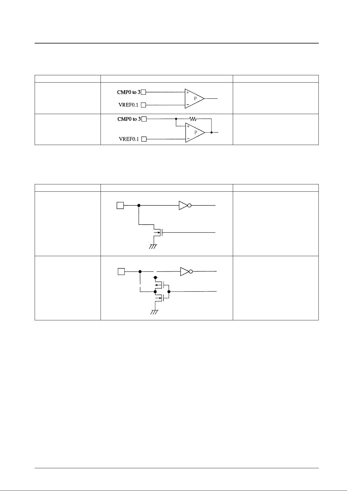
Comparator Options
The comparators offer the following two configuration options.
Port Output Configurations
The bidirectional I/O ports A, C, and D offer a choice of two output configurations.
No. 5117-8/39
LC6529N, LC6529F, LC6529L
Name Circuit diagram Conditions, etc.
Without feedback resistor
With feedback resistor
The comparator does not use hysteresis.
The comparator, in combination with an
external resistor, uses hysteresis.
Name Circuit diagram Conditions, etc.
Open drain (OD)
With pull-up resistors (PU)
This option adds a high-impedance pull-up
resistor for port A or D and a low-impedance
one for port C.
Specifications
LC6529N
Absolute Maximum Ratings at Ta = 25°C, VSS= 0 V
Note: 1. When the oscillator circuit in Figure 3 and the guaranteed constant are used, this is guaranteed over the full amplitude.
2. Averaged over 100-ms interval.
Allowable Operating Ranges at Ta = –40 to +85°C, VSS= 0 V, VDD= 3.0 to 6.0 V
Note: * Maintain the power supply voltage at VDDuntil the HALT instruction has completed execution, placing the chip in the standby mode. Block
chattering from entering PA3 during the HALT instruction execution cycle.
No. 5117-9/39
LC6529N, LC6529F, LC6529L
Parameter Symbol Conditions min typ max Unit
Maximum supply voltage V
DD
max V
DD
–0.3 +7.0 V
V
I
1 OSC1
*1
–0.3 VDD+ 0.3
Input voltage V
I
2 TEST, RES –0.3 VDD+ 0.3 V
V
I
3 Port E (PE) configuration –0.3 VDD+ 0.3
Output voltage V
O
OSC2 Voltages up to that generated allowed. V
I/O voltages
V
IO
1 Open-drain (OD) configuration –0.3 +15
V
V
IO
2 Pull-up (PU) resistor configuration –0.3 VDD+ 0.3
Peak output current I
OP
PA, PC, PD –2 +20 mA
I
OA
PA, PC, PD: Average for pin over 100-ms interval –2 +20
Average output current
ΣI
OA
1 PA: Total current for pins PA0 to PA3
*2
–6 +40
mA
ΣI
OA
2
PC, PD: Total current for pins PC0 to PC3 and
–14 +90
PD0 to PD3
*2
Pd max1 Ta = –40 to +85°C (DIP24S) 360
Allowable power dissipation Pd max2 Ta = –40 to +85°C (SSOP24) 165 mW
Pd max3 Ta = –40 to +85°C (MFP30S) 150
Operating temperature Topr –40 +85
°C
Storage temperature Tstg –55 +125
Parameter Symbol Conditions min typ max Unit
Supply voltage V
DD
V
DD
3.0 6.0 V
Standby voltage V
ST
VDD: Preserves contents of RAM and registers*. 1.8 6.0 V
V
IH
1
Open-drain (OD) configuration: With output N-channel
0.7 V
DD
13.5
transistor off
VIH2
Pull-up (PU) resistor configuration: With output
0.7 V
DD
V
DD
Input high level voltage
N-channel transistor off
V
V
IH
3 PE: Using port E configuration 0.7 V
DD
V
DD
VIH4 RES: VDD= 1.8 to 6 V 0.8 V
DD
V
DD
VIH5 OSC1: Using external clock option 0.8 V
DD
V
DD
VIL1
PA, PC, PD: With output N-channel transistor off,
V
SS
0.3 V
DD
VDD= 4 to 6 V
V
IL
2 PA, PC, PD: With output N-channel transistor off V
SS
0.25 V
DD
VIL3 PE: Using port E configuration, VDD= 4 to 6 V V
SS
0.3 V
DD
VIL4 PE: Using port E configuration V
SS
0.25 V
DD
Input low level voltage
V
IL
5 OSC1: Using external clock option, VDD= 4 to 6 V V
SS
0.25 V
DD
V
VIL6 OSC1: Using external clock option V
SS
0.2 V
DD
VIL7 TEST: VDD= 4 to 6 V V
SS
0.3 V
DD
VIL8 TEST V
SS
0.25 V
DD
VIL9 RES: VDD= 4 to 6 V V
SS
0.25 V
DD
VIL10 RES V
SS
0.2 V
DD
Operating frequency fop Using the built-in 1/3 or 1/4 frequency dividers extends
200 (20) 1444 (2.77) kHz (µs)
(cycle time) (Tcyc) the maximum to 4.33 MHz.
Continued on next page.
Continued from preceding page.
Electrical Characteristics at Ta = –40 to +85°C, VSS= 0 V, VDD= 3.0 to 6.0 V
Note: * The RC oscillator and external clock options require a Schmidt trigger configuration for OSC1.
No. 5117-10/39
LC6529N, LC6529F, LC6529L
Parameter Symbol Conditions min typ max Unit
[External clock conditions]
Frequency text 200 4330 kHz
Pulse width textH, textL 69
ns
Rise/fall times textR, textF 50
[Oscillator guaranteed constants]
Cext OSC1, OSC2: V
DD
= 4 to 6 V, Figure 2 220 ± 5%
pF
2-pin RC oscillator circuit
Cext OSC1, OSC2: Figure 2 220 ± 5%
Rext OSC1, OSC2: V
DD
= 4 to 6 V, Figure 2 4.7 ± 1%
kΩ
Rext OSC1, OSC2: Figure 2 12.0 ± 1%
Ceramic oscillator Figure 3 See Table 1.
OSC1: If the clock frequency exceeds 1.444 MHz, use
the built-in 1/3 or 1/4 frequency divider. Figure 1
Parameter Symbol Conditions min typ max Unit
Open-drain (OD) configuration for port: With output
IIH1 N-channel transistor off. (Includes transistor’s leak 5.0
Input high level current
current.) V
IN
= 13.5 V
µA
I
IH
2 PE: Using port E configuration, VIN= V
DD
1.0
I
IH
3 OSC1: Using external clock option, VIN= V
DD
1.0
Open-drain (OD) configuration for port: With output
IIL1 N-channel transistor off. (Includes transistor’s leak –1.0
current.) V
IN
= V
SS
µA
Pull-up (PU) resistor configuration for port A or D:
I
IL
2 With output N-channel transistor off. (Includes –220 –71.5
transistor’s leak current.) V
IN
= V
SS
Input low level current
Pull-up (PU) resistor configuration for port C:
I
IL
3 With output N-channel transistor off. (Includes –6.00 –2.17 mA
transistor’s leak current.) V
IN
= V
SS
IIL4 PE: Using port E configuration, VIN= V
SS
–1.0
I
IL
5 RES: VIN= V
SS
–45 –10 µA
I
IL
6 OSC1: Using external clock option, VIN= V
SS
–1.0
V
OH
1
Pull-up (PU) resistor configuration for port C:
VDD– 1.2
Output high level voltage
I
OH
= –300 µA, VDD= 4 to 6 V
V
V
OH
2
Pull-up (PU) resistor configuration for port C:
VDD– 0.5
I
OH
= –60 µA
V
OL
1 PA, PC, PD: IOL= 10 mA, VDD= 4 to 6 V 1.5
Output low level voltage
V
OL
2
PA, PC, PD: With I
OL
for each port less than or equal
0.4
V
to 1 mA, I
OL
= 1.8 mA
Hysteresis voltage
V
HIS
1 RES 0.1 V
DD
V
V
HIS
2 OSC1*: Using RC oscillator or external clock option 0.1 V
DD
Note:** f
CFOSC
is the allowable oscillator frequency.
Comparator Characteristics for Comparator Option at Ta = –40 to +85°C, VSS= 0 V, VDD= 3.0 to 6.0 V
No. 5117-11/39
LC6529N, LC6529F, LC6529L
Parameter Symbol Conditions min typ max Unit
[Current drain]
RC oscillator
I
DD OP
1 VDD: Figure 2, 850 kHz (typ) 0.8 2.0
mA
I
DD OP
2 VDD: Figure 2, 400 kHz (typ) 0.4 1.0
I
DD OP
3 VDD: Figure 3, 4 MHz, 1/3 frequency divider 1.6 4.0
I
DD OP
4 VDD: Figure 3, 4 MHz, 1/4 frequency divider 1.6 4.0
Ceramic oscillator
I
DD OP
5 VDD: Figure 3, 2 MHz, 1/3 frequency divider 1.3 3.0
mA
I
DD OP
6 VDD: Figure 3, 2 MHz, 1/4 frequency divider 1.3 3.0
I
DD OP
7 VDD: Figure 3, 800 kHz 1.1 2.6
I
DD OP
8 VDD: Figure 3, 400 kHz 0.9 2.4
V
DD
: 200 to 667 kHz, 1/1 frequency divider,
I
DD OP
9 600 to 2000 kHz, 1/3 frequency divider, 1.0 2.5
External clock
800 to 2667 kHz, 1/4 frequency divider
mA
VDD: 200 to 1444 kHz, 1/1 frequency divider,
I
DD OP
10 600 to 4330 kHz, 1/3 frequency divider, 1.6 4.2
800 to 4330 kHz, 1/4 frequency divider
I
DD
st1
V
DD
: With output N-channel transistor off and
0.05 10
Standby operation
port level = V
DD
, VDD= 6 V
µA
I
DD
st2
V
DD
: With output N-channel transistor off and
0.025 5
port level = V
DD
, VDD= 3 V
[Oscillator characteristics] (RC oscillator)
OSC1, OSC2: Figure 2, Cext = 220 pF ± 5%,
309 400 577
Oscillator frequency f
MOSC
Rext = 12.0 kΩ ± 1%
kHz
OSC1, OSC2: Figure 2, Cext = 220 pF ± 5%,
660 850 1229
Rext = 4.7 kΩ ± 1%, V
DD
= 4 to 6 V
[Oscillator characteristics] (Ceramic oscillator)
OSC1, OSC2: Figure 3, f
O
= 400 kHz 384 400 416
Oscillator frequency f
CFOSC
*
OSC1, OSC2: Figure 3, f
O
= 800 kHz 768 800 832
kHz
OSC1, OSC2: Figure 3, f
O
= 2 MHz 1920 2000 2080
OSC1, OSC2: Figure 3, f
O
= 4 MHz 3840 4000 4160
Figure 4, f
O
= 400 kHz 10
Oscillator stabilization interval t
CFS
Figure 4, fO= 800 kHz, fO= 2 MHz, fO= 4 MHz,
10
ms
1/3, 1/4 frequency divider
[Pull-up resistors]
Pull-up (PU) resistor configuration for port A or D:
RPP1 With output N-channel transistor off and VIN= VSS, 30 70 130
I/O ports
V
DD
= 5 V
Pull-up (PU) resistor configuration for port C:
kΩ
RPP2 With output N-channel transistor off and VIN= VSS, 1.0 2.3 3.9
V
DD
= 5 V
Reset port Ru RES: V
IN
= VSS, VDD= 5 V 200 500 725
External reset characteristic:
t
RST
See
Reset time Figure 6.
Pin capacitance C
P
f = 1 MHz, VIN= VSSfor pins other than one
10 pF
being measured
Parameter Symbol Conditions min typ max Unit
Reference input voltage range V
RFIN
V
REF
0 and V
REF
1 VSS+ 0.3 VDD– 1.5 V
Inphase input voltage range V
CMIN
CMP0 to CMP3 V
SS
VDD– 1.5 V
Offset voltage V
OFF
V
CMIN
= VSSto VDD– 1.5 V ±50 ±300 mV
Response speed
TRS1 Figure 5: V
DD
= 4 to 6 V 1.0 5.0
µs
TRS2 Figure 5 1.0 200
Input high level current
I
IH
1 V
REF
0 and V
REF
1 1.0
µA
I
IH
2 CMP0 to CMP3: Without feedback resistor option 1.0
Input low level current
I
IL
1 V
REF
0 and V
REF
1 –1.0
µA
I
IL
2 CMP0 to CMP3: Without feedback resistor option –1.0
Feedback resistor RCMFB CMP0 to CMP3: With feedback resistor option 460 kΩ
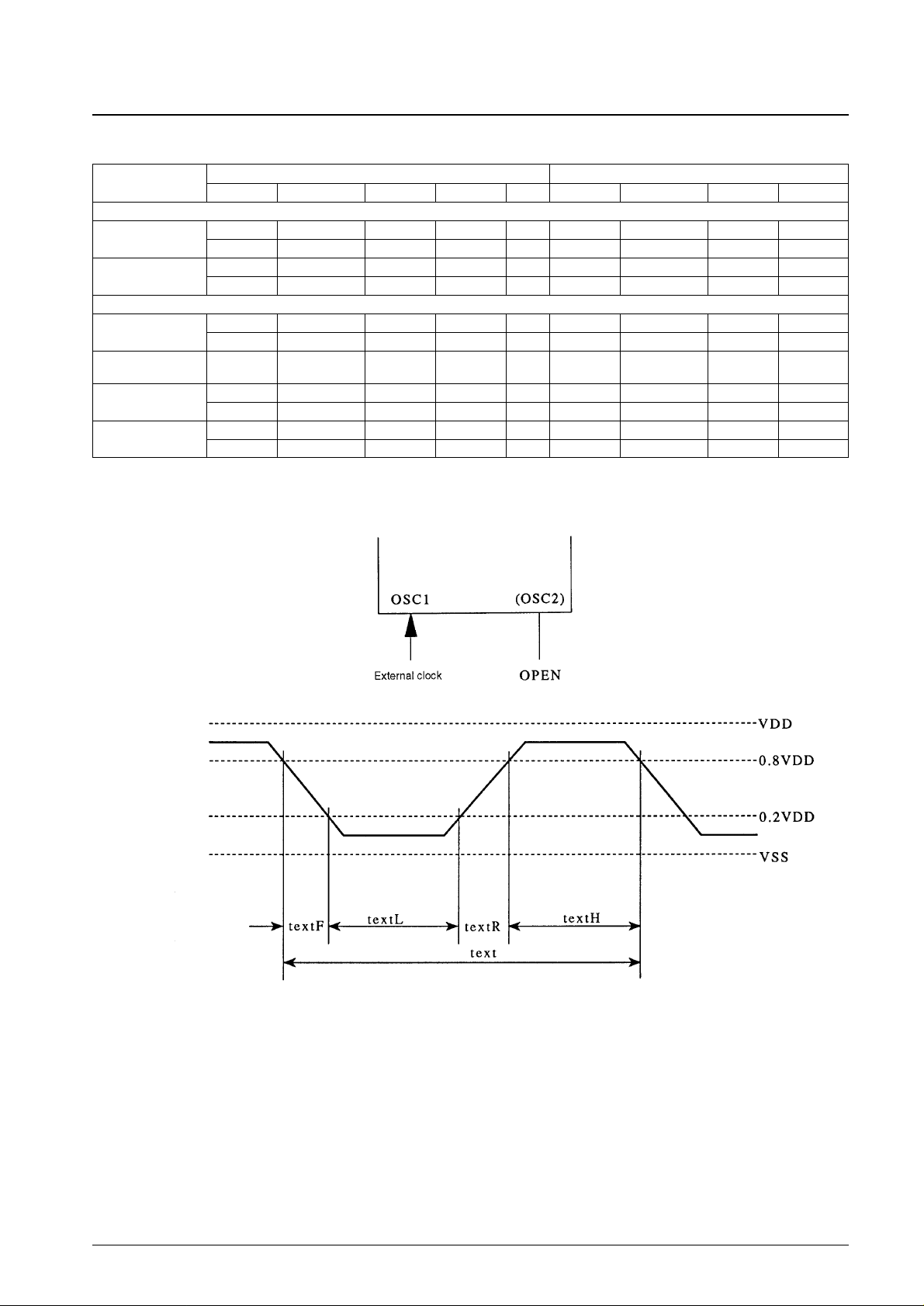
Table 1 Guaranteed Constants for Ceramic Oscillators
Figure 1 External Clock Input Waveform
No. 5117-12/39
LC6529N, LC6529F, LC6529L
Standard type Chip type
Oscillator type
Manufacturer Oscillator C1 C2 Rd Manufacturer Oscillator C1 C2
[External capacitor]
4-MHz ceramic
Murata CS A4.00MG 33 pF ±10% 33 pF ± 10% — Murata CS AC4.00MGC 33 pF ± 10% 33 pF ± 10%
oscillator
Kyocera KBR-4.0MSA 33 pF ± 10% 33 pF ± 10% — — — — —
2-MHz ceramic
Murata CS A2.00MG 33 pF ± 10% 33 pF ± 10% — Murata CS AC2.00MGC 33 pF ± 10% 33 pF ± 10%
oscillator
Kyocera KBR-2.0MSA 33 pF ± 10% 33 pF ± 10% — — — — —
[Built-in capacitor]
4-MHz ceramic
Murata CS A4.00MG — — — Kyocera KBR-4.0MWS — —
oscillator
Kyocera KBR-4.0MSA — — — — — — —
2-MHz ceramic
Murata CS A2.00MG — — — Kyocera KBR-2.0MWS — —
oscillator
800-kHz ceramic
Murata CS B800J
100 pF ± 10% 100 pF ± 10%
3.3 kΩ — — — —
oscillator
Kyocera KBR-800F/Y
150 pF ± 10% 150 pF ± 10%
— — — — —
400-kHz ceramic
Murata CS B400P
220 pF ± 10% 220 pF ± 10%
3.3 kΩ — — — —
oscillator
Kyocera KBR-400BK/Y
330 pF ± 10% 330 pF ± 10%
— — — — —
 Loading...