

Ordering number : ENN6498
40700RM (OT) No. 6498-1/39
Overview
The LC651431N/F/L and LC651432N/F/L are the smallscale control models in Sanyo’s LC6500 Series of 4-bit
microcontrollers and feature the same basic architecture
and instruction set. These microcontrollers are appropriate
for a wide range of applications, from applications that
require only a limited number of circuits and controls and
were previously implemented in standard logic to larger
application such as audio equipment, including tape decks
and disc players, office equipment, communication
equipment, automotive equipment, and home appliances.
Furthermore, since these products have equivalent basic
functions (although there are differences in some functions
and characteristics) and are pin compatible with the earlier
LC6543N/F/L and LC6546N/F/L products, they can be
used to replace those devices.
Features
• Fabricated in a CMOS process for low power operation
(Standby mode can be controlled by CPU instructions.)
• ROM/RAM
LC651432N/F/L
—ROM: 2 K × 8 bits, RAM: 128 × 4 bits
LC651431N/F/L
—ROM: 1 K × 8 bits, RAM: 64 × 4 bits
• Instruction set: The 80-instruction set common to the
whole LC6500 Series
• Wide operating supply voltage range of 2.2 to 6.0 V
(L versions)
• Instruction cycle time of 0.92 µs (F versions)
• On-chip serial I/O function
• Highly flexible I/O ports
Number of ports
— 7 ports (Up to 25 pins)
All ports
— Can be used for either input or output
— Voltage handling capability (input and output):
15 V maximum (For open-drain specification ports)
— Output current: 20 mA maximum sink current
(Capable of directly driving an LED.)
I/O port options to match application requirements:
— Open-drain output and pull-up resistor specification:
Can be specified for all ports in bit units.
— Output level at reset specification: Either a high or
low level can be specified for ports C and D in 4-bit
units each.
• Interrupts
Timer overflow vector interrupt (can also be tested by
CPU instructions)
INT pin or serial I/O full/empty vector interrupt (can
also be tested by CPU instructions)
• Stack levels: 4 levels (also used by interrupts)
• Timers: 8-bit programmable timer with 4-bit prescaler
• Clock oscillator options to match application
requirements:
Oscillator circuit option:
— Two-pin RC oscillator (N and L versions)
Two-pin ceramic oscillator or single external clock
input pin (N, F, and L versions)
— Divider circuit option: No divider, built-in divide-
by-three circuit, built-in divide-by-four circuit
(N and L versions)
• Continuous square-wave output with a period 64 times
the cycle time.
LC651432N/F/L, 651431N/F/L
SANYO Electric Co.,Ltd. Semiconductor Company
TOKYO OFFICE Tokyo Bldg., 1-10, 1 Chome, Ueno, Taito-ku, TOKYO, 110-8534 JAPAN
Four-Bit CMOS Microcontrollers for
Small-Scale Control Applications
CMOS IC
Any and all SANYO products described or contained herein do not have specifications that can handle
applications that require extremely high levels of reliability, such as life-support systems, aircraft’s
control systems, or other applications whose failure can be reasonably expected to result in serious
physical and/or material damage. Consult with your SANYO representative nearest you before using
any SANYO products described or contained herein in such applications.
SANYO assumes no responsibility for equipment failures that result from using products at values that
exceed, even momentarily, rated values (such as maximum ratings, operating condition ranges, or other
parameters) listed in products specifications of any and all SANYO products described or contained
herein.

No. 6498-2/39
LC651432N/F/L, 651431N/F/L
(1.04)
1.78
0.95
0.48
10.16
3.95max
(3.25)
0.51min
3.0
0.25
115
30 16
8.6
27.0
SANYO: DIP30SD
[LC651432N/F/L, 651431N/F/L]
Package Dimensions
unit : mm
3196A-DIP30SD
115
16
7.6
0.65
9.75
0.5
5.6
0.1
1.5max
30
0.22
(0.33)
0.15
(1.3)
SANYO: SSOP30
[LC651432N/F/L, 651431N/F/L]
unit : mm
3191A-SSOP30
0.15
15.2
115
30 16
(0.6)
1.00.4
2.45max
(2.15)
0.1
0.65
7.9
10.5
SANYO: MFP30S
[LC651432N/F/L, 651431N/F/L]
unit : mm
3216B-MFP30S
No. 6498-3/39
LC651432N/F/L, 651431N/F/L
Function Overview
Parameter LC651432N/1431N LC651432F/1431F LC651432L/1431L
ROM
2048 × 8 bits (1432N/F/L)
Memory
1024 × 8 bits (1431N/F/L)
RAM
128 × 4 bits (1432N/F/L)
64 × 4 bits (1431N/F/L)
Instructions
Instruction set 80
Table reference Provided
Interrupts One external, one internal
Timers 8-bit timer with 4-bit prescaler
On-chip functions Stack levels 4
HALT instruction based
Standby function standby function
Provided
Number of ports Up to 25 I/O pins
Serial ports I/O in 4-bit or 8-bit units
I/O voltage 15 V max.
I/O ports Output current 10 mA typ. 20 mA max.
I/O circuit types Open drain (n channel) or built-in pull-up resistor output can be specified in 1-bit units.
Output level at reset High or low can be specified in port units (C and D ports only)
Square-wave output Possible
Minimum cycle time 2.77 µs (V
DD
≥ 3 V) 0.92 µs (VDD≥ 3 V) 3.84 µs (VDD≥ 2.2 V)
Characteristics Supply voltage 3 to 6 V 3 to 6 V 2.2 to 6 V
Supply current 1 mA typ. 1.5 mA typ. 1 mA typ.
RC oscillator (400 or 800 kHz typical)
RC oscillator (400 kHz typical)
Oscillator
Oscillator element Ceramic oscillator (400 kHz, Ceramic oscillator: 4 MHz Ceramic oscillator (400 kHz
800 kHz, 1 MHz, or 4 MHz) or 4 MHz)
Divider circuit option 1/1, 1/3, 1/4 1/1 1/1, 1/3, 1/4
Other features Package
DIP30S-D, MFP30S,
SSOP30
Note: Sanyo will be providing details on oscillator elements and oscillator circuit constants as recommended circuits are developed. Contact your Sanyo
representative for more information.

No. 6498-4/39
LC651432N/F/L, 651431N/F/L
Differences between the LC651432N/LC651431N and the LC6543N/LC6546N
This table lists the points that require care when replacing the LC6543N/LC6546N with the LC651432N/LC651431N in
completes end products.
Parameter LC651432N/1431N LC6543N/46N
Pdmax(1) : DIP 310 mW 250 mW
Allowable power dissipation Pdmax(2) : MFP 220 mW 150 mW
Pdmax(3) : SSOP 160 mW (This package not available.)
I/O voltage (PIO) V
IO
(3) added –0.3 to VDD+ 0.3
–0.3 to +15 V
(When open-drain output is used.)
–0.3 to VDD+ 0.3
(When a pull-up resistor is used.)
VIH(1) to VIH(7)
High-level input voltage V
IH
(n) (Associated with the I/O voltage (PI0) VIH(1) to VIH(6)
changes mentioned above.)
IIH(1) to IIH(3)
High-level input current I
IH
(n) (Associated with the I/O voltage (PI0) IIH(1) to IIH(2)
changes mentioned above.)
f
CFOSC
Oscillator frequency precision: ±2%
[OSC1, OSC2]
Recommended oscillator circuit constants Oscillator frequency precision: ±4%
Oscillator characteristics
(under evaluation)
Ceramic oscillator
800 kHz typical (V
DD
= 3 to 6 V) 850 kHz typical (VDD= 4 to 6 V)
Oscillator frequency
Circuit constant changes: Rext = 6.8 kΩ ±1% Circuit constant changes: Rext = 4.7 kΩ ±1%
2-pin RC oscillator f
MOSC
Sample-to-sample frequency variation: Sample-to-sample frequency variation:
Oscillator frequency [OSC1, OSC2]
595 to 1274 kHz 619 to 1144 kHz
400 kHz typical (VDD= 3 to 6 V) 400 kHz typical (VDD= 3 to 6 V)
Sample-to-sample frequency variation: Sample-to-sample frequency variation:
284 to 790 kHz 305 to 546 kHz
Current drain I
DD
1 mA typ. 2 mA typ.
Serial clock input clock cycle time t
CKCY
(1)[SCK] min. 2.0 µs min 3.0 µs
Package
DIP30S-D, MFP30S,
DIP30S-D, MFP30S
SSOP30 added
Differences between the LC651432F/LC651431F and the LC6543F/LC6546F
This table lists the points that require care when replacing the LC6543F/LC6546F with the LC651432F/LC651431F in
completes end products.
Parameter LC651432F/1431F LC6543F/46F
Pdmax(1) : DIP 310 mW 250 mW
Allowable power dissipation Pdmax(2) : MFP 220 mW 150 mW
Pdmax(3) : SSOP 160 mW (This package not available.)
Operating supply voltage V
DD
3 to 6 V 4.5 to 6 V
I/O voltage (PI0) V
IO
(3) added –0.3 to VDD+ 0.3
–0.3 to +15 V
(When open-drain output is used.)
–0.3 to VDD+ 0.3
(When a pull-up resistor is used.)
VIH(1) to VIH(7)
High-level input voltage V
IH
(n) (Associated with the I/O voltage (PI0) VIH(1) to VIH(6)
changes mentioned above.)
IIH(1) to IIH(3)
High-level input current I
IH
(n) (Associated with the I/O voltage (PI0) IIH(1) to IIH(2)
changes mentioned above.)
IIH(1) to IIH(3)
Low-level input voltage V
IL
(n) Specifications when VDD= 4 to 6 V Specifications when VDD= 4 to 6 V
Specifications added for V
DD
= 3 to 6 V
Oscillator characteristics
f
CFOSC
Ceramic oscillator
[OSC1, OSC2]
Oscillator frequency precision: ±2% Oscillator frequency precision: ±4%
Oscillator frequency
Current drain I
DD
1.5 mA typ. 2.5 mA typ.
Serial clock input clock cycle time t
CKCY
(1)[SCK] min. 2.0 µs min 3.0 µs
Package
DIP30S-D, MFP30S,
DIP30S-D, MFP30S
SSOP30 added
No. 6498-5/39
LC651432N/F/L, 651431N/F/L
Differences between the LC651432L/LC651431L and the LC6543L/LC6546L
This table lists the points that require care when replacing the LC6543L/LC6546L with the LC651432L/LC651431L in
completes end products.
Parameter LC651432L/1431L LC6543L/46L
Pdmax(1) : DIP 310 mW 250 mW
Allowable power dissipation Pdmax(2) : MFP 220 mW 150 mW
Pdmax(3) : SSOP 160 mW (This package not available.)
I/O voltage (PI0) V
IO
(3) added –0.3 to VDD+ 0.3
–0.3 to +15 V
(When open-drain output is used.)
–0.3 to VDD+ 0.3
(When a pull-up resistor is used.)
VIH(1) to VIH(7)
High-level input voltage V
IH
(n) (Associated with the I/O voltage (PI0) VIH(1) to VIH(6)
changes mentioned above.)
IIH(1) to IIH(3)
High-level input current I
IH
(n) (Associated with the I/O voltage (PI0) IIH(1) to IIH(2)
changes mentioned above.)
f
CFOSC
Oscillator frequency precision: ±2%
Oscillator characteristics
[OSC1, OSC2]
Recommended oscillator circuit constants Oscillator frequency precision: ±4%
Ceramic oscillator
(under evaluation)
Oscillator frequency 400 kHz typical (V
DD
= 2.2 to 6 V) 400 kHz typical (VDD= 2.2 to 6 V)
2-pin RC oscillator f
MOSC
Circuit constant changes: Rext = 15 kΩ ±1% Circuit constant changes: Rext = 12 kΩ ±1%
Oscillator frequency [OSC1, OSC2] Sample-to-sample frequency variation: Sample-to-sample frequency variation:
200 to 790 kHz 284 to 546 kHz
Current drain I
DD
1 mA typ. 2 mA typ.
Package
DIP30S-D, MFP30S,
DIP30S-D, MFP30S
SSOP30 added
Caution: Always test the end product thoroughly after changing the microcontroller used.
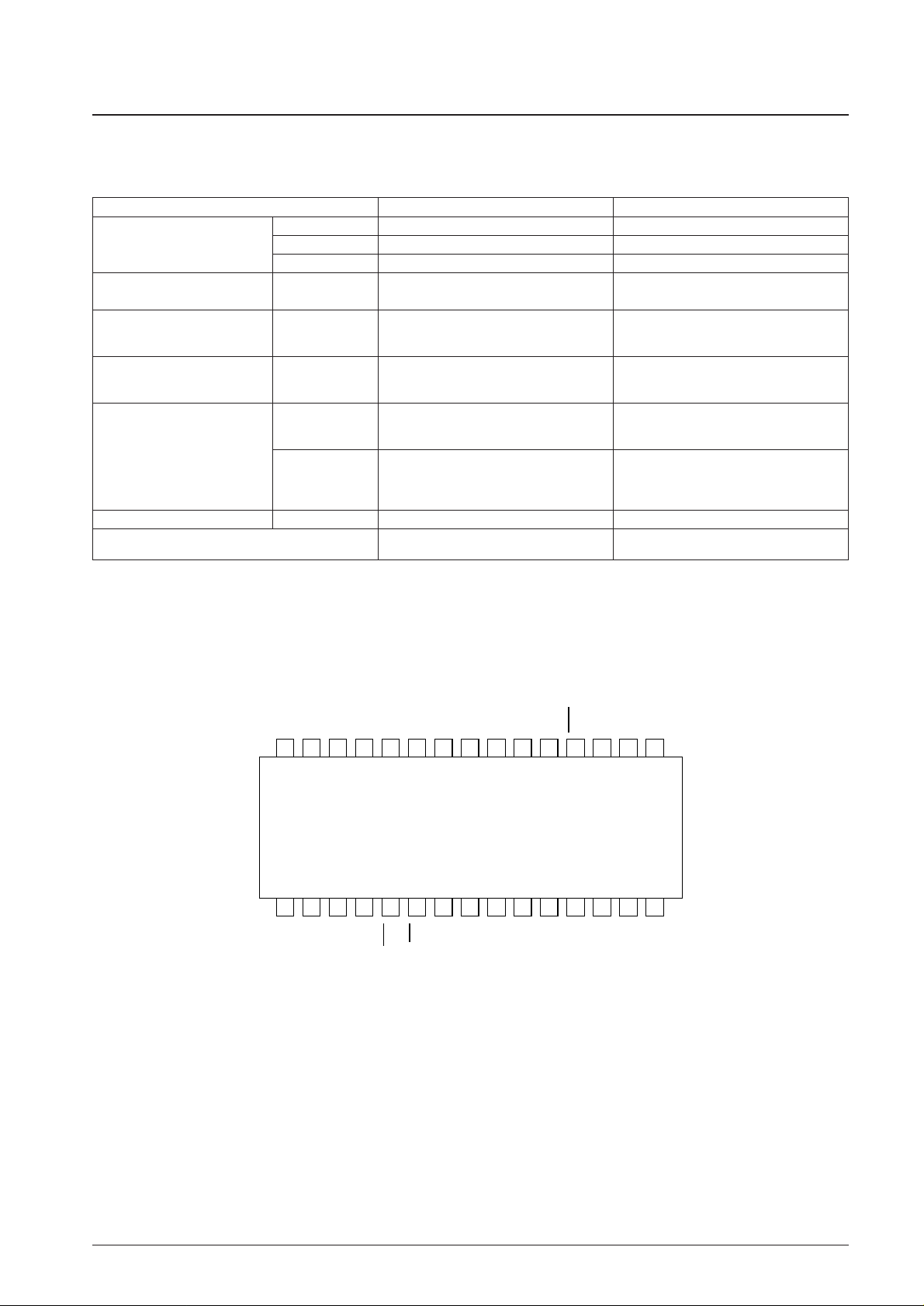
Pin Assignment
The same pin assignment is used for the DIP, MFP, and SSOP packages.
RES
30
29
28
27
26
25
24
23
22
21
20
19
18
17
16
PE2
PE1
PE0
PD3
PD2
PD1
PD0
PC3
PC2
PC1
PC0
VSS
TEST
OSC1
PA1
PE3
VDD
PF0/SI
PF1/SO
PF2/SCK
PF3/INT
PG0
PG1
PG2
PG3
PA0
PA2
PA3
PI0/OSC2
12
1
2
3
4
5
6
7
8
9
10
11
13
14
15
LC651432N/F/L
LC651431N/F/L
Pin Nomenclature
OSC1, OSC2: Connections for capacitor and resistor oscillator components or a ceramic oscillator element.
PG0 to 3: Shared-function I/O port G0 to 3 PI0: Shared-function I/O port IO
RES: Reset TEST:Test
PA0 to 3: Shared-function I/O port A0 to 3 INT: Interrupt request
PC0 to 3: Shared-function I/O port C0 to 3 SI: Serial input
PD0 to 3: Shared-function I/O port D0 to 3 SO: Serial output
PE0 to 3: Shared-function I/O port E0 to 3 SCK: Serial clock input or output pin
PF0 to 3: Shared-function I/O port F0 to 3
Notes: 1. The SI, SO, SCK, and INT pins are shared-function pins also used as PF0 to 3.
2. OSC2 and PIO are a single pin set exclusively to one or the other function as a user option.
Note: * OSC2 and PIO are a single pin set exclusively to one or the other function as a user option.
RAM: Data memory ROM: Program memory
F: Flags PC: Program counter
WR: Working register INT: Interrupt control
AC: Accumulator IR: Instruction register
ALU: Arithmetic and logic unit I.DEC: Instruction decoder
DP: Data pointer CF, CSF: Carry flag, carry save flag
E: E register ZF, ZSF: Zero flag, zero save flag
CTL: Control register EXTF: External interrupt request flag
OSC: Oscillator circuit TMF: Internal interrupt request flag
TM: Timer
STS: Status register
No. 6498-6/39
LC651432N/F/L, 651431N/F/L
LC651432N/F/L, LC651431N/F/L
Port A
Port C
Port D
Port E
Port F
Serial
shift
register
Serial
shift
register
Port G Port I
Serial
mode
register
Serial
mode
register
I/O buffer
RAM
I.DEC
E AC
ALU
CF
EXTF TMF
CSF ZSF
TM
CTL
INT
OSC
System bus
STS
DP
PA0 to 3
PC0 to 3
PD0 to 3
PE0 to 3
PF0 to 3
I/O bus
OSC1
OSC2*
IR
ROM
PC
STACK 1
STACK 2
STACK 3
STACK 4
RES
TEST
V
DD
V
SS
PF1/SO
Shared with port F
4/8 bits
4 bits
Lower digit
Higher
4/8 bits
PF0/SI
PF2/SCK
PF3/INT
FWR
PG0-3 PI0
*
ZF
System Block Diagram
Development Support
The following are available to support the development of LC651431 and LC651432 applications.
• User’s manual
“LC6543/46 User’s Manual” No. E71
• Development tool manual
See the “EVA86000 Development Tool Manual for 4-Bit Microcontrollers.”
• Software manual
“LC65/66 Series Software Manual”
• Development tools
Program development: EVA86000 System
Program evaluation: LC65E43 on-chip EPROM microcontroller
No. 6498-7/39
LC651432N/F/L, 651431N/F/L
Pins Functions
Count Pin I/O Function Options Reset state
Handling when
unused
1V
DD
— Power supply — — —
1V
SS
—
1 OSC1 Input • Connection for the external system clock 1. Single-pin external clock input — —
RC or ceramic oscillator element 2. 2-pin RC oscillator
• When a single pin is used for external clock 3. 2-pin ceramic oscillator
input, the PI0/OSC2 pin is used as the PI0 4. Divider circuit option
I/O port. • No divider
• When a 2-pin RC oscillator or a 2-pin ceramic • Divide-by-three circuit
oscillator is used, the PI0/OSC2 pin is used as • Divide-by-four circuit
the OSC2 oscillator pin.
4 PA0 to PA3 I/O • I/O port A0 to 3 1. Open-drain output • High-level The open-drain
Input in 4-bit units (IP instruction) 2. Built-in pull-up resistor output (with output option
Output in 4-bit units (OP instruction) Options 1 and 2 may be specified the output n- must be
Test in single-bit units (BP and BNP instructions) in bit units. channel selected and
Set/reset in single-bit units (SPB and RPB transistor off) the pin
instructions) connected to
• PA3 (Any one of PA0 to 3 can be selected) is V
SS
.
used for standby mode control.
• Applications must assure that key bounce or
similar noise does not occur on PA3
(or PA0 to 3)
during a HALT instruction execution cycle.
4 PC0 to PC3 I/O • I/O port C0 to 3 1. Open-drain output • High-level The same as
Provides the same functions as PA0 to 3. 2. Built-in pull-up resistor output
that for PC0 to 3
(See note.) 3. High-level output at reset • Low-level
• The output level at reset can be specified to be 4. Low-level output at reset output
either high or low. • Options 1 and 2 may be specified (Specified as a
Note: This port does not have the standby in bit units. user option.)
mode control function. • Options 3 and 4 are specified in
a single 4-bit group
4 PD0 to PD3 I/O • I/O port D0 to 3 The same as those for PC0 to 3. The same as The same as
Provides the same functions as PC0 to 3.
those for PC0 to 3. those for PC0 to 3.
Continued on next page.
No. 6498-8/39
LC651432N/F/L, 651431N/F/L
Continued from preceding page.
Count Pin I/O Function Options Reset state
Handling when
unused
4 PE0 to PE3 I/O • I/O port E0 to 3 1. Open-drain output • High-level The same as
Input in 4-bit units (IP instruction) 2. Built-in pull-up resistor output (with that for
Output in 4-bit units (OP instruction) Options 1 and 2 may be specified the output n- PA0 to 3.
Set/reset in single-bit units (SPB and RPB in bit units. channel
instructions) transistor off)
Test in single-bit units (BP and BNP instructions)
• PE0 also has a continuous pulse (64Tcyc)
output function.
4 PF0/SI I/O • I/O port F0 to 3 The same as those for PE0 to 3. The same as The same as
PF1/SO Functions and options identical to PE0 to 3. that for PE0 to 3. that for
PF2/SCK (See note.) The serial port PA0 to 3.
PF3/INT • PF0 to 3 have shared functions as the serial is disabled and
interface pins and the INT input. INT is the
Either function can be selected under program interrupt source.
control.
SI ... Serial input port
SO ... Serial output port
SCK ... Serial clock input or output
INT ... Interrupt request input
Serial input/output is switched between 4-bit
and 8-bit units under program control.
Note: This port does not have a continuous
pulse output function.
4 PG0 to PG3 I/O • I/O port G0 to 3 The same as those for PE0 to 3. The same as The same as
Functions and options identical to PE0 to 3. those for that for
(See note.) PE0 to 3. PA0 to 3.
Note: This port does not have a continuous
pulse output function.
1 PI0/OSC2 I/O • I/O port IO The same as those for PG0 to 3. The same as The same as
Output Functions and options identical to PG0 to 3. those for that for
• However, consists of a single bit. PG0 to 3. PA0 to 3.
• When a 2-pins oscillator is used, this pin
functions as the OSC2 pin, and the I/O port
function is not available.
1 RES Input • System reset input — — —
• Connect an external capacitor to implement a
power-on reset.
• The reset start operation requires that a low
level be held for at least 4 clock cycles.
1 TEST Input • IC test pin — — This pin must
This pin must be connected to V
SS
during be connected to
normal operation. V
SS
.
No. 6498-9/39
LC651432N/F/L, 651431N/F/L
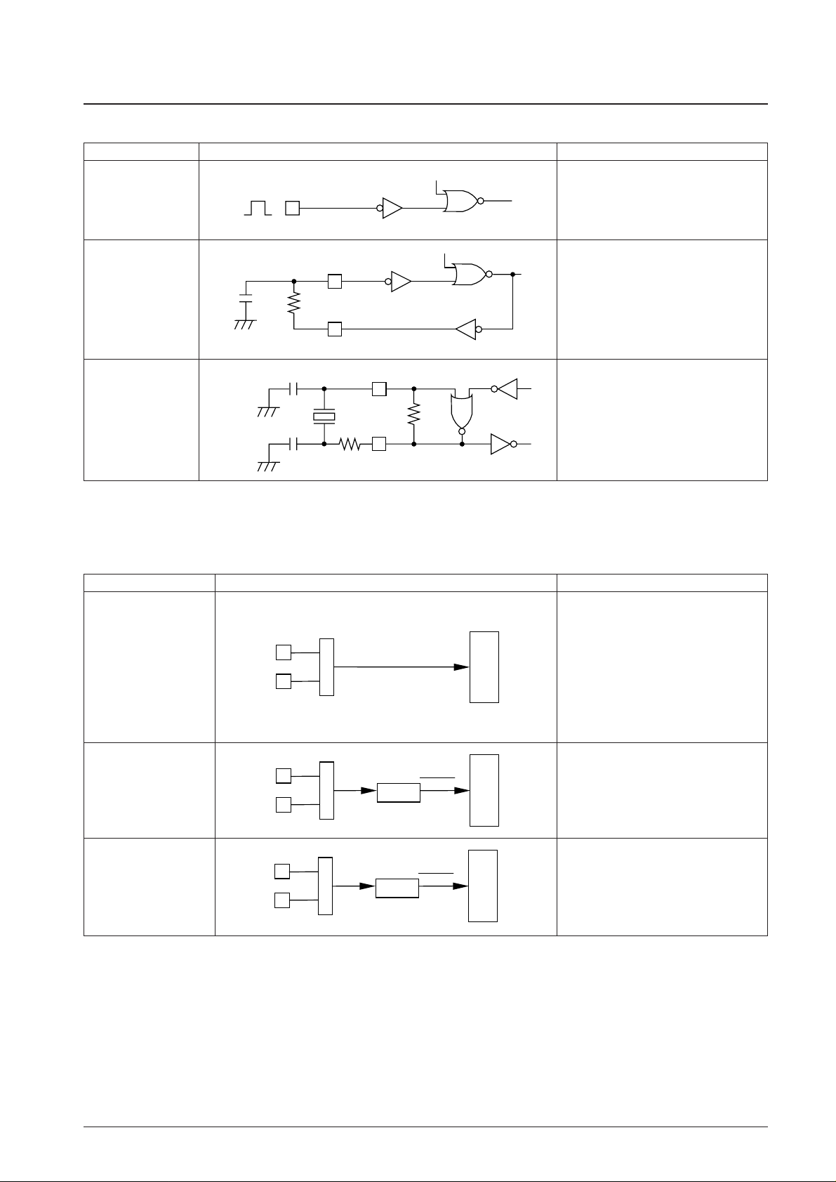
Oscillator Circuit Options
Option Circuit Conditions and notes
The PI0/OSC2 pin is used as the PI0 pin.External clock
OSC1
The PI0/OSC2 pin is used as the OSC2 pin
and the port function is unavailable.
Two-pin RC oscillator
OSC1
PI0/OSC
Rext
Cext
The PI0/OSC2 pin is used as the OSC2 pin
and the port function is unavailable.
Ceramic oscillator
OSC1
PI0/OSC
R
C1
C2
Ceramic oscillator
element
Divider Circuit Options
Option Circuit Conditions and notes
• Applicable to all three oscillator options.
• The oscillator frequency or the external clock
must not exceed 1444 kHz. (LC651431N and
LC651432N)
• The oscillator frequency or the external clock
must not exceed 4330 kHz. (LC651431F and
LC651432F)
• The oscillator frequency or the external clock
must not exceed 1040 kHz. (LC651431L and
LC651432L)
No divider circuit (1/1)
f
OSC
Oscillator circuit
Timing
generator
• Only applicable to the external clock and the
ceramic oscillator option.
• The oscillator frequency or the external clock
must not exceed 4330 kHz.
Divide-by-three circuit (1/3)
f
OSC
Divide-by-three
circuit
f
OSC
3
Oscillator circuit
Timing
generator
• Only applicable to the external clock and the
ceramic oscillator option.
• The oscillator frequency or the external clock
must not exceed 4330 kHz.
Divide-by-four circuit (1/4)
f
OSC
Divide-by-four
circuit
f
OSC
4
Oscillator circuit
Timing
generator
Caution: The following table summarizes the oscillator and divider option combinations. Use care when selecting these options.
Oscillator Divider Options for the LC651431N/LC651432N, LC651431F/LC651432F, and
LC651431L/LC651432L
No. 6498-10/39
LC651432N/F/L, 651431N/F/L
LC651432N, LC651431N
Oscillator type Frequency Divider option (cycle time) VDDrange Notes
Ceramic oscillator 400 kHz 1/1 (10 µs) 3 to 6 V The divide-by-three and divide-by-four
circuits cannot be used.
800 kHz 1/1 (5 µs) 3 to 6 V
1/3 (15 µs) 3 to 6 V
1/4 (20 µs) 3 to 6 V
1 MHz 1/1 (4 µs) 3 to 6 V
1/3 (12 µs) 3 to 6 V
1/4 (16 µs) 3 to 6 V
4 MHz 1/3 (3 µs) 3 to 6 V The no-divider (1/1) option cannot be used.
1/4 (4 µs) 3 to 6 V
Single-pin external clock input 200 to 1444 kHz 1/1 (20 to 2.77 µs) 3 to 6 V
600 to 4330 kHz 1/3 (20 to 2.77 µs) 3 to 6 V
800 to 4330 kHz 1/4 (20 to 3.70 µs) 3 to 6 V
External clock provided by a As above
2-pin RC oscillator circuit
2-pin RC oscillator Using the no-divider (1/1) option and the 3 to 6 V
recommended circuit constants. If the use of circuit
values other than the recommended values is unavoidable, the
frequencies, divider options, and V
DD
ranges specified for the
single-pin external clock input option must be strictly observed.
External clock used with the The IC cannot be driven by an external clock with this option. If external clock drive is required, select either the external
ceramic oscillator option clock option or the 2-pin RC oscillator option
LC651432F, LC651431F
Oscillator type Frequency Divider option (cycle time) VDDrange Notes
Ceramic oscillator 4 MHz 1/1 (1 µs) 3 to 6 V
Single-pin external clock input 200 to 4330 kHz 1/1 (20 to 0.92 µs) 3 to 6 V
External clock used with the The IC cannot be driven by an external clock with this option. If external clock drive is required, select the external clock
ceramic oscillator circuit option.
LC651432L, LC651431L
Oscillator type Frequency Divider option (cycle time) VDDrange Notes
Ceramic oscillator 400 kHz 1/1 (10 µs) 2.2 to 6 V The divide-by-three and divide-by-four
circuits cannot be used.
4 MHz 1/4 (4 µs) 2.2 to 6 V The no-divider (1/1) and divide-by-three option
cannot be used.
Single-pin external clock input 200 to 1040 kHz 1/1 (20 to 3.84 µs) 2.2 to 6 V
600 to 3120 kHz 1/3 (20 to 3.84 µs) 2.2 to 6 V
800 to 4160 kHz 1/4 (20 to 3.84 µs) 2.2 to 6 V
External clock provided by a As above
2-pin RC oscillator circuit
2-pin RC oscillator Using the no-divider (1/1) option and the 2.2 to 6 V
recommended circuit constants. If the use of circuit
values other than the recommended values is unavoidable, the
frequencies, divider options, and V
DD
ranges specified for the
single-pin external clock input option must be strictly observed.
External clock used with the The IC cannot be driven by an external clock with this option. If external clock drive is required, select either the external
ceramic oscillator option clock option or the 2-pin RC oscillator option
No. 6498-11/39
LC651432N/F/L, 651431N/F/L
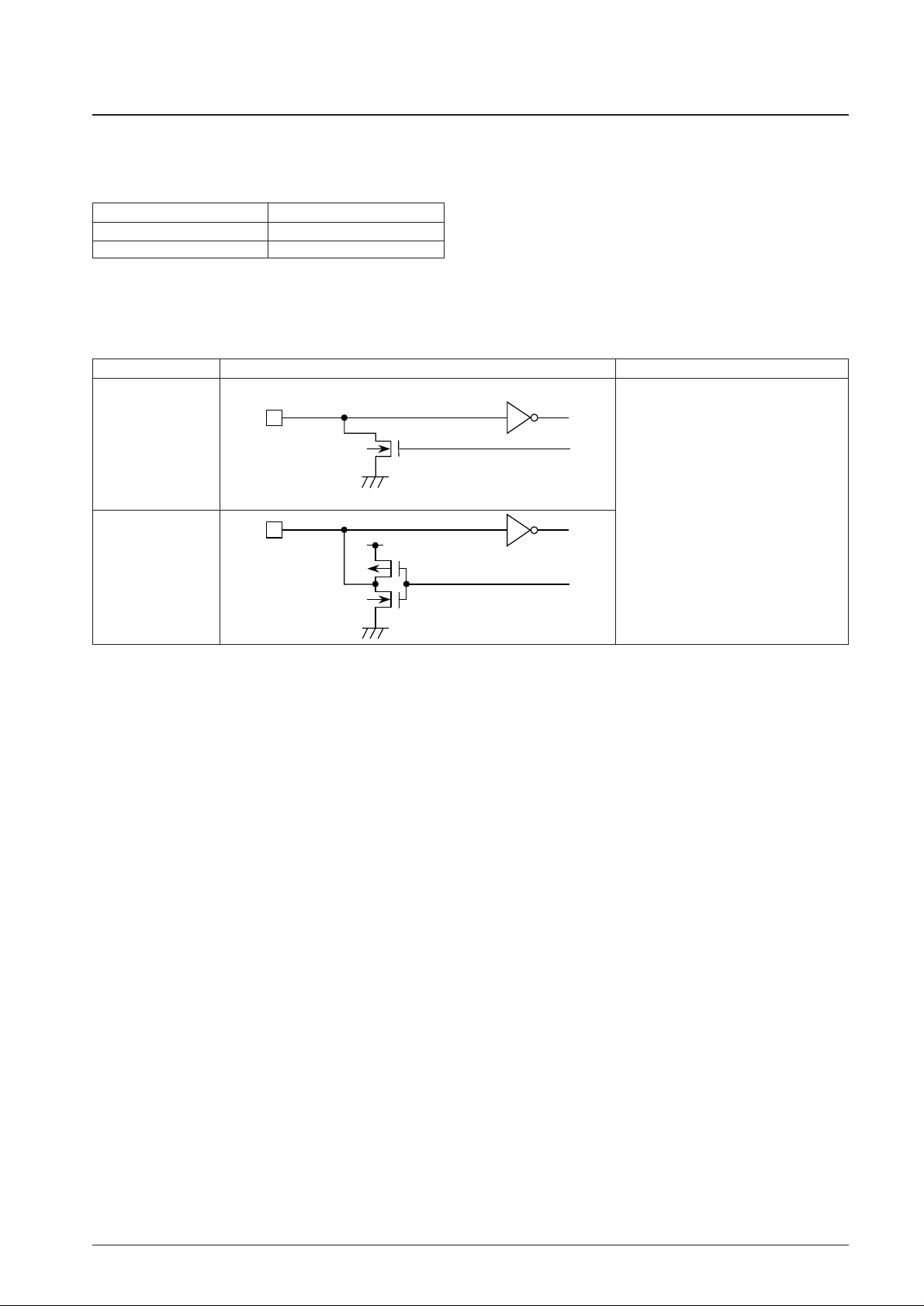
Port C and D Output Level at Reset Option
One of the following two options for the output level at reset may be chosen for the I/O ports C and D in 4-bit group
units.
Port Output Circuit Type Option
One of the following two options for the circuit type can be selected for the I/O ports in bit units.
Option Conditions and notes
High-level output at reset Ports C and D in 4-bit units
Low-level output at reset Ports C and D in 4-bit units
Option Circuit Applicable ports
• Not applicable to the PI0/OSC2 pin if either
the 2-pin RC oscillator or the ceramic
oscillator is selected as the oscillator circuit.
Open-drain output
Built-in pull-up resistor
output
Specifications
No. 6498-12/39
LC651432N/F/L, 651431N/F/L
Parameter Symbol Conditions Applicable pins Ratings Unit
Maximum supply voltage V
DD
max V
DD
–0.3 to +7.0 V
Voltages up to the
Output voltage V
O
OSC2 voltage generated V
are allowed.
Input voltage
VI(1) OSC1
*1
–0.3 to VDD+0.3 V
V
I
(2) TEST, RES –0.3 to VDD+0.3 V
V
IO
(1) Ports with open-drain specifications –0.3 to +15 V
I/O voltage
V
IO
(2)
Ports with pull-up resistor
–0.3 to VDD+0.3 V
specifications
V
IO
(3) PI0 –0.3 to VDD+0.3 V
Peak output current I
OP
I/O ports –2 to +20 mA
I
OA
Per single pin, the average over a
I/O ports –2 to +20 mA
100 ms period
The total current for PC0 to 3,
PC0 to 3
mA
Average output current
ΣI
OA
(1)
PD0 to 3, and PE0 to 3
*2
PD0 to 3 –15 to +100
PE0 to 3
The total current for PF0 to 3,
PF0 to 3, PI0
ΣI
OA
(2)
PG0 to 3, PA0 to 3, and PI0
*2
PG0 to 3 –15 to +100 mA
PA0 to 3
Pd max(1) Ta = –40 to +85°C (DIP package) 310 mW
Allowable power dissipation Pd max(2) Ta = –40 to +85°C (MFP package) 220 mW
Pd max(3) Ta = –40 to +85°C (SSOP package) 160 mW
Operating temperature Topr –40 to +85 °C
Storage temperature Tstg –55 to 125 °C
LC651432N, 651431N
Absolute Maximum Ratings at Ta = 25°C, VSS= 0 V
Parameter Symbol Conditions Applicable pins
Ratings
Unit
min typ max
Operating supply voltage V
DD
V
DD
3.0 6.0 V
Standby supply voltage V
ST
RAM and register contents
V
DD
1.8 6.0 V
retained.
*3
VIH(1)
With the n-channel output Ports with open-drain
0.7 V
DD
13.5 V
transistors off specifications (except for I0)
VIH(2)
With the n-channel output Ports with pull-up resistor
0.7 V
DD
V
DD
V
transistors off specifications (except for I0)
VIH(3)
With the n-channel output
Port I0 0.7 V
DD
V
DD
V
transistors off
High-level input voltage
VIH(4)
With the n-channel output The INT, SCK, and SI pins
0.8 V
DD
13.5 V
transistors off with open-drain specifications
With the n-channel output
The INT, SCK, and SI pins
V
IH
(5)
transistors off
with pull-up resistor 0.8 V
DD
V
DD
V
specifications
VIH(6) VDD= 1.8 to 6 V RES 0.8 V
DD
V
DD
V
V
IH
(7) External clock specifications OSC1 0.8 V
DD
V
DD
V
Allowable Operating Ranges at Ta = –40 to +85°C, VSS= 0 V, VDD= 3.0 to 6.0 V (unless otherwise specified)
Continued on next page.
 Loading...