

Ordering number : ENN*6727
LC651306A/04A/02A/01A
4-Bit Single-Chip Microcontroller
for Small-Scale Control Applications
Preliminary
Overview
The LC651306A, LC651304A, LC651302A, LC651301A belong to our 4-bit single-chip microcontroller LC6500 series
fabricated using CMOS process technology. They are ideally suited for use in small-scale control applications. Their basic
architecture and instruction set are the same. These microcontrollers include an 8-input 8-bit A/D converter and are
appropriate for use in a wide range of applications. That range includes applications with a small number of control circuits
that were previously implemented in standard logic, and applications with a larger scale such as home appliances,
automotive equipment, communications equipment, office equipment, and audio equipment such as decks and players.
Features
1) CMOS technology for a low-power consumption operation (A standby function that can be invoked under program
control is also provided.)
2) ROM/RAM
LC651306A ROM : 6K × 8 bits, RAM : 256 × 4 bits
LC651304A ROM : 4K × 8 bits, RAM : 256 × 4 bits
LC651302A ROM : 2K × 8 bits, RAM : 256 × 4 bits
LC651301A ROM : 1K × 8 bits, RAM : 256 × 4 bits
3) Instruction set : 81 instructions common to all microcontrollers of the LC6500 series
4) Wide operating voltage range : 2.5V to 6.0V
5) Instruction cycle time : 0.92 µs
6) On-chip serial I/O port
CMOS IC
Ver.0.90
62600
91400 RM (IM) TY No.6727-1/21

LC651306A/04A/02A/01A
7) Flexible I/O port
• Number of ports : 5 ports / 18 pins (max.)
• All ports : Input / output common
Input / output capacity voltage 15V max. (open-drain specification C and D only)
Output current 20 mA max. sink current (Can drive an LED
directly)
• Support options for system specification
A. Open drain output, pull-up resistor : all ports in bit unit
B. Output level in the reset mode : high/low level for port C and D specified in 4-bit unit
8) Interrupt function
Interrupt by timer overflow (can be tested under program control)
Interrupt by the state of the
pin or completion of transmission/reception at serial I/O port (can be tested under
INT
program control)
9) Stack level : 8 levels (common use with interrupt)
10) Timer : 4-bit variable prescaler + 8-bit programmable counter
11) Clock oscillation options for user’s intended system
• Oscillator circuit options : two-pin RC oscillator
two-pin ceramic osci llator
• Divider circuit options : No divider
built-in divide by 3
built-in divide by 4
12) Continuous square wave output (64 times of the cycle time)
13) AD converter (successive approximation)
• Precise conversion (expressed in 8 bits), 8 input channels
14) Watchdog timer
• RC circuit time constant
• Watchdog timer reset function can be assigned to an external pin by the option.
15) Low voltage detection circuit
• Can be implemented by the option.
16) Factory shipment
• DIP24S, MFP24S, SSOP24
No.6727-2/21
LC651306A/04A/02A/01A
Function Table
Parameter LC651306A/04A/02A/01A LC651154F/1152F LC651432F/1431F
Memory
On-chip
functions
I/O ports
Characteristics
Oscillator
Other items
Note: The above oscillator and oscillator circuit constants are tentative. They will be announced as the recommended circuits
for these microcontrollers are determined. Please confirm the progress of these developments periodically.
ROM
RAM
Instruction set 81 80 80 Instructions
Table reference Supported Supported Supported
Interrupt 1 external, 1 internal 1 external, 1 internal 1 external, 1 internal
Timer 4-bit variable prescaler + 8-bit
Stack level 8 8 4
Standby function Standby mode by the HALT
Port number 18 I/O port pins 22 I/O port pins 25 I/O port pins (max.)
Serial port Input and output in 4 or 8 bit units Input and outp ut in 4 or 8
I/O voltage capacity 15 V max. 15 V max. 15 V max.
Output current 10 mA typ. 20 mA max. 10 mA typ. 20 mA
I/O circuit type Open drain (N-channel) or pull- up resistor output option can be specified in 1- bit unit
Output level at reset High or low level output can be selected in port unit (ports C and D only)
Square wave output Supported Supported Supported
Minimum cycle time
Supply voltage 2.5 to 6 V 2.5 to 6 V 3 to 6 V
Supply current 1.5 mA typ. 2 mA typ. 1.5 mA typ.
Oscillator RC (800 kHz typ.)
Divider circuit option 1/1, 1/3, 1/4 1/1 1/1
Package DIP24S MFP24S SSOP24 DIP30S-D MFP30S
Watchdog timer Supported Supported Not supported
OTP Only DIP24S MFP24S Only DIP30S-D MFP30S Only DIP30S-D MFP30S
6144 × 8 bits (1306A)
4096 × 8 bits (1304A)
2048 × 8 bits (1302A)
1024 × 8 bits (1301A)
256 × 4 bits
(1306A/04A/02A/01A)
timers
instruction s upported
0.92 µs (VDD ≥ 2.5 V) 0.92 µs (VDD ≥ 2.5 V) 0.92 µs (VDD ≥ 3 V)
Ceramic (400k, 800k,1MHz,
4MHz)
4096 × 8 bits (1154F)
2048 × 8 bits (1152F)
256 × 4 bits
(1154/1152F)
4-bit variable prescaler +
8-bit timers
Standby mode by the
HALT instruction
supported
bit units
max.
Ceramic 4 MHz Ceramic 4 MHz
SSOP30
2048 × 8 bits (1432F)
1024 × 8 bits (1431F)
128 × 4 bits (1432F)
64 × 4 bit (1431F)
4-bit fixed prescaler +
8-bit timers
Standby mode by the
HALT instruction
supported
Input and output in 4 or 8
bit units
10 mA typ. 20 mA
DIP30S-D MFP30S
SSOP30
max.
No.6727-3/21
LC651306A/04A/02A/01A
Pin Assignment
DIP24S, SSOP24, MFP24S
PE0/SQR
PE1/WDR
PF0/SI/AD4
PF1/SO/AD5
PF2/
SCK
PF3/
INT
PA0/AD0
PA1/AD1
PA2/AD2
PA3/AD3
RES
/AD6
/AD7
VDD
1
2
3
4
5
6
7
8
9
10
11
12
24
23
22
21
20
19
18
17
16
15
14
13
OSC1
OSC2
TEST
VSS
PD3
PD2
PD1
PD0
PC3
PC2
PC1
PC0
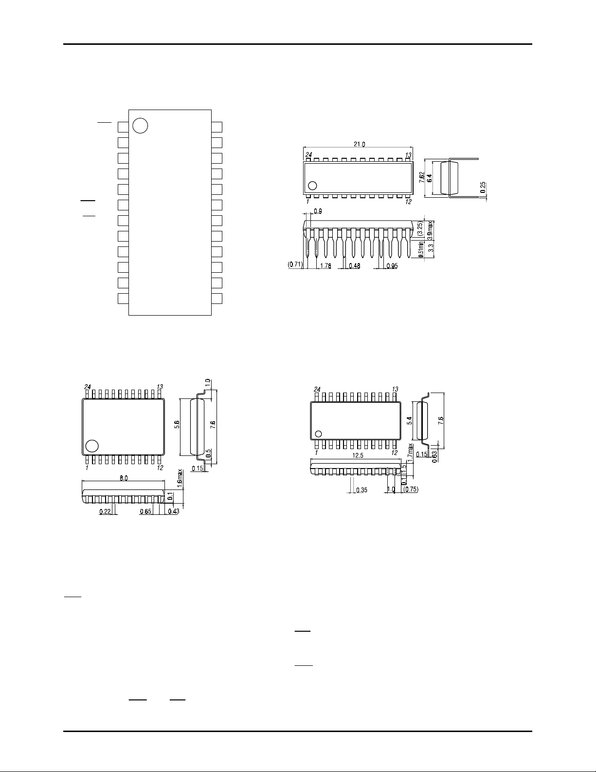
Package Dimensi on
(unit : mm)
3067A
SANYO : DIP24S(300mil)
Package Dimension
(unit : mm)
3175A
Package Dimensi on
(unit : mm)
3112A
SANYO : SSOP24(275mil) SANYO : MFP24S(300mil)
Pin Functions
OSC1, OSC2 : Ceramic Oscillator fo r OSC, RC TEST : Test
: Reset AD0-AD7 : AD converter analog input
RES
PA0-3 : Common I/O port A0-3 SQR : Square wave output
PC0-3 : Common I/O port C0-3 WDR : Watch Dog Reset pin
PD0-3 : Common I/O port D0-3
PE0-1 : Common I/O port E0-1 SI : Serial Input pin
PF0-3 : Common I/O port F0-3 SO : Serial Output pin
Notes: • SQR and WDR are common with PE0 and PE1 respectively.
SI, SO,
•
SCK
, and
are common with PF0 to PF3 respectively.
INT
: Interrupt Request pin
INT
: Serial Clock input/output pin
SCK
No.6727-4/21
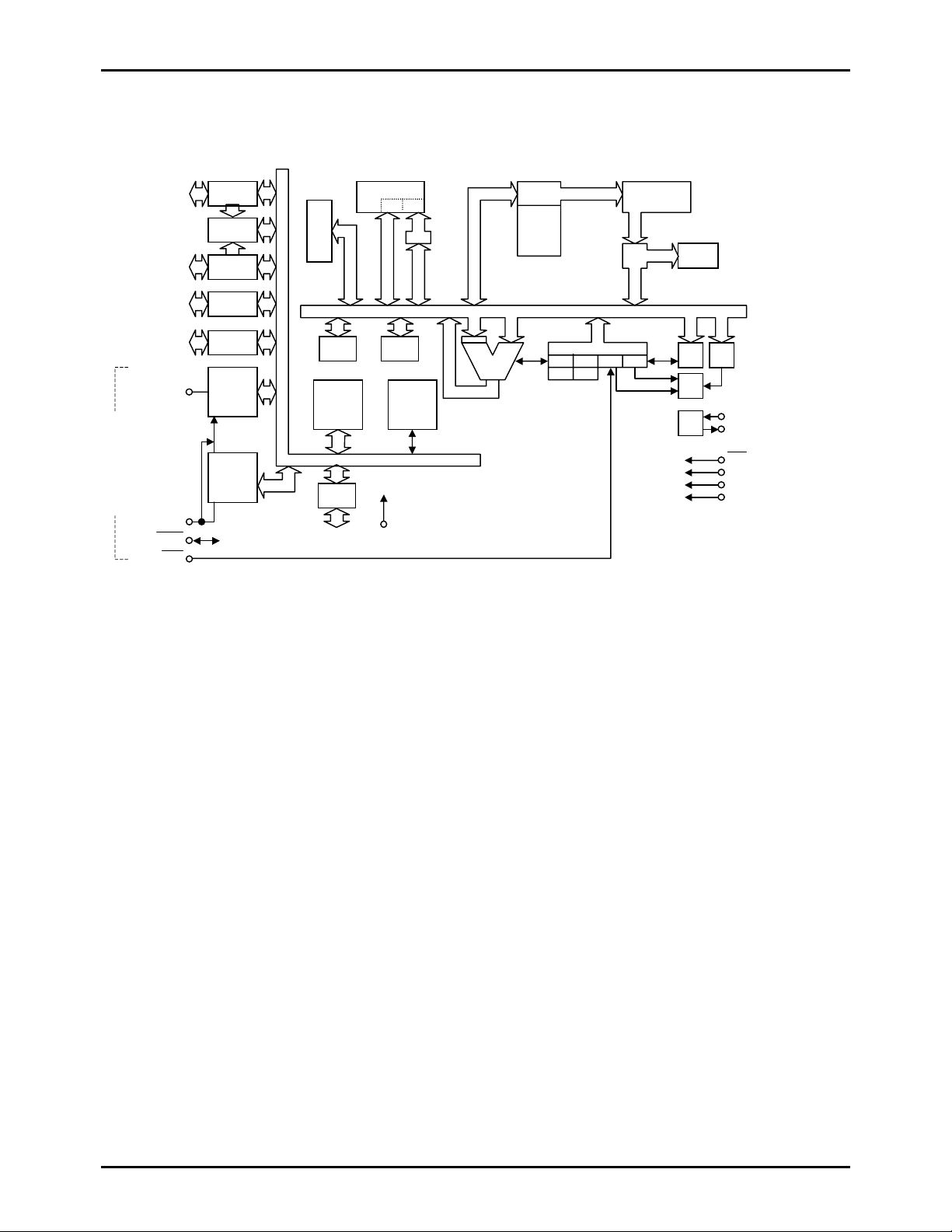
LC651306A/04A/02A/01A
g
g
PA0-3
System Block Diagram
LC651306A/1304A/1302A/1301A
Shared with port F
PF2/SCK
PF3/INT
AD0-3
PF0-3
AD4-7
PC0-3
PD0-3
PF1/SO
4/8 bit
4 bit
PF0/SI
Port A
8-BIT
ADC
Port F
Port C
Port D
Serial
shift
register
lower di
Serial
shift
register
hi
4/8 bit
her digit
I/O Buffer
Serial
mode
register
it
Port E
PE0-1
RAM
F WR
E AC
Serial
mode
register
I/O Bus
WDR
DP
System Bus
ALU
PC
STACK
to
STACK
CF
CSF
STS
ZF
EXTF
RAM : Data Memory ROM : Program Memory
F : Flag PC : Program Counter
WR : Working Register INT : Interrupt control
AC : Accumulator IR : Instruction Register
ALU : Arithmetic and Logic Unit I.DEC : Instruction Decoder
DP : Data Pointer CF, CSF : Carry Flag, Carry Save Flag
E : E register ZF, ZSF : Zer o Flag, Zero Sav e Flag
CTL : Control register EXTF : External Interrupt Request Flag
OSC : Oscillation Circuit TMF : Internal Interrupt Request Flag
TM : Timer
STS : Status register
IR
TMF
ROM
I.DEC
TM CTL
INT
OSC
OSC1
OSC2
RES
TEST
VDD
VSS
No.6727-5/21
LC651306A/04A/02A/01A
P
o
P
Development Support
The following are currently in the development stage and will soon be available to the user for the development of the
LC651306A/04A/02A/01A.
1. User’s manual
Refer to the “LC65F1306A/LC651300 series user’s manual.”
2. Development tool manual
Refer to the “EVA86000 Development Tool Manual for 4-bit microcontrollers.”
3. Software manual
“LC65/66 Series Software Manual”
4. Development tool
a. For program development (EVA86000 system)
b. For program evaluation
Microcontroller with Flash ROM (LC65F1306)
Pin Functions
Symbol
VDD 1 - Power supply - - VSS 1 -
OSC1 1 Input
OSC2 1 Output
PA0-PA3/
AD0-AD3
PC0-PC3 4 I/O •I/O port C0 to C3
PD0-PD3 4 I/O •I/O port D0 to D3
Number
of pins
4 I/O • I/O port A0 to A3
I/O Function Option At reset
Pins for connecting system clock
•
oscillation RC or ceramic resonator.
Leave OSC2 open when OSC1 is used
•
for an external clock input
Input in 4-bit unit (IP instruction)
Output in 4-bit unit
(OP instruction)
Testing in 1-bit unit
(BP, BNP instructions)
Set and reset in 1-bit unit
(SPB, RPB instructions)
PA3 is used for standby mode control.
•
Chattering should not be occurred on
•
the PA3 during HALT instruction
execution.
All four pins have shared function.
•
PA0/AD0:AD converter input AD0
PA1/AD1:AD converter input AD1
PA2/AD2:AD converter input AD2
PA3/AD3: converter input AD3
The port functions are identical to those
of PA0 to PA3 (See note).
The output during a reset can be
•
selected to be either high or low as an
option.
Note: This port has no standby mode
The port functions and options are
identical to those of PC0 to PC3.
control function.
(1) Two-pin RC oscillator,
external clock
(2) Two-pin ceramic oscillator
(3) Divider option
1. No divider
2. Divide by 3
3. Divide by 4
(1) Open-drain output
(2) Pull-up resistor
(1), (2) can be specified in bit
unit.
(1) Open-drain output
(2) Pull-up resistor
(3) High level output during reset.
(4) Low level output during reset.
(1) and (2) can be specified in
•
bit unit.
(3) and (4) are specified 4 bits
•
at a time
Same as PC0 to PC3. Same as PC0 t
- -
High-level
output (The
output
N-channel
transistor s in
the off state.)
High-level
•
output.
Low-level
•
output.
(Depending on
options
selected)
PC3.
Handling
when unused
Select the
open-drain
output option
and connect to
VSS.
Same as PA0 to
A3.
Same as PA0 to
A3.
No.6727-6/21
/WDR
SCK
INT
Number
of pins
2 I/O
4 I/O
1 Input
I/O Function Option At reset
I/O port E0 to E1
•
Input in 4-bit unit (IP instruction)
Output in 4-bit unit (OP instruction)
Set and reset in 1-bit unit
(SPB and PRB instructions)
Testing in 1-bit unit
(BP and BNP instructions)
PE0 also has a continuous pulse (64 Tcyc)
•
output function.
PE1 becomes the watchdog reset pin WDR
•
when selected as an option.
I/O port F0 to F3
•
The port functions and options are identical
to those of PE0 to PE1 (See note).
PF0 to PF3 have shared functions with the
•
serial interface pins and the
The function can be selected under program
control.
SI... Serial input pin
SO...Serial output pin
SCK
INT
The serial I/O function can be switched
between 4-bit and 8-bit transfers under
program control.
Note: There is no continuous pulse output
function.
All four pins have shared function.
•
PF0/AD4: AD converter input AD4
PF1/AD5: AD converter input AD5
PF2/AD6: AD converter input AD6
PF3/AD7: AD converter input AD7
System reset input
•
Provide an external capacitor for the
•
power-on reset.
Apply low level to this pin for 4 or more
•
clock cycles to reset and restart the program.
Test pin for LSI.
•
This pin must be connected to VSS during
normal operation.
Symbol
PE0-PE1
PF0/SI/AD4
PF1/SO/AD5
PF2/
/AD6
PF3/
/AD7
RES
TEST 1 Input
LC651306A/04A/02A/01A
input.
INT
...Input and output of the serial clock
signal.
...Interrupt request signal
Handling
when
unused
(1) Open -drain output
(2) Pull-up resistor
Options (1) or (2) can be
•
specified in bit unit.
(3) Normal port PE1
(4) Watchdog reset WDR
Either options (3) or (4)
•
can be selected.
Identical to those for PA0 to
PA3.
- - -
- - This pin
High level
output (The
output
N-channel
transistor s in
the off state)
Identical to those
for PA0 to PA3.
The serial port
functions are
disabled.
The interrupt
source is set to
.
INT
Identical to
those for
PA0 to PA3.
Identical to
those for
PA0 to PA3.
must be
connected to
VSS.
No.6727-7/21
 Loading...