SANYO LA17000M Datasheet
Ordering number: ENN6522
SANYO Electric Co.,Ltd. Semiconductor Company
TOKYO OFFICE Tokyo Bldg., 1-10, 1 Chome, Ueno, Taito-ku, TOKYO, 110-8534 JAPAN
Monolithic Linear IC
LA17000M
Tuner System IC with Built-in PLL
for Car Audio Applications
Overview
The LA17000M is an all-in-one car tuner IC that incorporates a PLL frequency synthesizer and all functions of an
AM/FM tuner in a single chip. By combining two chips, a
PLL (LC72144 equivalent) and an FM tuner IC (LA1781M
equivalent) into a single chip (*PLL + AM (up conversion)
+ FMFE + IF + NC + MCP + MRC), and as a result of
optimal chip partitioning, the LA17000M improves the
performance of car tuner systems, eliminates adjustments,
and provides high reliability, all at a lower cost.
Features
• PLL on chip
• ADC (6 bits, 1 channel)
• IF counter and I/O port on chip permit simplification
of the interface.
• Supports AM double conversion.
• Enhanced noise countermeasures
• Excellent tri-signal characteristics
• Improved medium and weak electric field NC
characteristics
• Improved separation characteristics
• Anti-birdie filter on chip (analog/digital output)
• Multipath sensor output (analog/digital output)
• Cost-saving features
• AM double conversion (Up conversion method)
• Enhanced FM-IF circuit
(When there is interference from adjacent frequencies,
the software handles switching of the CF between
wide and narrow automatically.)
• Because deviations in IF gain are only 1/3 that of
earlier devices, adjustment is simplified when this IC
is incorporated into a set; this IC also includes a shifter
pin for VSM adjustment.
• Suited for smaller devices
• Permits high-frequency signal line processing in a
tuner pack.
• Easily conformes to FCC standards
Package Dimensions
unit: mm
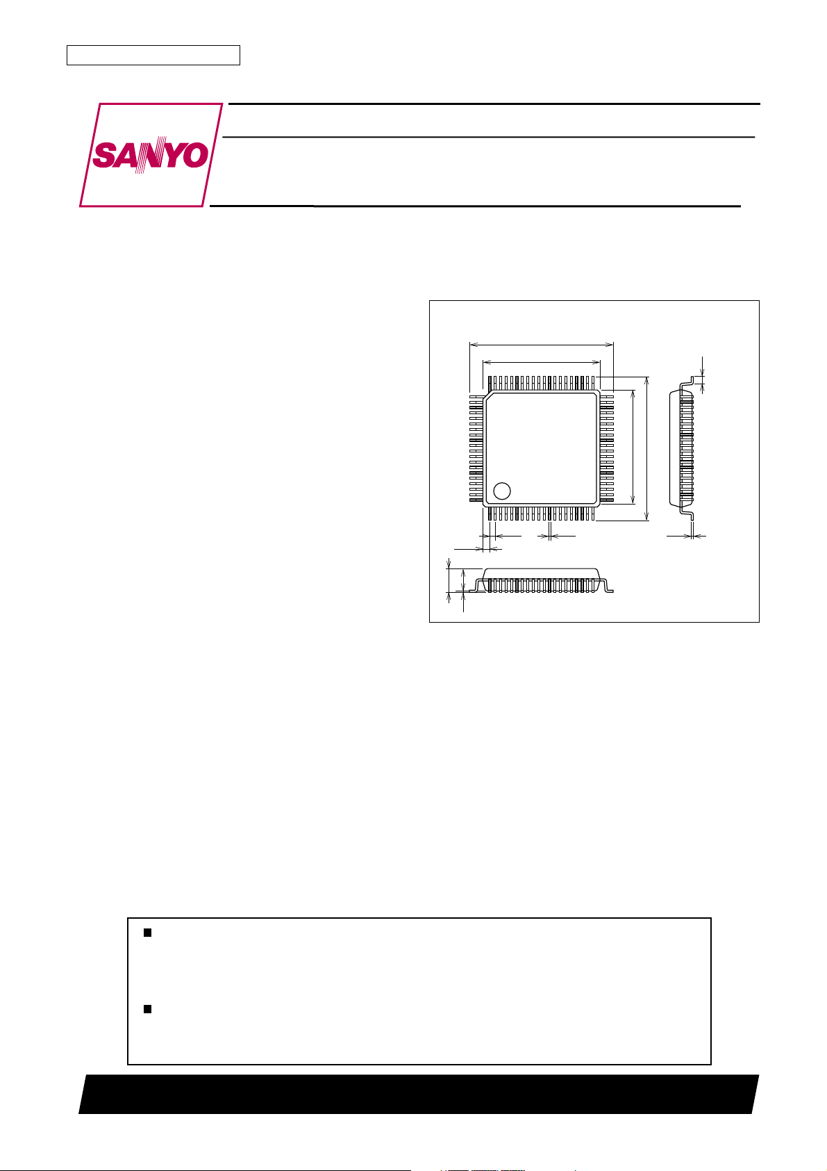
3255-QFP80
[LA17000M]
17.2
61
80
(0.83)
(2.7)
3.0max
0.1
14.0
1
0.65
0.25
4160
40
21
20
0.8
14.0
17.2
0.15
SANYO: QFP80 (14 x 14)
Any and all SANYO products described or contained herein do not have specifications that can handle
applications that require extremely high levels of reliability, such as life-support systems, aircraft’s
control systems, or other applications whose failure can be reasonably expected to result in serious
physical and/or material damage. Consult with your SANYO representative nearest you before using
any SANYO products described or contained herein in such applications.
SANYO assumes no responsibility for equipment failures that result from using products at values that
exceed, even momentarily, rated values (such as maximum ratings, operating condition ranges, or other
parameters) listed in products specifications of any and all SANYO products described or contained
herein.
62901RM (II) No. 6522-1/54
LA17000M
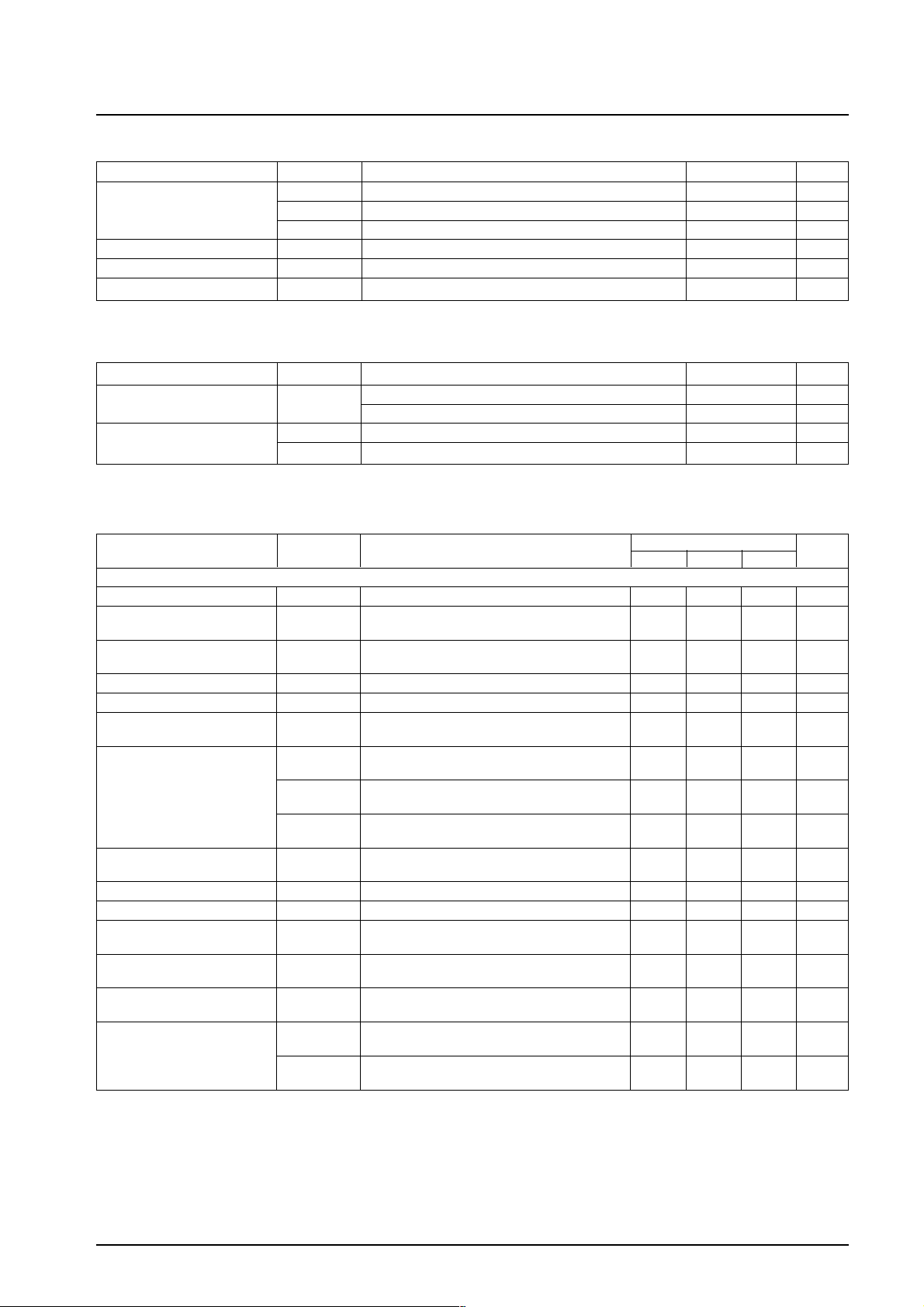
Maximum Ratings at Ta = 25°C
Parameter Symbol Conditions Ratings Unit
VCC1 max Pins 6, 56, and 77 8.7 V
Maximum supply voltage
Allowable power dissipation Pd max Ta ≤ 85°C, * With board 950 mW
Operating temperature Topr –40 to +85 °C
Storage temperature Tstg –40 to 150 °C
VCC2 max Pins 7, 61, 70, 75, and 76 12.0 V
VDD max Pin 19 6.0 V
* Specified board: 114.3 × 76.1 × 1.6 mm3, glass epoxy
Operating Conditions at Ta = 25°C
Parameter Symbol Conditions Ratings Unit
Recommended supply voltage V
Operating supply voltage range
VCC op 7.5 to 8.5 V
VDD op 4.5 to 5.5 V
CC
Pins 6, 7, 56, 61, 70, 75, 76, and 77 8.0 V
Pin 19 5.0 V
Tuner Block
Operating Characteristics at Ta = 25°C, VCC = 8.0 V, VDD = 5.0 V, in the specified Test Circuit
Parameter Symbol Conditions
[FM characteristics] FM IF input
Current drain I
Demodulated output 220 330 445 mVrms
Channel balance CB –1 0 +1 dB
Total harmonic distortion THD-FMmono 10.7 MHz, 100 dBµV, 1 kHz, 100% mod, pin 15 0.4 1 %
Signal-to-noise ratio IF S/N-FM IF 10.7 MHz, 100 dBµV, 1 kHz, 100% mod, pin 15 75 82 dB
AM suppression ratio IF AMR IF 55 68 dB
Muting attenuation Att-1 3 8 13 dB
Separation Separation 25 35 dB
Stereo ON level ST-ON Pilot modulation at which V17 < 0.5 V 4.1 6.6 %
Stereo OFF level ST-OFF Pilot modulation at which V17 > 3.5 V 1.2 3.1 %
Main total harmonic distortion THD-Main L 0.4 1.2 %
Pilot cancellation PCAN 12 22 dB
SNC output attenuation AttSNC 1 5 9 dB
HCC output attenuation AttHCC-1 1 5 9 dB
-FM No input, I56 + I61 + I70 + I75 + I76 + I79 60 98 110 mA
CCO
Att-2 13 18 23 dB
Att-3 26 31 36 dB
AttHCC-2 6 10 14 dB
10.7 MHz, 100 dBµV, 1 kHz, 100%mod,
pin 15 output
10.7 MHz, 100 dBµV, 1 kHz,
ratio of pin15 and pin 16
10.7 MHz, 100 dBµ, 1 kHz, fm = 1 kHz, pin 15
at 30% AM
10.7 MHz, 100 dBµV, 1 kHz, attenuation on
pin 15 when V49 = 0 → 2 V
10.7 MHz, 100 dBµV, 1 kHz, attenuation on
pin 15 when V49 = 0 → 2 V *Note 1
10.7 MHz, 100 dB µV, 1 kHz, attenuation on
pin 15 when V49 = 0 → 2 V *Note 2
10.7 MHz, 100 dBµ, L + R = 90%,
pilot = 10%, pin 15 output ratio
10.7 MHz, 100 dBµV, L + R = 90%,
pilot = 10%, pin 15
10.7 MHz, 100 dBµV, pilot = 10%,
pin 15 signal/PILOT-LEVEL leak DIN AUDIO
10.7 MHz, 100 dBµV, L – R = 90%,
pilot = 10%, V44 = 3 V → 0.6 V, pin 15
10.7 MHz, 100 dBµV, 10 kHz, L + R = 90%,
pilot = 10%, V45 = 3 V → 0.6 V, pin 15
10.7 MHz, 100 dBµV, 10 kHz, L + R = 90%,
pilot = 10%, V45 = 3 V → 0.1 V, pin 15
Ratings
min typ max
Unit
Continued on next page.
No. 6522-2/54
LA17000M
Continued from preceding page.
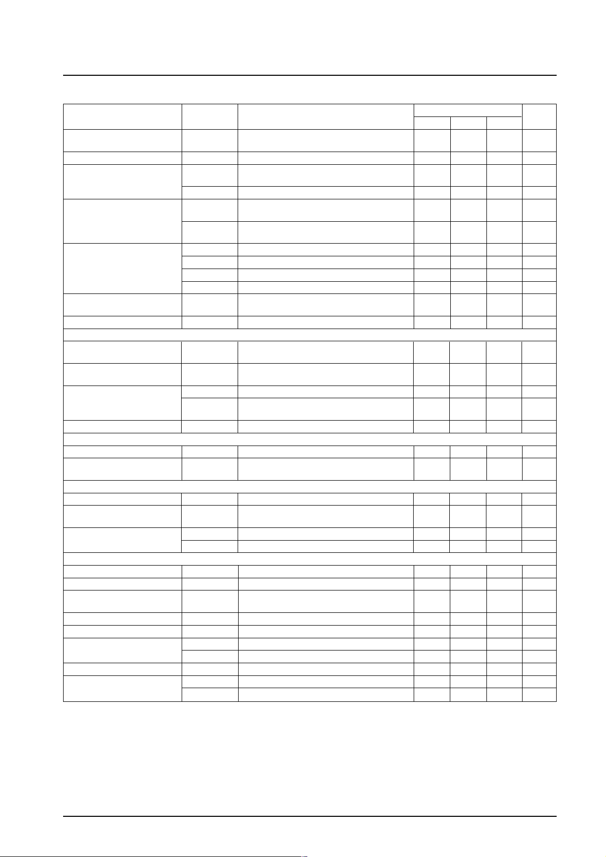
Parameter Symbol Conditions
Input limiting voltage VIN-LIM 29 36 dBµV
10.7 MHz, 100 dBµV, 30% mod, IF input that
decreases the input reference output by –3 dB
Muting sensitivity VIN-MUTE IF input level non-mod when V49 = 2 V 19 27 35 dBµV
SD sensitivity SD-sen1 FM 48 56 64 dBµV
IF input non-mod (at least 100 mVrms) at
which the IF count buffer output turns on
SD-sen2 FM 48 56 64 dBµV
IF counter buffer output V
Signal meter output V
IFBUFF-FM
V
IFBUFF-FM
FM-1 No input, pin 42 DC output non-mod 0.0 0.1 0.3 V
SM
V
FM-2 50 dBµ, pin 42 DC output non-mod 0.65 1.6 2.4 V
SM
V
FM-3 70 dBµ, pin 42 DC output non-mod 2.4 3.2 4.2 V
SM
V
FM-4 100 dBµ, pin 42 DC output non-mod 4.9 5.8 6.5 V
SM
Muting bandwidth BW-MUTE 140 210 280 kHz
10.7 MHz, 100 dBµV, non-mod, pin 38 output,
1 145 245 330 mVrms
during SEEK
10.7 MHz, 100 dB µV, non-mod,
2 145 245 330 mVrms
pin 38 output, during RDS mode
100 dBµV, when V49 = 2 V
Bandwidth non-mod
Muting drive output V
-100 100 dBµV, 0 dBµ, pin 49 DC output non-mod 0.00 0.1 0.3 V
MUTE
[FM FE Block]
N-AGC on input V
W-AGC on input V
NAGC
WAGC
83 MHz, non-mod, input at which pin 2 is
2.0 V or less
83 MHz, non-mod, input at which pin 2 is
2.0 V or less (when KEYED-AGC is 4.0 V)
Conversion gain A. V1 83 MHz, 80 dBµ, non-mod, FECF output 9 13 17 dB
A. V2 13 17 21 dB
83 MHz, 80 dBµ, non-mod, 5 V applied to CF
(pin 10), FECF output
Oscillator buffer output V
OSCBUFFFM
No input, pin 5 output 51 67 102 mVrms
[NC Block] NC input (pin 30)
Gate time
Noise sensitivity SN 18 mVp-o
τ
GATE f = 1 kHz, 1 µs, 100 mVp-o pulse input 15 µs
1 kHz, 1 µs pulse input that starts noise
canceller operation. Measured at Pin 30.
[MRC Block]
MRC output V
MRC
MRC operating level MRC-ON 22 33 44 mVrms
V42 = 5 V 2.1 2.25 2.4 V
Input level on pin 48 that is below
pin 42 = 5 V and pin 43 = 2 V, f = 70 kHz
MRC sensor output V
-sensor1 V42 = 5 V, pin 34 output 1.5 1.9 V
MRC
V
MRC-
sensor2
V42 = 5 V, pin 48 output, f = 70 kHz, 100 mVrms
[AM Characteristics] AM ANT input
Practical sensitivity S/N-30 1 MHz, 30 dBµV, fm = 1 kHz, 30% mod, pin 15 15 dB
Detection output VO-AM 1 MHz, 74 dBµV, fm = 1 kHz, 30% mod, pin 15 105 160 220 mVrms
AGC-F.O.M V
AGC-FOM
1 MHz, 74 dBµV, output reference, input width
at which output drops by 10 dB, pin 15
Signal-to-noise ratio S/N-AM 1 MHz, 74 dBµV, fm = 1 kHz, 30% mod 47 52 dB
Total harmonic distortion THD-AM 1 MHz, 74 dBµV, fm = 1 kHz, 80% mod 0.5 1.2 %
Signal meter output VSMAM-1 1 MHz, 30 dBµV, non - mod 0.6 1 1.4 V
VSMAM-2 1 MHz, 120 dBµV, non - mod 3.4 4.5 5.9 V
Oscillator buffer output
V
OSCBUFF
AM-1
No input, pin 5 output 170 210 mVrms
Wideband AGC sensitivity W-AGCsen1 1.4 MHz, input when V62 = 0.7 V 87 93 99 dBµV
W-AGCsen2
1.4 MHz, input when V62 = 0.7 V (during SEEK)
Ratings
min typ max
72 79 86 dBµV
90 97 104 dBµV
2.1 2.9 V
50 55 60 mVrms
78 84 90 dBµV
Unit
Continued on next page.
No. 6522-3/54
LA17000M
Continued from preceding page.
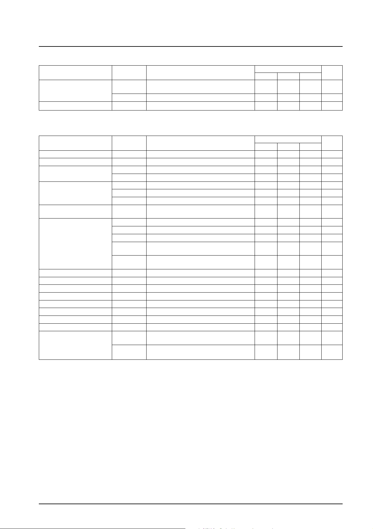
Parameter Symbol Conditions
SD sensitivity SD-sen1AM 27 33 39 dBµV
SD-sen2AM 1 MHz,
IF buffer output V
IFBUFF-AM
1 MHz, ANT input level at which IF count
output turns on
ANT
input level at which SD pin turns on
1 MHz, 74 dBµV, non-mod, pin 38 output 150 220 mVrms
Ratings
min typ max
27 33 39 dBµV
Unit
PLL Block
Allowable Operating Ranges at Ta = –40 to +85°C, VDD = 5 V, VSS = 0 V
Parameter Symbol Conditions
High-level input voltage VIH1 CE, CL, DI, I/O-1, I/O-2 2.2
Low-level Input voltage VIL1 CE, CL, DI, I/O-1, I/O-2, SDSTSW 0 0.8 V
Output voltage VO1 DO 0 6.5 V
VO2 I/O-1, I/O-2 0 13 V
Input amplitude fIN1XIN; Sine wave, capacitor coupled 1 8 MHz
fIN2 PLLIN; Sine wave, capacitor coupled 10 160 MHz
fIN3 HCTR; Sine wave, capacitor coupled 0.4 25 MHz
Guaranteed crystal oscillator
ranges
Input amplitude VIN1X
Data setup time t
Data hold time t
Clock low-level time t
Clock high-level time t
CE wait time t
CE setup time t
CE hold time t
Data latch change time t
Data output time t
X’tal 10.1 10.5 MHz
VIN2-1 PLLIN; 10 ≤ f < 130 MHz; Note 2 40 1500 mVrms
VIN2-2 PLLIN; 130 ≤ f <160 MHz; Note 2 70 1500 mVrms
VIN3-1 40 1500 mVrms
VIN3-2 70 1500 mVrms
SU
HD
CL
CH
EL
ES
EH
LC
DC
t
DH
XIN, X
(X’tal: 10.25, 10.35 MHz); Note 1
IN
HCTR; 0.4 ≤ f < 25 MHz: Serial data;
CTC = 0: Note 3
HCTR; 8 ≤ f <12MHz: Serial data;
CTC = 1: Note 4
DI, CL: Note 5 0.45 µs
DI, CL: Note 5 0.45 µs
CL: Note 5 0.45 µs
CL: Note 5 0.45 µs
CE, CL: Note 5 0.45 µs
CE, CL: Note 5 0.45 µs
CE, CL: Note 5 0.45 µs
Note 5 0.45 µs
DO, CL; Dependent on pull-up resistance,
board capacity: Note 5
DO, CL; Dependent on pull-up resistance,
board capacity: Note 5
; CI ≤ 70 Ω
OUT
Ratings
min typ max
VDD + 0.3
200 1500 mVrms
Unit
0.2 µs
0.2 µs
V
Note 1: Recommended CI value for crystal oscillator
CI ≤ 70 Ω (X’tal: 10.25, 10.35 MHz)
However, because the characteristics of the X’tal oscillation circuit depend on the board and circuit constants,
we recommend requesting that the X’tal manufacturer perform the evaluation.
Note 2: Refer to the program divider configuration.
Note 3: Serial data: CTC = 0
Note 4: Serial data: CTC = 1
Note 5: Refer to the serial data timing.
No. 6522-4/54
LA17000M
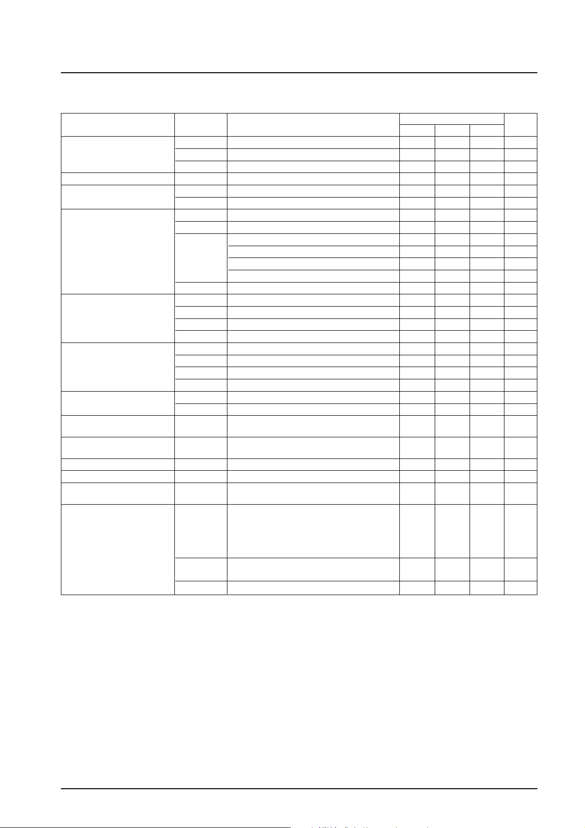
PLL Characteristics
Electrical Characteristics at Ta = 25°C, VDD = 5 V, VSS = 0 V
Parameter Symbol Conditions
Built-in feedback resistors Rf1 X
Rf2 PLL
IN
IN
Rf3 HCTR 250 kΩ
Hysterisis width V
HIS
CE, CL, DI 0.1V
High-level output voltage VOH1 PD1, PDS, SEEKSW; IO = –1 mA VDD–1.0 V
VOH2 XBUF; IO = –0.5 mA VDD–1.5 V
Low-level output voltage VOL1 PD1, PDS, SEEKSW; IO = –1 mA 1 V
VOL2 XBUFF; IO = –0.5 mA 1.5 V
VOL3 I/O-1 to I/O-2; IO = 1.0 mA 0.2 V
I/O-1 to I/O-2; IO = 2.5 mA 0.5 V
I/O-1 to I/O-2; IO = 5.0 mA 1 V
I/O-1 to I/O-2; IO = 9.0 mA 1.8 V
VOL4 DO; IO = 5.0 mA 1 V
High-level input current IIH1 CE, CL, DI; VIN = 6.5 V 5 µA
IIH2 I/O-1 to I/O-2; VIN = 13 V 5 µA
IIH3XIN; VIN = V
IIH4 PLLIN; VIN = V
DD
DD
Low-level input current IIL1 CE, CL, DI; VIN = 0 V 5 µA
IIL2 I/O-1 to I/O-2; VIN = 0 V 5 µA
IIL3X
; VIN = 0 V 2 11 µA
IN
IIL4 PLLIN; VIN = 0 V 4 22 µA
Output off leakage current I
High-level 3-state off leakage
1 I/O-1 to I/O-2; VO = 13 V 5 µA
OFF
I
2 DO; VO = 6.5 V 5 µA
OFF
I
OFFH
PD1, PDS; VIN = V
DD
current
Low-level 3-state off leakage
I
OFFL
PD1, PDS; VIN = 0 V 0.01 200 nA
current
Input capacitance C
IN
A/D converter linearity error Err MRC SENSOR AUTO ADJ (MOS) –0.5 +0.5 LSB
Pull-down transistor on
resistance
Supply current IDD11015mA
Rpd1 PLL
VDD; X’tal = 10.25 MHz,
IN
fIN2 = 160 MHz,
VIN2 = 70 mVrms,
fIN3 = 25 MHz,
VIN3 = 40 mVrms
Ratings
min typ max
1MΩ
500 kΩ
DD
211µA
422µA
0.01 200 nA
6pF
80 200 600 kΩ
Unit
V
IDD2510mA
VDD; PLL block halt (PLL INHIBIT),
X’tal OSC operation (10.25 MHz)
IDD3VDD ; PLL block halt, X’tal OSC halt 3 mA
No. 6522-5/54
FM RF AGC
FE GND
FMOSC
OSC BUFFER
AM/FM
AM OSC
NC Sens
NC AGC
XBUFF IN
Gore OUT
LPF OUT
MPX Pdot IN
NC MPX GND
Lch OUT
Rch out
SDSTSW
PLL IN
PLL V
DD
FM MIX IN
FM ANTD
1 2 3 4 5
0.022
µ
F
16V/100
µ
F
0.022µF
0.022
µ
F
0.022
µ
F
8pF
k
k
10.7Hz
10.7MHz
450kHz
1000pF
100
µ
H
FC18
2.2
µ
H
16V/47
µ
F
0.022
µ
F
0.022
µ
F
16V/47
µ
F
0.01
µ
F0.01
µ
F
0.01
µ
F
0.022
µ
F
82pF 82pF
68pF
0.022
µ
F
0.022
µ
F
3.3
µ
F
0.1
µ
F
100
µ
H
0.022
µ
F
33mH
100µH
65pF
6pF
15pF
1SV234
1SV234
0.022
µ
F
30
3
7
4
6
2
k
Ω
6 7 8 9 10 11 12 13 14 15 16 17 18 19
AM/FM S-METER
42
MRC OUT
43
SNC
44
HCC
45
NC IN
46
DET OUT
47
FM S-METER MRC IN
48
MUTE
49
AFC IN
50
QD OUT
51
QD IN
52
V
REF
53
FM SD
54
KEYED AGC
55
V
CC
56
C-HCC
57
AM LC
58
PILOT DET
59
IF AGC
60 41
PD1
20
PLL V
SS
21
PDS
22
XBUFF
23
I/O2
24
X IN
25
X OUT
26
CE
27
CI
28
CL
29
DO
30
I/O1
31
HCTR
32
SEEKSW
33
MRC SENSOR OUT ADC 0
34
PC IN
35
PC OUT
36
MPX VCO
37
IF COUNT BUFF SEEK/STOP SELECT
38
GND
39
40
80
AM 1st MIX IN
79
1st IF IN (NARROW)
78
FE V
CC
77
MIX OUT
76
MIX OUT
75
NARROW AGC IN/MUTE ATT ADJ
74
AM RF AGC OUT
73
1st IF (WIDE)
72
AM SD ADJ/WIDE AGC IN
71
AM MIX OUT
70
1st IF OUT
69
AM IF IN
68
FM IF IN
67
FM IF BYPASS
66
2nd MIX IN
65
RF AGC
64
FM MUTE ADJ
63
AM ANTD/WIDE AGC
AM FT
62
61
LA17000M
+
+
+
+
+
+
+
+5V
—5V
—
+
0.022
µ
F
0.01µF
CC
270pF
30pF
100pF
1M
Ω
NC
U
30k
Ω
0.47
µ
F
0.015
µ
F
100pF
0.01
µ
F
0.1
µ
F
0.01
µ
F
1000pF
1µF
1
234
987
6 712-12
1025MHz
0.01µF
1
µ
F
180pF
112NME
112LDA
0.1
µ
F
1
µ
F
1
µ
F1
µ
F
0.047
µ
F
1
µ
F
0.22
µ
F
0.022µF
912kHz
16V/10
µ
F
16V/1
µ
F
16V/100µF
16V/1
µ
F
0.022
µ
F
0.01
µ
F
0.22
µ
F
0.22
µ
F
22
µ
F
1
µ
F
3.3
µ
F
0.022
µ
F
10.7Hz
10.7Hz
51k
Ω
10k
Ω
50
Ω
51k
Ω
350
Ω
CR
50
Ω
10k
Ω
10k
Ω
SOFP80
10k
Ω
2SK583
1M
Ω
50
Ω
10k
Ω
47k
Ω
200
Ω
22pF
22pF
47k
Ω
47k
Ω
33k
Ω
5.6k
Ω
PHASE COMP
50
Ω
1k
Ω
330
Ω
47k
Ω
15k
Ω
1M
Ω
100k
Ω
P1
100k
Ω
10k
Ω
100k
Ω
100k
Ω
43k
Ω
10k
Ω
30k
Ω
20k
Ω
10k
Ω
10k
Ω
SIGNAL
-
MATER
-
Z
SEP
-
VOL
-
L
SEP
-
VOL
-
H
SW11
NC
-
IN
-
GND
NC
-
IN
DET
-
OUT
MRC
-
IN
MUTE
SW12
DET
-
ADJ
SYS-PS+15V
SYS-PS-GND
SYS-PS-—15V
DZ1
SYS-PS+12V
CENTER-MATER
AM-STREO-OUT
AM-STREO-OUT-GND
1st-IF-OUT
SW13
SW14
FM-IF-INPUT
SW40
SW41
RF-MIX-V
CC
RF-MIX-V
CC
-
G
AM-V
CC
AM-ANT-INPUT
AM-ANT-DUMP
FM-ANT-INPUT
SW01
FM-ANT-DUMP
FM-AGC
FM-MIX-INPUT
10k
Ω
6.8k
Ω
10k
Ω
100
k
Ω
10k
Ω
240k
Ω
L78MO5T
IGO
82pF
82pF
8200pF
750pF
82pF
SVC203
VR
P1
2.2k
Ω
D
G
S
150pF
6800pF
112LDA
112LDA
1M
Ω
30pF
P1
0.015
µ
F
P1
+
16V/100
µ
F
0.01µF
FM
-
V
CC
SW18
OSC
-
BUFF
-
OUT
NC
-
HPF
-
OUT
SW02
CF SW
SW03
SW04
SW05
GATE
-
OUT
L
-
CH
-
OUT
NC
-
LPF
-
OUT
R
-
CH
-
OUT
ST
-
SD
SW06
VF/IMZ
-
G
VF/IMZ
-
S
VF/IMZ
-
F
PLL -V
CC
VT-OUT
2nd-OSC-BUFF
IOZ
SW17
X-IN
DUT-CCB-CE
DUT-CCB-CL
DUT-CCB-DI
DO
IO1
SW16
IF-COUNT-IN
IF-COUNT-BUFF
MRC-SENSOR-OUT
SW07
MPX-FREO
SIGNAL-MATER-1
MRC-OUT
SW08
SW09
VDDSNC/HCC1
5V
FMIF AM NC MPX V
CC
PLL
-
IN
CC
3
U
7
4
6
2
+
+5V
—5V
—
0.01µF
CC
0.01µF
CC
CR
+12V
NC
3
7
6
5
1
2
+
+15V
—
NC
NC
0.1
µ
F
3
7
5
1
4
6
2
+
+15V
—15V
—15V
—
0.1µF
0.01
µ
F
NC
NC
0.1µF
3
7
8
1
4
5
6
2
+
—15V
+15V
+15V
+15V
+5V
—5V
—15V
+12V
—
0.1µF
NC
NC
0.1µF
3
7
5
1
4
6
2
+
—15V
—15V
—
0.1µF
NC
NC
0.1µF
0.01
µ
F
50
Ω
1M
Ω
+5V
3
7
4
6
2
+
—5V
—
0.01µF
0.01µF
0.022
µ
F
0.022
µ
F
50
Ω
330
Ω
4
0.1µF
PLL V
CC
D
C
B
S
E
G
0.022µF
1M
Ω
50
Ω
3
U
7
4
6
2
+
+5V
—5V
—
0.01µF
CC
0.01µF
CC
CR
50
Ω
50
Ω
1M
Ω
CR
50
Ω
3
U
7
4
6
2
+
+5V
—5V
—
0.01µF
CC
0.01µF
CC
CR
5pF
10pF
18pF
100pF
30
Ω
150
Ω
30
Ω
200k
Ω
30k
Ω
510
Ω
100
Ω
30k
Ω
200k
Ω
3SK263
30k
Ω
150
Ω
560
Ω
33
Ω
100k
Ω
100k
Ω
0.01
µ
F
2200pF
180pF
180k
Ω
100k
Ω
50
Ω
25
Ω
30
Ω
10pF
15pF
18k
Ω
1SV234
1SV234
1000pF
16V/100
µ
F
+
15pF
1000pF
50
Ω
16V/47
µ
F
0.01
µ
F
+
L79MO5T
IGO
A13289
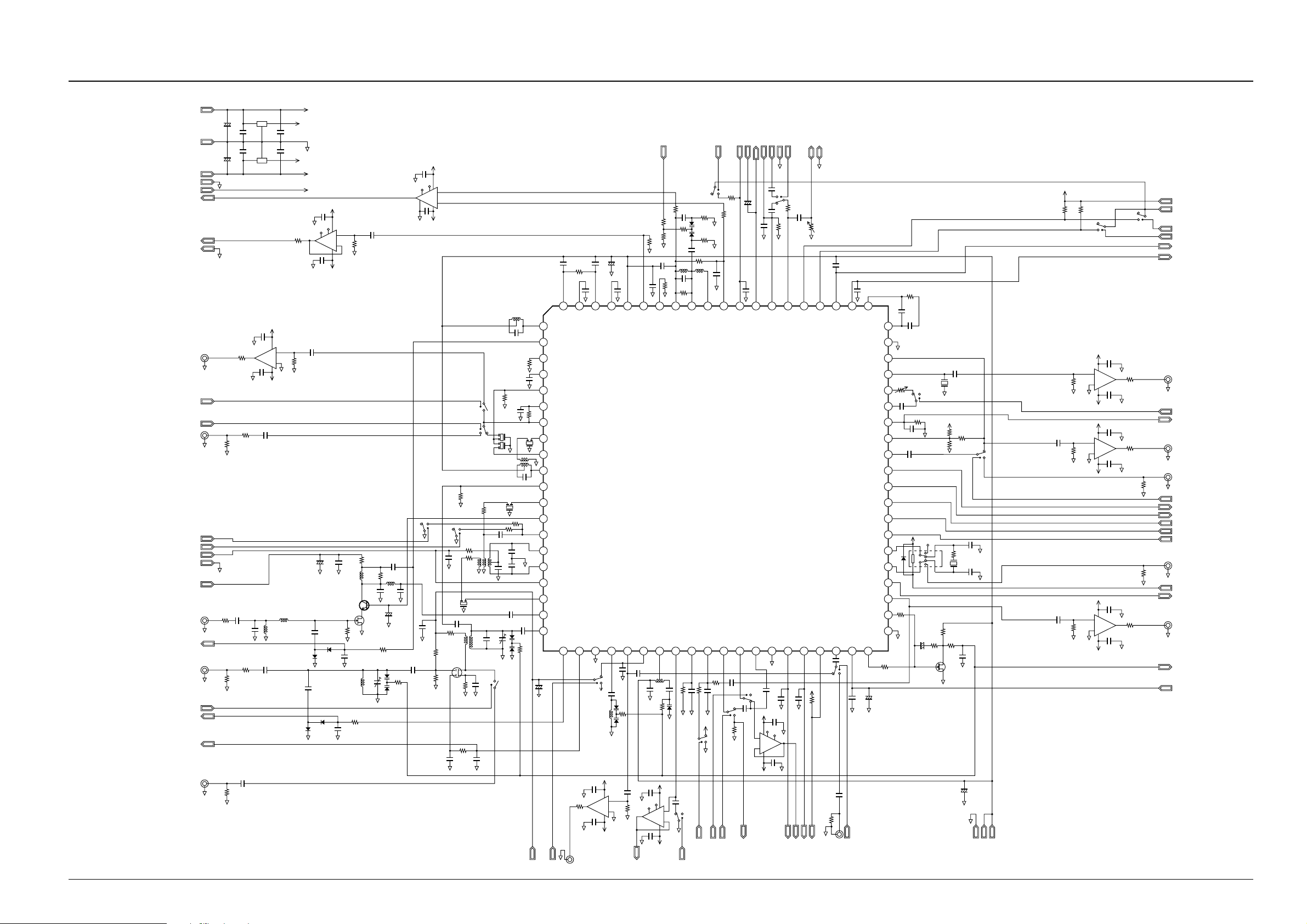
Test Circuit
LA17000M
No. 6522-6/54

LA17000M
[FM IF Selectivity Switching Circuit]
Features
1) Comprises an FM/AM one-chip system.
2) Up conversion method is adopted for AM.
3) Uses an IF filter with a center frequency that is the same as the middle frequency of FM.
4) Uses a narrowband filter in AM mode.
5) Uses a narrowband filter in FM mode only during SEEK or when there is interference from adjacent frequencies.
6) Uses a wideband filter for normal reception in FM mode.
7) For an RDS AF search, switches to a narrowband filter and detects SD.
8) High sensitivity for detecting interference from adjacent frequencies.
Advantages
1) This FM/AM one-chip tuner system (an IC that includes a microcontroller interface) allows for improved adjacent
frequency interference characteristics without increased cost.
2) Prevents SD and IF count misdetection (station detection) during seek search, RDS AF search, and auto memory
operations.
3) Permits adoption of an IC for certain functions without increasing the number of IC pins.
4) CF selectivity can be switched by the software in the microcontroller that controls the tuner, making it easy to
achieve performance differentiation through the software.
(The software can freely set the CF switching timing and conditions.)
5) Detects the radio wave status in the field through detection of SD, desired station field intensity, IF count output, and
adjacent station field intensity. This IC offers improved adjacent frequency interference characteristics by switching
the CF automatically when interference is being generated from an adjacent frequency.
[IF Band Switching Circuit]
Purpose
This AM/FM one-chip tuner IC automatically switches the FM selectivity, prevents misdetection during SEEK operations, and offers improved adjacent frequency interference characteristics without any increase in cost.
New Technological Features
1. Comprises an AM/FM one-chip IC.
2. Because the narrowband CF that is used by the AM UP conversion system is also used for FM, additional external
components required by earlier systems can be eliminated.
3. Uses a wideband CF during normal FM reception for high sound quality.
4. Uses a narrowband CF for AM reception, and if interference is being generated from adjacent frequencies during
FM reception.
5. Uses a narrowband CF during SEEK and RDSAF search operations, preventing misdetection of SD and IF count
due to adjacent stations.
6. CF switching is performed at the first IF amp input, and the amp gain is adjusted automatically to a suitable level
according to the CF band form AM/FM or FM.
7. Switching of the CF input and the first IF amp gain is controlled by a microcontroller through the interface. The
pins that are controlled are connected to the I/O ports of the microcontroller, and are controlled by the
microcontroller’s internal software.
8. Detection of adjacent frequency interference during FM reception is based on S-meter output, SD, and IF count
output. The IF count buffer frequency fluctuates when interference is being generated from adjacent frequencies.
This fluctuation is used to make the detection of interference from adjacent frequencies possible. (Related patents
have been applied for.)
Conventional Technologies
1. Comprised of a dedicated IC for IF band switching, or of multiple ICs.
2. None of the AM/FM all-in-one chip systems include the functions provided by the LA17000M.
3. Requires a narrowband CF especially for FM, resulting in increased costs. (Does not share the AM narrowband CF.)
4. Because CF switching control is handled by analog circuits or logic circuits, the switching timing can only be
controlled through uniform conditions. Control by software is not possible.
No. 6522-7/54
LA17000M
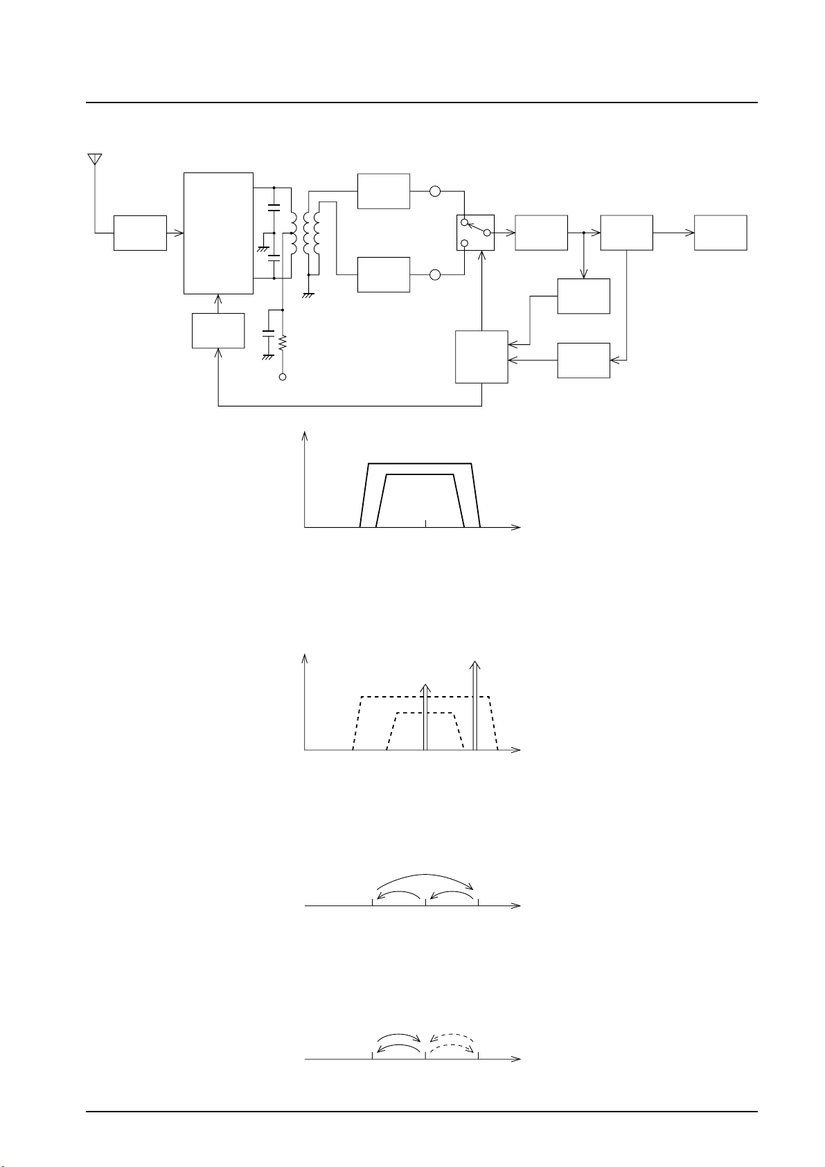
Conceptual Diagram of the FM-IF Band Switching System
Wideband
filter
FM
RF
Mixing
Local
oscillation
Wideband
filter
Limiter
amp
FM
DET
Narrowband
filter
SL
Control
circuit
V
CC
LO
Level
IF
counter
Field
intensity
A13290
Wideband
A
Narrowband
10.7
f (MHz)
A13291
Fud
Fd
B
10.7
C
D
FdFdL FdH
FdFdL FdH
f (MHz)
A13292
A13293
A13294
No. 6522-8/54
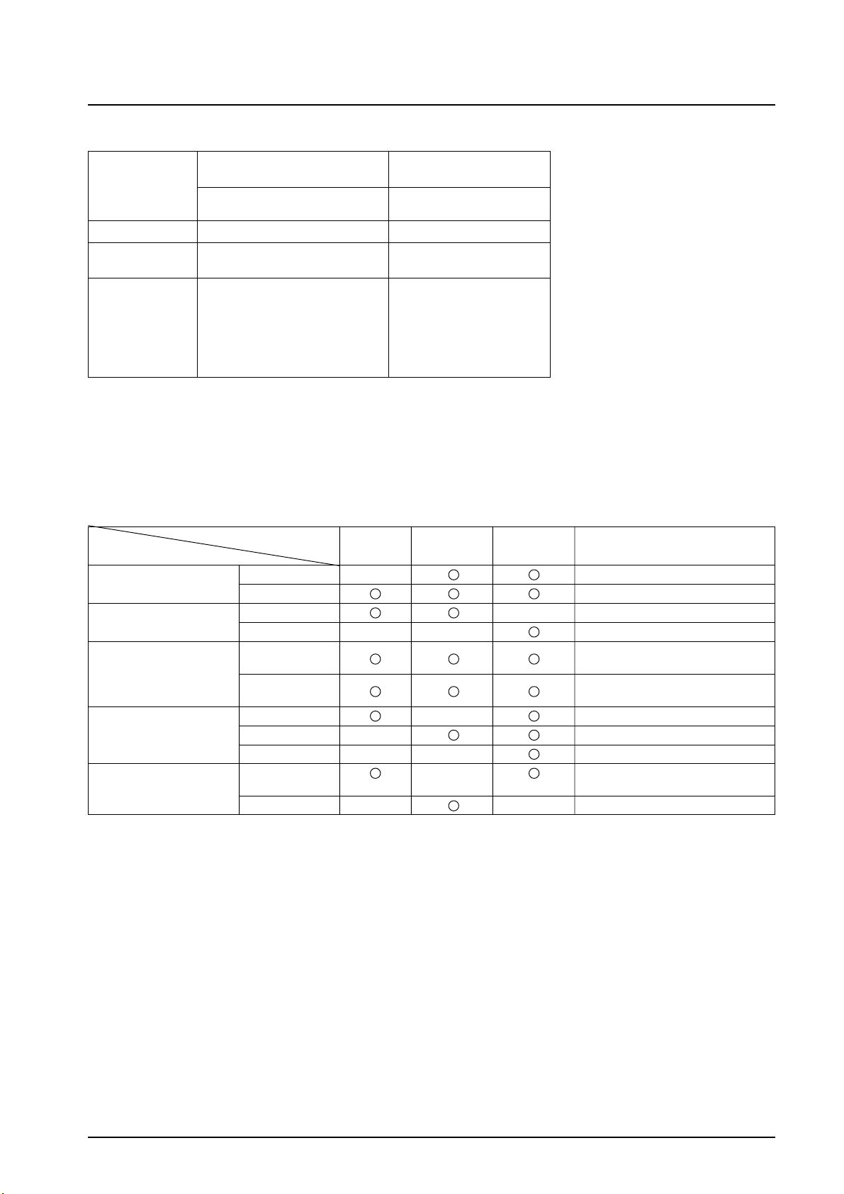
I/O Port Assignment Table
LA17000M
I/O-0
DI data
I/O-1
I/O-2
DI data
I/O-3
DO data
OUTPUT
PLL output port
INPUT
PLL input port
OUTPUT
PLL output port
INPUT
I/O-3 = 0 (input port)
OUT3 = 1 (OPEN or high)
PLL input port
Cannot be set as output port
L: Reception mode
H: Seek mode
OPEN: RDS
Unused
H: Dx mode
L: Lo mode
When reception mode is set
H: Monaural
L: Stereo
When seek mode is set
H: SD ON
L: SD OFF
The MRC sensor reads DO data from the PLL microcontroller’s 6-bit A/D converter.
Currently, aside from the CCB data lines, only three lines are connected to the controller microcontroller: CF/SW,
AUDIO mute, and AM/FM band switching port.
Selectivity Switching Evaluation Software State-based Data Switching Table
Tuner processing
I/O port state
CF switching
AUDIO mute output
Lo/Dx
Mode switching
IF count
WIDE
NARROW
ON Switchable but fixed by software
OFF Switchable but fixed by software
Lo
Dx
Seek mode I/O-3 is SD output
Reception mode I/O-3 is monaural/stereo output
RDS mode I/O-3 is SD output
Output ON Seek mode
Output OFF Reception mode
Seek Manual preset Receiving Remarks
Processing is performed according
to the setting
Processing is performed according
to the setting
RDS mode
No. 6522-9/54

LA17000M
Additional Settings (Added to the LC72144M)
Output (DI)
Mode Settings When set
DI data IN2
Seek mode For seek
Tuner mode switch Reception mode For seek-stop and for receiving
RDS mode For AF search
Lo mode When setting Lo mode
Lo/Dx switch
Dx mode When setting Dx mode
Mute ON For tuning processing
Hard mute *1
Mute OFF When switching reception mode
I/O-0 = 1 (output port)
OUT0 = 1 (Hi)
DI data IN2
I/O-0 = 1 (output port)
OUT0 = 0 (Lo)
DI data IN2
I/O-0 = 0 (input port)
OUT0 = 1 (OPEN)
DI data IN2
I/O-2 = 0 (output port)
OUT2 = 0 (Lo)
DI data IN2
I/O-2 = 1 (output port)
OUT2 = 1 (Hi)
DI data IN2
I/O-0 = 1 (output port)
OUT1 = 1 (Hi)
DI data IN2
I/O-0 = 1 (output port)
OUT1 = 1 (Lo)
Note: *1. Depends on the I/O ports usage.
Input (DO)
DO data Conditions
When the tuner mode is set to
reception mode
*2
When the tuner mode is set to seek or
RDS mode
*2
Start AD conversion and then read
after conversion is completed.
3.3 V at 6-bit resolution
Sensor
MRC output
Monaural/stereo
SD
OUT data I3 = 1 (Hi)
Monaural state
OUT data I3 = 0 (Lo)
Stereo state
OUT data I3 = 1 (Hi)
SD ON
OUT data I3 = 0 (Lo)
SD OFF
OUT data ADC0
AD00 to AD05
6 bit
Note: *2. I/O-3 = 0 (input port) and OUT3 = 1 (Hi) must already be set in the DI data (IN2) settings.
Other settings
In the LA17000 Setting When set
Hi: Wide (wideband setting)
CF switch Pin 10 When there is interference from
Soft mute (AUDIO mute) Pin 49
AM/FM switch Pin 6
Lo: Narrow (narrowband
setting)
Hi: Forced mute When setting mute
Lo: Mute off When cancelling mute
Lo: AM For AM reception
Hi: FM For FM reception
For normal operation
adjacent frequencies
No. 6522-10/54
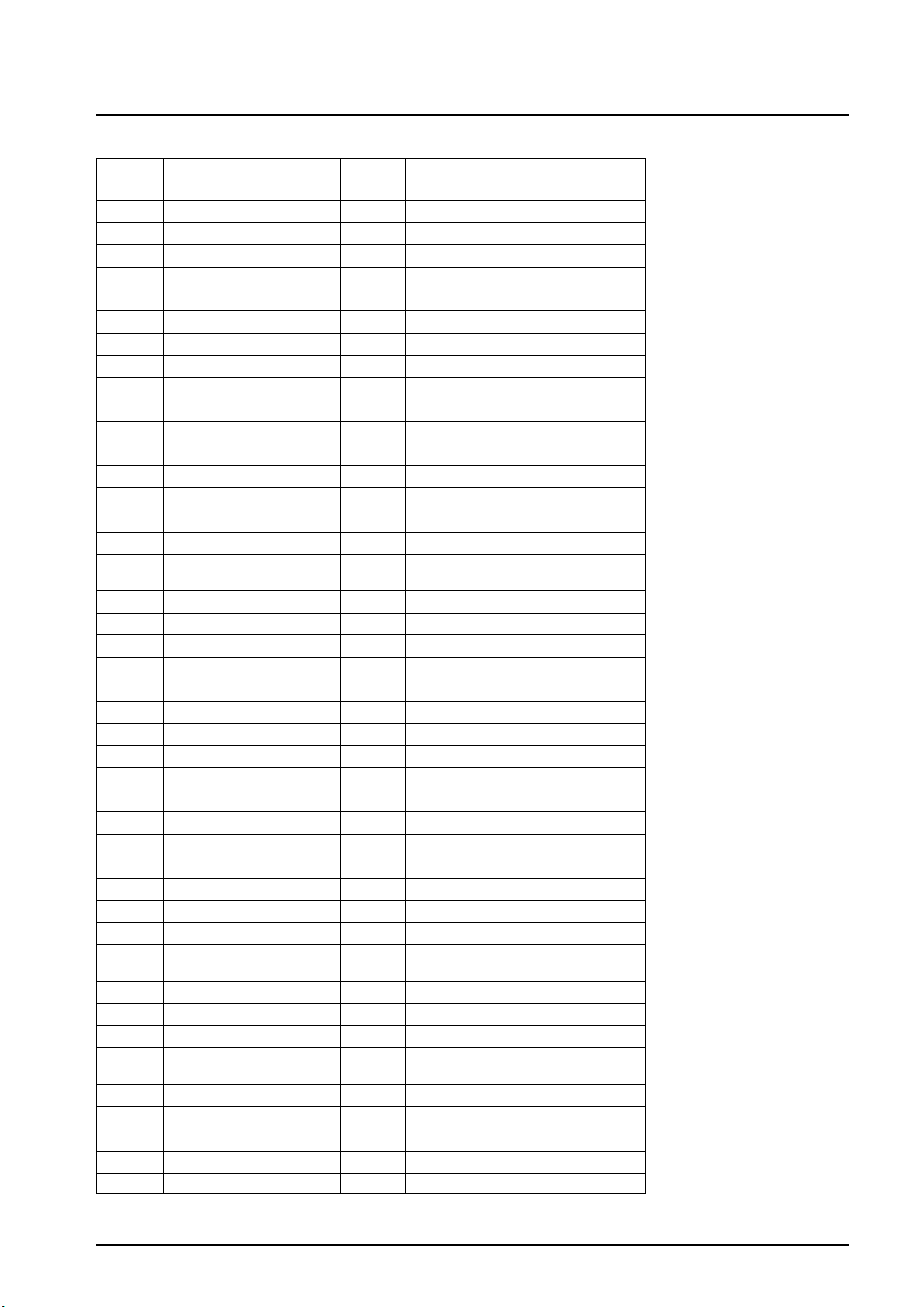
LA17000M
Correspondence of Pins Between the LA17000M, the LA1781M, and the LC72144M
LA1781
Pin No. Pin No. Pin No.
Pin Function
LA17000M
Pin Function
LC72144M
1 FN ANTD 1
2 FM RF AGC 2
3 FE GND 3
4 FM OSC 4
5 AM/FM OSC buff. 5
6 FE V
7 AM V
CC
CC
6
7
8 Noise AGC-Sense 8
9 Noise AGC-ADJ 9
10 AM 2nd OSC 10
11 Gate Out 11
12 Memory circuit pin 12
13 Pilot In 13
14 NC, MPX GND 14
15 MPX L-Out 15
16 MPX R-Out 16
26 Seek → AM/FM SD 17 Both I/O-3 and SD/ST-IND 23
Stop → FM ST IND
18 FMIN 16
19 V
DD
17
20 PD1 18
21 V
SS
19
22 PDS 20
23 XBUF 22
24 I/O-2 8
25 XIN 24
26 XOUT 1
27 CE 2
28 DI 3
29 CL 4
30 DO 5
31 I/O-1 9
32 HCTR/I-6 11
33 I/O-0 12
19 MRC sensor output 34 7
Both ADC0 and MRC
sensor output
17 Pilot Can. ADJ 35
18 Pilot Can. ADJ 36
20 MPX VCO 37
23 38
IF count buffer and
seek/stop switch
25 GND 39
21 PHASE COMP. 40
22 PHASE COMP. 41
24 AM/FM S-meter 42
27 MRC OUT 43
Continued on next page.
No. 6522-11/54
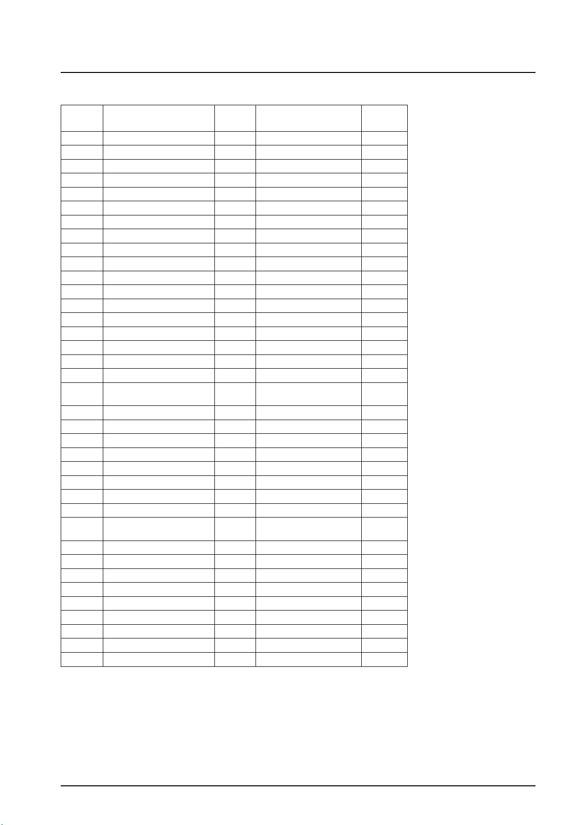
Continued from preceding page.
LA17000M
LA1781
Pin No. Pin No. Pin No.
28 SNC control input 44
29 HCC control input 45
30 Noise canceller IN 46
31 AM/FM detector output 47
32 FM S-meter output 48
33 MUTE drive 49
34 AFC IN 50
35 QD OUT 51
36 CD IN 52
37 VREF 53
38 FMSD 54
39 GND Keyed AGC 55
40 V
41 HCC capacitor 57
42 AM L.C. 58
43 Pilot detector 59
44 IF AGC 60
45 AM IFT (IF output) 61
46 AM ANTD 62
47 FM Mute ON ADJ 63
48 RF AGC 64
49 AM 2nd MIX IN 65
50 FM IF BYPASS 66
51 FM IF IN 67
52 AM IF IN 68
53 1st IF amplifier output 69
54 AM MIX OUT 70
55 W-AGC IN 71
56 1st IF IN 72
57 AM RF AGC OUT 73
58 N-AGC IN 74
59 1st MIX OUT 75
60 1st MIX OUT 76
61 F.E.V
64 FM MIX IN 78 1st IF narrow IN
62 AM MIX IN 79
63 FM MIX IN 80
Pin Function
CC
W-AGC IN
AM SD ADJ
CC
LA17000M
56
77
Pin Function
LC72144M
No. 6522-12/54

LA17000M
PLL Block Functions
• High-speed programmable divider
• FMIN : 10 to 160 MHz .......................... Pulse swallower method
• General-purpose counter
• HCTR : 0.4 to 25.0 MHz ........................ Frequency measurement
• Crystal oscillator : Two frequencies selectable: 10.35/10.25 MHz
• Reference frequencies : 12 frequencies selectable:
50, 30, 25, 12.5, 6.25, 3.125, 10, 9, 3, 5, and 1kHz
*1 *1 *1
*1: Not available when using the 10.25 MHz crystal oscillator
• Phase comparator
• Dead zone can be controlled
• Unlock detection circuit
• Sub-charge pump for high-speed locking
• Deadlock clear circuit on chip
• A/D converter ................................6 bits: 1 input (linked directly to MRC sensor output)
• Serial data I/O
Communications with controller possible in CCB format
• Power-on reset circuit
• On-chip crystal oscillator output buffer
• 2nd IF injection signal for AM up conversion (10.35/10.25 MHz)
• I/O port ..........................................General-purpose I/O: four ports
No. 6522-13/54
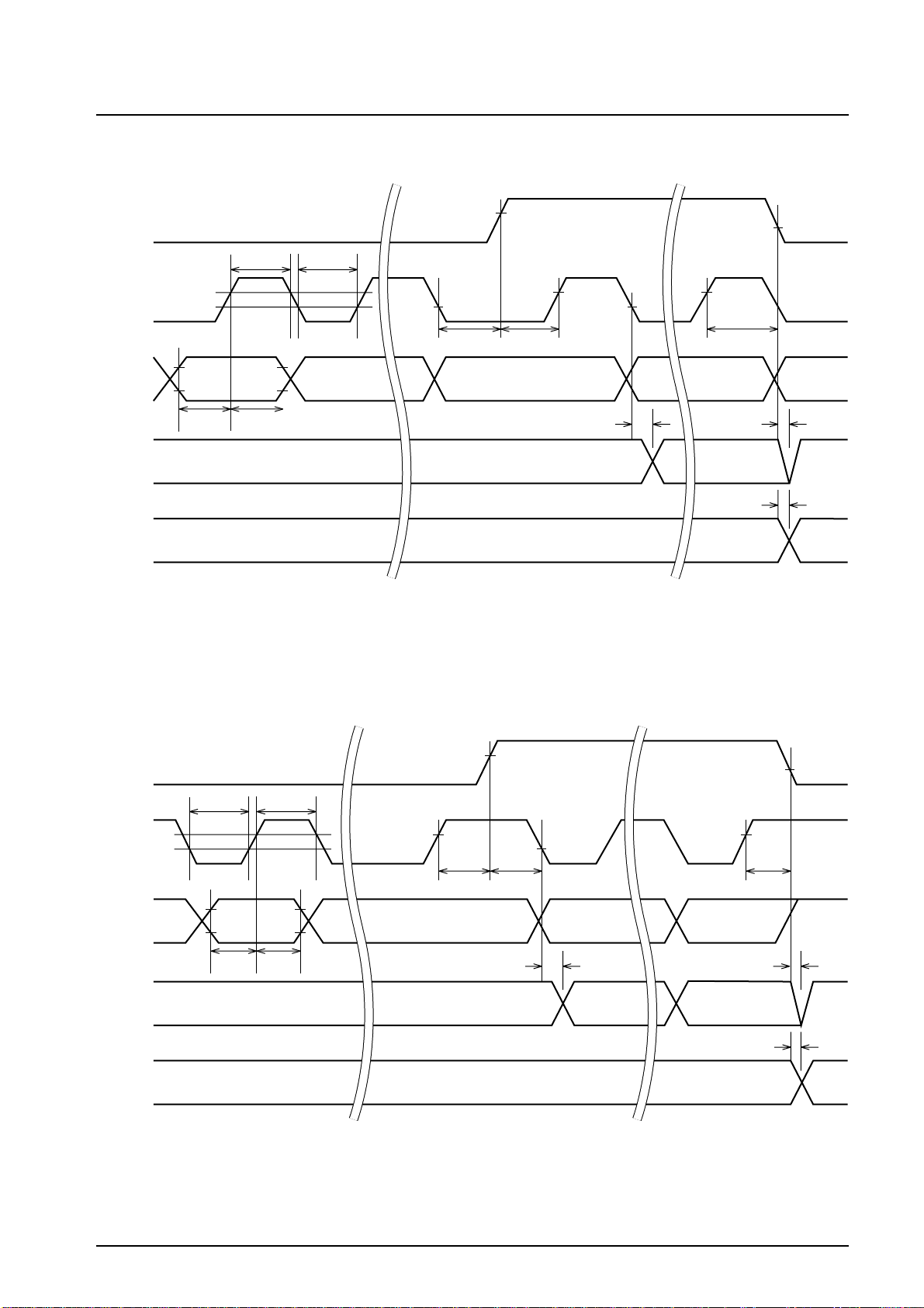
Serial Data Timing
5
6
CE
LA17000M
V
IH
V
IL
CL
DI
DO
Internal
data latch
V
IH
V
IL
V
IH
V
IL
t
SUtHD
t
CH
V
V
IH
IL
t
CL
V
V
IL
t
EL
t
ES
IH
When CL is Stopped at the low level
t
DC
V
V
IL
IH
t
EH
t
DH
t
LC
Old New
A1329
CE
CL
DI
DO
Internal
data latch
V
IH
t
CL
V
IH
V
IL
V
V
IL
t
SUtHD
IH
V
V
t
CH
IH
IL
V
IH
t
EL
t
DC
t
ES
V
IL
V
IH
t
t
t
EH
DH
LC
Old New
V
IL
A1329
When CL is Stopped at the high level
No. 6522-14/54
LA17000M
7
8
2
3
9
0
1
A13304
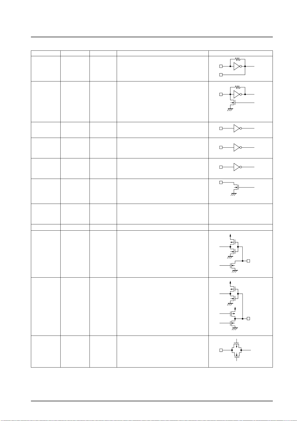
PLL Block Pin Description
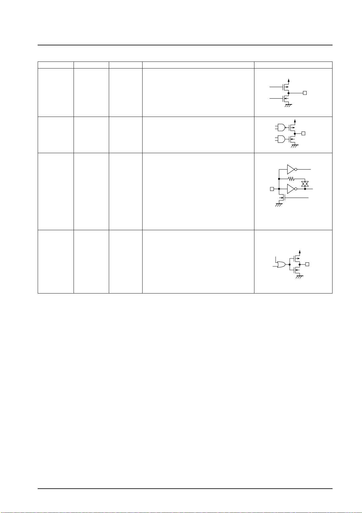
Symbol Pin No. Description Function Pin Circuit
XIN 25 X’tal OSC
XOUT 26
PLL IN 18
Local
oscillator
signal input
CE 27 Chip enable
CL 29 Clock
DI 28 Input data
• For connecting the crystal oscillator.
(10.35, 10.25, 7.2 or 4.5 MHz)
• FMIN is selected when DVS in the serial data
input is set to 1.
• The input frequency range is from 10 to
160 MHz.
• The signal is transmitted to the swallow
counter.
• The divisor can be set to a value in the range
272 to 65535.
• This pin is set high during serial data input to
the PLL (DI) or during serial data output (DO).
• This pin is the clock for data synchronization
during serial data input to the PLL (DI) or
during serial data output (DO).
• This is the input pin for serial data that is
transferred from the controller to the PLL.
A1329
A1329
S
A1329
S
A1330
S
A1330
DO 30 Output data
V
DD
V
SS
I/O-1 31
I/O-2 24
STSD SW 17
SEEK SW 33
19 Power supply
21 Ground • This is the PLL ground pin.
Generalpurpose
I/O ports
Generalpurpose
I/O port
• This is the output pin for serial data that is
transferred from the controller to the PLL.
•
This is the PLL power supply pin. Supply 4.5 V
to 5.5 V to this pin when the PLL is operating.
• When power is first applied to this pin, the
power-on reset circuit operates.
• These are general-purpose I/O ports.
• The output circuits open-drain.
• During a power-on reset, I/O-1 and I/O-2
become input ports. STSD SW becomes an
output port, and is fixed low.
• These ports can be switched between input
and output according to the serial data that is
transferred from the controller (I/O-1, I/O-2,
STSD SW).
• This is a general-purpose I/O port.
• The output circuits are complementary
circuits.
• During a power-on reset, this port becomes
an input port.
• This port can be specified as an input or
output port by the serial data that is transferred from the controller.
A1330
A1330
ADC0 34 ADC input
• This is the A/D converter input pin.
The converter is a 6-bit successive-approximation A/D converter.
For details, refer to the page that describes
the A/D converter configuration.
A13305
Continued on next page.
No. 6522-15/54
LA17000M
9
Continued from preceding page.
Symbol Pin No. Description Function Pin Circuit
PD1 20
0
PDS 22
Main
charge
pump
output
Sub-charge
pump
output
• This is the PLL charge pump output pin.
When the frequency of the local oscillation
signal frequency is divided by N is higher than
the reference frequency, a high level signal is
output from the PD1 pin. When the frequency
is lower, a low level signal is output. If the
frequencies match, the pin goes to high
impedance.
• A high-speed lockup circuit can be formed by
using this pin in combination with the main
charge pump.
• For details, refer to page that describes the
charge pump configuration.
A13306
A13307
HCTR 32
XBUF 23
Generalpurpose
counter
X’tal
oscillator
buffer
• Serial data: HCTR is selected if CTS1 = 1 is
set.
• The input frequency is 0.4 to 25 MHz.
• The signal is passed through to the general-
purpose counter internally, via the 1/2
frequency divider. An integrating count can
also be kept.
• The count result is output from the MSB of
the general-purpose counter through the
output pin DO.
• For details, refer to page that describes the
general-purpose counter configuration.
• Serial data: Prohibited when HCTR = 0.
• This is the output buffer for the crystal
oscillator circuit.
• Serial data: When XB = 1 is set, the output
buffer operates and the crystal oscillator
signal (pulse) is output.
When XB = 0, this pin outputs a low level.
(When a power-on reset is executed, XB = 0
and the output buffer is fixed at the low level.)
A13308
XOUT
A1330
No. 6522-16/54
LA17000M
0
tSU,tHD,tES,tEC,tEH>0.45μs
1
2
Procedures for Input and Output of Serial Data
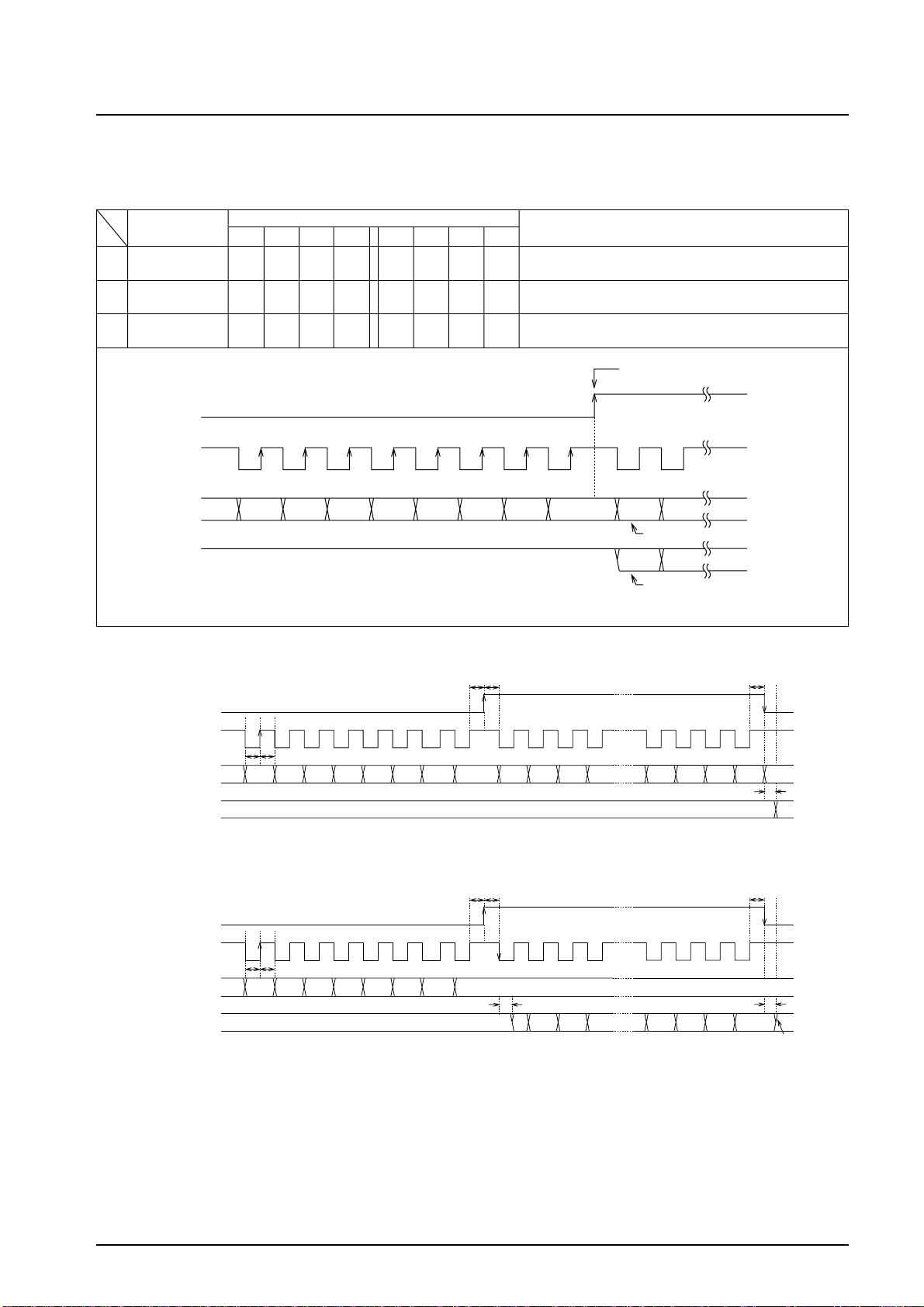
Data I/O is handled through the Computer Control Bus (CCB), SANYO’s audio IC serial bus format. This IC uses CCB
with 8-bit addressing.
I/O mode
B0 B1 B2 B3 A0 A1 A2 A3
Address
[1] IN1 0001 0100
[2] IN2 100 1 0100
[3] OUT 0101 0100
CE
CL
DI
B0 B1 B2 B3 A0 A1 A2 A3
DO
i) Serial Data Input (IN1/IN2)
t
ES
CE
tLC<0.45μs
Description
• Control data input (serial data input) mode.
• 32-bit data input
• Control data input (serial data input) mode.
• 32-bit data input
• Data output (serial data output) mode.
• The bit count output is equal to the clock cycle count.
I/O mode setting
First Data IN1/2
First Data OUT
A1331
t
EC
t
EH
CL
DI
t
SU
t
HD
B0 B1 B2 B3 A0 A1 A2 A3 P0 P1 P2 P3 CTS0 CTS1 GT0 GT1
t
LC
Internal data
A1331
ii) Serial data output (OUT)
tSU,tHD,tES,tEC,tEH>0.45μs
CE
CL
DI
DO
tLC,tDH<0.2μs(*1)
t
SU
t
HD
B0 B1 B2 B3 A0 A1 A2 A3
(*2)
t
ES
*1:Because the DO pin is an N-channel open drain pin, the data transition time varies according to the pull-up resistance
t
EC
t
DC
I7 I6 I5
I4
AD13 AD12 AD11 AD10
t
EH
t
DH
(*2)
A1331
and the board capacitance.
*2:The DO pin is normally open.
No. 6522-17/54
 Loading...