

SANYO LA1650C, LA1650 Datasheet
Ordering number : ENN6310A
30300RM (OT) No. 6310-1/14
Overview
The LA1650 and LA1650C receive long-wave time
standard broadcasts (JG2AS in Japan and DCF77 in
Germany) and detect and output the time code multiplexed
on the long-wave time standard broadcast signal. Clocks
can automatically correct their time using the time code
information received by the LA1650 and LA1650C.
Features
• Low-voltage operation (VCCop = 1.2 V and higher)
• Low current drain (500 µA for @ 10 dBµ V input)
• Standby mode current: Less than 1 µA
• High sensitivity (Reception is possible at
Vin = 10 dBµ V.)
• Packages: DIP18 (LA1650)
Chip (LA1650C)
Functions
• RF amplifier, rectifier, detector, time code output,
standby circuit
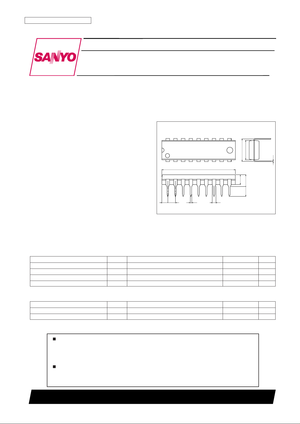
Package Dimensions
unit: mm
3007A-DIP18
1
9
18
10
24.2
1.94 2.54
1.20.5
3.25
3.3
3.85max
0.25
7.62
6.4
SANYO: DIP18
[LA1650]
LA1650, 1650C
SANYO Electric Co.,Ltd. Semiconductor Company
TOKYO OFFICE Tokyo Bldg., 1-10, 1 Chome, Ueno, Taito-ku, TOKYO, 110-8534 JAPAN
Time Code Reception ICs
Monolithic Linear IC
Any and all SANYO products described or contained herein do not have specifications that can handle
applications that require extremely high levels of reliability, such as life-support systems, aircraft’s
control systems, or other applications whose failure can be reasonably expected to result in serious
physical and/or material damage. Consult with your SANYO representative nearest you before using
any SANYO products described or contained herein in such applications.
SANYO assumes no responsibility for equipment failures that result from using products at values that
exceed, even momentarily, rated values (such as maximum ratings, operating condition ranges, or other
parameters) listed in products specifications of any and all SANYO products described or contained
herein.
Parameter Symbol Conditions Ratings Unit
Maximum supply voltage V
CC
max 7.5 V
Allowable power dissipation Pd max Ta ≤ 75°C 100 mW
Operating temperature Topr –20 to +75 °C
Storage temperature Tstg –40 to +125 °C
Specifications
Maximum Ratings at Ta = 25°C
Parameter Symbol Conditions Ratings Unit
Recommended supply voltage V
CC
1.5 V
Operating supply voltage range V
CC
OP 1.2 to 6.5 V
Operating Conditions at Ta = 25°C
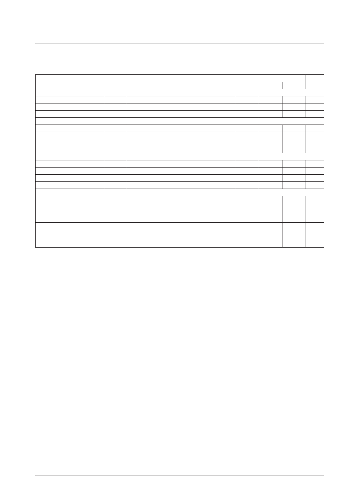
No. 6310-2/14
LA1650, 1650C
Parameter Symbol Conditions
Ratings
Unit
min typ max
[Overall Characteristics]
Current drain I
CCO
No input 400 540 680 µA
Operating current I
CCfIN
= 40 kHz, VIN= 10 dBµV 370 510 650 µA
Standby current ISTB With the pin 5 (pad 5) voltage at 0 V 0.1 1.0 µA
[Amplifier Input Characteristics]
Input impedance ZI 1pin (PAD1) 450 kΩ
Input frequency range FIN 37.5 80.0 kHz
Minimum input voltage V
IN
min Pin 1 (pad 1) input 1 µVrms
Maximum input voltage V
IN
max Pin 1 (pad 1) input 100 mVrms
[Amplifier Output Characteristics] With pin 1 (pad 1) as the input pin, f
IN
= 40 kHz
Output voltage (1) V
O
1 No input, the pin 11 output 10 20 34 mVrms
Output voltage (2) V
O
2VIN= 10 dBµV, the pin 11 output 15 28 48 mVrms
Output voltage (3) V
O
3VIN= 20 dBµV, the pin 11 output 25 40 62 mVrms
Output voltage (4) V
O
4VIN= 80 dBµV, the pin 11 output 35 48 88 mVrms
[TCO Output Characteristics] With pin 1 (pad 1) as the input pin, f
IN
= 40 kHz
Output voltage (high) V
O
H No input 1.40 1.45 V
Output voltage (low) V
O
LVIN= 10 dBµV 0.05 0.10 V
Output pulse width (500 ms input) T500
V
IN
= 0 to 100 dBµV, AM modulation
480 500 650 ms
(1 Hz square wave, duty = 50%, 100% modulation)
Output pulse width (800 ms input) T800
VIN= 0 to 100 dBµV, AM modulation
750 800 970 ms
(1 Hz square wave, duty = 80%, 100% modulation)
Output pulse width (200 ms input) T200
V
IN
= 0 to 100 dBµV, AM modulation
180 200 400 ms
(1 Hz square wave, duty = 20%, 100% modulation)
Operating Characteristics at Ta = 25°C, VCC= 1.5 V, with the pin 5 used as V
CC,
in the specified test circuit,
unless otherwise specified. Values in parentheses refer to the LA1650C. (Using the Yamaichi Electronics IC37N1803 socket.)
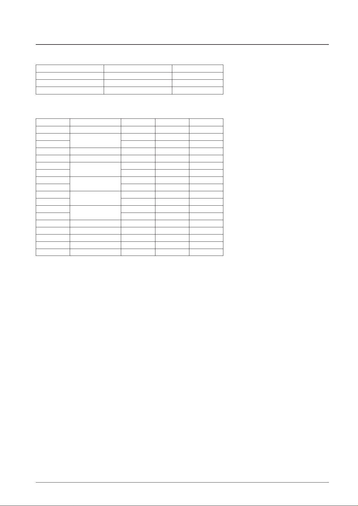
Chip Specifications (LA1650C)
No. 6310-3/14
LA1650, 1650C
Pad Coordinates (LA1650C)
Note: The origin (0, 0) is taken to be the left lower corner in the metal pattern figure on the next page.
The pad coordinates are the values of the coordinates of the center of the pad.
PAD Pad Symbol X-axis Y-axis
P1 Amplifier (1) input INPUT 585 1914
P2
AGC
AGC2 385 1914
P3 AGC1 154 1734
P4 V
CC
V
CC
158 1410
P5 Standby mode PON 154 1221
P6
Amplifier (1) output
AMP1_OUT1 154 711
P7 AMP1_OUT2 164 201
P8
Amplifier (2) input
AMP2_IN1 397 154
P9 AMP2_IN2 597 154
P10
Amplifier (2) output
AMP2_OUT2 864 154
P11 AMP2_OUT1 1086 154
P12
REC input
REC_IN1 1264 361
P13 REC_IN2 1264 531
P14 REC output REC_OUT1 1264 701
P15 DEC input DEC_IN1 1264 1455
P16 DEC output TCO 1264 1625
P17 GND GND 1113 1914
P18 REG REG 849 1914
Chip size 1.41 ×2.06 mm
2
Chip thickness 330 (±20) µm
Pad size 140 × 140 µm
2
Pad opening 115 × 115 µm
2
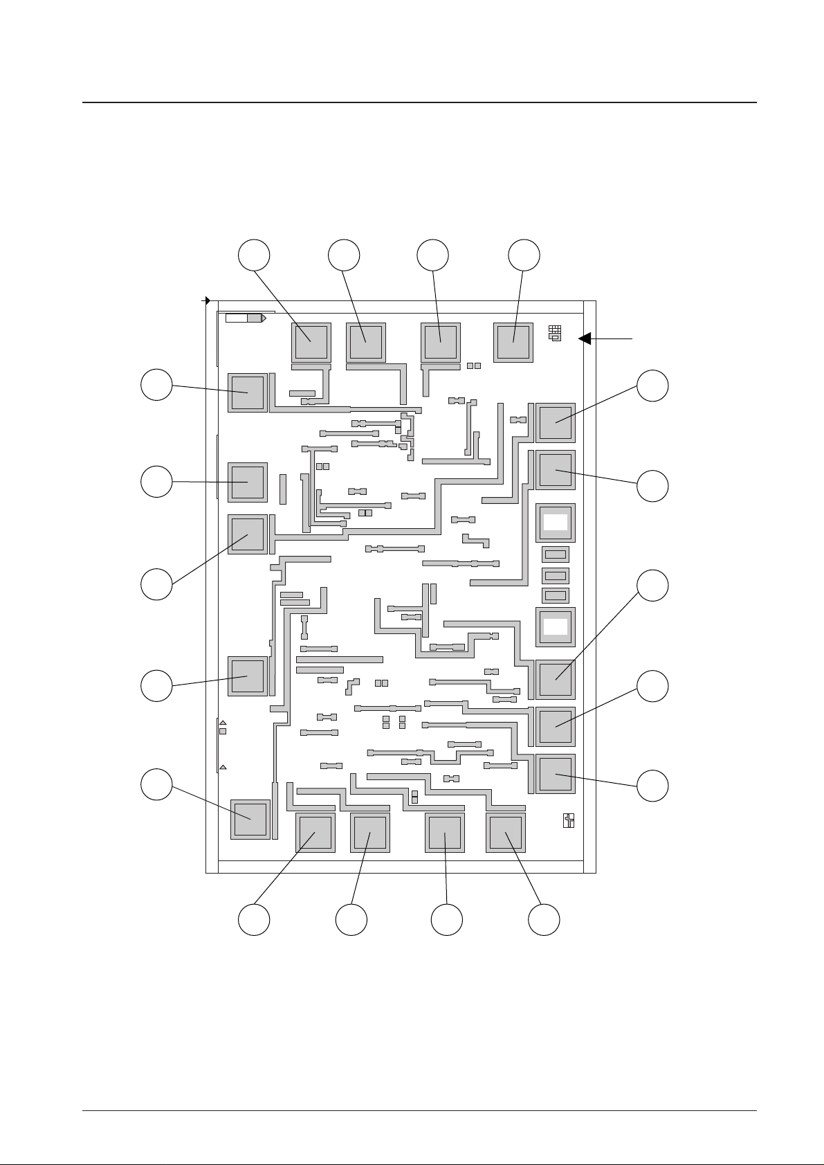
Metal Pattern Figure
No. 6310-4/14
LA1650, 1650C
2 1 18 17
16
1A1650
X : 1.41
Y : 2.06
15
14
13
12
111098
7
6
5
4
3
Pattern
Chip size
1A1650
A12842
NC
NC
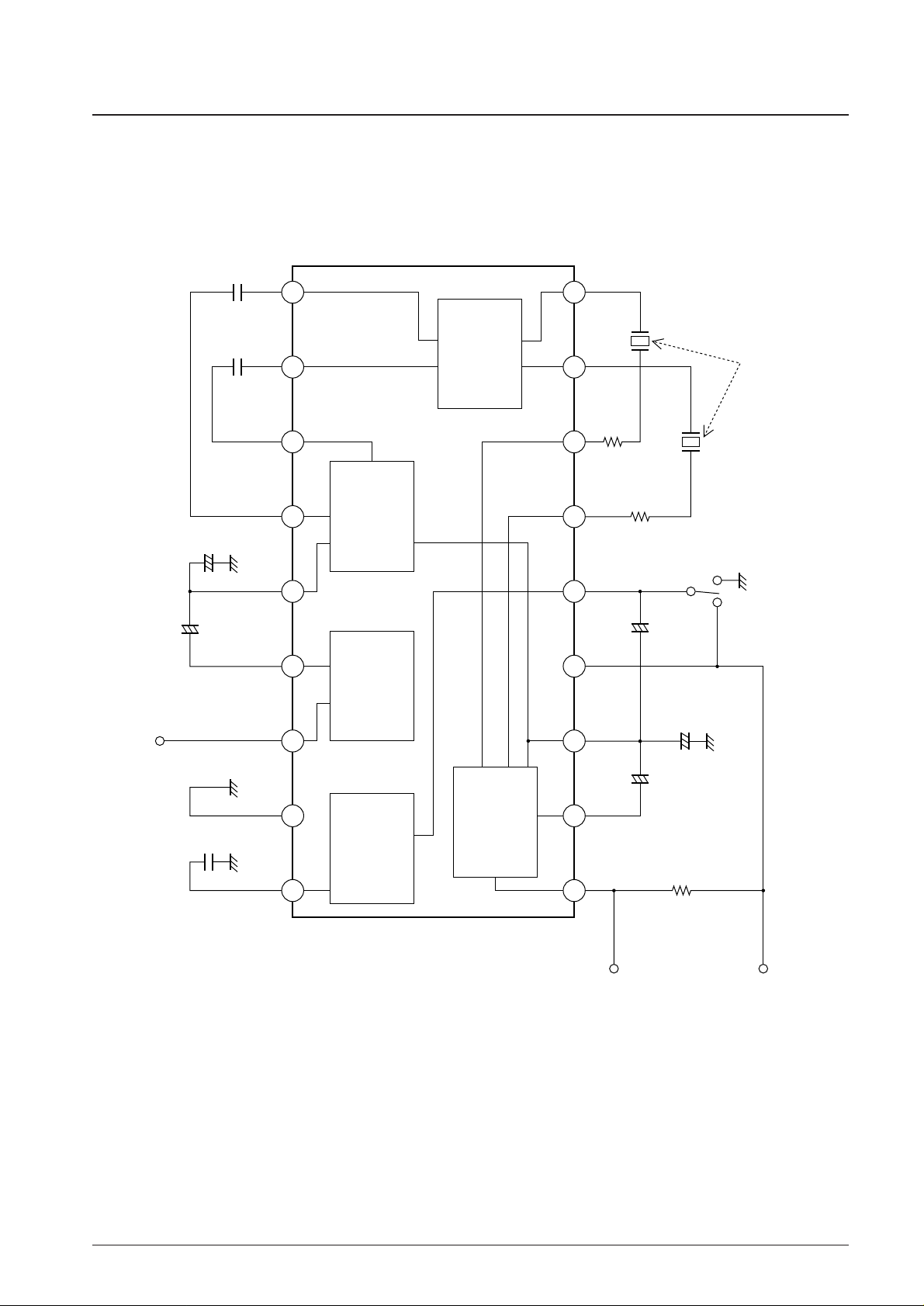
Block Diagram and Test Circuit
No. 6310-5/14
LA1650, 1650C
1
Input
V
CC
2
10µF22µF
10µF
22µF
0.015µF
TCO
1MΩ
1MΩ
1000pF
1000pF
Power ON Standby
40 kHz crystal
100µF
3 4 5 6 7 8 9
18 17 16 15 14 13 12 11 10
AMP(1)
REG DEC
AMP(2)
REC
51Ω
+
+
+
+
+
A12758
 Loading...