SANYO LA1225M Datasheet

Ordering number : ENN6017
32400TN (OT) No. 6017-1/8
Functions
• IF amplifier
• Quadrature detector
• Signal meter
•SD
• IF buffer
Features
• Low-voltage operation (1.8 V or higher)
• Supports electronic tuning systems (provides built-in SD
output and IF count output functions)
• FM detector circuit accepts an even wider input
frequency range. (Supports the use of an external phase
capacitor.)
• Miniature package: MFP-10S
Package Dimensions
unit: mm
3086A-MFP10S
1
10
5
6
0.55
1.8max
1.00.35
5.1
0.15
6.4
1.5
0.1
4.4
5.15 0.625
SANYO: MFP10S
[LA1225M]
LA1225M
SANYO Electric Co.,Ltd. Semiconductor Company
TOKYO OFFICE Tokyo Bldg., 1-10, 1 Chome, Ueno, Taito-ku, TOKYO, 110-8534 JAPAN
FM IF Detector IC
Monolithic Linear IC
Any and all SANYO products described or contained herein do not have specifications that can handle
applications that require extremely high levels of reliability, such as life-support systems, aircraft’s
control systems, or other applications whose failure can be reasonably expected to result in serious
physical and/or material damage. Consult with your SANYO representative nearest you before using
any SANYO products described or contained herein in such applications.
SANYO assumes no responsibility for equipment failures that result from using products at values that
exceed, even momentarily, rated values (such as maximum ratings, operating condition ranges, or other
parameters) listed in products specifications of any and all SANYO products described or contained
herein.
Parameter Symbol Conditions Ratings Unit
Maximum supply voltage V
CC
max 9.0 V
Allowable power dissipation Pd max Ta ≤ 80°C 100 mW
Operating temperature Topr –20 to +80 °C
Storage temperature Tstg –55 to +150 °C
Specifications
Maximum Ratings at Ta = 25°C
Parameter Symbol Conditions Ratings Unit
Recommended supply voltage V
CC
3.0 V
Operating supply voltage range V
CC
op 1.8 to 8.0 V
Operating Conditions at Ta = 25°C

No. 6017-2/8
LA1225M
Parameter Symbol Conditions
Ratings
Unit
min typ max
Current drain I
CCO
No input 3.0 4.0 5.0 mA
Demodulator output V
O
100 dBµ, 100% mod., fm = 1 kHz 70 150 220 mV
Total harmonic distortion THD 100 dBµ, 100% mod., fm = 1 kHz 0.5 0.8 %
Signal-to-noise ratio S/N 100 dBµ, 100% mod., fm = 1 kHz 65 73 dB
3 dB sensitivity –3 dBL.S
100 dBµ, 100% mod.,
19 28 37 dBµ
fm = 1 kHz output reference, when the input is –3 dB
SD sensitivity SD
ON
0% mod. 35 50 65 dBµ
IF counter buffer output V
IFBuff
100 dBµ 90 130 170 mV
Operating Characteristics at Ta = 25°C, VCC= 3.0 V, fc = 10.7 MHz
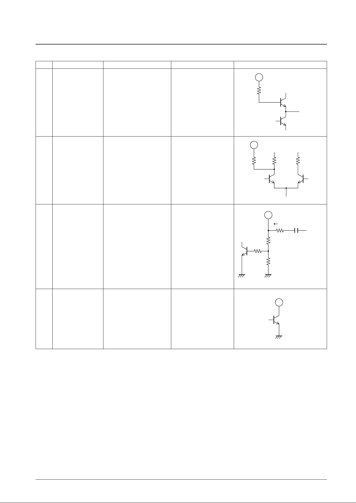
Pin Functions and No-Signal Voltage at VCC= 3.0 V
Pin No. Function Notes No-signal voltage (V) Equivalent circuit
Input impedance
R
IN
= 330 Ω
1.21 IF input
1
2
R
IN
A11506
Vreg = 1.2 V 1.22 Reg
2
A11507
03 GND
Open collector output
The SD sensitivity can be adjusted
with an external resistor
connected to this pin.
0.14 S-meter output
4
A11508
3.05
V
CC
Output impedance
R
OUT
= 3 kΩ
1.56 Demodulated output
6
R
OUT
A11509
Continued on next page.

No. 6017-3/8
LA1225M
Continued from preceding page.
Pin No. Function Notes No-signal voltage (V) Equivalent circuit
The detector coil is inserted
between pin 7 and pin 5 (V
CC
).
3.07 DET
7
A11510
Pin 8 and pin 7 (DET) are
connected through a capacitor.
2.88 Limiter amplifier output
8
A11511
The IF buffer output is turned on
when the voltage applied to the
pin is the recommended 1.5 V or
higher.
09
IF buffer
(Also used for control SW)
9
A11512
Control SW
IF buffer output
This is an active-low output.
This is an open-collector output
and can directly drive an LED.
(I
C
max = 20 mA)
1.610 SD
10
A11513
 Loading...