

SANYO LA1193V, LA1193M Datasheet
Monolithic Linear IC
Ordering number : EN4715A
31097HA (OT)/61094TH(OT) A8-9997 No. 4715-1/21
LA1193M, 1193V
SANYO Electric Co.,Ltd. Semiconductor Bussiness Headquarters
TOKYO OFFICE Tokyo Bldg., 1-10, 1 Chome, Ueno, Taito-ku, TOKYO, 110 JAPAN
High-Performance FM Front End for Car Radios
Overview
The LA1193M and LA1193V are front-end ICs developed
for use in car radios. It incorporates an extremely wide
dynamic range mixer and a new AGC system consisting
of a dual-system wide-band AGC and a new keyed AGC
to provide excellent interference suppression
characteristics.
Functions
• Double-balance mixer
• Pin diode drive output
• Differential IF amplifier
• Dual-system wide-band AGC circuit
• Local buffer output
• 3D-AGC system
• FET gate drive AGC output
• IF amplifier gain control pin
Features
• Improved interference characteristics
— Expanded mixer input dynamic range
Mixer input usable sensitivity: 15 dBµ
Mixer input I.M. QS: 90 dBµ
(The dynamic range has been increased by 6 dB
over the earlier LA1175M.)
— Development of a new wide-band AGC circuit
Improved interference characteristics for both nearchannel interference and far-channel interference
Improved interference characteristics for the TV band
— Development of a 3D-AGC system
The adjacent channel two-signal interference
characteristics can be effectively improved without
degrading the strong-field three-signal interference
characteristics during keyed AGC operation.
• Improved stability design
— AGC circuit local oscillator isolation
Measures were taken to prevent the deterioration of
AMR, noise level, THD and other characteristics
during AGC operation.
— AGC circuit incorrect operation measures
The LA1193M provides methods to prevent
incorrect operation due to local oscillator injection
and loss of DC balance.
• Improved temperature characteristics
— Conversion gain
— AGC sensitivity
— Antenna damping drive output current
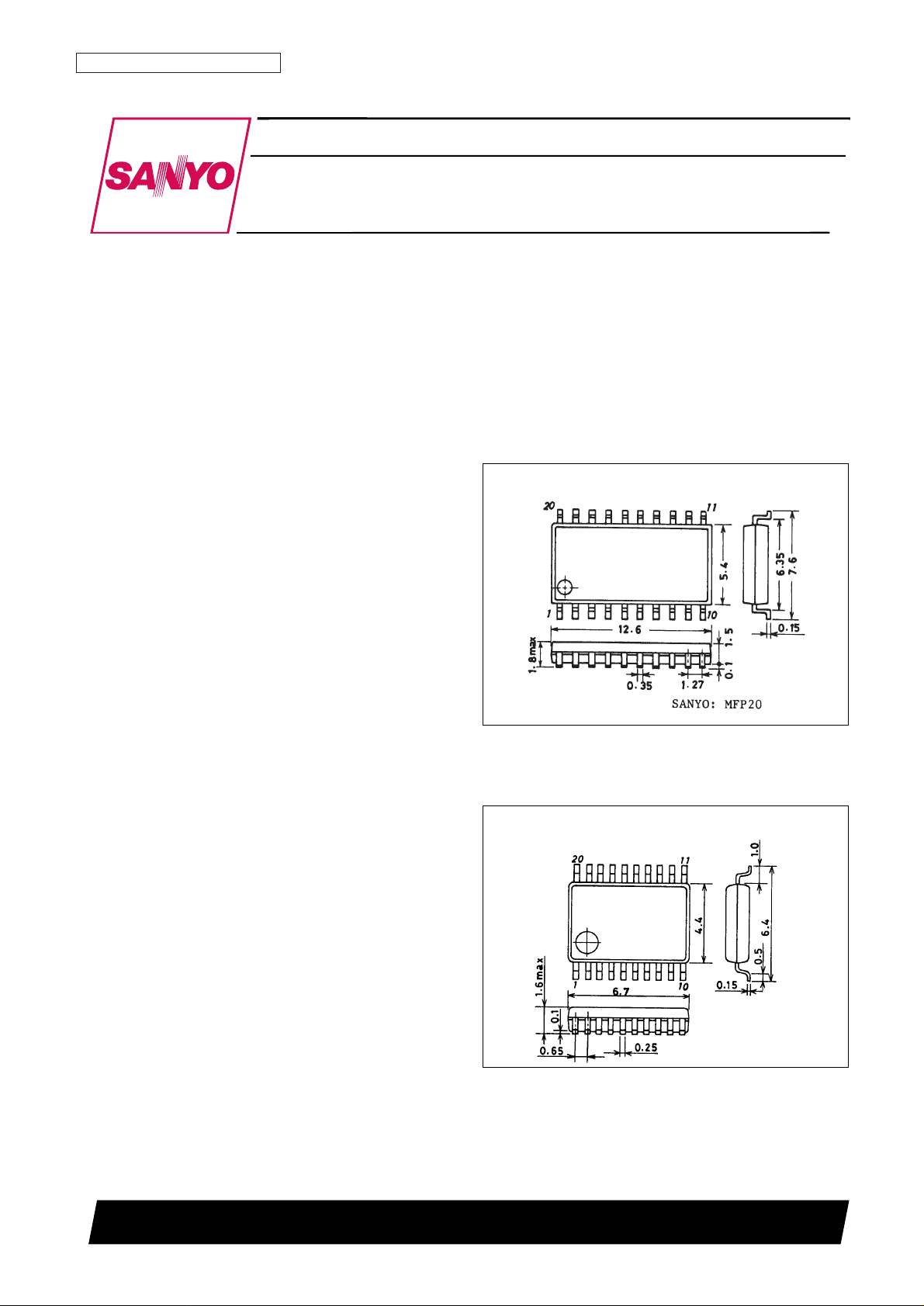
Package Dimensions
unit: mm
3036B-MFP20
unit: mm
3179A-SSOP20
[LA1193M]
[LA1193V]
SANYO: SSOP20
Specifications
Maximum Ratings at Ta = 25°C
Note: * Connect a resistor (up to 10 kΩ) between pins 17 and 19.
Operating Conditions at Ta = 25°C
Operating Characteristics at Ta = 25°C, VCC= 8.0 V, in the specified test circuit, f = 88 MHz, f
OSC
= 77.3 MHz
Note: Values in parenthesis are for LA1193V.
No. 4715-2/21
LA1193M, 1193V
Parameter Symbol Conditions Ratings Unit
Maximum supply voltage
V
CC
max VCCfor pins 5 and 17 9 V
V
CC
max mix VCCfor pins 10 and 11 15 V
Pd max
LA1193M: (Ta ≤ 70°C)
500 mW
Allowable power dissipation
Mounted on a 41
× 30 × 1.1 mm3glass-Epoxy board
Pd max
LA1193V: (Ta ≤ 70°C)
500 mW
Mounted on a 23 × 36 × 1.6 mm
3
glass-Epoxy board
Operating temperature Topr * –40 to +85 °C
Storage temperature Tstg –40 to +125 °C
Parameter Symbol Conditions
Ratings
Unit
min typ max
Current drain I
CCO
No input, V
CONT
= 0 V 19 24 29 mA
Antenna damping current ANT-DI 88 MHz, 100 dBµ, V
CONT
= 4.0 V 7.0 9.5 12.5 mA
AGC high voltage V
AGC-H
88 MHz, 0 dBµ, V
CONT
= 4.0 V 7.6 7.9 V
AGC low voltage V
AGC-L
88 MHz, 100 dBµ, V
CONT
= 4.0 V 0.4 0.9 V
Saturation output voltage V
OUT
88 MHz, 110 dBµ, V
CONT
= 4.0 V 97 110 dBµ
–3 dB limiting sensitivity Vi-Limit 88 MHz, 110 dBµ, V
CONT
= 4.0 V 78 85 92 dBµ
Conversion gain A. V 88 MHz, 75 dBµ, V
CONT
= 4.0 V 98 101 104 dBµ
Local buffer output V
OSC
-Buff No input, no modulation 105 109 dBµ
Narrow V
AGC-ON
V-NAGC
88 MHZ, V
CONT
= 4.0 V, at an input level 73 80 87 dBµ
such that V
AGC-OUT
is 2 V or less (76) (83) (90)
Wide V
AGC-ON
V-WAGC
88 MHZ, V
CONT
= 0 V, at an input level
97 101 105 dBµ
such that V
AGC-OUT
is 2 V or less
88 MHZ, V
CONT
variable, with 95 dBµ
3D-AGC-ON V3D-AGC
being the V
CONT
voltage input such that
0.4 0.6 0.8 V
V
AGC-OUT
switches from high to low and
2.0 V as the V
AGC
threshold value.
Parameter Symbol Conditions Ratings Unit
Recommended supply voltage V
CC
8.0 V
Operating supply voltage range V
CC
op 7.6 to 9 V
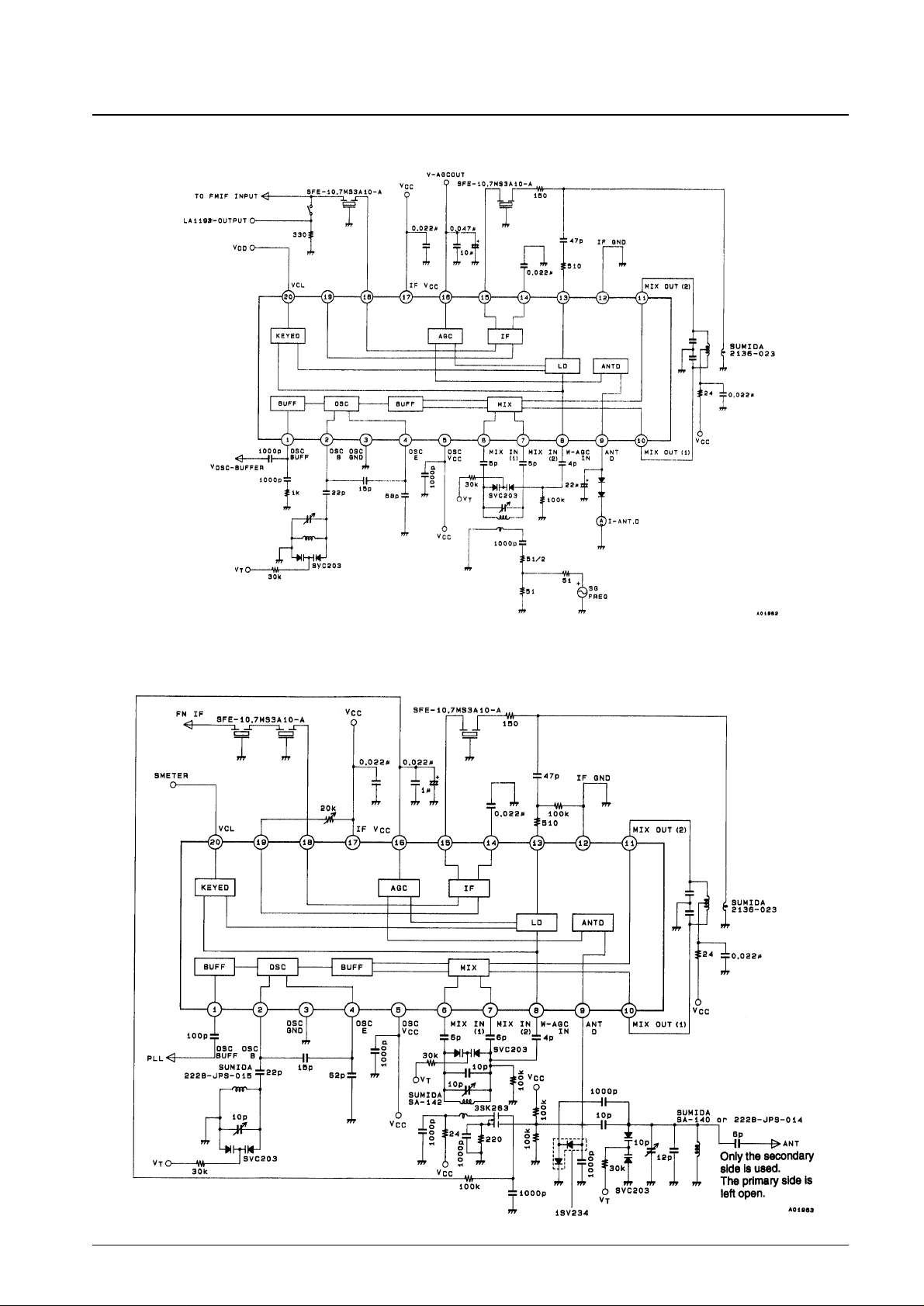
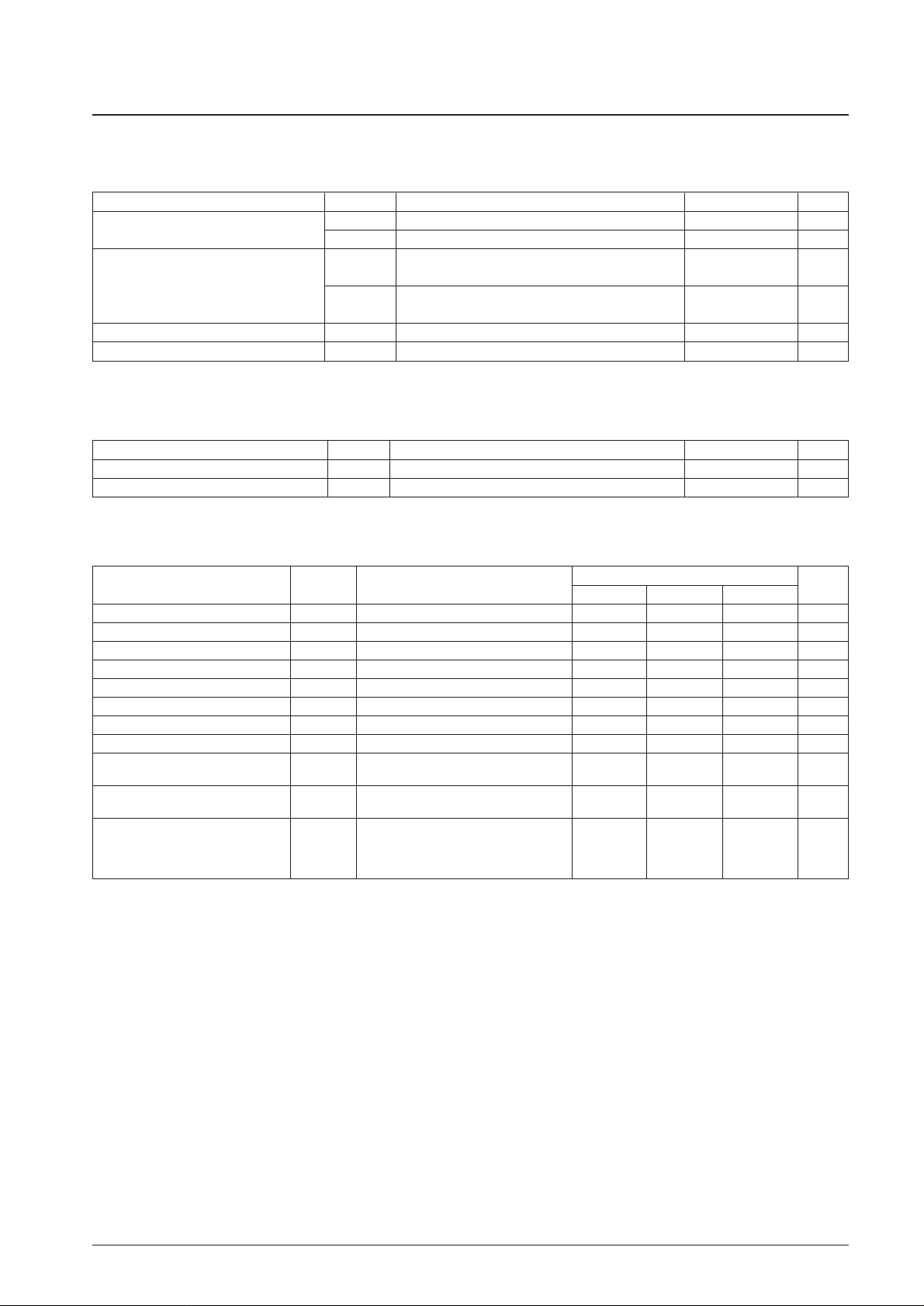
Block Diagram and Test Circuit Diagram
Application Circuit: USA and Europe
No. 4715-3/21
LA1193M, 1193V
Unit (Resistance: Ω, Capacitance: F)
Unit (Resistance: Ω, Capacitance: F)
Application Circuit: Japan
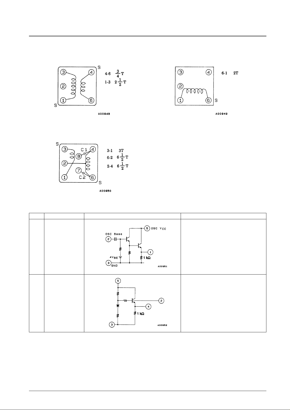
Coil Specifications
Coils Manufactured by Sumida Electronics
Japan band RF coil SA-129 or SA-143 Japan oscillator coil SA-125
Japan antenna coil SA-123 or SA-144 US band RF coil SA142 or SA-250
No. 4715-4/21
LA1193M, 1193V
Continued on next page.
Unit (Resistance: Ω, Capacitance: F)
Continued from preceding page.
US band antenna coil SA-140 or SA-231 US band oscillator coil SA-278
Mixer coil (for both bands) SA-266
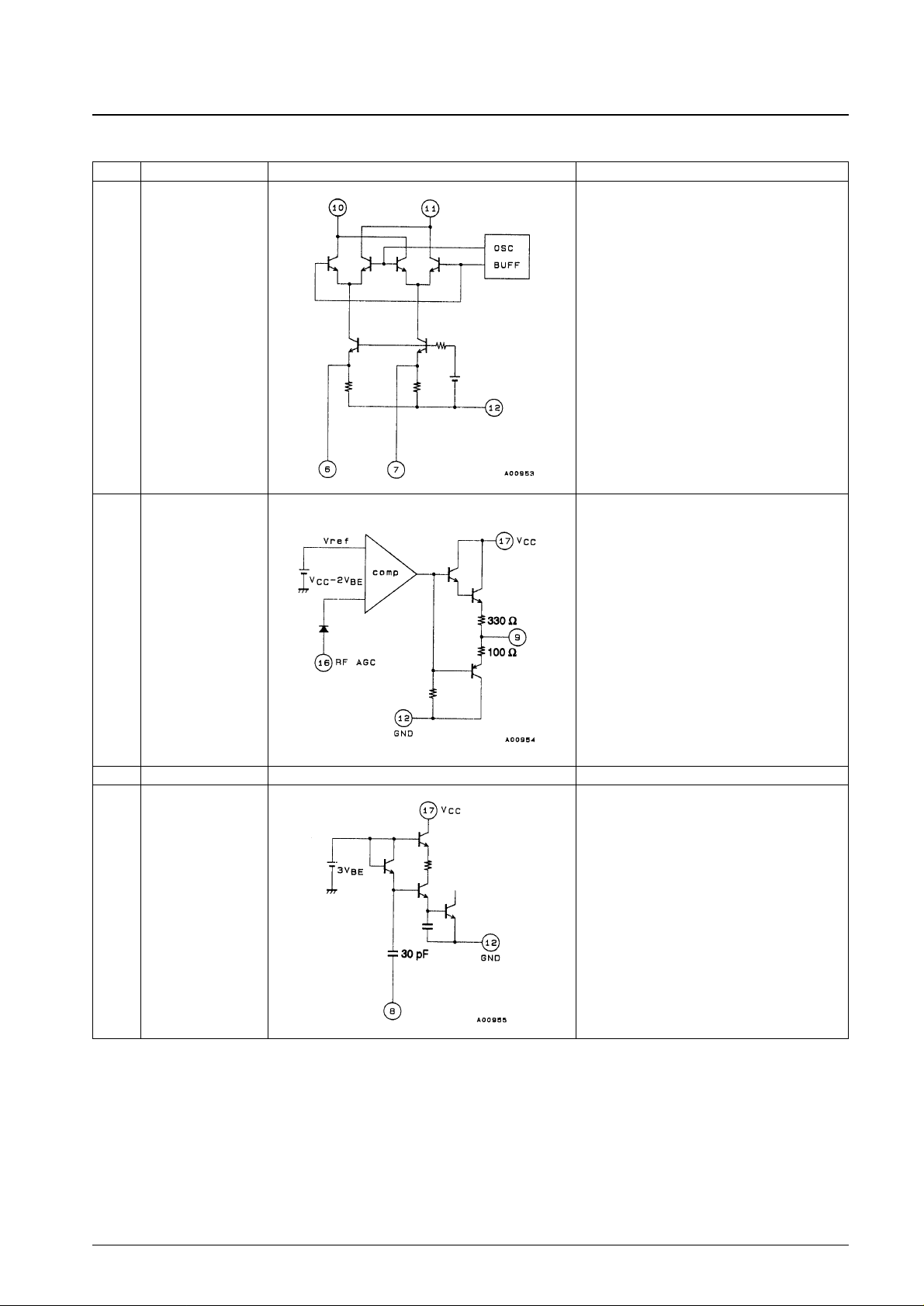
Pin Functions
No. 4715-5/21
LA1193M, 1193V
Pin No. Function Equivalent circuit Note
1
2
3
4
5
OSC BUFF
OSC Tr. base
OSC GND
OSC Tr. emitter
OSC V
CC
Colpitts oscillator
Continued on next page.
Continued from preceding page.
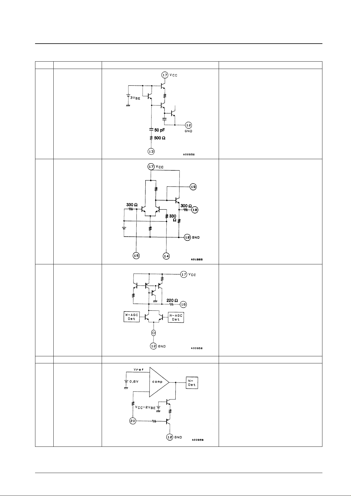
No. 4715-6/21
LA1193M, 1193V
Pin No. Function Equivalent circuit Note
6
7
10
11
9
12
8
Mix input (1)
Mix input (2)
Mix out (1)
Mix out (2)
Antenna damping
drive output
IF GND
W-AGC input
Mixer input usable sensitivity
15 dBµ
Mixer input I.M. QS
90.5 dBµ
(6.5 dB higher than previous products)
Conversion gain
15 dB
Input impedance
25 Ω
I
ANTD
= 10 mA
Since the DC cut capacitor is provided on-chip in the
pin internal circuit, we have taken steps to prevent
incorrect AGC operation due to inter-pin leakage
currents.
Continued on next page.
Continued from preceding page.
No. 4715-7/21
LA1193M, 1193V
Pin No. Function Equivalent circuit Note
13
14
15
18
19
16
17
20
N-AGC input
IF AMP bypass
IF AMP input
IF AMP output
IF AMP gain adjust
RF AGC output
IF, AGC, V
CC
Keyed AGC input
Since the DC cut capacitor is provided on-chip in the
pin internal circuit, we have taken steps to prevent
incorrect AGC operation due to inter-pin leakage
currents.
IF gain: 25 dB
Input and output impedances of 330 Ω
The IF gain can be adjusted by inserting a resistor
between pins 17 and 19.
The gain is at its maximum when there is no resistor
inserted.
MOSFET
Second gate control
Controls the narrow AGC.
 Loading...