

SANYO LA1145M, LA1145 Datasheet
Ordering number: EN 2725A
Monolithic Linear IC
LA1145, 1145M
FM IF System (Quadrature Detector) for Car Radio
Features
1. On-chip IF count buffer circuit and microprocessorcontrolled switch circuit for ETR.
2. Compared to the LA1140, the LA1145, 1145M offer:
1 Improved signal meter output linearity;
2 Improved band mute temperature stability;
3 Improved S/N ratio;
4 Improved sound quality at weak signal input when
noise is present, and;
5 Improved AMR characteristics during weak signal
input.
3. Reduced parts’ count simplifies design:
1 On-chip IF count buffer circuit;
2 On-chip SD circuit — sensitivity can be set
independently of soft mute characteristics, and;
3 Variable S-meter gradient — three pin S-meter output
(pins 5, 16 and 17) facilitates independent control of
SNC and HCC.
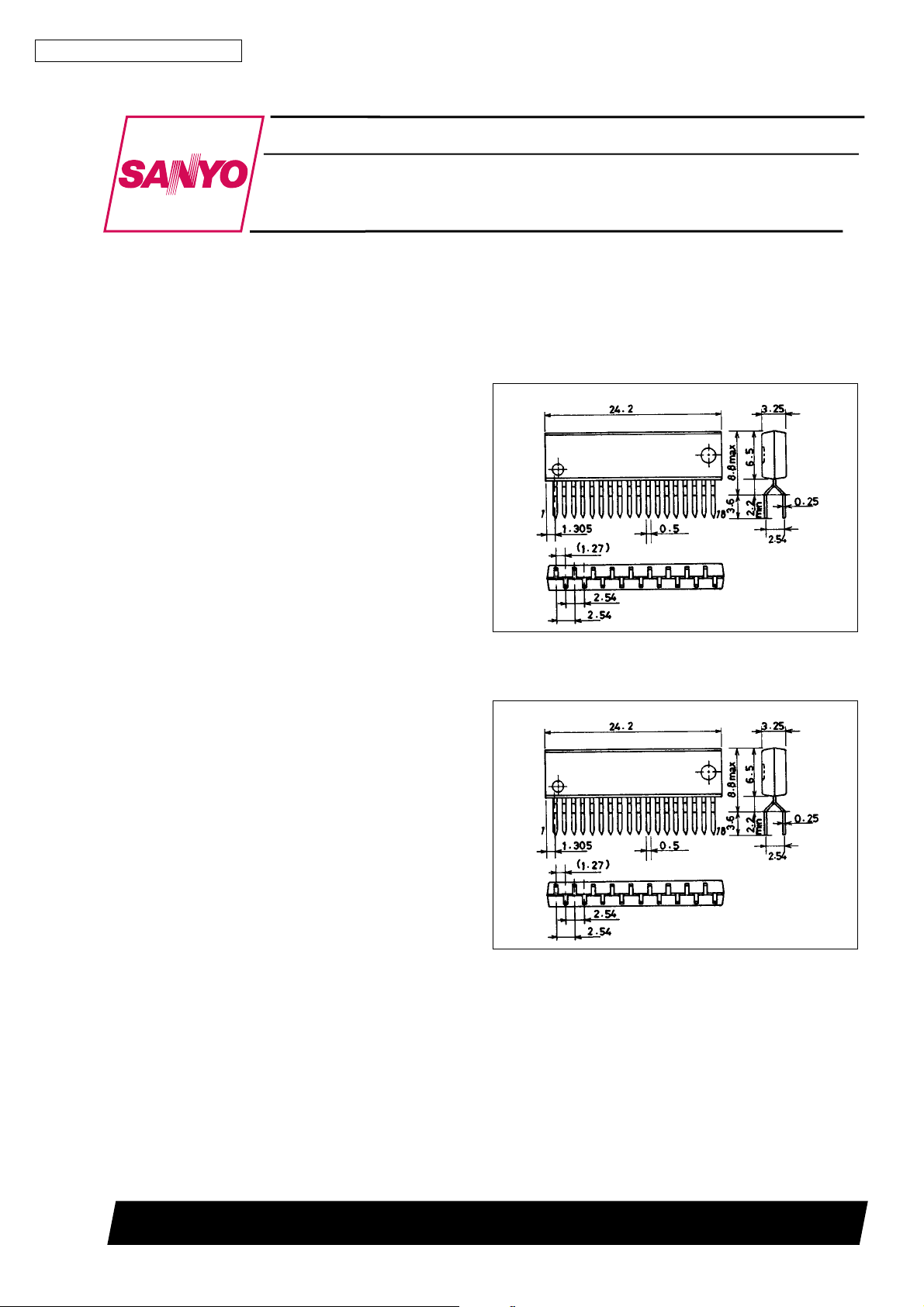
Package Dimensions
unit : mm
3115-SIP18Z
[LA1145]
SANYO : SIP18Z
unit : mm
3036B-MFP20
[LA1145M]
SANYO: MFP20
SANYO Electric Co.,Ltd. Semiconductor Bussiness Headquarters
TOKYO OFFICE Tokyo Bldg., 1-10, 1 Chome, Ueno, Taito-ku, TOKYO, 110 JAPAN
93097HS(II)/3132TS/2118TA No.2725-1/17
LA1145, 1145M
Specifications
[LA1145]
Maximum Ratings atTa=25°C
Parameter Symbol Conditions Ratings Unit
Maximum supply voltage V
Maximum supply current I
Allowable power dissipation Pd max Ta = 65 °C 630 mW
Operating temperature Topr –20 to +70 °C
Storage temperature Tstg –40 to +150 °C
Operating Conditions atTa=25°C
Parameter Symbol Conditions Ratings Unit
Recommended supply voltage V
Operating voltage range V
Operating Characteristics at Ta = 25°C,VCC=8V,fin= 10.7 MHz
max Pin 12 14 V
CC
max Pin 12 45 mA
CC
Ta = 70°C 590 mW
8V
7.5 to 14 V
CC
CC
op
Parameter Symbol Conditions min typ max Unit
Quiescent current I
Current drain I
Demodulation output V
Total harmonic distortion THD
Signal-to-noise ratio S/N V
Input limiting voltage V
Muting sensitivity V
Muting bandwidth BW(mute) V
Muting attenuation
Signal strength indication output
Muting drive output
AM rejection ratio AMR V
Offset voltage
SD sensitivity V
IF count output level V
CCO
CC
O
(lim) 400 Hz tone, 100%, soft mute ON 34 40 46 dBµ
IN
(mute) V15= 2 V 30 36 42 dBµ
IN
mute(1)
mute(2)
V
16-0
V
16-50
V
16-70
V
16-100
V
15-0
V
15-100
V
7-11
V
8-11
SD
(IF) VIN= 100 dBµ, pin 13, CL= 10 pF 110 180 280 mVrms
IN
[LA1145M]
VIN= 0 dBµ 18 26 36 mA
VIN= 100 dBµ 20 29 36 mA
VIN= 100 dBµ, 400 Hz tone, 100% 300 400 520 mVrms
= 100 dBµ, 400 Hz tone, 100%,
V
IN
single tuning coil
= 100 dBµ, 400 Hz tone, 100% 79 85 dB
IN
= 100 dBµ, V18% 0.3 V 140 190 280 kHz
IN
V
= 100 dBµ, V15=2V,
IN
400 Hz tone, 100%
= 100 dBµ, V15=4V,
V
IN
400Hz tone, 100%
VIN= 0 dBµ, RA=10kΩ, pin 16 0 0.1 0.4 V
VIN= 50 dBµ, RA=10kΩ, pin 16 1.4 2.3 3.2 V
VIN= 70 dBµ, RA=10kΩ, pin 16 2.5 4.5 5.5 V
VIN= 100 dBµ, RA=10kΩ, pin 16 5.0 5.5 6.0 V
VIN= 0 dBµ, pin 15 4.0 4.8 5.5 V
VIN= 100 dBµ, pin 15 0 0 0.3 dB
= 100 dBµ, 1 kHz tone, 30% AM 57 70 dB
IN
VIN= 0 dBµ, pins 7 to 11 –0.25 0 +0.25 V
VIN= 0 dBµ, pin 8 to 11 –0.5 0 +0.5 V
Pin 18 50 58 66 dBµ
0.3 0.8 %
10 15 20 dB
25 29 33 dB
Maximum Ratings atTa=25°C
Parameter Symbol Conditions Ratings Unit
Maximum supply voltage V
Maximum supply current I
Allowable power dissipation Pd max Ta = 70°C, mounted on PC board,
Operating temperature Topr –20 to +70 °C
Storage temperature Tstg –40 to +125 °C
max Pin 13 14 V
CC
max Pin 13 45 mA
CC
independent IC
Ta = 25°C, mounted on PC board,
Independent IC
630 mW
630 mW
No. 2725-2/17
LA1145, 1145M
Operating Conditions at Ta = 25°C
Parameter Symbol Conditions Ratings Unit
Recommended supply voltage V
Operating voltage range V
Operating Characteristics at Ta = 25 °C, VCC=8V,fin= 10.7 MHz
Parameter Symbol Conditions min typ max Unit
Quiescent current I
Current drain I
Demodulation output V
Total harmonic distortion THD
Signal-to-noise ratio S/N V
Input limiting voltage V
Muting sensitivity V
Muting bandwidth BW (mute) V
Muting attenuation
Signal strength
indication output
Muting drive output
AM rejection ratio AMR V
Offset voltage
SD sensitivity V
IF count output level
CC
op 7.5to 14 V
CC
CCO
CC
IN
(mute) V16= 2 V 30 36 42 dBµ
IN
mute (1)
mute (2)
V
17-0
V
17-50
V
17-70
V
17-100
V
16-0
V
16-100
V
8-12
V
9-12
SD
V
-On VIN= 100 dBµ, pin 14, CL= 10 pF 110 180 280 mVrms
IF
V
-OFF VIN= 100 dBµ, pin 14, CL=10pF 1 3 mVrms
IF
VIN= 0 dBµ 18 26 36 mA
VIN= 100 dBµ 20 29 40 mA
VIN= 100 dBµ, 400 Hz tone, 100% 300 400 520 mVrms
O
= 100 dBµ, 400 Hz tone, 100%,
V
IN
single tuning coil
= 100 dBµ, 400 Hz tone, 100% 79 85 dB
IN
(lim) 400 Hz tone, 100%, soft mute ON 34 40 46 dBµ
= 100 dBµ, V19% 0.3 V 140 190 280 kHz
IN
V
= 100 dBµ, V16=2V,
IN
400 Hz tone, 100%
= 100 dBµ, V16=4V,
V
IN
400 Hz tone, 100%
VIN= 0 dBµ, R16=10kΩ, pin 17 0 0.1 0.4 V
VIN= 50 dBµ, R16=10kΩ, pin 17 1.4 2.3 3.2 V
VIN= 70 dBµ, R16=10kΩ, pin 17 2.5 4.5 5.5 V
VIN= 100 dBµ, R16=10kΩ, pin 17 5.0 5.5 6.0 V
VIN= 0 dBµ, pin 16 4.0 4.8 5.5 V
VIN= 100 dBµ, pin 16 0 0 0.3 V
= 100 dBµ, 1 kHz tone, 30% AM 57 70 dB
IN
= 0 dBµ, pin 8 to 12 –0.25 0 +0.25 V
V
IN
VIN= 0 dBµ, pin 9 to 12 –0.5 0 +0.5 V
Pin 19 50 58 66 dBµ
8V
0.3 0.8 %
10 15 20 dB
25 29 33 dB
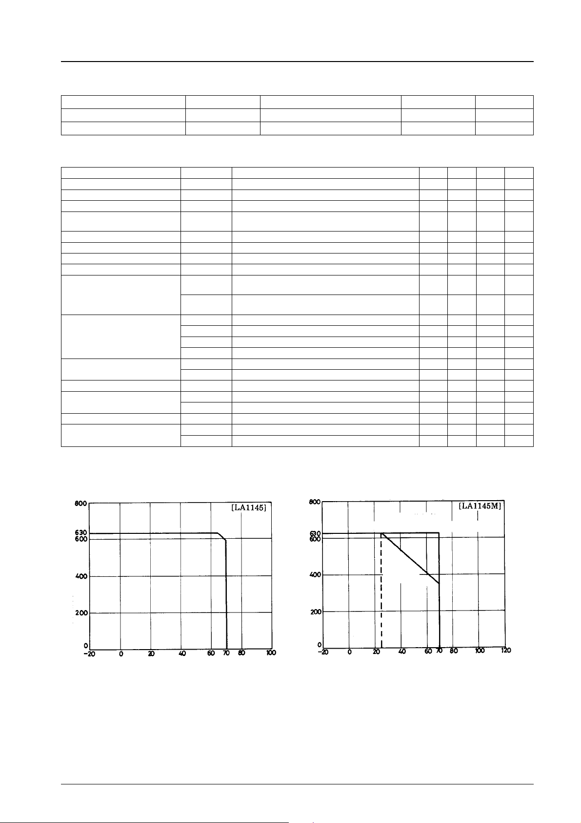
Allowable power dissipation, Pd max – mW
Pdmax–Ta Pdmax–Ta
Ambient temperature, Ta – °C
Allowable power dissipation, Pd max – mW
Mounted on PCB
(90 × 60 × 1.5 mm3glass epoxy
Independent
IC
Ambient temperature, Ta – °C
No. 2725-3/17
LA1145, 1145M
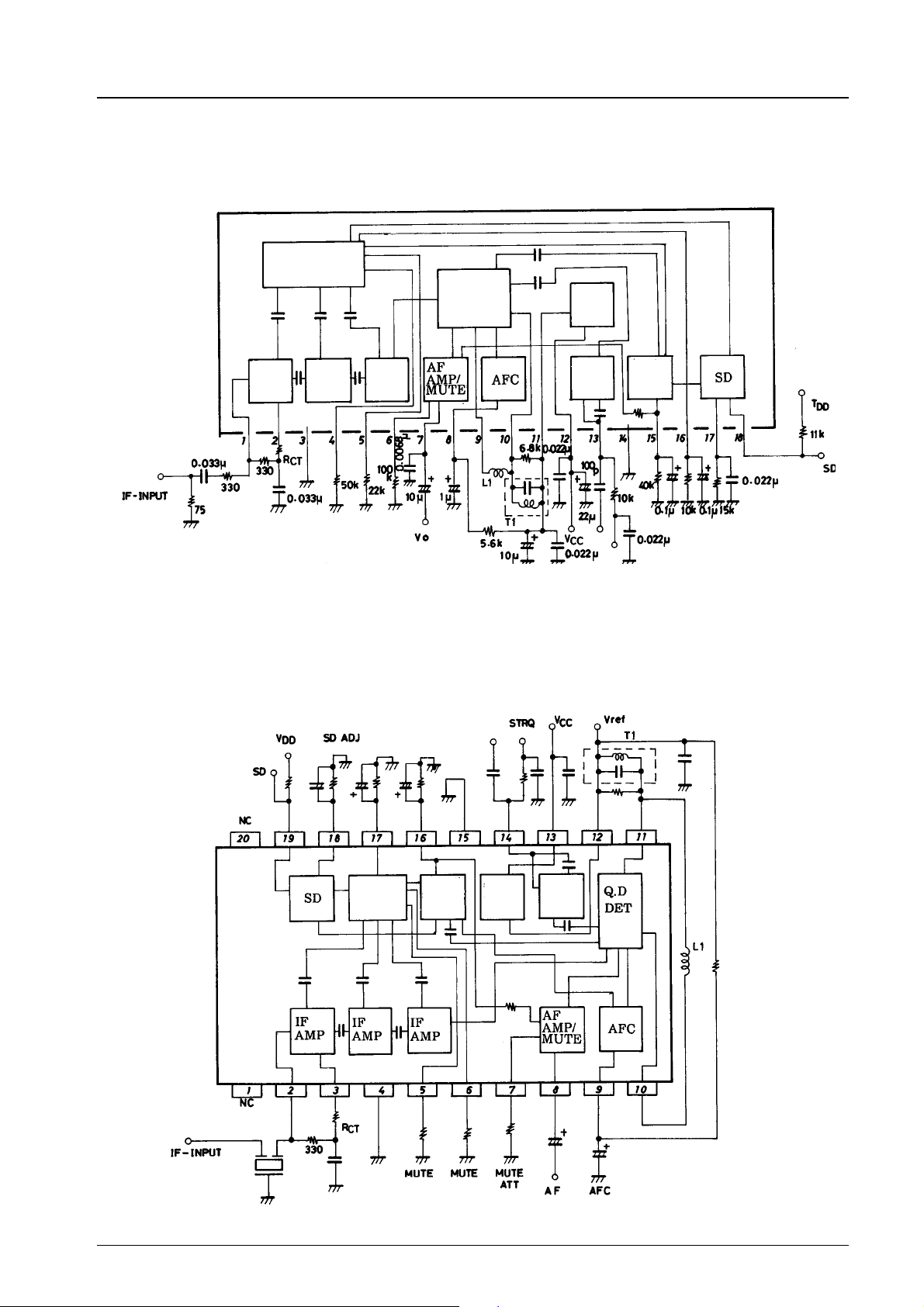
LA1145 Equivalent Circuit Block Diagram
S-meter detector
IF amp
IF amp
IF amp
LA1145M Equivalent Circuit Block Diagram
S-meter Mute
Quadrature
detector
driver
Voltage
regulator
IF
count
Hole
detector/
mute
driver
Unit (resistance: Ω, capacitance: F)
S-meter
detector
Hole
detector/
mute
driver
Start point Gradient
Voltage
regulator
IF
count
*R
is a resistor for variable gain.
CT
Normally 0 Ω.
No. 2725-4/17
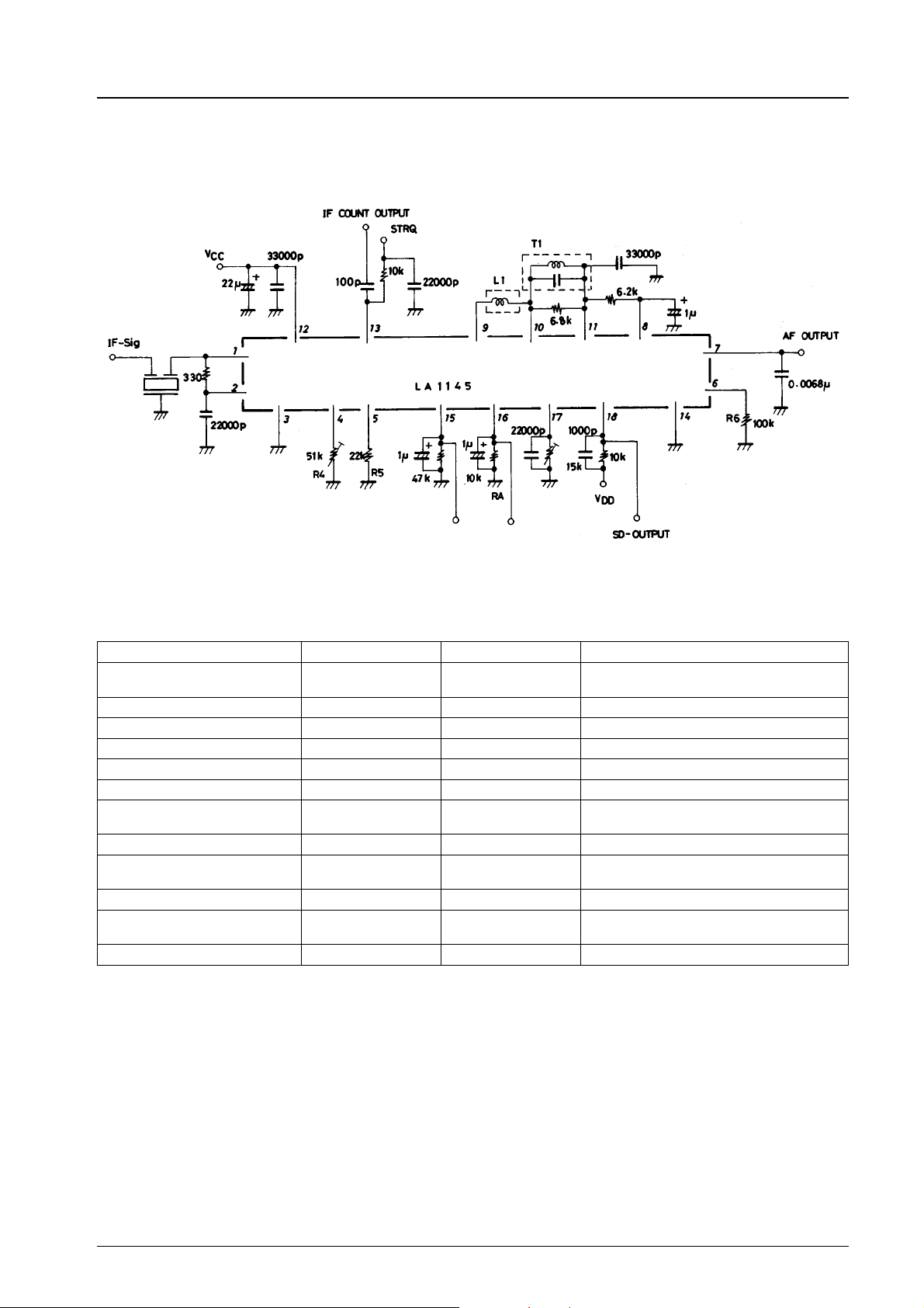
Sample Application Circuit
LA1145, 1145M
50 µs
DC
emphasis
capacitor
Mute driver
output
S-meter
output
Unit (resistance: Ω, capacitance: F)
LS1140 and LS1145 Compared
Parameter LA1140 LA1145 Remarks
Package SIP-16
IF amp, limiter Direct-coupled C-coupled
Quadrature detector jj
AF preamp jj
AFC output jj
Signal meter output j
Band muting j
IF count buffer output – j Common with STRQ
SD circuit – j
S/N 78 dBµ 86 dB
3 dBµ limiting sensitivity 25 dBµ (fixed) 25 to 40 dBµ
Weak signal noise output j
SIP-18Z
MFP-20
j Improved linearity, variable S-meter gradient
C
j
C
j
C
Improved temperature stability,
V
dependent
BE
For the LA1140, Coupled with the soft muting
function.
–3 dBµ limiting sensitivity variable,
independent of soft muting function
L1: 81N-014A (Sumida)
L2: 81N-014B (Sumida)
No. 2725-5/17
LA1145, 1145M
LA1145 Pin Description and Typical Voltages
Pin No. Typical Voltage (V) Description Remarks
1 2.6 IF input
2 2.6 IF amp bias
3 0.0 IF amp GND
4 4.0 Mute start control
5 0.2 Mute gradient control
6 2.1 Mute attenuation control
7 4.9 AF output
8 5.0 AFC output
9 4.8 IF output
10 4.8 Quadrature detection input
11 4.8 Voltage regulator output
12 8.0 V
13 0.1 IF count output, control
14 0.0 GND for detection circuit
15 4.8 Mute driver
16 0.2 S-meter output
17 0.2 SD sensitivity control
18 0.1 SD output Open collector
CC
LA1145M Pin Description and Typical Voltages
Pin No. Typical Voltage (V) Description Remarks
1–NC
2 2.6 IF input
3 2.6 IF amp bias
4 0.0 IF amp GND
5 4.0 Mute start control
6 0.2 Mute gradient control
7 2.1 Mute attenuation control
8 4.9 AF output
9 5.0 AFC output
10 4.8 IF output
11 4.8 Quadrature detection input
12 4.8 Voltage regulator output
13 8.0 V
14 0.1 IF count output, control
15 0.0 GND for detection circuit
16 4.8 Mute driver
17 0.2 S-meter output
18 0.2 SD sensitivity control
19 0.1 SD output Open collector
20 – NC
CC
No. 2725-6/17
 Loading...