

Page 1
Samsung Electronics 13-1
13. Circuit Operating Description
13-1 Introduction to the product
13-1-1 Introduction
SPIDER-X ; VP-X105 is equipped with a MICRO Compact Size NAND Flash Memory of 512MByte
(256MB, 1GByte) making this the first Built-in memory Chip Camcorder in the world. Product incorporates many
functions including Camcorder, DSC, MP3, Data storage, PC Camera and Voice Recorder. It records and plays
back VGA Size images using an MPEG4 format running at 30fps as a Tapeless Camcorder. Product is also
equipped with Memory Stick Pro Socket.
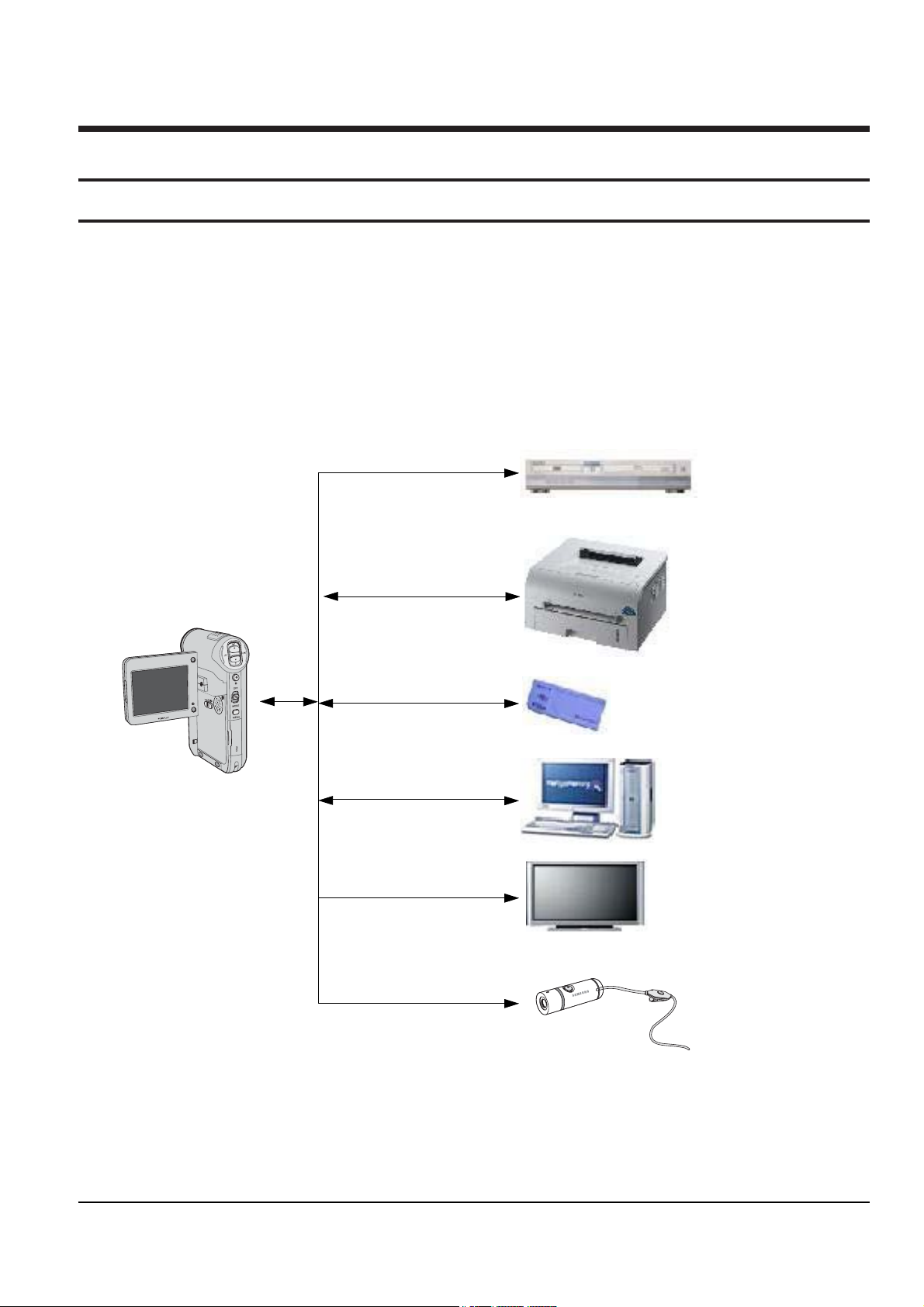
13-1-2 System structure
Fig. 13-1 System structure
Spider-X
Video/DVD
Printer
Memory Stick / Pro
Computer
Monitor
External-Camera
Page 2
Circuit Operating Description
13-2 Samsung Electronics
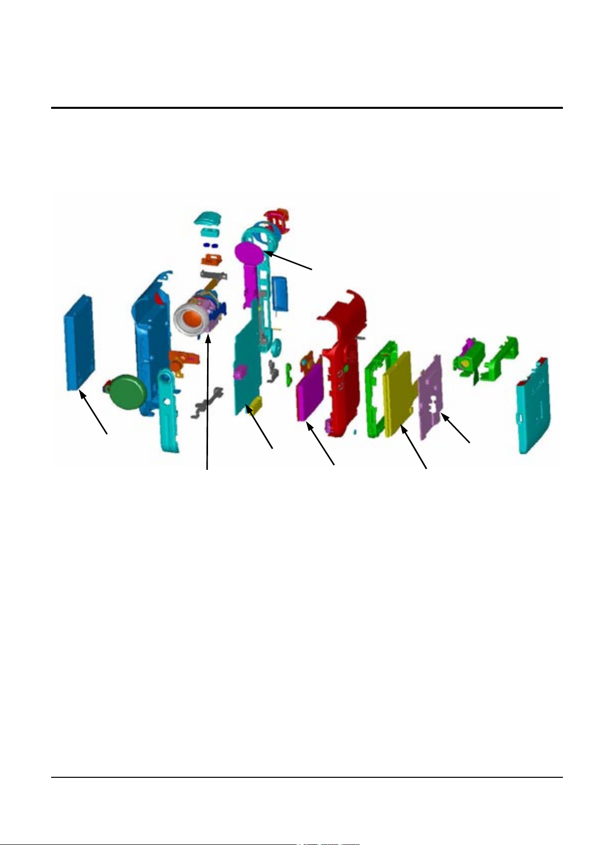
13-2 Structure
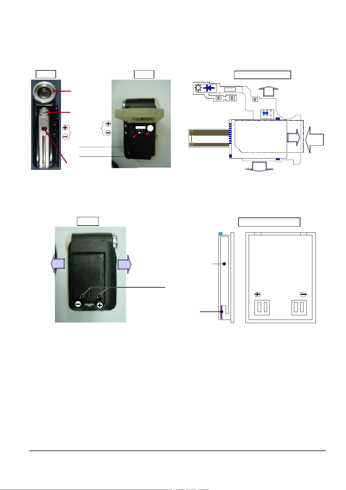
13-2-1 Product body
1) Entire structure
VP-X110/X105/X102 consists of Main Board, Right Ass'y, Left-Front Ass'y, Camera Lens Ass'y, Top Ass'y,Bottom
Ass'y,Rear Ass'y,LCD Ass'y in the Fig. 13-2
Fig. 13-2 Entire assembly structure
Battery
Lens Ass'y
Main PCB
Front-Left FPC
LCD Panel
LCD PCB
Rear
Page 3
Circuit Operating Description
Samsung Electronics 13-3
Ass'y Block Structure circuit
DSP DSP6
SYSCON Mode MICOM
AUDIO AUDIO CODEC,BEEP
Main Board
Camera CDS/AGC/AD,HALL/IRIS CTL,Zoom Motor Drive
DC/DC PWM,Battery DET,Charger
CODEC Encorder
Memory SDRAM,Nor-Flash(booting),Nand-Flash(storage),EEPROM
IN/OUT Video AMP,Video,Audio,HP Switching
EIS EIS Sensor,OP AMP
Left-Front S/W Volume Up/Down,Hold,LCD Detect
Others LED Strobo,MS Socket
Right Battey Housing Battery Housing
Camera Lens X10 Lens,OLPF,CCD,V-Drive
LCD
LCD Drive,LCD Panel,Hinge,LCD FPC,Display S/W
LCD on/off S/W,
Rear
S/W Zoom,Enter,Back,Power/Mode,REC,Menu
Display Power(RED),Charge(Green),Emergency(ORG blinking)
TOP Mic Cell
Bottom Tripod,I/O connector,Strap Ring
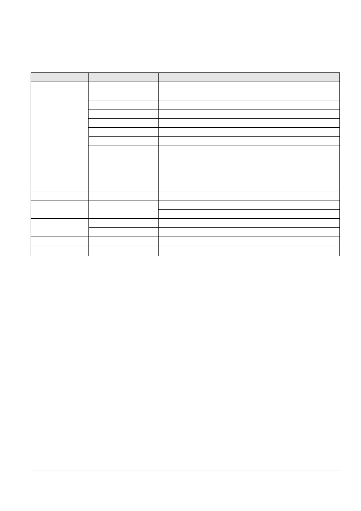
<Table 13-1 Block structure per an assembly>
2) Refer to the below table about block structure per assembly
Page 4
Circuit Operating Description
13-4 Samsung Electronics
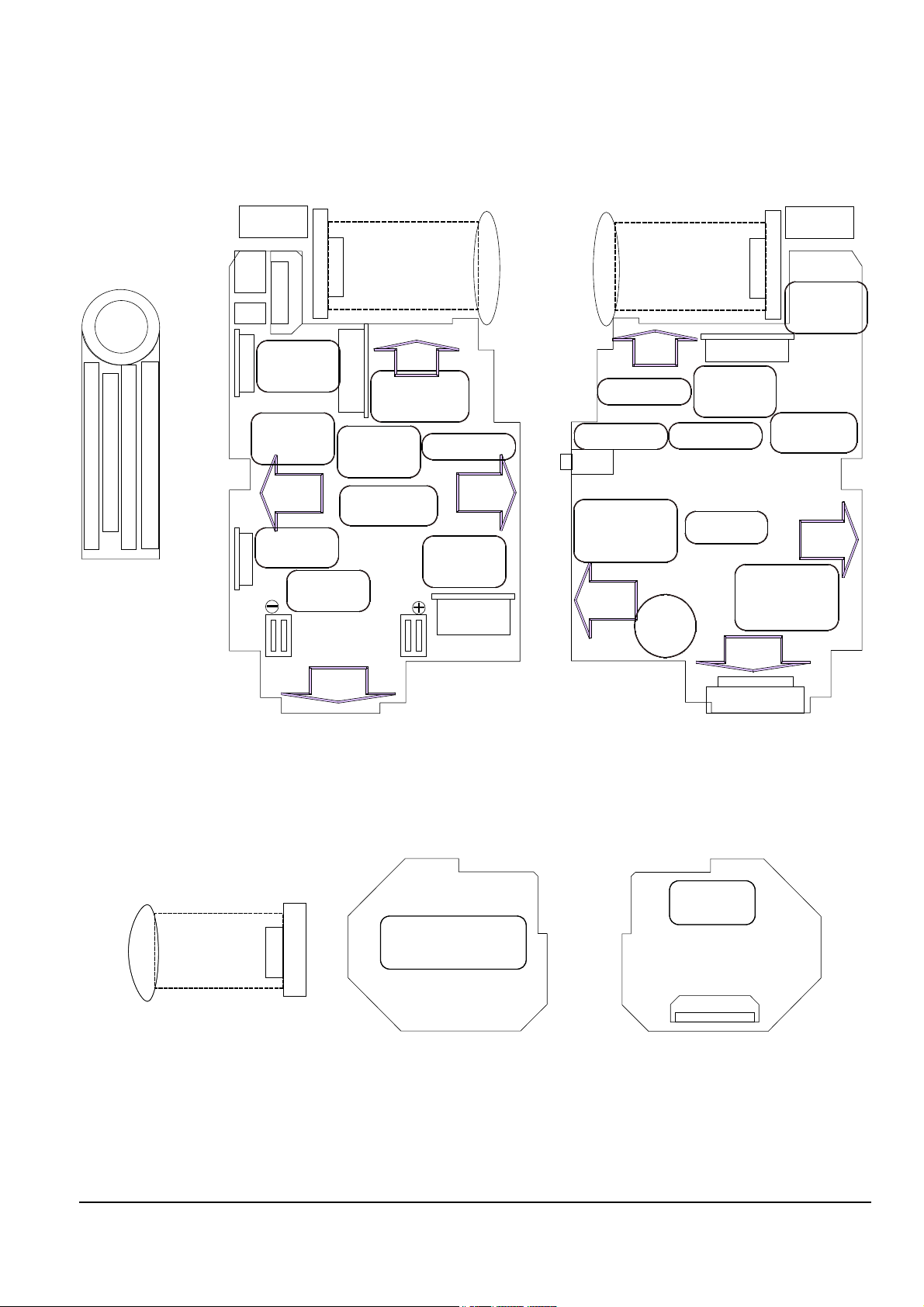
13-2-2 Board structure per an assembly
1) Board structure system and the Main PCB
Fig. 13-3 MAIN PCB structure
Rear
Side
B
A
T
T
E
R
Y
M
A
I
N
P
C
B
L
E
F
T
F
P
C
L
C
D
ASSY-MIC ASSY-MIC
LENS
ASS'Y
LENS
ASS'Y
C
C
D
P
C
B
C
C
D
P
C
B
C
C
D
C
C
D
X10
X10
Motor-Drive
(uPD16877)
Mic
(WAF 4P)
Speaker
WAF 2P
CCD
(FPC 18P)
Assy Rear
(FPC 10P)
JTAG
(FPC 8P)
Assy Lens
(FPC 20P)
Hall/Iris-CTL
(NJM2902V*2)
Top
Side
Top
Side
Rear
Side
Rear
Side
Front
Side
Front
Side
Bottom
Side
Bottom
Side
Lithium
Micom
(SYSCON)
(uPD78F0078Y)
DC/DC
(MX1576)
Assy LEFT
(FPC 14P)
Battery
Det/Charge
(LTC4503)
SDRAM (32MB)
(K4M563233D)
DSP6-Chip
(S5C7376X)
Encorder
(TW9220)
Video I/O-SW
(NJM2902V*2)
Audio I/O-SW
(FSAV330MTC)
HP I/O-SW
(FSAV330MTC)
Video AMP
(NJM2573V)
Nor-Flash (2MB)
(K8D1616UBA)
Right Side Main PCB
(Battery)
Left Side Main PCB
(LCD)
CDS/AGE/AD
(TLV990B)
LCD
(FPC 20P)
Audio CODEC
(AK4564)
EEPROM
(8KB) 0
A/V IN-OUT
EAR-OUT JACK
Nand-Flash
(256,512MB,1GB)
(K9F2G08UCM)
Video Beep
(ML2201-xxx)
Fig. 13-4 CCD PCB structure
X10
LENS
ASS'Y
C
C
D
C
C
D
P
C
B
Lens Side
CCD(1/6inch)
(NTSC:ICX440, 680,000)
(PAL :ICX441, 800,000)
Vetical Drive
(KS7221D)
Rear Side
FPC 19P
2) LENS Ass'y
Page 5
Circuit Operating Description
Samsung Electronics 13-5
Fig. 13-5 Left & Front structure
Front
Left
Left Front FPC
Lens(X10)
Flash LED
Volume
Hold S/W
Speaker
Earphone Out,
both A/V In-Out
Off-Lock
LED-Strobo
FPC Lead open
(+) (-)
Volume
Left-FPC A'ssy
(LCD)
LCD-Detect
Off<=>On
MS
insert
MS Socket
Rear
Side
Bottom
Side
Top
Side
HOLD
3) Left & Front
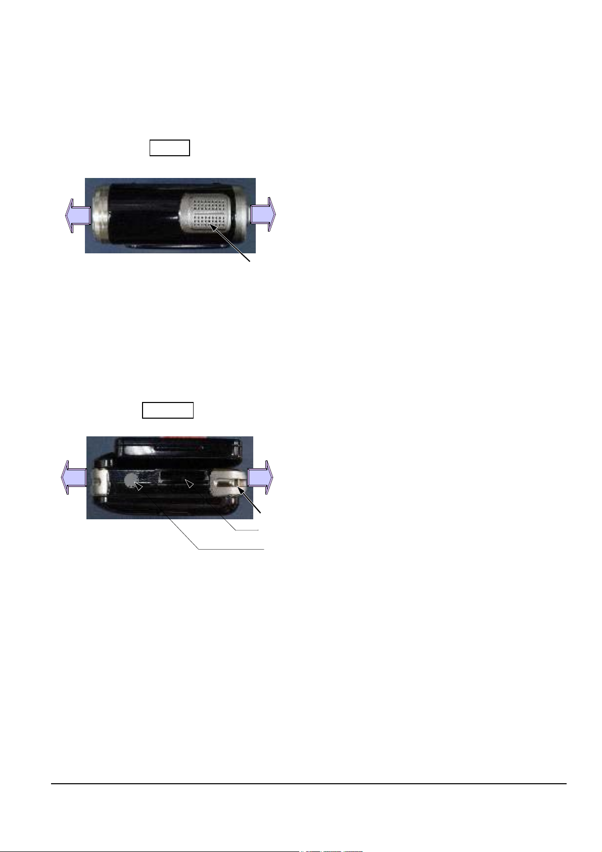
Fig. 13-6 Right structure
Right
Rear
Side
Front
Side
Bat-Terminal
PCB
Battery Cell
US473350
A7T(SONY)
Battery-Pack
back
1
23
4
4) Right
Page 6
Circuit Operating Description
13-6 Samsung Electronics
Fig. 13-7 LCD structure
LCD
LCD-PCB
Top
Side
Bottom
Side
Display
(Tact-SW)
(SW-Tact)
Display
LCD Panel
(ACX510BLM, 210,000)
To Panel
(FPC 24P)
To Panel
(Wire 2P)
To Main PCB
(FPC 20P)
LCD Drive
(CXM3004R)
5) LCD
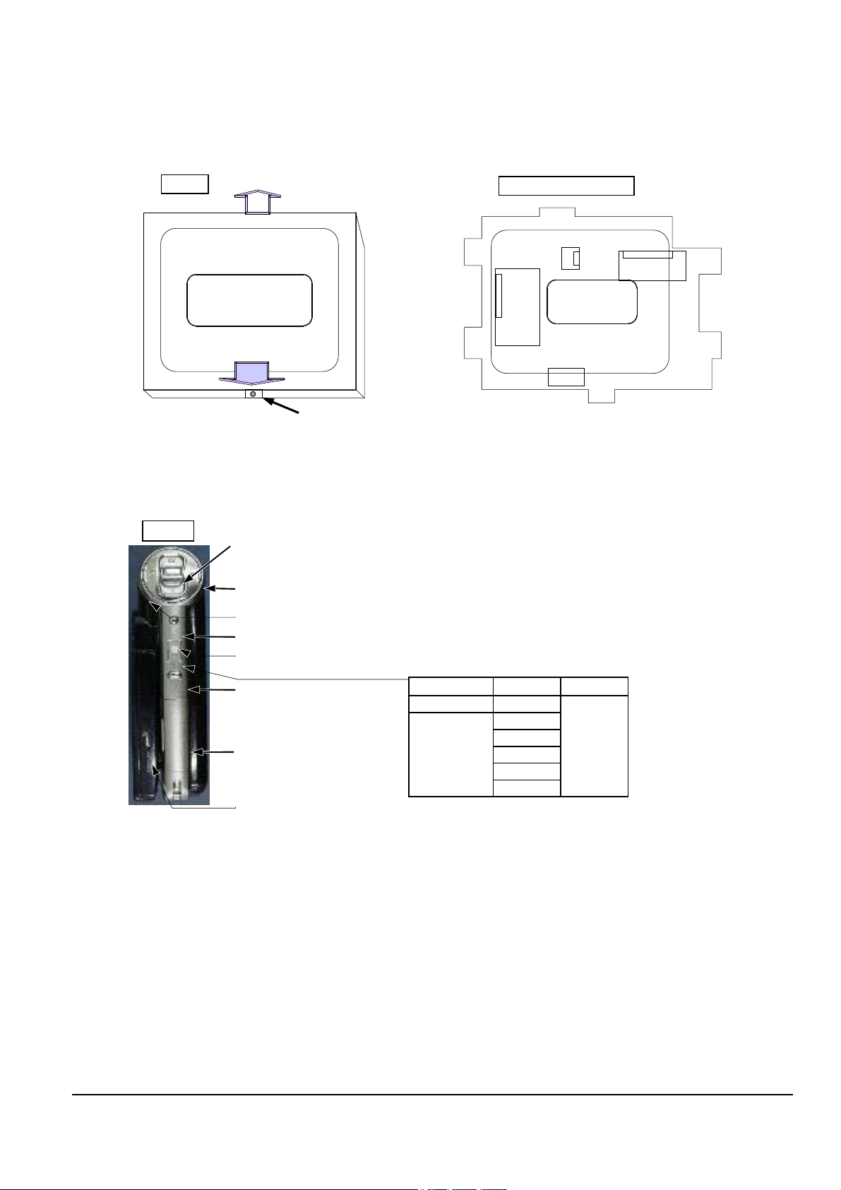
Fig. 13-8 Rear structure
Rear
Zoom Key(VR Type)
Enter Key(Tact Type)
Back Key(Tact Type)
Menu Key(TactType)
REC Key(Tact Type) : both stopped file/AVI file
LED : Power(Green), Charge(Orange)
Memory Stick Slot
Display Key : Assy-LCD(Tact Type)
S/W Position Operation Remark
Off
On
Power Off
Camera
DSC
PC-CAM
MP3
Voice
Recoil Type
Slide-S/W
6) Rear
Page 7
Circuit Operating Description
Samsung Electronics 13-7
Fig. 13-9 TOP structure
Top
Mic
Front
Side
Rear
Side
7) Top
Bottom
Tripod
I/O Connector : 22Pin
Strap ring
Front
Side
Rear
Side
8) Bottom
Fig. 13-10 BOTTOM structure
Page 8

Circuit Operating Description
13-8 Samsung Electronics
13-3 System flow and operation
13-3-1 Usage and technology
1) Function
SPIDER-X, VP-X105 functions in 7 ways.
(1) Digital Camcorder :
Records and Replays AVI files ( after conversion from/to MPEG 4 format) into NAND FLASH Memory
and Memory Stick Pro.
(2) DSC :
Records stationary images of VGA size. Replays the stored scene in a variety of format sizes.
(3) MP3 Player :
Replays MP3 files from internal or external Memory.
(4) Storage :
Stores data into Flash Memory . File management function is supported. Through USB 1.1, data can be
uploaded or downloaded from a PC. Data can be stored using the external Memory Stick.
(5) Voice Recorder :
Records and replays sound.
(6) PC Camera :
Using USB 1.1, it can be used as a PC camera.
(7) Line In / External Camera :
Using this function, it can be connected to external inputs. (Line in / Sports Camera)
Page 9
Circuit Operating Description
Samsung Electronics 13-9
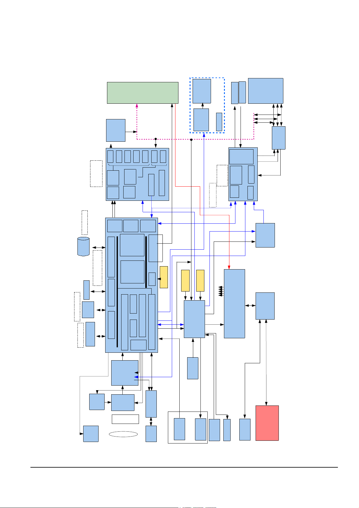
13-3-2 Block Diagram
1) Total Block Diagram
6th Camera DSP
S5C7376X
TG
Camera Process
DIS ZOOM
ARM
JPEG ENC/DEC
MPEG4
ENC
NAND Interface
ITU
656
I/F
ITU
656
I/F
SDRAM
32MB
NAND
Flash
1GB
Modecon
UPD78F0078Y
Reset
XC6413
ZOOM
Focus
Driver
IRIS
Hall
IR
CU
T
CCD
(680K,
800K)
CDS/AGC/A
DC
V.drv
IRIS/Hall
Circuit
Video
ENC
ITU
656
I/F
Video
DEC
DAC1
ITU
656
I/F
DAC2
DAC3
DAC4
DAC5
ADC1
ADC2
Video
AMP
Cradle
LCD drv
CXA3004R
LCD
EEPROM
Audio
Codec
(ADPCM)
Clock
I2S
I/F
Audio
AMP
Audio PLL
DC/DC Conv.
Key
Matrix
Charge
Block
Battery
Speaker
Earphone/
AV In/Out
JACK
Mic
USB 2.0
I2C
I2S
Serial Interface
656 out
clk 27MHz
V
D
LCD module
OSC
54MHz
x1 or x1/2
Techw ell
new ENC/DEC
TW9920
AUDIO
AK4564
MPEG4
DEC
MS-pro I/F
USB 2.0
Dev.
X’tal
8.38MHz
X’tal
32.768KHz
MS-pro
AV in/out
Power
Memory I/F
Audio
I/F
PLL
LEDs
Audio CLK
Serial
Interface
NOR
Flash
128KB
Serial Interface
BACK UP
Battery
STROBO
Circuit
Earphone
out
Audio
Input
Video in/out
BEEP
ML2201
BEEP_nCS, BEEP_DATA, BEEP_PWDN
BEEP_CLK(4.19MHz)
K9K8G08UOM
MB39A108
NJM2561
SST39VF200BGA
K4S283233F
EIS
BLOCK
LEFT ASSY
SWITCHIN
G
BLOCK
Line In
Audio
out
Audio/
Ear-L
Audio-R
Audio-L/
Video In/out
Ex-cam-in
Ex-cam-control
External
Camera In
External
camera
control
Fig. 13-11 Block Diagram
Page 10

Circuit Operating Description
13-10 Samsung Electronics
2) Clock & Reset operation
VCC-CAM3V
SHP,SHD,CLP1
CLP4,PBLK
CDS_RESET
AMP
IRIS_CTL
LENS(X10)
CCD
ICX280
/281
CCD_15V
CCD_7.5V
V1~V4,Vsub
H1,H2,RG
IQ
V-DRIVE
KS7221D
M-DRV IC
UPD16877
FA,FB,ZA,ZB
XV1~XV4,XSG1~2,XSUB
CCD_15V
CCD_-7.5V
IN1~4,EN1~2
VCC_CAM3V
VCC_CAM5V
LEDPSB,F-LED,Z-LED,
FSEN,ZSEN
JTAG
VCC_MS3V
BS
MS_DATAO
MS_CLK
INS
SCK
MSD[0:3]
MEMORY
STICK
SOCKET
EEPROM
AT24C16N
-10SC
HO,HI,DA,DR,MIRIS_CLOSE
VEE_DSP3V
DSP_SDI,DSP_SDO,DSP_CLK,CPU_R/nB,
DSP_nCS
DSP_RESET
CDS/AGE/ADC
TLV990B
DR-
CS, SO
SCK
ADCLK
D0~D9
CCD IN
VSTANDBY
VCC_MODE3V
HALL_AD
MICOM
uPD78F0078Y
MAX1797
STROBO
LED
LED Ctrl.
KEY INPUT
MICOM JIG
FLASH_SI/
SO/SCK
BACKUP
BATTERY
nHD_RST
RESET IC
MAX811
VSTANDBY
nRESET
UNREG_B+
Crystal
32.768KHz
Crystal
8.19MHz
VCC_C0RE1.8V
VCC_PLL1.8V
VCC_DSP3V
CDS_nCS,
CDS_SO, SPICLK1
CDS_CLK
CCD [0:9]
HALL_GAIN
HALL_REF
JTDO, JTMS, JTRST,
JTDI, JTCK
MS_BS
MS_DATA0~3
MS_CLK
MS_DET
EEP_DATA/
EEP_WP
XA[0:25]
XD[0:31]
NOR_nWE, NOR_nCE, NOR_nWP
NOR_nOE, WORD/BYTE
CLE,ALE,NAND_nCE, NAND_nRE,
NAND_nWE, NAND_nWP, NAND_PRE
IO[0:7]
ENC_nRESET
YC_O[0:7]
USB DP/DM
UART/RX,TX
OSCILLATOR
54MHz
27MHz
OUT
SCKE,SnCS,
SnRAS,SnCAS,SnWE
XA[10;21],XA[23;24]
SDQM[0:3]
XD[0;31]
XD[0:14],D15/A
AX[0:19]
NOR_RD/nBY
NOR_nRESET
NAND_RD/nBY
IO[0:7]
VCC_DRAM3V
SDRAM_OIK
AO~A11,BA1~BA0
DQ0~DQ31
DQ0~DQ15
DQ15/A_1(Word)
A0~A19
VCC_NOR3V
VCC_NAND3V
NANDFLASH
(256MB)
K9F2G08U0M
IO0~IO7
EN_VD,EN_HD,LCD_DATA,EEP_CLE,LCD_CS
I2C
VCC_ENC3V
SDA/SCL
ENC_CLK
MP0~MP7
SAA7128
ENCODER
LLC1
S-Y
S-C
C-VIDEO
27MHz
AUDIO PLL
MK2703
VCC_DSE3V
SCLK
LRCK
AUDI_DATA_OUT
AUDI_DATA_IN
AUDIO_PDN
AUDIO_MUTE
CSN,CDTI,CCLE
ST/P1/
PDWN
VOICE IC
ML2201
VCC_AUD3V
PWR_EN,VSD_EN,VSU_EN,12V_DD-ON,15V_DD_ON,
8.19MHz
CAM_DD_ON,BACKLIGHT_ON,MS_ON,
LCD_VDD_ON,VIDEO_EN
nINCG,BATT_INFO,BATT_SENS,DV_IN,nBATT_FAULT
EAR_DET
PI-DET,C_DET
DC/DC BLOK
Power souce
UNREG_B+ VSTANDBY
VDD_****3V, VCC_****5V,
VCC_****1.8V,VCC_BL15V
LCD_12V,CCD_15V,-7.5V
DOCK_DC
CHARGE
BLOCK
POWER
Select
24PIN
IO Conn
VBATTERY
BATTERY
PI_JIG
DCJACK
CRADLE
USB JACK
HP/AV
JACK
Switching
VCC_VID5V
C-VIDEO
S-Y/S-C
C-VIDEO
USB_5V
A/V JACK
A/V
SDRAM 32MB
K4M563233D
-EE80
NOR FLASH 2MB
K8D1616UBM-TI07
I2C
VCC_LCD3V
SDA/
SCL
EEPROM
KS24C020(LCD Only)
EN_R/EN_G/EN_B
SCK
SDAT
HD,VD
VCC_LCD3V
VCC_LCD12V
LCD CONTROLER
CXM3004R
Y/Cr/Cb
2
-
L
C
D
BACK
LIGHT
VCC_BL15V
MIC_CELL
Earphone
SPK
S-Y/S-C
C-VIDEO
VCC_VID5V
VIDEO AMP
BA7660Fs
Crystal
27Mhz
MCLK
12.288MHz
SPEAKER
LINE_out
INT_MIC
Headphone
VCC_AUD3V
VCC_AUD5V
BEEP-IN
AUDIO CODEC
AK4564VQ
SP0, SP1
AUDIO_R, AUDIO_L
ENC_DATA[0:7]
Fig. 13-12 Clock & Reset operation
Page 11

Circuit Operating Description
Samsung Electronics 13-11
3) Total Connection
connect
ESE18LJ02
(LCD MIRROR)
(DETECTOR S/W,SMD)
α,D5-PJ
(3409-001145)¥14.36
M:7745
LENS ASS'Y
CCD B'D
CNC01
1 nNT/PAL
2 XV4
3 XSG2
4 XV3
5 XV1
6 XSG1
7 XV2
8 GND
9H1
10 H2
11 RG
12 GND
13 CCD_OUT
14 GND
15 CCD15V
16 XSUB
17 CCD-7.5V
18 GND
FOCUS_SENS 2
IG_DR- 4
HALL_IN+ 6
HALL_IN- 8
NC 10
ZOOM_A- 12
ZOOM_A+ 14
ZOOM_SENS 16
FOPCUS_B- 18
FOCUS_B+ 20
CNP01
CDS Block
CNZ01
Z/F Block
CNM01
AV-IN/OUT, EAR-OUT
HD-JACK
DSP Block
CN901
DC/DC Block
CNM02
DSP Block
CNE01
Encorder Block
CNL01
CNL03
CNL02
CN501
MICOM Block
1. FOCUS_LED
2. FOCUS_SENS
3. FOCUS_VCC
4. IG_DR-
5. IG_DR+
6. HALL_IN+
7. HALL_OUT+
8. HALL_IN-
9. HALL_OUT-
10. N.C
11. ZOOM_B-
12. ZOOM_A-
13. ZOOM_B+
14. ZOOM_A+
15. ZOOM_LED
16. ZOOM_SENS
17. ZOOM_VCC
18. FOCUS_B-
19. FOCUS_A-
20. FOCUS_B+
21. FOCUS_A+
nNT/PAL 1
XV4 2
XSG2 3
XV3 4
XV1 5
XSG1 6
XV2 7
GND 8
H1 9
H2 10
RG 11
GND 12
CCD_OUT 13
GND 14
CCD15V 15
XSUB 16
CCD-7.5V 17
GND 18
15V
-7.5V
3.0V
3.8V
52892-1890(MACRO:7234)
(1R FPC-CONN.-ZIP EASY 0.5mm BC)
3708-001292(D5-PJ )
1FOCUS_LED
3FOCUS_VCC
5IG_DR+
7 HALL_OUT+
9 HALL_OUT-
11 ZOOM_B-
13 ZOOM_B+
15 ZOOM_LED
17 ZOOM_VCC
19 FOCUS_A-
21 FOCUS_A+
54809-2147(MACRO:?)
(2R FPC-CONN.-ZIP EASY 0.3mm/H1.3 BC)
?( -Molex)
SKRKAAE010
(RESET)
(TACT S/W,SMD)
α,DP-PJ (ALPS)
(3404-001200) ¥14.8
M:7514
15V
-7.5V
52745-1890(MACRO:7784)
(1R FPC-CONN.-ZIP 0.5mm TC)
3708-001215(D5-PJ )
1 MS_BS
2 MS_DATA1
3 MS_DATA0
4 MS_DATA2
5 MS_INS
6 MS_DATA3
7 MS_CLK
8 VCC_MS3V
9 STROBO_B+
10 STROBO_B-
11 AD3_SW_LEFT
12 GND
54548-1290(MACRO:?)
(1R FPC-CONN.-ZIP EASY 0.3mm/H1.3 BC)
?( -Molex)
3.0V
1 VCC(3V)
2JTAG_Reset_n(RESET)
3JTAG_DATA_IN
4JTAG_tms(MODE_SEL)
5JTAG_CLK
6 GND
7JTAG_DATA_OUT
8 nSRST
54550-0890(MACRO:?)
(1R FPC-CONN.-ZIP 0.5mm TC)
?(- )
SW_MIRROR 1
GND 2
ENC_VD 3
ENC_HD 4
GND 5
ENC_G/Y_OUT 6
ENC_R/V_OUT 7
ENC_B/U__OUT 8
GND 9
LCD_DATA 10
EEP_CLK 11
LCD_nCS 12
GND 13
VCC_LCD3V 14
VCC_LCD12V 15
VCC_BL15V 16
SW_DISPLAY 17
GND 18
GND 19
GND 20
54550-2090(MACRO:7495)
(1R FPC-CONN.-ZIP 0.5mm TC)
3708-001675(Gadget- )
3.0V
12V
15V
N.C(BATTERY ID) 1
CRADLE DETECT 2
FLASH_SI 3
ADAPTOR+(5V) 4
ADAPTOR+(5V) 5
PI DET 6
CRADLE_AV_DETECT 7
FLASH_SO 8
FLASH_SCK 9
USB_DM 10
FLASH_CLK 11
GND 12
UART_RX 13
UART_TX 14
USB_DP 15
USB_5V 16
CRADLE_S-C 17
CRADLE_S-Y 18
GND 19
CRADLE_VIDEO 20
N.C 21
FLASH_VPP 22
CRADLE_AUDIO-L 23
CRADLE_AUDIO-R 24
?(MACRO:?)
(?)
?( )
5.0V
5.0V
1 SW_MIRROR
2 GND
3ENC_VD
4ENC_HD
5 GND
6ENC_G/Y_OUT
7ENC_R/V_OUT
8ENC_B/U__OUT
9 GND
10 LCD_DATA
11 EEP_CLK
12 LCD_nCS
13 GND
14 VCC_LCD3V
15 VCC_LCD12V
16 VCC_BL15V
17 SW_DISPLAY
18 GND
19 GND
20 GND
20FLH-SM1-TB(MACRO:7775)
(1R FPC-CONN.-ZIP 0.5mm TC)
?( )
3.0V
12V
15V
TESTER 1
RGT 2
BLUE 3
RED 4
GREEN 5
PSIG 6
HCK1 7
HCK2 8
CEXT/REXT 9
TEST 10
REF 11
HST 12
WIDE 13
SLVSG 14
VSSG 15
VDDG 16
VSS 17
VDD 18
DWN 19
EN 20
VCK 21
VST 22
COM 23
TESTL 24
24FLH-RSM1-TB(MACRO:7776)
(1R FPC-CONN.-ZIP 0.5mm BC)
3708-001647( )
SKQGAF(MACRO:7308)
TACT-SW
3404-000119( )
12V
15V
GND 1
VCC_MODE3V 2
AD5_SW_ZOOM 3
AD4_SW_REAR 4
VSTANDBY(LED B+) 5
LED_POWER 6
LED_CHARG 7
SW_POWER_ON/OFF 8
SW_MODE 9
GND 10
54550-1090(MACRO:?)
(1R FPC-CONN.-ZIP0.5mm TC)
?(?)
3.0V
1N.C(BATTERY ID)
2 CRADLE DETECT
3 FLASH_SI
4 ADAPTOR+(5V)
5 ADAPTOR+(5V)
6PI DET
7 CRADLE_AV_DETECT
8 FLASH_SO
9 FLASH_SCK
10 USB_DM
11 FLASH_CLK
12 GND
13 UART_RX
14 UART_TX
15 USB_DP
16 USB_5V
17 CRADLE_S-C
18 CRADLE_S-Y
19 GND
20 CRADLE_VIDEO
21 N.C
22 FLASH_VPP
23 CRADLE_AUDIO-L
24 CRADLE_AUDIO-R
5.0V
5.0V
1MIC_L
2 GND
3MIC_R
4 GND
SM04B-SSR-H-TB(MACRO:7540)
(CONNECTOR-HEADER 1mm H=1.95 ANGLE)
3711-005090( )
1 SPK+
2 SPK-
SM02B-SURS-TF(MACRO:7770)
(1R CONN.WAFER 0.8mm)
3711-005365 ( Gadget-JST)
1BATTERY +
2BATT_INF
3BATT_DET
4BATTERY -
SM04B-SSR-H-TB(MACRO:7540)
(CONNECTOR-HEADER 1mm H=1.95 ANGLE)
3711-005090( )
CNA01
Audio Block
CNA01
Audio Block
CN902
DC/DC Block
! MS_VSS
@ MS_BS
# MS_VCC
$ MS_DATA1(SDIO)
% MS_DATA2(Reserved)
^ MS_INS
& MS_DATA3(Reserved)
* MS_SCLK
( MS_VCC
) MS_VSS
32MB
SONY
!
)
LEFT-FRONT FPC ASS'Y
A/V-JACK DC-JACK
5.0V
5.0V
CRADLE
MAIN Block
LCD ASS'Y
REAR ASS'Y
DISPLAY
MENUBACKRECEnter/Easy
VOL_UP
HOLD
VOL_DOWN
LCD-DET
N
LCD FPC ASS'Y
MENU
PC GND 5
ID(NC) 4
D+ 3
D- 2
USB B+ 1
connect
with PC
! Power Off
@ Power On- (1) Camera
(2) DSC
(3) PC-CAM
(4) MP3
(5) Voice
B_LED_15V 1
B_LED_FB(GND) 2
SM02B-SURS-TF(MACRO:7770)
(1R CONN.WAFER 0.8mm)
3711-005365( )
Harness13ø
Harness
L
R
MIC-CELL
BATTERY-TEMINAL
Fig. 13-13 Total Wiring Diagram
Page 12

Circuit Operating Description
13-12 Samsung Electronics
13-3-3 Handling the signal
13-3-3 a) Record
In the EE mode, files passed through the lens are transferred into the electronic signal in CCD such as a diagram
below. They are sampled in the CDS/AGC/AD IC and controlled and then transferred in the 10bit Digital
signal and stored Camera process in DSP.Through many steps of process, AVI files processed with the
brightness and color are transmitted by the signal BT.656 Format as a ENCODER/DECODER. And in the
ENCODER BLOCK, they are made into Composite Video Signal or YC or Separate Video Signal and displays at
TV or LCD. Audio data stored through MIC is stored into a MIC input pin of AUDIO DA/AD IC(AK4564) and
outputted into the earphone and LINE out pin as a diagram below.
Fig. 13-14 Camera storage diagram
V.Dri
CCD
CDS/AGC
AD
SDRAM
DRAM
Cont
TG/
SSG
JPEG
ENC
JPEG
DEC
AHB
BUS
DNie
Pre
Process
DIS
Mode
con
AV/
EAR Phone
IN/OUT
CRADLE
LCD
Enc/
Dec
MS Pro
NAND
Flash
Memory
NAND
Cont
Ms
Cont
ITU.R-
656
MICOM
I/F
ARM920T
MPEG4
ENC
MPEG4
DEC
Luminance
and
Chrominance
signal Process
Electronic
Zoom
signal
Process
DSP
Page 13

Circuit Operating Description
Samsung Electronics 13-13
1) Camera MPEG
In the EE mode of the camera, if the REC Button is pressed, the Mode con that recognized SPI communication
sends the signal to DSP. DSP which sends the YCrCb signal to MPEG 4 Encoder Block. And it compresses AVI
files by making DRAM as Buffer and stores them in the Nand Flash Memory or external Memory Stick. In this
case, the camera's EE Routine is operated normal.
Audio Data imported from MIC is stored in the pin of AUDIO DA/AD IC(AK4564) and outputted into the
earphone output pin. Unlike the outputted routine, it is transferred in 32 bit(16bit left, 16 bit right) by the set
value among many sampling clock(22.05KHz,44.1kHz) and transmitted to G.711block in Audio block through
IIS communication. They are compressed here(8 bit left and 8 bit right) and being coded such as a AVI file. AVI
files are generated and stored in NAND FLASH memory or external Memory Stick.
Fig. 13-15 Camera input AVI recording block diagram
V.Dri
CCD
CDS/AGC
AD
SDRAM
DRAM
Cont
TG/
SSG
JPEG
ENC
JPEG
DEC
AHB
BUS
DNie
Pre
Process
DIS
Rec
S/W
Mode
con
AV/
EAR Phone
IN/OUT
CRADLE
LCD
Enc/
Dec
MS Pro
NAND
Flash
Memory
NAND
Cont
Ms
Cont
ITU.R-
656
MICOM
I/F
ARM920T
MPEG4
ENC
MPEG4
DEC
Luminance
and
Chrominance
signal Process
Electronic
Zoom
signal
Process
DSP
Page 14

Circuit Operating Description
13-14 Samsung Electronics
2) Camera JPEG
When the mode of the set is the stopped scene mode, it operates by pressing the REC button. Before operation,
EE status of camera is the same as the AVI recording mode.
If the REC button is pressed, DSP which recognizes that the REC button is pressed communication with the
Mode con transfer the setting of TG block into the stopped scene mode.
After storing images in CCD, generate Meca shutter Close signal and close IRIS quickly.
Through 2 fields, it reads ODD line on 1 field and EVEN line on 2 field and sends the signal.
And it makes a FRAME image and compresses it on JPEG Encoder block using the way of image compression.
Compressed signal is stored to the media(NAND FLASH or MEMORY STICK).
Selected signal is the same as a diagram below.
Fig. 13-16 Camera input JPEG storage Flow Block diagram
V.Dri
CCD
CDS/AGC
AD
SDRAM
DRAM
Cont
TG/
SSG
JPEG
ENC
JPEG
DEC
AHB
BUS
DNie
Pre
Process
DIS
Rec
S/W
Mode
con
AV/
EAR Phone
IN/OUT
CRADLE
LCD
Enc/
Dec
MS Pro
NAND
Flash
Memory
NAND
Cont
Ms
Cont
ITU.R-
656
MICOM
I/F
ARM920T
MPEG4
ENC
MPEG4
DEC
Luminance
and
Chrominance
signal Process
Electronic
Zoom
signal
Process
DSP
Page 15

Circuit Operating Description
Samsung Electronics 13-15
JPEG encoding Timming is as following.
Fig. 13-17 JPEG encoding Timming
odd
even even even
even even
odd
odd
odd
odd
P0
P1
P2
P3 P4
Pn
Pn + 1
Pn + 2 Pn + 3
Input
Source
JPEG
Encode on
JPEG
Capture
JPEG capture
Done
JPEG
Encodeing
JPEG
Encode done
SDRAM
Operation
Normal Operation
Normal Operation
Write only NO Operation
Capture in the
process of
capture
JPEG Capture
done
JPEG Encoding
Capture in the
process of
caoture
Page 16

Circuit Operating Description
13-16 Samsung Electronics
3) Voice
Audio Data imported through MIC is entered into MIC input pin of AUDIO DA/AD IC(AK4564) and
transferred into 32 bit (16 bit left, 16 bit right) digital by the set value among many sampling sampling
clock(22.05k,44.1k etc.) unlike the Routine outputted in earphone output pin by IIS communication. And it is
transmitted into G.711 block of DSP and compressed (8 bit left, 8bit right) by coding as a wav file and stored it in
NAND FLASH memory or external Memory Stick.
* wav file : MS company and IBM company made the sound file. In window, it is used basically to record the
sound. It records the analog audio and digitalizes it like a recorder. It is divided into 22.05KHZ and 44.1KHZ
depending on digitalizing details and is possible to compress stereo and mono.
Fig. 13-18 Voice recording Flow Block diagram
__
BEEP
SPK
HP
LINE OUT1
MIC
LINE IN 1
MS
Stick
PRO
SPK-AMP
HP-AMP
LINE OUT-AMP
MIX/ALC2
DAC
AK4564
L
L
R
R
TW9920
AUDIO
BLOCK
MCLK
LRCK
SCLK
AUDIO
12S
I/F
AUDIO
12S
I/F
ALC1
EQ/
HPF/LPF
ADC
PRE-AMP
MS
STICK
I/F
BRIDGE
S5C7376
SDRAM
NAND
FLASH
DMA
MEMORY I/F
NAND CONT
ARM920T
G.711
G.711
G.726
ENC
G.726
DEC
A
P
B
I
/
F
APB
4
4
8
8
8
16
16
16
16
16
AHB
Page 17

Circuit Operating Description
Samsung Electronics 13-17
4) LINE In / External Camera
Line in/External Camera Record transfers the Analog image data which has been inputted through
AV/Earphone jack to ITU.T-656 File format by a Decoder in external Enc/Dec IC, then to ITU.T-656 Block in
DSP. The Inputted image data is compressed in MPEG4 Encoding Block and combined with compressed
AUDIO file in DSP, then stored as .AVI file in internal NAND Flash Memory or external Memory Stick. The 656
Data entered DSP6 is transmitted to ENC/DEC IC through the external port at ITU.T-656 Block and is made into
YcrCb Signal and displays at LCD.
Fig. 13-19 Line in record Flow Block diagram
V.Dri
CCD
CDS/AGC
AD
SDRAM
DRAM
Cont
TG/
SSG
JPEG
ENC
JPEG
DEC
AHB
BUS
DNie
Pre
Process
DIS
Rec
S/W
Mode
con
AV/
EAR Phone
IN/OUT
CRADLE
LCD
Enc/
Dec
MS Pro
NAND
Flash
Memory
NAND
Cont
Ms
Cont
ITU.R-
656
MICOM
I/F
ARM920T
MPEG4
ENC
MPEG4
DEC
Luminance
and
Chrominance
signal Process
Electronic
Zoom
signal
Process
DSP
Page 18

Circuit Operating Description
13-18 Samsung Electronics
Audio Data inputted through AV/Earphone jack has two types of output routines. One is the general line input
stored through stereo. It is stored into a Line input 1 pin of AUDIO DA/AD IC (AK4564) and outputs into the
speaker. The other is converted to 32bit (16bit of each right/left ) digital signal by the set value among various
sampling clocks (22.05k, 44.1k, etc...) and IIS communication transfers it to G.711 block in the Audio block of
DSP. In the G.711 block, it is compressed (8 bit of each right/left ) ,coded, and combined with compressed image
file. Then it is made into .AVI file, and stored into NAND FLASH memory or external Memory Stick.
External Camera input has two types of output routines. One, which is mono signal, is stored through Audio R
line and stored into L side of a Line input 2 pin of AUDIO DA/AD IC(AK4564) and outputs into the speaker.
The other is converted to 32bit (16bit of each right/left ) digital signal by the set value among various sampling
clocks (22.05k, 44.1k, etc...) and IIS communication transfers it to G.711 block in the Audio block of DSP. In the
G.711 block, it is compressed ( 8 bit of each right/left ) ,coded, and combined with compressed image file. Then
it is made into .AVI file, and stored into NAND FLASH memory or external Memory Stick.
At this time, the signal inputted through Audio L line is used as a communication device to inform REC/STOP
mode of the external camera. It is connected to input port of mode con, so that transfers VD Pulse on the Audio
L line to SET when the external camera input is selected. Then the external camera synchronizes the Rising Edge
of VD Pulse and informs the situation of REC/STOP to mode con.
Fig. 13-20 Line in record Flow Block diagram
__
BEEP
SPK
HP
LINE OUT1
MIC
LINE IN 2
MS
Stick
PRO
SPK-AMP
HP-AMP
LINE OUT-AMP
MIX/ALC2
DAC
AK4564
L
L
R
R
TW9920
AUDIO
BLOCK
MCLK
LRCK
SCLK
AUDIO
12S
I/F
AUDIO
12S
I/F
ALC1
EQ/
HPF/LPF
ADC
PRE-AMP
MS
STICK
I/F
BRIDGE
S5C7376
SDRAM
NAND
FLASH
DMA
MEMORY I/F
NAND CONT
ARM920T
G.711
G.711
G.726
ENC
G.726
DEC
A
P
B
I
/
F
APB
4
4
8
8
8
16
16
16
16
16
AHB
Page 19

Circuit Operating Description
Samsung Electronics 13-19
13-3-3 b) Replay
1) MPEG
It replays by reading and extending AVI files compressed and stored in NAND Flash memory or external
memory and by decoding MPEG4 files and images and audio data compressed as G.711 and by transmitting
them to TV, LCD, speaker, earphone.
First, it reads AVI files stored in the Memory Stick or NAND Flash memory.
Then, it decodes AVI files and separates MPEG4 files and images and audio data compressed as G.711. And it
decodes image data in MPEG4 Decoder block and through ITU.R 656 block, it is sent to ncoder/Decoder Both
IC(Techwell IC). In Encoder Block of IC, it is transferred as Composite Video signal for TV and YCrCb signal for
LCD and displays. Audio signal is decoded in G.711 block and sent to AK4564 IC through IIS communication In
AK4564, it converts D/A and outputted through speaker, earphone/AV, Cradle.
Fig. 13-21 MPEG replay Flow Block diagram
V.Dri
CCD
SDRAM
DRAM
Cont
TG/
SSG
JPEG
ENC
JPEG
DEC
AHB
BUS
DNie
Pre
Process
DIS
Rec
S/W
Mode
con
AV/
EAR Phone
IN/OUT
CRADLE
LCD
Enc/
Dec
MS Pro
NAND
Flash
Memory
NAND
Cont
Ms
Cont
ITU.R-
656
MICOM
I/F
ARM920T
MPEG4
ENC
MPEG4
DEC
Luminance and
Chrominance
signal Process
Electronic
Zoom signal
Process
DSP
CDS/AGC
AD
Page 20

Circuit Operating Description
13-20 Samsung Electronics
Fig. 13-22 MPEG replay A/V handling Flow Block diagram
BEEP
SPK
HP
LINE OUT1
MIC
LINE IN 1
MS
Stick
PRO
SPK-AMP
HP-AMP
LINE OUT-AMP
MIX/ALC2
DAC
AK4564
L
L
R
R
TW9920
AUDIO
BLOCK
MCLK
LRCK
SCLK
AUDIO
12S
I/F
AUDIO
12S
I/F
ALC1
EQ/
HPF/LPF
ADC
PRE-AMP
MS
STICK
I/F
BRIDGE
S5C7376
SDRAM
NAND
FLASH
DMA
MEMORY I/F
NAND CONT
ARM920T
G.711
G.711
G.726
ENC
G.726
DEC
A
P
B
I
/
F
APB
4
4
8
8
8
16
16
16
16
16
AHB
Page 21

Circuit Operating Description
Samsung Electronics 13-21
2) JPEG
It replays the stopped scene by decoding JPEG file stored NAND Flash memory or external memory and
displays at TV and LCD.
First, it reads JPEG files stored in the Memory Stick or NAND Flash memory.
Then, it decodes JPEG files in MPEG4 Decoding block and through ITU.R 656 block, they are sent to
ncoder/Decoder Both IC(Techwell IC). In Encoder Block of IC, it transferred as Composite Video signal for TV
and YCrCb signal for LCD and displays.
Fig. 13-23 JPEG replay Flow Block diagram
V.Dri
CCD
CDS/AGC
AD
SDRAM
DRAM
Cont
TG/
SSG
JPEG
ENC
JPEG
DEC
AHB
BUS
DNie
Pre
Process
DIS
Rec
S/W
Mode
con
AV/
EAR Phone
IN/OUT
CRADLE
LCD
Enc/
Dec
MS Pro
NAND
Flash
Memory
NAND
Cont
Ms
Cont
ITU.R-
656
MICOM
I/F
ARM920T
MPEG4
ENC
MPEG4
DEC
Luminance
and
Chrominance
signal Process
Electronic
Zoom
signal
Process
DSP
Page 22

Circuit Operating Description
13-22 Samsung Electronics
3) MP3
For replaying MP3 files, it reads MP3 files stored NAND Flash memory or external memory and writes SDRAM.
Then, it decodes MP3 files in ARM920 as SW. Decoded data is sent to into AK4564 IC through IIS interface and
AK4564 converts DA and outputted to speaker and earphone.
Fig. 13-24 MP3 replay Flow Block diagram
__
BEEP
SPK
HP
LINE OUT1
MIC
LINE IN 1
MS
Stick
PRO
SPK-AMP
HP-AMP
LINE OUT-AMP
MIX/ALC2
DAC
AK4564
L
L
R
R
TW9920
AUDIO
BLOCK
MCLK
LRCK
SCLK
AUDIO
12S
I/F
AUDIO
12S
I/F
ALC1
EQ/
HPF/LPF
ADC
PRE-AMP
MS
STICK
I/F
BRIDGE
S5C7376
SDRAM
NAND
FLASH
DMA
MEMORY I/F
NAND CONT
ARM920T
G.711
G.711
G.726
ENC
G.726
DEC
A
P
B
I
/
F
APB
4
4
8
8
8
16
16
16
16
16
AHB
Page 23

Circuit Operating Description
Samsung Electronics 13-23
4) Voice
It replays by reading and extending WAV files compressed and stored in NAND Flash memory or external
memory and by decoding Voice data files compressed as G.711 and by transmitting them to TV, LCD, speaker,
earphone.
First, it reads .WAV files stored in the Memory Stick or NAND Flash memory.
Then, it decodes .WAV files and separates Voice data files compressed as G.711. And it decodes image data in
G.711block and through IIS communication, it is sent to AK4564 IC and converts D/A in AK4564 and outputted
through speaker, earphone/AV output, Cradle.
Fig. 13-25 Voice replay Flow Block diagram
__
BEEP
SPK
HP
LINE OUT1
MIC
LINE IN 1
MS
Stick
PRO
SPK-AMP
HP-AMP
LINE OUT-AMP
MIX/ALC2
DAC
AK4564
L
L
R
R
TW9920
AUDIO
BLOCK
MCLK
LRCK
SCLK
AUDIO
12S
I/F
AUDIO
12S
I/F
ALC1
EQ/
HPF/LPF
ADC
PRE-AMP
MS
STICK
I/F
BRIDGE
S5C7376
SDRAM
NAND
FLASH
DMA
MEMORY I/F
NAND CONT
ARM920T
G.711
G.711
G.726
ENC
G.726
DEC
A
P
B
I
/
F
APB
4
4
8
8
8
16
16
16
16
16
AHB
Page 24

Video Format Planar YUV 4:2:0 (ie YYYYYYY....UUUU....VVVV)
Video Size 160 x 120 (28800 Byte/Frame)
Frame Rate 30fps(MP:962), 25fps(MP:722), 20fps(MP:578), 15fps(MP:439), 10fps(MP:290)
Circuit Operating Description
13-24 Samsung Electronics
13-3-3 c) USB
1) Streaming
The next is USB Streaming specification.
(1) Computer Environment
PC installed OS, Pixela Video Streaming Driver included USB1.1
(2) Video Streaming
1-1) Format
<Table 13-2 Streaming Format>
(MP:Max Packet Size)
1-2) Descriptor
Use Isochronous for transmitting Video Streaming. It is necessary to set the temporary value at a Device
about Isochronous set with quantity and wMax Packet Size of Interface. bAlternate Setting is necessary
to set 0 about endpoint of 0x00. It is necessary to pass WHQL.
1-3) Transmission Timing
After starting transmitting Video Streaming, the end Timing doesn't recognize from Host using Vendor
Command but performs by cutting Alternate Setting(USB standard Request Set Interface). More specific
method is to set Alternate Setting as 0x00 in the part which application doesn't need image data. That
means it doesn't transmit Video Streaming because Isochronous is set 0. When sending Video
Streaming, it alarms the necessary thing to send Video Streamingto a Device using Set Interface
to proper Index except Alternate Setting from Host. Then, it performs Video Streaming using
Isochronous by Driver.When finishing Video Streaming, it is set Alternate Setting as 0x00.
1-4) Transmission Protocol
Video Streaming uses Isochronous but Data Packet to store Streaming Data sends 2Byte Packet Tag
exactly. This Packet Tag uses missing Packet and the first extracted Frame from Driver.
Packet Tag is set 0x0000 at the front of Video frame and "1" increment value is set up to the final Data
Packet of Video Frame Data (28800 Bytes). Packet Tag transmitted to Packet alarms the final route of
Video Frame as "1" at the step of 15bit which is transmitted to Packet to the Driver. (The next Video
Frame Data doesn't include the final Data Packet and it starts the next Packet.) The next transmission of
Video Frame Data starts the new Packet Tag in 0x0000. And this step continues.
* In case that the Alternate Setting is set to 0x04(wMax Packet Size=0x01b7(439) in Interface Descriptor),
Isochronous Packet is as following.
Page 25

Circuit Operating Description
Samsung Electronics 13-25
Fig. 13-26 Isochronous Packet / Transmission of 1Frame
0x0000
Video Data0
2Byte
437Byte
2Byte
437Byte
2Byte
437Byte
2Byte
437Byte
2Byte
437Byte
0x0001
Video Data1
0x0002
Video Data2
0x0001
Video Data65
0x0040
Video Data64
1Packet
439Byte
1Packet
439Byte
1Packet
439Byte
1Packet
439Byte
1Packet
439Byte
Transmission of 1Frame (Video Total Length : 28800 Byte)
Fig. 13-27 Isochronous Packet / Transmission of 2Frame
0x0000
Video Data0
2Byte
437Byte
2Byte
437Byte
2Byte
437Byte
2Byte
437Byte
2Byte
437Byte
0x0000
Video Data0
0x0000
Video Data0
0x0000
Video Data0
0x0000
Video Data0
1Packet
439Byte
1Packet
439Byte
1Packet
439Byte
1Packet
439Byte
1Packet
439Byte
Transmission of 2Frame (Video Total Length : 28800 Byte)
Page 26

Circuit Operating Description
13-26 Samsung Electronics
(3) Audio Streaming
Use Audio Class of USB standard Class.
Macintoshi doesn't support Sampling Rate 8KHz in OS Level.
To extend the transmission range of Video Streaming, don't set Sampling Rate.
(Sampling Rate : 16KHz Recommendable)
- Audio Streaming uses USB 1.1r as a PC camera function and displays AVI files of 160X120 size to TV in the
speed of 15Frame per a second by transmitting Y,U,V to PC.
If Streaming mode is selected and REC Button is pressed, TG/SSG block of DSP generates Timming to output
160X120 15 frame display. And image from CD is passed through CDS/AGC/AD Block and they are
digitalized into Sampling, Gain control and 10bit and entered in DSP. This signal passes processing part and
is transmitted to PC through USB 1.1controller converted into Y,U,V signal.
Fig. 13-28 USB Streaming Block diagram
V.Dri
CCD
CDS/AGC
AD
SDRAM
DRAM
Cont
TG/
SSG
JPEG
ENC
JPEG
DEC
AHB
BUS
DNie
Pre
Process
DIS
Rec
S/W
Mode
con
PC
CRADLE
LCD
Enc/
Dec
MS Pro
NAND
Flash
Memory
NAND
Cont
Ms
Cont
ITU.R-
656
USB
Cont.
22PIN I/O
MICOM
I/F
ARM920T
MPEG4
ENC
MPEG4
DEC
Luminance
and
Chrominance
signal Process
Electronic
Zoom
signal
Process
Page 27

Circuit Operating Description
Samsung Electronics 13-27
13-3-4 Booting step
13-3-4 a) Operation step
Booting step is as following.
1. ADAPTER IN OR Battery IN
2. EVER Power(VATANDBY) generation
3. MODE con Power input and 8.38MHz crystal launching start
4. HARDWARE RESET generation 8.38MHz crystal launching stop
5. RESET generation within mode con
6. 8.38MHz crystal launching restart
7. mode con initial
8. Enter the mode con sleep mode(Only operating in 8.38MHz stop, 32Khz)
9. Enter POWER ON KEY
10. In sleep mode, enter the normal operation mode (8.38MHz crystal launching restart)
11. DSP_RESET signal generation
12. DSP RESET operating
13. Moves booting program of NOR FLASH MEMORY into SRAM within DSP
14. Moves OS and DRIVER π◊ GUI into NAND FLASH MEMORY by the booting program and moves into
SDRAM and enter the OS mode.
15. Reads the value of REGISTER Setting of NOR FLASH MEMORY and performs REGISTER Setting within
DSP and around IC.
Page 28

Circuit Operating Description
13-28 Samsung Electronics
MEMO
 Loading...