

Samsung S3C9004, S3C9014, S3P9004, S3P9014 Datasheet

S3C9004/P9004/C9014/P9014 PRODUCT OVERVIEW
1 PRODUCT OVERVIEW
SAM87RI PRODUCT FAMILY
Samsung's SAM87RI family of 8-bit single-chip CMOS microcontrollers offers a fast and efficient CPU, a wide
range of integrated peripherals, and various mask-programmable ROM sizes.
A dual address/data bus architecture and a large number of bit- or nibble-configurable I/O ports provide a flexible
programming environment for applications with varied memory and I/O requirements. Timer/counters with
selectable operating modes are included to support real-time operations. Many SAM87RI microcontrollers have
an external interface that provides access to external memory and other peripheral devices.
S3C9004/P9004/C9014/P9014 MICROCONTROLLER
The S3C9004/P9004/C9014/P9014 single-chip 8-bit microcontroller is fabricated using an advanced CMOS
process. It is built around the powerful SAM87RI CPU core.
Stop and Idle power-down modes were implemented to reduce power consumption. To increase on-chip register
space, the size of the internal register file was logically expanded. The S3C9004/P9004/C9014/P9014 has 4 K
bytes of program memory on-chip.
Using the SAM87RI design approach, the following peripherals were integrated with the SAM87RI core:
— Five configurable I/O ports (32 pins)
— 12 bit-programmable pins for external interrupts
— 8-bit timer/counter with three operating modes
The S3C9004/P9004/C9014/P9014 is a versatile microcontroller that can be used in a wide range of general
purpose applications. It is especially suitable for use as a keyboard controller and is available in a 40-pin DIP and
a 44-pin QFP package.
OTP
The S3C9004/C9014 microcontroller is also available in OTP (One Time Programmable) version,
S3P9004/P9014. S3P9004/P9014 microcontroller has an on-chip 8-Kbyte one-time-programmable EPROM
instead of masked ROM. The S3P9004/P9014 is comparable to S3C9004/C9014, both in function and in pin
configuration.
1-1

PRODUCT OVERVIEW S3C9004/P9004/C9014/P9014
FEATURES
CPU
• SAM87RI CPU core
Memory
• 4-Kbyte internal program memory (ROM)
• 208-byte internal register file
• 8-Kbyte external program memory
• 8-Kbyte external data memory
Instruction Set
• 41 instructions
• IDLE and STOP instructions added for powerdown modes
Instruction Execution Time
• 1.5 µs at 4 MHz f
OSC
Interrupts
• 14 interrupt sources with one vector, Each
source has its pending bit
• One level, one vector interrupt structure
General I/O
• Five ports (32 pins total)
• Three bit-programmable ports (20 pins total)
• Two bit-programmable ports with external
interrupts (12 pins total)
Timer/Counter
• One 8-bit basic timer for watchdog function and
programmable oscillation stabilization interval
generation function
• One 8-bit timer/counter with PWM mode
Operating Temperature Range
• – 40°C to + 85°C
Operating Voltage Range
• 4.5 V to 5.5 V for S3C9004/P9004
• 2.7 V to 5.5 V for S3C9014/P9014
Package Types
• 40-pin DIP
Oscillation Circuit Options
• 4 MHz RC oscillator with on chip capacitor for
S3C9004/P9004 ( –10% RC accuracy at VDD ±
5% and Ta = 0°C–70°C, using 1% external
precision resistor)
• RC oscillator for S3C9004/P9004
• Crystal/ceramic oscillator for S3C9014/P9014
1-2

S3C9004/P9004/C9014/P9014 PRODUCT OVERVIEW
BLOCK DIAGRAM
X
X
IN
OUT
RESET
V
DD
V
SS1
MAIN
OSC
Basic
Timer
Timer 0
P0.0-P0.4/A8-A12,
P0.5-P0.7
PORT
INTERRUPT CONTROL
P1.0-P1.7/
AD0-AD7
PORT PORT
SAM87RI BUS
I/O PORT AND
SAM87RI CPU
P2.0-P2.7/INT,
AS, DS
, R/W,
DM
EA (TEST)
V
DD
V
SS1
PORT
PORT
P3.0
P3.1
P3.2
P3.3/CLO
P4.0/INT
P4.1/INT/T0CLK
P4.2/INT
P4.3/INT/T0OUT
4-KB ROM
208-BYTE
REGISTER
FILE
Figure 1-1. Block Diagram
1-3

PRODUCT OVERVIEW S3C9004/P9004/C9014/P9014
PIN ASSIGNMENTS
P3.0
INT/P4.0
T0CLK/INT/P4.1
INT/P4.2
T0OUT/INT/P4.3
/INT/P2.0
AS
/INT/P2.1
DS
R/W/INT/P2.4
/INT/P2.3
DM
INT/P2.4
INT/P2.5
INT/P2.6
INT/P2.7
NC
V
SS1
AD7/P1.7
AD6/P1.6
AD5/P1.5
AD4/P1.4
AD3/P1.3
1
2
3
4
5
6
7
8
9
10
11
12
13
14
15
16
(Top View)
17
18
19
20
40
39
38
37
36
35
34
33
32
31
30
29
S3C9004/P9004
S3C9014/P9014
28
27
26
40-DIP
25
24
23
22
21
P3.1
P3.2
P3.3/CLO
V
DD
P0.0/A8
P0.1/A9
P0.2/A10
P0.3/A11
P0.4/A12
P0.5
P0.6
P0.7
X
OUT
X
IN
RESET
V
SS2
EA
P1.0/AD0
P1.1/AD1
P1.2/AD2
1-4
Figure 1-2. Pin Assignment Diagram (40-Pin DIP Package)
S3C9004/P9004/C9014/P9014 PRODUCT OVERVIEW
PIN DESCRIPTIONS
Table 1-1. S3C9004/P9004/C9014/P9014 Pin Descriptions
Pin
Names
Pin
Type
Pin
Description
P0.0-P0.7 I/O Bit-programmable I/O port for Schmitt trigger
input or open-drain output. Port0 can also be
configured as external interface address lines A8A12.
P1.0-P1.7 I/O Bit-programmable I/O port for Schmitt trigger
input, push-pull, or open-drain output. Port1 can
alternatively be used as external interface
address/data lines AD0-AD7.
P2.0-P2.7 I/O Bit-programmable I/O port for Schmitt trigger
input or push-pull output. Port2 can be
individually configured as external interrupt
inputs. Especially, P2.0-2.3 can be configured for
external bus control signal.
P3.0-P3.3 I/O Same general characteristics as Port1. Port3 are
designed for to drive LED directly. P3.3 can be
used to system clock output (CLO) port.
P4.0-P4.3 I/O Bit-programmable I/O port. Input mode or n-
channel open-drain output mode is software
assignable. Port4 can be individually configured
as external interrupt inputs. Pull-up resistors are
also software assignable. Especially, P4.1 can be
used T0CLK input and P4.3 also T0OUT for
Timer 0.
XIN, X
OUT
– System clock input and output pin (for RC
oscillator, crystal/ceramic oscillator, or external
clock source)
INT I External interrupt for bit-programmable port2 and
port4 pins when set to input mode.
RESET
I
RESET signal input pin. Schmitt trigger input with
internal pull-up resistor.
EA I External Memory Access (EA) pin with 2 modes:
0V = Normal Operation Mode
5V = ROMLESS Operation Mode
(Must be connected to VSS during normal
operation mode)
V
SS1
V
DD
V
,
SS2
– Power input pin – 37 –
– Vss1 is a ground power for CPU core.
Vss2 is a ground power for I/O and OSC block
NC – No connection
(This pin would be better connecting to VSS)
Circuit
Number
Pin
Numbers
C 36-29 A8-A12
C 23-16 AD0-AD7
D 6-13
INT, AS,
DS, R/W,
C 1, 40-38 P3.3/CLO
D 2-5 INT,
T0CLK,
T0OUT
– 27, 28 –
– 2-13 PORT2/
PORT4
A 26 –
B 24 –
– 15, 25 –
– 14 –
Share
Pins
DM
1-5
PRODUCT OVERVIEW S3C9004/P9004/C9014/P9014
PIN CIRCUITS
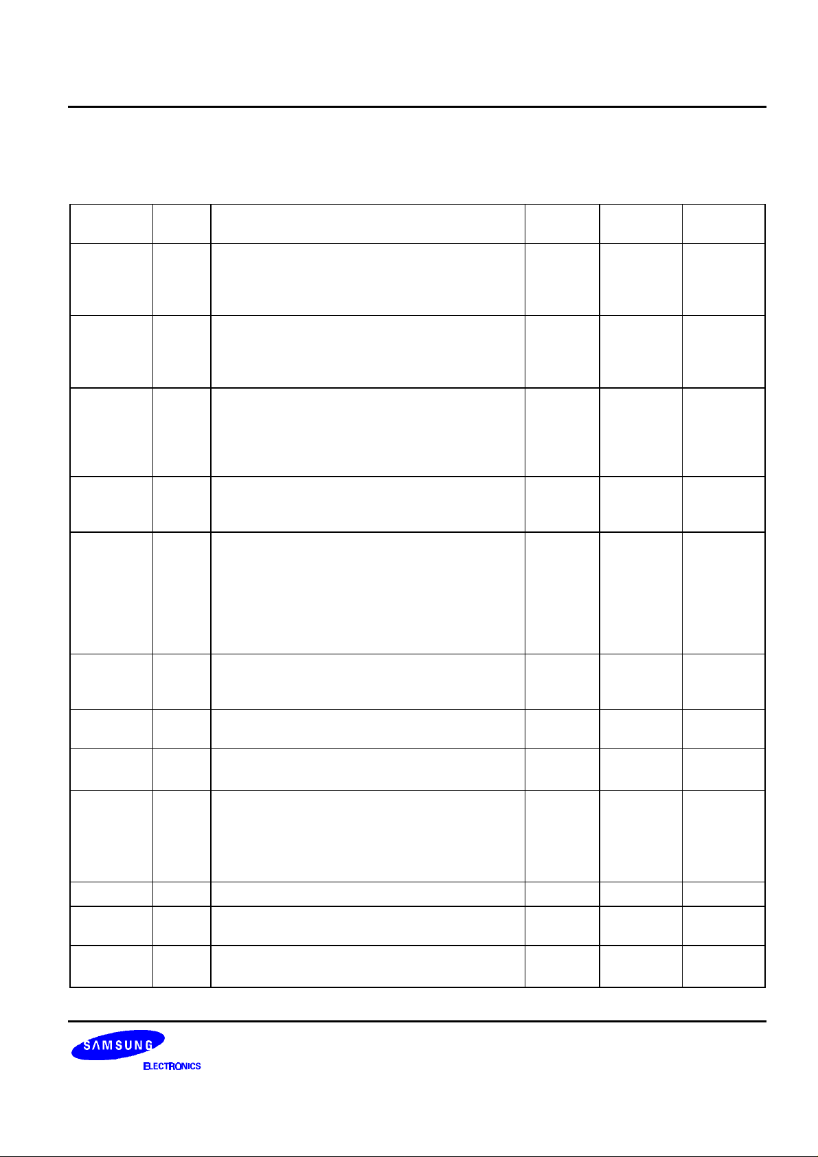
Table 1-2. Pin Circuit Assignments for the S3C9004/P9004/C9014/P9014
Circuit Number Circuit Type S3C9004/P9004/C9014/P9014 Assignments
A I
B I EA input
C I/O Ports 0, 1, and 3
D I/O Ports 2 and 4
VDD
RESET signal input
PULL-UP
RESISTOR
IN
Noise
Filter
Figure 1-3. Pin Circuit Type A (RESETRESET)
OUTPUT
DATA
OPEN
DRAIN
OUTPUT
DISABLE
INPUT
DATA
MUX
D0
D1
IN
0 V = Internal ROM Access
5 V = External ROM Access
Figure 1-4. Pin Circuit Type B (EA)
VDD
I/O
V
SS
1-6
MODE INPUT DATA
OUTPUT
INPUT
D0
D1
Figure 1-5. Pin Circuit Type C (Ports 0, 1, and 3)

S3C9004/P9004/C9014/P9014 PRODUCT OVERVIEW
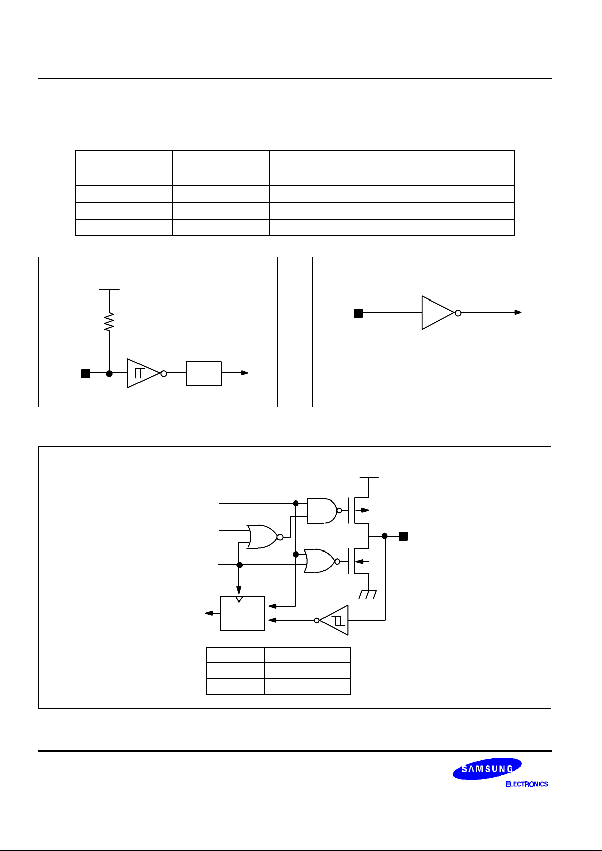
VDD
PULL-UP
RESISTOR
PULL-UP
ENABLE
VDD
OUTPUT
DATA
OPEN
DRAIN
I/O
OUTPUT
DISABLE
V
SS
INPUT
DATA
MUX
D0
D1
MODE INPUT DATA
OUTPUT D0
INPUT
D1
Figure 1-6. Pin Circuit Type D (Ports 2 and 4)
1-7
PRODUCT OVERVIEW S3C9004/P9004/C9014/P9014
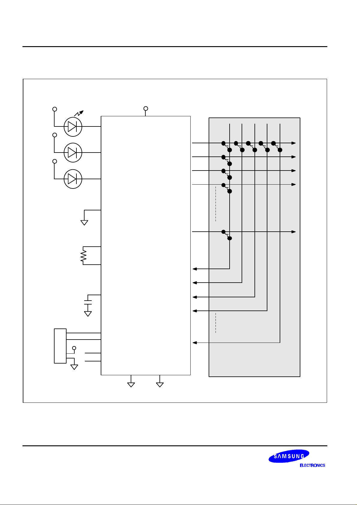
APPLICATION CIRCUIT
5V
5V
V
DD
0
1
PORT 3
PORT 0PORT 1PORT 2
EA
2
3
15
S3C9004
X
IN
R
OSC
X
OUT
S3P9004
0
1
RESET
H
O
S
T
CLK
DATA
PORT 4
V
SS1
V
SS2
2
3
7
KEYBOARD
MATRIX
Figure 1-7. Keyboard Control Application Circuit Diagram
1-8
 Loading...