

Samsung S3C7281 Datasheet

S3C7281 PRODUCT OVERVIEW
1 PRODUCT OVERVIEW
OVERVIEW
The S3C7281 is a SAM48 core-based 4-bit CMOS single-chip microcontroller. It is built around the SAM48 core
CPU and contains ROM, RAM. 14 I/O lines, buzzer and inverted buzzer output, and LCD driver/controller with an
up-to-64-dot.
The S3C7281 can be used for dedicated control functions in a variety of applications, and is especially designed
for LCD general purpose.
1-1
PRODUCT OVERVIEW S3C7281
FEATURES
Memory
• 1024 x 8 bit program memory
• 64 x 4 bit data memory
(Including stack and excluding LCD RAM)
14 I/O Pins
• I/O: 6 pins
• Output: 8 pins(Sharing with segment outputs)
8-Bit Basic Timer
• 4 clock source(0.26, 2.1, 8.2, 32.8ms at 1MHz)
• Watch-dog timer
Watch Timer
• Quasi interrupt(stand by release mode only)
• Time divider:
3.91, 32, 125, 500ms at fw=32.8kHz
• BUZ, BUZ output(0.5, 1, 2, 4kHz at
1MHz<main>, 32.8kHz<sub>)
Key Interrupt input(Quasi-interrupt)
• Falling edge detection(KS0, KS1)
• Stand by mode(idle, stop) release
Power on RESET (Program ROM MASK option)
• Initial power on RESET
• Reset operation under 2.0V
LCD Display
• 16 segments and 4 common pins
• 2, 3, and 4 common selectable
Memory Mapped I/O Structure
• Data memory bank 15
Power-Down Modes
• Idle: only CPU clock stops
• Stop: Main System clock and CPU clock stops
• Subsystem clock stop mode
Oscillation Sources
• Main: Internal RC OSC(1MHz)
• Sub: External 32.8kHz crystal only
Instruction Execution Times
• Main system clocks:4, 8, 64µs at 1MHz
• Subsystem clocks: 122 µs at 32.768 kHz
Operating Voltage Range
• 1.8 V to 5.5 V at 1MHz/32.8kHz
Power Consumption(The LVD circuit needs
100uA or more current on all the below mode)
• Main: Operation - 0.5mA at 1MHz, 3V
• Sub: Operation - 12µA at LCD off, 3V
Idle - 5µA at LCD off idle, 3V
Stop - 1µA at 5.5V
Operating Temperature
• - 40 °C to 85 °C
Package Type
• 32-SOP-450A Package
• Internal resistor for LCD bias(170 KΩ)
1-2
S3C7281 PRODUCT OVERVIEW
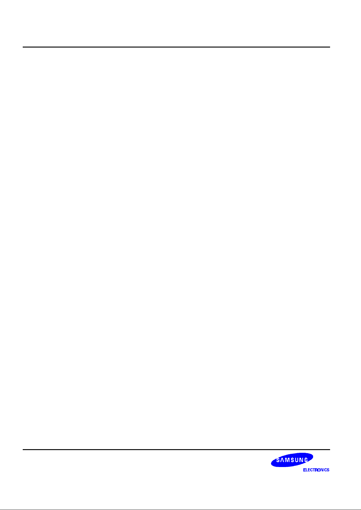
SEG10-SEG17/
BLOCK DIAGRAM
P0.3
P0.2/
BUZ
P0.1/BUZ
P0.0/CLO
P1.1/KS1
P1.0/KS0
P2.4-P2.7/
SEG13-SEG10
P2.0-P2.3/
SEG17-SEG14
I/O Port 0
I/O Port 1
Output Port 2
RESET
XT
Interrupt
Control
Block
Internal
Interrupts
Instruction Decoder
Arithmetic
and
Logic Unit
64 x 4-Bit
Data Memory
XT
IN
Sub Clock
Main Clock
(Internal
RC OSC)
OUT
Instruction
Register
Program
Counter
Program
Status Word
Stack
Pointer
1024-Byte
Program Memory
Basic
Timer
Watch
Timer
LCD
Driver/
Controller
Power on
RESET
* AGP Option
Watchdog
Timer
COM0-COM1
COM2-COM3/
SEG0-SEG1
SEG2-SEG9
P2.7-P2.0
Figure 1-1. S3C7281 Simplified Block Diagram
1-3
PRODUCT OVERVIEW S3C7281
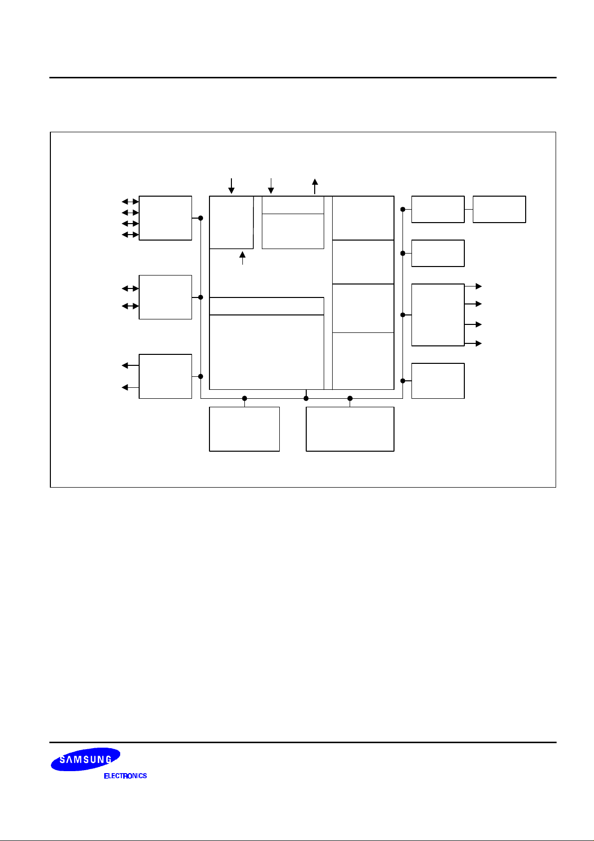
PIN ASSIGNMENTS
VSS
XTIN
XTOUT
TEST
P1.0/KS0
P1.1/KS1
RESET
COM0
COM1
COM2/SEG0
COM3/SEG1
SEG2
SEG3
SEG4
SEG5
SEG6
NOTE: Reserved pins for the OTP version in the future
1
2
3
4
5
6
7
8
9
10
11
12
13
14
15
16
(note)
SCLK
(note)
SDAT
(32-SOP-450A)
S3C7281
32
31
30
29
28
27
26
25
24
23
22
21
20
19
18
17
Figure 1-2. S3C7281 32-SOP Pin Assignment Diagram
VDD
P0.0/CLO
P0.1/BUZ
P0.2/
BUZ
P0.3
P2.0/SEG17
P2.1/SEG16
P2.2/SEG15
P2.3/SEG14
P2.4/SEG13
P2.5/SEG12
P2.6/SEG11
P2.7/SEG10
SEG9
SEG8
SEG7
1-4
S3C7281 PRODUCT OVERVIEW
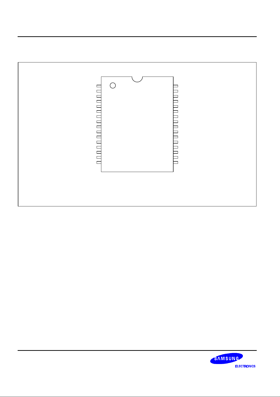
PIN DESCRIPTIONS
Table 1-1. S3C7281 Pin Descriptions
Pin Name Pin Type Description Number Share Pin
P0.0
P0.1
P0.2
P0.3
I/O 4-bit I/O port.
1-bit or 4-bit read/write and test is possible.
1-bit unit pull-up resistors are assignable to input pins
by software and are automatically disabled for output
31
30
29
28
CLO
BUZ
BUZ
pins. Individual pins can be allocated as input or
output(1-bit unit). The n-channel open-drain or pushpull output can be selected by software(1-bit unit).
P1.0
P1.1
I/O 4-bit I/O port.
1-bit or 4-bit write and test is possible.
5
6
KS0
KS1
4-bit unit pull-up resistors are assignable to input pins
by software and are automatically disabled for output
pins. The pins can be allocated as input or output(4-bit
unit). The n-channel open-drain or push-pull output
can be selected by software(4-bit unit).
P2.0 - P2.7 O 8-bit output port.
1-bit, 4-bit, 8-bit read/write and test is possible.
27 - 20 SEG17-
SEG10
The n-channel open-drain or push-pull output can be
selected by software(4-bit unit).
CLO I/O Clock output. 31 P0.0
BUZ I/O Buzzer signal output. 30 P0.1
BUZ
KS0
KS1
SEG0
SEG1
I/O Inverted buzzer signal output. 29 P0.2
I/O External interrupt with falling edge detection. 5
6
O LCD segment signal output. 10
11
P1.0
P1.1
COM0
COM1
SEG2-SEG9 O LCD segment signal output. 12 - 19 –
SEG10-SEG17 O LCD segment signal output. 20 - 27 P2.7 - P2.0
COM0
COM1
COM2
COM3
XT
IN
XT
OUT
V
DD
V
SS
RESET
TEST I
O LCD common signal output. 8
9
O LCD common signal output. 10
11
SEG0
SEG1
– Crystal oscillator pins for subsystem clock. 2
3
– Main power supply. 32 –
– Ground. 1 –
I Chip reset signal input. 7 –
Chip test signal input (must be connected to VSS).
4 –
–
–
1-5

PRODUCT OVERVIEW S3C7281
Table 1-1. S3C7281 Pin Descriptions (Continued)
Pin Name Pin Type Share Pin Circuit Type RESET Value
P0.0 - P0.2
I/O CLO, BUZ, BUZ E-2 Input
P0.3
P1.0 - P1.1 I/O KS0, KS1 E-2 Input
P2.0 - P2.7 O SEG17 - SEG10 H-28 Low output
COM0, COM1 O – H-4 Low output
COM2, COM3 O SEG0, SEG1 H-6 Low output
SEG2 - SEG9 O – H-5 Low output
SEG10 - SEG17 O P2.7 - P2.1 H-28 Low output
V
DD
V
SS
RESET
XTIN, XT
OUT
– – – –
– – – –
I – B –
– – – –
TEST I – – –
1-6
S3C7281 PRODUCT OVERVIEW
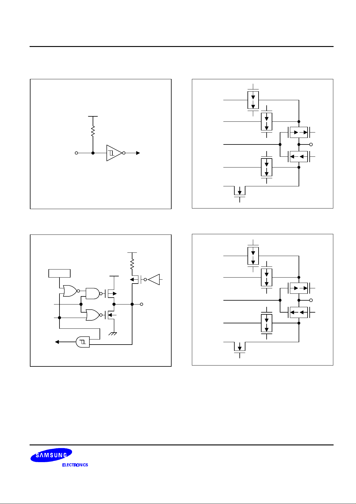
PIN CIRCUIT DIAGRAMS
VLC0
VDD
VLC1
Pull-Up
Resistor
COM
In
Out
Data
Output
Disable
Schmitt Trigger
Figure 1-3. Pin Circuit Type B
VDD
PNE
VDD
P-CH
N-CH
Pull-up
Resistor
Pull-up
Resistor
Enable
I/O
VLC2
VSS
Figure 1-5. Pin Circuit Type H-4
VLC0
VLC1
SEG
VLC2
Out
Schmitt Trigger
Figure 1-4. Pin Circuit Type E-2
VSS
Figure 1-6. Pin Circuit Type H-5
1-7
 Loading...