


查询M470L1624FT0供应商
128MB, 256MB SODIMM
DDR SDRAM SODIMM
200pin Unbuffered SODIMM based on 256Mb F-die
64 / 72-bit (Non ECC / ECC)
DDR SDRAM
Revision 1.2
March, 2004
Rev. 1.2 March 2004

128MB, 256MB SODIMM
Revision History
Revision 1.0 (June, 2003)
- First release
Revision 1.1 (August, 2003)
- Corrected typo.
Revision 1.2 (March, 2004)
- Corrected package dimension.
DDR SDRAM
Rev. 1.2 March 2004
128MB, 256MB SODIMM
DDR SDRAM
200Pin Non ECC / ECC SODIMM based on 256Mb F-die(x16)
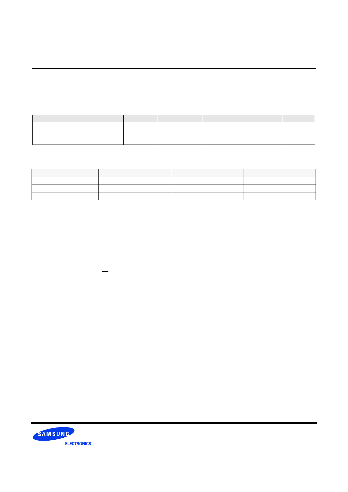
Ordering Information
Part Number Density Organization Component Composition Height
M470L1624FT0-C(L)B3/A2/B0 128MB 16M x 64 16Mx16 (K4H561638F) * 4EA 1,250mil
M470L3224FT0-C(L)B3/A2/B0 256MB 32M x 64 16Mx16 (K4H561638F) * 8EA 1,250mil
M485L1624FT0-C(L)B3/A2/B0 128MB 16M x 72 16Mx16 (K4H561638F) * 5EA
Operating Frequencies
B3(DDR333@CL=2.5) A2(DDR266@CL=2) B0(DDR266@CL=2.5)
Speed @CL2 133MHz 133MHz 100MHz
Speed @CL2.5 166MHz 133MHz 133MHz
CL-tRCD-tRP 2.5-3-3 2-3-3 2.5-3-3
1,250mil
Feature
• Power supply : Vdd: 2.5V ± 0.2V, Vddq: 2.5V ± 0.2V
• Double-data-rate architecture; two data transfers per clock cycle
• Bidirectional data strobe(DQS)
• Differential clock inputs(CK and CK
• DLL aligns DQ and DQS transition with CK transition
• Programmable Read latency 2, 2.5 (clock)
• Programmable Burst length (2, 4, 8)
• Programmable Burst type (sequential & interleave)
• Edge aligned data output, center aligned data input
• Auto & Self refresh, 7.8us refresh interval(8K/64ms refresh)
• Serial presence detect with EEPROM
• PCB : Height 1250 (mil), single(128MB), double(256MB) sided component
)
SAMSUNG ELECTRONICS CO., Ltd. reserves the right to change products and specifications without notice.
Rev. 1.2 March 2004
128MB, 256MB SODIMM
DDR SDRAM
Pin Configurations (Front side/back side)
Pin Front Pin Front Pin Front Pin Back Pin Back Pin Back
1
3
5
7
9
11
13
15
17
19
21
23
25
27
29
31
33
35
37
39
VREF
VSS
DQ0
DQ1
VDD
DQS0
DQ2
VSS
DQ3
DQ8
VDD
DQ9
DQS1
VSS
DQ10
DQ11
VDD
CK0
/CK0
VSS
KEY
41
43
45
47
49
51
53
55
57
59
61
63
65
Note 1. * : These pins are not used in this module.
2. Pins 71, 72, 73, 74, 77, 78, 79, 80, 83, 84 are not used on x64 module, & used on x72 module.
Pin 95,122 are NC for 1Row module (M470L1624FT0, M485L1624FT0) & used for 2Row module (M470L3224FT0).
DQ16
DQ17
VDD
DQS2
DQ18
VSS
DQ19
DQ24
VDD
DQ25
DQS3
VSS
DQ26
67
69
71
73
75
77
79
81
83
85
87
89
91
93
95
97
99
101
103
105
107
109
111
113
115
117
119
121
123
125
127
129
131
133
DQ27
VDD
CB0
CB1
VSS
DQS8
CB2
VDD
CB3
DU
VSS
CK2
/CK2
VDD
CKE1
DU
A12
A9
VSS
A7
A5
A3
A1
VDD
A10/AP
BA0
/WE
/CS0
*DU(A13)
VSS
DQ32
DQ33
VDD
DQS4
135
137
139
141
143
145
147
149
151
153
155
157
159
161
163
165
167
169
171
173
175
177
179
181
183
185
187
189
191
193
195
197
199
DQ34
VSS
DQ35
DQ40
VDD
DQ41
DQS5
VSS
DQ42
DQ43
VDD
VDD
VSS
VSS
DQ48
DQ49
VDD
DQS6
DQ50
VSS
DQ51
DQ56
VDD
DQ57
DQS7
VSS
DQ58
DQ59
VDD
SDA
SCL
VDDSPD
VDDID
2
4
6
8
10
12
14
16
18
20
22
24
26
28
30
32
34
36
38
40
42
44
46
48
50
52
54
56
58
60
62
64
66
VREF
VSS
DQ4
DQ5
VDD
DM0
DQ6
VSS
DQ7
DQ12
VDD
DQ13
DM1
VSS
DQ14
DQ15
VDD
VDD
VSS
VSS
KEY
DQ20
DQ21
VDD
DM2
DQ22
VSS
DQ23
DQ28
VDD
DQ29
DM3
VSS
DQ30
68
70
72
74
76
78
80
82
84
86
88
90
92
94
96
98
100
102
104
106
108
110
112
114
116
118
120
122
124
126
128
130
132
134
DQ31
VDD
CB4
CB5
VSS
DM8
CB6
VDD
CB7
*DU/(RESET)
VSS
VSS
VDD
VDD
CKE0
DU(BA2)
A11
A8
VSS
A6
A4
A2
A0
VDD
BA1
/RAS
/CAS
/CS1
DU
VSS
DQ36
DQ37
VDD
DM4
136
138
140
142
144
146
148
150
152
154
156
158
160
162
164
166
168
170
172
174
176
178
180
182
184
186
188
190
192
194
196
198
200
DQ38
DQ39
DQ44
DQ45
DQ46
DQ47
DQ52
DQ53
DQ54
DQ55
DQ60
DQ61
DQ62
DQ63
VSS
VDD
DM5
VSS
VDD
/CK1
CK1
VSS
VDD
DM6
VSS
VDD
DM7
VSS
VDD
SA0
SA1
SA2
DU
Pin Description
Pin Name Function Pin Name Function
A0 ~ A12 Address input (Multiplexed) DM0 ~ DM7, DM8(for ECC) Data - in mask
BA0 ~ BA1 Bank Select Address VDD Power supply (2.5V)
DQ0 ~ DQ63 Data input/output VDDQ Power Supply for DQS(2.5V)
DQS0 ~ DQS8 Data Strobe input/output VSS Ground
CK0,CK0
CKE0~CKE1 Clock enable input VDDSPD Serial EEPROM Power
CS0
RAS
CAS
WE
CB0 ~ CB7 Check bit(Data-in/data-out)
~ CK2, CK2 Clock input VREF Power supply for reference
~CS1 Chip select input SDA Serial data I/O
Row address strobe SCL Serial clock
Column address strobe SA0 ~ 2 Address in EEPROM
Write enable NC No connection
Rev. 1.2 March 2004
128MB, 256MB SODIMM
DDR SDRAM
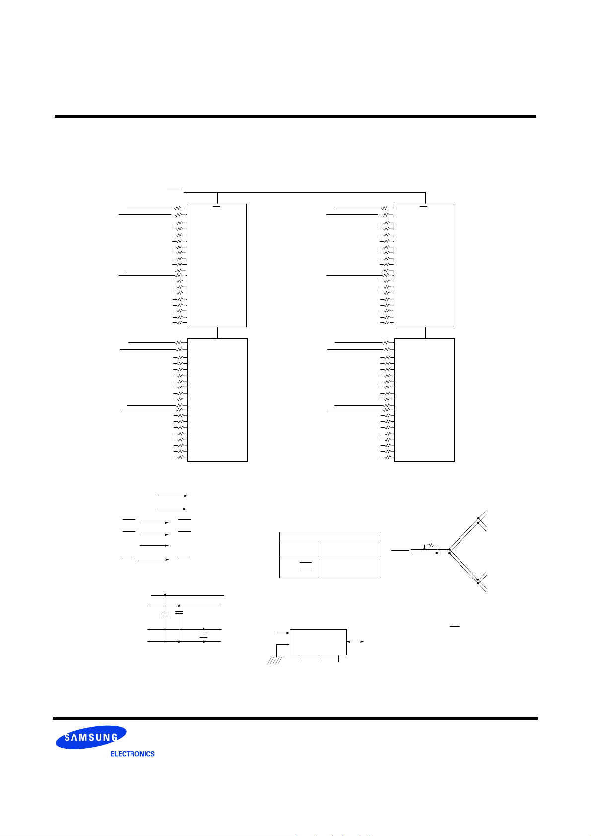
128MB, 16M x 64 Non ECC Module (M470L1624FT0)
FUNCTIONAL BLOCK DIAGRAM
CS0
DQS0
DM0
DQS1
DM1
DQS2
DM2
DQS3
DM3
DQ0
DQ1
DQ2
DQ3
DQ4
DQ5
DQ6
DQ7
DQ8
DQ9
DQ10
DQ11
DQ12
DQ13
DQ14
DQ15
DQ16
DQ17
DQ18
DQ19
DQ20
DQ21
DQ22
DQ23
DQ24
DQ25
DQ26
DQ27
DQ28
DQ29
DQ30
DQ31
LDQS
LDM
I/O 0
I/O 1
I/O 2
I/O 3
I/O 4
I/O 5
I/O 6
I/O 7
UDQS
UDM
I/O 8
I/O 9
I/O 10
I/O 11
I/O 12
I/O 13
I/O 14
I/O 15
LDQS
LDM
I/O 0
I/O 1
I/O 2
I/O 3
I/O 4
I/O 5
I/O 6
I/O 7
UDQS
UDM
I/O 8
I/O 9
I/O 10
I/O 11
I/O 12
I/O 13
I/O 14
I/O 15
CS
D0
CS
D1
DQS4
DM4
DQS5
DM5
DQS6
DM6
DQS7
DM7
(Populated as 1 bank of x16 DDR SDRAM Module)
LDQS
CS
LDM
DQ32
I/O 0
DQ33
I/O 1
I/O 2
I/O 3
I/O 4
I/O 5
I/O 6
I/O 7
UDQS
UDM
I/O 8
I/O 9
I/O 10
I/O 11
I/O 12
I/O 13
I/O 14
I/O 15
LDQS
LDM
I/O 0
I/O 1
I/O 2
I/O 3
I/O 4
I/O 5
I/O 6
I/O 7
UDQS
UDM
I/O 8
I/O 9
I/O 10
I/O 11
I/O 12
I/O 13
I/O 14
I/O 15
D2
CS
D3
DQ34
DQ35
DQ36
DQ37
DQ38
DQ39
DQ40
DQ41
DQ42
DQ43
DQ44
DQ45
DQ46
DQ47
DQ48
DQ49
DQ50
DQ51
DQ52
DQ53
DQ54
DQ55
DQ56
DQ57
DQ58
DQ58
DQ60
DQ61
DQ62
DQ63
BA0 - BA1
A0 - A12
BA0-BA1: DDR SDRAMs D0 - D3
A0-A12: DDR SDRAMs D0 - D3
RAS RAS: SDRAMs D0 - D3
CAS CAS: SDRAMs D0 - D3
CKE0 CKE: SDRAMs D0 - D3
WE
V
DDSPD
V
DD/VDDQ
WE: SDRAMs D0 - D3
SPD
D0 - D3
D0 - D3
VREF
V
SS
D0 - D3
D0 - D3
SCL
WP
Clock
Input
CK0/CK0
CK1/CK1
CK2/CK2
Serial PD
A0
SA0 SA1
Clock Wiring
SDRAMs
2 SDRAMs
2 SDRAMs
A1
A2
SA2
NC
R=120
Ω
Card
Edge
± 5%
CK0/1/2
CK0/1/2
Notes:
1. DQ-to-I/O wiring is shown as recommended but may be changed.
2. DQ/DQS/DM/CKE/CS
be maintained as shown.
SDA
3. DQ, DQS, DM/DQS resistors: 22 Ohms.
relationships must
Rev. 1.2 March 2004
D0/D2/Cap
Cap/Cap/Cap
D1/D3/Cap
Cap/Cap/Cap

128MB, 256MB SODIMM
DDR SDRAM
256MB, 32M x 64 Non ECC Module (M470L3224FT0) (Populated as 2 bank of x16 DDR SDRAM Module)
Functional Block Diagram
CS1
CS0
DQS0
DM0
DQ0
DQ1
DQ2
DQ3
DQ4
DQ5
DQ6
LDQS
LDM
I/0 0
I/0 1
I/0 2
I/0 3
I/0 4
I/0 5
I/0 6
CS
D0
LDQS
LDM
I/0 0
I/0 1
I/0 2
I/0 3
I/0 4
I/0 5
I/0 6
CS
D4
DQS4
DM4
DQ0
DQ1
DQ2
DQ3
DQ4
DQ5
DQ6
LDQS
LDM
I/0 0
I/0 1
I/0 2
I/0 3
I/0 4
I/0 5
I/0 6
CS
D2
LDQS
LDM
I/0 0
I/0 1
I/0 2
I/0 3
I/0 4
I/0 5
I/0 6
CS
D6
DQS1
DM1
DQ0
DQ1
DQ2
DQ3
DQ4
DQ5
DQ6
DQS2
DM2
DQ0
DQ1
DQ2
DQ3
DQ4
DQ5
DQ6
DQS3
DM3
DQ0
DQ1
DQ2
DQ3
DQ4
DQ5
DQ6
BA0 - BA1 BA0-BA1: DDR SDRAMs D0 - D7
A0 - A12
RAS
CAS
CKE0
CKE1
WE
V
DDSPD
V
DD/VDDQ
VREF
V
SS
UDQS
UDM
I/0 8
I/0 9
I/0 10
I/0 11
I/0 12
I/0 13
I/0 14
LDQS
LDM
CS
I/0 0
I/0 1
I/0 2
D1
I/0 3
I/0 4
I/0 5
I/0 6
UDQS
UDM
I/0 8
I/0 9
I/0 10
I/0 11
I/0 12
I/0 13
I/0 14
A0-A12: DDR SDRAMs D0 - D7
RAS: SDRAMs D0 - D7
CAS: SDRAMs D0 - D7
CKE: SDRAMs D0 - D3
CKE: SDRAMs D4 - D7
WE: SDRAMs D0 - D7
SPD
D0 - D7
D0 - D7
D0 - D7
UDQS
UDM
I/0 8
I/0 9
I/0 10
I/0 11
I/0 12
I/0 13
I/0 14
LDQS
LDM
I/0 0
I/0 1
I/0 2
I/0 3
I/0 4
I/0 5
I/0 6
UDQS
UDM
I/0 8
I/0 9
I/0 10
I/0 11
I/0 12
I/0 13
I/0 14
SCL
WP
CS
D5
Clock
Input
CK0/CK0
CK1/CK1
CK2/CK2
A0
SA0 SA1
DQS5
DM5
DQS6
DM6
DQS7
DM7
Clock Wiring
Serial PD
A1
DQ0
DQ1
DQ2
DQ3
DQ4
DQ5
DQ6
DQ0
DQ1
DQ2
DQ3
DQ4
DQ5
DQ6
DQ0
DQ1
DQ2
DQ3
DQ4
DQ5
DQ6
SDRAMs
4 SDRAMs
4 SDRAMs
NC
A2
SA2
SDA
UDQS
UDM
I/0 8
I/0 9
I/0 10
I/0 11
I/0 12
I/0 13
I/0 14
LDQS
CS
LDM
I/0 0
I/0 1
I/0 2
D3
I/0 3
I/0 4
I/0 5
I/0 6
UDQS
UDM
I/0 8
I/0 9
I/0 10
I/0 11
I/0 12
I/0 13
I/0 14
*Clock Net Wiring
Card
Edge
R=120
CK0/1/2
CK0/1/2
Notes:
1. DQ-to-I/O wiring is shown as recommended but may be changed.
2. DQ/DQS/DM/CKE/CS relationships must
be maintained as shown.
3. DQ, DQS, DM/DQS resistors: 22 Ohms.
UDQS
UDM
I/0 8
I/0 9
I/0 10
I/0 11
I/0 12
I/0 13
I/0 14
LDQS
CS
LDM
I/0 0
I/0 1
I/0 2
D7
I/0 3
I/0 4
I/0 5
I/0 6
UDQS
UDM
I/0 8
I/0 9
I/0 10
I/0 11
I/0 12
I/0 13
I/0 14
D0/D2/Cap
D1/D3/Cap
Ω
D4/D6/Cap
D5/D7/Cap
Rev. 1.2 March 2004

128MB, 256MB SODIMM
DDR SDRAM
128MB, 16M x 72 ECC Module (M485L1624FT0) (Populated as 1 bank of x16 DDR SDRAM Module)
Functional Block Diagram
CS0
DQS0
DM0
DQS1
DM1
DQ0
DQ1
DQ2
DQ3
DQ4
DQ5
DQ6
DQ7
DQ8
DQ9
DQ10
DQ11
DQ12
DQ13
DQ14
DQ15
LDQS
LDM
I/O 0
I/O 1
I/O 2
I/O 3
I/O 4
I/O 5
I/O 6
I/O 7
UDQS
UDM
I/O 8
I/O 9
I/O 10
I/O 11
I/O 12
I/O 13
I/O 14
I/O 15
CS
DQS4
DM4
D0
DQS5
DM5
DQ32
DQ33
DQ34
DQ35
DQ36
DQ37
DQ38
DQ39
DQ40
DQ41
DQ42
DQ43
DQ44
DQ45
DQ46
DQ47
LDQS
LDM
I/O 0
I/O 1
I/O 2
I/O 3
I/O 4
I/O 5
I/O 6
I/O 7
UDQS
UDM
I/O 8
I/O 9
I/O 10
I/O 11
I/O 12
I/O 13
I/O 14
I/O 15
CS
D2
DQS8
DM8
CB0
CB1
CB2
CB3
CB4
CB5
CB6
CB7
DQS
DM
I/O 0
I/O 1
I/O 2
I/O 3
I/O 4
I/O 5
I/O 6
I/O 7
UDQS
UDM
I/O 8
I/O 9
I/O 10
I/O 11
I/O 12
I/O 13
I/O 14
I/O 15
CS
D4
DQS2
DM2
DQS3
DM3
BA0 - BA1
A0 - A12
LDQS
CS
LDM
DQ16
I/O 0
DQ17
I/O 1
I/O 2
I/O 3
I/O 4
I/O 5
I/O 6
I/O 7
UDQS
UDM
I/O 8
I/O 9
I/O 10
I/O 11
I/O 12
I/O 13
I/O 14
I/O 15
D1
DQ18
DQ19
DQ20
DQ21
DQ22
DQ23
DQ24
DQ25
DQ26
DQ27
DQ28
DQ29
DQ30
DQ31
BA0-BA1: DDR SDRAMs D0 - D4
A0-A12: DDR SDRAMs D0 - D4
RAS RAS: SDRAMs D0 - D4
CAS CAS: SDRAMs D0 - D4
CKE0 CKE: SDRAMs D0 - D4
WE
V
DDSPD
V
DD/VDDQ
WE: SDRAMs D0 - D4
SPD
D0 - D4
D0 - D4
VREF
V
SS
D0 - D4
D0 - D4
DQS6
DM6
DQS7
DM7
SCL
WP
Clock
Input
CK0/CK0
CK1/CK1
CK2/CK2
Serial PD
A0
SA0 SA1
DQ48
DQ49
DQ50
DQ51
DQ52
DQ53
DQ54
DQ55
DQ56
DQ57
DQ58
DQ58
DQ60
DQ61
DQ62
DQ63
Clock Wiring
A1
LDQS
LDM
I/O 0
I/O 1
I/O 2
I/O 3
I/O 4
I/O 5
I/O 6
I/O 7
UDQS
UDM
I/O 8
I/O 9
I/O 10
I/O 11
I/O 12
I/O 13
I/O 14
I/O 15
SDRAMs
2 SDRAMs
2 SDRAMs
1 SDRAMs
A2
SA2
CS
D3
R=120
Ω
Card
Edge
± 5%
CK0/1/2
CK0/1/2
Notes:
1. DQ-to-I/O wiring is shown as recommended but may be changed.
SDA
2. DQ/DQS/DM/CKE/CS relationships must
be maintained as shown.
3. DQ, DQS, DM/DQS resistors: 22 Ohms.
D0/D2/D4
Cap/Cap/Cap
D1/D3/Cap
Cap/Cap/Cap
Rev. 1.2 March 2004

128MB, 256MB SODIMM
DDR SDRAM
Absolute Maximum Ratings
Parameter Symbol Value Unit
Voltage on any pin relative to Vss V
Voltage on V
Voltage on V
DD supply relative to Vss VDD -1.0 ~ 3.6 V
DDQ supply relative to Vss VDDQ -1.0 ~ 3.6 V
Storage temperature T
Power dissipation P
Short circuit current I
Note :
Permanent device damage may occur if ABSOLUTE MAXIMUM RATINGS are exceeded.
IN, VOUT -0.5 ~ 3.6 V
STG -55 ~ +150 °C
D 1.5 * # of component W
OS 50 mA
Functional operation should be restricted to recommended operating condition.
Exposure to higher than recommended voltage for extended periods of time could affect device reliability.
Power & DC Operating Conditions (SSTL_2 In/Out)
Recommended operating conditions(Voltage referenced to V
Parameter Symbol Min Max Unit Note
Supply voltage(for device with a nominal VDD of 2.5V) VDD 2.3 2.7 5
I/O Supply voltage V
I/O Reference voltage V
I/O Termination voltage(system) V
Input logic high voltage V
Input logic low voltage V
Input Voltage Level, CK and CK
Input Differential Voltage, CK and CK
V-I Matching: Pullup to Pulldown Current Ratio VI(Ratio) 0.71 1.4 - 4
Input leakage current I
Output leakage current I
Output High Current(Normal strengh driver) ;V
V
+ 0.84V
TT
Output High Current(Normal strengh driver) ;V
V
- 0.84V
TT
Output High Current(Half strengh driver) ;V
+ 0.45V
inputs VIN(DC) -0.3 VDDQ+0.3 V
inputs VID(DC) 0.36 VDDQ+0.6 V 3
OUT
OUT
= VTT
OUT
SS=0V, TA=0 to 70°C)
DDQ 2.3 2.7 V 5
IH(DC) VREF+0.15 VDDQ+0.3 V
IL(DC) -0.3 VREF-0.15 V
=
=
I
I
I
REF 0.49*VDDQ 0.51*VDDQ V 1
TT
I -2 2 uA
OZ -5 5 uA
OH -16.8 mA
OL 16.8 mA
OH -9 mA
VREF-0.04 VREF+0.04 V 2
Notes 1. Includes ± 25mV margin for DC offset on VREF, and a combined total of ± 50mV margin for all AC noise and DC offset on VREF,
2.V
bandwidth limited to 20MHz. The DRAM must accommodate DRAM current spikes on V
TO V
REF, both of which may result in VREF noise. VREF should be de-coupled with an inductance of ≤ 3nH.
is not applied directly to the device. VTT is a system supply for signal termination resistors, is expected to be set equal to
TT
V
REF, and must track variations in the DC level of VREF
REF and internal DRAM noise coupled
3. VID is the magnitude of the difference between the input level on CK and the input level on CK.
4. These parameters should be tested at the pin on actual components and may be checked at either the pin or the pad in
simulation. The AC and DC input specifications are relative to a VREF envelop that has been bandwidth limited to 200MHZ.
Rev. 1.2 March 2004

128MB, 256MB SODIMM
DDR SDRAM
M470L1624FT0 (16M x 64, 128MB Module)
(VDD=2 .7V, T = 10°C)
Symbol B3(DDR333@CL=2.5) A2(DDR266@CL=2) B0(DDR266@CL=2.5) Unit Notes
IDD0 360 320 320 mA
IDD1 500 460 460 mA
IDD2P 12 12 12 mA
IDD2F 100 80 80 mA
IDD2Q 80 72 72 mA
IDD3P 140 120 120 mA
IDD3N 220 180 180 mA
IDD4R 800 680 680 mA
IDD4W 760 620 620 mA
IDD5 720 660 660 mA
IDD6 Normal 12 12 12 mA
Low power 6 6 6 mA Optional
IDD7A 1,400 1,200 1,200 mA
* Module IDD was calculated on the basis of component IDD and can be differently measured according to DQ loading cap.
M470L3224FT0 (32M x 64, 256MB Module)
(VDD=2.7V, T = 10°C)
Symbol B3(DDR333@CL=2.5) A2(DDR266@CL=2) B0(DDR266@CL=2.5) Unit Notes
IDD0 580 500 500 mA
IDD1 720 640 640 mA
IDD2P 24 24 24 mA
IDD2F 200 160 160 mA
IDD2Q 160 144 144 mA
IDD3P 280 240 240 mA
IDD3N 440 360 360 mA
IDD4R 1,020 860 860 mA
IDD4W 980 800 800 mA
IDD5 940 840 840 mA
IDD6 Normal 24 24 24 mA
Low power 12 12 12 mA Optional
IDD7A 1,620 1,380 1,380 mA
* Module IDD was calculated on the basis of component IDD and can be differently measured according to DQ loading cap.
Rev. 1.2 March 2004

128MB, 256MB SODIMM
DDR SDRAM
M485L1624FT0 (16M x 72, 128MB Module)
(VDD=2.7V, T = 10°C)
Symbol B3(DDR333@CL=2.5) A2(DDR266@CL=2) B0(DDR266@CL=2.5) Unit Notes
IDD0 810 720 720 mA
IDD1 1,035 900 900 mA
IDD2P 27 27 27 mA
IDD2F 225 180 180 mA
IDD2Q 180 162 162 mA
IDD3P 315 270 270 mA
IDD3N 495 405 405 mA
IDD4R 1,260 1,080 1,080 mA
IDD4W 1,440 1,215 1,215 mA
IDD5 1,530 1,440 1,440 mA
IDD6 Normal 27 27 27 mA
Low power 14 14 14 mA Optional
IDD7A 2,340 2,160 2,160 mA
* Module IDD was calculated on the basis of component IDD and can be differently measured according to DQ loading cap.
Rev. 1.2 March 2004

128MB, 256MB SODIMM
DDR SDRAM
AC Operating Conditions
Parameter/Condition Symbol Min
Input High (Logic 1) Voltage, DQ, DQS and DM signals VIH(AC) VREF + 0.31 V 3
Input Low (Logic 0) Voltage, DQ, DQS and DM signals. VIL(AC) VREF - 0.31 V 3
Input Differential Voltage, CK and CK inputs VID(AC) 0.7 VDDQ+0.6 V 1
Input Crossing Point Voltage, CK and CK inputs VIX(AC) 0.5*VDDQ-0.2 0.5*VDDQ+0.2 V 2
Note 1. VID is the magnitude of the difference between the input level on CK and the input on CK.
2. The value of V
3. These parameters should be tested at the pim on actual components and may be checked at either the pin or the pad in simulation. the AC and DC input specificatims are refation to a Vref envelope that has been bandwidth limited 20MHz.
is expected to equal 0.5*V
IX
of the transmitting device and must track variations in the DC level of the same.
DDQ
Vtt=0.5*VDDQ
RT=50Ω
Max
Unit Note
Output
Z0=50Ω
LOAD=30pF
C
V
REF
=0.5*VDDQ
Output Load Circuit (SSTL_2)
Input/Output Capacitance (VDD=2.5V, VDDQ=2.5V, TA= 25°C, f=1MHz)
Parameter Symbol
Input capacitance(A0 ~ A12, BA0 ~ BA1,RAS,CAS,WE )CIN1414549574145pF
Input capacitance(CKE0, CKE1) CIN2 34 38 42 50 34 38 pF
Input capacitance( CS0
Input capacitance( CLK0, CLK1,CLK2) CIN4 25 30 25 30 25 30 pF
Input capacitance(DM0~DM7,DM8(for ECC)) CIN5 6 7 6 7 6 7 pF
Data & DQS input/output capacitance(DQ0~DQ63) Cout1 6 7 6 7 6 7 pF
Data input/output capacitance (CB0~CB7) Cout2 - - - - 6 7 pF
, CS1) CIN3343842503438pF
M470L1624FT0 M470L3224FT0 M485L1624FT0
Min Max Min Max Min Max
Unit
Rev. 1.2 March 2004

128MB, 256MB SODIMM
AC Timming Parameters & Specifications
DDR SDRAM
Parameter Symbol
B3
(DDR333@CL=2.5))
A2
(DDR266@CL=2.0)
B0
(DDR266@CL=2.5))
Unit Note
Min Max Min Max Min Max
Row cycle time tRC 60 65 65 ns
Refresh row cycle time tRFC 72 75 75 ns
Row active time tRAS 42 70K 45 120K 45 120K ns
RAS to CAS delay tRCD182020ns
Row precharge time tRP 18 20 20 ns
Row active to Row active delay tRRD 12 15 15 ns
Write recovery time tWR 15 15 15 ns
Last data in to Read command tWTR 1 1 1 tCK
Col. address to Col. address delay tCCD 1 1 1 tCK
Clock cycle time
Clock high level width tCH 0 .45 0.55 0.45 0.55 0.45 0.55 tCK
Clock low level width tCL 0.45 0.55 0.45 0.55 0.45 0.55 tCK
DQS-out access time from CK/CK tDQSCK -0.6 +0.6 -0.75 +0.75 -0.75 +0.75 ns
Output data access time from CK/CK tAC -0.7 +0.7 -0.75 +0.75 -0.75 +0.75 ns
Data strobe edge to ouput data edge tDQSQ - 0.45 - 0.5 - 0.5 ns 12
Read Preamble tRPRE 0.9 1.1 0.9 1.1 0.9 1.1 tCK
Read Postamble tRPST 0.4 0.6 0.4 0.6 0.4 0.6 tCK
CK to valid DQS-in tDQSS 0.75 1.25 0.75 1.25 0.75 1.25 t CK
DQS-in setup time tWPRES 0 0 0 ns 3
DQS-in hold time tWPRE 0.25 0.25 0.25 tCK
DQS falling edge to CK rising-setup time tDSS 0.2 0.2 0.2 tCK
DQS falling edge from CK rising-hold time tDSH 0.2 0.2 0.2 tCK
DQS-in high level width tDQSH 0.35 0.35 0.35 tCK
DQS-in low level width tDQSL 0.35 0.35 0.35 tCK
DQS-in cycle time tDSC 0.9 1.1 0.9 1.1 0.9 1.1 tCK
Address and Control Input setup time(fast) tIS 0.75 0.9 0.9 ns i,5.7~9
Address and Control Input hold time(fast) tIH 0.75 0.9 0.9 ns i,5.7~9
Address and Control Input setup time(slow) tIS 0.8 1.0 1.0 ns i, 6~9
Address and Control Input hold time(slow) tIH 0.8 1.0 1.0 ns i, 6~9
Data-out high impedence time from CK/CK tHZ +0.7 +0.75 +0.75 ns 1
Data-out low impedence time from CK/CK tLZ -0.7 +0.7 -0.75 +0.75 -0.75 +0.75 ns 1
CL=2.0
CL=2.5 6 12 7.5 12 7.5 12 ns
tCK
7.5 12 7.5 12 10 12 ns
Rev. 1.2 March 2004

128MB, 256MB SODIMM
DDR SDRAM
B3
Parameter Symbol
(DDR333@CL=2.5))
Min Max Min Max Min Max
Mode register set cycle time tMRD 12 15 15 ns
DQ & DM setup time to DQS tDS 0.45 0.5 0.5 ns j, k
DQ & DM hold time to DQS tDH
Control & Address input pu lse width tIPW 2.2 2.2 2.2 ns 8
DQ & DM input pulse width tDIPW 1.75 1.75 1.75 ns 8
Power down exit time tPDEX 6 7.5 7.5 ns
Exit self refresh to non-Read command tXSNR 75 75 75 ns
Exit self refresh to read command tXSRD 200 200 200 tCK
Refresh interval time tREFI 7.8 7.8 7.8 us 4
Output DQS valid window tQH
Clock half period tHP
Data hold skew factor tQH S 0.55 0.75 0.75 ns 11
DQS write postamble time tWPST 0.4 0.6 0.4 0.6 0.4 0.6 tCK 2
Active to Read with Auto precharge
command
Autoprecharge write recovery +
Precharge time tDAL
tRAP 18 20 20
0.45 0.5 0.5
tHP
-tQHS
tCLmin
or tCHmin
(tWR/tCK)
+
(tRP/tCK)
-
or tCHmin
(tWR/tCK)
(tRP/tCK)
A2
(DDR266@CL=2.0)
tHP
-tQHS
tCLmin
+
B0
(DDR266@CL=2.5))
-
-
tHP
-tQHS
tCLmin
or tCHmin
(tWR/tCK)
+
(tRP/tCK)
Unit Note
ns
-ns11
- ns 10, 11
tCK 13
j, k
System Characteristics for DDR SDRAM
The following specification parameters are required in systems using DDR333 & DDR266 devices to ensure proper system performance. these characteristics are for system simulation purposes and are guaranteed by design.
Table 1 : Input Slew Rate for DQ, DQS, and DM
AC CHARACTERISTICS DDR333 DDR266
PARAMETER SYMBOL MIN MAX MIN MAX Units Notes
DQ/DM/DQS input slew rate measured between
VIH(DC), VIL(DC) and VIL(DC), VIH(DC)
Table 2 : Input Setup & Hold Time Derating for Slew Rate
Input Slew Rate tIS tIH Units Notes
0.5 V/ns 0 0 ps i
0.4 V/ns +50 0 ps i
0.3 V/ns +10 0 0 ps i
Table 3 : Input/Output Setup & Hold Time Derating for Slew Rate
Input Slew Rate tDS tDH Units Notes
0.5 V/ns 0 0 ps k
0.4 V/ns +75 +75 ps k
0.3 V/ns +150 +150 ps k
DCSLEW TBD TBD TBD TBD V/ns a, m
Rev. 1.2 March 2004

128MB, 256MB SODIMM
Table 4 : Input/Output Setup & Hold Derating for Rise/Fall Delta Slew Rate
Delta Slew Rate tDS tDH Units Notes
+/- 0.0 V/ns 0 0 ps j
+/- 0.25 V/ns +50 +50 ps j
+/- 0.5 V/ns +100 +100 ps j
Table 5 : Output Slew Rate Characteristice (X4, X8 Devices only)
Slew Rate Characteristic
Pullup Slew Rate 1.2 ~ 2.5 1.0 4.5 a,c,d,f,g,h
Pulldown slew 1.2 ~ 2.5 1.0 4.5 b,c,d,f,g,h
Typical Range
(V/ns)
Table 6 : Output Slew Rate Characteristice (X16 Devices only)
Slew Rate Characteristic
Pullup Slew Rate 1.2 ~ 2.5 0.7 5.0 a,c,d,f,g,h
Pulldown slew 1.2 ~ 2.5 0.7 5.0 b,c,d,f,g,h
Typical Range
(V/ns)
Table 7 : Output Slew Rate Matching Ratio Characteristics
AC CHARACTERISTICS DDR333 DDR266
PARAMETER MIN MAX MIN MAX Notes
Output Slew Rate Matching Ratio (Pullup to Pulldown) TBD TBD TBD TBD e,m
Minimum
(V/ns)
Minimum
(V/ns)
Maximum
(V/ns)
Maximum
(V/ns)
Notes
Notes
DDR SDRAM
Rev. 1.2 March 2004

128MB, 256MB SODIMM
DDR SDRAM
Component Notes
1. tHZ and tLZ transitions occur in the same access time windows as valid data transitions. these parameters are not referenced to a
specific voltage level but specify when the device output in no longer driving (HZ), or begins driving (LZ).
2. The maximum limit for this parameter is not a device limit. The device will operate with a greater value for this parameter, but sys
tem performance (bus turnaround) will degrade accordingly.
3. The specific requirement is that DQS be valid (HIGH, LOW, or at some point on a valid transition) on or before this CK edge. A
valid transition is defined as monotonic and meeting the input slew rate specifications of the device. when no writes were previ
ously in progress on the bus, DQS will be tran sitioning from High- Z to logic LOW. If a previous write was in progress, DQS could
be HIGH, LOW, or transitioning from HIGH to LOW at this time, depending on tDQSS.
4. A maximum of eight AUTO REFRESH commands can be posted to any given DDR SDRAM device.
5. For command/address input slew rate ≥ 1.0 V/ns
6. For command/address input slew rate ≥ 0.5 V/ns and < 1.0 V/ns
7. For CK & CK
8. These parameters guarantee device timing, but they are not necessarily tested on each device. They may be guaranteed by
device design or tester correlation.
9. Slew Rate is measured between VOH(ac) and VOL(ac).
10. Min (tCL, tCH) refers to the smaller of the actual clock low time and the actual clock high time as provided to the device (i.e. this
value can be greater than the minimum specification limits for tCL and tCH).....For example, tCL and tCH are = 50% of the
period, less the half period jitter (tJIT(HP)) of the clock source, and less the half period jitter due to crosstalk (tJIT(crosstalk)) into
the clock traces.
11. tQH = tHP - tQHS, where:
tHP = minimum half clock period for any given cycle and is defined by clock high or clock low (tCH, tCL). tQHS accounts for 1) The
pulse duration distortion of on-chip clock circuits; and 2) The worst case push-out of DQS on one tansition followed by the worst
case pull-in of DQ on the next transition, both of which are, separately, due to data pin skew and output pattern effects, and p channel to n-channel variation of the output drivers.
12. tDQSQ
Consists of data pin skew and output pattern effects, and p-channel to n-channel variation of the output drivers for any given
cycle.
13. tDAL = (tWR/tCK) + (tRP/tCK)
For each of the terms above, if not already an integer, round to the next highest integer. Example: For DDR266B at CL=2.5 and
tCK=7.5ns tDAL = (15 ns / 7.5 ns) + (20 ns/ 7.5ns) = (2) + (3)
tDAL = 5 clocks
slew rate ≥ 1.0 V/ns
Rev. 1.2 March 2004

128MB, 256MB SODIMM
System Notes :
a. Pullup slew rate is characteristized under the test conditions as shown in Figure 1.
DDR SDRAM
Test point
Output
Ω
50
VSSQ
Figure 1 : Pullup slew rate test load
b. Pulldown slew rate is measured under the test conditions shown in Figure 2.
VDDQ
50Ω
Output
Test point
Figure 2 : Pulldown slew rate test load
c. Pullup slew rate is measured between (VDDQ/2 - 320 mV +/- 250 mV)
Pulldown slew rate is measured between (VDDQ/2 + 320 mV +/- 250 mV)
Pullup and Pulldown slew rate conditions are to be met for any pattern of data, including all outputs switching and only one output
switching.
Example : For typical slew rate, DQ0 is switching
For minmum slew rate, all DQ bits are switching from either high to low, or low to high.
The remaining DQ bits remain the same as for previous state.
d. Evaluation conditions
Typical : 25 °C (T Ambient), VDDQ = 2.5V, typical process
Minimum : 70 °C (T Ambient), VDDQ = 2.3V, slow - slow process
Maximum : 0 °C (T Ambient), VDDQ = 2.7V, fast - fast process
e. The ratio of pullup slew rate to pulldown slew rate is specified for the same temperature and voltage, over the entire temperature and
voltage range. For a given output, it represents the maximum dif f erence between pullup and pulldown drivers due to process variation.
f. Verified under typical conditions for qualification purposes.
g. TSOPII package divices only.
h. Only intended for operation up to 266 Mbps per pin.
i. A derating factor will be used to increase tIS and tIH in the case where the input slew rate is below 0.5V/ns
as shown in Table 2. The Input slew rate is based on the lesser of the slew rates detemined by either VIH(AC) to VIL(AC) or
VIH(DC) to VIL(DC), similarly for rising transitions.
j. A derating factor will be used to increase tDS and tDH in the case where DQ, DM, and DQS slew rates dif fer, as shown in Tables 3 & 4.
Input slew rate is based on the larger of AC-AC delta rise, fall rate and DC-DC delta rise, Input slew rate is based on the lesser of the
slew rates determined by either VIH(AC) to VIL(AC) or VIH(DC) to VIL(DC), similarly for rising transitions.
The delta rise/fall rate is calculated as: {1/(Slew Rate1)} - {1/(Slew Rate2)}
For example : If Slew Rate 1 is 0.5 V/ns and slew Rate 2 is 0.4 V/ns, then the delta rise, fall rate is - 0.5ns/V . Using the t able given, this
would result in the need for an increase in tDS and tDH of 100 ps.
k. Table 3 is used to increase tDS and tDH in the case where the I/O slew rate is below 0.5 V/ns. The I/O slew rate is based on the lesser
on the lesser of the AC - AC slew rate and the DC- DC slew rate. The inut slew rate is based on the lesser of the slew rates deter
mined by either VIH(ac) to VIL(ac) or VIH(DC) to VIL(DC), and similarly for rising transitions.
m. DQS, DM, and DQ input slew rate is specified to prevent double clocking of data and preserve setup and hold times. Signal transi
tions through the DC region must be monotoy.
Rev. 1.2 March 2004

128MB, 256MB SODIMM
(V=Valid, X=Don′t Care, H=Logic High, L=Logic Low)
Command Truth Table
COMMAND
CKEn-1 CKEn CS RAS CAS WE BA0,1 A10/AP
DDR SDRAM
A0 ~ A9,
A11, A12
Register Extended MRS H X L L L L OP CODE 1, 2
Register Mode Register Set H X L L L L OP CODE 1, 2
Refresh
Auto Refresh
Self
Refresh
Entry L 3
H
Exit L H
H
LL LH X
LHHH
HX XX 3
X
Bank Active & Row Addr. H X L L H H V Row Address
Read &
Column Address
Write &
Column Address
Auto Precharge Disable
Auto Precharge Enable H 4
Auto Precharge Disable
Auto Precharge Enable H 4, 6
HXLHLHV
HXLHLLV
L
L
Column
Address
Column
Address
Burst Stop H X L H H L X 7
Precharge
Active Power Down
Bank Selection
All Banks X H 5
Entry H L
HXLLHL
HX XX
VL
XLVVV
X
Exit L H X X X X
Entry H L
Precharge Power Down Mode
Exit L H
HX XX
LHHH
HX XX
LVVV
X
DM H X X 8
No operation (NOP) : Not defined H X
HX XX
LHHH 9
X
Note
3
3
4
4
9
Note : 1. OP Code : Operand Code. A0 ~ A12 & BA0 ~ BA1 : Program keys. (@EMRS/MRS)
2. EMRS/ MRS can be issued only at all banks precharge state.
A new command can be issued 2 clock cycles after EMRS or MRS.
3. Auto refresh functions are same as the CBR refresh of DRAM.
The automatical precharge without row precharge command is meant by "Auto".
Auto/self refresh can be issued only at all banks precharge state.
4. BA
If both BA
If BA
If BA
If both BA
5. If A
0 ~ BA1 : Bank select addresses.
0 and BA1 are "Low" at read, write, row active and precharge, bank A is selected.
0 is "High" and BA1 is "Low" at read, write, row active and precharge, bank B is selected.
0 is "Low" and BA1 is "High" at read, write, row active and precharge, bank C is selected.
0 and BA1 are "High" at read, write, row active and precharge, bank D is selected.
10/AP is "High" at row precharge, BA0 and BA1 are ignored and all banks are selected.
6. During burst write with auto precharge, new read/write command can not be issued.
Another bank read/write command can be issued after the end of burst.
New row active of the associated bank can be issued at t
RP after the end of burst.
7. Burst stop command is valid at every burst length.
8. DM sampled at the rising and falling edges of the DQS and Data-in are masked at the both edges (Write DM latency is 0).
9. This combination is not defined for any function, which means "No Operation(NOP)" in DDR SDRAM.
Rev. 1.2 March 2004

128MB, 256MB SODIMM
Physical Dimensions : 16M x64 (M470L1624FT0)
2.70
(67.60)
2.50
(63.60)
0.16 ± 0.039
(4.00
± 0.10)
0.24
(6.0)
1
39 41
199
DDR SDRAM
Units : Inches (Millimeters)
Full R 2x
1.25
0.79
(31.75)
(20.00)
0.157 Min
(4.00 Min)
0.086
2.15
0.098
2.45
0.150 Max
(3.80 Max)
0.157 Min
(4.00 Min)
0.04 ± 0.0039
(1.00 ± 0.10)
0.456
11.40
0.07
(1.8)
2
0.17
(4.20)
0.096
(2.40)
Z Y
40 42
Detail Z
1.896
(47.40)
0.04
± 0.0039
(1.00 ± 0.1)
0.16 ± 0.0039
(4.00
± 0.10)
200
0.102 Min
2-φ 0.07
(1.80)
(2.55 Min)
0.018
0.024 TYP
(0.60 TYP)
Detail Y
± 0.001
(0.45 ± 0.03)
0.01
(0.25)
Tolerances : ±.006(.15) unless otherwise specified
The used device is 16Mx16 DDR SDRAM, TSOPII
DDR SDRAM Part No. : K4H561638F-T***
Rev. 1.2 March 2004

128MB, 256MB SODIMM
Physical Dimensions : 32M x64 (M470L3224FT0)
2.70
(67.60)
2.50
(63.60)
0.16 ± 0.039
(4.00
± 0.10)
0.24
(6.0)
1
39 41
199
DDR SDRAM
Units : Inches (Millimeters)
Full R 2x
1.25
0.79
(31.75)
(20.00)
0.157 Min
(4.00 Min)
0.086
2.15
0.098
2.45
0.150 Max
(3.80 Max)
0.157 Min
(4.00 Min)
0.04 ± 0.0039
(1.00 ± 0.10)
0.456
11.40
0.07
(1.8)
2
0.17
(4.20)
0.096
(2.40)
Z Y
40 42
Detail Z
1.896
(47.40)
0.04
± 0.0039
(1.00 ± 0.1)
0.16 ± 0.0039
(4.00
± 0.10)
200
0.102 Min
2-φ 0.07
(1.80)
(2.55 Min)
0.018
0.024 TYP
(0.60 TYP)
Detail Y
± 0.001
(0.45 ± 0.03)
0.01
(0.25)
Tolerances : ±.006(.15) unless otherwise specified
The used device is 16Mx16 DDR SDRAM, TSOPII
DDR SDRAM Part No. : K4H561638F-T***
Rev. 1.2 March 2004

128MB, 256MB SODIMM
Physical Dimensions : 16M x72 (M485L1624FT0)
2.70
(67.60)
2.50
(63.60)
0.16 ± 0.039
(4.00
± 0.10)
0.24
(6.0)
1
39 41
199
DDR SDRAM
Units : Inches (Millimeters)
Full R 2x
1.25
0.79
(31.75)
(20.00)
0.157 Min
(4.00 Min)
0.086
2.15
0.098
2.45
0.150 Max
(3.80 Max)
0.157 Min
(4.00 Min)
0.04 ± 0.0039
(1.00 ± 0.10)
0.456
11.40
0.07
(1.8)
2
0.17
(4.20)
0.096
(2.40)
Z Y
40 42
Detail Z
1.896
(47.40)
0.04
± 0.0039
(1.00 ± 0.1)
0.16 ± 0.0039
(4.00 ± 0.10)
200
0.102 Min
2-φ 0.07
(1.80)
(2.55 Min)
0.018
0.024 TYP
(0.60 TYP)
Detail Y
± 0.001
(0.45 ± 0.03)
0.01
(0.25)
Tolerances : ±.006(.15) unless otherwise specified
The used device is 16Mx16 DDR SDRAM, TSOPII
DDR SDRAM Part No. : K4H561638F-T***
Rev. 1.2 March 2004
 Loading...