

Samsung KS9287 Datasheet

DIGITAL SIGNAL PROCESSOR KS9287
KS9287
PRELIMINARY
DATA SHEET
1999.6.7
1
DIGITAL SIGNAL PROCESSOR KS9287
INTRODUCTION
The KS9287 is a Digital Signal Processor for VCD and Hi-Fi CD players. It has enhanced the picture quality of
VCD. This IC, when compared to the existing product, has vastly improved its performance in the following areas.
— Frame Sync Detect
— Error Correcting Code Ability
— CLV Performance
— DPLL Capture Range
— EFM Signal Compensation
FEATURES
• EFM data demodulation
• Enhanced Frame sync detection/protection/insertion
• Error Correction (C1: double correction, C2: double correction / quadruple correction)
• Interpolation
• Subcode Data serial output
• Enhanced CLV servo controller
• Enhanced DPLL
• MICOM Interface
• Digital Audio Out
• Built-in 16 K SRAM
• 2x Playback Capability
• 5 V +/- 10% Single Power Supply
• CMOS Process
ORDERING INFORMATION
Device Package Operating Temperature
KS9287 80-QFP-1420C -20 °C ~ +75 °C
2

DIGITAL SIGNAL PROCESSOR KS9287
BLOCK DIAGRAM
S0S1 SBCK SBDT
EFMI
APDO
VCOI
CNTVOL
DPFIN
DPFOUT
DPDO
SMEF
SMON
SMDP
SMDS
LOCK
EFM
Phase
Detector
DPLL
CLV
Servo
Subcode
Sync
Detector
Shift
Register
Fsync
Detector
Protector
Insertor
Subcode
Out
EFM
Demodulator
Subcode-Q
Register
ECC
16K
SRAM
SQDT
SQCK
XIN
XOUT
MCK
MDAT
MLT
TEST
X'tal
Timing
Generator
Micom
Interface
Mode
Selector
XTALSEL,DPLL,
CDROM, SRAM,
DSPEED
Tracking
Counter
Digital
Out
TRCNT /ISTAT DATX
Address
Generator
Inter-
polator
C2PO, SADT,
BCK, LRCH,
WDCH
8bit
data
bus
3
DIGITAL SIGNAL PROCESSOR KS9287
RESET
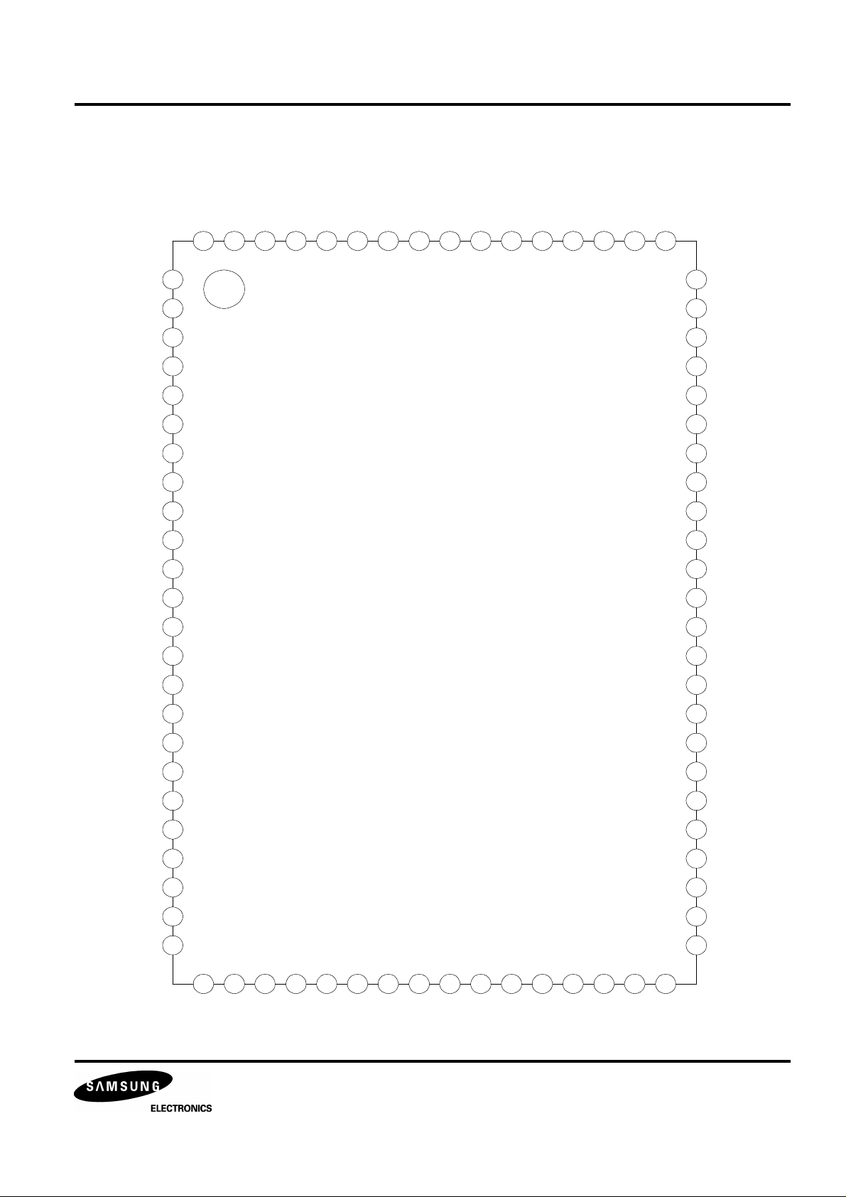
PIN CONFIGURATION
VDDA
DPDO
DPFIN
DPFOUT
CNTVOL
VSSA
DATX
XIN
XOUT
WDCH
LRCH
SADT
VSS
BCK
APDO
80 79 78 77 76 75 74 73 72 71 70 69 68 67 66 65
1
2
3
4
5
6
7
8
9
10
11
12
13
VCOI
DSPEED
VCOO
SMDS
SMDP
VDD
SMON
SMEF
WBCK
LOCK
TRCNT
/ISTAT
KS9287
14
DSVO
EFMI
TEST1
64
63
62
61
60
59
58
57
56
55
54
53
52
51
SRAM
CDROM
DPLL
XTALSEL
/CS
/WE
C16M
C4M
/JIT
ULKFS
FSDW
VSS
/PBCK
FLAG5
C2PO
TIM2
EFMFLAG
UDTFLAG
FSYNC
EFMZ
V34M
TEST0
RBCK
EMPH
15
16
17
18
19
20
21
22
23
24
25 26 27 28 29 30 31 32 33 34 35 36 37 38 39 40
LKFS
S0S1
SQEN
SQCK
SQDT
SQOK
SBCK
SBDT
VDD
MUTE
MLT
MDAT
MCK
RD7
RD6
50
49
48
47
46
45
44
43
42
41
FLAG4
FLAG3
FLAG2
FLAG1
RD0
RD1
RD2
RD3
RD4
RD5
4
DIGITAL SIGNAL PROCESSOR KS9287
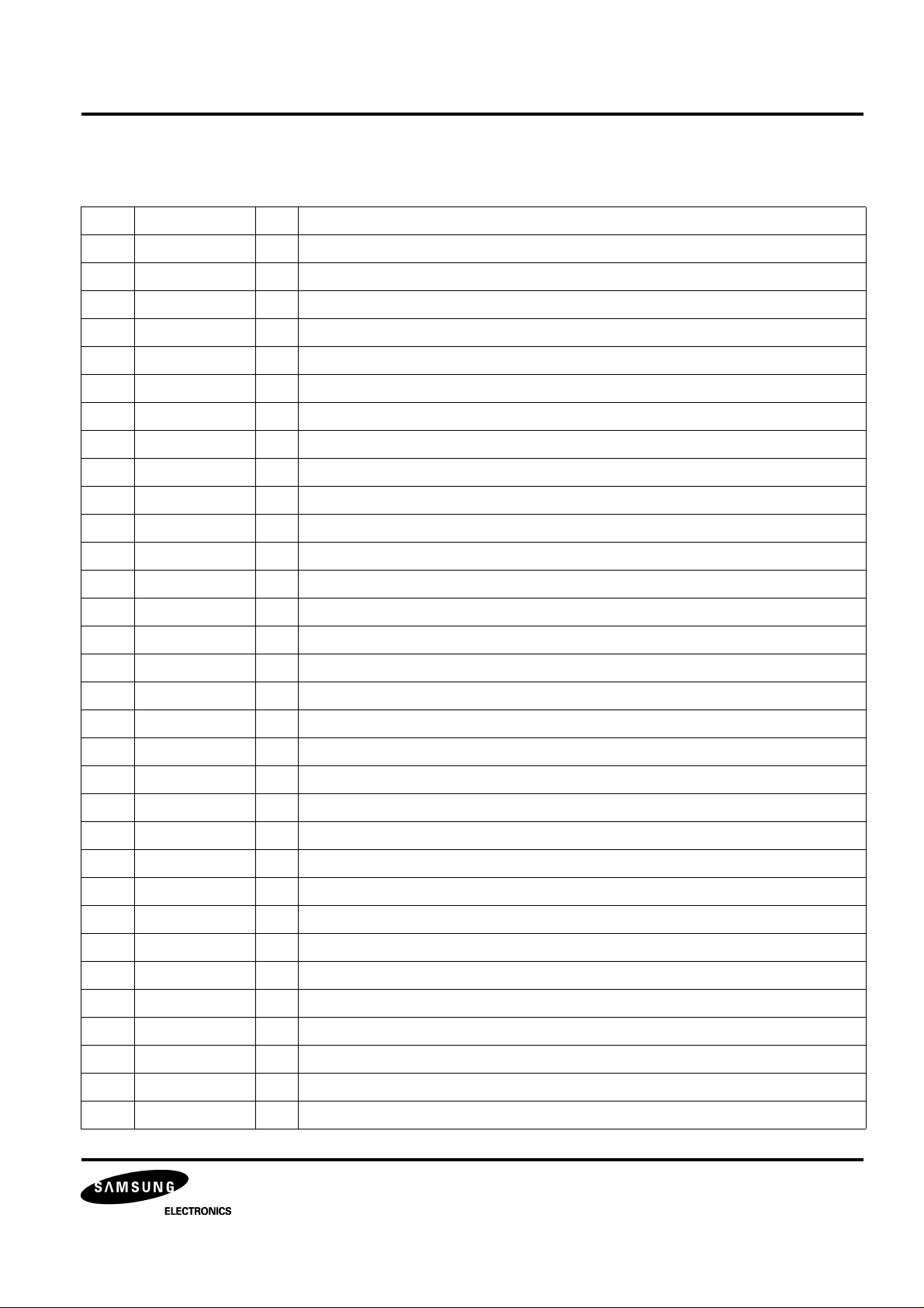
PIN DESCRIPTION
No. Pin Name I/O Description
1 VDDA - Analog VDD
2 DPDO O Charge pump output for Digital PLL
3 DPFIN I Filter input for Digital PLL
4 DPFOUT O Filter output for Digital PLL
5 CNTVOL I VCO control voltage for Digital PLL
6 VSSA - Analog Ground
7 DATX O Digital Audio Serial Output
8 XIN I X'tal oscillator input
9 XOUT O X'tal oscillator output
10 WDCH O Word clock output of 48 bits/Slot (88.2 kHz)
11 LRCH O Channel clock output of 48 bits/Slot (44.1 kHz)
12 SADT O Serial audio data output of 48 bits/Slot (MSB first)
13 VSS - Digital Ground
14 BCK O Bit clock output of 48 bits/Slot (2.1168 MHz)
15 C2PO O C2 Pointer for Serial audio data
16 TIM2 O Normal or Double speed control output
17 EFMFLAG O 8 to14 demodulation error flag
18 UDTFLAG O Undesiable T Flag (Lower 3T signal in EFM signal)
19 FSYNC O Detected Frame Sync
20 EFMZ O EFM signal demodulated NRZI
21 V34M O Internal VCO clock (34.5744MHz)
22 TEST0 I Test input (H: Test, L: Normal)
23 RBCK I Read base clock
24 EMPH O Emphasis output (H: Emphasis On, L: Emphasis Off)
25 LKFS O The Lock Status output of frame sync
26 S0S1 O Output of subcode sync signal (S0+S1)
27 RESET I System reset at "L"
28 SQEN I SQCK control signal (H: External clock, L: Internal clock)
29 SQCK I/O Subcode-Q data bit clock
30 SQDT O Serial output of Subcode-Q data
31 SQOK O The CRC check result signal output of Subcode-Q
32 SBCK I Subcode data bit clock
5

DIGITAL SIGNAL PROCESSOR KS9287
PIN DESCRIPTION (Continued)
No. Pin Name I/O Description
33 SBDT O Subcode data serial output
34 VDD - Digital VDD
35 MUTE I Mute control input ("H": Mute ON)
36 MLT I Latch Signal Input from MICOM
37 MDAT I Serial data input from MICOM
38 MCK I Serial data transfering clock input from MICOM
39 RD7 I/O SRAM data I/O port (MSB)
40 RD6 I/O SRAM data I/O port 6
41 RD5 I/O SRAM data I/O port 5
42 RD4 I/O SRAM data I/O port 4
43 RD3 I/O SRAM data I/O port 3
44 RD2 I/O SRAM data I/O port 2
45 RD1 I/O SRAM data I/O port 1
46 RD0 I/O SRAM data I/O port 0 (LSB)
47 FLAG1 I/O Monitoring output for ECC (RA0)
48 FLAG2 I/O Monitoring output for ECC (RA1)
49 FLAG3 I/O Monitoring output for ECC (RA2)
50 FLAG4 I/O Monitoring output for ECC (RA3)
51 FLAG5 I/O Monitoring output for ECC (RA4)
52 /PBCK I/O VCO/2 clock output (4.3218 MHz) (RA5)
53 VSS I/O Digital ground
54 FSDW I/O Frame Sync protection Window (RA6)
55 ULKFS I/O Frame sync protection status (RA7)
56 /JIT I/O Display of either RAM overflow or underflow for ±4 frame jitter margin (RA8)
57 C4M I/O 4.2336 MHz signal output (RA9)
58 C16M I/O 16.9344 MHz signal output (RA10)
59 /WE I/O Write enable signal for external SRAM
60 /CS I/O Chip select signal for external SRAM
61 XTALSEL I Mode Selection1 (H: 33.8688 MHz, L: 16.9344 MHz)
62 DPLL I Mode Selection2 (H: APLL, L: DPLL)
63 CDROM I Mode Selection3 (H: CD-ROM, L: CDP)
64 SRAM I Mode selection4 (H: External SRAM, L: Internal SRAM)
6
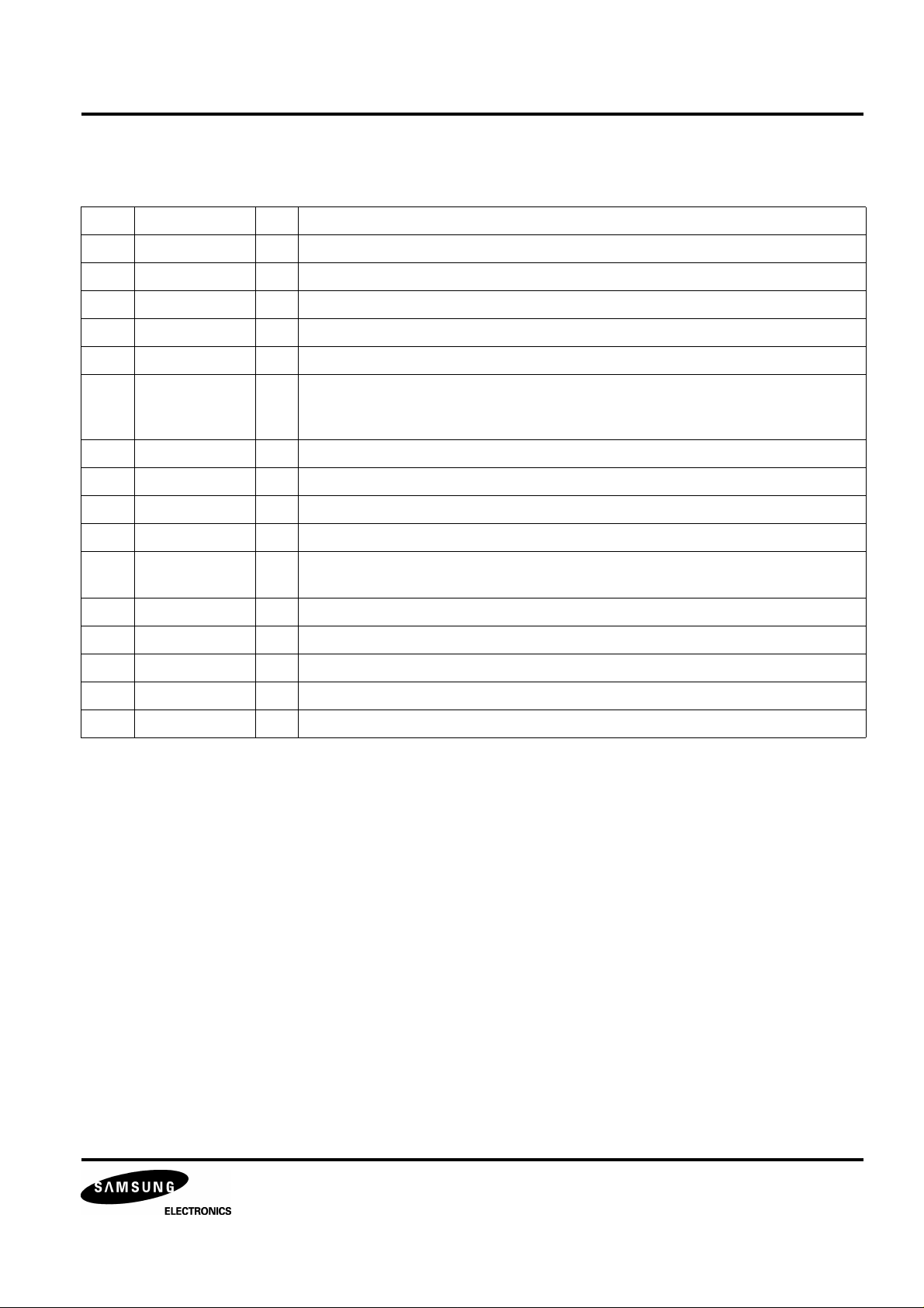
DIGITAL SIGNAL PROCESSOR KS9287
PIN DESCRIPTION (Continued)
No. Pin Name I/O Description
65 TEST1 I TEST input terminal (GND connection)
66 EFMI I EFM signal input
67 DSVO O Digital sum value output
68 /ISTAT O The internal status output
69 TRCNT I Tracking counter input signal
70 LOCK O Output signal of LKFS condition sampled PBFR/16
(if LKFS is "H", LOCK is "H",
if LKFS is sampled "L" at least 8 times by PBFR/16, LOCK is "L")
71 WBCK O Write frame clock (Lock : 7.35 kHz)
72 SMEF O LPF time constant control of the spindle servo error signal
73 SMON O ON/OFF control signal for spindle servo
74 VDD - Digital VDD
75 SMDP O Spindle Motor drive
(Rough control in the SPEED mode, Phase control in the PHASE mode)
76 SMDS O Spindle Motor drive (Velocity control in the PHASE mode)
77 VCOO O VCO output
78 VCOI I VCO input (8.6436MHz when locked by WBCK)
79 DSPEED I Double speed mode select (H: Normal, L: 2 times)
80 APDO O Analog PLL charge pump output
7

DIGITAL SIGNAL PROCESSOR KS9287
ABSOLUTE MAXIMUM RATINGS
Item Symbol Min Typ Max Unit
Supply Voltage V
Input Voltage V
Output Voltage V
Operating Temperature T
Storage Temperature T
DD
I
O
OPR
STG
−0.3 − 7.0 V
−0.3 − 7.0 V
−0.3 − 7.0 V
−20 − 75 °C
−40 − 125 °C
ELECTRICAL CHARACTERISTICS
DC Characteristics (V
= 5 V, V
DD
Item Symbol Condition Min Typ Max Unit Related pins
'H' Input Voltage1 V
'L' Input Voltage1 V
'H' Input Voltage2 V
'L' Input Voltage2 V
'H' Output Voltage1 V
'L' Output Voltage1 V
'H' Output Voltage2 V
'L' Output Voltage2 V
'H' Output Voltage3 V
'L' Output Voltage3 V
Input Leakage Current1 I
Input Leakage Current2 I
IH1
IL1
IH2
IL2
OH1
OL1
OH2
OL2
OH3
OL3
LKG1
LKG2
= 0 V, Ta = 25 °C)
SS
− 0.7V
DD
− − − 0.3V
− 0.8V
DD
− - − 0.2V
IOH=−1mA VDD-0.5 − V
− − V All input
DD
− − V All bi-direction,
DD
DD
IOL=1mA 0 − 0.4 V
IOH=−1mA VDD-0.5 − V
DD
IOL=1mA 0 − 0.4 V
IOH=−1mA VDD-0.5 − V
DD
IOL=1mA 0 − 0.4 V
VI=0~V
VI=0~V
DD
DD
-5 − 5 µA All input
-10 − 10 µA XIN, VCOI
V
MLT, MCK,
V
MDT
V All output pins
V All bi-direction
V All Tri-state
output
(except XIN,
VCOI)
Three State Output
Leakage Current
I
OLKG
VO=0~V
DD
-5 − 5 µA SMEF, SMDP,
SMDS, APDO,
DPDO
8

DIGITAL SIGNAL PROCESSOR KS9287
AC Characteristics
(1) When pulse is input to XI pin (VDD=5V, VSS=0V, Ta=25°C)
Item Symbol Min Typ Max Unit
'H' Level Pulse Width T
WH
'H' Level Pulse Width T
Pulse Frequency T
Input 'H' Level V
Input 'L' Level V
Rising & Falling Time tR,t
t
WH
t
R
WL
CK
IH
IL
13 - - ns
13 - - ns
26 - - ns
VDD-1.0 - - V
- - 0.8 V
F
T
CK
t
F
- - 10 ns
t
WL
V
IH
VIH X 0.9
VDD / 2
VIL X 0.1
V
IL
(2) MCK, MDAT, MLT, TRCNT (VDD=5V, VSS=0V, Ta=25°C)
Item Symbol Min Typ Max Unit
Clock Frequency f
Clock Pulse Width t
Setup Time t
Hold Time t
Delay Time t
Latch Pulse Width t
TRCNT, SQCK Frequency f
TRCNT, SQCK Pulse Width t
CK1
WCK1
SU
H
D
W
CK2
WCK2
- - 1 MHz
500 - - ns
300 - - ns
300 - - ns
300 - - ns
1000 - - ns
- - 1 MHz
500 - - ns
9
 Loading...