

Rockwell Automation 1794-IF4I, 1794-OF4I, 1794-IF2XOF2I, 1794-IF4IXT, 1794-IF4ICFXT User Manual
...Page 1

FLEX I/O Isolated
Analog Modules
1794-IF4I, -OF4I, IF2XOF2I, -IF4IXT,
-IF4ICFXT, -OF4IXT, IF2XOF2IXT
User Manual
Page 2
Important User Information
Solid state equipment has operational characteristics differing from those of
electromechanical equipment. Safety Guidelines for the Application,
Installation and Maintenance of Solid State Controls (publication
SGI-1.1
available from your local Rockwell Automation sales office or online at
http://literature.rockwellautomation.com) describes some important
differences between solid state equipment and hard-wired electromechanical
devices. Because of this difference, and also because of the wide variety of
uses for solid state equipment, all persons responsible for applying this
equipment must satisfy themselves that each intended application of this
equipment is acceptable.
In no event will Rockwell Automation, Inc. be responsible or liable for
indirect or consequential damages resulting from the use or application of
this equipment.
The examples and diagrams in this manual are included solely for illustrative
purposes. Because of the many variables and requirements associated with
any particular installation, Rockwell Automation, Inc. cannot assume
responsibility or liability for actual use based on the examples and diagrams.
No patent liability is assumed by Rockwell Automation, Inc. with respect to
use of information, circuits, equipment, or software described in this manual.
Reproduction of the contents of this manual, in whole or in part, without
written permission of Rockwell Automation, Inc., is prohibited.
Throughout this manual, when necessary, we use notes to make you aware
of safety considerations.
S
WARNING
Identifies information about practices or circumstances that can
cause an explosion in a hazardous environment, which may lead to
personal injury or death, property damage, or economic loss.
IMPORTANT
ATTENTION
Identifies information that is critical for successful application and
understanding of the product.
Identifies information about practices or circumstances that can
lead to: personal injury or death, property damage, or economic
loss. Attentions help you identify a hazard, avoid a hazard, and
recognize the consequence.
SHOCK HAZARD
Labels may be on or inside the equipment, such as a drive or motor,
to alert people that dangerous voltage may be present.
BURN HAZARD
Labels may be on or inside the equipment, such as a drive or motor,
to alert people that surfaces may reach dangerous temperatures.
Rockwell Automation, Allen-Bradley, FLEX, RSNetWorx, RSLogix5000, and TechConnect are trademarks of Rockwell Automation,
Inc.
Trademarks not belonging to Rockwell Automation are property of their respective companies.
Page 3

Using this Manual
Preface
Purpose of this Manual
Audience
Vocabulary
This manual shows you how to use your FLEX I/O Isolated Analog
modules with Allen-Bradley programmable controllers. The manual
helps you install, program and troubleshoot your modules.
Except where noted, information that applies to 1794-IF4I, 1794-OF4I,
and IF2XOF2I also applies to 1794-IF4IXT, 1794-IF4ICFXT,
1794-OF4IXT, and IF2XOF2IXT.
You must be able to program and operate an Allen-Bradley
programmable controller to make efficient use of your FLEX I/O
modules. In particular, you must know how to program block
transfers.
We assume that you know how to do this in this manual. If you do
not, refer to the appropriate programming and operations manual
before you attempt to program your modules.
In this manual, we refer to:
• the isolated analog input or isolated analog output module as
the “input module” or ‘‘output module”
• the Programmable Controller as the “controller”
Manual Organization
3 Publication 1794-6.5.8 - January 2010
This manual is divided into five chapters. The following chart lists
each chapter with its corresponding title and a brief overview of the
topics covered in that chapter.
Section Title Contents
Chapter 1 Overview of FLEX I/O and
your Analog Modules
Chapter 2 How to Install Your Analog
Module
Chapter 3 Module Programming Explains block transfer
Describes FLEX I/O Isolated
Analog modules, features,
and how they function
How to install and wire the
modules
programming, sample
programs
Page 4

Preface 4
Section Title Contents
Chapter 4 Writing Configuration to and
Reading Status from Your
Module with a Remote I/O
Adapter
Chapter 5 Communication and I/O
Image Table Mapping with
the DeviceNet/ControlNet
Adapter
Chapter 6 Input, Output, Status and
Configuration Files for
Analog Modules when used
with ControlNet
Chapter 7 Calibrating Your Module Explains how to calibrate
Appendix A Specifications Specifications for the
Appendix B Class I, Division 2, Group A,
B, C, D Hazardous Locations
Statement
Explains how to configure
your modules and read
status information from your
modules when using a
remote I/O adapter
Explains how you
communicate with your
modules, and how the I/O
image is mapped when
using a DeviceNet adapter
Explains how you
communicate with your
modules over ControlNet.
your module.
isolated analog modules
Hazardous location approval
Common Techniques Used in this Manual
For Additional Information
Catalog Numbers Voltage Description Publications
1794 1794 FLEX I/O Product Data 1794-2.1
1794-ACN 24V dc ControlNet Adapter 1794-5.8
1794-ACNR 24V dc Redundant Media ControlNet Adapter 1794-5.18
1794-ADN 24V dc DeviceNet Adapter 1794-5.14 1794-6.5.5
1794-ASB/C 24V dc Remote I/O Adapter 1794-5.46 1794-6.5.9
The following conventions are used throughout this manual:
• Bulleted lists such as this one provide information, not
procedural steps.
• Numbered lists provide sequential steps or hierarchical
information.
For additional information on FLEX I/O systems and modules, refer to
the following documents:
Installation
Instructions
User Manual
Publication 1794-6.5.8 - January 2010
Page 5

Catalog Numbers Voltage Description Publications
Preface 5
Installation
Instructions
1794-ASB2 24V dc 2-Slot Remote I/O Adapter 1794-5.44 1794-6.5.3
1794-TB2
1794-TB3
1794-TBN Terminal Base Unit 1794-5.16
1794-TBNF Fused Terminal Base Unit 1794-5.17
1794-TB3T Temperature Terminal Base Unit 1794-5.41
1794-TB3S Spring Clamp Terminal Base Unit 1794-5.42
1794-TB3TS Spring Clamp Temperature Terminal Base
1794-IB16 24V dc 16 Sink Input Module 1794-5.4
1794-OB16 24V dc 16 Source Output Module 1794-5.3
1794-IV16 24V dc 16 Source Input Module 1794-5.28
1794-OV16 24V dc 16 Sink Output Module 1794-5.29
1794-OB8EP 24V dc 8 Electronically Fused Output Module 1794-5.20
1794-OW8 24V dc 8 Output Relay Module 1794-5.19
1794-IB10XOB6 24V dc 10 Input/6 Output Module 1794-5.24
1794-IE8 24V dc Selectable Analog 8 Input Module 1794-5.6
1794-OE4 24V dc Selectable Analog 4 Output Module 1794-5.5 1794-6.5.2
1794-IE4XOE2 24V dc 4 Input/2 Output Analog Module 1794-5.15
2-wire Terminal Base
3-wire Terminal Base
Unit
1794-5.2
1794-5.43
User Manual
Summary
1794-IR8 24V dc 8 RTD Input Analog Module 1794-5.22 1794-6.5.4
1794-IT8 24V dc 8 Thermocouple Input Module 1794-5.21 1794-6.5.7
1794-IB8S 24V dc Sensor Input Module 1794-5.7
1794-IA8 120V ac 8 Input Module 1794-5.9
1794-OA8 120V ac Output Module 1794-5.10
1794-CE1, -CE3 Extender Cables 1794-5.12
1794-NM1 Mounting Kit 1794-5.13
1794-PS1 24V dc Power Supply 1794-5.35
1794-PS13 24V dc Power Supply 1794-5.69
This preface gave you information on how to use this manual
efficiently. The next chapter introduces you to the remote I/O adapter
module.
Publication 1794-6.5.8 - January 2010
Page 6

Preface 6
Publication 1794-6.5.8 - January 2010
Page 7

Important User Information . . . . . . . . . . . . . . . . . . . . . . . . . . 2
Preface
Using this Manual . . . . . . . . . . . . . . . . . . . . . . . . . . . . . . 3
Purpose of this Manual . . . . . . . . . . . . . . . . . . . . . . . . . . . . . 3
Audience . . . . . . . . . . . . . . . . . . . . . . . . . . . . . . . . . . . . . . . 3
Vocabulary . . . . . . . . . . . . . . . . . . . . . . . . . . . . . . . . . . . . . . 3
Manual Organization. . . . . . . . . . . . . . . . . . . . . . . . . . . . . . . 3
Common Techniques Used in this Manual . . . . . . . . . . . . . . . 4
For Additional Information . . . . . . . . . . . . . . . . . . . . . . . . . . 4
Summary . . . . . . . . . . . . . . . . . . . . . . . . . . . . . . . . . . . . . . . 5
Table of Contents Chapter
Overview of FLEX I/O and your
Analog Modules
Chapter Objectives . . . . . . . . . . . . . . . . . . . . . . . . . . . . . . . 11
The FLEX I/O System . . . . . . . . . . . . . . . . . . . . . . . . . . . . . 11
Types of FLEX I/O Modules . . . . . . . . . . . . . . . . . . . . . . . . 12
How FLEX I/O Analog Modules Communicate with
Programmable Controllers . . . . . . . . . . . . . . . . . . . . . . . . . . 13
Features of Your Analog Modules . . . . . . . . . . . . . . . . . . . . 14
Summary . . . . . . . . . . . . . . . . . . . . . . . . . . . . . . . . . . . . . . 14
Chapter
How to Install Your Analog
Module
Chapter Objectives . . . . . . . . . . . . . . . . . . . . . . . . . . . . . . . 15
Before You Install Your Analog Module. . . . . . . . . . . . . . . . 15
Compliance to European Union Directives . . . . . . . . . . . . . . 15
EMC Directive . . . . . . . . . . . . . . . . . . . . . . . . . . . . . . . . 15
Low Voltage Directive (to be confirmed). . . . . . . . . . . . . 16
Power Requirements . . . . . . . . . . . . . . . . . . . . . . . . . . . . . . 16
Installing the Module. . . . . . . . . . . . . . . . . . . . . . . . . . . . . . 18
Mounting the Terminal Base Unit on a DIN Rail . . . . . . . 18
Panel/Wall Mounting . . . . . . . . . . . . . . . . . . . . . . . . . . . 20
Mounting the Analog Module on the Terminal Base Unit. 22
Connecting Wiring for the Analog Modules . . . . . . . . . . . . . 23
Connecting Wiring using a 1794-TB3, -TB3T, -TB3S or -TB3TS
Terminal Base Unit . . . . . . . . . . . . . . . . . . . . . . . . . . . . 24
Wiring to a 1794-TBN or 1794-TBNF Terminal Base Unit . 26
Module Indicators . . . . . . . . . . . . . . . . . . . . . . . . . . . . . . . . 30
Chapter Summary . . . . . . . . . . . . . . . . . . . . . . . . . . . . . . . . 30
Table of Contents
Chapter
Module Programming
7 Publication 1794-6.5.8 - January 2010
Chapter Objectives . . . . . . . . . . . . . . . . . . . . . . . . . . . . . . . 31
Block Transfer Programming . . . . . . . . . . . . . . . . . . . . . . . . 31
Configuration Rungs . . . . . . . . . . . . . . . . . . . . . . . . . . . . . . 32
Example Configuration Rungs. . . . . . . . . . . . . . . . . . . . . 32
Sample Programs for FLEX I/O Analog Modules. . . . . . . . . . 33
PLC-3 Programming . . . . . . . . . . . . . . . . . . . . . . . . . . . . 33
PLC-5 Programming . . . . . . . . . . . . . . . . . . . . . . . . . . . . 35
PLC-2 Programming . . . . . . . . . . . . . . . . . . . . . . . . . . . . 38
SLC-5 Programming. . . . . . . . . . . . . . . . . . . . . . . . . . . . . . . 38
Page 8

Table of Contents 8
Writing Configuration to and
Reading Status from Your Module
with a Remote I/O Adapter
Chapter Summary . . . . . . . . . . . . . . . . . . . . . . . . . . . . . . . . 51
Chapter
Chapter Objectives . . . . . . . . . . . . . . . . . . . . . . . . . . . . . . . 53
Configuring Your Analog Module . . . . . . . . . . . . . . . . . . . . 53
Range Selection . . . . . . . . . . . . . . . . . . . . . . . . . . . . . . . . . 54
Safe State Selection . . . . . . . . . . . . . . . . . . . . . . . . . . . . . . . 54
Data Format . . . . . . . . . . . . . . . . . . . . . . . . . . . . . . . . . . . . 54
Real Time Sampling . . . . . . . . . . . . . . . . . . . . . . . . . . . . . . 55
Input Filtering. . . . . . . . . . . . . . . . . . . . . . . . . . . . . . . . . . . 56
Reading Data From Your Module. . . . . . . . . . . . . . . . . . . . . 57
Mapping Data for the Analog Modules. . . . . . . . . . . . . . . . . 57
8 Input Analog Module (Cat. No. 1794-IF4I) . . . . . . . . . . 58
4 Isolated Output Analog Module (Cat. No. 1794-OF4I) . . 64
2 Input/2 Output Analog Combo Module (Cat. No.
1794-IF2XOF2I) . . . . . . . . . . . . . . . . . . . . . . . . . . . . . . . 69
Chapter Summary . . . . . . . . . . . . . . . . . . . . . . . . . . . . . . . . 76
Communication and I/O Image
Table Mapping with the
DeviceNet/ControlNet Adapter
Input, Output, Status and
Configuration Files for Analog
Modules when used with
ControlNet
Chapter
Chapter Objectives . . . . . . . . . . . . . . . . . . . . . . . . . . . . . . . 77
About RSNetWorx and RSLogix . . . . . . . . . . . . . . . . . . . . . . 77
Polled I/O Structure . . . . . . . . . . . . . . . . . . . . . . . . . . . . . . 77
Adapter Input Status Word . . . . . . . . . . . . . . . . . . . . . . . 78
Mapping Data into the Image Table. . . . . . . . . . . . . . . . . . . 79
4 Input Isolated Analog Module (Cat. No. 1794-IF4I) Image
Table Mapping . . . . . . . . . . . . . . . . . . . . . . . . . . . . . . . 79
4 Output Isolated Analog Module (Cat. No. 1794-OF4I) Image
Table Mapping . . . . . . . . . . . . . . . . . . . . . . . . . . . . . . . 86
Isolated Analog Combo Module (Cat. No. 1794-IF2XOF2I
Series B) Image Table Mapping . . . . . . . . . . . . . . . . . . . 91
Defaults . . . . . . . . . . . . . . . . . . . . . . . . . . . . . . . . . . . . . . . 97
Chapter
Chapter Objectives . . . . . . . . . . . . . . . . . . . . . . . . . . . . . . . 99
About the ControlNet Adapter . . . . . . . . . . . . . . . . . . . . . . . 99
Commun ication Over the FLEX I/O Backplane . . . . . . . . . . 99
Polled I/O Structure . . . . . . . . . . . . . . . . . . . . . . . . . . . . . 100
Adapter Input Status Word . . . . . . . . . . . . . . . . . . . . . . 101
Safe State Data . . . . . . . . . . . . . . . . . . . . . . . . . . . . . . . . . 102
Communication Fault Behavior . . . . . . . . . . . . . . . . . . . . . 102
Idle State Behavior . . . . . . . . . . . . . . . . . . . . . . . . . . . . . . 102
Input Data Behavior Upon Module Removal . . . . . . . . . . . 103
4 Input Isolated Analog Module (Cat. No. 1794-IF4I) Image
Table Mapping . . . . . . . . . . . . . . . . . . . . . . . . . . . . . . 103
Publication 1794-6.5.8 - January 2010
Page 9

Calibrating Your Module
Table of Contents 9
4 Output Isolated Analog Module (Cat. No. 1794-OF4I) Image
Table Mapping . . . . . . . . . . . . . . . . . . . . . . . . . . . . . . 108
Isolated Analog Combo Module (Cat. No. 1794-IF2XOF2I)
Image Table Mapping . . . . . . . . . . . . . . . . . . . . . . . . . 113
Chapter
Chapter Objective . . . . . . . . . . . . . . . . . . . . . . . . . . . . . . . 119
When and How to Calibrate Your Isolated Analog Module . 119
Tools and Equipment . . . . . . . . . . . . . . . . . . . . . . . . . . . . 120
Calibrating Your Isolated Analog Input Module . . . . . . . . . 121
Bits Used During Calibration . . . . . . . . . . . . . . . . . . . . 121
Offset Calibration for Inputs . . . . . . . . . . . . . . . . . . . . . 122
Setting the Input Gain . . . . . . . . . . . . . . . . . . . . . . . . . 124
Calibrating Your Isolated Analog Output Module . . . . . . . . 125
Bits Used During Calibration . . . . . . . . . . . . . . . . . . . . 125
Calibrating Voltage Outputs . . . . . . . . . . . . . . . . . . . . . 126
Offset Calibration for Voltage Outputs 126
Gain Calibration for Outputs 127
Calibrating Current Outputs . . . . . . . . . . . . . . . . . . . . . 128
Gain Calibration for Current Outputs 128
Offset Calibration for Current Outputs 128
Final Gain Calibration for Current Inputs 130
Scaling Inputs . . . . . . . . . . . . . . . . . . . . . . . . . . . . . . . 131
Scaling Outputs . . . . . . . . . . . . . . . . . . . . . . . . . . . . . . 132
Chapter Summary . . . . . . . . . . . . . . . . . . . . . . . . . . . . . . . 132
Specifications
Class I, Division 2, Group A, B, C, D
Hazardous Locations Statement
Index
Appendix
Filter Response for 150Hz, 300Hz and 600Hz Conversion 134
Appendix
Publication 1794-6.5.8 - January 2010
Page 10

Table of Contents 10
Publication 1794-6.5.8 - January 2010
Page 11
Chapter
Overview of FLEX I/O and your Analog Modules
1
Chapter Objectives
The FLEX I/O System
Adapter Terminal Base I/O Module
In this chapter, we tell you about:
• what the FLEX I/O system is and what it contains
• types of FLEX I/O analog modules
• how FLEX I/O analog modules communicate with
programmable controllers
• the features of your analog modules
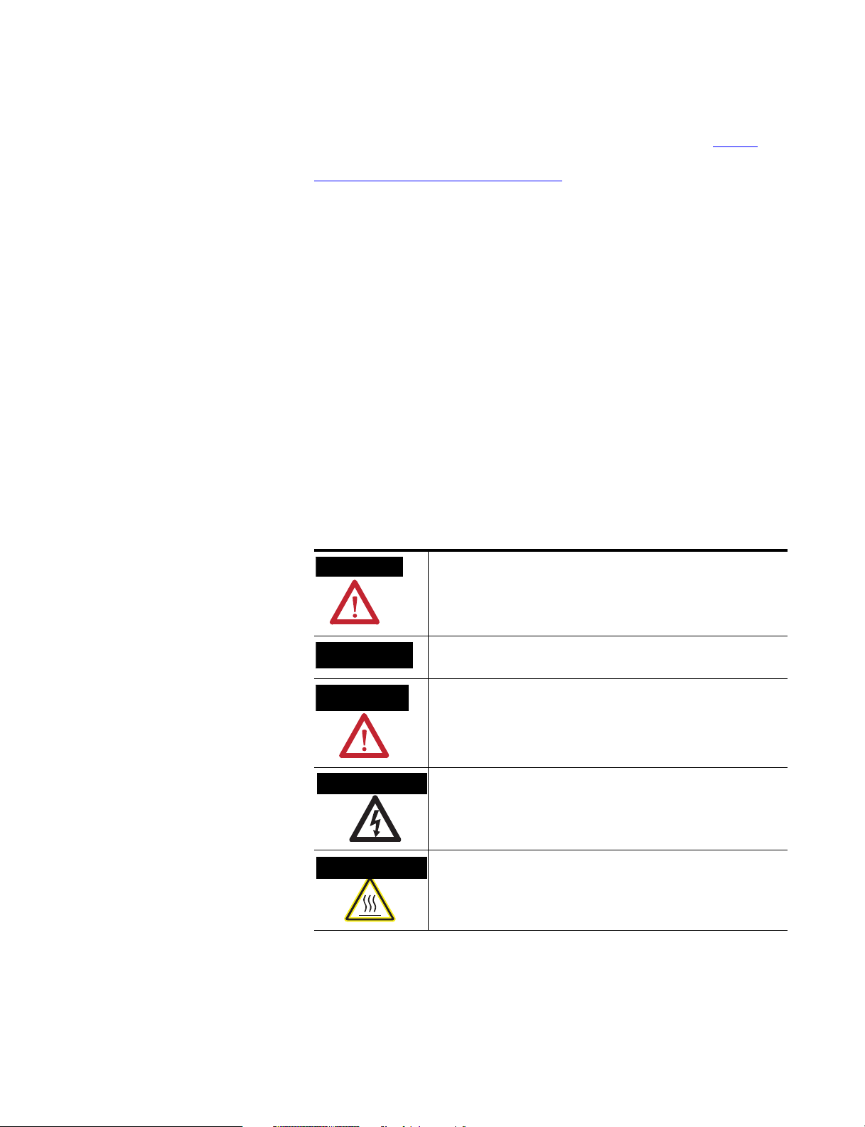
FLEX I/O is a small, modular I/O system for distributed applications
that performs all of the functions of rack-based I/O. The FLEX I/O
system contains the following components shown in
Figure 1.1
Figure 1.1:
I
V
I
V
I
V
I
V
I
V
5
I
V
20125
• adapter/power supply – powers the internal logic for as many as
eight I/O modules
• terminal base – contains a terminal strip to terminate wiring for
two- or three-wire devices
• I/O module – contains the bus interface and circuitry needed to
perform specific functions related to your application
11 Publication 1794-6.5.8 - January 2010
Page 12

12 Overview of FLEX I/O and your Analog Modules
Types of FLEX I/O Modules
Catalog Number Voltage Inputs Outputs Description
1794-IF4I 24V dc 4 – analog – 4 input, isolated
1794-OF4I 24V dc – 4 analog – 4 output, isolated
1794-IF2XOF2I 24V dc 2 2 analog – 2 input, isolated and 2 output, isolated
We describe the following FLEX I/O Analog modules in this user manual:
FLEX I/O analog input, output and combination modules are block
transfer modules that interface analog signals with any Allen-Bradley
programmable controllers that have block transfer capability. Block
transfer programming moves input from the module’s memory to a
designated area in the processor data table, and output data words
from a designated area in the processor data table to the module’s
memory. Block transfer programming also moves configuration words
from the processor data table to module memory.
The analog modules have selectable ranges as shown in the table
below:
Input Values Data Format Underrange/Overrange
4–20mA signed 2’s complement 4% Underrange, 4% Overrange
±10V signed 2’s complement 2% Underrange, 2% Overrange
±5V signed 2’s complement 4% Underrange, 4% Overrange
0–20mA signed 2’s complement % 0% Underrange, 4% Overrange
4-20mA signed 2’s complement % 4% Underrange, 4% Overrange
0–10V signed 2’s complement % 0% Underrange, 2% Overrange
±10V signed 2’s complement % 2% Underrange, 2% Overrange
0–20mA binary 0% Underrange, 4% Overrange
4–20mA binary 4% Underrange, 4% Overrange
0–10V binary 0% Underrange, 2% Overrange
0–5V binary 0% Underrange, 4% Overrange
±20mA offset binary, 8000H = 0mA 4% Underrange, 4% Overrange
4–20mA offset binary, 8000H = 4mA 4% Underrange, 4% Overrange
±10V offset binary, 8000H = 0V 2% Underrange, 2% Overrange
±5V offset binary, 8000H = 0V 4% Underrange, 4% Overrange
Publication 1794-6.5.8 - January 2010
Page 13
Overview of FLEX I/O and your Analog Modules 13
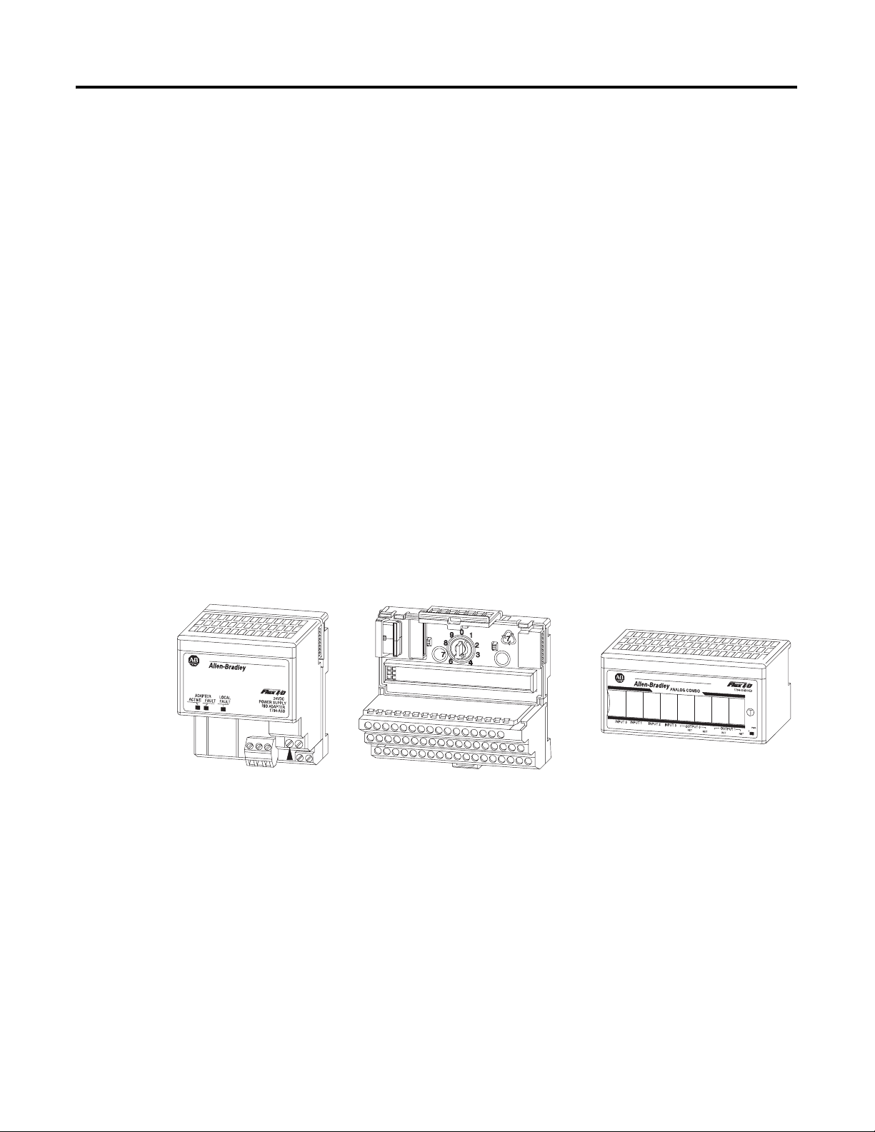
How FLEX I/O Analog Modules Communicate with Programmable Controllers
The adapter transfers your configuration data
to the module using a BTW.
Allen-Bradley
ADAPTER
ACTIVE FAULT
LOCAL
FAULT
POWER SUPPLY
RIO ADAPTER
1794-ASB
24VDC
The adapter/power supply transfers data to the module (block transfer
write) and from the module (block transfer read) using BTW and BTR
instructions in your ladder diagram program. These instructions let the
adapter obtain input values and status from the module, and let you
send output values and establish the module’s mode of operation.
Figure 1.2 describes the communication process.
Figure 1.2
An Example of Communication Between an Adapter and an Analog Input Module
1
Flexbus
4
Your ladder program instructs the
adapter to perform a BTR of the values
and stores them in a data table.
5
The adapter and module determine
that the transfer was made without error
and input values are within specified
range.
Allen-Bradley
ANALOG INPUT
INPUT 0INPUT 2 INPUT 4 INPUT 6INPUT 1 INPUT 3 INPUT 5 INPUT 7
VI VI VI VI VI VI VI V
I
External devices transmit
analog signals to the module.
1794±IE8
The module converts analog signals
into integer format and stores these
values until the adapter requests their
transfer.
2
2
3
6
Your ladder program can use and/or move the data (if valid)
before it is written over by the transfer of new data in a
subsequent transfer.
7
Your ladder program performs BTWs to the module when you power
it up, and any time you wish to reconfigure the module.
Publication 1794-6.5.8 - January 2010
Page 14
14 Overview of FLEX I/O and your Analog Modules
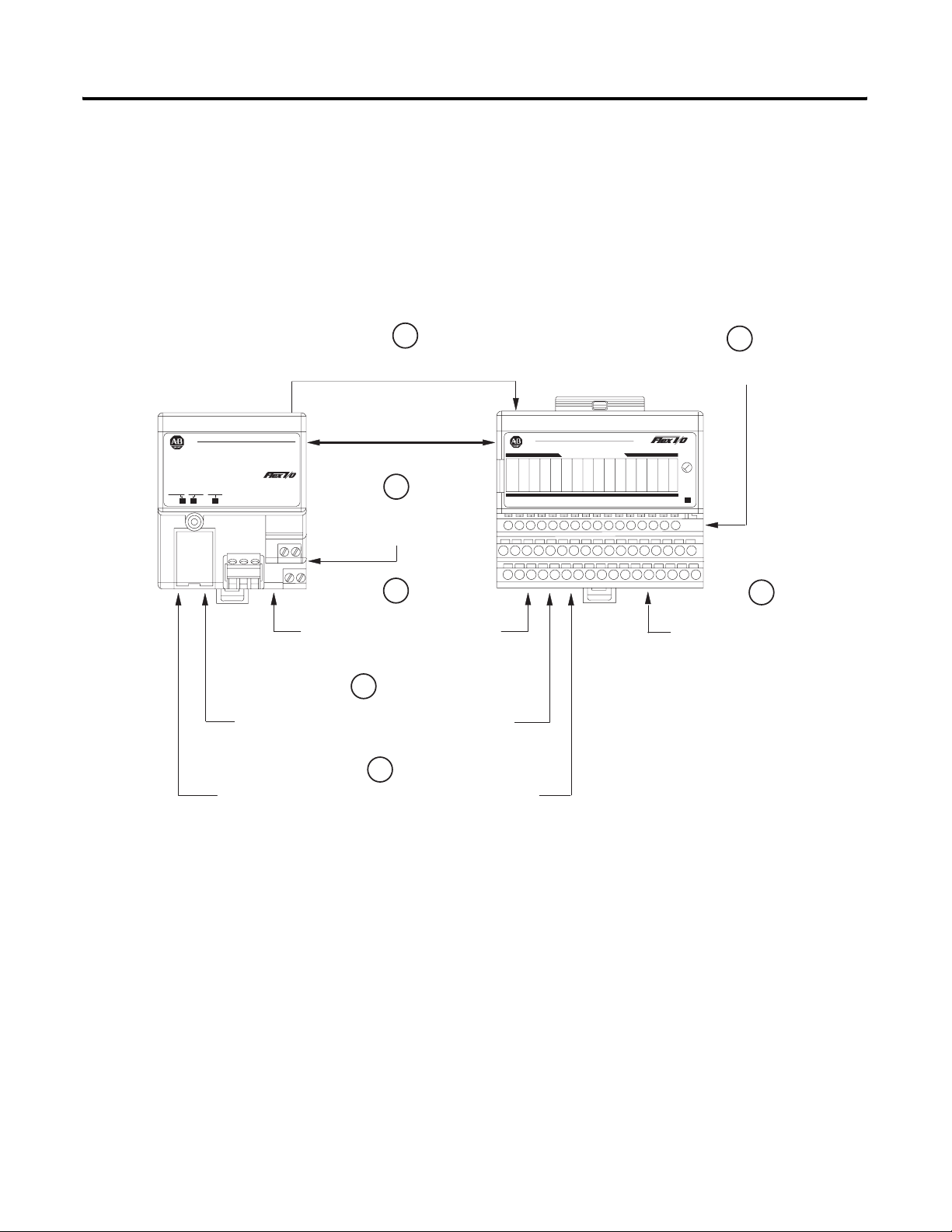
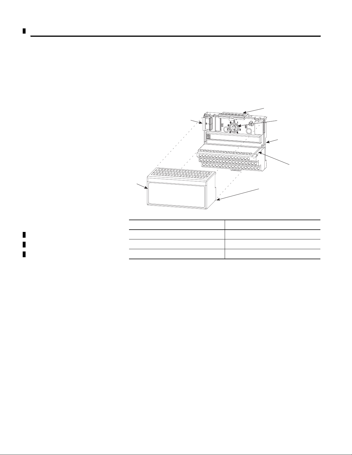
Features of Your Analog Modules
Each module has a unique label identifying its keyswitch position,
wiring and module type. A removable label provides space for writing
individual designations per your application.
1794-IF4I
Module Type
Removable
Label
Keyswitch
Position
Indicator (#3)
Input Designators
1794-OF4I
Output Designators
Green Power/Status
Indicator
Module Type
Removable
Label
Keyswitch
Position
Indicator (#4)
Green Power/Status
Indicator
Summary
1794-IF2XOF2I
Module Type
Removable
Label
Keyswitch
Position
Indicator (#5)
Input and Output Designators
Green Power/Status
Indicator
In this chapter you learned about the FLEX I/O system and the types
of analog modules and how they communicate with programmable
controllers.
Publication 1794-6.5.8 - January 2010
Page 15

How to Install Your Analog Module
Chapter
2
Chapter Objectives
Before You Install Your Analog Module
Compliance to European Union Directives
In this chapter, we tell you about:
• how to install your module
• how to set the module keyswitch
• how to wire the terminal base
• the indicators
Before installing your analog module in the I/O chassis:
You need to: As described under:
Calculate the power requirements of all
modules in each chassis.
Position the keyswitch on the terminal base Mounting the Analog Module on the
If this product has the CE mark it is approved for installation within
the European Union and EEA regions. It has been designed and tested
to meet the following directives.
Power Requirements, page 2-16
Terminal Base Unit, page 2-22
EMC Directive
This product is tested to meet Council Directive 2004/10/EC
Electromagnetic Compatibility (EMC) and the following standards, in
whole or in part, documented in a technical construction file:
• European Union 2004/108/EC EMC Directive, compliant with:
EN 61326-1; Meas./Control/Lab., Industrial Requirements
EN 61000-6-2; Industrial Immunity
EN 61000-6-4; Industrial Emissions
EN 61131-2; Programmable Controllers (Clause 8, Zone A & B)
• European Union 2006/95/EC LVD, compliant with:
EN 61131-2; Programmable Controllers (Clause 11)
This product is intended for use in an industrial environment.
15 Publication 1794-6.5.8 - January 2010
Page 16

16 How to Install Your Analog Module
Low Voltage Directive
This product is tested to meet Council Directive 2006/95/EC Low
Voltage, by applying the safety requirements of EN 61131–2
Programmable Controllers, Part 2 – Equipment Requirements and
Tests.
For specific information required by EN 61131-2, see the appropriate
sections in this publication, as well as the following Allen-Bradley
publications:
• Industrial Automation Wiring and Grounding Guidelines For
Noise Immunity, publication 1770-4.1
• Guidelines for Handling Lithium Batteries, publication AG-5.4
• Automation Systems Catalog, publication B111
Open style devices must be provided with environmental and safety
protection by proper mounting in enclosures designed for specific
application conditions. See NEMA Standards publication 250 and IEC
publication 529, as applicable, for explanations of the degrees of
protection provided by different types of enclosure.
Power Requirements
The wiring of the terminal base unit is determined by the current draw
through the terminal base. Make certain that the current draw does
not exceed 10A.
ATTENTION
Total current draw through the terminal base unit is
limited to 10A. Separate power connections may be
necessary.
Publication 1794-6.5.8 - January 2010
Page 17
How to Install Your Analog Module 17
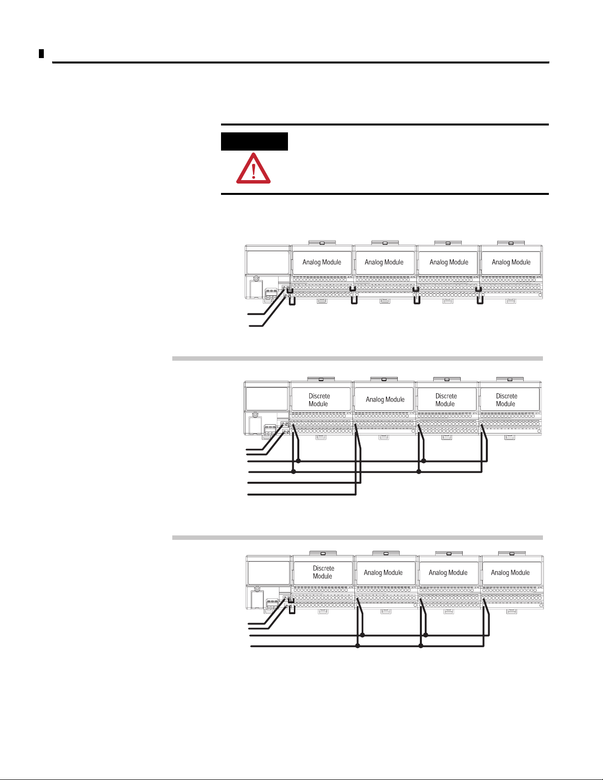
Methods of wiring the terminal base units are shown in the illustration
below.
Daisy-chaining
Individual
ATTENTION
24V dc
Do not daisy chain power or ground from an analog
terminal base unit to any ac or dc discrete module
terminal base unit.
Note: All modules must be analog modules for this configuration.
Wiring
when total current draw is less than 10A
Combination
24V dc
24V dc or
120V ac
24V dc
24V dc
24V dc
Analog module wiring separate from discrete wiring.
W
iring when total current draw is greater than 10A
Note: All modules powered by the same power supply
must be analog modules for this configuration.
T
otal current draw through any base unit must not be greater than 10A
Note: Use this configuration if using any
ªnoisyº dc discrete I/O modules in your system.
Publication 1794-6.5.8 - January 2010
Page 18
18 How to Install Your Analog Module
Installing the Module
Installation of the analog module consists of:
• mounting the terminal base unit
• installing the analog module into the terminal base unit
• installing the connecting wiring to the terminal base unit
If you are installing your module into a terminal base unit that is
already installed, proceed to
Mounting the Analog Module on the
Terminal Base Unit on page 2-22.
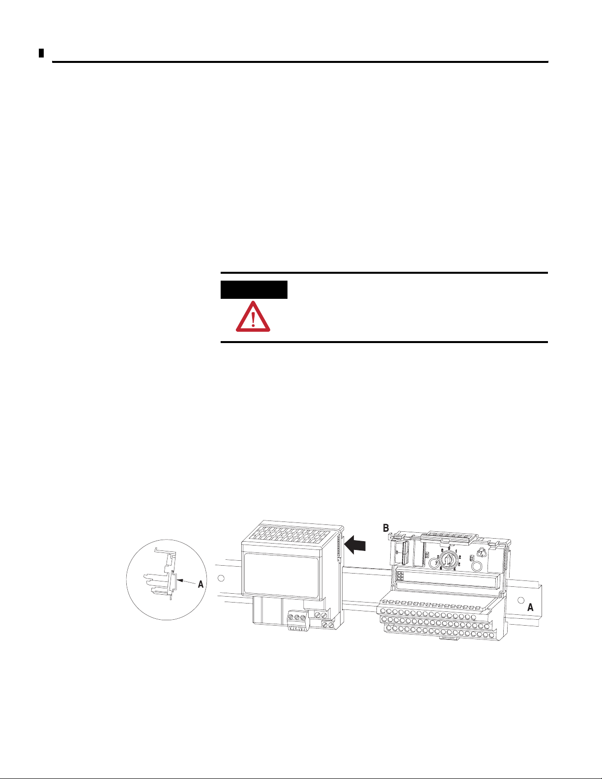
Mounting the Terminal Base Unit on a DIN Rail
ATTENTION
1. Remove the cover plug (if used) in the male connector of the
unit to which you are connecting this terminal base unit.
Do not remove or replace a terminal base unit when
power is applied. Interruption of the flexbus can
result in unintended operation or machine motion.
2. Check to make sure that the 16 pins in the male connector on
the adjacent device are straight and in line so that the mating
female connector on this terminal base unit will mate correctly.
3. Position the terminal base on the 35 x 7.5mm DIN rail A (A-B pt.
no. 199-DR1; 46277-3; EN 50022) at a slight angle with hook B
on the left side of the terminal base hooked into the right side of
the unit on the left. Proceed as follows:
Figure 2.1
Position terminal base at a slight angle and hooked over the
top of the DIN rail.
Publication 1794-6.5.8 - January 2010
Page 19
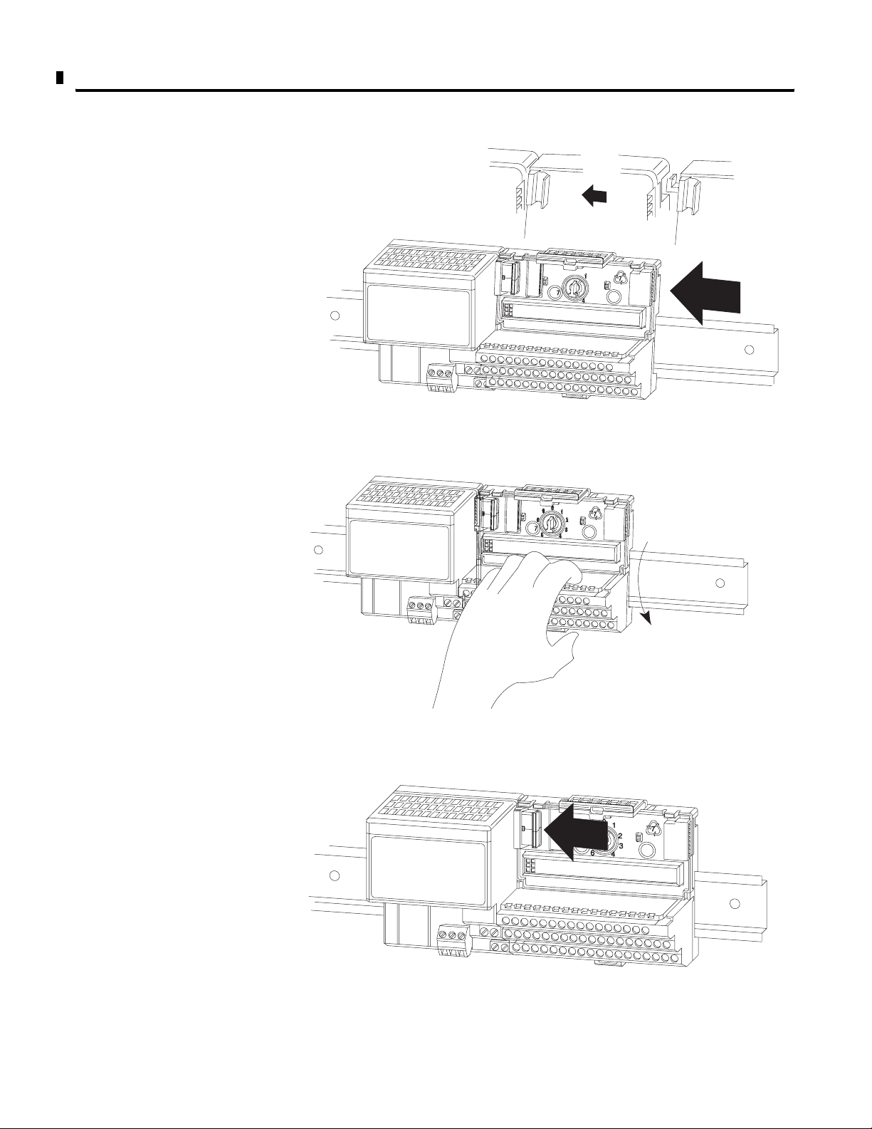
Figure 2.2
How to Install Your Analog Module 19
Slide the terminal base unit over tight against the adapter.
Make sure the hook on the terminal base slides under the edge of
the adapter and the flexbus connector is fully retracted.
Press down on the terminal base unit to lock the terminal base
on the DIN rail. If the terminal base does not lock into place,
use a screwdriver or similar device to open the locking tab,
press down on the terminal base until flush with the DIN rail
and release the locking tab to lock the base in place.
Gently push the flexbus connector into the side
of the adapter to complete the backplane connection.
4. Repeat steps 1 - 3 to install the next terminal base.
Publication 1794-6.5.8 - January 2010
30077-M
Page 20
20 How to Install Your Analog Module
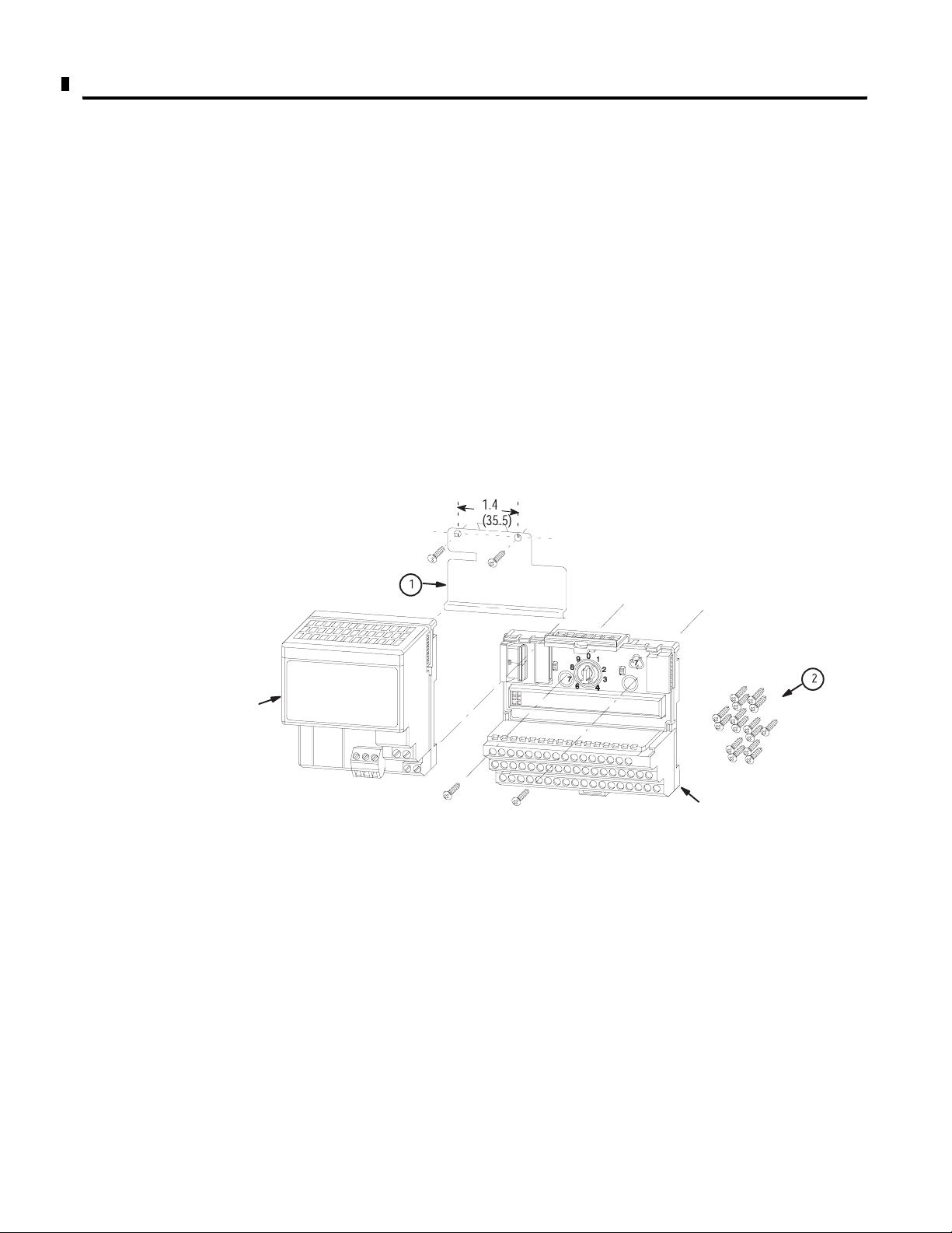
Panel/Wall Mounting
Installation on a wall or panel consists of:
• laying out the drilling points on the wall or panel
• drilling the pilot holes for the mounting screws
• mounting the adapter mounting plate
• installing the terminal base units and securing them to the wall
or panel
If you are installing your module into a terminal base unit that is
already installed, proceed to “Mounting the Analog Module on the
Terminal Base” on .
Use the mounting kit Cat. No. 1794-NM1 for panel/wall mounting.
1794-NM1
1 ± Mounting Plate for Adapter
2 ± 18 #6 self-tapping screws
(2 for the adapter, and 2
each for up to 8 modules)
Mounting Kit
Contents:
Adapter Module
(not included)
Terminal Base Unit
(not included)
Publication 1794-6.5.8 - January 2010
Page 21
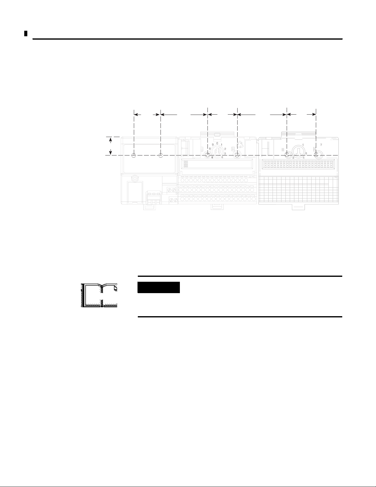
How to Install Your Analog Module 21
To install the mounting plate on a wall or panel:
1. Lay out the required points on the wall/panel as shown in the
drilling dimension drawing.
Figure 2.3 Drilling Dimensions for Panel/Wall Mounting of FLEX I/O
Inches
(Millimeters)
.83 (21)
More
1.4
(35.5)
2.3
(58.5)
1.4
(35.5)
2.3
(58.5)
1.4
(35.5)
2. Drill the necessary holes for the #6 self-tapping mounting
screws.
3. Mount the mounting plate (1) for the adapter module using two
#6 self-tapping screws (18 included for mounting up to 8
modules and the adapter).
IMPORTANT
Make certain that the mounting plate is properly
grounded to the panel. Refer to “Industrial
Automation Wiring and Grounding Guidelines,”
publication 1770-4.1.
4. Hold the adapter (2) at a slight angle and engage the top of the
mounting plate in the indention on the rear of the adapter
module.
5. Press the adapter down flush with the panel until the locking
lever locks.
6. Position the terminal base unit up against the adapter and push
the female bus connector into the adapter.
7. Secure to the wall with two #6 self-tapping screws.
8. Repeat for each remaining terminal base unit.
The adapter is capable of addressing eight modules. Do not
exceed a maximum of eight terminal base units in your system.
Publication 1794-6.5.8 - January 2010
Page 22
22 How to Install Your Analog Module
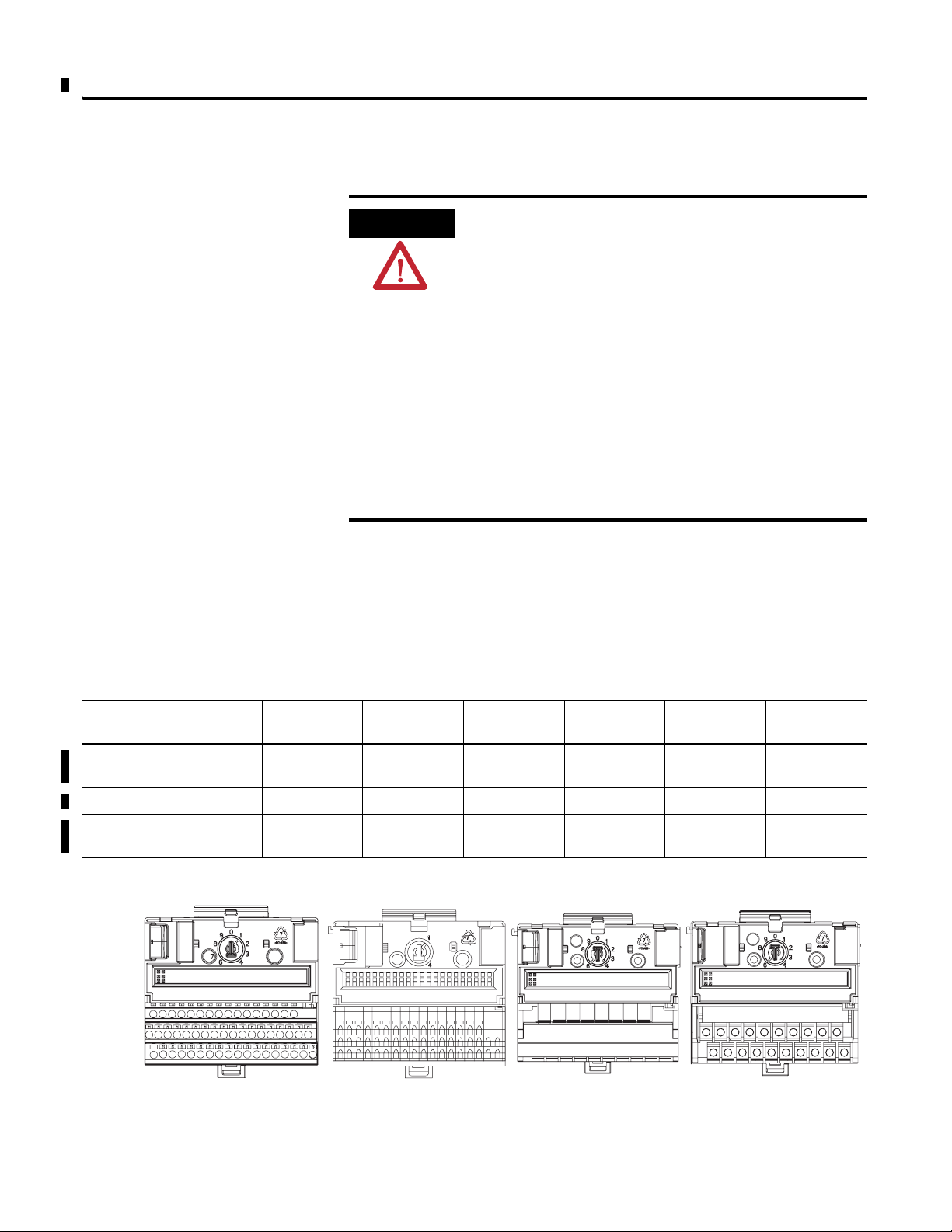
Mounting the Analog Module on the Terminal Base Unit
1. Rotate the keyswitch (1) on the terminal base unit (2) clockwise
to the position required for the specific type of analog module.
Figure 2.4
7
3
1
2
6
4
Analog Module Catalog Number Keyswitch Position
1794-IF4I, 1794-IF4IXT, 1794-IF4ICFXT 3
1794-OF4I, 1794-OF4IXT 4
1794-IF2XOF2I, 1794-IF2XOF2IXT 5
5
2. Make certain the flexbus connector (3) is pushed all the way to
the left to connect with the neighboring terminal base/adapter.
You cannot install the module unless the connector is fully
extended.
3. Make sure that the pins on the bottom of the module are straight
so they will align properly with the connector in the terminal
base unit.
4. Position the module (4) with its alignment bar (5) aligned with
the groove (6) on the terminal base.
Publication 1794-6.5.8 - January 2010
5. Press firmly and evenly to seat the module in the terminal base
unit. The module is seated when the latching mechanism (7) is
locked into the module.
Page 23
How to Install Your Analog Module 23
6. Repeat the above steps to install the next module in its terminal
base unit.
Connecting Wiring for the Analog Modules
ATTENTION
Remove field-side power before removing or
inserting the module. This module is designed so
you can remove and insert it under backplane
power. When you remove or insert a module with
field-side power applied, an electrical arc may occur.
An electrical arc can cause personal injury or
property damage by:
• sending an erroneous signal to your system’s field
devices causing unintended machine motion
• causing an explosion in a hazardous environment
Repeated electrical arcing causes excessive wear to
contacts on both the module and its mating
connector. Worn contacts may create electrical
resistance.
Wiring to the analog modules is made through the terminal base unit
on which the module mounts.
Refer to the following table for recommended terminal base units that
you can use for each module.
Module 1794-TB3 1794-TBT 1794-TB3S 1794-TB3TS 1794-TB3S 1794-TBN,
-TBNF
1794-IF4I, 1794-IF4IXT,
1794-IF4ICFXT
1794-OF4I, 1794-OF4IXT Yes Yes Yes Yes Yes Yes
1794-IF2XOF2I,
1794-IF2XOF2IXT
Yes Yes Yes Yes Yes Yes
Yes Yes Yes Yes Yes Yes
Figure 2.5
1794-TB3, -TB3T 1794-TB3S, -TB3TS 1794-TBNF 1794-TBN
Publication 1794-6.5.8 - January 2010
Page 24
24 How to Install Your Analog Module
Connecting wiring for the individual analog modules is shown on:
Module Connecting Wiring
1794-IF4I, 1794-IF4IXT, 1794-IF4ICFXT page 2-26
1794-OF4I, 1794-OF4IXT
1794-IF2XOF2I, 1794-IF2XOF2IXT page 2-27
Connecting Wiring using a 1794-TB3, -TB3T, -TB3S or -TB3TS
Terminal Base Unit
1. Connect the individual signal wiring to numbered terminals on
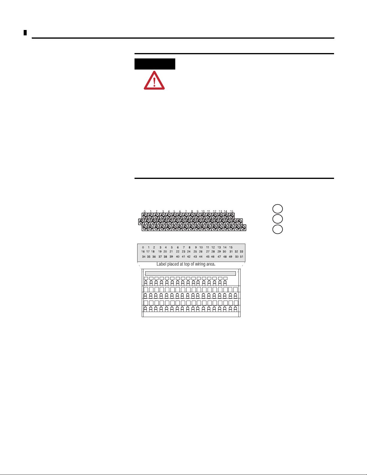
the 0–15 row (A) on the terminal base unit. (Use Belden 8761
cable for signal wiring.)
ATTENTION
Connect only one current or one voltage signal per
channel. Do not connect both current and voltage on
one channel.
2. Connect each channel signal return to:
1794-IF4I – the associated terminal on row A.
1794-OF4I – the corresponding terminal on the same row (A)
1794-IF4XOF2I – inputs – the associated terminal on row A;
outputs – the corresponding terminal on the same row (A).
3. Refer to Table 2.1 or Table 2.2. Connect +24V dc to designated
terminals on the 34-51 row (C), and 24V common todesignated
terminals on the 16–33 row (B).
ATTENTION
To reduce susceptibility to noise, power analog
modules and discrete modules from separate power
supplies. Do not exceed a length of 33 ft (10m) for
dc power cabling.
Publication 1794-6.5.8 - January 2010
Page 25
How to Install Your Analog Module 25
ATTENTION
Remove field-side power before removing or
inserting the module. This module is designed so
you can remove and insert it under backplane
power. When you remove or insert a module with
field-side power applied, an electrical arc may occur.
An electrical arc can cause personal injury or
property damage by:
• sending an erroneous signal to your system’s field
devices causing unintended machine motion
• causing an explosion in a hazardous environment
Repeated electrical arcing causes excessive wear to
contacts on both the module and its mating
connector. Worn contacts may create electrical
resistance.
±15
A
B
C
0
16±33
34±51
1794-TB3, -TB3T
Row A
Row B
Row C
Row A
Row B
Row C
1794-TB3S, -TB3TS
4. If daisy chaining the +24V dc power to the next base unit,
connect a jumper from terminal 51 on this base unit to terminal
34 on the next base unit. Connect the 24V dc common/return
from terminal 33 on this base unit to terminal 16 on the next
base unit.
Publication 1794-6.5.8 - January 2010
Page 26

26 How to Install Your Analog Module
Wiring to a 1794-TBN or 1794-TBNF Terminal Base Unit
1. Connect individual input or output wiring to the even numbered
terminals on row (B) as indicated in the table below.
2. Connect the associated return wiring to the corresponding odd
numbered terminal on row (C) for each input or output as
indicated in the table below.
3. Connect 24V dc to terminal 34 on row (C).
4. Connect 24V dc common to terminal 16 on row (B).
5. If continuing power to the next terminal base unit, connect a
jumper from terminal 51 (24V dc) on this base unit to terminal
34 on the next base unit.
16 33Even
0246810121433
16
13 57 9 11131551
34
34 51
Numbered T
Odd Numbered Terminals 1 thru 15
erminals 0 thru 14
1794-TBN, 1794-TBNF
16,
0, 2, 4, 6,
8, 10, 12, 14, 33
34, 1, 3, 5, 7,
9, 11, 13, 15, 51
B
C
If continuing common to the next terminal base unit, connect a
jumper from terminal 33 (24V dc common) on this base unit to termi
nal 16 on the next base unit.
Table 2.1
Wiring connections for 1794-TB3, -TB3T, -TB3S, -TB3TS, -TBN and -TBNF Terminal Base
Units when using the 1794-IF4I or 1794-OF4I Isolated Analog Module
Channel Signal Type Label Markings
0 Current I0 0
Current I0 Ret 1
Voltage V0 2
Voltage V0 Ret 3
1 Current I1 4
1794-TB3, -TB3T1, -TB3S, -TB3TS
1794-TBN, 1794-TBNF
Signal
Signal Return
Term in al
-
(2)
Publication 1794-6.5.8 - January 2010
Current I1 Ret 5
Voltage V1 6
Voltage V1 Ret 7
Page 27

How to Install Your Analog Module 27
Table 2.1
Wiring connections for 1794-TB3, -TB3T, -TB3S, -TB3TS, -TBN and -TBNF Terminal Base
Units when using the 1794-IF4I or 1794-OF4I Isolated Analog Module
Channel Signal Type Label Markings
1794-TB3, -TB3T1, -TB3S, -TB3TS
1794-TBN, 1794-TBNF
Signal
Signal Return
Term in al
2 Current I2 8
Current I2 Ret 9
Voltage V2 10
Voltage V2 Ret 11
3 Current I3 12
Current I3 Ret 13
Voltage V3 14
Voltage V3 Ret 15
24V dc Common
1794-TB3 – 16 through 33
(1)
1794-TB3T, -TB3TS – 17, 18, 33
1794-TBN, -TBNF – 16 and 33
+24V dc power 1794-TB3 – 34 thru 51
1794-TB3T, -TB3TS – 34, 35, 50, 51
1794-TBN, -TBNF – 34 and 51
(1)
Terminals 16 thru 33 are internally connected in the terminal base unit.
(2)
Terminal 39 through 46 are chassis ground. Terminals 36, 37, 38 and 47, 48, 49 are used or cold junction compensation.
(2)
Table 2.2
Wiring connections for the 1794-IF2XOF2I Isolated Analog Module when using 1794-TB3,
-TB3T, -TB3S, -TB3TS, -TBN and -TBNF Terminal Base Units
Channel Signal Type Label Markings
1794-TB3, -TB3T
(2)
-TB3TS
Signal
(2)
, -TB3S,
-TBN, -TBNF
Signal Return
Term in al
Input 0 Current I0 0
Current I0 Ret 1
Voltage V0 2
Voltage V0 Ret 3
Input 1 Current I1 4
Current I1 Ret 5
Voltage V1 6
Voltage V1 Ret 7
Publication 1794-6.5.8 - January 2010
Page 28
28 How to Install Your Analog Module
Table 2.2
Wiring connections for the 1794-IF2XOF2I Isolated Analog Module when using 1794-TB3,
-TB3T, -TB3S, -TB3TS, -TBN and -TBNF Terminal Base Units
Channel Signal Type Label Markings
Output 0 Current I2 8
Current I2 Ret 9
Voltage V2 10
Voltage V2 Ret 11
Output 1 Current I3 12
Current I3 Ret 13
Voltage V3 14
Voltage V3 Ret 15
24V dc Common
1794-TB3 – 16 thru 33
1794-TB3T, -TB3TS – 17, 18, 33
1794-TBN, -TBNF – 16 and 33
+24V dc power 1794-TB3 – 34 thru 51
1794-TB3T, -TB3TS – 34, 35, 50, 51
1794-TBN, -TBNF – 34 and 51
1794-TB3, -TB3T
(2)
-TB3TS
-TBN, -TBNF
Signal
Term in al
(2)
, -TB3S,
Signal Return
(1)
(1)
Terminals 16 thru 33 are internally connected in the terminal base unit.
(2)
Terminal 39 through 46 are chassis ground. Terminals 36, 37, 38 and 47, 48, 49 are used or cold junction compensation.
ATTENTION
Total current draw through the terminal base unit is
limited to 10A. Separate power connections to the
terminal base unit may be necessary.
Publication 1794-6.5.8 - January 2010
Page 29
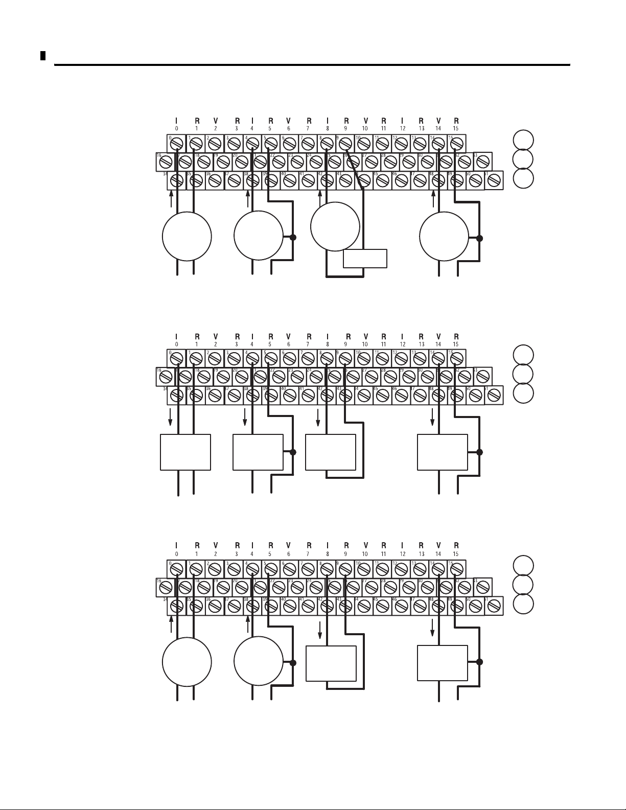
1794-IF4I
Figure 2.6
Connections ± 1794-TB3 terminal base shown
How to Install Your Analog Module 29
A
0 ±15
B
16±33
34±51
C
1794-OF4I
I I I I
+±
Current
Input
+±
ac or dc
4-Wire Current
Transmitter
+
Current
Input
+
dc only
3-Wire Current
Transmitter
Connections ± 1794-TB3 terminal base shown
I
+±
Current
Output
Device
+±
I I
+
Current
Output
Device
+
±
±±
Current
Input
+
Current only
2-Wire Current
Transmitter and External
Power Supply
I
+
Current
±±
Output
Device
±
±
24V
dc
Power Supply
+
+
Voltage
Input
+
dc only
3-Wire
Transmitter
+
Voltage
Output
Device
+
±±
A
0 ±15
B
16±33
34±51
C
±
1794-IF2XOF2I
ac or dc
4-Wire Output
Device
dc only
3-Wire Output
Device
Connections ± 1794-TB3 terminal base shown
I I
+±
Current
Input
+±
ac or dc
4-Wire Current
Transmitter
+
Current
Input
+
dc only
3-Wire Current
Transmitter
±±
Current only
2-Wire Output
Device
I
+
Current
Output
Device
±
Current only
2-Wire Output
Device
dc only
3-Wire Output
Device
I
+
Voltage
Output
Device
±
+
dc only
3-Wire Output
Device
Publication 1794-6.5.8 - January 2010
A
0 ±15
B
16±33
34±51
C
Page 30
30 How to Install Your Analog Module
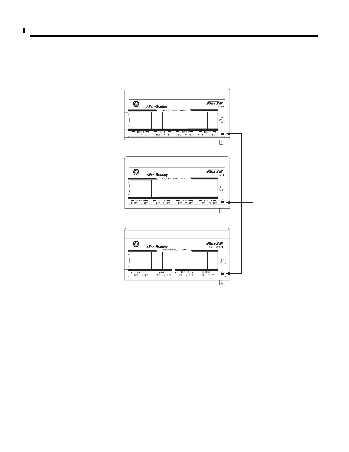
Module Indicators
The analog modules have one status indicator that is on when power
is applied to the module.
1794-IF4I
1794-OF4I
OK Status Indicator ±
Indicates power applied
to module and status.
When flashing, examine
module status word.
1794-IF2XOF2I
Chapter Summary
Publication 1794-6.5.8 - January 2010
In this chapter you learned how to install your input module in an
existing programmable controller system and how to wire to the
terminal base units.
Page 31

Module Programming
Chapter
1
Chapter Objectives
Block Transfer Programming
In this chapter, we tell you about:
• analog data format
• block transfer programming
• configuration rungs
• sample programs for the PLC-3 and PLC-5 processors
Your module communicates with the processor through bidirectional
block transfers. This is the sequential operation of both read and write
block transfer instructions.
A configuration block transfer write (BTW) is initiated when the
analog module is first powered up, and subsequently only when the
programmer wants to enable or disable features of the module. The
configuration BTW sets the bits which enable the programmable
features of the module, such as filters and signal ranges, etc. Block
transfer reads are performed to retrieve information from the module.
Block transfer read (BTR) programming moves status and data from
the module to the processor’s data table. The processor user program
initiates the request to transfer data from the module to the processor.
The transferred words contain module status, channel status and input
data from the module.
The following sample programs are minimum programs; all rungs and
conditioning must be included in your application program. You can
disable BTRs, or add interlocks to prevent writes if desired. Do not
eliminate any storage bits or interlocks included in the sample
programs. If interlocks are removed, the program may not work
properly.
Your program should monitor status bits, block transfer read and
block transfer write activity.
31 Publication 1794-6.5.8 - January 2010
Page 32
32 Module Programming
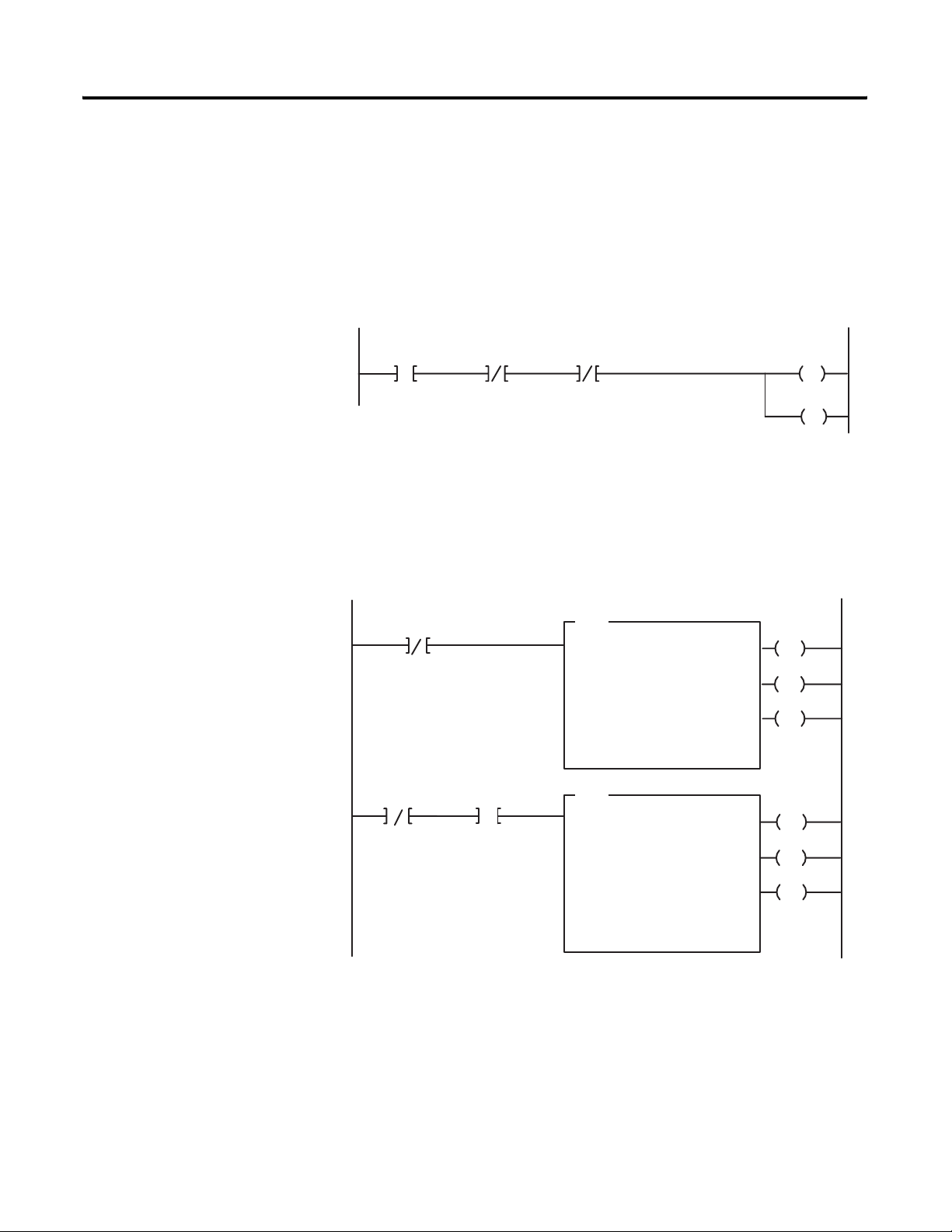
Configuration Rungs
Example Configuration Rungs
It is necessary to toggle the IC bit
isolated analog modules to accept configuration data. Once the
configuration data has been properly set up, the following rung will
reconfigure the module (this example represents sizes for the
1794-IF4I module).
Power-up Bit
B12:15
2
15
FP Bit
B12:15 B12:15 B12:54
14
If there are rungs which already perform reads and writes to the
module, no additional rungs are necessary. A simplified example of a
BTR and BTW rung for an 1794-IF4I follow (the 1794-OF4I is read
length 6, write length 7; the 1794-IF2XOF2I is read length 7, write
length 7):
(1)
(initiate configuration) for the
CF Bit
13
IC Bit
15
B12:54
L
14
1
3
BTR Enable Bit
N13:10
15
BTW Enable Bit
N3:0
15
PU Bit
N12:15
15
Optional
BTR
BLOCK
TRANSFER READ
RACK:
GROUP:
MODULE:
CONTROL:
DATA FILE:
LENGTH:
CONTINUOUS: N
BTW
BLOCK
TRANSFER WRITE
RACK:
GROUP:
MODULE:
CONTROL:
DATA FILE:
LENGTH:
CONTINUOUS: N
N13:10
N12:10
N13:0
N12:50
EN
01
0
DN
0
ER
7
EN
01
0
DN
0
ER
5
An XIC ( ––] [–– ) instruction of the Power Up bit (PU) can be inserted
to allow BTWs only when the module requires configuration (PU = 1).
Publication 1794-6.5.8 - January 2010
(1)
For systems that do not require ladder program control of configuration, set the TR bit (bit 13) to 1. Refer to
Chapter 1.
Page 33

Module Programming 33
Sample Programs for FLEX I/O Analog Modules
The following sample programs show you how to use your analog
module efficiently when operating with a programmable controller.
These programs show you how to:
• configure the module
• read data from the module
• update the module’s output channels (if used)
With RSLogix5000, just read or write the tags provided. RSLogix will
perform the transfer so an explicit block transfer is not required.
These programs illustrate the minimum programming required for
communication to take place.
PLC-3 Programming
Block transfer instructions with the PLC-3 processor use one binary
file in a data table section for module location and other related data.
This is the block transfer control file. The block transfer data file stores
data that you want transferred to your module (when programming a
block transfer write) or from your module (when programming a
block transfer read). The address of the block transfer data files are
stored in the block transfer control file.
The same block transfer control file is used for both the read
and write instructions for your module. A different block transfer
control file is required for every module.
A sample program segment with block transfer instructions is shown
Figure 1.1, and described below.
in
Publication 1794-6.5.8 - January 2010
Page 34

34 Module Programming
Figure 1.1
PLC-3 Family Sample Program Structure for a 1794-IF4I Module
Program
Action
At power-up in RUN mode, or when the
processor is switched from PROG to RUN,
the user program enables a block transfer
read.
This rung toggles the Initate Configuration
bit from 0 to 1 to 0
Then it initiates a block transfer write to
configure the module if the power--up bit
is set.
Thereafter, the program continuously
performs read block transfers.
Note: You must create the data file
for the block transfers before you
enter the block transfer instructions.
Program
Action
At power-up in RUN mode, or when the
processor is switched from PROG to RUN,
the user program enables a block transfer
read.
This rung toggles the Initate Configuration
bit from 0 to 1 to 0
Then it initiates a block transfer write to
configure the module and send data
values.
Thereafter, the program continuously
performs read block transfers and write
block transfers.
Note: You must create the data file
for the block transfers before you
enter the block transfer instructions.
BTR
BLOCK XFER READ
RACK:
GROUP:
MODULE:
CONTROL:
DATA FILE:
LENGTH:
CF Bit
B4:5
13
BTW
BLOCK XFER WRITE
RACK:
GROUP:
MODULE:
CONTROL:
DATA FILE:
LENGTH:
1
2
3
Power-up Bit
B4:5
15
Power-up Bit
B4:5
15
Block Transfer
Read Done Bit
B3:0
15
FP Bit
B4:5
14
Block Transfer
W
rite Done Bit
B3:0
05
Figure 1.2
PLC-3 Family Sample Program Structure for a 1794-OF4I Module
BTR
BLOCK XFER READ
RACK:
GROUP:
MODULE:
CONTROL:
DATA FILE:
LENGTH:
CF Bit
B7:4
13
BTW
BLOCK XFER WRITE
RACK:
GROUP:
MODULE:
CONTROL:
DATA FILE:
LENGTH:
1
2
3
Power-up Bit
B7:4
15
Block Transfer
Read Done Bit
B6:0
15
FP Bit
B7:4
14
Block Transfer
rite Done Bit
W
B6:0
05
#B3:0
#B4:0
#B3:0
#B5:0
#B6:0
#B7:0
#B6:0
#B8:0
Enable
EN
12
02
1
Done
0
DN
15
Error
ER
7
13
IC Bit
B5:4
15
B5:4
L
14
Enable
EN
02
02
1
Done
0
DN
05
Error
5
ER
03
Enable
EN
12
02
0
Done
0
DN
15
Error
ER
6
13
IC Bit
B8:6
15
B8:6
L
14
Enable
EN
02
02
0
Done
0
DN
05
Error
7
ER
03
Publication 1794-6.5.8 - January 2010
Page 35

Module Programming 35
Figure 1.3
PLC-3 Family Sample Program Structure for a 1794-IF2XOF2I Module
Program
Action
At power-up in RUN mode, or when the
processor is switched from PROG to RUN,
the user program enables a block transfer
read.
This rung toggles the Initate Configuration
bit from 0 to 1 to 0
Then it initiates a block transfer write to
configure the module and send data values
Thereafter, the program continuously
performs read block transfers and write
block transfers.
Note: You must create the data file
for the block transfers before you
enter the block transfer instructions.
1
2
3
Power-up Bit
B10:5
15
Block Transfer
Read Done Bit
B9:0
15
FP Bit
B10:5 B10:5
14
Block Transfer
W
rite Done Bit
B9:0
05
BTR
BLOCK XFER READ
RACK:
GROUP:
MODULE:
CONTROL:
DATA FILE:
LENGTH:
CF Bit
13
BTW
BLOCK XFER WRITE
RACK:
GROUP:
MODULE:
CONTROL:
DATA FILE:
LENGTH:
#B9:0
#B10:0
#B9:0
#B11:0
Enable
EN
12
02
02
Done
0
DN
15
Error
ER
7
13
IC Bit
B11:6
15
B11:6
L
14
Enable
EN
02
02
02
Done
0
DN
05
Error
7
ER
03
PLC-5 Programming
The PLC-5 program is very similar to the PLC-3 program with the
following exceptions:
• block transfer enable bits are used instead of done bits as the
conditions on each rung.
• separate block transfer control files are used for the block
transfer instructions.
Publication 1794-6.5.8 - January 2010
Page 36

36 Module Programming
Figure 1.4
PLC-5 Family Sample Program Structure for the 1794-IF4I
Program
Action
At power-up in RUN mode, or when the
processor is switched from PROG to RUN,
the user program enables a block transfer
read.
This rung toggles the Initate Configuration
bit from 0 to 1 to 0
Then it initiates a block transfer write to
configure the module if the power-up bit is
set.
Thereafter, the program continuously
performs read block transfers to configure
the module.
The pushbutton allows the user to
manually request a block transfer write.
1
2
3
BTR Enable Bit
N13:10
Power-up Bit
N12:55
15
BTR
BLOCK
TRANSFER READ
15
FP Bit
N12:55 N12:55 N12:64
14
RACK:
GROUP:
MODULE:
CONTROL:
DATA FILE:
LENGTH:
CONTINUOUS: N
CF Bit
13
Power-up
Bit
N12:55
15
BTW Enable Bit
N13:0
15
BTW
BLOCK
TRANSFER WRITE
RACK:
GROUP:
MODULE:
CONTROL:
DATA FILE:
LENGTH:
CONTINUOUS: N
02
N13:10
N12:50
THIS BIT
02
N13:0
N12:60
1
0
7
1
0
5
IC Bit
15
N12:64
L
MUST
14
EN
DN
ER
BE 1
EN
DN
ER
Publication 1794-6.5.8 - January 2010
Page 37

Figure 1.5
PLC-5 Family Sample Program Structure for the 1794-OF4I
Module Programming 37
Program
Action
At power-up in RUN mode, or when the
processor is switched from PROG to RUN,
the user program enables a block transfer
read.
This rung toggles the Initate Configuration
bit from 0 to 1 to 0
Then it initiates a block transfer write to
configure the module and send data
values.
Thereafter, the program continuously
performs read block transfers and write block
transfers.
1
2
3
BTR Enable Bit
N15:10
15
Power-up Bit
N14:14
15
BTW Enable Bit
N15:0
15
BTR
BLOCK
TRANSFER READ
RACK:
GROUP:
MODULE:
CONTROL:
DATA FILE:
LENGTH:
CONTINUOUS: N
FP Bit
N14:14 N14:14 N14:56
14
CF Bit
13
BTW
BLOCK
TRANSFER WRITE
RACK:
GROUP:
MODULE:
CONTROL:
DATA FILE:
LENGTH:
CONTINUOUS: N
N15:10
N14:10
N15:0
N14:50
2
0
0
6
THIS BIT
2
0
0
7
EN
DN
ER
IC Bit
N14:56
MUST
EN
DN
ER
15
L
14
BE 1
Publication 1794-6.5.8 - January 2010
Page 38

38 Module Programming
Figure 1.6
PLC-5 Family Sample Program Structure for the 1794-IF2XOF2I
Program
Action
At power-up in RUN mode, or when the
processor is switched from PROG to RUN,
the user program enables a block transfer
read.
This rung toggles the Initate Configuration
bit from 0 to 1 to 0
Then it initiates a block transfer write to
configure the module and send data
values.
Thereafter, the program continuously
performs read block transfers and write block
transfers.
1
2
3
BTR Enable Bit
N17:10
Power-up Bit
N16:15
15
BTW Enable Bit
N17:0
BTR
BLOCK
TRANSFER READ
15
FP Bit
14
15
RACK:
GROUP:
MODULE:
CONTROL:
DATA FILE:
LENGTH:
CONTINUOUS: N
CF Bit
13
BTW
BLOCK
TRANSFER WRITE
RACK:
GROUP:
MODULE:
CONTROL:
DATA FILE:
LENGTH:
CONTINUOUS: N
N17:10
N16:10
N17:0
N16:50
2
3
0
7
THIS BIT
2
3
0
7
EN
DN
ER
IC Bit
N16:56N16:15 N16:15
N16:56
MUST
EN
DN
ER
15
L
14
BE 1
SLC-5 Programming
More
PLC-2 Programming
The 1794 analog I/O modules are not recommended for use with
PLC-2 family programmable controllers due to the number of digits
needed for high resolution.
The SLC-5 programs (using the 1747-SN scanner) follow the same
logic as the PLC-5 family programs in the previous examples.
Differences occur in the implementation of block transfers due to the
use of “M” files in the SLC system.
Configuration data for the FLEX I/O isolated analog modules and the
1747-SN scanner must be in place before executing the following
programs. Chapter 4 contains information on the isolated analog
module configurations.
For more information on using the 1747-SN scanner module and
block transfer programming, refer to publication 1747-6.6, “Remote
I/O Scanner User Manual.”
Publication 1794-6.5.8 - January 2010
Page 39

Module Programming 39
Figure 1.7
SLC Programming for the 1794-OF4I Isolated Analog Output Module
Program
rung configures the block transfer operation
This
type, length, and RIO address at power-up. Bit
B3:100/7 must be set to 1 to indicate a BTR and
bit B3:1
BTR status is copied to the B3:0 area when a BTR
is in progress.
Unlatch the bit that continues to check the BTR status.
Action
10/7 must be 0 to indicate a BTW
0000
.
0001
0002
PowerUp Bit
S2:1
15
BTR PENDING
B3:5
0
CHECK BTR ST
B3:5
1
BTR DONE BIT
B3:0
13
ATUS
BTR_CONTROL
COP
COPY FILE
SOURCE
DEST
LENGTH
BTW_CONTROL
COP
COPY FILE
SOURCE
DEST
LENGTH
COP
COPY FILE
SOURCE
DEST
LENGTH
#B3:100
#M0:1.100
#B3:110
#M0:1.200
#M1:1.100
#B3:0
CHECK BTR ST
3
3
4
ATUS
B3:5
U
1
0003
BTW status is copied to the B3:100 area when a
BTW is in progress.
0004
Unlatch the bit that continues to check the BTW status.
T
o next page.
BTR ERROR BIT
B3:0
12
BTW PENDING
B3:15
0
CHECK BTW ST
B3:15
1
BTW DONE BIT
B3:10
13
BTW ERROR BIT
B3:10
12
ATUS
COP
COPY FILE
SOURCE
DEST
LENGTH
#M1:1.200
#B3:10
4
CHECK BTW ST
ATUS
B3:15
U
1
Publication 1794-6.5.8 - January 2010
Page 40

40 Module Programming
Program
rung buf
This
is successfully completed.
This rung buf
not successful.
Action
fers the BTR data when a transfer
fers the error code if a BTR is
0005
0006
BTR DONE BIT
B3:0
13
BTR DONE BIT
B3:0
12
COP
COPY FILE
SOURCE
DEST
LENGTH
MOV
MOVE
SOURCE
DEST
#M1:1.110
#N7:0
BTR PENDING
B3:5
U
BTR ENABLE BIT
B3:100
U
CHECK BTR ST
B3:5
L
#M1:1.103
#N7:6
0<
6
0
15
ATUS
1
6
This rung manipulates the flags for the BTW
0007
.
T
o next page.
BTW DONE BIT
B3:10
13
BTR PENDING
B3:5
U
BTR ENABLE BIT
B3:100
U
CHECK BTR ST
B3:5
L
BTW PENDING
B3:15
BTW ENABLE BIT
B3:110
CHECK BTW ST
B3:15
0
15
ATUS
1
U
0
U
15
ATUS
L
1
Publication 1794-6.5.8 - January 2010
Page 41

Module Programming 41
Program
This rung buf
not successful.
rung executes BTRs continuously
This
Action
fers the error code if a BTW is
BTW ERROR BIT
0008
0009
.
B3:10
12
BTR ENABLE BIT BTR DONE BIT
B3:100
15
B3:0
13
MOV
MOVE
SOURCE
DEST
BTR ERROR BIT
B3:0
#M1:1.203
6
#N7:17
0<
BTW PENDING
B3:15
U
BTW ENABLE BIT
CHECK BTW ST
12
0
B3:110
U
15
ATUS
B3:15
L
1
BTR PENDING
B3:5
L
0
BTR ENABLE BIT
B3:100
L
15
This rung copies the wirte data to the M0 file and
executes BTWs continuously
data for the FLEX module should be placed in
the wirte data.
. The configuration
0010
BTW ENABLE BIT
B3:110
15
T
o next page.
BTW DONE BIT
B3:10
13
BTW ERROR BIT
B3:10
12
COP
COPY FILE
SOURCE
DEST
LENGTH
BTW ENABLE BIT
#N7:10
#M1:1.210
B3:110
L
15
BTW PENDING
B3:15
L
0
Publication 1794-6.5.8 - January 2010
7
Page 42

42 Module Programming
Program
This BTR control word is moved to the M0 file
for the scanner module.
This
BTW control word is moved to the M0 file
for the scanner module.
Action
0011
0012
BTR ENABLE BIT
B3:100
15
BTR DONE BIT
B3:0
13
BTR ERROR BIT
B3:0
12
BTW ENABLE BIT
B3:110
15
BTW DONE BIT
B3:10
13
BTW ERROR BIT
B3:10
BTR CONTROL
MOV
MOVE
SOURCE
DEST
BTW CONTROL
MOV
MOVE
SOURCE
DEST
00000001000000<
B3:100
M0:1.100
B3:110
00000001000000<
M0:1.200
?<
?<
This rung toggles the initiate configuration bit
from 0 to 1 to 0.
0013
0014
POWERUP BIT
N7:4
12
FP BIT
N7:4
15
14
CF BIT
N7:4
IC BIT
N7:16
13
THIS BIT
MUST
N7:16
L
END
15
BE 1
14
Publication 1794-6.5.8 - January 2010
Page 43

Module Programming 43
Figure 1.8
SLC Programming for the 1794-IF4I Isolated Analog Input Module
Program
rung configures the block transfer operation
This
type, length, and RIO address at power-up. Bit
B3:100/7 must be set to 1 to indicate a BTR and
bit B3:1
BTR status is copied to the B3:0 area when a BTR
is in progress.
Action
10/7 must be 0 to indicate a BTW
.
0000
0001
PowerUp Bit
S2:1
15
BTR PENDING
B3:5
0
CHECK BTR ST
B3:5
1
ATUS
BTR_CONTROL
COP
COPY FILE
SOURCE
DEST
LENGTH
BTW_CONTROL
COP
COPY FILE
SOURCE
DEST
LENGTH
COP
COPY FILE
SOURCE
DEST
LENGTH
#B3:100
#M0:1.100
3
#B3:110
#M0:1.200
3
#M1:1.100
#B3:0
4
0002
Unlatch the bit that continues to check the BTR status.
0003
BTW status is copied to the B3:100 area when a
BTW is in progress.
BTR DONE BIT
B3:0
1
BTR ERROR BIT
B3:0
12
BTW PENDING
B3:15
0
CHECK BTW ST
B3:15
1
o next page.
T
ATUS
COP
COPY FILE
SOURCE
DEST
LENGTH
CHECK BTR ST
#M1:1.200
#B3:10
ATUS
B3:5
U
1
4
Publication 1794-6.5.8 - January 2010
Page 44

44 Module Programming
Program
Unlatch
This rung buf
is successfully completed.
Action
the bit that continues to check the BTW status.
fers the BTR data when a transfer
0004
0005
BTW DONE BIT
B3:10
13
BTW ERROR BIT
B3:10
12
BTR DONE BIT
B3:0
13
COP
COPY FILE
SOURCE
DEST
LENGTH
CHECK BTW ST
#M1:1.110
#N7:0
BTR PENDING
B3:5
U
BTR ENABLE BIT
B3:100
U
15
CHECK BTR ST
B3:5
L
ATUS
B3:15
U
1
7
0
ATUS
1
This rung buf
not successful.
fers the error code if a BTR is
0006
BTR ERROR BIT
T
o next page.
B3:0
MOV
MOVE
12
SOURCE
DEST
M1:1.103
N7:7
BTR PENDING
B3:5
U
BTR ENABLE BIT
B3:100
U
CHECK BTR ST
B3:5
L
0<
0
15
ATUS
1
Publication 1794-6.5.8 - January 2010
Page 45

Module Programming 45
Program
This rung manipulates the flags for the BTW
This rung buf
not successful.
Action
fers the error code if a BTW is
BTW DONE BIT
0007
.
0008
B3:10
13
BTW ERROR BIT
B3:10
12
MOV
MOVE
SOURCE
DEST
BTW ENABLE BIT
CHECK BTW ST
BTW PENDING
BTW ENABLE BIT
CHECK BTW ST
M1:1.203
6
N7:15
0<
BTW PENDING
B3:15
U
0
B3:110
U
15
B3:15
L
1
B3:15
B3:110
B3:15
ATUS
U
0
U
15
ATUS
U
1
This
rung executes BTRs continuously
BTR ENABLE BIT BTR DONE BIT
0009
.
B3:100
T
o next page.
15
B3:0
13
BTR ERROR BIT
B3:0
12
BTR PENDING
B3:5
L
0
BTR ENABLE BIT
B3:100
L
15
Publication 1794-6.5.8 - January 2010
Page 46

46 Module Programming
Program
This rung executes a BTW to configure the
module when the power-up bit (PU) is set.
This BTR control word is moved to the M0 file
for the scanner module.
Action
0010
0011
PU BIT
N7:5
BTR ENABLE BIT
BTR ERROR BIT
BTW ENABLE
15
B3:100
15
BTR DONE BIT
B3:0
13
B3:0
BIT
B3:110
15
BTW DONE
B3:10
13
BTW ERROR
BITBIT
B3:10
12
BTR CONTROL
MOV
MOVE
SOURCE
DEST
COP
COPY FILE
SOURCE
DEST
LENGTH
00000001000000<
BTW ENABLE BIT
BTW PENDING
B3:100
M0:1.100
?<
#N7:10
#M0:1.210
5
B3:110
L
15
B3:15
L
0
This
BTW control word is moved to the M0 file
for the scanner module.
This rung toggles the initiate configuration bit
from 0 to 1 to 0.
0012
0013
BTW ENABLE BIT
B3:110
15
BTW DONE BIT
B3:10
BTW ERROR BIT
B3:10
POWERUP BIT
N7:5
15
12
BTR CONTROL
MOV
MOVE
SOURCE
DEST
13
12
FP BIT
N7:5
14
CF BIT
N7:5
13
00000001000000<
B3:110
M0:1.200
THIS BIT
?<
IC BIT
N7:14
15
MUST
BE 1
N7:14
L
14
Publication 1794-6.5.8 - January 2010
0014
END
Page 47

Program
rung configures the block transfer operation
This
type, length, and RIO address at power-up. Bit
B3:100/7 must be set to 1 to indicate a BTR and
bit B3:1
Action
10/7 must be 0 to indicate a BTW
.
Module Programming 47
Figure 1.9
SLC Programming for the 1794-IF2XOF2I Isolated Analog Input/Output Module
PowerUp Bit
S2:1
0000
15
BTR_CONTROL
COP
COPY FILE
SOURCE
DEST
LENGTH
BTW_CONTROL
COP
COPY FILE
SOURCE
DEST
LENGTH
#B3:100
#M0:1.100
3
#B3:110
#M0:1.200
3
0001
BTR status is copied to the B3:0 area when a BTR
is in progress.
0002
Unlatch the bit that continues to check the BTR status.
0003
BTW status is copied to the B3:100 area when a
BTW is in progress.
BTR PENDING
B3:5
0
CHK BTR ST
BTR DONE BIT
BTR ERROR BIT
BTW PENDING
CHK BTW STATUS
ATUS
B3:5
1
B3:0
13
B3:0
12
B3:5
0
B3:5
COP
COPY FILE
SOURCE
DEST
LENGTH
COP
COPY FILE
SOURCE
DEST
LENGTH
#M1:1.100
#B3:0
#M1:1.100
#B3:0
4
CHK BTR ST
B3:5
4
ATUS
U
1
0004
1
BTW PENDING
B3:15
0
CHK BTW STATUS
B3:15
1
T
o next page.
COP
COPY FILE
SOURCE
DEST
LENGTH
#M1:1.200
#B3:10
4
Publication 1794-6.5.8 - January 2010
Page 48

48 Module Programming
Program
Unlatch
This rung buf
is successfully completed.
Action
the bit that continues to check the BTW status.
fers the BTR data when a transfer
0005
0006
BTW DONE BIT
B3:10
13
BTW ERROR BIT
B3:10
12
BTR DONE BIT
B3:0
13
COP
COPY FILE
SOURCE
DEST
LENGTH
CHK BTW STATUS
#M1:1.110
#N7:0
7
BTR PENDING
B3:5
U
B3:100
U
B3:5
L
0
15
ATUS
1
BTR ENABLE BIT
CHK BTR ST
B3:15
U
1
This rung buf
not successful.
fers the error code if a BTR is
0007
BTR DONE BIT
T
o next page.
B3:0
MOV
MOVE
12
SOURCE
DEST
M1:1.103
N7:7
BTR PENDING
B3:5
U
BTR ENABLE BIT
B3:100
U
CHECK BTR ST
B3:5
L
6
0<
0
15
ATUS
1
Publication 1794-6.5.8 - January 2010
Page 49

Module Programming 49
Program
This rung manipulates the flags for the BTW
This rung buf
not successful.
Action
fers the error code if a BTW is
BTW DONE BIT
0008
.
0009
B3:10
13
BTW ERROR BIT
B3:10
12
MOV
MOVE
SOURCE
DEST
BTW ENABLE BIT
CHK BTW STATUS
BTW PENDING
BTW ENABLE BIT
CHECK BTW ST
M1:1.203
N7:17
0<
BTW PENDING
B3:15
U
0
B3:110
U
15
B3:15
L
1
B3:15
U
B3:110
U
B3:15
L
0
15
ATUS
1
rung executes BTRs continuously
This
BTR ENABLE BIT BTR DONE BIT
0010
.
B3:100
T
o next page.
15
B3:0
13
BTR ERROR BIT
B3:0
12
BTR PENDING
B3:5
L
0
BTR ENABLE BIT
B3:100
L
15
Publication 1794-6.5.8 - January 2010
Page 50

50 Module Programming
Program
This rung executes a BTW to configure the module
when the power-up bit is set. The configuration
data for the FLEX module should be placed in the
wirte data.
This BTR control word is moved to the M0 file
for the scanner module.
This
for the scanner module.
Action
BTW control word is moved to the M0 file
0011
0012
0013
BTR ENABLE BIT
B3:100
15
BTR DONE BIT
B3:0
13
BTR ERROR BIT
B3:0
12
BTW ENABLE BIT
B3:110
15
BTW DONE BIT
B3:10
BTW ENABLE
BIT
B3:110
15
BTW DONE BIT
B3:10
13
BTW ERROR BIT
B3:10
BTR CONTROL
MOV
MOVE
SOURCE
DEST
BTR CONTROL
MOV
MOVE
SOURCE
DEST
12
00000001000000<
00000000000000<
COP
COPY FILE
SOURCE
DEST
LENGTH
BTW ENABLE BIT
BTW PENDING
B3:100
M0:1.100
?<
B3:110
M0:1.200
?<
#N7:10
#M0:1.210
B3:110
L
15
B3:15
L
0
7
This rung toggles the initiate configuration bit
from 0 to 1 to 0.
Publication 1794-6.5.8 - January 2010
0014
0015
0016
BTW ERROR BIT
B3:10
POWERUP BIT
N7:5
13
12
FP BIT
N7:5
15
14
Thereafter
, the program continuously performs read block transfers.
CF BIT
N7:5
13
MOV
MOVE
SOURCE
DEST
THIS BIT
N7:0
<
N7:11
<
IC BIT
N7:16
MUST
N7:16
L
END
15
BE 1
14
Page 51

Module Programming 51
Chapter Summary
In this chapter, you learned how to program your programmable
controller. You were given sample programs for your PLC-3 and PLC-5
family processors.
Publication 1794-6.5.8 - January 2010
Page 52

52 Module Programming
Publication 1794-6.5.8 - January 2010
Page 53

Chapter
4
Writing Configuration to and Reading Status from Your Module with a Remote I/O Adapter
Chapter Objectives
Configuring Your Analog Module
In this chapter, we tell you about:
• configuring your module’s features
• entering your data
• reading data from your module
• read block format
Because of the many analog devices available and the wide variety of
possible configurations, you must configure your module to conform
to the analog device and specific application that you have chosen.
The module is configured using a group of data table words that are
transferred to the module using a block transfer write instruction.
The software configurable features available are:
• input/output range selection
• data type (two’s complement, two’s complement percent, binary
and offset binary)
PLC-5 family programmable controllers that use 6200 software
programming tools can take advantage of the IOCONFIG utility to
configure these modules. IOCONFIG uses menu-based screens for
configuration without having to set individual bits in particular
locations. Refer to your 6200 software literature for details.
TIP
53 Publication 1794-6.5.8 - January 2010
RSLogix family programmable controllers that use
RSLogix software programming tools can take
advantage of the configuration GUI to configure
these modules.
Page 54

54 Writing Configuration to and Reading Status from Your Module with a Remote I/O Adapter
Range Selection
Individual input channels are configurable to operate with the
following voltage or current ranges:
Table 4.1
Range Selection
Input channel Configuration
Input Values Data Format % Underrange/
% Overrange
Channel not configured
4–20mA signed 2’s complement 4% Under; 4% Over
±10V signed 2’s complement 2% Under, 2% Over
±5V signed 2’s complement 4% Under, 4% Over
0–20mA signed 2’s complement % 0% Under, 4% Over
4-20mA signed 2’s complement % 4% Under, 4% Over
0–10V signed 2’s complement % 0% Under, 2% Over
±10V signed 2’s complement % 2% Under, 2% Over
0–20mA binary 0% Under, 4% Over
0–10V binary 0% Under, 2% Over
0–5V binary 0% Under, 4% Over
Safe State Selection
±20mA offset binary, 8000H = 0mA 4% Under, 4% Over
4–20mA offset binary, 8000H = 4mA 4% Under, 4% Over
±10V offset binary, 8000H = 0V 2% Under, 2% Over
±5V offset binary, 8000H = 0V 4% Under, 4% Over
You can select individual channel ranges using the designated words
of the write block transfer instruction. Refer to the Bit/Word
description for your particular module for word and bit numbers.
You can select the analog values that your output module will
maintain in the event of a network communication error. When the
enable bit is cleared by a communication error, the analog outputs
will automatically switch to the values set in the safe state analog
words as defined by the safe state source bits. This allows you to
select a reset to 0V/0mA, or hold the outputs at their last state when
using the remote I/O adapter on remote I/O. Additionally, safe state
values can be setup using ControlNet, DeviceNet or other network
adapter.
Data Format
Publication 1794-6.5.8 - January 2010
The input/output data exchanged between the module and the
adapter is available in two’s complement, two’s complement percent,
binary and offset binary (refer to the range selection table above).
Page 55

Writing Configuration to and Reading Status from Your Module with a Remote I/O Adapter 55
Real Time Sampling
Real time sampling (RTS) provides data gathered at precise intervals
for use by the processor. You set a word in the block transfer write
data file to enable RTS.
The real time sample programmed interval is the time at which
updated information will be supplied to the processor. When set to
“0” the module will default to each channel’s fastest update rate,
which is dependent on the nominal range of the input and the filter
setting set to “no low pass.”
When the IT interrupt toggle bit is set (1), interleaving of module
interrupts occurs, ensuring exchange of critical data when channels
are configured for their fastest update times. RTSI and “no low pass
filter” must be 0 in order for the module to recognize this feature. This
groups data update rates for all channels to the slowest configuration
setting of any of the channels. In addition, channel update rates for all
channels with a 7.5ms update rate are reduced to 5.0ms. When reset
(0), real time sampling and filter features are enabled.
Table 4.2
Real Time Sample Interval
Configuration Nominal Range Channel
Update Rate
(RTS = 0)
1 4-20mA 7.5ms 5.0ms
2 ±10V 2.5ms 2.5ms
3 ±5V 2.5ms 2.5ms
4 0-20mA 7.5ms 5.0ms
5 4-20mA 7.5ms 5.0ms
6 0-10V 5.0ms 5.0ms
7 ±10V 5.0ms 5.0ms
8 0-20mA 2.5ms 2.5ms
9 4-20mA 7.5ms 5.0ms
A 0-–10V 2.5ms 2.5ms
B 0-5V 2.5ms 2.5ms
C ±20mA 2.5ms 2.5ms
D 4-20mA 7.5ms 5.0ms
E ±10V 2.5ms 2.5ms
F ±5V 2.5ms 2.5ms
(1)
Channel filter set to “no low pass.”
(1)
Channel Update Rate (RTS
and Filter = 0)
(1)
and IT = 1
Publication 1794-6.5.8 - January 2010
Page 56

56 Writing Configuration to and Reading Status from Your Module with a Remote I/O Adapter
The real time sample interval can be set from 0 to 30s, in increments
of 5ms. Set the real time sample interval in binary using 15 bits in the
block transfer write word.
Word/Dec. Bit 15 14 13 12 11 10 09 08 07 06 05 04 03 02 01 00
Word/Octal Bit 17 16 15 14 13 12 11 10 07 06 05 04 03 02 01 00
Word 3 0 Real Time Sample Programmed Interval
The individual channel update times determines how fast you can get
new information collectively from the module. The module gathers
the data from each input and makes it available to the processor. For
example, if channel 0 is 2.5ms, channel 1 is 5.0ms, and channel 2 is
7.5ms, and RTS = 0, each channel will be updated at its stated rate. If
RTS is set to 5ms, only channels 0 and 1 are fast enough to be
included in the real time sample. In order to include channel 2 in your
synchronous sample, you must set the RTS to 10ms minimum. Your
updated information will be accurate for all inputs/outputs as viewed
at the last update before the time of your request.
Slowest
Channel Update T
Internal R
TS Timer = 10ms
ime= 7.5ms
ATTENTION
0
0
Do not set your real time sample interval less than
the slowest channel’s update time.
TS updated
4 inputs and R
10 20 30 40
5101520 307.5 27.5 37.53525 40
TS updated
4 inputs and R
17.5
TS updated
4 inputs and R
TS updated
4 inputs and R
Input Filtering
Publication 1794-6.5.8 - January 2010
The input modules have selectable input filtering built into the A/D
converter. The filter attenuates the input signal beginning at the speci
fied frequency. You can select from 150, 300, 600, and 1200Hz with
low pass filters of none, 100ms, 500ms or 1000ms. Each channel filter
-
Page 57

Writing Configuration to and Reading Status from Your Module with a Remote I/O Adapter 57
can be set individually. Select the filter based on your system requirements.
A/D Conversion Rate Low Pass Filter
1200Hz No low pass
1200Hz 100ms low pass
1200Hz 500ms low pass
1200Hz 1000ms low pass
600Hz No low pass
600Hz 100ms low pass
600Hz 500ms low pass
600Hz 1000ms low pass
300Hz No low pass
300Hz 100ms low pass
300Hz 500ms low pass
300Hz 1000ms low pass
Reading Data From Your Module
Mapping Data for the Analog Modules
150Hz No low pass
150Hz 100ms low pass
150Hz 500ms low pass
150Hz 1000ms low pass
Read programming moves status and data from the module to the
processor’s data table. The processor’s user program initiates the
request to transfer data from the input module (or combination
module) to the processor.
The following read and write words and bit/word descriptions
describe the information written to and read from the analog modules.
Each word is composed of 16 bits.
Publication 1794-6.5.8 - January 2010
Page 58

58 Writing Configuration to and Reading Status from Your Module with a Remote I/O Adapter
8 Input Analog Module (Cat. No. 1794-IF4I)
Module
Image
Table 4.3
Analog Input Module (1794-IF4I) Read
Word/Dec. Bit 15 14 13 12 11 10 09 08 07 06 05 04 03 02 01 00
Word/Octal Bit 17 16 15 14 13 12 11 10 07 06 05 04 03 02 01 00
I/O Image
Input Size
1 to 7 Words
Output Size
0 to 5 Words
Input Data Channel 0
Input Data Channel 1
Input Data Channel 2
Input Data Channel 3
Real Time Sample
PU FP CF BD DN
UnderrangeOverrange
Set to 0EN
Channel
Filters
Channel Configuration
Real Time Sample Programmed Interval
IC
1
IT
TR
RV QK CK GO
Channel #
Read Word 0 Analog Value Channel 0
Word 1 Analog Value Channel 1
Word 2 Analog Value Channel 2
Word 3 Analog Value Channel 3
Word 4 Real Time Sample
Word 5 PU FP CF 0 Reserved 0 0 0 0 0 BD DN 0
Word 6 0 0 0 0 0 0 0 0 V3 V2 V1 V0 U3 U2 U1 U0
Where:
PU = Power up unconfigured state
FP = Field power off
CF = In configuration mode
BD = Calibration bad
DN = Calibration accepted
U = Under range for specified channel
V = Overrange for specified channel
Publication 1794-6.5.8 - January 2010
Page 59

Writing Configuration to and Reading Status from Your Module with a Remote I/O Adapter 59
Table 4.4
Word/Bit Descriptions for the 1794-IF4I Analog Input Module
Read Word Decimal Bit
Definition
(Octal Bit)
Word 0 Bits 00-15
(00-17)
Word 1 Bits 00-15
(00-17)
Word 2 Bits 00-15
(00-17)
Word 3 Bits 00-15
(00-17)
Word 4 Bits 00-15
(00-17)
Channel 0 analog data – Real time input data per your
configuration
Channel 1 analog data – Real time input data per your
configuration
Channel 2 analog data – Real time input data per your
configuration
Channel 3 analog data – Real time input data per your
configuration
Real Time Sample. The elapsed time in increments
programmed by the real time sample interval.
Word 5 Bits 00 Reserved
Bits 01 Calibration Done bit (DN). – This bit is set to 1 after a
calibration cycle is
Bits 02 Calibration Bad bit (BD). – This bit is set to 1 if the channel
calibration
Bits 03–07 Set to 0.
Bits 08–11
Reserved
(10-12)
Bit 12 (14) Set to 0
Bit 13 (15) Configuration mode bit (CF) – This bit is set (1) when the
calibration mode is selected (bit 15, word 5 in the block
transfer write set to 1). When this bit is set (1), the module
status indicator flashes.
Bit 14 (16) Field Power Off bit (FP) – This bit is set (1) when the 24V
field power fails. When this bit is set (1), the module status
indicator flashes.
Bit 15 (17) Power Up (unconfigured state) bit (PU). – This bit is set (1)
when the configuration word is all zeroes (0) due to a reset
(adapter power cycle or module insertion) or a cleared
configuration word (all 0). When this bit is set (1), the module
status indicator flashes.
Word 6 Bits 00-03 Underrange bits (U). – These bits are set (1) when the input
channel is below a preset limit as defined by the configuration
selected. U0 (bit 00) corresponds to input channel 0 and U1 (bit
01) corresponds to input channel 1, etc. Refer to Table 4.B.
Bits 04-07 Overrange bits (V). – These bits are set (1) when the input
channel is above a preset limit as defined by the configuration
selected. Bit 04 corresponds to input channel 0 and bit 05
Bits 08–15
corresponds to input channel 1, etc. Refer to
Not used. Set to 0.
Table 4.8.
(10-17)
Publication 1794-6.5.8 - January 2010
Page 60

60 Writing Configuration to and Reading Status from Your Module with a Remote I/O Adapter
Table 4.5
Analog Input Module (1794-IF4I) Write Configuration Block
Word/Dec. Bit 15 14 13 12 11 10 09 08 07 06 05 04 03 02 01 00
Word/Octal Bit 17 16 15 14 13 12 11 10 07 06 05 04 03 02 01 00
Word 0 EN 0 0 0 0 0 0 0 0 0 0 0 0 0 0 0
Word 1 Chnl 3 Filter Chnl 2 Filter Chnl 1 Filter Chnl 0 Filter
Word 2 Chnl 3 Configuration Chnl 2 Configuration Chnl 1 Configuration Chnl 0 Configuration
Word 3 0 Real Time Sample Programmed Interval
Word 4 IC 1 TR IT 0 0 0 0 RV QK CK GO Channel Number
Where:
EN = Not used on the 1794-IF4I.
IC = Initiate configuration bit
TR = Transparent bit
IT = Interrupt Toggle bit
RV = Revert to defaults bit
QK = Quick calibration
CK = Calibration clock
GO = Gain offset select
Table 4.6
Word/Bit Descriptions for the 1794-IF4I Analog Input ModuleWrite
Write Word Decimal Bit (Octal
Definition
Bit)
Word 0 Bits 00–14 (00–16) Not used. Set to 0.
Bit 15 (17) Output enable bit (EN). – Not used in the 1794-IF4I module.
Word 1 Channels 0 through 3 Filter Selections (refer to Table 4.7 )
Bits 00–03 Channel 0 Filter Setting
Bits 04–07 Channel 1 Filter Setting
Bits 08–11 (10–13) Channel 2 Filter Setting
Bits 12–15 (14–17) Channel 3 Filter Setting
Word 2 Channel Configuration (refer to Table 4.B )
Bits 00–03 Channel 0 Configuration
Bits 04–07 Channel 1 Configuration
Bits 08–11 (10–13) Channel 2 Configuration
Bits 12–15 (14–17) Channel 3 Configuration
Word 3 Bits 00–14 (00–16) Real Time Sample Interval – Programs the interval of the real time sample. Can be varied
from 0 to 30 seconds (30000 decimal). Resolution is in ms with granularity in 5ms steps.
Bit 15 (17) Not used. Set to 0.
Publication 1794-6.5.8 - January 2010
Page 61

Writing Configuration to and Reading Status from Your Module with a Remote I/O Adapter 61
Table 4.6
Word/Bit Descriptions for the 1794-IF4I Analog Input ModuleWrite
Write Word Decimal Bit (Octal
Definition
Bit)
Word 4 Bit 00–03 Channel calibration selection bit. When this bit is set (1), the channel can be calibrated
using the calibration clock bit (CK). Bit 00 corresponds to input channel 0, bit 01 corresponds to
input channel 1, it 02 corresponds to input channel 2, bit 03 corresponds to input channel 3
Bit 04 Gain/Offset selection bit (GO). – When this bit is cleared, a 0 to 1 to 0 transition of the CK
bit performs on offset calibration. When this bit is 1, the module is directed to do a gain
calibration.
Bit 05 Calibration clock bit (CK). – When this bit is set to 1 (calibration mode), the calibration
coeffiicient for the selected channels is accepted. When this bit is reset (0), the accepted
calibration coefficients for the selected channels are stored, applied, and the calibration mode
exited. Monitor status bits DN and BD for succesful calibration.
Bit 06 Quick Calibration bit (QK). – Normally reset (0). When this bit is set (1) during a calibration
sequence, the calibration coefficient is stored to all related configurations for the selected
channels. NOTE: This method of calibration quickly calibrates the selected channels, however
you will not be within the rated accuracy of the module.
Bit 07 Revert to defaults bit (RV). – Normally reset (0). When set (1) during a calibration procedure,
default values for selected channels are used for the calibration coefficient.NOTE: You will not
be within the rated accuracy of the module.
Bits 08-11 (10-13) Not used. Set to 0.
For IF4ICFXT only:
Bit 8 — FastStepResponse (FR) forces the A/D to skip the FIR stage if an input step occurs.
An averaging algorithm is temporarily used instead of the FIR filter in the A/D to provide a
quicker response.
Bit 9 — FIRFilterDisable (SK) bypasses the FIR filter stage in the A/D.
Bit 10 — ChopModeDisable (CH) disables the chop mode in the A/D. Chop mode is used to
reduce offsets between input and output of the analog section of the A/D.
(1)
Note: Module level settings that only affect 150 Hz, 300 Hz, and 600 Hz conversion rate
settings.
Bit 12 (14) Interrupt Toggle bit (IT) – This bit, when set (1), permits interleaving of module interrupts
ensuring exchange of critical data when channels are configured for their fastest update times.
RTSI and “no low pass filter” must be 0 in order for the module to recognize this feature. This
groups data update rates for all channels to the slowest configuration setting of any of the
channels. In addition, channel update rates for all channels with a 7.5ms update rate are
reduced to 5.0ms. When reset (0), real time sampling and filter features are enabled.
Bit 13 (15) Transparent bit (TR). – This bit, when set to 1, permits configuration to be changed without
using the IC bit. Default setting for this bit is True (1)
Bit 14 (16) Always set to 1.
Bit 15 (17) Initiate Configuration bit (IC). – When set (1), instructs the module to enter configuration
mode. Present configuration data prior to or coincident with IC being set. Once IC returns to 0,
the configuration is applied and any subquent configuration information is ignored until IC is
toggled.
(1)
For changes in tag values like the CH bit in the IF4ICFXT to take effect, the tag either must be included in a ladder rung or or a configuration download forced using the
configuration tab in the RSLogix GUI.
Publication 1794-6.5.8 - January 2010
Page 62

62 Writing Configuration to and Reading Status from Your Module with a Remote I/O Adapter
Table 4.7
Setting the Input Filter
Bits Channel
03 02 01 00 Input 0
07 06 05 04 Input 1
11 10 09 08 Input 2
15 14 13 12 Input 3
A/D Conversion
Rate
0 0 0 0 1200Hz No low pass
0 0 0 1 1200Hz 100ms low pass
0 0 1 0 1200Hz 500ms low pass
0 0 1 1 1200Hz 1000ms low pass
0 1 0 0 600Hz No low pass
0 1 0 1 600Hz 100ms low pass
Low Pass Filter
Table 4.8
Configuring Your Input Module
Input Channel Configuration
03 02 01 00 Set these bits for Channel 0
07 06 05 04 Set these bits for Channel 1
11 10 09 08 Set these bits for Channel 2
15 14 13 12 Set these bits for Channel 3
0 1 1 0 600Hz 500ms low pass
0 1 1 1 600Hz 1000ms low pass
1 0 0 0 300Hz No low pass
1 0 0 1 300Hz 100ms low pass
1 0 1 0 300Hz 500ms low pass
1 0 1 1 300Hz 1000ms low pass
1 1 0 0 150Hz No low pass
1 1 0 1 150Hz 100ms low pass
1 1 1 0 150Hz 500ms low pass
1 1 1 1 150Hz 1000ms low pass
Publication 1794-6.5.8 - January 2010
Page 63

Table 4.8
Configuring Your Input Module
Writing Configuration to and Reading Status from Your Module with a Remote I/O Adapter 63
Bit Settings Input
Values
Data Format % Underrange
%Overrange
0 0 0 0 Channel not configured
0 0 0 1 4–20mA signed 2’s complement 4% Under; 4%
Over
0 0 1 0 ±10V signed 2’s complement 2% Under, 2%
Over
0 0 1 1 ±5V signed 2’s complement 4% Under, 4%
Over
0 1 0 0 0–20mA signed 2’s complement %0% Under, 4%
Over
0 1 0 1 4-20mA signed 2’s complement %4% Under, 4%
Over
0 1 1 0 0–10V signed 2’s complement %0% Under, 2%
Over
0 1 1 1 ±10V signed 2’s complement %2% Under, 2%
Over
1 0 0 0 0–20mA binary 0% Under, 4%
Over
Input Range
(2)
Module Update
Rate
Hexadecimal Decimal (RTSI = 0)(RTSI =
0)
IT = 1
<0000–7878> <0000–30840> 7.5ms 5.0ms
<831F–7CE1> <–31969–
2.5ms 2.5ms
31969>
<8618–79E8> <–31208–
2.5ms 2.5ms
31208>
0–2710> 0–10000> 7.5ms 5.0ms
<0–2710> <0–10000> 7.5ms 5.0ms
0–2710> 0–10000> 5.0ms 5.0ms
<–D8F0–2710> <–10000–
5.0ms 5.0ms
10000>
0000–F3CF> 0000–62415> 2.5ms 2.5ms
1 0 0 1 4–
20mA
binary 4% Under, 4%
(1)
Over
1 0 1 0 0–10V binary 0% Under, 2%
Over
1 0 1 1 0–5V binary 0% Under, 4%
Over
1 1 0 0 ±20mA offset binary, 8000H =
0mA
1 1 0 1 4–20mA offset binary, 8000H =
4mA
4% Under, 4%
Over
4% Under, 4%
Over
1 1 1 0 ±10V offset binary, 8000H = 0V2% Under, 2%
Over
1 1 1 1 ±5V offset binary, 8000H = 0V4% Under, 4%
Over
(1)
Underrange for 4-20mA occurs in the blind area below 0 (3.2mA).
(2)
< and > indicate the overrun beyond actual range (about 5%).
0000–F0F1> 0000–61681> 7.5ms 5.0ms
0000–F9C2> 0000–63938> 2.5ms 2.5ms
0000–F3CF> 0000–62415> 2.5ms 2.5ms
<0618–F9E8> <1560–63976> 2.5ms 2.5ms
<8000–F878> <32768–63608> 7.5ms 5.0ms
<031F–FCE1> <799–64737> 2.5ms 2.5ms
<0618–F9E8> <1560–63976> 2.5ms 2.5ms
Publication 1794-6.5.8 - January 2010
Page 64

64 Writing Configuration to and Reading Status from Your Module with a Remote I/O Adapter
4 Isolated Output Analog Module (Cat. No. 1794-OF4I)
Module
Image
Table 4.9
Analog Output Module (1794-OF4I) Read
I/O Image
Input Size
0 to 6 Words
Output Size
2 to 7 Word
Read Back Channel 0
Read Back Channel 1
Read Back Channel 2
Read Back Channel 3
PU FP CF BD DN
Hold
Outputs
S1 S0
IC RV QK CK GO
1 Q3 Q2 Q1 Q0TR IT
Set to 0EN
Output Data Channel 0
Output Data Channel 1
Output Data Channel 2
Output Data Channel 3
Channel Configuration
Wire-off
Channel #
Word/Dec. Bit 15 14 13 12 11 10 09 08 07 06 05 04 03 02 01 00
Word/Octal Bit 17 16 15 14 13 12 11 10 07 06 05 04 03 02 01 00
Read Word 0 Read Back Channel 0
Word 1 Read Back Channel 1
Word 2 Read Back Channel 2
Word 3 Read Back Channel 3
Word 4 PU FP CF 0 Reserved 0 0 0 0 0 BD DN 0
Word 5 0 0 0 0 P3 P2 P1 P0 0 0 0 0 W3 W2 W1 W0
Where:
PU = Power up unconfigured state
FP = Field power off
CF = In configuration mode
BD = Calibration bad
DN = Calibration accepted
P0 thru P3 = Output holding in response to Q0 thru Q3
W0 thru W3 = Wire off current loop status for channels 0 thru 3 respectively. (Not used on voltage outputs.)
Publication 1794-6.5.8 - January 2010
Page 65

Writing Configuration to and Reading Status from Your Module with a Remote I/O Adapter 65
Table 4.10
Bit/Word Descriptions for the 1794-OF4I Analog Output Module Read
Read Word Decimal Bit
Definition
(Octal Bit)
Word 0 Bits 00-15 (00-17) Read Back Channel 0 – During normal operation, it is a copy of the output of channel
0. During an EN transition, it is the condition of the output as determined by S1 and S0.
Read back is an image of what the user has sent as output to the module; no checks are
performed on the data.
Word 1 Bits 00-15 (00-17) Read Back Channel 1 – During normal operation, it is a copy of the output of channel
1. During an EN transition, it is the condition of the output as determined by S1 and S0.
Read back is an image of what the user has sent as output to the module; no checks are
performed on the data.
Word 2 Bits 00-15 (00-17) Read Back Channel 2 – During normal operation, it is a copy of the output of channel
2. During an EN transition, it is the condition of the output as determined by S1 and S0.
Read back is an image of what the user has sent as output to the module; no checks are
performed on the data.
Word 3 Bits 00-15 (00-17) Read Back Channel 3 – During normal operation, it is a copy of the output of channel
3. During an EN transition, it is the condition of the output as determined by S1 and S0.
Read back is an image of what the user has sent as output to the module; no checks are
performed on the data.
Word 4 Bits 00 Reserved
Bits 01 Calibration Done bit (DN). – This bit is set to 1 after a calibration cycle is completed.
Bit 02 Calibration Bad bit (BD). – This bit is set to 1 if the channel calibration coefficients
cannot be saved or read properly.
Bits 03–07 Set to 0.
Bits 08–11
Reserved
(10-12)
Bit 12 (14) Set to 0
Bit 13 (15) Configuration mode bit (CF) – This bit is set (1) when the configuration mode is
selected (bit 15, word 5 in the block transfer write set to 1). When this bit is set, the
module status indicator flashes.
Bit 14 (16) Field Power Off bit (FP) – This bit is set (1) when the 24V field power fails. When this
bit is set (1), the module status indicator flashes.
Bit 15 (17) Power Up (unconfigured state) bit (PU). – This bit is set (1) when the configuration
word is all zeroes (0) due to a reset (adapter power cycle or module insertion) or a cleared
configuration word (all 0). When this bit is set, the module status indicator flashes.
Word 5 Bits 00–03 Wire-Off status bits. (W). – These bits, when set (1), indicate the corresponding
current output channel is open. W0 corresponds to channel 0, W1 corresponds to
channel 2, etc.
Bits 04–07 Set to 0.
Bits 10–11
(12-13)
Hold output bits (P). – These bits are set (1) in response to Q0 or Q1 and a transition of
the EN bit. When P0 or P1 is set (1), they indicate that the output is holding at the level in
the readback data for the respective channel. These bits return to 0 when the output data
matches the readback output data.
Bits 12–15
Set to 0.
(14-17)
Publication 1794-6.5.8 - January 2010
Page 66

66 Writing Configuration to and Reading Status from Your Module with a Remote I/O Adapter
Table 4.11
Analog Output Module (1794-OF4I) Write Configuration Block
Word/Dec. Bit 15 14 13 12 11 10 09 08 07 06 05 04 03 02 01 00
Word/Octal Bit 17 16 15 14 13 12 11 10 07 06 05 04 03 02 01 00
Write Word 0 EN S1 S0 0 0 0 0 0 0 0 0 0 0 0 0 0
Word 1 Output Data – Channel 0
Word 2 Output Data – Channel 1
Word 3 Output Data – Channel 2
Word 4 Output Data – Channel 3
Word 5 Output Chnl 3
Configuration
Output Chnl 2
Configuration
Output Chnl 1
Configuration
Word 6 IC 1 TR IT Q3 Q2 Q1 Q0 RV QK CK GO Channel Number
Where:
EN = Enable outputs; 0 = output follows S1/S0, 1 = output enabled
IC = Initiate configuration bit
TR = Transparent bit
IT = Interrupt Toggle bit
Q0–3 = Request for outputs to hold
RV = Revert to defaults bit
QK = Quick calibration
CK = Calibration clock
GO = Gain offset select
Output Chnl 0
Configuration
Table 4.12
Range Selection Bits and Real Time Output Update Rate for the 1794-OF4I Isolated Output Module
Configuration Bits Nominal
MSD LSD Hexadecimal Decimal
Range
Data Type Output Values Update
0 0 0 1 4-20mA 2’s complement <0000–7878> <0000–30840> 5.0ms
0 0 1 0 ±10V 2’s complement <8618–79E8> <–31208–31208> 2.5ms
0 0 1 1 ±5V 2’s complement <8618–79E8> <–31208–31208> 2.5ms
0 1 0 0 0-20mA 2’s complement % 0–10000> 0–10000> 5.0ms
0 1 0 1 4-20mA 2’s complement % <0–10000> <0–10000> 5.0ms
0 1 1 0 0-10V 2’s complement % 0–10000> 0–10000> 5.0ms
0 1 1 1 ±10V 2’s complement <–10000–10000> <–10000–10000> 5.0ms
1 0 0 0 0-20mA binary 0000–F3CF> 0000–62415> 2.5ms
1 0 0 1 4-20mA binary 0000–F0F1> 0000–61681> 5.0ms
1 0 1 0 0-–10V binary 0000–F3CF> 0000–62415> 2.5ms
1 0 1 1 0-5V binary 0000–F3CF> 0000–62415> 2.5ms
1 1 0 0 ±20mA offset binary <8000–F9E8> 32768–63976> 2.5ms
1 1 0 1 4-20mA offset binary <8000–F878> <32768–63608> 5.0ms
Rate
Publication 1794-6.5.8 - January 2010
Page 67

Writing Configuration to and Reading Status from Your Module with a Remote I/O Adapter 67
Table 4.12
Range Selection Bits and Real Time Output Update Rate for the 1794-OF4I Isolated Output Module
1 1 1 0 ±10V offset binary <0618–F9E8> <1560–63976> 2.5ms
1 1 1 1 ±5V offset binary <0618–F9E8> <1560–63976> 2.5ms
Table 4.13
Word/Bit Descriptions for the 1794-OF4I Analog Output Module
Write Word Decimal Bit
Definition
(Octal Bit)
Word 0 Bits 00–14
Not used
(00–16)
Bits 13–14
(15-16)
Safe State Source bits (S1/S0). – When EN is 0, these bits designate the source of
the safe state data.
Bit 13 = 0, bit 14 = 1 – reset outputs to 0V/0mA (used with 1794-ASB/C)
Bit 13 = 1, bit 14 = 1 – hold output at its current level (used with 1794-ASB/C)
Bit 13 = 0; bit 14 = 0 – Safe state data is in output data words
Bit 15 (17) Output enable bit (EN). – When set (1), the outputs are enabled. This bit must be set
in order for the real time data to appear at the outputs. If this bit is not set (0), the
outputs will be determined by S1/S0.
Word 1 Bits 00–15
(00–17)
Word 2 Bits 00–15
(00-17)
Word 3 Bits 00–15
(00-17)
Word 4 Bits 00–15
(00-17)
Channel 0 output data. – The output data is real time data formatted to the selected
configuration. (This data is also safe state data when directed by S1 and S0.)
Channel 1 output data. – The output data is real time data formatted to the selected
configuration. (This data is also safe state data when directed by S1 and S0.)
Channel 2 output data. – The output data is real time data formatted to the selected
configuration. (This data is also safe state data when directed by S1 and S0.)
Channel 3 output data. – The output data is real time data formatted to the selected
configuration. (This data is also safe state data when directed by S1 and S0.)
Word 5 Channel Configuration (refer to page 4-66)
Bits 00–03 Channel 0 Configuration
Bits 04–07 Channel 1 Configuration
Bits 08–11
Channel 2 Configuration
(10-13)
Bits 12–15
Channel 3 Configuration
(14-17)
Publication 1794-6.5.8 - January 2010
Page 68

68 Writing Configuration to and Reading Status from Your Module with a Remote I/O Adapter
Table 4.13
Word/Bit Descriptions for the 1794-OF4I Analog Output Module
Write Word Decimal Bit
Definition
(Octal Bit)
Word 6 Bit 00–03 Channel calibration selection bit. When this bit is set (1), the channel can be
calibrated using the calibration clock bit (CK). Bit 00 corresponds to output channel 0, bit
01 corresponds to output channel 1, it 02 corresponds to output channel 3, bit 03
corresponds to output channel 4
Bit 04 Gain/Offset selection bit (GO). – When this bit is cleared, a 0 to 1 to 0 transition of
the CK bit performs on offset calibration. When this bit is 1, the module is directed to do
a gain calibration.
Bit 05 Calibration clock bit (CK). – When this bit is set to 1 (calibration mode), the
calibration coeffiicient for the selected channels is accepted. When this bit is reset (0),
the accepted calibration coefficients for the selected channels are stored, applied, and
the calibration mode exited. Monitor status bits DN and BD for succesful calibration.
Bit 06 Quick Calibration bit (QK). – Normally reset (0). When this bit is set (1) during a
calibration sequence, the calibration coefficient is stored to all related configurations
for the selected channels. NOTE: Although this method of calibration quickly calibrates
the selected channels, they will not be within the rated accuracy of the module.
Bit 07 Revert to defaults bit (RV). – Normally reset (0). When set (1) during a calibration
procedure, default values for selected channels are used for the calibration coefficient.
NOTE: They will not be within the rated accuracy of the module.
Bits 08–11
(10–13)
Request for hold outputs (Q). – Channel request bits that instruct an output to hold its
output level when EN transitions from 1 to 0 to 1. When EN is 0, outputs go to a safe
state dictated by S1/S0. When EN returns to 1, the outputs will hold their level until the
output data equals the output level. P0–P3 indicates channels holding. Output read back
data shows what level is being held. Q0 = bit 08 (10) = channel 0; Q1 = bit 09 (11) =
channel 1, etc.
Bit 12 (14) Interrupt Toggle bit (IT) – This bit, when set (1), permits interleaving of module
interrupts ensuring exchange of critical data when channels are configured for their
fastest update times. RTSI and “no low pass filter” must be 0 in order for the module to
recognize this feature. This groups data update rates for all channels to the slowest
configuration setting of any of the channels. In addition, channel update rates for all
channels with a 7.5ms update rate are reduced to 5.0ms. When reset (0), real time
sampling and filter features are enabled.
Bit 13 (15) Transparent bit (TR). – This bit, when set to 1, permits configuration to be changed
Bit 14 (16) Set to 1
Bit 15 (17) Initiate Configuration bit (IC). – When set (1), instructs the module to enter
Publication 1794-6.5.8 - January 2010
without using the IC bit.
configuration mode. Present configuration data prior to or coincident with IC being set.
Once IC returns to 0, the configuration is applied and any subquent configuration
information is ignored until IC is toggled.
Page 69

Read
Writing Configuration to and Reading Status from Your Module with a Remote I/O Adapter 69
2 Input/2 Output Analog Combo Module (Cat. No. 1794-IF2XOF2I)
Module
Image
I/O Image
Input Size
0 to 7 Words
PU FP CF BD DN
Input Data Channel 0
Input Data Channel 1
Read Back Output Data Channel 0
Read Back Output Data Channel 1
Real Time Sample
V1 V0 U1 U0W1 W0P1 P0
Write
Table 4.14
Analog Combo Module (1794-IF2XOF2I) Read
Word/Dec. Bit 15 14 13 12 11 10 09 08 07 06 05 04 03 02 01 00
Word/Octal Bit 17 16 15 14 13 12 11 10 07 06 05 04 03 02 01 00
Read Word 0 Input Data Channel 0
Word 1 Input Data Channel 1
Word 2 Read Back Output Channel 0
Word 3 Read Back Output Channel 1
Word 4 0 Real Time Sample
Output Size
0 to 7 Words
Set to 0EN S1 S0
Output Data Channel 0
Output Data Channel 1
Channel Filters
Channel
Configuration
Real Time Sample Programmed Interval
IC RV QK CK GO
1
Q0Q1TR IT
Channel #
Publication 1794-6.5.8 - January 2010
Page 70

70 Writing Configuration to and Reading Status from Your Module with a Remote I/O Adapter
Table 4.14
Analog Combo Module (1794-IF2XOF2I) Read
Word 5 PU FP CF 0 Reserved 0 0 0 0 0 BD DN 0
Word 6 0 0 0 0 P1 P0 0 0 0 0 V1 V0 W1 W0 U1 U0
Where:
PU = Power up unconfigured state
FP = Field power off
CF = In configuration mode
BD = Calibration bad
DN = Calibration accepted
P0 and P1 = Output holding in response to Q0 thru Q1
W0 and W1 = Wire off current loop status for input channels 0 and 1 respectively. (Not used on voltage outputs.)
U0 and U1 = Underrange for input channels o and 1 respectively.
V0 and V1 = Overrange for input channels o and 1 respectively.
Table 4.15
Configuring Your Input Channels
Input Channel Configuration
03 02 01 00 Set these bits for Channel 0
07 06 05 04 Set these bits for Channel 1
Bit Settings Input
Values
Data Format % Underrange
%Overrange
Input Range
Hexadecimal Decimal (RTSI = 0)(RTSI =
0 0 0 0 Channel not configured
(2)
Module Update
Rate
0)
IT = 1
0 0 0 1 4–20mA signed 2’s complement 4% Under; 4%
Over
0 0 1 0 ±10V signed 2’s complement 2% Under, 2%
Over
0 0 1 1 ±5V signed 2’s complement 4% Under, 4%
Over
0 1 0 0 0–20mA signed 2’s complement %0% Under, 4%
Over
0 1 0 1 4-20mA signed 2’s complement %4% Under, 4%
Over
0 1 1 0 0–10V signed 2’s complement %0% Under, 2%
Over
0 1 1 1 ±10V signed 2’s complement %2% Under, 2%
Over
1 0 0 0 0–20mA binary 0% Under, 4%
Over
1 0 0 1 4–
20mA
Publication 1794-6.5.8 - January 2010
binary 4% Under, 4%
(1)
Over
<0000–7878> <0000–30840> 7.5ms 5.0ms
<831F–7CE1> <–31969–
2.5ms 2.5ms
31969>
<8618–79E8> <–31208–
2.5ms 2.5ms
31208>
0–2710> 0–10000> 7.5ms 5.0ms
<0–2710> <0–10000> 7.5ms 5.0ms
0–2710> 0–10000> 5.0ms 5.0ms
<–D8F0–2710> <–10000–
5.0ms 5.0ms
10000>
0000–F3CF> 0000–62415> 2.5ms 2.5ms
0000–F0F1> 0000–61681> 7.5ms 5.0ms
Page 71

Table 4.15
Configuring Your Input Channels
Writing Configuration to and Reading Status from Your Module with a Remote I/O Adapter 71
1 0 1 0 0–10V binary 0% Under, 2%
Over
1 0 1 1 0–5V binary 0% Under, 4%
Over
1 1 0 0 ±20mA offset binary, 8000H =
0mA
1 1 0 1 4–20mA offset binary, 8000H =
4mA
4% Under, 4%
Over
4% Under, 4%
Over
1 1 1 0 ±10V offset binary, 8000H = 0V2% Under, 2%
Over
1 1 1 1 ±5V offset binary, 8000H = 0V4% Under, 4%
Over
(1)
Underrange for 4-20mA occurs in the blind area below 0 (3.2mA).
(2)
< and > indicate the overrun beyond actual range (about 5%).
Table 4.16
Setting the Input Filter
Bits Channel
03 02 01 00 Input Channel 0
0000–F9C2> 0000–63938> 2.5ms 2.5ms
0000–F3CF> 0000–62415> 2.5ms 2.5ms
<0618–F9E8> <1560–63976> 2.5ms 2.5ms
<8000–F878> <32768–63608> 7.5ms 5.0ms
<031F–FCE1> <799–64737> 2.5ms 2.5ms
<0618–F9E8> <1560–63976> 2.5ms 2.5ms
07 06 05 04 Input Channel 1
A/D Conversion
Low Pass Filter
Rate
0 0 0 0 1200Hz No low pass
0 0 0 1 1200Hz 100ms low pass
0 0 1 0 1200Hz 500ms low pass
0 0 1 1 1200Hz 1000ms low pass
0 1 0 0 600Hz No low pass
0 1 0 1 600Hz 100ms low pass
0 1 1 0 600Hz 500ms low pass
0 1 1 1 600Hz 1000ms low pass
1 0 0 0 300Hz No low pass
1 0 0 1 300Hz 100ms low pass
1 0 1 0 300Hz 500ms low pass
1 0 1 1 300Hz 1000ms low pass
1 1 0 0 150Hz No low pass
1 1 0 1 150Hz 100ms low pass
1 1 1 0 150Hz 500ms low pass
1 1 1 1 150Hz 1000ms low pass
Publication 1794-6.5.8 - January 2010
Page 72

72 Writing Configuration to and Reading Status from Your Module with a Remote I/O Adapter
Table 4.17
Word/Bit Descriptions for the 1794-IF2XOF2I Isolated Analog Combo Module Read
Write Word Decimal Bit
Definition
(Octal Bit)
Word 0 Bits 00–15
Input Channel 0 input data – Real time input data per your configuration
(00–17)
Word 1 Bits 00–15
Input Channel 1 input data – Real time input data per your configuration
(00–17)
Word 2 Bits 00–15
(00–17)
Read Back Output Channel 0 – During normal operation, it is a copy of the output of
channel 0. During an EN transition, it is the condition of the output as determined by S1
and S0. Note: Read back data is an image of what the user has sent as output to the
module; no checks are performed on the data.
Word 3 Bits 00–15
(00–17)
Read Back Output Channel 1 – During normal operation, it is a copy of the output of
channel 1. During an EN transition, it is the condition of the output as determined by S1
and S0. Note: Read back data is an image of what the user has sent as output to the
module; no checks are performed on the data.
Word 4 Bits 00–15
(00–17)
Real Time Sample. The elapsed time in increments programmed by the real time
sample interval.
Word 5 Bits 00 Reserved
Bits 01 Calibration Done bit (DN). – This bit is set to 1 after a calibration cycle is completed.
Bits 02 Calibration Bad bit (BD). – This bit is set to 1 if the channel calibration coefficients
cannot be saved or read properly.
Bits 03-07 Set to 0.
Bits 08-11
Reserved
(10-12)
Bit 12 (14) Set to 0
Bit 13 (15) Configuration mode bit (CF) – This bit is set (1) when the configuration mode is
selected (bit 15, word 6 in the block transfer write set to 1). When this bit is set (1), the
module status indicator flashes.
Bit 14 (16) Field Power Off bit (FP) – This bit is set (1) when the 24V field power fails. When this
bit is set (1), the module status indicator flashes.
Bit 15 (17) Power Up (unconfigured state) bit (PU). – This bit is set (1) when the configuration
word is all zeroes (0) due to a reset (adapter power cycle or module insertion) or a
cleared configuration word (all 0). When this bit is set (1), the module status indicator
flashes.
Publication 1794-6.5.8 - January 2010
Page 73

Writing Configuration to and Reading Status from Your Module with a Remote I/O Adapter 73
Table 4.17
Word/Bit Descriptions for the 1794-IF2XOF2I Isolated Analog Combo Module Read
Write Word Decimal Bit
(Octal Bit)
Word 6 Bits 00-01 Underrange bits (U). – These bits are set (1) when the input channel is below a preset
Bits 02-03 Wire-Off status bits. (W). – These bits, when set (1), indicate the corresponding
Bits 04-05 Overrange bits (V). – These bits are set (1) when the input channel is above a preset
Bits 06-09
(06-11)
Bits 10-11
(12-13)
Bits 12-15
(14-17)
Table 4.18
Analog Combo Module (1794-IF2XOF2I) Read
Definition
limit as defined by the configuration selected. U0 (bit 00) corresponds to input channel 0
and U1 (bit 01) corresponds to input channel 1, etc. Refer to
Table 4.15.
current output channel is open. W0 (bit 02) corresponds to channel 0, and W1 (bit 03)
corresponds to channel 1.
limit as defined by the configuration selected. Bit 04 corresponds to input channel 0 and
bit 05 corresponds to input channel 1. Refer to
Table 4.15.
Not used. Set to 0.
Hold output bits (P). – These bits are set (1) in response to Q0 or Q1 and transition of
the EN bit. When P0 or P1 is set (1), they indicate that the output is holding at the level
in the readback data for the respective channel. These bits return to 0 when the output
data matches the readback output data.
Not used. Set to 0.
Word/Dec. Bit 15 14 13 12 11 10 09 08 07 06 05 04 03 02 01 00
Word/Octal Bit 17 16 15 14 13 12 11 10 07 06 05 04 03 02 01 00
Write Word 0 EN S1 S0 0 0 0 0 0 0 0 0 0 0 0 0 0
Word 1 Output Data Channel 0
Word 2 Output Data Channel 1
Word 3 0 0 0 0 0 0 0 0 Input Channel 1 Filter Input Channel 0 Filter
Word 4 Output Channel 1
Configuration
Output Channel 0
Configuration
Input Channel 1
Configuration
Input Channel 0
Configuration
Word 5 0 Real Time Sample Programed Interval
Word 6 IC 1 TR IT Q1 Q2 0 0 RV QK CK GO Input Channel 0
Configuration
Where:
EN = Enable outputs; 0 = output follows S1/S0, 1 = output enabled
IC = Initiate configuration bit
IT = Interrupt Toggle bit
TR = Transparent bit
Q0 and Q1 = Request for outputs to hold
RV = Revert to defaults bit
QK = Quick calibration
CK = Calibration clock
GO = Gain offset select
Publication 1794-6.5.8 - January 2010
Page 74

74 Writing Configuration to and Reading Status from Your Module with a Remote I/O Adapter
Table 4.19
Configuring Your Outputs for the 1794-IF2XOF2I Analog Combo Module
Configuration
Bits
Nominal
Range
Data Type
Output Values
(1)
Update
Rate
MSD LSD Hexadecimal Decimal
0 0 0 1 4-20mA 2’s complement <0000–7878> <0000–30840> 5.0ms
0 0 1 0 ±10V 2’s complement <8618–79E8> <–31208–31208> 2.5ms
0 0 1 1 ±5V 2’s complement <8618–79E8> <–31208–31208> 2.5ms
0 1 0 0 0-20mA 2’s complement % 0–2710> 0–10000> 5.0ms
0 1 0 1 4-20mA 2’s complement % <0–2710> <0–10000> 5.0ms
0 1 1 0 0-10V 2’s complement % 0–2710> 0–10000> 5.0ms
0 1 1 1 ±10V 2’s complement % <–D8F0–2710> <–10000–10000> 5.0ms
1 0 0 0 0-20mA binary 0000–F3CF> 0000–62415> 2.5ms
1 0 0 1 4-20mA binary 0000–F0F1> 0000–61681> 5.0ms
1 0 1 0 0–10V binary 0000–F3CF> 0000–62415> 2.5ms
1 0 1 1 0-5V binary 0000–F3CF> 0000–62415> 2.5ms
1 1 0 0 ±20mA offset binary 8000–F9E8> 32768–63976> 2.5ms
1 1 0 1 4-20mA offset binary <8000–F878> <32768–63608> 5.0ms
1 1 1 0 ±10V offset binary <0618–F9E8> <1560–63976> 2.5ms
1 1 1 1 ±5V offset binary <0618–F9E8> <1560–63976> 2.5ms
(1)
< and > indicate the overrun beyond actual range (about 5%).
Table 4.20
Word/Bit Descriptions for the 1794-IF2XOF2I Analog Combo Module Write
Write Word Decimal Bit
(Octal Bit)
Word 0 Bits 00–14
(00–16)
Bit 13–14 (15–16) Safe State Source bits (S1/S0). – When EN is 0, these bits designate the source of
Bit 15 (17) Output enable bit (EN). – When set (1), the outputs are enabled. This bit must be set
Word 1 Bits 00–15
(00–17)
Publication 1794-6.5.8 - January 2010
Definition
Not used
the safe state data.
Bit 13 = 0, bit 14 = 1 – reset outputs to 0V/0mA (used with 1794-ASB/C)
Bit 13 = 1, bit 14 = 1 – hold output at its current level (used with 1794-ASB/C)
Bit 13 = 0; bit 14 = 0 – Safe state data is in output data words
in order for the real time data to appear at the outputs. If this bit is not set (0), the
outputs will be determined by S1/S0.
Output Channel 0 data. Refer to Table 4.19.
Page 75

Writing Configuration to and Reading Status from Your Module with a Remote I/O Adapter 75
Table 4.20
Word/Bit Descriptions for the 1794-IF2XOF2I Analog Combo
Module Write
Write Word Decimal Bit
Definition
(Octal Bit)
Word 2 Bits 00–15
Output Channel 1 data. Refer to Table 4.19.
(00–17)
Word 3 Input Channels 0 and 1 Filter Selections (refer to Table 4.16)
Bits 00–01 Channel 0 Filter Setting
Bits 04–07 Channel 1 Filter Setting
Word 4 Channel configuration
Bits 00–03 Input Channel 0 Configuration – Refer to Table 4.15.
Bits 04–07 Input Channel 1 Configuration – Refer to Table 4.15.
Bits 08–11
Output Channel 0 Configuration – Refer to Table 4.19.
(10–13)
Bits 12–15
Output Channel 1 Configuration – Refer to Table 4.19.
(14–17)
Word 5 Bits 00–14
(00–16)
Real Time Sample Interval – Programs the interval of the real time sample. Can be
varied from 0 to 30 seconds (30000 decimal). Resolution is in ms with granularity in 5ms
steps. (see
page 4-55)
Publication 1794-6.5.8 - January 2010
Page 76

76 Writing Configuration to and Reading Status from Your Module with a Remote I/O Adapter
Table 4.20
Word/Bit Descriptions for the 1794-IF2XOF2I Analog Combo
Module Write
Write Word Decimal Bit
(Octal Bit)
Word 6 Bit 00–03 Channel calibration selection bit. When this bit is set (1), the channel can be
Bit 04 Gain/Offset selection bit (GO). – When this bit is cleared, a 0 to 1 to 0 transition of
Bit 05 Calibration clock bit (CK). – When this bit is set to 1 (calibration mode), the
Bit 06 Quick Calibration bit (QK). – Normally reset (0). When this bit is set (1) during a
Bit 07 Revert to defaults bit (RV). – Normally reset (0). When set (1) during a calibration
Bits 08–09
(10–11)
Bits 10–11
(12–13)
Bit 12 (14) Interrupt Toggle bit (IT) – This bit, when set (1), permits interleaving of module
Definition
calibrated using the calibration clock bit (CK). Bit 00 corresponds to input channel 0, bit
01 corresponds to input channel 1, it 02 corresponds to output channel 0, bit 03
corresponds to output channel 1.
the CK bit performs on offset calibration. When this bit is 1, the module is directed to do
a gain calibration.
calibration coeffiicient for the selected channels is accepted. When this bit is reset (0),
the accepted calibration coefficients for the selected channels are stored, applied, and
the calibration mode exited. Monitor status bits DN and BD for succesful calibration.
calibration sequence, the calibration coefficient is stored to all related configurations
for the selected channels. NOTE: This method of calibration quickly calibrates the
selected channels, however you will not be within the rated accuracy of the module.
procedure, default values for selected channels are used for the calibration coefficient.
NOTE: You will not be within the rated accuracy of the module.
Not used. Set to 0.
Request for hold outputs (Q). – Channel request bits that instruct an output to hold its
output level when EN transitions from 1 to 0 to 1. When EN is 0, outputs go to a safe
state dictated by S1/S0. When EN returns to 1, the outputs will hold their level until the
output data equals the output level. P0–P3 indicates channels holding. Output read back
data shows what level is being held. Q0 = bit 08 (10) = channel 0; Q1 = bit 08 (10) =
channel 1, etc.
interrupts ensuring exchange of critical data when channels are configured for their
fastest update times. RTSI and “no low pass filter” must be 0 in order for the module to
recognize this feature. This groups data update rates for all channels to the slowest
configuration setting of any of the channels. In addition, channel update rates for all
channels with a 7.5ms update rate are reduced to 5.0ms. When reset (0), real time
sampling and filter features are enabled.
Bit 13 (15) Transparent bit (TR). – This bit, when set to 1, permits configuration to be changed
Bit 15 (17) Initiate Configuration bit (IC). – When set (1), instructs the module to enter
Chapter Summary
Publication 1794-6.5.8 - January 2010
without using the IC bit.
configuration mode. Present configuration data prior to or coincident with IC being set.
Once IC returns to 0, the configuration is applied and any subquent configuration
information is ignored until IC is toggled.
In this chapter, you read how to configure your module’s features and
enter your data.
Page 77

Chapter
5
Communication and I/O Image Table Mapping with the DeviceNet/ControlNet Adapter
Chapter Objectives
About RSNetWorx and RSLogix
Polled I/O Structure
In this chapter, you will read about:
• RSNetWorx and RSLogix software
• I/O structure
• image table mapping
• factory defaults
RSNetWorx is a software tool used in conjunction with RSLogix to
configure your FLEX I/O DeviceNet or ControlNetadapter and its
related modules. This software tool can be connected to the adapter
via the DeviceNet network. The Ethernet IP adapter only requires
RSLogix to configure the modules.
Output data is received by the adapter in the order of the installed I/O
modules. The Output data for Slot 0 is received first, followed by the
Output data for Slot 1, and so on up to slot 7.
The first word of input data sent by the adapter is the Adapter Status
Word. This is followed by the input data from each slot, in the order
of installed I/O modules. The Input data from Slot 0 is first after the
status word, followed by Input data from Slot 2, and so on to slot 7.
DeviceNet Adapter
Read Data
Adapter
Status
Slot 0 Input Data
Network
READ
Network WRITE
77 Publication 1794-6.5.8 - January 2010
Slot 1 Input Data
...
Slot 7 Input Data
Write Data
Slot 0 Output Data
Slot 1 Output Data
...
Slot 7 Output Data
...
...
Read
Write
I/O Module
Slot 0
I/O Module
Slot 1
...
I/O Module
Slot 7
Page 78

78 Communication and I/O Image Table Mapping with the DeviceNet/ControlNet Adapter
Adapter Input Status Word
The input status word consists of:
• I/O module fault bits – 1 status bit for each slot
• node address changed – 1 bit
• I/O status – 1 bit
15Bit: 01234567810 through 15
9
I/O Module Fault Bits
Not Used
I/O State Bit
Node Address Changed Bit
Slot 7
Slot 6
Slot 5
Slot 4
Slot 3
Slot 2
Slot 1
Slot 0
The adapter input status word bit descriptions are shown in the following table.
Bit Description Bit Explanation
I/O Module Faults 0 This bit is set (1) when an error is detected in slot position 0.
1 This bit is set (1) when an error is detected in slot position 1.
2 This bit is set (1) when an error is detected in slot position 2.
3 This bit is set (1) when an error is detected in slot position 3.
4 This bit is set (1) when an error is detected in slot position 4.
5 This bit is set (1) when an error is detected in slot position 5.
6 This bit is set (1) when an error is detected in slot position 6.
7 This bit is set (1) when an error is detected in slot position 7.
Node Address Changed 8 This bit is set (1) when the node address switch setting has been
changed sing power up.
I/O State 9 Bit = 0 – idle
Bit = 1 – run
10 thru 15 Not used – sent as zeroes.
Publication 1794-6.5.8 - January 2010
Possible causes for an I/O Module Fault are:
• transmission errors on the FLEX I/O backplane
• a failed module
• a module removed from its terminal base
• incorrect module inserted in a slot position
• the slot is empty
The node address changed bit is set when the node address switch
setting has been changed since power up. The new node address
does not take affect until the adapter has been powered down and
then powered back up.
Page 79

Communication and I/O Image Table Mapping with the DeviceNet/ControlNet Adapter 79
Mapping Data into the Image Table
Module Description Catalog
4 Input Isolated Analog Module 1794-IF4I page 5-79
4 Output Isolated Analog Module 1794-OF4I page 5-86
2 in/2 out Isolated Analog Combo Module 1794-IF2XOF2I page 5-91
FLEX I/O analog modules are supported by the DeviceNet adapter.
For image table mapping refer to:
Number:
4 Input Isolated Analog Module (Cat. No. 1794-IF4I) Image Table
Mapping
Module
Image
I/O Image
Input Size
1 to 7Words
Output Size
0 to 8 Word
PU FP CF BD DN
IC
1
TR IT
Input Data Channel 0
Input Data Channel 1
Input Data Channel 2
Input Data Channel 3
Real Time Sample
Set to 0EN
Channel Filters
Channel Configuration
Real Time Sample Programmed Interval
RV QK CK GO
Not used
Not used
Not used
UnderrangeOverrange
Channel #
Table 5.1
Analog Input Module (1794-IF4I, 1794-IF4ICFXT) Read
Word/Dec. Bit 15 14 13 12 11 10 09 08 07 06 05 04 03 02 01 00
Word/Octal Bit 17 16 15 14 13 12 11 10 07 06 05 04 03 02 01 00
Read Word 1 Analog Value Channel 0
Word 2 Analog Value Channel 1
Word 3 Analog Value Channel 2
Word 4 Analog Value Channel 3
Word 5 Real Time Sample
Word 6 PU FP CF 0 Reserved 0 0 0 0 0 BD DN 0
Word 7 0 0 0 0 0 0 0 0 V3 V2 V1 V0 U3 U2 U1 U0
Where:
PU = Power up unconfigured state
FP = Field power off
CF = In configuration mode
BD = Calibration bad
DN = Calibration accepted
U = Under range for specified channel
V = Overrange for specified channel
Publication 1794-6.5.8 - January 2010
Page 80

80 Communication and I/O Image Table Mapping with the DeviceNet/ControlNet Adapter
Table 5.2
Analog Input Module (1794-IF4ICFXT) Write
Dec. 15 14 13 12 11 10 9 8 7 6 5 4 3 2 1 0
Oct. 17 16 15 14 13 12 11 10 7 6 5 4 3 2 1 0
Word 0 EN 0 0 0 0 0 0 0 0 0 0 0 0 0 0 0
Word 1 Channel 3 Filter Channel 2 Filter Channel 1 Filter Channel 0 Filter
Word 2 Ch 3 Configuration Ch 2 Configuration Ch 1 Configuration Ch 0 Configuration
Word 3 0 Real Time Sample Interval
Word 4 IC 1 TR IT 0 CH SK FS RV QK CK GO Channel Number
Word 5 Reserved
Where :
EN = Enable bit (not used on input module)
IC = Initiate Configuration bit
TR = Transparent bit
IT = Interrupt toggle bit
CH - Chop Mode Disable — use to disable the chop mode. Chop mode used by the module to reduce offset and drift errors. The
default is chop mode enabled (0).
SK = FIR Filter Disable — use to disable the FIR filter. The Finite Impulse Response filter is used by the module to improve signal
stability. The default is FIR filter enabled (0).
FS = Fast Step Response — use to enable a fast step response algorithm. The fast step response algorithm, upon sensing a step
input, uses an averaging method rather than the FIR filter. The FIR goes back into operation once the input has settled. The
default is fast step response disabled (0).
RV = Revert to default bit
QK = Quick calibration
CK = Calibration clock
GO = Gain Offset select
Table 5.3
Analog Input Module (1794-IF4I) Write Configuration Block
Word/Dec. Bit 15 14 13 12 11 10 09 08 07 06 05 04 03 02 01 00
Word/Octal Bit 17 16 15 14 13 12 11 10 07 06 05 04 03 02 01 00
Word 1 EN 0 0 0 0 0 0 0 0 0 0 0 0 0 0 0
Word 2 Chnl 3 Filter Chnl 2 Filter Chnl 1 Filter Chnl 0 Filter
Word 3 Chnl 3 Configuration Chnl 2 Configuration Chnl 1 Configuration Chnl 0 Configuration
Word 4 0 Real Time Sample Programmed Interval
Word 5 IC 1 TR IT 0 0 0 0 RV QK CK GO Channel Number
Word 6 Not used
Word 7 Not used
Word 7 Not used
Where:
EN = Not used on the 1794-IF4I.
IC = Initiate configuration bit
TR = Transparent bit
IT = Interrupt Toggle bit
RV = Revert to defaults bit
QK = Quick calibration
CK = Calibration clock
GO = Gain offset select
Publication 1794-6.5.8 - January 2010
Page 81

Communication and I/O Image Table Mapping with the DeviceNet/ControlNet Adapter 81
Table 5.4
Setting the Input Filter
Bits Channel
03 02 01 00 Input 0
07 06 05 04 Input 1
11 10 09 08 Input 2
15 14 13 12 Input 3
A/D Conversion
Low Pass Filter
Rate
0 0 0 0 1200Hz No low pass
0 0 0 1 1200Hz 100ms low pass
0 0 1 0 1200Hz 500ms low pass
0 0 1 1 1200Hz 1000ms low pass
0 1 0 0 600Hz No low pass
0 1 0 1 600Hz 100ms low pass
Input Channel Configuration
03 02 01 00 Set these bits for Channel 0
07 06 05 04 Set these bits for Channel 1
11 10 09 08 Set these bits for Channel 2
15 14 13 12 Set these bits for Channel 3
Bit Settings Input
Values
0 0 0 0 Channel not configured
Data Format % Underrange
0 1 1 0 600Hz 500ms low pass
0 1 1 1 600Hz 1000ms low pass
1 0 0 0 300Hz No low pass
1 0 0 1 300Hz 100ms low pass
1 0 1 0 300Hz 500ms low pass
1 0 1 1 300Hz 1000ms low pass
1 1 0 0 150Hz No low pass
1 1 0 1 150Hz 100ms low pass
1 1 1 0 150Hz 500ms low pass
1 1 1 1 150Hz 1000ms low pass
Table 5.5
Configuring Your Input Module
%Overrange
Input Range
Hexadecimal Decimal (RTSI = 0) (RTSI = 0)
(2)
Module Update Rate
IT = 1
Publication 1794-6.5.8 - January 2010
Page 82

82 Communication and I/O Image Table Mapping with the DeviceNet/ControlNet Adapter
Table 5.5
Configuring Your Input Module
0 0 0 1 4–20mA signed 2’s complement 4% Under; 4% Over <0000–7878> <0000–30840> 7.5ms 5.0ms
0 0 1 0 ±10V signed 2’s complement 2% Under, 2% Over <831F–7CE1> <–31969–31969> 2.5ms 2.5ms
0 0 1 1 ±5V signed 2’s complement 4% Under, 4% Over <8618–79E8> <–31208–31208> 2.5ms 2.5ms
0 1 0 0 0–20mA signed 2’s complement % 0% Under, 4% Over 0–2710> 0–10000> 7.5ms 5.0ms
0 1 0 1 4-20mA signed 2’s complement % 4% Under, 4% Over <0–2710> <0–10000> 7.5ms 5.0ms
0 1 1 0 0–10V signed 2’s complement % 0% Under, 2% Over 0–2710> 0–10000> 5.0ms 5.0ms
0 1 1 1 ±10V signed 2’s complement % 2% Under, 2% Over <–D8F0–2710> <–10000–10000> 5.0ms 5.0ms
1 0 0 0 0–20mA binary 0% Under, 4% Over 0000–F3CF> 0000–62415> 2.5ms 2.5ms
1 0 0 1 4–
20mA
1 0 1 0 0–10V binary 0% Under, 2% Over 0000–F9C2> 0000–63938> 2.5ms 2.5ms
1 0 1 1 0–5V binary 0% Under, 4% Over 0000–F3CF> 0000–62415> 2.5ms 2.5ms
1 1 0 0 ±20mA offset binary, 8000H = 0mA 4% Under, 4% Over <0618–F9E8> <1560–63976> 2.5ms 2.5ms
1 1 0 1 4–20mA offset binary, 8000H = 4mA 4% Under, 4% Over <8000–F878> <32768–63608> 7.5ms 5.0ms
1 1 1 0 ±10V offset binary, 8000H = 0V 2% Under, 2% Over <031F–FCE1> <799–64737> 2.5ms 2.5ms
1 1 1 1 ±5V offset binary, 8000H = 0V 4% Under, 4% Over <0618–F9E8> <1560–63976> 2.5ms 2.5ms
(1)
Underrange for 4-20mA occurs in the blind area below 0 (3.2mA).
(2)
< and > indicate the overrun beyond actual range (about 5%).
binary 4% Under, 4% Over 0000–F0F1> 0000–61681> 7.5ms 5.0ms
(1)
Word Decimal Bit
(Octal Bit)
Word 1 Bits 00-15
(00-17)
Word 2 Bits 00-15
(00-17)
Word 3 Bits 00-15
(00-17)
Word 4 Bits 00-15
(00-17)
Word 5 Bits 00-15
(00-17)
Table 5.6
Word/Bit Descriptions for the 1794-IF4I Isolated Analog Input Module
Definition
Channel 0 analog data – Real time input data per your configuration
Channel 1 analog data – Real time input data per your configuration
Channel 2 analog data – Real time input data per your configuration
Channel 3 analog data – Real time input data per your configuration
Real Time Sample. The elapsed time in increments programmed by the real
time sample interval.
Publication 1794-6.5.8 - January 2010
Page 83

Communication and I/O Image Table Mapping with the DeviceNet/ControlNet Adapter 83
Table 5.6
Word/Bit Descriptions for the 1794-IF4I Isolated Analog Input Module
Word Decimal Bit
Definition
(Octal Bit)
Word 6 Bit 00 Reserved
Bit 01 Calibration Done bit (DN). – This bit is set to 1 after a calibration cycle is
completed.
Bit 02 Calibration Bad bit (BD). – This bit is set to 1 if the channel calibration
coefficients cannot be saved or be read properly.
Bits 03-07 Set to 0.
Bits 08-11
Reserved
(10-12)
Bit 12 (14) Set to 0.
Bit 13 (15) Configuration mode bit (CF) – This bit is set (1) when the calibration mode
is selected (bit 15, word 5 in the block transfer write set to 1). When this bit is
set (1), the module status indicator flashes.
Bit 14 (16) Field Power Off bit (FP) – This bit is set (1) when the 24V field power fails.
When this bit is set (1), the module status indicator flashes.
Bit 15 (17) Power Up (unconfigured state) bit (PU). – This bit is set (1) when the
configuration word is all zeroes (0) due to a reset (adapter power cycle or
module insertion) or a cleared configuration word (all 0). When this bit is set
(1), the module status indicator flashes.
Word 7 Bits 00-03 Underrange bits (U). – These bits are set (1) when the input channel is
below a preset limit as defined by the configuration selected. U0 (bit 00)
corresponds to input channel 0 and U1 (bit 01) corresponds to input channel 1,
etc. Refer to
Table 5.5.
Bits 04-07 Overrange bits (V). – These bits are set (1) when the input channel is above
a preset limit as defined by the configuration selected. Bit 04 corresponds to
input channel 0 and bit 05 corresponds to input channel 1, etc. Refer to
Table 5.5.
Bits 08-15
Not used. Set to 0.
(10-17)
Write Word 1 Bits 00-14
Not used. Set to 0.
(00-16)
Bit 15 (17) Output enable bit (EN). – Not used in the 1794-IF4I module.
Word 2 Channels 0 through 3 Filter Selections (refer to Table 5.4)
Bits 00-03 Channel 0 Filter Setting
Bits 04-07 Channel 1 Filter Setting
Bits 08-11
Channel 2 Filter Setting
(10-13)
Bits 12-15
Channel 3 Filter Setting
(14-17)
Publication 1794-6.5.8 - January 2010
Page 84

84 Communication and I/O Image Table Mapping with the DeviceNet/ControlNet Adapter
Table 5.6
Word/Bit Descriptions for the 1794-IF4I Isolated Analog Input Module
Word Decimal Bit
Definition
(Octal Bit)
Word 3 Channels 0 through 3 Filter Selections (refer to Table 5.5)
Bits 00-03 Channel 0 Configuration
Bits 04-07 Channel 1 Configuration
Bits 08-11
Channel 2 Configuration
(10-13)
Bits 12-15
Channel 3 Configuration
(14-17)
Word 4 Bits 00-14
(00-16)
Real Time Sample Interval – Programs the interval of the real time sample.
Can be varied from 0 to 30 seconds (30000 decimal). Resolution is in ms with
granularity in 5ms steps.
Bit 15 (17) Not used. Set to 0.
Word 5 Bit 00-03 Channel calibration selection bit. When this bit is set (1), the channel can
be calibrated using the calibration clock bit (CK). Bit 00 corresponds to input
channel 0, bit 01 corresponds to input channel 1, it 02 corresponds to input
channel 2, bit 03 corresponds to input channel 3
Bit 04 Gain/Offset selection bit (GO). – When this bit is cleared, a 0 to 1 to 0
transition of the CK bit performs on offset calibration. When this bit is 1, the
module is directed to do a gain calibration.
Bit 05 Calibration clock bit (CK). – When this bit is set to 1 (calibration mode), the
calibration coeffiicient for the selected channels is accepted. When this bit is
reset (0), the accepted calibration coefficients for the selected channels are
stored, applied, and the calibration mode exited. Monitor status bits DN and
BD for succesful calibration.
Bit 06 Quick Calibration bit (QK). – Normally reset (0). When this bit is set (1)
during a calibration sequence, the calibration coefficient is stored to all
related configurations for the selected channels. NOTE: This method of
calibration quickly calibrates the selected channels, however you will not be
within the rated accuracy of the module.
Bit 07 Revert to defaults bit (RV). – Normally reset (0). When set (1) during a
calibration procedure, default values for selected channels are used for the
calibration coefficient.NOTE: You will not be within the rated accuracy of the
module.
Bits 08-11
(10-14)
Not used. Set to 0.
For IF4ICFXT only:
Bit 8 — FastStepResponse (FR) forces the A/D to skip the FIR stage if an
input step occurs. An averaging algorithm is temporarily used instead of the
FIR filter in the A/D to provide a quicker response.
Bit 9 — FIRFilterDisable (SK) bypasses the FIR filter stage in the A/D.
Bit 10 — ChopModeDisable (CH) disables the chop mode in the A/D. Chop
mode is used to reduce offsets between input and output of the analog
section of the A/D.
(1)
Note: Module level settings that only affect 150 Hz, 300 Hz, and 600 Hz
conversion rate settings.
Publication 1794-6.5.8 - January 2010
Page 85

Communication and I/O Image Table Mapping with the DeviceNet/ControlNet Adapter 85
Table 5.6
Word/Bit Descriptions for the 1794-IF4I Isolated Analog Input Module
Word Decimal Bit
Definition
(Octal Bit)
Word 5 Bit 12 (14) Interrupt Toggle bit (IT) – This bit, when set (1), permits interleaving of
module interrupts ensuring exchange of critical data when channels are
configured for their fastest update times. RTSI and “no low pass filter” must
be 0 in order for the module to recognize this feature. This groups data update
rates for all channels to the slowest configuration setting of any of the
channels. In addition, channel update rates for all channels with a 7.5ms
update rate are reduced to 5.0ms. When reset (0), real time sampling and
filter features are enabled.
Bit 13 (15) Transparent bit (TR). – This bit, when set to 1, permits configuration to be
changed without using the IC bit.
Bit 14 (16) Set to 1.
Bit 15 (17) Initiate Configuration bit (IC). – When set (1), instructs the module to enter
configuration mode. Present configuration data prior to or coincident with IC
being set. Once IC returns to 0, the configuration is applied and any subquent
configuration information is ignored until IC is toggled.
Words 6, 7 and 8 Bits 00-15
Not used.
(00-17)
(1)
For changes in tag values like the CH bit in the IF4ICFXT to take effect, the tag either must be included in a ladder rung or or a configuration download
forced using the configuration tab in the RSLogix GUI.
Publication 1794-6.5.8 - January 2010
Page 86

86 Communication and I/O Image Table Mapping with the DeviceNet/ControlNet Adapter
4 Output Isolated Analog Module (Cat. No. 1794-OF4I) Image Table
Mapping
Module
Image
I/O Image
Input Size
0 to 6 Words
Output Size
1 to 9 Words
Read Back Channel 0
Read Back Channel 1
Read Back Channel 2
Read Back Channel 3
PU FP CF BD DN
Hold Outputs
S1 S0
IC RV QK CK GO
1 Q3 Q2 Q1 Q0
TR IT
Set to 0EN
Output Data Channel 0
Output Data Channel 1
Output Data Channel 2
Output Data Channel 3
Channel Configuration
Not Used
Not Used
Wire-off
Channel #
Word/Dec. Bit 15 14 13 12 11 10 09 08 07 06 05 04 03 02 01 00
Word/Octal Bit 17 16 15 14 13 12 11 10 07 06 05 04 03 02 01 00
Read Word 1 Read Back Channel 0
Word 2 Read Back Channel 1
Word 3 Read Back Channel 2
Word 4 Read Back Channel 3
Word 5 PU FP CF 0 Reserved 0 0 0 0 0 BD DN 0
Word 6 0 0 0 0 P3 P2 P1 P0 0 0 0 0 W3 W2 W1 W0
Where:
PU = Power up unconfigured state
FP = Field power off
CF = In configuration mode
BD = Calibration bad
DN = Calibration accepted
P0 thru P3 = Output holding in response to Q0 thru Q3
W0 thru W3 = Wire off current loop status for channels 0 thru 3 respectively. (Not used on voltage outputs.)
Publication 1794-6.5.8 - January 2010
Table 5.7
Analog Output Module (1794-OF4I) Read
Page 87

Communication and I/O Image Table Mapping with the DeviceNet/ControlNet Adapter 87
Table 5.8
Analog Output Module (1794-OF4I) Write Configuration Block
Word/Dec. Bit 15 14 13 12 11 10 09 08 07 06 05 04 03 02 01 00
Word/Octal Bit 17 16 15 14 13 12 11 10 07 06 05 04 03 02 01 00
Write Word 1 EN S1 S0 0 0 0 0 0 0 0 0 0 0 0 0 0
Word 2 Output Data – Channel 0
Word 3 Output Data – Channel 1
Word 4 Output Data – Channel 2
Word 5 Output Data – Channel 3
Word 6 Output Chnl 3
Configuration
Output Chnl 2
Configuration
Output Chnl 1
Configuration
Output Chnl 0
Configuration
Word 7 IC 1 TR IT Q3 Q2 Q1 Q0 RV QK CK GO Channel Number
Words 8 and 9 Not used
Where:
EN = Enable outputs; 0 = output follows S1/S0, 1 = output enabled
IC = Initiate configuration bit
TR = Transparent bit
IT = Interrupt Toggle bit
Q0–3 = Request for outputs to hold
RV = Revert to defaults bit
QK = Quick calibration
CK = Calibration clock
GO = Gain offset select
Table 5.9
Configuring Your Outputs for the 1794-OF4I Isolated Output Module
Configuration Bits Nominal
MSD LSD Hexadecimal Decimal
Range
Data Type Output Values Update
Rate
0 0 0 1 4-20mA 2’s complement <0000–7878> <0000–30840> 5.0ms
0 0 1 0 ±10V 2’s complement <8618–79E8> <–31208–31208> 2.5ms
0 0 1 1 ±5V 2’s complement <8618–79E8> <–31208–31208> 2.5ms
0 1 0 0 0-20mA 2’s complement % 0–10000> 0–10000> 5.0ms
0 1 0 1 4-20mA 2’s complement % <0–10000> <0–10000> 5.0ms
0 1 1 0 0-10V 2’s complement % 0–10000> 0–10000> 5.0ms
0 1 1 1 ±10V 2’s complement <–10000–10000> <–10000–10000> 5.0ms
1 0 0 0 0-20mA binary 0000–F3CF> 0000–62415> 2.5ms
1 0 0 1 4-20mA binary 0000–F0F1> 0000–61681> 5.0ms
1 0 1 0 0-–10V binary 0000–F3CF> 0000–62415> 2.5ms
1 0 1 1 0-5V binary 0000–F3CF> 0000–62415> 2.5ms
1 1 0 0 ±20mA offset binary <8000–F9E8> 32768–63976> 2.5ms
1 1 0 1 4-20mA offset binary <8000–F878> <32768–63608> 5.0ms
Publication 1794-6.5.8 - January 2010
Page 88

88 Communication and I/O Image Table Mapping with the DeviceNet/ControlNet Adapter
Table 5.9
Configuring Your Outputs for the 1794-OF4I Isolated Output Module
1 1 1 0 ±10V offset binary <0618–F9E8> <1560–63976> 2.5ms
1 1 1 1 ±5V offset binary <0618–F9E8> <1560–63976> 2.5ms
Table 5.10
Word/Bit Descriptions for the 1794-OF4I Isolated Analog Output Module
Word Decimal Bit
Definition
(Octal Bit)
Word 1 Bits 00-15
(00-17)
Read Back Channel 0 – During normal operation, it is a copy of the output
of channel 0. During an EN transition, it is the condition of the output as
determined by S1 and S0. Read back is an image of what the user has sent as
output to the module; no checks are performed on the data.
Word 2 Bits 00-15
(00-17)
Read Back Channel 1 – During normal operation, it is a copy of the output
of channel 1. During an EN transition, it is the condition of the output as
determined by S1 and S0. Read back is an image of what the user has sent as
output to the module; no checks are performed on the data.
Word 3 Bits 00-15
(00-17)
Read Back Channel 2 – During normal operation, it is a copy of the output
of channel 2. During an EN transition, it is the condition of the output as
determined by S1 and S0. Read back is an image of what the user has sent as
output to the module; no checks are performed on the data.
Word 4 Bits 00-15
(00-17)
Read Back Channel 3 – During normal operation, it is a copy of the output
of channel 3. During an EN transition, it is the condition of the output as
determined by S1 and S0. Read back is an image of what the user has sent as
output to the module; no checks are performed on the data.
Word 5 Bit 00 Reserved
Bit 01 Calibration Done bit (DN). – This bit is set to 1 after a calibration cycle is
completed.
Bit 02 Calibration Bad bit (BD). – This bit is set to 1 if the channel calibration
coefficients cannot be saved or be read properly.
Bits 03-07 Set to 0.
Bits 08-11
Reserved
(10-12)
Bit 12 (14) Set to 0.
Bit 13 (15) Configuration mode bit (CF) – This bit is set (1) when the calibration mode
is selected (bit 15, word 5 in the block transfer write set to 1). When this bit is
set (1), the module status indicator flashes.
Bit 14 (16) Field Power Off bit (FP) – This bit is set (1) when the 24V field power fails.
When this bit is set (1), the module status indicator flashes.
Bit 15 (17) Power Up (unconfigured state) bit (PU). – This bit is set (1) when the
configuration word is all zeroes (0) due to a reset (adapter power cycle or
module insertion) or a cleared configuration word (all 0). When this bit is set
(1), the module status indicator flashes.
Publication 1794-6.5.8 - January 2010
Page 89

Communication and I/O Image Table Mapping with the DeviceNet/ControlNet Adapter 89
Table 5.10
Word/Bit Descriptions for the 1794-OF4I Isolated Analog Output Module
Word Decimal Bit
Definition
(Octal Bit)
Word 6 Bits 00-03 Wire-Off status bits. (W). – These bits, when set (1), indicate the
corresponding current output channel is open. W0 corresponds to channel 0,
W1 corresponds to channel 2, etc.
Bits 04-07 Set to 0.
Bits 10-11
(12-13)
Hold output bits (P). – These bits are set (1) in response to Q0 or Q1 and a
transition of the EN bit. When P0 or P1 is set (1), they indicate that the output
is holding at the level in the readback data for the respective channel. These
bits return to 0 when the output data matches the readback output data.
Bits 12-15
Set to 0.
(14-17)
Write Word 1 Bits 00-12
Not used.
(00-14)
Bits 13-14
(15-16)
Safe State Source bits (S1/S0). – When EN is 0, these bits designate the
source of the safe state data. Bit 13 = 0, bit 14 = 1 – reset outputs to 0V/0mA
(used with 1794-ASB/C) Bit 13 = 1, bit 14 = 1 – hold output at its current level
(used with 1794-ASB/C Bit 13 = 0; bit 14 = 0 – Safe state data is in output
data words
Bit 15 (17) Output enable bit (EN). – When set (1), the outputs are enabled. This bit
must be set in order for the real time data to appear at the outputs. If this bit
is not set (0), the outputs will be determined by S1/S0.
Word 2 Bits 00-15
(00-17)
Channel 0 output data. – The output data is real time data formatted to the
selected configuration. (This data is also safe state data when directed by S!
and S0.)
Word 3 Bits 00-15
(00-17)
Channel 1 output data. – The output data is real time data formatted to the
selected configuration. (This data is also safe state data when directed by S!
and S0.)
Word 4 Bits 00-15
(00-17)
Channel 2 output data. – The output data is real time data formatted to the
selected configuration. (This data is also safe state data when directed by S!
and S0.)
Word 5 Bits 00-15
(00-17)
Channel 3 output data. – The output data is real time data formatted to the
selected configuration. (This data is also safe state data when directed by S!
and S0.)
Word 6 Channel Configuration (refer to Table 5.9)
Bits 00-03 Channel 0 Configuration
Bits 04-07 Channel 1 Configuration
Bits 08-11
Channel 2 Configuration
(10-13)
Bits 12-15
Channel 3 Configuration
(14-17)
Publication 1794-6.5.8 - January 2010
Page 90

90 Communication and I/O Image Table Mapping with the DeviceNet/ControlNet Adapter
Table 5.10
Word/Bit Descriptions for the 1794-OF4I Isolated Analog Output Module
Word Decimal Bit
Definition
(Octal Bit)
Word 7 Bit 00-03 Channel calibration selection bit. When this bit is set (1), the channel can
be calibrated using the calibration clock bit (CK). Bit 00 corresponds to input
channel 0, bit 01 corresponds to input channel 1, it 02 corresponds to input
channel 2, bit 03 corresponds to input channel 3
Bit 04 Gain/Offset selection bit (GO). – When this bit is cleared, a 0 to 1 to 0
transition of the CK bit performs on offset calibration. When this bit is 1, the
module is directed to do a gain calibration.
Bit 05 Calibration clock bit (CK). – When this bit is set to 1 (calibration mode), the
calibration coeffiicient for the selected channels is accepted. When this bit is
reset (0), the accepted calibration coefficients for the selected channels are
stored, applied, and the calibration mode exited. Monitor status bits DN and
BD for succesful calibration.
Bit 06 Quick Calibration bit (QK). – Normally reset (0). When this bit is set (1)
during a calibration sequence, the calibration coefficient is stored to all
related configurations for the selected channels. NOTE: This method of
calibration quickly calibrates the selected channels, however you will not be
within the rated accuracy of the module.
Bit 07 Revert to defaults bit (RV). – Normally reset (0). When set (1) during a
calibration procedure, default values for selected channels are used for the
calibration coefficient.NOTE: You will not be within the rated accuracy of the
module.
Bits 08-11
(10-14)
Request for hold outputs (Q). – Channel request bits that instruct an output
to hold its output level when EN transitions from 1 to 0 to 1. When EN is 0,
outputs go to a safe state dictated by S1/S0. When EN returns to 1, the
outputs will hold their level until the output data equals the output level. P0–
P3 indicates channels holding. Output read back data shows what level is
being held. Q0 = bit 08 (10) = channel 0; Q1 = bit 08 (10) = channel 1, etc.
Word 7 Bit 12 (14) Interrupt Toggle bit (IT) – This bit, when set (1), permits interleaving of
module interrupts ensuring exchange of critical data when channels are
configured for their fastest update times. RTSI and “no low pass filter” must
be 0 in order for the module to recognize this feature. This groups data update
rates for all channels to the slowest configuration setting of any of the
channels. In addition, channel update rates for all channels with a 7.5ms
update rate are reduced to 5.0ms. When reset (0), real time sampling and
filter features are enabled.
Bit 13 (15) Transparent bit (TR). – This bit, when set to 1, permits configuration to be
changed without using the IC bit.
Bit 14 (16) Set to 1.
Bit 15 (17) Initiate Configuration bit (IC). – When set (1), instructs the module to enter
configuration mode. Present configuration data prior to or coincident with IC
being set. Once IC returns to 0, the configuration is applied and any subquent
configuration information is ignored until IC is toggled.
Words 8 and 9 Bits 00-15
Not used.
(00-17)
Publication 1794-6.5.8 - January 2010
Page 91

Read
Communication and I/O Image Table Mapping with the DeviceNet/ControlNet Adapter 91
Isolated Analog Combo Module (Cat. No. 1794-IF2XOF2I Series B)
Image Table Mapping
Module
Image
I/O Image
Input Size
0 to 7 Words
PU FP CF BD DN
Input Data Channel 0
Input Data Channel 1
Read Back Output Data Channel 0
Read Back Output Data Channel 1
Real Time Sample
V1 V0 U1 U0W1 W0P1 P0
Channel
Set to 0EN S1 S0
Channel Filters
Configuration
Write
Output Size
0 to 7 Words
Output Data Channel 0
Output Data Channel 1
Real Time Sample Programmed Interval
IC RV QK CK GO
1
Q0Q1TR IT
Channel #
Table 5.11
Analog Combo Module (1794-IF2XOF2I) Read
Word/Dec. Bit 15 14 13 12 11 10 09 08 07 06 05 04 03 02 01 00
Word/Octal Bit 17 16 15 14 13 12 11 10 07 06 05 04 03 02 01 00
Read Word 0 Input Data Channel 0
Word 1 Input Data Channel 1
Word 2 Read Back Output Channel 0
Word 3 Read Back Output Channel 1
Word 4 0 Real Time Sample
Word 5 PU FP CF 0 Reserved 0 0 0 0 0 BD DN 0
Word 6 0 0 0 0 P1 P0 0 0 0 0 V1 V0 W1 W0 U1 U0
Where:
PU = Power up unconfigured state
FP = Field power off
CF = In configuration mode
BD = Calibration bad
DN = Calibration accepted
P0 and P1 = Output holding in response to Q0 thru Q1
W0 and W1 = Wire off current loop status for input channels 0 and 1
respectively. (Not used on voltage outputs.)
U0 and U1 = Underrange for input channels o and 1 respectively.
V0 and V1 = Overrange for input channels o and 1 respectively.
Publication 1794-6.5.8 - January 2010
Page 92

92 Communication and I/O Image Table Mapping with the DeviceNet/ControlNet Adapter
Table 5.12
Configuring Your Input Channels
Input Channel Configuration
03 02 01 00 Set these bits for Channel 0
07 06 05 04 Set these bits for Channel 1
Bit Settings Input
0 0 0 0 Channel not configured
0 0 0 1 4–20mA signed 2’s complement 4% Under; 4% Over <0000–7878> <0000–30840> 7.5ms 5.0ms
0 0 1 0 ±10V signed 2’s complement 2% Under, 2% Over <831F–7CE1> <–31969–31969> 2.5ms 2.5ms
0 0 1 1 ±5V signed 2’s complement 4% Under, 4% Over <8618–79E8> <–31208–31208> 2.5ms 2.5ms
0 1 0 0 0–20mA signed 2’s complement % 0% Under, 4% Over 0–2710> 0–10000> 7.5ms 5.0ms
0 1 0 1 4-20mA signed 2’s complement % 4% Under, 4% Over <0–2710> <0–10000> 7.5ms 5.0ms
0 1 1 0 0–10V signed 2’s complement % 0% Under, 2% Over 0–2710> 0–10000> 5.0ms 5.0ms
0 1 1 1 ±10V signed 2’s complement % 2% Under, 2% Over <–D8F0–2710> <–10000–10000> 5.0ms 5.0ms
1 0 0 0 0–20mA binary 0% Under, 4% Over 0000–F3CF> 0000–62415> 2.5ms 2.5ms
1 0 0 1
1 0 1 0 0–10V binary 0% Under, 2% Over 0000–F9C2> 0000–63938> 2.5ms 2.5ms
1 0 1 1 0–5V binary 0% Under, 4% Over 0000–F3CF> 0000–62415> 2.5ms 2.5ms
1 1 0 0 ±20mA offset binary, 8000H = 0mA 4% Under, 4% Over <0618–F9E8> <1560–63976> 2.5ms 2.5ms
1 1 0 1 4–20mA offset binary, 8000H = 4mA 4% Under, 4% Over <8000–F878> <32768–63608> 7.5ms 5.0ms
1 1 1 0 ±10V offset binary, 8000H = 0V 2% Under, 2% Over <031F–FCE1> <799–64737> 2.5ms 2.5ms
1 1 1 1 ±5V offset binary, 8000H = 0V 4% Under, 4% Over <0618–F9E8> <1560–63976> 2.5ms 2.5ms
(1)
Underrange for 4-20mA occurs in the blind area below 0 (3.2mA).
(2)
< and > indicate the overrun beyond actual range (about 5%).
Values
4–20mA
Data Format % Underrange
(1)
binary 4% Under, 4% Over 0000–F0F1> 0000–61681> 7.5ms 5.0ms
%Overrange
Input Range
Hexadecimal Decimal (RTSI = 0) (RTSI = 0)
(2)
Module Update Rate
IT = 1
Publication 1794-6.5.8 - January 2010
Table 5.13
Setting the Input Filter
Bits Channel
03 02 01 00 Input Channel 0
07 06 05 04 Input Channel 1
A/D Conversion
Low Pass Filter
Rate
0 0 0 0 1200Hz No low pass
0 0 0 1 1200Hz 100ms low pass
0 0 1 0 1200Hz 500ms low pass
0 0 1 1 1200Hz 1000ms low pass
0 1 0 0 600Hz No low pass
0 1 0 1 600Hz 100ms low pass
0 1 1 0 600Hz 500ms low pass
Page 93

Communication and I/O Image Table Mapping with the DeviceNet/ControlNet Adapter 93
Table 5.13
Setting the Input Filter
0 1 1 1 600Hz 1000ms low pass
1 0 0 0 300Hz No low pass
1 0 0 1 300Hz 100ms low pass
1 0 1 0 300Hz 500ms low pass
1 0 1 1 300Hz 1000ms low pass
1 1 0 0 150Hz No low pass
1 1 0 1 150Hz 100ms low pass
1 1 1 0 150Hz 500ms low pass
1 1 1 1 150Hz 1000ms low pass
Table 5.14
Configuring Your Outputs for the 1794-IF2XOF2I Analog Combo Module
Configuration
Bits
Nominal
Range
Data Type
Output Values
(1)
Update
Rate
MSD LSD Hexadecimal Decimal
0 0 0 1 4-20mA 2’s complement <0000–7878> <0000–30840> 5.0ms
0 0 1 0 ±10V 2’s complement <8618–79E8> <–31208–31208> 2.5ms
0 0 1 1 ±5V 2’s complement <8618–79E8> <–31208–31208> 2.5ms
0 1 0 0 0-20mA 2’s complement % 0–10000> 0–10000> 5.0ms
0 1 0 1 4-20mA 2’s complement % <0–10000> <0–10000> 5.0ms
0 1 1 0 0-10V 2’s complement % 0–10000> 0–10000> 5.0ms
0 1 1 1 ±10V 2’s complement
<–10000-10000>
<–10000–10000> 5.0ms
1 0 0 0 0-20mA binary 0000–F3CF> 0000–62415> 2.5ms
1 0 0 1 4-20mA binary 0000–F0F1> 0000–61681> 5.0ms
1 0 1 0 0–10V binary 0000–F3CF> 0000–62415> 2.5ms
1 0 1 1 0-5V binary 0000–F3CF> 0000–62415> 2.5ms
1 1 0 0 ±20mA offset binary 8000–F9E8> 32768–63976> 2.5ms
1 1 0 1 4-20mA offset binary <8000–F878> <32768–63608> 5.0ms
1 1 1 0 ±10V offset binary <0618–F9E8> <1560–63976> 2.5ms
1 1 1 1 ±5V offset binary <0618–F9E8> <1560–63976> 2.5ms
(1)
< and > indicate the overrun beyond actual range (about 5%).
Publication 1794-6.5.8 - January 2010
Page 94

94 Communication and I/O Image Table Mapping with the DeviceNet/ControlNet Adapter
Table 5.15
Word/Bit Descriptions for the 1794-IF2XOF2I Isolated Analog Combo Module
Write Word Decimal Bit
Definition
(Octal Bit)
Word 0 Bits 00–15
Input Channel 0 input data – 16-bit unipolar; 15-bit plus sign bipolar
(00–17)
Word 1 Bits 00–15
Input Channel 1 input data – 16-bit unipolar; 15-bit plus sign bipolar
(00–17)
Word 2 Bits 00–15
(00–17)
Read Back Output Channel 0 – During normal operation, it is a copy of the output of
channel 0. During an EN transition, it is the condition of the output as determined by S1
and S0.
Word 3 Bits 00–15
(00–17)
Read Back Output Channel 1 – During normal operation, it is a copy of the output of
channel 1. During an EN transition, it is the condition of the output as determined by S1
and S0.
Word 4 Bits 00–15
(00–17)
Real Time Sample. The fixed time period you set telling the module when to provide
data to the processor.
Word 5 Bits 00 Reserved
Bits 01 Calibration Done bit (DN). – This bit is set to 1 after a calibration cycle is completed.
Bits 02 Calibration Bad bit (BD). – This bit is set to 1 if the channel calibration coefficients
cannot be saved or read properly.
Bits 03-07 Set to 0.
Bits 08-11
Reserved
(10-12)
Bit 12 (14) Set to 0
Bit 13 (15) Configuration mode bit (CF) – This bit is set (1) when the configuration mode is
selected (bit 15, word 6 in the block transfer write set to 1). When this bit is set (1), the
module status indicator flashes.
Bit 14 (16) Field Power Off bit (FP) – This bit is set (1) when the 24V field power fails. When this
bit is set (1), the module status indicator flashes.
Bit 15 (17) Power Up (unconfigured state) bit (PU). – This bit is set (1) when the configuration
word is all zeroes (0) due to a reset (adapter power cycle or module insertion) or a
cleared configuration word (all 0). When this bit is set (1), the module status indicator
flashes.
Publication 1794-6.5.8 - January 2010
Page 95

Communication and I/O Image Table Mapping with the DeviceNet/ControlNet Adapter 95
Table 5.15
Word/Bit Descriptions for the 1794-IF2XOF2I Isolated Analog Combo Module
Write Word Decimal Bit
Definition
(Octal Bit)
Word 6 Bits 00-01 Underrange bits (U). – These bits are set (1) when the input channel is below a preset
limit as defined by the configuration selected. U0 (bit 00) corresponds to input channel 0
and U1 (bit 01) corresponds to input channel 1
Bits 02-03 Wire-Off status bits. (W). – These bits, when set (1), indicate the corresponding
current output channel is open. W0 (bit 02) corresponds to channel 0, and W1 (bit 03)
corresponds to channel 1.
Bits 04-05 Overrange bits (V). – These bits are set (1) when the input channel is above
a preset limit as defined by the configuration selected. Bit 04 corresponds to input
channel 0 and bit 05 corresponds to input channel 1
Bits 06-09
Not used. Set to 0.
(06-11)
Bits 10-11
(12-13)
Hold output bits (P). – These bits are set (1) in response to Q0 or Q1 and a transition of
the EN bit. When P0 or P1 is set (1), they indicate that the output is holding at the level
in the readback data for the respective channel. These bits return to 0 when the output
data matches the readback output data.
Bits 12-15
Not used. Set to 0.
(14-17)
Write Word 1 Bits 00-12
Not used.
(00-14)
Bits 13-14
(15-16)
Safe State Source bits (S1/S0). – When EN is 0, these bits designate the source of
the safe state data.
Bit 13 = 0, bit 14 = 1 – reset outputs to 0V/0mA
Bit 13 = 1, bit 14 = 1 – hold output at its current level
Bit 15 (17) Output enable bit (EN). – When set (1), the outputs are enabled. This bit must be set
in order for the real time data to appear at the outputs. If this bit is not set (0), the
outputs will be determined by S1/S0.
Word 2 Bits 00-15
Output Channel 0 data. Refer to Table 5.14.
(00-17)
Word 3 Bits 00-15
Output Channel 1 data. Refer to Table 5.14.
(00-17)
Word 4 Input Channels 0 and 1 Filter Selections Refer to Table 5.13
Bits 00-01 Channel 0 Filter Setting
Bits 04-07 Channel 1 Filter Setting
Bits 08-15
Set to 0.
(11-17)
Word 5 Channel Configuration
Bits 00-03 Input Channel 0 Configuration Refer to Table 5.12
Bits 04-07 Input Channel 1 Configuration Refer to Table 5.12
Bits 08-11
Output Channel 0 Configuration Refer to Table 5.14.
(10-13)
Bits 12-15
Output Channel 1 Configuration Refer to Table 5.14.
(14-17)
Publication 1794-6.5.8 - January 2010
Page 96

96 Communication and I/O Image Table Mapping with the DeviceNet/ControlNet Adapter
Table 5.15
Word/Bit Descriptions for the 1794-IF2XOF2I Isolated Analog Combo Module
Write Word Decimal Bit
Definition
(Octal Bit)
Word 6 Bits 00-14
(00-16)
Real Time Sample Interval – Programs the interval of the real time sample. Can be
varied from 0 to 30 seconds (30000 decimal). Resolution is in ms with granularity in 5ms
steps.
Bit 15 (17) Set to 0.
Word 7 Bits 00-03 Channel calibration selection bit. When this bit is set (1), the channel can be
calibrated using the initiate calibration bit (IC). Bit 00 corresponds to input channel 0, bit
01 corresponds to input channel 1, it 02 corresponds to output channel 0, bit 03
corresponds to output channel 1
Bit 04 Gain/Offset selection bit (GO). – When this bit is set (1), a reset (0), set (1), reset (0)
pattern of the calibration clock bit (CK) causes a gain calibration to occur. When this bit
is set to 0, a reset (0), set (1), reset (0) pattern of the calibration clock bit (CK) causes an
offset calibration to occur.
Bit 05 Calibration clock bit (CK). – When this bit is set to 1 (calibration mode), the
calibration coeffiicient for the selected channels is accepted. When this bit is reset (0),
the accepted calibration coefficients are stored in the selected channels, applied, and
the calibration mode exited. Monitor status bits DN and BD for succesful calibration.
Bit 06 Quick Calibration bit (QK). – Normally reset (0). When this bit is set (1) during a
calibration sequence, the calibration coefficient is stored to all related configurations
for the selected channels. NOTE: This method of calibration quickly calibrates the
selected channels, you will not be within the rated accuracy of the module.
Bit 07 Revert to defaults bit (RV). – Normally reset (0). When set (1) during a calibration
procedure, default values for selected channels are used for the calibration coefficient.
Bits 08-09
Not used. Set to 0.
(10-11)
Bits 10-11
(12-13)
Request for hold outputs (Q). – Channel request bits that instruct an output to hold its
output level when EN transitions from 0 to 1 to 0. When EN is 0, outputs go to a safe
state dictated by S1/S0. When EN returns to 1, the outputs will hold their level until the
output data equals the output level. P0–P3 indicates channels holding. Output read back
data shows what level is being held. Q0 = bit 08 (10) = channel 0; Q1 = bit 08 (10) =
channel 1, etc.
Bit 12 (14) Interrupt Toggle bit (IT) – This bit, when set (1), permits interleaving of module
interrupts ensuring exchange of critical data when channels are configured for their
fastest update times. RTSI and “no low pass filter” must be 0 in order for the module to
recognize this feature. This groups data update rates for all channels to the slowest
configuration setting of any of the channels. In addition, channel update rates for all
channels with a 7.5ms update rate are reduced to 5.0ms. When reset (0), real time
sampling and filter features are enabled.
Bit 13 (15) Transparent bit (TR). – This bit, when set to 1, permits configuration to be changed
Bit 14 (16) Set to 1.
Bit 15 (17) Initiate Configuration bit (IC). – When set (1), instructs the module to enter
Word 8 Bits 00-15
(00-17)
Publication 1794-6.5.8 - January 2010
without using the IC bit.
configuration mode. Present configuration data prior to or coincident with IC being set.
Once IC returns to 0, additional configuration information is ignored.
Not used.
Page 97

Communication and I/O Image Table Mapping with the DeviceNet/ControlNet Adapter 97
Defaults
Each I/O module has default values associated with it. At default, each
module will generate inputs/status and expect outputs/configuration.
Module Defaults for: Actual Defaults
Catalog
Number
1794-IF4I 4-pt Isolated Analog Input 8 7 4 0
1794-OF4I 4-pt Isolated Analog Output 6 9 4 5
1794-IF2XOF2I 2 in/2 out Isolated Analog
Description Input
Default
Combo
Output
Defaults
7 8 4 2
Input
Defaults
Output
Defaults
Factory defaults are the values available by the adapter.
You can change the I/O data size for a module by reducing the
number of words mapped into the adapter module, as shown in real
time sizes.”
Real time sizes are the settings that provide optimal real time data to
the adapter module. These values appear when you:
• first power up the system, and
• no previous stored settings have been applied.
Analog modules have 15 words assigned to them. This is divided into
input words/output words. You can reduce the I/O data size to fewer
words to increase data transfer over the backplane. For example, a 4
input analog module has 7 words input/8 words output. You can
reduce the input words to 4 by not using the real time sample,
module status or channel status. Likewise, you can reduce the write
words to 0, thus eliminating the conversion rate/filter settings, channel
range/data format, real time sample interval and
configuration/calibration and unused words.
Publication 1794-6.5.8 - January 2010
Page 98

98 Communication and I/O Image Table Mapping with the DeviceNet/ControlNet Adapter
Publication 1794-6.5.8 - January 2010
Page 99

Chapter
6
Input, Output, Status and Configuration Files for Analog Modules when used with ControlNet
Chapter Objectives
About the ControlNet Adapter
Commun ication Over the FLEX I/O Backplane
In this chapter, you will read about:
• ControlNet Adapter
• I/O structure
• safe state data
• communication fault data
• idle state behavior
• input data behavior upon module removal
The FLEX I/O ControlNet adapters (cat. no. 1794–ACN15 and –
ACNR15) is the interface between up to 8 FLEX I/O modules and a
ControlNet processor or scanner. The adapter can support ControlNet
real–time data connections to individual modules or module groups.
Each connection is independent of the others and can be from
different processors or scanners.
One 1794-ACN15 and -ACNR15 ControlNet adapter can interface with
up to eight terminal base units with installed Flex I/O modules,
forming a Flex I/O system of up to eight slots. The adapter
communicates to other network system components (typically one or
more controllers or scanners, and/or programming terminals) over the
DeviceNet network. The adapter communicates with its I/O modules
over the backplane.
I/O Module
Inputs
ControlNet
Network
99 Publication 1794-6.5.8 - January 2010
Adapter
Read
Write
Status
Outputs
Configuration
Slot
0
Read
Words
Write
Words
15
0
I/O Module
Inputs
Status
Outputs
Configuration
Slot 1
I/O Module
Inputs
Status
Outputs
Configuration
Slot 7
Page 100

100 Input, Output, Status and Configuration Files for Analog Modules when used with ControlNet
The I/O map for a module is divided into read words and write
words. Read words consist of input and status words, and write words
consist of output and configuration words. The number of read words
or write words can be 0 or more. The length of each I/O module’s
read words and write words vary in size depending on module
complexity. Each I/O module will support at least 1 input word or 1
output word. Status and configuration are optional, depending on the
module.
For example, a 16 point discrete input module will have up to 2 read
words and 1 write word.
16-point
Polled I/O Structure
Discrete Input Module
Output data is received by the adapter in the order of the installed I/O
modules. The Output data for Slot 0 is received first, followed by the
Output data for Slot 1, and so on up to slot 7.
The first word of input data sent by the adapter is the Adapter Status
Word. This is followed by the input data from each slot, in the order
of the installed I/O modules. The Input data from Slot 0 is first after
the status word, followed by Input data from Slot 2, and so on up to
slot 7.
Network
READ
I/O Image
Input Size
1 or 2 W
Output Size
0 or 1 W
DeviceNet Adapter
Read Data
Adapter
Status
Slot 0 Input Data
Slot 1 Input Data
...
...
ords
ord
Not used
Module Image
Inputs
Not used
Delay
Time
Delay
Time
Publication 1794-6.5.8 - January 2010
Network WRITE
Slot 7 Input Data
Write Data
Slot 0 Output Data
Slot 1 Output Data
...
Slot 7 Output Data
...
Read
Write
I/O Module
Slot 0
I/O Module
Slot 1
...
I/O Module
Slot 7
 Loading...