

Page 1
1791 Analog Block I/O Input/Output Modules
User Manual
Page 2

Important User Information
Because of the variety of uses for the products described in this
publication, those responsible for the application and use of this control
equipment must satisfy themselves that all necessary steps have been taken
to assure that each application and use meets all performance and safety
requirements, including any applicable laws, regulations, codes and
standards.
The illustrations, charts, sample programs and layout examples shown in
this guide are intended solely for example. Since there are many variables
and requirements associated with any particular installation, Allen-Bradley
does not assume responsibility or liability (to include intellectual property
liability) for actual use based upon the examples shown in this publication.
Allen-Bradley publication SGI–1.1, “Safety Guidelines For The
Application, Installation and Maintenance of Solid State Control”
(available from your local Allen-Bradley office) describes some important
differences between solid-state equipment and electromechanical devices
which should be taken into consideration when applying products such as
those described in this publication.
Reproduction of the contents of this copyrighted publication, in whole or
in part, without written permission of Allen–Bradley Company, Inc. is
prohibited.
Throughout this manual we make notes to alert you to possible injury to
people or damage to equipment under specific circumstances.
ATTENTION: Identifies information about practices or
circumstances that can lead to personal injury or death, property
damage or economic loss.
Attention helps you:
- Identify a hazard
- Avoid the hazard
- recognize the consequences
Important: Identifies information that is critical for successful application
and understanding of the product.
Important: We recommend you frequently backup your application
programs on appropriate storage medium to avoid possible data loss.
Page 3

Summary of Changes
Summary of Changes
Summary of Changes
This release of the publication contains new and updated information from
the last release.
New Information
This release includes information on new block I/O modules now
available. This information was not included in the previous release of
this publication. The modules are:
1791-NDV – 24V dc Analog Block I/O (voltage outputs)
1791-NDC – 24V dc Analog Block I/O (current outputs)
Updated Information
Generally, change bars (as shown to the right of this paragraph) are used to
show new or significantly revised copy. Certain additions, such as adding
octal numbering or corrected typographical errors, are not shown by
change bars.
S-1
Page 4

Table of Contents
Summary of Changes S1. . . . . . . . . . . . . . . . . . . . . . . . . . . .
Using This Manual P1. . . . . . . . . . . . . . . . . . . . . . . . . . . . . . .
Purpose
Audience P1
Vocabulary P1
Manual Organization P1
Block I/O Products Covered by this Publication P2
of Manual
. . . . . . . . . . . . . . . . . . . . . . . . . . . . . . . . . . . . . . . . . .
. . . . . . . . . . . . . . . . . . . . . . . . . . . . . . . . . . . . . . . .
. . . . . . . . . . . . . . . . . . . . . . . . . . . . . . . . .
. . . . . . . . . . . . . . .
P1. . . . . . . . . . . . . . . . . . . . . . . . . . . . . . . . . . .
Introducing Block I/O 11. . . . . . . . . . . . . . . . . . . . . . . . . . . . .
Chapter
General Description 11
How
Inputs 14
Scaling 16
Outputs 18
Objectives
. . . . . . . . . . . . . . . . . . . . . . . . . . . . . . . . . .
Block I/O Fits in a PLC System
. . . . . . . . . . . . . . . . . . . . . . . . . . . . . . . . . . . . . . . . . . . .
. . . . . . . . . . . . . . . . . . . . . . . . . . . . . . . . . . . . . . . . . . .
. . . . . . . . . . . . . . . . . . . . . . . . . . . . . . . . . . . . . . . . . . .
11. . . . . . . . . . . . . . . . . . . . . . . . . . . . . . . . . . .
13. . . . . . . . . . . . . . . . . . . . . . .
Installing Block I/O 21. . . . . . . . . . . . . . . . . . . . . . . . . . . . . . .
Chapter
Preinstallation Considerations 21
Installing
Connecting Wiring 24
Termination Resistor 213
Remote
Extended
Compatibility of 1771 I/O Products with Extended Node Numbers 215
Selecting
Objectives
the Block I/O
. . . . . . . . . . . . . . . . . . . . . . . . . . . . . . . . . . .
. . . . . . . . . . . . . . . . . . . . . . . . . . . . . . . . . .
I/O Link
Node Capability
Remote I/O Link Speed
21. . . . . . . . . . . . . . . . . . . . . . . . . . . . . . . . . . .
. . . . . . . . . . . . . . . . . . . . . . . . . .
23. . . . . . . . . . . . . . . . . . . . . . . . . . . . . . . .
213. . . . . . . . . . . . . . . . . . . . . . . . . . . . . . . . . . . . .
214. . . . . . . . . . . . . . . . . . . . . . . . . . . . . .
. .
215. . . . . . . . . . . . . . . . . . . . . . . .
Configuring Your Block I/O for PLC Family
Programmable Controllers 31. . . . . . . . . . . . . . . . . . . . .
Chapter
Setting
Module Scan Time 37
Objectives
the Configuration Switches
. . . . . . . . . . . . . . . . . . . . . . . . . . . . . . . . . . .
31. . . . . . . . . . . . . . . . . . . . . . . . . . . . . . . . . . .
31. . . . . . . . . . . . . . . . . . . . . . . .
Analog Block Applications Using Block Transfers 41. . . . . . .
Chapter
Reading Data and Status from the Module 41
Block Transfer Read Data Format 41
Configuring
Objectives
. . . . . . . . . . . . . . . . . .
. . . . . . . . . . . . . . . . . . . . . . . .
the Module and Setting Outputs with Block T
Instructions 43
. . . . . . . . . . . . . . . . . . . . . . . . . . . . . . . . . . . . .
ransfer Write
41. . . . . . . . . . . . . . . . . . . . . . . . . . . . . . . . . . .
Page 5

Table of Contentsii
Analog Block Applications Using Discrete Transfers 51. . . . .
Chapter
Discrete Data Transfer 51
Input Data Format 51
Output Data Format 52
Objectives
51. . . . . . . . . . . . . . . . . . . . . . . . . . . . . . . . . . .
. . . . . . . . . . . . . . . . . . . . . . . . . . . . . . . .
. . . . . . . . . . . . . . . . . . . . . . . . . . . . . . . . . . .
. . . . . . . . . . . . . . . . . . . . . . . . . . . . . . . . . .
Programming Your Analog Block I/O Module 61. . . . . . . . . . .
Chapter
Block Transfer Programming 61
PLC3 Program Example 62
PLC5 and PLC-5/250 Program Example 63
Sample Programs for Analog Block 64
PLC3 Family Processors 64
PLC5 Family Processors 65
Objectives
61. . . . . . . . . . . . . . . . . . . . . . . . . . . . . . . . . . .
. . . . . . . . . . . . . . . . . . . . . . . . . . . .
. . . . . . . . . . . . . . . . . . . . . . . . . . . . . .
. . . . . . . . . . . . . . . . . .
. . . . . . . . . . . . . . . . . . . . . . .
. . . . . . . . . . . . . . . . . . . . . . . . . . . . . .
. . . . . . . . . . . . . . . . . . . . . . . . . . . . . .
Module Calibration 71. . . . . . . . . . . . . . . . . . . . . . . . . . . . . . .
Chapter
Tools and Equipment 71
Calibrating your Module 71
Objective
71. . . . . . . . . . . . . . . . . . . . . . . . . . . . . . . . . . .
. . . . . . . . . . . . . . . . . . . . . . . . . . . . . . . . .
. . . . . . . . . . . . . . . . . . . . . . . . . . . . . . .
Troubleshooting 81. . . . . . . . . . . . . . . . . . . . . . . . . . . . . . . .
Chapter
Module Indicators 81
Objectives
81. . . . . . . . . . . . . . . . . . . . . . . . . . . . . . . . . . .
. . . . . . . . . . . . . . . . . . . . . . . . . . . . . . . . . . . .
Specifications A1. . . . . . . . . . . . . . . . . . . . . . . . . . . . . . . . . .
Page 6

Using This Manual
Preface
Purpose
of Manual
Audience
Vocabulary
Manual Organization
This manual shows you how to use your block I/O with an Allen-Bradley
programmable controller. It helps you:
install your module
program your module
troubleshoot your module
You must be able to program and operate an Allen-Bradley programmable
controller (PLC) to make efficient use of block I/O modules.
We assume that you know how to do this in this manual. If you do not,
refer to the appropriate PLC programming and operations manual before
you attempt to program this module.
In this manual, we refer to:
the block I/O module as the “block” or the “module”
the programmable controller as the “controller” or “processor”
This manual is divided into eight chapters. The following chart shows each
chapter with its corresponding title and brief overview of the topics
covered in that chapter.
Chapter Title Topics Covered
1 Introducing Block I/O
2 Installing Block I/O
3
4
5
6
7 Module Calibration How to calibrate analog block I/O
8 Troubleshooting
Appendix A Specifications Specifications for the block I/O modules
Configuring Your Block I/O for PLC
Family Programmable Controllers
Analog Block Applications using Block
Transfers
Analog Block Applications using Discrete
Transfers
Programming Your Analog Block I/O
Module
Description of the modules, including general and
hardware features
Module power requirements, location, and wiring
information
How to set the configuration switches and address
the block I/O
How to use block transfer programming with your
block I/O
How to use discrete transfer with your block I/O
Programming examples for analog block I/O and
PLC family controllers
How to use the indicators to troubleshoot your block
I/O module
P-1
Page 7

Preface
Using This Manual
Block
I/O Products Covered
by this Publication
Related Publications
This publication covers the following analog block I/O products:
Catalog Number Power Supply Voltage Inputs Outputs Description
1791N4V2 120V ac 4 2 analog - 4 input, 2 voltage output
1791N4C2 120V ac 4 2 analog - 4 input, 2 current output
1791NDV 24V dc 4 2 analog - 4 input, 2 voltage output
1791NDC 24V dc 4 2 analog - 4 input, 2 current output
For a list of publications with information on Allen-Bradley products,
consult our publication index (SD499).
P-2
Page 8
Introducing Block I/O
y
Chapter
1
Chapter
Objectives
General Description
In this chapter, you will learn what analog block I/O is, its features, and
how it functions.
Block I/O consists of small, self-contained remote I/O devices complete
with power supply, programmable controller interface, input/output
connections and signal conditioning circuitry. Table 1.A is a list of block
I/O modules covered in this publication.
Table 1.A
of Block I/O
Types
Catalog Number Power Supply Voltage Inputs Outputs Description
1791N4V2 120V ac 4 2 analog - 4 input, 2 voltage output
1791N4C2 120V ac 4 2 analog - 4 input, 2 current output
1791NDV 24V dc 4 2 analog - 4 input, 2 voltage output
1791NDC 24V dc 4 2 analog - 4 input, 2 current output
The analog blocks are compatible with PLC-2, PLC-3, PLC-5/250 and
PLC-5
modular controllers. Refer to the table below for information on using
block I/O with various Allen-Bradley programmable controllers.
family programmable controllers, and the SLC 5/02 (or greater)
If You are Using: You must use:
PLC2 family programmable controller
PLC3 family programmable controller
PLC5 family programmable controller
PLC5/250 programmable controller
SLC 500 programmable controller 1747SN remote I/O scanner
The analog blocks communicate via block transfer or discrete transfer with
any Allen-Bradley programmable controller that connects to the remote
I/O network. The analog blocks communicate with SLC family controllers
using discrete transfer.
Each analog block has four independent inputs, which can be configured as
either all voltage inputs or all current inputs. The block contains a 24V dc
current limited voltage source for accommodating loop-powered current
transducer inputs.
1771SN subI/O scanner or
1772SD and SD2 remote I/O scanners
Block attaches directly to controller
1-1
Page 9
Chapter 1
Introducing Block I/O
Analog block outputs are configured at the factory for either a current
output or a voltage output. Outputs are not user-configurable.
Figure 1.1 shows the physical features of the block I/O.
Figure 1.1
Features of the Analog Block I/O Modules (1791N4V2 shown)
Major
1791N4V2
ANALOG
POWER
COMM
FAULT
BLOCK
Indicators
1
Removable
Terminal Strip for
Input, Output, Remote
I/O and Power
Connections
Switch
Assemblies
Equipment
Grounding
Stud
30
2 mounting holes
for 1/4inch screws
12631I
Terminal Strip - Remote I/O link, power and input/output connections are
made to the removable terminal strip for easy connection of wiring.
Switch Assembly - The modules contain two switch assemblies. Use these
assemblies to make the following settings:
I/O rack number
starting I/O group
communication rate
last I/O group
last state
transfer type
processor restart/lockout
1-2
Status Indicators - Indicators display the status of module power,
communication and fault. Use these indicators to help in troubleshooting.
Page 10
Chapter 1
Introducing Block I/O
How
Block I/O Fits in a
PLC System
Programmable
Controller
or Scanner
Block I/O is a complete I/O interface that includes the functionality of the
I/O rack, adapter, power supply, and I/O module in a single unit. Connect
sensors and actuators to the module and use the remote I/O cable to
connect the block I/O to your programmable controller.
Connect the block I/O to your remote I/O link as you would any other
device. Input and output data is scanned asynchronously and transferred
back and forth between the block and the programmable controller using
either block transfer or discrete transfer. When using block transfer
(Figure 1.2), the block looks like a 1/4 I/O rack to the processor (two
words of input image table memory and two words of output image table
memory). Block transfer provides the most efficient use of your data table
image memory, and allows access to all implemented user functions of
the block.
Figure 1.2
I/O Connection in a PLC System using block transfer
Block
Block I/O each block
1/4
is 1/4 I/O rack
1/4
1/4
+
Blocks are daisychained to
a programmable controller or
a scanner
1/4
+
+
= 1 I/O Rack
10828I
1-3
Page 11
Chapter 1
Introducing Block I/O
Discrete transfer (Figure 1.3) is intended to be used with controllers which
do not have block transfer capability. However, discrete transfer can be
used with any PLC family controller. When using discrete transfer, the
block looks like a 1/2 I/O rack to the controller (four words of input image
table memory and four words of output image table memory). Note that
certain alarms and user scaling features are not available when using
discrete transfer.
Figure 1.3
I/O Connection in an SLC System using discrete transfer
Block
Block I/O each block
1747SN Remote I/O
Scanner Module
1/2
is 1/2 I/O rack
1/2
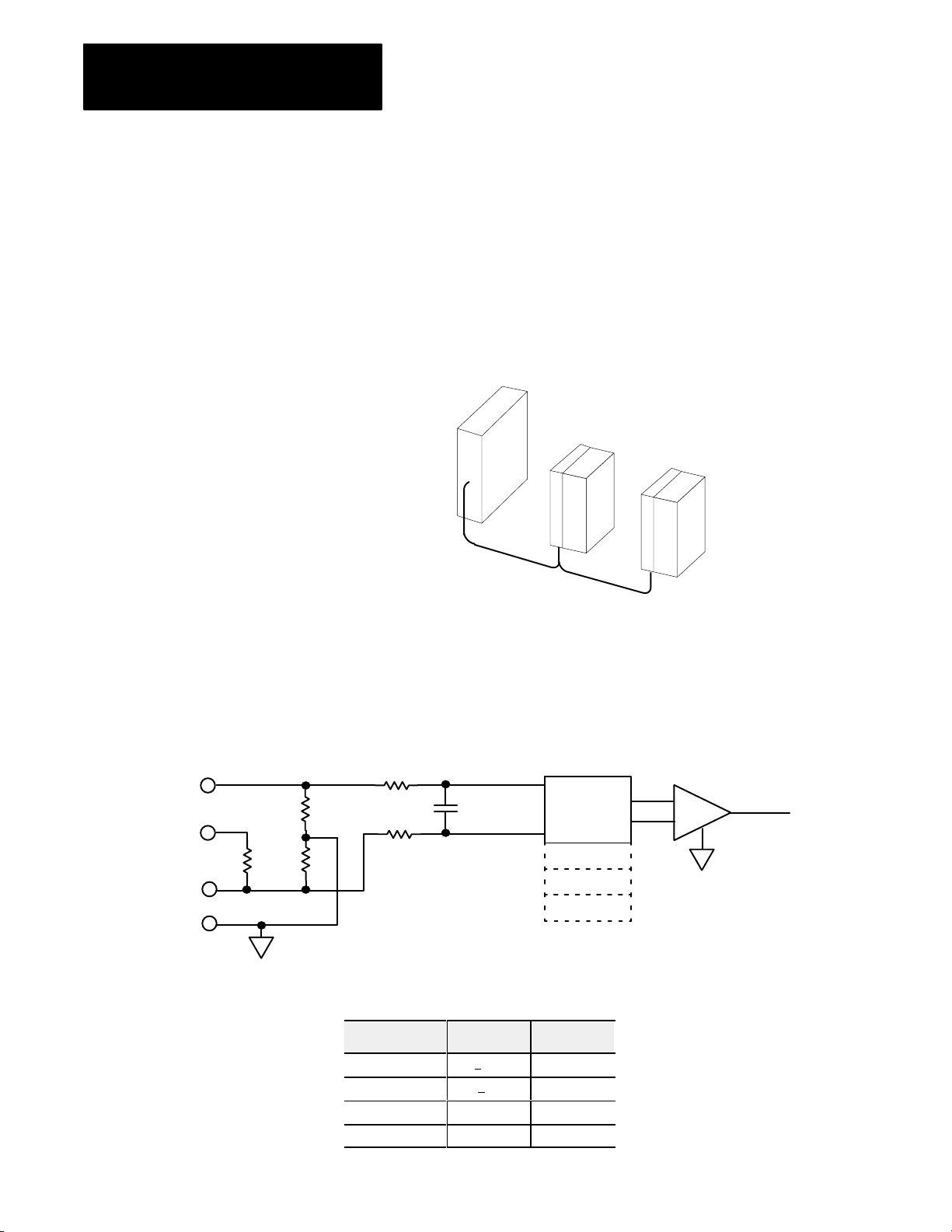
Inputs
Simplified Schematic
Channel 0 Input
inV0
inI0
249Ω
RET in0
GND in0
20MΩ
20MΩ
Analog Input
1
Common
+
= 1 I/O Rack
Blocks are daisychained to
a scanner
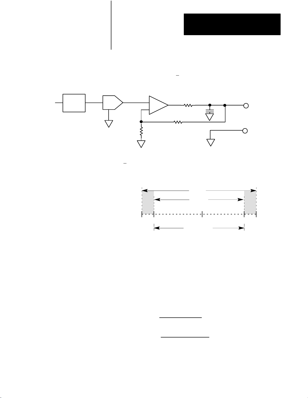
A simplified schematic of the input circuit of one input channel is
shown below.
Analog Multiplexer
ATTENTION: The 249 ohm
input current shunt is rated at
0.25 Watts. Do not exceed this
power rating or apply more
than 6V across the resistor
Channel 0
Channel 1
Channel 2
Channel 3
Instrumentation
Amplifier
+
-
Analog Input
1
Common
10828I
A/D
12501-I
1-4
Inputs have selectable input ranges as shown below.
Application Input Range Resolution
voltage +10V 14 Bits
voltage or current +5V 14 Bits
voltage 0 to 10V 14 Bits
voltage or current 0 to 5V 14 Bits
Page 12
Chapter 1
Introducing Block I/O
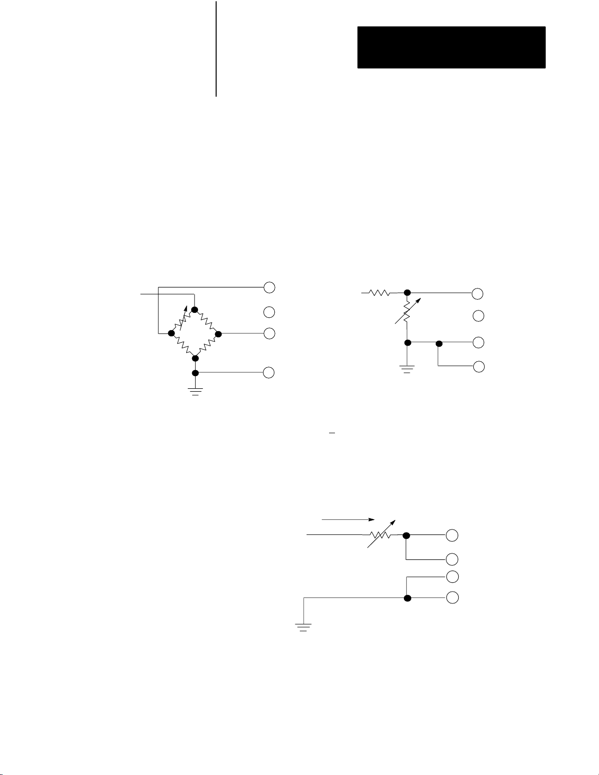
Voltage Input
Voltage inputs can be either single-ended or differential. In the voltage
mode, a signal applied between inV0 and the combination of RET in0
shorted to GND in0 provides a single-ended input mode. A signal applied
between inV0 and RET in0 provides a differential input mode. The four
terminals for ground are internally connected together to form the analog
input common. In either input mode (single-ended or differential) the
common mode voltage between any input terminal and analog input
common cannot exceed 11V or unreliable operation will occur. The figures
below show examples of differential input mode and single-ended input
mode.
10V
Differential Input Mode Singleended Input Mode
inV0
inI0
(no connection)
RET in0
GND in0
10V inV0
Current Input
When using the 0–5V or +5V range, an internal precision 249Ω shunt is
provided on each input. Input current is measured when the I
terminals are connected together. To get the proper input voltages, you
must indicate that the current shunt is connected when you configure the
module at powerup. A +24V power supply is provided for two-wire
current transducers.
I
5V
Current Input
inV0
inI0
RETin0
inI0
(no connection)
RETin0
GNDin0
and V
IN
IN
GNDin0
Each range setting has a margin of 2.5% to allow for compensation of
system or calibration inaccuracies.
1-5
Page 13
Chapter 1
Introducing Block I/O
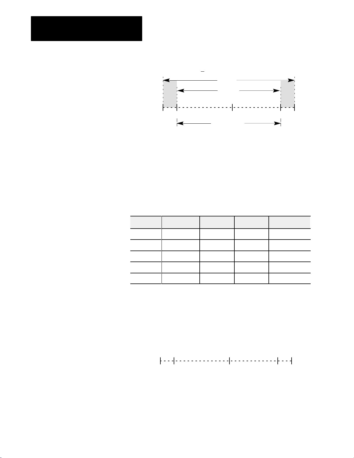
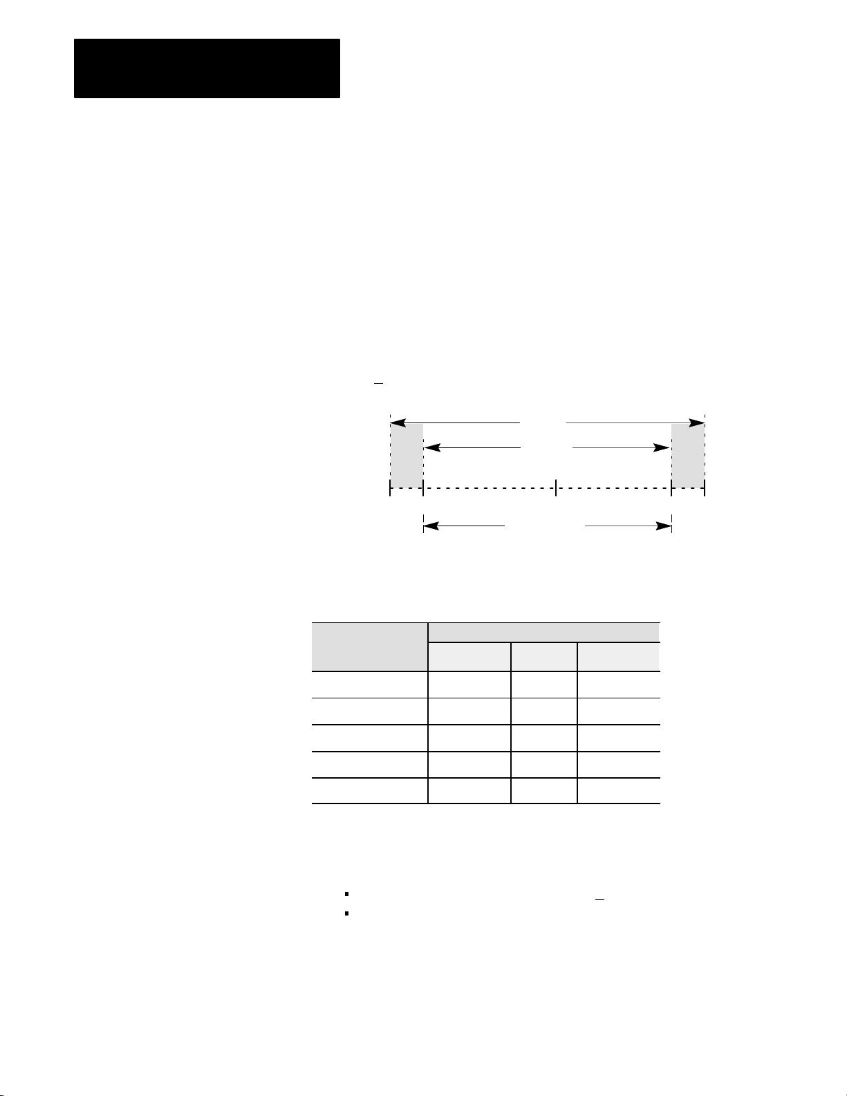
This is illustrated using the +10V scale below:
14 Bits
Resolution
Margin
13.96 Bits
Margin
Input Signal
I1 I2 I3 I4 I5
Nominal Range
In the above scale, input signals 1 thru 5 produce corresponding internal
analog to digital converter (ADC) binary counts. A full scale (FS) voltage
input produces an internal count of 16383 (input signal 1), while a bottom
scale (BS) voltage input produces an internal count of 0000 (input 5).
During calibration, the module’s representation of the counts are adjusted
so a voltage of nominal full scale (NFS) will produce a count shown as
input signal 2 while the nominal bottom scale voltage (NBS) produces a
count shown as input signal 4. For each range scale, the input voltage
which produces the ADC count of input signals 1 thru 5 in the above scale
are shown below:
Input Signal +/-10V 0-10V +/-5V 0-5V
I1 10.25V (FS) 10.25V (FS) 5.125V (FS) 5.125V (FS)
I2 +10.000V (NFS) 10.00V (NFS) 5.000V (NFS) 5.000V (NFS)
I3 0.000V 5.00V 0.000V 2.500V
I4 -10.000V (NBS) 0.00V (NBS) -5.000V (NBS) 0.000V (NBS)
I5 -10.25V (BS) -0.25V (BS) -5.125V (BS) -0.125V (BS)
Scaling
1-6
The input data represented at the module is always the internal ADC binary
counts scaled by values set in the maximum (S
) and minimum (S
max
min
)
scaler value using a two point scaling method. The input voltage which
produces input signal 2 (V
signal 4 (V
Scaling
Input Signal
Voltage
) is equal to S
nbs
Smax
I1 I2 I3 I4 I5
Vnfs
) is always equal to S
nfs
as shown below:
min
, and voltage of input
max
Smin
Vnbs
Page 14

Chapter 1
Introducing Block I/O
The following equation shows how the module interprets the input data:
Module
where:
data = M x Vin + B
– S
(S
M =
B =
(V
(S
max
nfs
min
– V
x V
(V
min
nbs
nfs
nfs
)
) – (S
)
– V
nbs
max
)
x V
nbs
)
You can choose one of three scaling methods:
binary counts (module sets scalers)
default scaling (module sets scalers)
user scaling (you set scalers)
User scaling is not available when you select discrete transfer mode.
Binary Counts Scaling
Binary counts scaling mode activates when the module powers up. This
mode guarantees the maximum resolution. The module sets the scalers as
shown in the following table:
Scaler +/-10V 0-10V +/-5V 0-5V
S
max
S
min
8191 16383 8191 16383
-8192 0 -8192 0
Default Scaling
Default scaling mode scales inputs to the input stimulus in either millivolts
or microamps. The module sets the scalers as shown in the following
tables:
With Voltage Input Selected
Scaler +/-10V 0-10V +/-5V 0-5V
S
S
With Current Input Selected
Scaler +/-10V 0-10V +/-5V 0-5V
S
S
10,000mV 10,000mV 5000mV 5000mV
max
-10,000mV 0mV -5000mV 0mV
min
max
min
N/A N/A 20000uA 20000uA
N/A N/A -20000uA 0uA
1-7
Page 15
Chapter 1
Introducing Block I/O
User Scaling
User scaling is available only when using the block transfer mode. This
mode allows you to define S
max
and S
in engineering units in the block
min
transfer write data table. The integer range is 32,767 to –32,768.
Important: If the range of user scaling values is set less than the range of
binary counts scaling values, input resolution is sacrificed.
Scaling Example
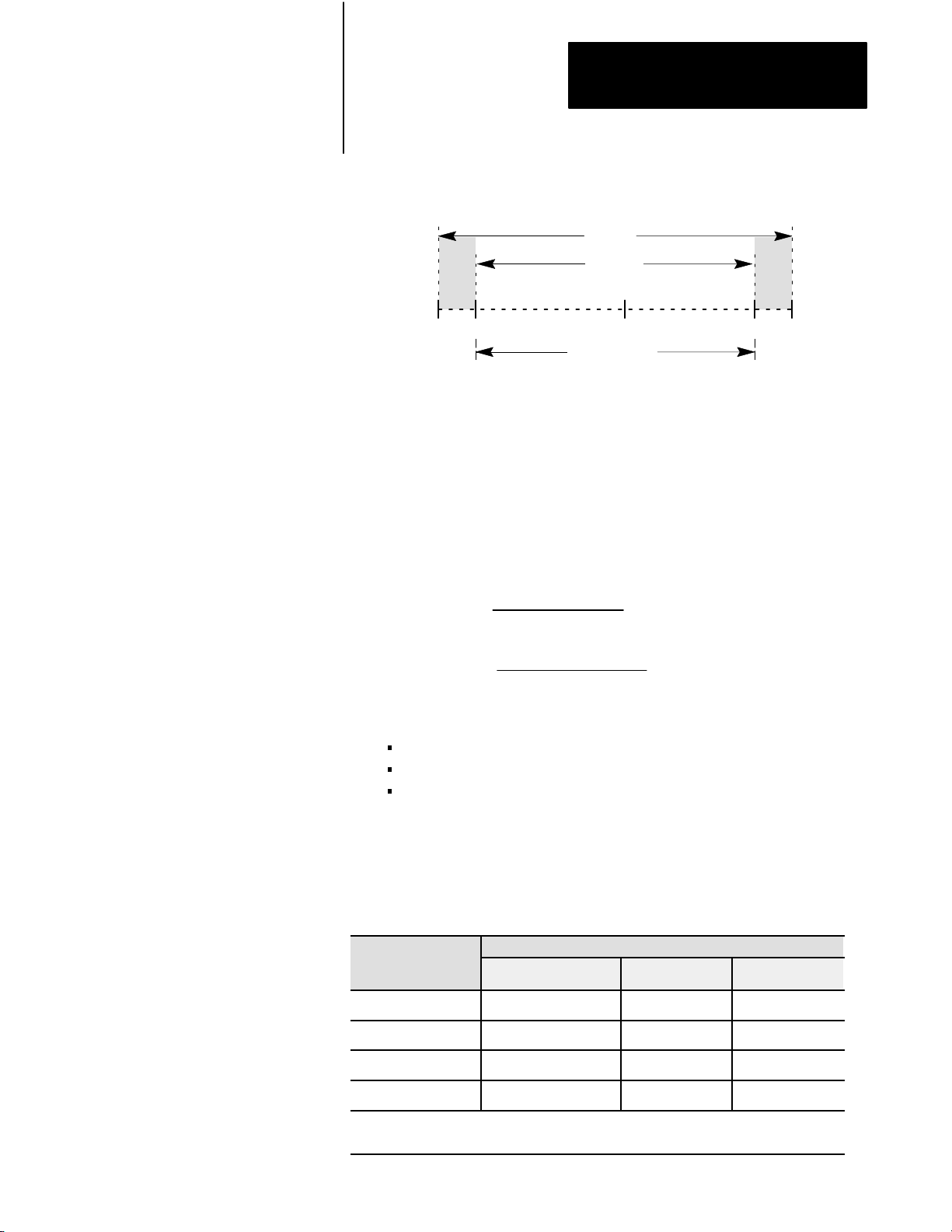
Using the +10V range scale, the following illustration shows five possible
input signals.
14 Bits
Resolution
Margin
13.96 Bits
Margin
Outputs
Input Signal
10.25 10 0 -10 -10.25
Nominal Range
The following table shows how the five signals will be scaled using each
of the three scaling methods. In the user scaling column, the S
to represent 5000 and the S
Input Value
Approx. +10.25V 8395 10250 5062
+10.000V 8191 10000 5000 (Smax)
0.000V 0000 00000 2500
-10.000V -8192 -10000 0000 (Smin)
Approx. -10.25V -8396 -10250 -0062
Binary Counts Default User
was set to represent 0.
min
Scaling Method
max
was set
The type of output your block I/O module has depends on its catalog
number:
1791-N4V2 and 1791-NDV have two +10V voltage outputs
1791-N4C2 and 1791-NDC have two 0-20mA current outputs
1-8
For any of the above modules, if your program tries to write a value which
is outside the output range, the output will be clamped at either the
maximum or minimum value. This condition will be indicated in the block
transfer read status word.
Page 16
V
OUTS
Digital
Output
Opto
Isolation
Isolated Analog
Output Common
Chapter 1
Introducing Block I/O
V
oltage Outputs - 1791N4V2 and 1791NDV
A simplified schematic of a +10V output channel is shown below.
Precision
Operational
Amplifier
DAC
2
+
-
2
V
OUT
V
RET
Note: Schematic does not show overvoltage protection circuits.
The +10V output provides 14 bits of resolution and is capable of driving
loads as small as 1k ohm. The output sacrifices a small amount of the
resolution to provide a margin of 2.5% to allow for system or calibration
inaccuracies as shown below.
Resolution
Output Signal
Scaling
The digital data sent to the output is always scaled by the values set in the
maximum (S
scaling method. When digital data sent equals S
+10.000V and the digital data sent equals S
–10.000V. The following equations shows this relationship:
Isolated Analog
2
Output Common
14 Bits
13.96 Bits
Margin
10.25 10 0 -10 -10.25
Nominal Range
) and minimum (S
max
) scaler values using a two point
min
Isolated Analog
2
Output Common
, the output produces
max
, the output produces
min
12501-I
Margin
Vout
= M x Module Data + B
where:
M =
B =
(Smax – Smin)
10 x (Smax + Smin)
(Smax – Smin)
20V
1-9
Page 17
Chapter 1
Introducing Block I/O
You can choose one of three scaling methods:
binary counts
default scaling
user scaling
User scaling is not available when you select discrete transfer mode.
The following table shows the output signals produced by various module
data values entered in each of the three scaling methods. In the user scaling
column, S
Output Signal
Approx. +10.25V 8395 10250 5062
was set to 5000 and S
max
Binary Counts
Scaling
was set to 0000.
min
Module Data
Default
Scaling
User
Scaling
+10V 8191 10000 5000 (Smax)
0.000V 0000 00000 2500
-10.00V -8192 -10000 0000 (Smin)
Approx. -10.25V -8396 -10250 -0062
Current Outputs - 1791N4C2 and 1791NDC
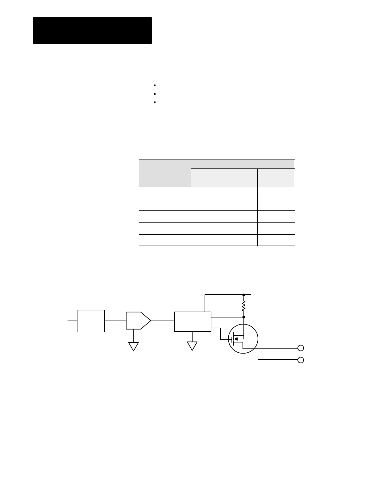
A simplified schematic of a 0 to 20mA output channel is shown below.
I
OUTS
Digital
Output
Note: Schematic does not show overvoltage protection circuits.
Opto
Isolation
Isolated Analog
Output Common
DAC
2
Isolated Analog
Output Common
High Side
Current
Monitor
2
+15V
-15V
I
OUT
I
RET
12505-I
1-10
The 0 to 20mA output provides 13 bits of resolution and is capable of
driving loads as large as 1k ohm.
Page 18
Chapter 1
Introducing Block I/O
The output sacrifices a small amount of the resolution to provide a margin
of 2.5% to allow for system or calibration inaccuracies as shown below.
13 Bits
Resolution
Margin
12.9 Bits
Margin
Input Signal
20.5 20 10 0.0 –0.5
Nominal Range
Scaling
The digital data sent to the output is always scaled by the values set in the
maximum (S
scaling method. When digital data sent equals S
20.000mA and the digital data sent equals S
0.000mA. The following equations shows this relationship:
Iout
where:
You can choose one of three scaling methods:
binary counts
default scaling
user scaling
) and minimum (S
max
= M x Module Data + B
M =
B =
(Smax – Smin)
20mA x (Smax + Smin)
(Smax – Smin)
min
20mA
) scaler values using a two point
, the output produces
max
, the output produces
min
User scaling is not available when you select discrete transfer mode.
The following table shows the output signals produced by various module
data values entered in each of the three scaling methods. In the user scaling
column, S
Output Signal
Nominally +20.5mA 8395 10250 5062
20.000mA 8191 10000 5000 (Smax)
0.000mA 0000 00000 2500 (Smin)
Nominally -0.5mA
1
The actual output can never go negative. However
compensation.
was set to 5000 and S
max
Binary Counts Scaling Default Scaling User Scaling
1
-0396 -00050 -2437
was set to 0000.
min
Module Data
, some of the output range is used to allow for zero of
fset
1-11
Page 19

Installing Block I/O
1771SN
14 blocks with 150 ohm terminator
PLC2 famil
1772SD, 1772SD2
16 blocks/channel, 28 blocks/scanner
A
PLC3
with 150 ohm terminator. 128 blocks
32 blocks/channel, 64 blocks/scanner
with 2 scanners, 82 ohm terminator
PLC
Chapter
2
Chapter
Objectives
Preinstallation
Considerations
When using and Maximum Capacity
y
In this chapter, you will learn how to mount the block, connect the remote
I/O link, connect the input and output wiring to the block, and terminate
the remote I/O link.
Before installation, you must determine the:
scanner/processor to use
number of blocks on your network
throughput requirements
total distance of the installation
transmission rate desired
external fuses required (if any)
Acceptable combinations are shown in Table 2.A.
Table 2.A
Acceptable
Combinations of Processor and Block I/O
Baud Rate
14 blocks with 150 ohm terminator
and discrete transfer
16 blocks/channel, 28 blocks/scanner
with 150 ohm terminator
57.6K 10,000 cablefeet
115.2K 5,000 cablefeet
57.6K 10,000 cablefeet
115.2K 5,000 cablefeet
Used
Maximum
Network Distance
PLC3 family
5 family
ny
1775S5, or SR5 module
PLC5VME (6008LTV)
PLC5/11
scanner module
16 blocks/channel, 64 blocks/scanner
with 150 ohm terminator. 128 blocks
with 2 scanners and 150 ohm
terminator.
32 blocks/channel, 64 blocks/scanner
with 82 ohm terminator. 128 blocks
with 2 scanners, 82 ohm terminator
and extended node addressing.
4 blocks with 150 ohm terminator
4 blocks with 150 ohm terminator
57.6K 10,000 cablefeet
115.2K 5,000 cablefeet
57.6K 10,000 cablefeet
115.2K 5,000 cablefeet
230.4K 2,000 cablefeet
57.6K 10,000 cablefeet
57.6K 10,000 cablefeet
115.2K 5,000 cablefeet
230.4K 2,500 cablefeet
2-1
Page 20
Chapter 2
terminator
16 blocks/channel, 28 blocks per
28 blocks/ch
16 blocks/channel, 60 blocks per
32 blocks/ch
16 blocks/channel, 32 blocks per
32 blocks/ch
16 blocks/channel, 64 blocks per
32 blocks/ch
16 blocks/channel, 32 blocks per
32 blocks/ch
Installing Block I/O
PLC5 family (continued)
PLC5/15
PLC5/20
PLC5/25
PLC5/30
PLC5/40
Maximum CapacityandWhen using
1
12 blocks with 150 ohm terminator 57.6K 10,000 cablefeet
Baud Rate
Used
Maximum
Network Distance
57.6K 10,000 cablefeet
12 blocks with 82 ohm or 150 ohm
terminator
115.2K 5,000 cablefeet
230.4K 2,500 cablefeet
2
16 blocks with 150 ohm terminator,
28 blocks with 82 ohm terminator and
57.6K 10,000 cablefeet
extended node addressing
16 blocks/channel, 28 blocks per
processor with 150 ohm terminator
57.6K 10,000 cablefeet
115.2K 5,000 cablefeet
57.6K 10,000 cablefeet
annel, 28 blocks per
processor with 82 ohm terminator
115.2K 5,000 cablefeet
and extended node addressing
230.4K 2,500 cablefeet
16 blocks/channel, 60 blocks per
processor with 150 ohm terminator
57.6K 10,000 cablefeet
115.2K 5,000 cablefeet
57.6K 10,000 cablefeet
annel, 60 blocks per
processor with 82 ohm terminator
115.2K 5,000 cablefeet
and extended node addressing
230.4K 2,500 cablefeet
PLC5/40L
PLC5/60
PLC5/60L
16 blocks/channel, 32 blocks per
processor with 150 ohm terminator
annel, 60 blocks per
processor with 82 ohm terminator
and extended node addressing
16 blocks/channel, 64 blocks per
processor with 150 ohm terminator
annel, 92 blocks per
processor with 82 ohm terminator
and extended node addressing
16 blocks/channel, 32 blocks per
processor with 150 ohm terminator
annel, 64 blocks per
processor with 82 ohm terminator
and extended node addressing
57.6K 10,000 cablefeet
115.2K 5,000 cablefeet
57.6K 10,000 cablefeet
115.2K 5,000 cablefeet
230.4K 2,500 cablefeet
57.6K 10,000 cablefeet
115.2K 5,000 cablefeet
57.6K 10,000 cablefeet
115.2K 5,000 cablefeet
230.4K 2,500 cablefeet
57.6K 10,000 cablefeet
115.2K 5,000 cablefeet
57.6K 10,000 cablefeet
115.2K 5,000 cablefeet
230.4K 2,500 cablefeet
2-2
Page 21
Chapter 2
a 5 50 S e o e sca e
32 blocks/channel, 32
scanners) with 82 ohm terminator
8 block
3
Controller
Module (discrete mode only)
Installing Block I/O
Maximum CapacityandWhen using
16 blocks/channel, 32
Baud Rate
Used
57.6K 10,000 cablefeet
blocks/scanner, (128 blocks with 4
scanners) with 150 ohm terminator
PLC5 family (continued)
PLC5/250 requires
a 5150RS remote scanner
32 blocks/channel, 32
blocks/scanner, (128 blocks with 4
scanners) with 82 ohm terminator
and extended node addressing
SLC5/02 (and greater)
Controller
1747SN Remote I/O Scanner
Module (discrete mode only)
s with 150 ohm terminator
8 blocks with 82 ohm terminator
1
PLC5/15 series A and PLC5/15 series B prior to revision H (B/H) can only address 3 blocks.
2
PLC5/25 revisions prior to A/D can only address 7 blocks.
3
Analog block is 1/2 rack in discrete transfer mode. If you combine analog block and discrete transfer on the same RIO link, the capacity ranges between 8 and 15 blocks.
Installing the Block I/O
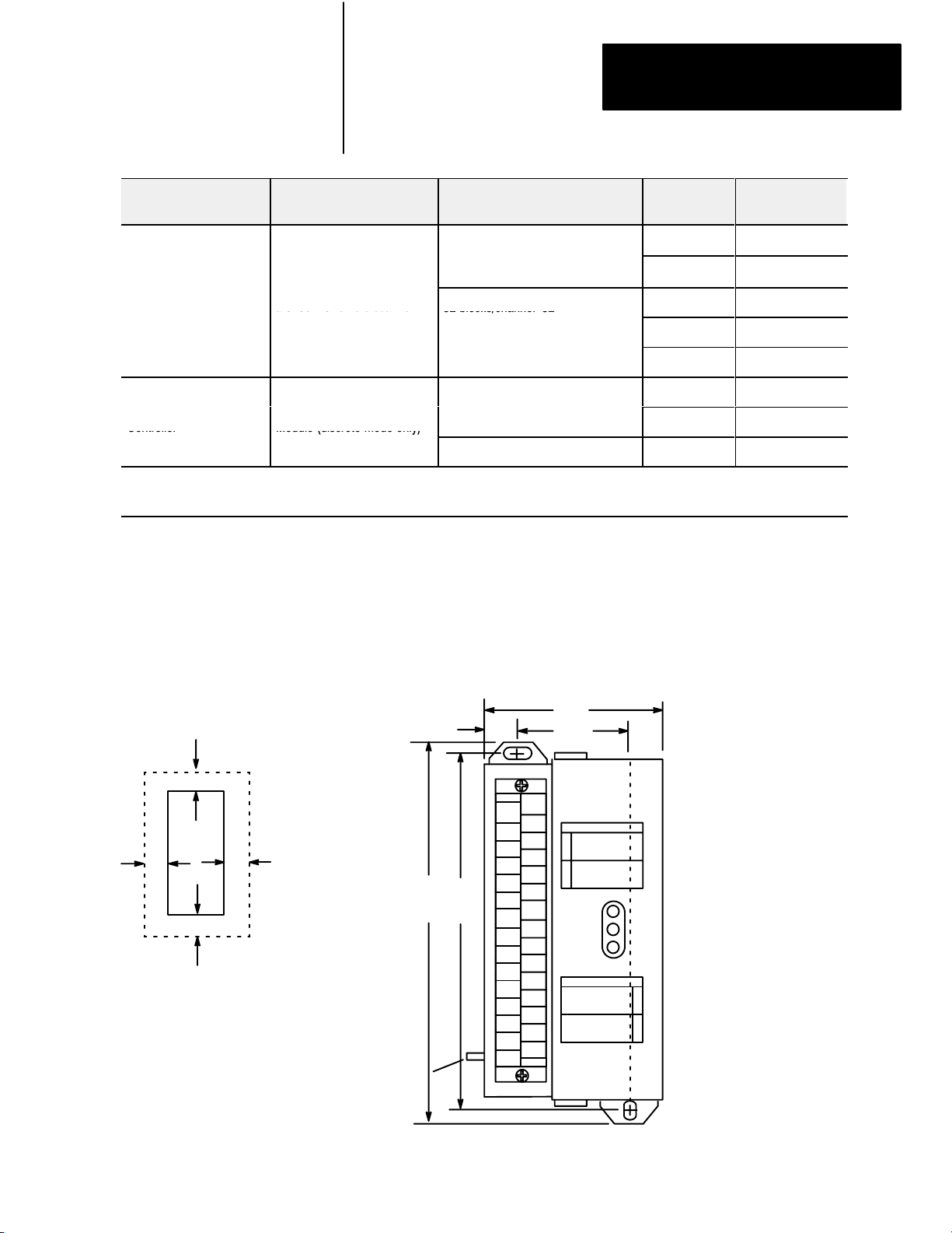
Figure 2.1 shows the mounting dimensions for the block I/O module.
115.2K 5,000 cablefeet
57.6K 10,000 cablefeet
115.2K 5,000 cablefeet
230.4K 2,500 cablefeet
57.6K 10,000 cablefeet
3
115.2K 5,000 cablefeet
3
230.4K 2,500 cablefeet
Mount the blocks vertically with a minimum of 2” between blocks. This air
gap is necessary to maintain proper cooling air flow through the block.
Maximum
Network Distance
Block
2.0 (50.8) air gap
on all 4 sides.
Operating temperature in
gap
below module must
air
not
exceed 60oC (140oF).
Figure 2.1
Mounting
Equipment
Grounding
Stud
CAUTION:
Dimensions for the Block I/O Modules (1791N4V2 shown)
2.710
1
(68.8)
1.71
(43.4)
ANALOG BLOCK
0
1
POWER
COMM
FAULT
1791N4V2
OUTPUT
INPUT
Inches
(Millimeters)
6.95H x 2.710W x 3.85D
(176.5H x 68.8W x 98D)
0
1
2
3
2 mounting holes
for 1/4inch screws
0.5
(12.7)
6.95
6.60
(176.5)
(167.6)
30
When tightening grounding stud nut, do not exceed 15 inlbs.
2-3
Page 22
Chapter 2
Installing Block I/O
Connecting Wiring
Figure 2.2
Mounting
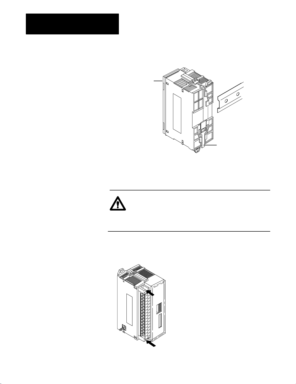
1. Hook top of slot over DIN rail.
2. While pressing block against rail,
pull down on locking lever.
3. When block is flush against rail,
push up on locking lever to
secure block to rail.
on a DIN Rail
Block
DIN Rail
AB pt. no. 199DR1
DIN 462773
EN 50022
(3.4 x 7.5mm)
Locking Lever
12382I
Make wiring connections to the removable terminal block which plugs into
the front of the block.
Figure 2.3
Removing
ATTENTION: The terminal block is not keyed to prevent
incorrect insertion. If you remove the terminal block, make
certain that it is inserted with the lower row of screws on the
outside of the block with number 1 at the top of the
terminal strip.
the T
erminal Block
To remove the terminal strip,
unscrew the two captive screws
and pull the terminal strip out.
2-4
12383I
Page 23
Chapter 2
Installing Block I/O
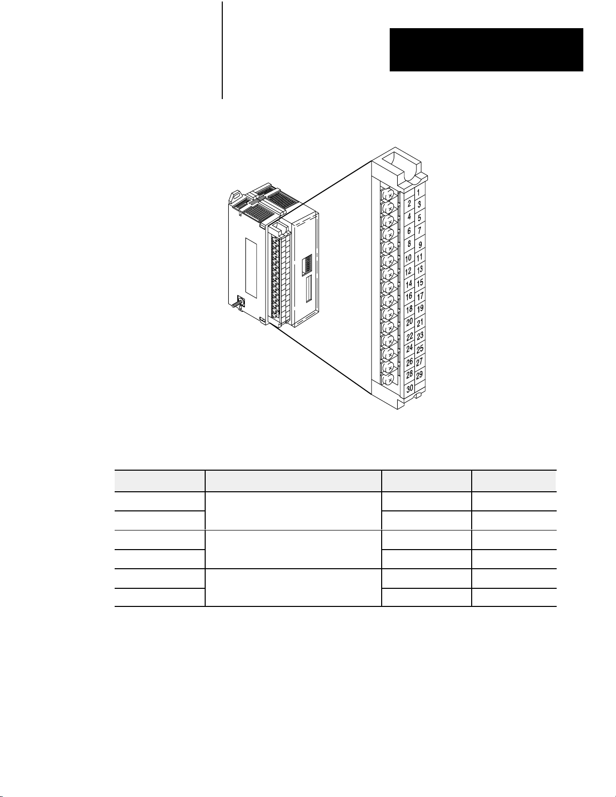
Figure 2.4
Terminal
Block Pin Numbering
Refer to the following table for wiring schematics and connecting wiring
lists for the analog block modules.
Power Supply Voltage Input For Schematic refer to: For wiring refer to:
120V ac
24V dc
120V ac
24V dc
120V ac
24V dc
Wiring Connections for the Analog Block with
Wiring Connections for the Analog Block with
Voltage Inputs
Wiring Connections for the Analog Block with
Wiring Connections for the Analog Block with
Current Input and CustomerSupplied Loop Power
Wiring Connections for the Analog Block with
Wiring Connections for the Analog Block with
Current Input and BlockSupplied Loop Power
Figure 2.5, page 26 Table 2.B, page 29
Figure 2.6, page 26 Table 2.C, page 210
Figure 2.7, page 27 Table 2.D, page 211
Figure 2.8, page 27 Table 2.E, page 212
Figure 2.9, page 28 Table 2.D, page 211
Figure 2.10, page 28 Table 2.E, page 212
2-5
Page 24
Chapter 2
Installing Block I/O
RIO
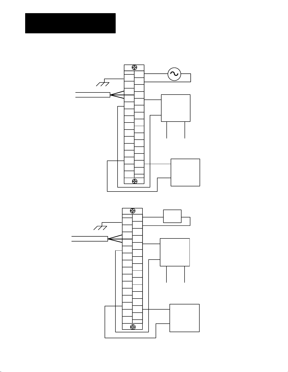
Figure 2.5
Connections for the 120V ac Analog Block with V
Wiring
GND
NOT
USED
BLU
CLR
RET
in0
GND
in0
RET
in1
GND
in1
RET
in2
GND
in2
RET
in3
GND
in3
RET
out0
RET
out1
NOT
USED
30
NOT
USED
SHD
in
in I0
in V1
in I1
in V2
in I2
in V3
in I3
+24
Vdc
out0
out1
1
L1
N
V0
L1
Voltage Input
+
User Analog
Input Device
-
User +24V User GND
Output
+
User Analog
Output Device
-
oltage Inputs
L2/N
Analog signals must be within the 10V
common mode voltage range which is
referenced to the analog input common
(GND). Typically, this is accomplished by
connecting to user ground. If an input
channel floats outside of this range,
invalid input readings will result.
RIO
Figure 2.6
Connections for the 24V dc Analog Block with V
Wiring
GND
NOT
USED
BLU
CLR
RET
in0
GND
in0
RET
in1
GND
in1
RET
in2
GND
in2
RET
in3
GND
in3
RET
out0
RET
out1
NOT
USED
30
RET
+24
NOT
USED
SHD
in
in I0
in V1
in I1
in V2
in I2
in V3
in I3
+24
Vdc
out0
out1
1
+24
V0
+
+24V dc
Supply
Voltage Input
+
User Analog
Input Device
-
User +24V User GND
Output
+
User Analog
Output Device
-
oltage Input
-
Analog signals must be within the 10V
common mode voltage range which is
referenced to the analog input common
(GND). Typically, this is accomplished by
connecting to user ground. If an input
channel floats outside of this range,
invalid input readings will result.
2-6
Page 25

RIO
Output
User Analog
Output Device
Figure 2.7
Connections for the 120V ac Analog Block with Current Input and
Wiring
CustomerSupplied Loop Power
GND
NOT
USED
BLU
CLR
RET
in0
GND
in0
RET
in1
GND
in1
RET
in2
GND
in2
RET
in3
GND
in3
-
+
RET
out0
RET
out1
NOT
USED
30
NOT
USED
SHD
in
in I0
in V1
in I1
in V2
in I2
in V3
in I3
+24
Vdc
out0
out1
Chapter 2
Installing Block I/O
1
L1
N
L1
+
V0
-
User +24V User GND
ATTENTION: The 249 ohm
input current shunt is rated
at 0.25 Watts. Do not
exceed this rating.
L2/N
Current Input
User Analog
Input Device
Analog signals must be within the
10V common mode voltage range
which is referenced to the analog
input common (GND). Typically, this
is accomplished by connecting to
user ground. If an input channel
floats outside of this range, invalid
input readings will result.
RIO
Output
User Analog
Output Device
Figure 2.8
Connections for the 24V dc Analog Block with Current Input and
Wiring
CustomerSupplied Loop Power
GND
NOT
USED
BLU
CLR
RET
in0
GND
in0
RET
in1
GND
in1
RET
in2
GND
in2
RET
in3
GND
in3
-
+
RET
out0
RET
out1
NOT
USED
30
RET
+24
NOT
USED
SHD
in
in I0
in V1
in I1
in V2
in I2
in V3
in I3
+24
Vdc
out0
out1
1
+24
V0
+
+24V dc
Supply
Current Input
+
User Analog
Input Device
-
User +24V User GND
ATTENTION: The 249 ohm
input current shunt is rated
at 0.25 Watts. Do not
exceed this rating.
-
Analog signals must be within the
10V common mode voltage range
which is referenced to the analog
input common (GND). Typically,
this is accomplished by connecting
to user ground. If an input channel
floats outside of this range, invalid
input readings will result.
2-7
Page 26

Chapter 2
Installing Block I/O
Figure 2.9
Connections for the 120V ac Analog Block with Current Input and
Wiring
BlockSupplied Loop Power
RIO
Output
User Analog
Output Device
RIO
Output
User Analog
Output Device
1
L1
GND
N
NOT
USED
NOT
USED
BLU
SHD
CLR
in
V0
RET
in0
in I0
GND
in0
in V1
RET
in1
in I1
GND
in1
in V2
RET
in2
in I2
GND
in2
in V3
RET
in3
in I3
GND
in3
+24
RET
-
+
out0
RET
out1
NOT
USED
30
Vdc
out0
out1
L1
i
i
+24V dc loop power supplied
at terminal 25 on block
ATTENTION: The 249 ohm
input current shunt is rated
at 0.25 Watts. Do not
exceed this rating.
L2/N
Loop Powered
Current Input
User Analog
Input Device
Analog signals must be within the
10V common mode voltage range
which is referenced to the analog
input common (GND). Typically, this
is accomplished by connecting to
user ground. If an input channel
floats outside of this range, invalid
input readings will result.
Figure 2.10
Connections for the 24V dc Analog Block Module with Current
Wiring
Input and BlockSupplied Loop Power
1
+24
GND
RET
+24
NOT
USED
NOT
USED
BLU
SHD
CLR
in
V0
RET
in0
in I0
GND
in0
in V1
RET
in1
in I1
GND
in1
in V2
RET
in2
in I2
GND
in2
in V3
RET
in3
in I3
GND
in3
+24
RET
-
+
out0
RET
out1
NOT
USED
30
Vdc
out0
out1
+
+24V dc
-
Supply
Loop Powered
Current Input
i
User Analog
i
Input Device
+24V dc loop power supplied
at terminal 25 on block
ATTENTION: The 249 ohm
input current shunt is rated
at 0.25 Watts. Do not
exceed this rating.
Analog signals must be within the
10V common mode voltage range
which is referenced to the analog
input common (GND). Typically, this
is accomplished by connecting to
user ground. If an input channel
floats outside of this range, invalid
input readings will result.
2-8
Page 27

Table 2.B
Power
Remote I/O
Block Designations for Cat. No. 1791N4V2
Wiring
Connections
Designation Description Terminal No.
Chapter 2
Installing Block I/O
1791-N4V2
Power
Connections
L1 ac hot 1
N
ac neutral 3
GND Chassis ground 2
Transducer
2
Power
Remote I/O
Connections
+24V For current input only 25
BLU Blue wire - RIO 6
CLR
Clear wire - RIO 8
SHD Shield - RIO 7
I/O Connections
inV0 thru inV3 Voltage Input 0 through 3 9, 13, 17, 21
Voltage Input
RET in0 thru
RET in3
Input Return 0 through 3 10, 14, 18, 22
inI0 thru inI3 Current Input 0 through 3 11, 15, 19, 23
Current Input
RET in0 thru
RET in3
Input Return 0 through 3 10, 14, 18, 22
Input Ground GNDin0GNDin3 Channels 03 ground 12, 16, 20, 24
out 0 - RET out 0
Output
out 1 - RET out 1
Not used
1
Connect
chassis ground to equipment grounding stud. These are not internally connected.
2
2028V dc (nominal 24V, 100mA)) voltage source for accommodating looppowered current transducer inputs.
3
Terminals
4
12, 16, 20, and 24 are internally connected.
T
erminals 26 and 28 internally connected together
.
Output 0 (+)
Return output 0 (-)
Output 1 (+)
Return output 1 (-)
For internal test only; not
for customer use.
4, 5, 30
26
28
27
29
1
3
4
4
2-9
Page 28

Chapter 2
Power
Remote I/O
Installing Block I/O
Table 2.C
Block Designations for Cat. No. 1791NDV
Wiring
Connections
Power
Connections
Transducer
2
Power
Remote I/O
Connections
Designation Description Terminal No.
+24 +24V dc Power 1
RET +24
GND Chassis ground 2
dc Return 3
1
+24V For current input only 25
BLU Blue wire - RIO 6
CLR
Clear wire - RIO 8
SHD Shield - RIO 7
I/O Connections
inV0 thru inV3 Voltage Input 0 through 3 9, 13, 17, 21
1791-NDV
Voltage Input
RET in0 thru
RET in3
Input Return 0 through 3 10, 14, 18, 22
inI0 thru inI3 Current Input 0 through 3 11, 15, 19, 23
Current Input
RET in0 thru
RET in3
Input Return 0 through 3 10, 14, 18, 22
Input Ground GNDin0-GNDin3 Channels 0-3 ground 12, 16, 20, 24
out 0 - RET out 0
Output
out 1 - RET out 1
Not used
1
Connect
chassis ground to equipment grounding stud. These are not internally connected.
2
2028V dc (nominal 24V, 100mA) voltage source for accommodating looppowered current transducer inputs.
3
T
erminals 12, 16, 20, and 24 are internally connected.
4
T
erminals 26 and 28 internally connected together
Output 0 (+)
Return output 0 (-)
Output 1 (+)
Return output 1 (-)
For internal test only; not
for customer use.
.
27
4
26
29
4
28
4, 5, 30
3
2-10
Page 29

Table 2.D
Power
Remote I/O
Block Designations for Cat. No. 1791N4C2
Wiring
Connections
Designation Description Terminal No.
Chapter 2
Installing Block I/O
1791-N4C2
Power
Connections
Transducer
2
Power
Remote I/O
Connections
L1 ac hot 1
N
ac neutral 3
GND Chassis ground 2
+24V For current input only 25
BLU Blue wire - RIO 6
CLR
Clear wire - RIO 8
1
SHD Shield - RIO 7
I/O Connections
inV0 thru inV3 Voltage Input 0 through 3 9, 13, 17, 21
Voltage Input
RET in0 thru
RET in3
Input Return 0 through 3 10, 14, 18, 22
inI0 thru inI3 Current Input 0 through 3 11, 15, 19, 23
Current Input
RET in0 thru
RET in3
Input Return 0 through 3 10, 14, 18, 22
Input Ground GNDin0GNDin3 Channels 03 ground 12, 16, 20, 24
out 0 - RET out 0
Output
out 1 - RET out 1
Not used
1
Connect
chassis ground to equipment grounding stud. These are not internally connected.
2
2028V dc (nominal 24V, 100mA) voltage source for accommodating looppowered current transducer inputs.
3
T
erminals 12, 16, 20, and 24 are internally connected.
4
T
erminals 26 and 28 internally connected together
.
Output 0 (+)
Return output 0 (-)
Output 1 (+)
Return output 1 (-)
For internal test only; not
for customer use.
27
4
26
29
4
28
4, 5, 30
3
2-11
Page 30

Chapter 2
Remote I/O
Installing Block I/O
Table 2.E
Block Designationsfor Cat. No. 1791NDC
Wiring
Connections
Designation Description Terminal No.
+24 +24V dc Power 1
1791-NDC
Power Connections
RET +24
dc Return 3
GND Chassis ground 2
Transducer Power
Remote I/O
Connections
2
+24V For current input only 25
BLU Blue wire - RIO 6
CLR
Clear wire - RIO 8
SHD Shield - RIO 7
I/O Connections
inV0 thru inV3 Voltage Input 0 through 3 9, 13, 17, 21
Voltage Input
RET in0 thru
RET in3
Input Return 0 through 3 10, 14, 18, 22
inI0 thru inI3 Current Input 0 through 3 11, 15, 19, 23
Current Input
RET in0 thru
RET in3
Input Return 0 through 3 10, 14, 18, 22
Input Ground GNDin0-GNDin3 Channels 0-3 ground 12, 16, 20, 24
out 0 - RET out
0
Output
out 1 - RET out
1
Not used
1
Connect
chassis ground to equipment grounding stud. These are not internally connected.
2
2028V dc (nominal 24V, 100mA) voltage source for accommodating looppowered current transducer inputs.
3
T
erminals 12, 16, 20, and 24 are internally connected.
4
T
erminals 26 and 28 internally connected together
.
Output 0 (+)
Return output 0 (-)
Output 1 (+)
Return output 1 (-)
For internal test only; not
for customer use.
1
27
4
26
29
4
28
4, 5, 30
3
2-12
Table 2.F
W
Acceptable
Remote I/O link Belden 9463
Input and output wiring Up to 14AWG (2mm2) stranded with 3/64 inch insulation
iring Cables for Block I/O Connection
Use Cable Type
Page 31

Chapter 2
Installing Block I/O
Termination Resistor
Remote I/O Link
A termination resistor must be installed on the last block in a series.
Connect the resistor as shown in Figure 2.11.
Figure 2.11
Installing
Connect termination resistor across
terminals 6 (BLU) and 8 (CLR).
Refer to Table 2.A for proper
terminator for your application.
the T
ermination Resistor
Termination
Resistor
BLU
CLR
SHD
10835I
Blocks must be wired in series as shown in Figure 2.12 or Figure 2.13. Do
not attempt to wire any block in parallel.
The number of blocks used depends not only on the user requirements but
also on the system used. Refer to Table 2.A (page 2-1) for maximum
block usage for individual systems.
Figure 2.12
Connection for Block I/O Using PLC2, PLC3 or PLC5 Family
Series
Programmable Controllers
To Programmable
Controller or I/O
Scanner Module
Install terminating resistor on last block.
1 I/O Rack
1 I/O Rack
1 I/O Rack
1 I/O Rack
10833I
2-13
Page 32

Chapter 2
Installing Block I/O
To 1747SN
Scanner Module
Figure 2.13
Configurations for Block I/O Using the SLC Programmable
Series
Controller
1
2
7
8
Up to 8 blocks with
SLC5/02
Extended Node Capability
Install terminating resistor
on last block.
10834I
If this is the last remote I/O adapter on the remote I/O link in a PLC
system, you must use a terminating resistor to terminate both ends of the
remote I/O link (scanner end and last block end). The size of the terminator
is determined by the system configuration.
Older system configurations must use a 150 ohm resistor at both ends.
With newer devices that can support it, you can use an 82 ohm termination
resistor at both ends. The 82 ohm terminators provide “extended node”
capability which allows you to have up to 32 physical devices on the
remote I/O link. (The number of logical racks capable of being addressed
by the scanner is not affected.)
ATTENTION: Devices that are operating at 230.4K baud must
have 82 ohm terminators in place for proper operation.
2-14
Page 33

Chapter 2
Installing Block I/O
Compatibility
of 1771 I/O
Products with Extended
Node Numbers
Certain products are not compatible with extended node capabilities
obtained with the use of 82 ohm terminators. Table 2.G lists those products
that are not compatible.
Table 2.G
Noncompatible
Scanners
Adapters 1771AS All
Miscellaneous 1771AF All
Products
Device Series
1771SN All
1772SD All
1772SD2 All
1775SR All
1775S4A All
1775S4B All
1771ASB Series A
1771DCM All
1771AF1 All
Selecting Remote I/O Link Speed
The remote I/O link can operate at three speeds: 57.6K, 115.2K or 230.4K
bits/s. The selection of link speed is dependent on the scanner/processor
used, throughput requirements, distance required and the type of remote
I/O devices being used.
Throughput Requirements
Block throughput using analog block is dependent on the controllers data
transfer rate. Analog block outputs are updated within 10ms of receiving
output data from the controller. The analog block inputs are sampled in a
“round robin” fashion with an input channel sampled every 27ms. This
means that a given input channel is sampled every 108ms (four input
channels times 27ms). At the end of every sample period of 27ms, the most
recent input data is made available for data transfer to the controller.
Consult your programmable controller user manual for Remote I/O
Communications to determine your system throughput.
2-15
Page 34

Chapter
3
Configuring Your Block I/O for PLC Family
Programmable Controllers
Chapter
Setting the Configuration Switches
Objectives
In this chapter, you will learn how to configure your block I/O when used
with PLC family programmable controllers. This includes the following:
setting the configuration switches
addressing the block I/O
Each block I/O module has two 8-position switches for setting:
starting I/O group
I/O rack number
communication rate
last chassis
last state
block transfer/discrete transfer
processor restart/lockout
These switches are accessible by opening the clear plastic door on the front
of the module (Figure 3.1).
ATTENTION: Recycle power to the block I/O module after
setting the switches.
3-1
Page 35

Chapter 3
Configuring Your Block I/O for PLC
Family Programmable Controllers
1
Figure 3.1
Settings for the Analog Block I/O Modules
Switch
1791N4V2
ANALOG
BLOCK
SW2-8
Not used
87654321
SW2-7
Not Used
30
Open clear front
cover to access
switches
POWER
COMM
FAULT
SW2
01
SW1
01
Position = 1Position = 0
End View of Switch
87654321
SW2-6 Last I/O Group
0 Not last rack
1 Last rack
SW2-5
Processor
Restart/Lockout (PRL)
0 Processor Restart
1 Processor Lockout
SW2-4 Hold Last State
0 Reset Outputs
1 Hold Last State
SW2-3 Transfer Type
0 Block Transfer
1 Discrete Transfer
Communication Rate
SW2-2 SW2-1 Bits/s
3-2
ATTENTION: Recycle power to the block I/O module
after setting the switches.
0 0 57.6 K
0 1 115.2 K
1 0 230.4 K
1 1 230.4 K
Starting Quarter
SW1-2 SW1-1
0 0 0 (1st)
0 1 2 (2nd)
1 0 4 (3rd)
1 1 6 (4th)
Module
Group
Page 36

Chapter 3
Configuring Your Block I/O for PLC
Family Programmable Controllers
1747SN
Rack
Number
Rack
Rack 1 Rack 2 Rack 2 Rack 1 Rack 1 Rack 1
Rack 2 Rack 3 Rack 3 Rack 2 Rack 2 Rack 2
Rack 3 Rack 4 Rack 4 Rack 3 Rack 3 Rack 3
1771SN
Rack
Number
0
Rack 1 Rack 1
Rack 5 Rack 5 Rack 4 Rack 4 Rack 4
Rack 6 Rack 6 Rack 5 Rack 5 Rack 5
Rack 7 Rack 7 Rack 6 Rack 6 Rack 6
PLC2
Rack
Number
PLC5
Rack
Number
Not V
Rack 7 Rack 7 Rack 7
Rack 10 Rack 10 Rack 10
Rack 1
Rack 12 Rack 12 Rack 12
Rack 13 Rack 13 Rack 13
Rack 14 Rack 14 Rack 14
Rack 15 Rack 15 Rack 15
Rack 16 Rack 16 Rack 16
Rack 17 Rack 17 Rack 17
Rack 20 Rack 20 Rack 20
Rack 21 Rack 21 Rack 21
Rack 22 Rack 22 Rack 22
Rack 23 Rack 23 Rack 23
Rack 24 Rack 24 Rack 24
Rack 25 Rack 25 Rack 25
Rack 26 Rack 26 Rack 26
Rack 27 Rack 27 Rack 27
PLC5/250
Number
alid
1
Rack 1
Rack 30 Rack 30
Rack 31 Rack 31
Rack 32 Rack 32
Rack 33 Rack 33
Rack 34 Rack 34
Rack 35 Rack 35
Rack 36 Rack 36
Rack 37 Rack 37
Rack
Rack 0 Rack 0
PLC3
Rack
Number
1
Rack 1
Rack 40
Rack 41
Rack 42
Rack 43
Rack 44
Rack 45
Rack 46
Rack 47
Rack 50
SW1 Switch Position
8 7 6 5 4 3
0 0 0 0 0 0
0 0 0 0 0 1
0 0 0 0 1 0
0 0 0 0 1 1
0 0 0 1 0 0
0 0 0 1 0 1
0 0 0 1 1 0
0 0 0 1 1 1
0 0 1 0 0 0
1 0 0 1 0 0 1
0 0 1 0 1 0
0 0 1 0 1 1
0 0 1 1 0 0
0 0 1 1 0 1
0 0 1 1 1 0
0 0 1 1 1 1
0 1 0 0 0 0
0 1 0 0 0 1
0 1 0 0 1 0
0 1 0 0 1 1
0 1 0 1 0 0
0 1 0 1 0 1
0 1 0 1 1 0
0 1 0 1 1 1
0 1 1 0 0 0
0 1 1 0 0 1
0 1 1 0 1 0
0 1 1 0 1 1
0 1 1 1 0 0
0 1 1 1 0 1
0 1 1 1 1 0
0 1 1 1 1 1
1 0 0 0 0 0
1 0 0 0 0 1
1 0 0 0 1 0
1 0 0 0 1 1
1 0 0 1 0 0
1 0 0 1 0 1
1 0 0 1 1 0
1 0 0 1 1 1
1 0 1 0 0 0
3-3
Page 37

Chapter 3
Configuring Your Block I/O for PLC
Family Programmable Controllers
1747SN
1747SN
Rack
Rack
Number
Number
Rack
address 77 is an illegal configuration.
PLC5/1
PLC5/15 and PLC5/20 processors can scan racks 0103.
PLC5/25 and PLC5/30 processors can scan racks 0107.
PLC5/40 and PLC5/40L processors can scan racks 0117.
PLC5/60 and PLC5/60L processors can scan racks 0127.
PLC5/250 processors can scan racks 037.
PLC3 processors can scan racks 076.
1771SN
1771SN
Rack
Rack
Number
Number
1 processors can scan rack 03.
PLC2
PLC2
Rack
Rack
Number
Number
PLC5
PLC5
Rack
Rack
Number
Number
PLC5/250
PLC5/250
Rack
Rack
Number
Number
PLC3
PLC3
Rack
Rack
Number
Number
Rack
51
Rack 52
Rack 53
Rack 54
Rack 55
Rack 56
Rack 57
Rack 60
Rack 61
Rack 62
Rack 63
Rack 64
Rack 65
Rack 66
Rack 67
Rack 70
Rack 71
Rack 72
Rack 73
Rack 74
Rack 75
Rack 76
Not V
alid 1 1 1 1 1 1
SW1 Switch Position
1 0 1 0 0 1
1 0 1 0 1 0
1 0 1 0 1 1
1 0 1 1 0 0
1 0 1 1 0 1
1 0 1 1 1 0
1 0 1 1 1 1
1 1 0 0 0 0
1 1 0 0 0 1
1 1 0 0 1 0
1 1 0 0 1 1
1 1 0 1 0 0
1 1 0 1 0 1
1 1 0 1 1 0
1 1 0 1 1 1
1 1 1 0 0 0
1 1 1 0 0 1
1 1 1 0 1 0
1 1 1 0 1 1
1 1 1 1 0 0
1 1 1 1 0 1
1 1 1 1 1 0
345678
3-4
The SLC 500 controllers communicate with the block I/O using an I/O
Scanner module (cat. no. 1747-SN series A). Refer to the user manual for
the 1747-SN/A Scanner module for more information.
Note: These block I/O modules are not compatible with the 1747-DSN
Distributed I/O Scanner module.
Page 38

Block transfer requires 1/4 rack.
Chapter 3
Configuring Your Block I/O for PLC
Family Programmable Controllers
When using block transfer, each analog block I/O module uses 2 words of
output image table memory and 2 words of input image table memory.
Each block occupies 1/4 rack of data table, with 4 blocks comprising 1
logical rack. Image table usage for one assigned rack number is shown in
Figure 3.3.
Figure 3.2
Image T
I/O
1791N4C2
MSB = Module Status Byte
MCB = Module Control Byte
able for One Assigned Rack Number using Block T
Input Image
0
1
2
3
4
5
6
7
1791N4C2
0
1
2
3
4
5
6
7
MSB
Reserved
MSB
Reserved
Output Image
710
MCB
Reserved
MCB
Reserved
ransfer
PLC
017 710
1/4 Rack
1/4 Rack
PLC
017
1/4 Rack
1/4 Rack
3-5
Page 39

Chapter 3
Configuring Your Block I/O for PLC
Family Programmable Controllers
Discrete transfer requires 1/2 rack.
1791N4C2
When using discrete transfer, each analog block I/O module uses 4 words
of output image table memory and 4 words of input image table memory.
Each block occupies 1/2 rack of data table, with 2 blocks comprising 1
logical rack. Image table usage for one assigned rack number is shown in
Figure 3.3.
Figure 3.3
Image Table for One Assigned Rack Number using Discrete T
I/O
Input Image
0
1
2
3
4
5
6
7
1791N4C2
0
1
2
3
4
5
6
7
Input 0
Input 1
Input 2
Input 3
Input 0
Input 1
Input 2
Input 3
Output Image
710
Configuration
Output 0
Output 1
Reserved
Configuration
Output 0
Output 1
Reserved
ransfer
017 710
1/2 Rack
017
SLC 50007815
PLC
1/2 Rack
SLC 50007815
PLC
1/2 Rack
1/2 Rack
3-6
Page 40

Chapter 3
Configuring Your Block I/O for PLC
Family Programmable Controllers
Module
Scan T
ime
Scan time depends on the block transfer rate over the remote I/O network,
which is asynchronous to the module input sample rate and output update
rate. The block transfer rate is dependent on the controller, program length,
the amount of communication traffic to other modules on the remote I/O
network and the speed (baud rate) of the remote I/O network.
Figure 3.4
Scan Time Relationships
Module
Block Transfer
Read
Input Sample
Rate
Block Transfer
Write
Output Update
1
Time depends on the remote I/O network configuration.
BTR1
108ms
Ch 0 Ch 1 Ch 2 Ch 3 Ch 0 Ch 1 Ch 2 Ch 3 Ch 0 Ch 1
BTW1
10ms 10ms
Ch 0 & Ch 1
updated
100ms to 2s
100ms to 2s
1
BTR2
1
BTW2
Ch 0 & Ch 1
updated
3-7
Page 41

Chapter
4
Analog Block Applications Using
Block Transfers
Chapter
Objectives
Reading Data and Status from the Module
Block Transfer Read Data Format
In this chapter, you will read about:
reading data and status from the module
block transfer read data format
configuring the module and setting outputs with block transfer
write instructions
Block transfer instructions are used when the analog block is used with
PLC programmable controllers with block transfer capability. Block
transfer read (BTR) programming moves status and data from the module
to the processor’s data table in one I/O scan. The processor user program
initiates the request to transfer data from the module to the processor.
The transferred words contain module status, channel status and input data
from the module. The maximum BTR data file length required is five
words (0 thru 4).
The block transfer read data format consists of input data and module
status. Word 0 contains the power up bit (PU), the bad configuration bit
(BC), out of range bit (OR), status code, high alarm and low alarm bits.
Words 1 through 4 contain input channel data.
Complete configuration data and bit/word descriptions are shown in
Figure 4.1 and Table 4.A.
Figure 4.1
T
ransfer Read for Analog Blocks using PLC Controllers
Block
Decimal 15 14 13 12 11 10 09 08 07 06 05 04 03 02 01 00
Octal 17 16 15 14 13 12 11 10 07 06 05 04 03 02 01 00
0 PU BC OR Status Code High Alarm Low Alarm
1 Input Channel 0 Data
2 Input Channel 1 Data
3 Input Channel 2 Data
4 Input Channel 3 Data
4-1
Page 42

Chapter 4
Analog Block Applications Using
Block Transfers
Word
Word 0
Table 4.A
Bit/Word
Decimal
(Octal Bit)
Bits 15 (17)
Bit 14 (16)
Bit 13 (15)
Bits 0812
(1014)
Descriptions for Block Transfer Read Instruction
Bit
Power up (PU) status bit. This bit is set (1) if the module has not been
configured since the last power up. It is reset (0) when at least one valid BTW
has occurred since power up. Outputs are not enabled until the PU bit is reset.
Bad configuration (BC) bit. This bit is set (1) if an invalid configuration data has
been received, and the previous configuration remains in effect.
Out of range (OR) bit. When set, indicates one or both of the outputs has
received a value which exceeds the output range. Outputs are clamped at their
maximum or minimum values depending on the direction of the out of range
value.
Status Codes. When the Bad Configuration (BC) bit 14 (16), is set (1), the
status code indicates the following:
1 output channel 0 scaling error
2 output channel 1 scaling error
3 input channel 0 scaling error
4 input channel 1 scaling error
5 input channel 2 scaling error
6 input channel 3 scaling error
7 channel 0 alarm error
8 channel 1 alarm error
9 channel 2 alarm error
A channel 3 alarm error
When the output out of range (OR) bit 13 (15) is set (1), the status code bits
indicate the following:
Bit 08 (10) output 0 has been clamped at its minimum
Bit 09 (11) output 1 has been clamped at its minimum
Bit 10 (12) output 0 has been clamped at its maximum
Bit 11 (13) output 1 has been clamped at its maximum
Description
4-2
Word 1
Word 2
Word 3
Word 4
Bits 0407
Bits 0003
Bits 0015
(0017)
Bits 0015
(0017)
Bits 0015
(0017)
Bits 0015
(0017)
High alarm bits. Set (1) if the input channel value is greater than the
corresponding high alarm value.
Bit 04 high alarm bit for channel 0
Bit 05 high alarm bit for channel 1
Bit 06 high alarm bit for channel 2
Bit 07 high alarm bit for channel 3
Low alarm bits. Set (1) if the input channel value is less than the corresponding
low alarm value.
Bit 00 low alarm bit for channel 0
Bit 01 low alarm bit for channel 1
Bit 02 low alarm bit for channel 2
Bit 03 low alarm bit for channel 3
Input data for channel 0.
Input data for channel 1.
Input data for channel 2.
Input data for channel 3.
Page 43

Chapter 4
Analog Block Applications Using
Block Transfers
Configuring the Module and
Setting Outputs with Block
ransfer W
T
rite Instructions
You must configure your block module by performing a block transfer
write (BTW) instruction from the programmable controller to the module.
Each input can be independently configured in one BTW.
Maximum length of the BTW is 27 words (0 thru 26). When configuring
the module, first send the complete BTW. You can shorten the BTW to 3
words for subsequent write operations if parameters for each channel
remain the same.
Block transfer write data is shown in Figure 4.2.
Figure 4.2
T
ransfer W
Block
Decimal 15 14 13 12 11 10 09 08 07 06 05 04 03 02 01 00
Octal 17 16 15 14 13 12 11 10 07 06 05 04 03 02 01 00
0 Module Mode Scaling Range Alarm Enable Filter
1 Output Channel 0 Data
2 Output Channel 1 Data
3 Output Channel 0 Minimum Scaling
4 Output Channel 0 Maximum Scaling
5 Output Channel 1 Minimum Scaling
6 Output Channel 1 Maximum Scaling
7 Input Channel 0 Minimum Scaling
8 Input Channel 0 Maximum Scaling
9 Input Channel 1 Minimum Scaling
10 Input Channel 1 Maximum Scaling
11 Input Channel 2 Minimum Scaling
12 Input Channel 2 Maximum Scaling
13 Input Channel 3 Minimum Scaling
14 Input Channel 3 Maximum Scaling
15 Input Channel 0 Low Alarm Level
16 Input Channel 0 High Alarm Level
17 Input Channel 0 Alarm Deadband
18 Input Channel 1 Low Alarm Level
19 Input Channel 1 High Alarm Level
20 Input Channel 1 Alarm Deadband
21 Input Channel 2 Low Alarm Level
22 Input Channel 2 High Alarm Level
23 Input Channel 2 Alarm Deadband
24 Input Channel 3 Low Alarm Level
25 Input Channel 3 High Alarm Level
26 Input Channel 3 Alarm Deadband
rite for Analog Block I/O
4-3
Page 44

Chapter 4
Analog Block Applications Using
Block Transfers
The bit/word descriptions are shown in Table 4.B.
Word
Word0
Word 0
Decimal
Bit
(Octal Bit)
Bits 1215 (1417)
Bits 1215 (1417)
Bits 1011 (1213)
Table 4.B
Bit/Word
Descriptions for the Block T
Module Mode. Bits 1215 (1417) determine the operation of the block module.
Bit 15 (17) 14 (16) 13 (15) 12 (14)
0 0 0 0 Normal operation with voltage inputs
0 0 0 1 Normal operation with current inputs
1 1 0 0
Scaler Mode
Bit 11 (13) 10 (12) Mode Binary Counts binary data sent to the
0 X binary
1 0 default
1 1 user
Default Scaling Values are shown below:
Bit 09
(11)
Range
Bit 08
(10)
Module
Module
Mode
Bit 12 (14)
0 0 0 10000 +10000 14 Bits
0 0 1 5000 +5000 13 Bits
1 0 1 20000 +20000 14 Bits
0 1 0 0000 +10000 13 Bits
0 1 1 0000 +5000 12 Bits
1 1 1 0000 +20000 14 Bits
Default scaling for the output is determined by the catalog number as follows:
ransfer W
Minimum
rite Instruction
Description
Calibration operation (refer to
Chapter 7)
outputs and returned from the inputs is
outputsandreturnedfromtheinputsis
calibrated, but not scaled, providing maximum
possibleresolution
possible resolution.
User Scaling the input and output data are
scaled by the values in words 3 thru 6 for
scaledbythevaluesinwords3thru6for
outputs, and words 7 thru 14 for inputs.
Default Default Approximate
Default
Default
Maximum
Approximate
Default Resolution
4-4
Catalog Number
1791N4V2, NDV 10000 +10000 14 Bits
1791N4C2, NDC 00000 +20000 13 Bits
Range selection bits. Bit 08 selects voltage and bit 09 selects unipolar or bipolar.
Bit
Bits 0809 (1011) 09 (11) 08 (10)
()
0 0 +10V
0 1 +5V
1 0 010
1 1 05
Alarm Enable bits. Enables input alarm when set (1). Bit 04 corresponds to channel 0, bit 05
Bits 0407
Bits 0003 Digital Filter selection. Default of 0000 selects No Filter. Refer to Table 4.C.
corresponds to channel 1, bit 06 corresponds to channel 2 and bit 07 corresponds to
channel 3.
Range
Range
Default
Minimum
Default
Maximum
Approximate
Default Resolution
Page 45

Chapter 4
Analog Block Applications Using
Block Transfers
Word
Word 1 Bits 0015 (0017) Output data for channel 0.
Word 2 Bits 0015 (0017) Output data for channel 1.
Word 3 Bits 0015 (0017) Minimum engineering scale factors for output channel 0 data.
Word 4 Bits 0015 (0017) Maximum engineering scale factors for output channel 0 data.
Word 5 Bits 0015 (0017) Minimum engineering scale factors for output channel 1 data.
Word 6 Bits 0015 (0017) Maximum engineering scale factors for output channel 1 data.
Word 7 Bits 0015 (0017) Minimum engineering scale factors for input channel 0 data.
Word 8 Bits 0015 (0017) Maximum engineering scale factors for input channel 0 data.
Word 9 Bits 0015 (0017) Minimum engineering scale factors for input channel 1 data.
Word 10 Bits 0015 (0017) Maximum engineering scale factors for input channel 1 data.
Word 11 Bits 0015 (0017) Minimum engineering scale factors for input channel 2 data.
Word 12 Bits 0015 (0017) Maximum engineering scale factors for input channel 2 data.
Word 13 Bits 0015 (0017) Minimum engineering scale factors for input channel 3 data.
Word 14 Bits 0015 (0017) Maximum engineering scale factors for input channel 3 data.
Word 15 Bits 0015 (0017)
Word 16 Bits 0015 (0017)
Word 17 Bits 0015 (0017)
Decimal Bit
(Octal Bit)
Low alarm level for input channel 0. When the input value for this channel is less than the low
value, the corresponding low alarm bit is set in the BTR.
High alarm level for input channel 0. When the input value for this channel is greater than the
high value, the corresponding high alarm bit is set in the BTR.
Alarm deadband for input channel 0. This field creates a hysteresis effect on the low and high
alarms. For an alarm condition to be removed, the input signal must go above the low alarm
limit or below the high alarm limit by an amount equal to the specified deadband. Alarm
deadband values must be less than or equal to one half the difference of the high and low
alarm values.
Description
Word 18 Bits 0015 (0017)
Word 19 Bits 0015 (0017)
Word 20 Bits 0015 (0017)
Word 21 Bits 0015 (0017)
Word 22 Bits 0015 (0017)
Word 23 Bits 0015 (0017)
Word 24 Bits 0015 (0017)
Low alarm level for input channel 1. When the input value for this channel is less than the low
value, the corresponding low alarm bit is set in the BTR.
High alarm level for input channel 1. When the input value for this channel is greater than the
high value, the corresponding high alarm bit is set in the BTR.
Alarm deadband for input channel 1. This field creates a hysteresis effect on the low and high
alarms. For an alarm condition to be removed, the input signal must go above the low alarm
limit or below the high alarm limit by an amount equal to the specified deadband. Alarm
deadband values must be less than or equal to one half the difference of the high and low
alarm values.
Low alarm level for input channel 2. When the input value for this channel is less than the low
value, the corresponding low alarm bit is set in the BTR.
High alarm level for input channel 2. When the input value for this channel is greater than the
high value, the corresponding high alarm bit is set in the BTR.
Alarm deadband for input channel 2. This field creates a hysteresis effect on the low and high
alarms. For an alarm condition to be removed, the input signal must go above the low alarm
limit or below the high alarm limit by an amount equal to the specified deadband. Alarm
deadband values must be less than or equal to one half the difference of the high and low
alarm values.
Low alarm level for input channel 3. When the input value for this channel is less than the low
value, the corresponding low alarm bit is set in the BTR.
4-5
Page 46

Chapter 4
Analog Block Applications Using
Block Transfers
Word
Word 25 Bits 0015 (0017)
Word 26 Bits 0015 (0017)
Decimal Bit
(Octal Bit)
Description
High alarm level for input channel 3. When the input value for this channel is greater than the
high value, the corresponding high alarm bit is set in the BTR.
Alarm deadband for input channel 3. This field creates a hysteresis effect on the low and high
alarms. For an alarm condition to be removed, the input signal must go above the low alarm
limit or below the high alarm limit by an amount equal to the specified deadband. Alarm
deadband values must be less than or equal to one half the difference of the high and low
alarm values.
Table 4.C
T
ime Selection
Filter
Bit Settings
Filter Time
Default no filter 0 0 0 0
Do not use. 0 0 0 1
200ms 0 0 1 0
300ms 0 0 1 1
400ms 0 1 0 0
500ms 0 1 0 1
600ms 0 1 1 0
700ms 0 1 1 1
800ms 1 0 0 0
900ms 1 0 0 1
1000ms 1 0 1 0
1100ms 1 0 1 1
1200ms 1 1 0 0
1300ms 1 1 0 1
1400ms 1 1 1 0
1500ms 1 1 1 1
Bit 03 Bit 02 Bit 01 Bit 00
4-6
Page 47

Chapter
5
Analog Block Applications Using
Discrete Transfers
Chapter
Objectives
Discrete Data Transfer
Input Data Format
In this chapter you will read about:
discrete data transfer
input data format
output data format
When used with SLC controllers, analog block data is transferred as
discrete data using the 1747-SN remote I/O scanner module. The analog
block uses 1/2 rack of memory in the I/O data table. The transferred words
in the input image data table contain only input data from the module.
Discrete transfer programming moves data from the module to the
processor’s data table in one I/O scan. The processor I/O scan initiates the
request to transfer data from the module to the processor.
The input image table data format consists of four words. All four words
are input data for the four input channels as shown in Table 5.A.
Figure 5.1
Discrete
Data T
ransfer Description - Input T
able 1/2 Rack
Decimal 15 14 13 12 11 10 09 08 07 06 05 04 03 02 01 00
Octal 17 16 15 14 13 12 11 10 07 06 05 04 03 02 01 00
0 Input Channel 0 Data
1 Input Channel 1 Data
2 Input Channel 2 Data
3 Input Channel 3 Data
5-1
Page 48

Chapter 5
Analog Block Applications Using
Discrete Transfers
Table 5.A
Image T
Input
able
Output Data Format
Word
Word 0
Word 1
Word 2
Word 3
Bit - Decimal
(Bit - Octal)
Bits 00-15
(00-17)
Bits 00-15
(00-17)
Bits 00-15
(00-17)
Bits 00-15
(00-17)
Description
Input data for channel 0.
Input data for channel 1.
Input data for channel 2.
Input data for channel 3.
The output image table data format consists of four words. Word 0 is the
configuration word consisting of the output enable bit (OE), module mode,
scaling bit (SM), range select bits, and filter bits. SLC configuration word
is a subset of the PLC except an enable output bit is added; alarms and user
scaling are removed. Words 1 and 2 contain output data. Word 3 is
reserved.
When using the analog block modules with an SLC controller, data is
transferred as discrete data. The data is processed through a 1747-SN
remote I/O scanner module.
The following tables show the word/bit assignments for both discrete input
and output transfer.
Figure 5.2
Discrete
Decimal 15 14 13 12 11 10 09 08 07 06 05 04 03 02 01 00
Octal 17 16 15 14 13 12 11 10 07 06 05 04 03 02 01 00
0 OE Module Mode SM Range Filter
1 Output Channel 0 Data
2 Output Channel 1 Data
3 Not used
Data T
ransfer Description - Output T
able 1/2 Rack
5-2
Page 49

Chapter 5
Analog Block Applications Using
Discrete Transfers
Word
Word 0
Table 5.B
Bit/Word
Decimal
Bit
(Octal Bit)
Output Enable Bit OE
Bit15(17)
Bit 15 (17)
Bits1214
Bits 12-14
(14-16)
(14-16)
Bit 11
Bit 11
(13)
(3)
Bits 08-09
Bits 0809
(10-11)
Bits 00-03 Digital Filter selection. Default of 0000 selects No Filter. Refer to Table 5.B.
Bit 15 (17)
Module Mode. Bits 12 thru 14 determine the operation of the block module.
Scaler Mode bit SM
Bit 11 (13) Mode
Bit 11 (13)
Default scaling for the output is determined by the catalog number as follows:
Range selection bits. Bit 08 (10) selects voltage and bit 09 (11) selects unipolar or bipolar mode.
Bit 09 (11) Bit 08 (10) Range
Descriptions for Discrete Data T
0 Outputs are held at 0.
1 Both outputs are enabled.
14 (16) 13 (15) 12 (14)
0 0 0 Normal operation with voltage inputs
0 0 1 Normal operation with current inputs
1 0 0 Calibration operation
Binary Counts - binary data sent to the outputs and returned from the
0 binary
1 default
1 user
Module
Mode
Mode
Bit 09 (11) Bit 08 (10)
0 0 0 -10000 +10000 14 Bits
0 0 1 -5000 +5000 13 Bits
1 0 1 -20000 +20000 14 Bits
0 1 0 0000 +10000 13 Bits
0 1 1 0000 +5000 12 Bits
1 1 1 0000 +20000 14 Bits
Catalog Number
1791N4V2, NDV -10000 +10000 14 Bits
1791N4C2, NDC 00000 +20000 13 Bits
0 0 +10V
0 1 +5V
1 0 0-10
1 1 0-5
Binary Counts - binary data sent to the outputs and returned from the
inputs is calibrated, but not scaled, providing maximum possible
inputs is calibrated, but not scaled, providing maximum possible
resolution.
Default Scaling - When this bit is set to 1, default scaling is in effect.
DefaultScalingWhenthisbitissetto1defaultscalingisineffect
Range
ransfer - Output T
Description
Note: To calibrate, you must set the Output
Note: To calibrate, you must set the Output
Enable Bit to 1 (refer to Chapter 7).
Default Default Approximate
Default
Minimum
Default
Minimum
able 1/2 Rack
Default
Maximum
Default
Maximum
Approximate
Default Resolution
Approximate
Default Resolution
Word 1 Bits 00-15 (0017) Output data for channel 0.
Word 2 Bits 00-15 (0017) Output data for channel 1.
Word 3 Bits 00-15 (0017) Not used.
5-3
Page 50

Chapter 5
Analog Block Applications Using
Discrete Transfers
Table 5.C
T
ime Selection
Filter
Bit Settings
Filter Time
Default - no filter 0 0 0 0
Do not use. 0 0 0 1
200ms 0 0 1 0
300ms 0 0 1 1
400ms 0 1 0 0
500ms 0 1 0 1
600ms 0 1 1 0
700ms 0 1 1 1
800ms 1 0 0 0
900ms 1 0 0 1
1000ms 1 0 1 0
1100ms 1 0 1 1
1200ms 1 1 0 0
1300ms 1 1 0 1
1400ms 1 1 1 0
1500ms 1 1 1 1
Bit 03 Bit 02 Bit 01 Bit 00
5-4
Page 51

Chapter
6
Programming Your Analog Block I/O Module
Chapter
Objectives
Block Transfer
Programming
In this chapter, we describe
block transfer programming
sample programs in the PLC-3 and PLC-5 processors
module scan time issues
Your module communicates with the processor through bidirectional block
transfers. This is the sequential operation of both read and write block
transfer instructions.
For the analog block I/O modules, block transfer writes (BTWs) can
perform two different functions.
If you want to: Description This type of BTW is called:
configure the module
send data to the output channels
of those modules having outputs
This involves setting the bits which enable the
programmable features of the module, such as
scaling, alarming, real time sampling, etc.
This type of BTW is generally shorter in length
than the configuring BTW because it does not
configure the module each time it is initiated.
the configuration BTW"
the output update BTW"
The following example programs are minimum programs; all rungs and
conditioning must be included in your application program. You can
disable BTRs, or add interlocks to prevent writes if desired. Do not
eliminate any storage bits or interlocks included in the sample programs. If
interlocks are removed, the program may not work properly.
Your analog module works with a default configuration upon powerup as
long as a block transfer write (BTW) has not been initiated. The default
mode is binary scaling and the input range is +/–10V. In the default mode,
the alarms are off and the outputs are reset at 0.
Your program should monitor status bits (such as power up status, bad
configuration, output out of range, alarms, etc.) and block transfer read
activity.
The following example programs illustrate the minimum programming
required for communication to take place.
6-1
Page 52

Chapter 6
Programming Your Analog Module
PLC3
rogram Action
Program Example
At powerup, the user program examines the BTR
done bit in the block transfer read file, initiates a
write block transfer to configure the module, and
then does consecutive read and write block
transfers continuously
.
Block transfer instructions with the PLC-3 processor use one binary file in
a data table section for module location and other related data. This is the
block transfer control file. The block transfer data file stores data that you
want transferred to the module (when programming a block transfer write)
or from the module (when programming a block transfer read). The
address of the block transfer data files are stored in the block transfer
control file.
The programming terminal prompts you to create a control file when a
block transfer instruction is being programmed. The same block transfer
control file is used for both the read and write instructions for your
module. A different block transfer control file is required for every
module.
A sample program segment with block transfer instructions is shown in
Figure 6.1, and described below.
Figure 6.1
Family Sample Program Structure
PLC3
BTR
BLOCK XFER READ
Block Transfer
Read Done Bit
1
RACK:
GROUP:
MODULE:
DATA:
LENGTH:
CNTL:
XXX
X = XXXX
XXXX:XXXX
XXXX:XXXX
Enable
EN
12
X
Done
DN
15
00
Error
ER
13
6-2
Block Transfer
rite Done Bit
2
W
BTW
BLOCK XFER WRITE
RACK:
GROUP:
MODULE:
DATA:
LENGTH:
CNTL:
X = XXXX
XXXX:XXXX
XXXX:XXXX
XXX
Enable
EN
02
Done
X
DN
05
Error
00
ER
03
Page 53

Chapter 6
Programming Your Analog Module
PLC5
and PLC-5/250
Program Example
Program Action
At
powerup, the program enables a block
transfer read. Then, it initiates one block
transfer write to configure the module (rung 2).
Thereafter
, the program continuously does
block reads and writes.
This program is very similar to the PLC-3 program with the following
exceptions:
Use enable bits instead of done bits as the conditions on each rung.
Use separate control files for each block transfer instruction. Refer to
Appendix B.
Figure 6.2
PLC5
Family Sample Program Structure
BTR Enable
1
15
BTR
Enable
2
15
BTW Enable
N7:5N7:0
15
BTW
Enable
N7:5N7:0
15
PU
N10:0
15
BTR
BLOCK XFER READ
RACK:
GROUP:
MODULE:
CONTROL:
DATA FILE:
LENGTH:
CONTINUOUS:
BTW
BLOCK XFER WRITE
RACK:
GROUP:
MODULE:
CONTROL:
DATA FILE:
LENGTH:
CONTINUOUS:
N7:0
N10:0
N7:5
N10:10
EN
1
0
DN
0
ER
5
N
EN
1
0
DN
0
ER
27
N
BTR
Enable
3
15
BTW
Enable
N7:5N7:0
15
PU
N10:0
15
BTW
BLOCK XFER WRITE
RACK:
GROUP:
MODULE:
CONTROL:
DATA FILE:
LENGTH:
CONTINUOUS:
N7:10
N10:10
EN
1
0
DN
0
ER
3
N
6-3
Page 54

Chapter 6
Programming Your Analog Module
Sample Programs for Analog Block
PLC3 Family Processors
The following are sample programs for using your modules more
efficiently when operating with the PLC-3 or PLC-5 family processors.
These programs show you how to:
configure the module
read data from the module
update the output channels
Refer to the proper PLC-3 or PLC-5 documentation for additional
information on processor programming and data entry.
An analog block requires BTWs or discrete data to configure it and update
its output data. BTRs or discrete data are required to send back input data
and module status.
The following PLC-3 program can be altered to effectively address analog
block modules.
Figure 6.3
Family Sample Program Structure
PLC3
BTR
BLOCK XFER READ
Block Transfer
Read Done Bit
1
Block Transfer
rite Done Bit
Pushbutton
2
Power-up
Bit
W
RACK:
GROUP:
MODULE:
DATA:
LENGTH:
CNTL:
X = XXXX
XXXX:XXXX
XXXX:XXXX
MOV
SOURCE:
DESTINATION:
(BTW LENGTH)
XXX
Enable
EN
12
X
Done
DN
15
0
Error
ER
13
XXX
27
XXX
6-4
Pushbutton
Power-up
3
Block Transfer
W
4
Bit
rite Done Bit
Block Transfer
rite Done Bit
W
MOV
SOURCE:
DESTINATION:
BTW
BLOCK XFER WRITE
RACK:
GROUP:
MODULE:
DATA:
LENGTH:
CNTL:
XXXX:XXXX
XXXX:XXXX
(OUTPUTS + 1)
(BTW LENGTH)
XXX
X
X = XXXX
0
XXX
XXX
Enable
EN
Done
DN
Error
ER
03
02
05
Page 55

Chapter 6
Programming Your Analog Module
PLC5
Family Processors
The following PLC-5 program is very similar to the PLC-3 program with
the following exceptions:
You must use enable bits instead of done bits as the conditions on each
rung.
Rungs 2 and 3 have been replaced with 1 rung.
A separate control file must be selected for each of the block transfer
instructions.
Figure 6.4
PLC5
Family Sample Program Structure
BTR
BTR Enable
1
Pushbutton
2
Powerup Bit
BTW Enable
BTW
Enable
BLOCK XFER READ
RACK:
GROUP:
MODULE:
CONTROL:
DATA FILE:
LENGTH:
CONTINUOUS:
BTW
BLOCK XFER WRITE
RACK:
GROUP:
MODULE:
CONTROL:
DATA FILE:
LENGTH:
CONTINUOUS:
XXX:XX
XXX:XX
XXX:XX
XXX:XX
00
00
EN
X
X
DN
X
ER
N
EN
X
X
DN
X
ER
N
BTR
Enable
3
Note: In rungs 2 and 3 the BTW instructions would have the same data files, but different control files.
* Length = (number of outputs + 1) words.
BTW
Enable
BTW
BLOCK XFER WRITE
RACK:
GROUP:
MODULE:
CONTROL:
DATA FILE:
LENGTH:
CONTINUOUS:
XXX:XX
XXX:XX
EN
X
X
DN
X
ER
*
N
6-5
Page 56

Module Calibration
Chapter
7
Chapter
Objective
Tools and Equipment
Calibrating your Module
In this chapter we tell you how to calibrate your module.
To calibrate your analog module, you will need the following tools and
equipment:
Tool or Equipment Description
Precision Voltage Source
Precision Multimeter
Programming Terminal
and Interconnect Cable
Your analog module is shipped already calibrated from the factory. To
recalibrate the module, it must be able to communicate with the processor
and a programming terminal.
If the processor has block transfer capability, you must enter ladder logic
into the processor memory before calibrating the module. You can then
initiate BTWs to the module, and the processor can read inputs from the
module (BTRs).
0-10V, 1µV resolution
25mA, 1µA resolution
10V, 1
µV resolution
Programming terminal for A-B family processors
Table 7.A
Calibration
Discrete Octal Bit 17 16 15 14 13 12 11 10 07 06 05 04 03 02 01 00
Discrete Decimal Bit 15 14 13 12 11 10 09 08 07 06 05 04 03 02 01 00
Word 0 1 1 0 0 WR IM EX HL O1 O0 I3 I2 I1 I0
Word 1 Output Channel 0 Calibration Data
Word 2 Output Channel 1 Calibration Data
Block Transfer W
rite Data File or Discrete Output Data File
7-1
Page 57

Chapter 7
Module Calibration
Word
Word 0
Table 7.B
Calibration
Decimal
(Octal Bit)
Bit 00 Input select bit. Indicates input channel 0 being calibrated.
Bit 01 Input select bit. Indicates input channel 1 being calibrated.
Bit 02 Input select bit. Indicates input channel 2 being calibrated.
Bit 03 Input select bit. Indicates input channel 3 being calibrated.
Bit 04 Output select bit. Indicates output channel 0 being calibrated.
Bit 05 Output select bit. Indicates output channel 1 being calibrated.
Bit 06
Bit 07
Bit 08 (10)
Block Transfer W
Bit
High/low bit HL. Indicates whether full scale or zero data point is being
updated:
Bit 06 = 1 - full scale
Bit 06 = 0 - zero data point
Execute Bit. EX. When set (1), starts calibration and updates the
selected channels.
Input Mode Bit IM.
Bit 08 (10) = 0 - Use for voltage inputs. Input scaling in mV
Bit 08 (10) = 1 - Use for current inputs. Input scaling in µA
rite or Discrete Output Bit/Word Descriptions
Description
Bits 910 (1112) Not used
Bit 11 (13)
Bits 1215 (1417) Calibration mode bits. Set to 1100 to select a calibration sequence.
Word 1 Bits 0015 (0017)
Word 2 Bits 0015 (0017)
EEPROM write bit OK. When set (1), requests the current calibration
data be saved.
Output Channel 0 Calibration Data - user entered calibration data
when EX = 0 (bit 07 in word 0), scaled and corrected output data when
DN bit (bit 07 in BTR) = 1.
Output Channel 1 Calibration Data - user entered calibration data
when EX = 0 (bit 07 in word 0), scaled and corrected output data when
DN bit (bit 07 in BTR) = 1.
Table 7.C
Calibration
Word/ Octal Bit 17 16 15 14 13 12 11 10 07 06 05 04 03 02 01 00
Word/Decimal Bit 15 14 13 12 11 10 09 08 07 06 05 04 03 02 01 00
0 1 1 0 0 OK IM DN HL O1 O0 I3 I2 I1 I0
1 Corrected Input Channel 0 Data
2 Corrected Input Channel 1 Data
3 Corrected Input Channel 2 Data
4 Corrected Input Channel 3 Data
Block Transfer Read Data File
7-2
Page 58

Chapter 7
Module Calibration
Table 7.D
Calibration
Word Decimal
(Octal Bit)
Bit 00
Bit 01
Bit 02
Bit 03
Bit 04
Bit 05
Word 0
Bit 06
Bit 07
Block T
Bit
ransfer Read or Discrete Input Bit/Word Descriptions
Description
Input calibration error bit. When set, indicates input channel 0
calibration error.
Input calibration error bit. When set, indicates input channel 1
calibration error.
Input calibration error bit. When set, indicates input channel 2
calibration error.
Input calibration error bit. When set, indicates input channel 3
calibration error.
Output calibration error bit. When set, indicates output channel 0
calibration error.
Output calibration error bit. When set, indicates output channel 1
calibration error.
High/Low bit HL. Indicates whether full scale or zero data point is
being updated:
Bit 6 = 1 - full scale
Bit 6 = 0 - zero data point
Calibration Done bit DN. When set (1), indicates calibration started
and selected channels updated.
Input Mode bit IM.
Bit 08 (10)
Bits 0910 (1112)
Bit 11 (13)
Bits 1215 (1417)
Word 1 Bits 0015 (0017) Corrected Input Data for Channel 0 using most recent calibration data.
Word 2 Bits 0015 (0017) Corrected Input Data for Channel 1 using most recent calibration data.
Word 3 Bits 0015 (0017) Corrected Input Data for Channel 2 using most recent calibration data.
Word 4 Bits 0015 (0017) Corrected Input Data for Channel 3 using most recent calibration data.
Bit 8 = 0 - Use for voltage inputs. Input scaling in mV
Bit 8 = 1 - Use for current inputs. Input scaling in µA
Not used.
EEPROM OK bit (OK). When set, indicates the calibration data has
been saved.
Calibration mode bits. Indicates the calibration sequence is selected.
7-3
Page 59

Chapter 7
Module Calibration
Table 7.E
T
Discrete
Word/Bit Description
0 Corrected Input Channel 0 Data
1 Corrected Input Channel 1 Data
2 Corrected Input Channel 2 Data
3 Corrected Input Channel 3 Data
ransfer Input Data File
Table 7.F
Discrete
Word/Bit Description
0 Corrected Input Data for Channel 0 using most recent calibration data.
1 Corrected Input Data for Channel 1 using most recent calibration data.
2 Corrected Input Data for Channel 2 using most recent calibration data.
3 Corrected Input Data for Channel 3 using most recent calibration data.
Transfer Input Bit/W
ord Descriptions
Calibrating Voltage Inputs
Use the procedure below to calibrate the voltage inputs on your analog
block I/O module. The procedure can be used for either PLC or SLC
systems.
You can calibrate any single input or output individually or, you can
calibrate them simultaneously.
Important: To allow the module to stabilize, energize the module for at
least 30 minutes before calibrating.
To calibrate your module:
1. Connect your test equipment for the input you want to calibrate. This
is shown in the figure below.
V
IN
I
IN
RET
0-10V
Reference Source
V
R
V
7-4
GND
Page 60

Chapter 7
Module Calibration
Important: You can calibrate all four inputs simultaneously by wiring
them in parallel.
2. Verify normal operation.
3. Select calibration mode, voltage input mode and the input channels
you want to calibrate.
For example, to calibrate input channel 0, set bits 15 (17), 14 (16)
and 01 of BTW word 0 (C001h).
4. Apply 0.000V to inputs.
5. Set the EX bit (bit 07 of BTW word 0).
For PLC systems: Monitor the DN bit (BTR word 0, bit 07) until it
is set (1).
For SLC systems: Allow at least 5 seconds before continuing.
6. Reset (0) the EX bit (BTW word 0, bit 07) and set (1) the HL bit
(BTW word 0, bit 06).
7. Apply full scale voltage (+10.000V) to the inputs you are calibrating.
8. Set (1) the EX bit.
For PLC systems: Monitor the DN bit (BTR word 0, bit 07) until it
is set (1).
For SLC systems: Allow at least 5 seconds before continuing.
9. Verify the input calibration by doing the following:
Make sure your terminal is in decimal radix mode
Important: Input values are scaled in millivolts.
Vary the input reference over +10V range.
Ensure the module input indications in the appropriate BTR words
are within acceptable limits.
Repeat steps 3–9 if necessary
Important: At this point, if you are not satisfied with your calibration, you
can cycle power to the block to restore the previous calibration constants.
If you move on to Step 10 of this procedure, the present calibration data
constants will overwrite the previous constants, making the previous
constants inaccessible.
7-5
Page 61

Chapter 7
Module Calibration
10. Set (1) the WR bit 11 (13) in BTW word 0.
For PLC systems: Monitor the OK bit 11 (13) in BTR word 0 until
it is set (1).
For SLC systems: Allow at least 5 seconds before continuing.
11. Exit the calibration mode.
Calibrating Current Inputs
Use the procedure below to calibrate the current inputs on your analog
block I/O module. The procedure can be used for either PLC or SLC
systems.
You can calibrate any single input or output individually or, you can
calibrate them simultaneously.
Important: To allow the module to stabilize, energize the module for at
least 30 minutes before calibrating.
To calibrate your module:
1. Connect your test equipment for the input you want to calibrate. This
is shown in the figure below.
0-5V or 0-20mA
Reference Source
A
V
R
V
IN
I
IN
RET
GND
Important: To calibrate four current inputs simultaneously, you need four
independant current sources.
2. Verify normal operation.
7-6
3. Select calibration mode, current input mode and the input channels
you want to calibrate.
For example, to calibrate input channel 0, set bits 15 (17), 14 (16), 08
(10) and 01 of BTW word 0 (C101h).
4. Apply 0.000 milliamps to inputs.
Page 62

Chapter 7
Module Calibration
5. Set the EX bit (bit 07 of BTW word 0).
For PLC systems: Monitor the DN bit (BTR word 0, bit 07) until it
is set (1).
For SLC systems: Allow at least 5 seconds before continuing.
6. Reset (0) the EX bit (BTW word 0, bit 07) and set (1) the HL bit
(BTW word 0, bit 06).
7. Apply full scale current (+20.000 milliamps) to the inputs you are
calibrating.
8. Set (1) the EX bit.
For PLC systems: Monitor the DN bit (BTR word 0, bit 07) until it
is set (1).
For SLC systems: Allow at least 5 seconds before continuing.
9. Verify the input calibration by doing the following:
Make sure your terminal is in decimal radix mode
Important: Input values are scaled in microamps.
Vary the input reference over the 0 to 20 milliamps range.
Make sure the module input indications in the appropriate BTR
words are within acceptable limits.
Repeat steps 3–9 if necessary
Important: At this point, if you are not satisfied with your calibration, you
can cycle power to the block to restore the previous calibration constants.
If you move on to Step 10 of this procedure, the present calibration data
constants will overwrite the previous constants, making the previous
constants inaccessible.
10. Set (1) the WR bit 11 (13) of BTW word 0.
For PLC systems: Monitor the OK bit 11 (13) of BTR word 0 until
it is set (1).
For SLC systems: Allow at least 5 seconds before continuing.
11. Exit the calibration mode.
7-7
Page 63

Chapter 7
Module Calibration
Calibrating Voltage Outputs (1791N4V2 and 1791NDV)
Use the procedure below to calibrate voltage outputs of the analog block
I/O module. The procedure can be used for either PLC or SLC systems.
The most accurate results are obtained by installing an optional load
resistor which approximates the output load for the intended application.
Important: To allow the module to stabilize, energize the module for at
least 30 minutes before calibrating.
To calibrate your module:
1. Connect your test equipment for the output you want to calibrate.
This is shown in the figure below.
1791N4V2
V
O
V
RET
and 1791NDV
Optional
Load
V
Important: You can calibrate both outputs simultaneously.
2. Verify normal operation.
3. Select the calibration mode and the output and input channels you
want to calibrate.
For example, to calibrate input channel 0, set bits 15 (17), 14 (16),
and 04 of BTW word 0 (C010h).
4. Measure the zero point with a precision meter. Enter the measured
voltage in millivolts into the BTW word (word 1 for channel 0, word
2 for channel 1).
7-8
5. Set the EX bit (bit 07 of BTW word 0).
For PLC systems: Monitor the DN bit (BTR word 0, bit 07) until it
is set (1).
For SLC systems: Allow at least 5 seconds before continuing.
Page 64

Chapter 7
Module Calibration
6. Reset (0) the EX bit (BTW word 0, bit 07) and set (1) the HL bit
(BTW word 0, bit 06).
7. Measure the full scale point with a precision meter. Enter the
measured voltage in millivolts into the BTW word (word 1 for
channel 0, word 2 for channel 1).
8. Set (1) the EX bit.
For PLC systems: Monitor the DN bit (BTR word 0, bit 07) until it
is set (1).
For SLC systems: Allow at least 5 seconds before continuing.
9. Verify the input calibration by doing the following:
Make sure your terminal is in decimal radix mode
Important: Output values are scaled in millivolts.
Vary the output value in the appropriate BTW words over the
10V range.
+
Make sure the meter indicates the outputs are within acceptable
limits.
Repeat steps 3–9 if necessary
Important: At this point, if you are not satisfied with your calibration, you
can cycle power to the block to restore the previous calibration constants.
If you move on to Step 10 of this procedure, the present calibration data
constants will overwrite the previous constants, making the previous
constants inaccessible.
10. Set (1) the WR bit 11 (13) of BTW word 0.
For PLC systems: Monitor the OK bit 11 (13) of BTR word 0 until
it is set (1).
For SLC systems: Allow at least 5 seconds before continuing.
11. Exit the calibration mode.
7-9
Page 65

Chapter 7
Module Calibration
Calibrating Current Outputs (1791N4C2 and 1791NDC)
Use the procedure below to calibrate current outputs of the analog block
I/O module. The procedure can be used for either PLC or SLC systems.
You can calibrate any single input or output individually or, you can
calibrate them simultaneously.
Important: To allow the module to stabilize, energize the module for at
least 30 minutes before calibrating.
To calibrate your module:
1. Connect your test equipment for the input you want to calibrate. This
is shown in the figure below.
I
RET
1791N4C2
I
O
and 1791NDC
Optional
Load
A
Important: You can calibrate both outputs simultaneously.
2. Verify normal operation.
3. Select the calibration mode and the output and input channels you
want to calibrate.
For example, to calibrate input channel 0, set bits 15 (17), 14 (16),
and 04 of BTW word 0 (C010h).
4. Measure the zero point with a precision meter. Enter the measured
current in milliamps into the BTW word (word 1 for channel 0, word
2 for channel 1).
7-10
5. Set the EX bit (bit 07 of BTW word 0).
For PLC systems: Monitor the DN bit (BTR word 0, bit 07) until it
is set (1).
For SLC systems: Allow at least 5 seconds before continuing.
Page 66

Chapter 7
Module Calibration
6. Reset (0) the EX bit (BTW word 0, bit 07) and set (1) the HL bit
(BTW word 0, bit 06).
7. Measure the full scale point with a precision meter. Enter the
measured current in milliamps into the BTW word (word 1 for
channel 0, word 2 for channel 1).
8. Set (1) the EX bit.
For PLC systems: Monitor the DN bit (BTR word 0, bit 07) until it
is set (1).
For SLC systems: Allow at least 5 seconds before continuing.
9. Verify the input calibration by doing the following:
Make sure your terminal is in decimal radix mode
Important: Output values are scaled in microamps.
Vary the output value in the appropriate BTW words over the 0 to
20 milliamp range.
Make sure the meter indicates the outputs are within acceptable
limits.
Repeat steps 3–9 if necessary
Important: At this point, if you are not satisfied with your calibration, you
can cycle power to the block to restore the previous calibration constants.
If you move on to Step 10 of this procedure, the present calibration data
constants will overwrite the previous constants, making the previous
constants inaccessible.
10. Set (1) the WR bit 11 (13) of BTW word 0.
For PLC systems: Monitor the OK bit 11 (13) of BTR word 0 until
it is set (1).
For SLC systems: Allow at least 5 seconds before continuing.
11. Exit the calibration mode.
7-11
Page 67

Chapter 7
Module Calibration
Calibration Example for the 1791N4V2 Block I/O Module
The following example shows you how to calibrate the inputs and outputs
for the 1791-N4V2 block I/O module.
1. For inputs – short all RET and GND together and short V
0 thru Vin3
in
together. Connect voltage sources and meter between Vin and GND.
For outputs – connect meter and load to each output.
2. Verify normal operation.
3. Set the terminal radix to hexidecimal and set BTW word 0 to C03Fh.
4. Set the voltage source to 0.000V and set the terminal radix to
decimal. Enter the output meter reading in BTW words 1 and 2.
5. Set the terminal radix to hexidecimal and set BTW word 0 to C0BFh.
6. Set BTW word 0 to C07Fh.
7. Set the voltage source to 10.000V and set the terminal radix to
decimal. Enter the output meter reading in BTW words 1 and 2.
8. Set the terminal radix to hexidecimal and set BTW word 0 to C0FFh.
9. Set the terminal radix to decimal and verify module operation.
10. Set the terminal radix to hexidecimal and set BTW word 0 to C8FFh.
7-12
11. Return to normal default operation by setting BTW word 0 to 0800h.
Page 68

Troubleshooting
Chapter
8
Chapter
Objectives
Module Indicators
In this chapter you will learn about the indicators on the block I/O module,
and how to use them to troubleshoot the unit.
Each block I/O module has indicators (Figure 8.1) which provide
indication of module status. Each module has the following:
Indicator Color Quantity Description
COMM Green 1
FAULT Red 1 Indicates hardware or software error, and if communication has failed
POWER Green 1 When on, indicates that the module is powered up
Figure 8.1 shows the location of the indicators. Refer to Table 8.A for
status indications reported by the indicators.
Figure 8.1
Indicators
on the Block I/O Module
Indicates whether communication is occurring between processor or
scanner and the block module
Power Indicator
(green)
Communication
Indicator
(green)
Fault Status
Indicator
(red)
12404-I
8-1
Page 69

Chapter 8
Troubleshooting
Table 8.A
Troubleshooting
Indication Description
Power OFF
COMM OFF
FAULT OFF
COMM
and F
communicating with the block.
Chart
No power
ON
ON
Flashing
ON
Flashing
AUL
Power okay
Communications not established
Communication established
Reset commands being received in Program mode
Normal
Error (hardware or software), block power low
COMM FAIL - communication cable disconnected, 100ms between valid
frames, no more than 255 valid frames between valid frames addressed to
block, 20ms idle time exceeded.
T will alternately flash when processor restart lockout is selected, a fault has occurred and the processor is
8-2
Page 70

Page 71

Page 72

Page 73

Page 74

Page 75

Page 76

Page 77

Page 78

Index
B
block compatibility, 11
block I/O, 13
installing, 23
pre-installation, 21
block transfer, 11
block transfer instructions, 41
block transfer programming, 61
block transfer read, 41
bit/word descriptions, 42
block transfer write, 43, 61
bit/word descriptions, 44
filter time selections, 46
C
calibration
block transfer write, 71, 72, 73
current inputs, 76
current outputs (1791-N4C2 and -NDC),
710
tools, 71
voltage inputs, 74
voltage outputs (1791-N4V2 and -NDV),
78
communication, 11
compatibility, 11
extended node numbers, 215
configuration switches, 31
connecting block I/O, in a PLC system,
13, 14
connecting wiring, 1791-IOBA, 25, 26,
27, 28
E
extended node capability, 214
F
features, 12
I
image table usage, 35, 36
one assigned rack number, 35, 36
input channel, 14
input data format, 51
inputs, 11
current inputs, 15
voltage inputs, 15
L
LED indicators, 81
M
mounting dimensions, 23
O
output data format, 52
outputs, 12
current outputs, 110
voltage outputs, 19
P
D
default configuration, 61
description, 11
differential input mode, 15
discrete data tranfer, word/bit assignments,
52
discrete data transfer, 51
filter time selections, 54
discrete transfer, 11
programming example
PLC-3, 62
PLC-5, 63
R
range scale, 15
related publications, P2
remote I/O link, selecting speed, 215
remote I/O link connector, 12
Page 79

I–2
Index
remote I/O link wiring, 213
S
sample programs
analog block, 64
PLC-3, 64
PLC-5, 65
scaling, 16
scaling methods, 17
binary counts, 17
default scaling, 17
user scaling, 18
scan time, 37
selectable input ranges, 14
series connections
PLC, 213
SLC, 214
single-ended input mode, 15
specifications, A1
1791-N4C2, A1
1791-N4V2, A3
1791-NDC, A5
1791-NDV, A7
status indicators, 12, 81
switch assembly, 12
T
terminal strip, 12
termination resistor, 213
throughput requirements, 215
troubleshooting chart, 82
types of block I/O, 11
W
wiring
cables, 212
connections, 24
designations, 211
wiring connections, definitions, 210, 212
Page 80

AllenBradley has been helping its customers improve productivity and quality for 90 years.
AB designs, manufactures and supports a broad range of control and automation products
worldwide. They include logic processors, power and motion control devices, manmachine
interfaces and sensors. AllenBradley is a subsidiary of Rockwell International, one of the
world's leading technology companies.
With major offices worldwide.
Algeria •
Argentina • Australia • Austria • Bahrain
Republic • Denmark • Ecuador
Indonesia • Israel
Poland • Portugal • Puerto Rico • Qatar • Romania • Russia-CIS • Saudi Arabia • Singapore
•
aiwan
• Thailand •
T
W
orld Headquarters, AllenBradley
• Italy • Jamaica •
The Netherlands
• Egypt • El Salvador • Finland • France •
Japan • Jordan • Korea • Kuwait • Lebanon
• T
, 1201 South Second Street, Milwaukee, WI 53204 USA, T
• Belgium • Brazil •
Bulgaria • Canada
Germany • Greece • Guatemala • Honduras • Hong Kong • Hungary
• Malaysia • Mexico •
urkey • United Arab Emirates • United Kingdom • United States • Uruguay
• Chile •
China, PRC • Colombia
New Zealand • Norway
• Slovakia • Slovenia •
• Costa Rica •
• Oman • Pakistan •
South Africa, Republic
• V
enezuela
• Yugoslavia
el: (1) 414 3822000 Fax: (1) 414 3824444
Croatia • Cyprus
• Iceland •
Peru
• Spain •
Switzerland
• Czech
India
•
• Philippines
•
Publication
Supersedes
1791-6.5.5 - March 1994
publication 17916.5.5 dated April 1993
Copyright
1994 AllenBradley Company
P/N
9551
, Inc. Printed in USA
15-92
 Loading...