

Page 1
Smart Communications Card
(Cat. No. 1403-NSC)
Throughout this manual we use notes to make you aware
of safety considerations:
!
Attention statements help you to:
• identify a hazard
• avoid the hazard
•
recognize the consequences
Instruction Sheet
ATTENTION: Identifies information
about practices or circumstances that can
lead to personal injury or death, property
damage or economic loss.
Important User Information
Solid-state
differing from those of electromechanical equipment.
Safety Guidelines for the Application, Installation, and
Maintenance of Solid-state Controllers (Publication
SGI-1.1) describes some important dif
solid-state equipment and hard-wired electromechanical
devices. Because of this dif
the wide variety of uses for solid-state equipment, all
persons responsible for applying this equipment must
satisfy themselves that each intended application of this
equipment is acceptable.
In no event will the Allen-Bradley Company, Inc. be
responsible for indirect or consequential damages
resulting from the use or application of this equipment.
The examples and diagrams in this manual are included
solely for illustrative purposes. Because of the many
variables and requirements associated with any particular
installation, the Allen-Bradley Company, Inc. cannot
assume responsibility or liability for actual use based on
the examples and diagrams.
No patent liability is assumed by the Allen-Bradley
Company, Inc. with respect to use of information,
circuits, equipment, or software described in this manual.
equipment has operational characteristics
ferences between
ference, and also because of
Important:
Identifies information that is critical for
successful application and understanding
of the product.
Terms and Conventions
In this instruction sheet, the following terms and
conventions are used:
Abbreviation Term
BTR Block Transfer Read
BTW Block Transfer Write
MSG Message
Table of Contents
Product
Description
Installation 3. . . . . . . . . . . . . . . . . . . . . . . . . . .
Operation
General
Catalog
Number Explanation
Communication Card Data T
Smart
Communication Protocol T
Smart
Ladder Listing
Sample
Technical
Specifications
. . . . . . . . . . . . . . . . . . .
. . . . . . . . . . . . . . . . . .
. . . . . . . . . . . . . .
ables
. . . . . .
utorial
. . . . . . .
App. A
App. B
App. C
App. D
App. E
2. . . . . . . . . . . . . . . . . . . . .
8. . . . . . . . . . . . . . . . . . . . . .
Reproduction of the contents of this manual, in whole or
in part, without written permission of Allen-Bradley
Company, Inc., is prohibited.
PLC is a registered trademark of Allen-Bradley Company, Inc.
Data Highway Plus and SLC are trademarks of Allen-Bradley Company, Inc.
Publication 1403-5.1
Page 2
2
Smart Communications Card
Product Description
Chapter
After completing this chapter
identify the product features and system applications.
Objectives
, you should be able to
Introduction
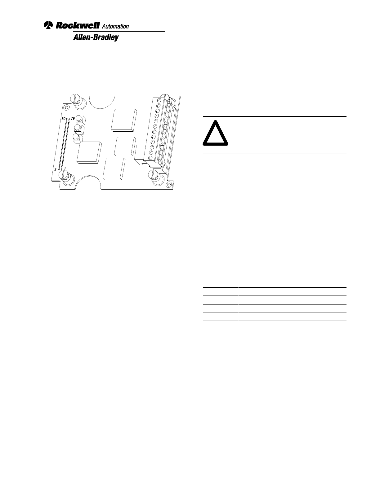
The Cat. No. 1403-NSC Smart Communications Card is
a microprocessor-controlled dual-port communication
plug-in accessory to the Powermonitor II Master Module.
This accessory provides the Powermonitor II with two
active communication ports which can be used at the
same time. Required configuration parameters (R I/O
rack address, baud rates, etc.) are provided by
configuring the Master Module. One port is dedicated to
the Allen-Bradley PLC R I/O network and the other
port is software configurable for either EIA Standards
RS-232C or RS-485. (There are no hardware options to
configure when the card is installed.)
Figure 1. Cat. No 1403-NSC Communications Module
Serial Transmit (TXD) LED
Serial Receive (RXD) LED
Performance Features
The Smart Communication Card performance features
include:
• PLC via R I/O
• SLC 500 via R I/O with (1747-SN) Series B or later
scanner module
• SLC 500 via DF-1 master slave protocol
• R I/O Baud rates: 57.6K baud-230K baud
• Serial Baud rates: 1,200–19,200 baud
• Simultaneous R I/O and serial communication
• 124 units per subnet, 255 per network via RS-485
•
500 V isolation on communications ports
• Fully software configurable, no hardware jumpers
required
Finger hold
Publication
1403-5.1
Captive fastening screw
R I/O Active LED
Connector
Page 3
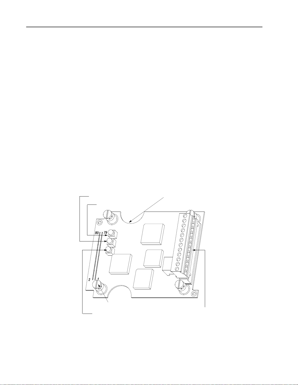
Installation
ATTENTION: Please follow
appropriate ESD procedures before
!
1. T
o remove the blank plate on the Master Module,
unscrew the two corner retaining screws as shown in
Figure 2. Save these two screws for reassembly
Figure 2.
removal and/or installation of the Smart
Communications Card. Failure to follow
these procedures can result in physical
damage to both the Smart
Communications Card and the Master
Module.
Smart Communications Card
ith the Master Module labels right side up, place
5. W
the card into opening on the left side. The card to
Master Module connector should align properly when
the top right and bottom left guide pins of the Master
Module mate with holes in the card. W
thumb, press just above the card to Master Module
connector to attach the connector. Tighten the four
corner screws.
Figure 3.
.
ith your left
3
2. If you plan to remove the communications card at a
later date, retain the blank plate. Otherwise, dispose
of properly.
3. Remove the communications card from the static
protection shipping bag.
4.
Grasp the card with the components side up and the
three LEDs on the left. Place the right index finger in
the top notch and the thumb in the bottom notch.
6. Place the closure plate over the opening and secure it
with the two screws from the original blank plate.
Figure 4.
Note: Refer to Appendix E, Specifications for screw
torque requirements and wire sizes.
Publication
1403-5.1
Page 4
4
RS 485
(
)
4000 ft/19.2kB
3-wire Shielded
1770 CD
10,000 ft /57.6kBaud
R I/O
(Bl
)
5,000 ft/115.2kBaud
Smart Communications Card
Wiring
ATTENTION: Special high level
isolation is required between units when
!
Table A. Wiring Connections
Connector
the possibility of high ground potential
dif
ferences exist. This may occur when
separate grounds are used or when
communicating to a unit connected to a
power ground mat. Failure to do so can
lead to personal injury or death, property
damage, or economic loss.
Communication
Format
RS-485
RS-232
R-I/O
Terminal #
(Counting
from the
bottom up)
12 Do not connect
11 Do not connect
10 SHLD Cable shield grounding point
9 – Minus signal data
8 + Plus signal data
7 RXD
6 TXD PC Receive, DB25, pin3 (DB9, pin 2)
5 SG
4 SHLD Cable Shield
3 1 Blue Wire insulation
2 SHLD Cable shield ground point
1 2 Clear wire insulation
Terminal
Label
Intended Use, Pin Connection,
or Wire Color
PC Transmit, DB25, pin 2,
(DB9, pin 3)
PC signal return, DB25, pin 7
(DB9, pin 5)
Recommended
Cable Type
2-wire shielded
Belden 9841
3-wire Shielded
(Belden 9608)
1770-CD
Twinaxial
ue Hose
(Belden 9463)
Maximum Cable
Length/Baud Rate
4000 ft/19.2kB
50 ft/19.2kB
1
ft 7.kB
5,000 ft/115.2kBaud
2,500 ft/230.4kBaud
Notes:
1. The communications topology for both R I/O and
RS-485 is designed to operate in a daisy-chain
topology. Use of the star or bridging method will
cause signal distortion unless impedances are
matched for each spur. Bridging is not recommended
without matching networks.
2. To prevent end reflections, each end of the daisy-
chain should be terminated in the characteristic
impedance for the cable, the baud rate, and frequency
used.
Communication
RS-485 1200–19.2k
R I/O
Publication
Format
1403-5.1
Baud Rate
57.6–115.2k
230.4k
Terminating
Resistor
150 Ω 1/4 W
150 Ω 1/4 W
84 Ω 1/4 W
3. Each
end section of cable should have the shield
connected to the terminal labeled SHLD. This SHLD
ground provides a high frequency ground, while
limiting DC or power line frequencies from flowing
down the cable shield.
4. The RS-485 receivers in the communications card
provide a 1/4 load impedance instead of the normal
full load impedance. This therefore allows the use of
four times the number of receivers (32 4 or 128
total) on one network.
Page 5
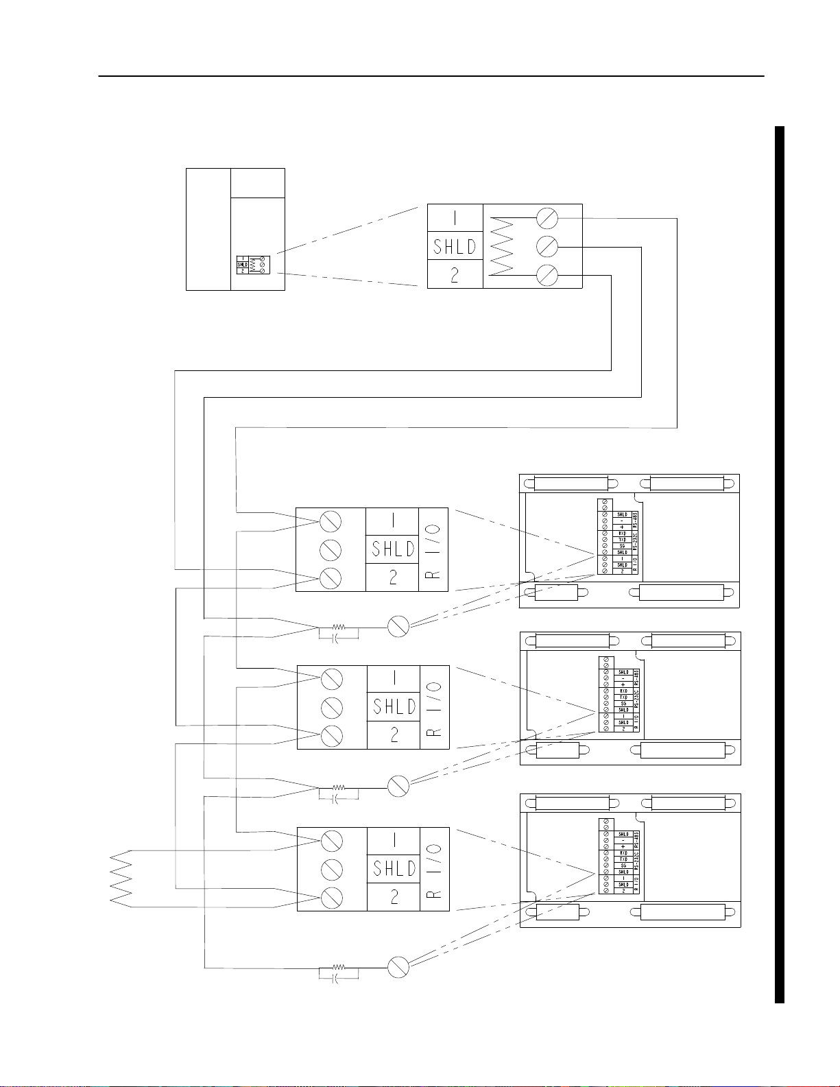
Figure 5. R I/O Wiring
PLC PROCESSOR
INTERNAL TERMINATING
150Ω
RESISTOR
Smart Communications Card
BLUE
SHIELD
CLEAR
5
150KΩ
0.047uF
150KΩ
0.047uF
Powermonitor
DEVICE #1
Powermonitor
DEVICE #2
Powermonitor
DEVICE #3
II
II
II
84Ω OR
150
Ω RESISTOR
150KΩ
0.047uF
Note: All
possible between the R/C and the cover plate.
ground wires should be kept as short as
Publication
1403-5.1
Page 6
6
Smart Communications Card
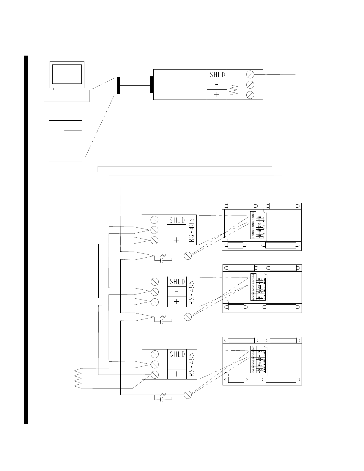
Figure 6. RS-485 Wiring
IBM PC
PLC PROCESSOR
RS–232C
EXTERNAL
RS–232C
TO RS–485
CONVERTER
150Ω
RESISTOR
150Ω RESISTOR
150KΩ
0.047uF
150KΩ
0.047uF
150KΩ
0.047uF
Note: All
possible between the R/C and the cover plate.
Powermonitor
DEVICE #1
Powermonitor II
DEVICE #2
Powermonitor II
DEVICE #3
II
ground wires should be kept as short as
Publication
1403-5.1
Page 7
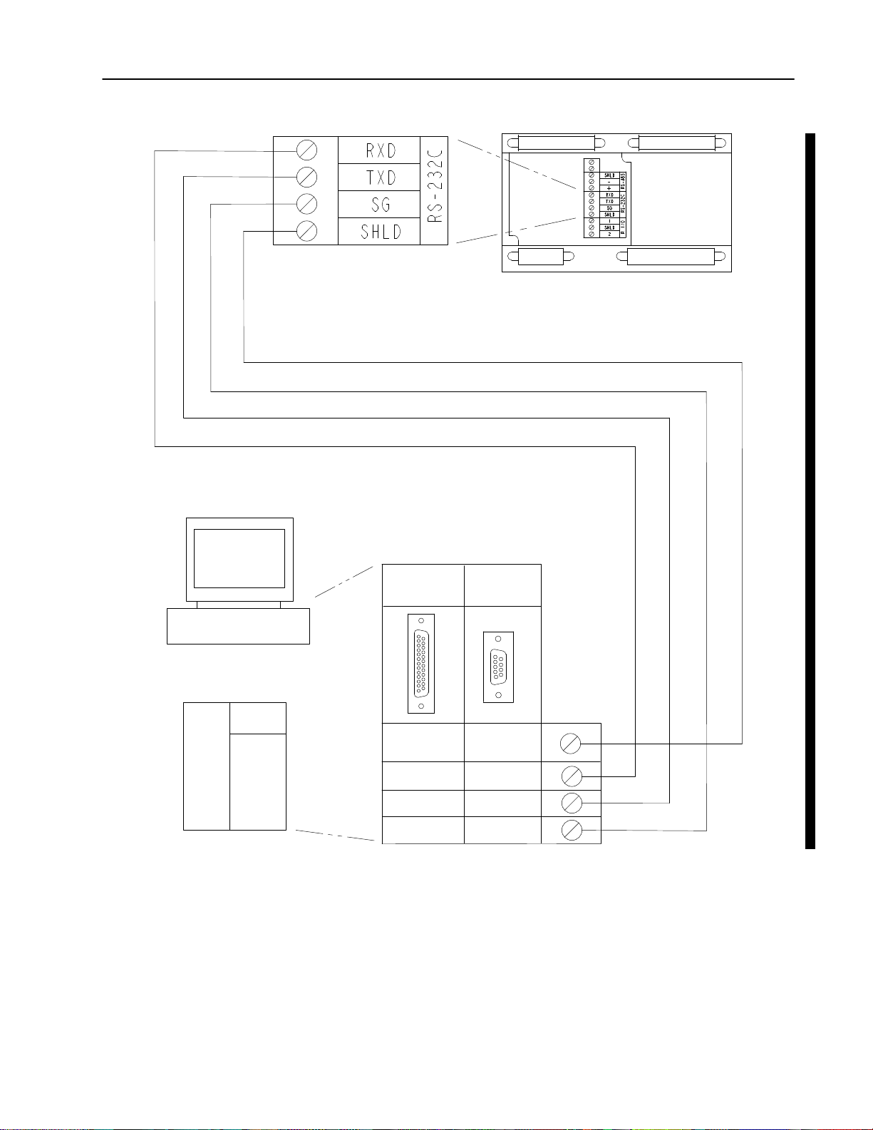
Figure 7. RS-232C Wiring
Smart Communications Card
Powermonitor II
7
IBM PC
PLC PROCESSOR
Note: For
be connected directly to the chassis ground terminal
located on the communication card cover plate. The
exposed shield wire should be as short as possible.
CE compliance, the communication cable shield must
25 PIN
D–SHELL
9 PIN
D–SHELL
Field Service Considerations
If the Smart Communications Card requires service,
please contact your nearest Allen-Bradley Sales Of
To minimize your inconvenience, the initial installation
should be performed in a manner which makes
removal easy
.
fice.
1
7
CASE
GROUND
2
3
3
2
5
Publication
1403-5.1
Page 8

8
Smart Communications Card
General Operation
Communications Card Set-Up
All
communications card options such as
communications format, baud rate, address, etc., are set
by configuring the Master Module. Refer to
Powermonitor II Instruction Sheet
Chapter 4.
Table B. LED Indicators
LED
Location
Top Red RS-232 or RS-485 Receive
Middle Red RS-232 or RS-485 Transmit
Bottom Green
Configuration
Items
Communication
, Publication 1403-5.0,
LED
Color
Port Assignment LED State and Communications Condition
R I/O
Indicators
Figure 1. on page 2 shows the location of the LED
Indicators on the communications card.
OFF = Idle
ON/OFF Pulsing = Receiving Data
OFF = Idle
ON/OFF Pulsing = Transmitting Data
ON = Communications Established
ON/OFF Blinking = Communications Established With Some Errors
OFF = Communications Not Established
Table C. Communication Configuration Items
Parameter
R I/O Rack Address
R I/O Group Number Determines the group number of the logical rack.
R I/O Last Rack
R I/O Baud Rate Specifies the baud rate of the RIO network.
Serial Delay
Serial Mode Specifies the serial communications mode.
RS-232/RS-485 Baud
Rate
Serial Device Identifier
Specifies the logical rack of the Smart Communication
Card.
Defines whether or not the configured rack is the last
rack.
Defines the delay in ms between the request and
response serial packets.
Determines the baud rate for the serial communications.
Defines the specific serial address. A value of 255 is
used as a broadcast address.
Description Range Default
0 to 63 1
0 = First Quarter
2 = Second Quarter
4 = Third Quarter
6 = Fourth Quarter
0 = No
1 = Yes
0 to 56K
1 to 115K
2 to 230K
0 to 15 0
0 = RS-485
1 = RS-232
0 to 1200
1 to 2400
2 to 4800
3 to 9600
4 to 19200
0 to 254 Device ID#
0 = First
Quarter
0 = No
0 to 56K
1 = RS-232
3 to 9600
User
Setting
Publication
1403-5.1
Page 9
Catalog Number Explanation
Communications Cards
Appendix A
1403
Bulletin Number Type of Device
Power Quality and
1403 = Plug-in Communications Card for Bulletin 1403-MM Devices
Automation Products
- NSC
NSC =
(RS-232C / RS-485 / Allen-Bradley R I/O Protocols)
Publication
1403-5.1
Page 10

A–2 Catalog Number Explanation
Publication
1403-5.1
Page 11

Appendix B
Block Transfer Read/
Smart Communication Card Data Tables
Table B.1 Data Table List
Table Name
Device Configuration Data Table 32 44
Smart Communication Card Data Table 21 30
Command Data Table 12 22 Block Transfer Write B–5
Bit Fields for Command Data Table
(Command Word 1)
Bit Fields for Command Data Table
(Command Word 2)
Voltage/Current Data 23 53 Block Transfer Read B–6
Real Time Power Data 25 62 Block Transfer Read B–7
Cumulative Power Data 7 45 Block Transfer Read B–9
Demand Data 18 42 Block Transfer Read B–10
Event Log 12 23 Block Transfer Read B–11
Voltage/Current/Miscellaneous Snapshot Log
Data Table
Power Snapshot Log Data Table 30 59 Block Transfer Read B–13
Min_Max Log 8 24 Block Transfer Read B–15
Log Selection Command Table 4 9 Block Transfer Write B–16
Available Min/Max Log Parameters 84 — — B–17
Even Harmonic Distortion Table 29 60 Block Transfer Read B–18
Odd Harmonic Distortion Table 29 61 Block Transfer Read B–19
Even Harmonic Magnitude Data Table 29 58 Block Transfer Read B–21
Odd Harmonic Magnitude Data Table 29 57 Block Transfer Read B–22
Even Harmonic Phase Angle Data Table 29 56 Block Transfer Read B–24
Odd Harmonic Phase Angle Data Table 29 55 Block Transfer Read B–25
Oscillogram Capture Data 54 63 Block Transfer Read B–27
Diagnostic Data Table (Self-test Results) 35 39 Block Transfer Read B–29
Setpoint Setup Data Table 9 20
Setpoint Type — — — B–31
Setpoint Action — — — B–31
Relay/Setpoint Status Table 29 38 Block Transfer Read B–32
Status Inputs Bitfield Definitions 16 bits — — B–33
Alarm Word Bitfield Definitions 16 bits — — B–33
Setpoint Status Bitfield Definitions 16 bits — — B–33
Number of
Parameters
— — — B–6
— — — B–6
28 54 Block Transfer Read B–12
ID/Number
of Words
Type of Table Page
Block Transfer Read/
Write
Block Transfer Read/
Write
Block Transfer Read/
Write
B–2
B–4
–
B–30
Publication
1403-5.1
Page 12
B–2 Smart Communication Card Data Tables
БББББББББ
БББББББББ
Á
Á
Á
БББББББББ
Á
Á
Á
БББББББББ
Á
Á
Á
Á
Á
Á
Á
Á
Á
Á
Á
БББББББББ
Á
Á
Á
БББББББББ
БББББББББ
БББББББББ
БББББББББ
БББББББББ
БББББББББ
БББББББББ
БББББББББ
БББББББББ
БББББББББ
БББББББББ
БББББББББ
БББББББББ
БББББББББ
БББББББББ
БББББББББ
БББББББББ
БББББББББ
БББББББББ
БББББББББ
БББББББББ
БББББББББ
БББББББББ
БББББББББ
БББББББББ
БББББББББ
БББББББББ
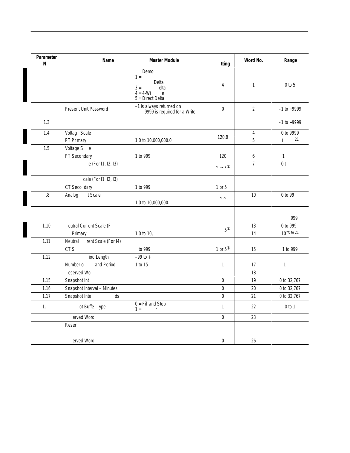
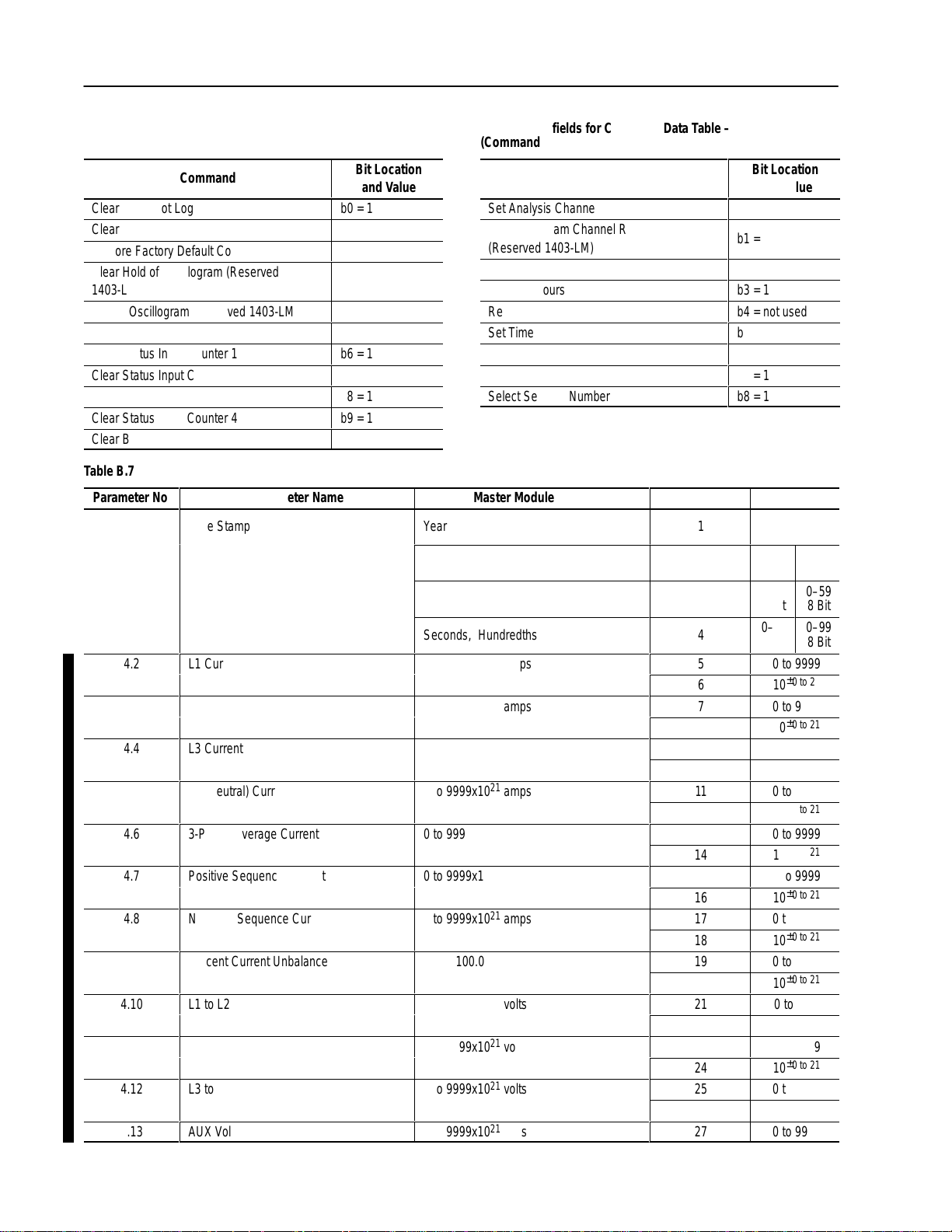
Table B.2 Device Configuration Data Table – Write and Read
Parameter
No.
ÁÁÁ
1.1
ÁÁÁ
ÁÁÁ
1.2
ÁÁÁ
1.3
1.4
1.5
1.6
1.7
1.8
1.9
1.10
1.11
1.12
1.13
1.14
1.15
1.16
1.17
1.18
Parameter Name
ББББББББ
Voltage Mode
ББББББББ
ББББББББ
Present Unit Password
ББББББББ
New Password
Voltage Scale
PT Primary
Voltage Scale
PT Secondary
Current Scale (For I1, I2, I3)
CT Primary
Current Scale (For I1, I2, I3)
CT Secondary
Analog Input Scale
PT Primary
Analog Input Scale
PT Secondary
Neutral Current Scale (For I4)
CT Primary
Neutral Current Scale (For I4)
CT Secondary
Demand Period Length
Number of Demand Periods
Reserved Word
Snapshot Interval – Hours
Snapshot Interval – Minutes
Snapshot Interval – Seconds
Snapshot Buffer Type
Reserved Word
Reserved Word
Reserved Word
Reserved Word
Master Module Range
0 = Demo
1 = Single
ББББББББ
2 = Open Delta
ББББББББ
3 = 3-Wire Delta
4 = 4-Wire Wye
ББББББББ
5 = Direct Delta
–1 is always returned on a Read
0 to 9999 is required for a Write
ББББББББ
–1 does not change the password
0 to 9999 is new password value
1.0 to 10,000,000.0
1 to 999
1.0 to 10,000,000.0
1 to 999
1.0 to 10,000,000.0
1 to 999
1.0 to 10,000,000.0
1 to 999
–99 to +99
1 to 15
0 = Fill and Stop
1 = Circular
Default
Setting
ÁÁ
4
ÁÁ
ÁÁ
0
ÁÁ
0
120.0
120
1 or 5
1 or 5
1.0
1
1 or 5
1 or 5
1
1
0
0
0
0
1
0
0
0
0
Word No.
ÁÁÁÁ
1
ÁÁÁÁ
ÁÁÁÁ
ÁÁÁÁ2ÁÁÁÁ
3
4
5
6
➀
➀
7
8
➀
9
10
11
12
➀
➀
13
14
➀
15
16
ÁÁÁÁ
ÁÁÁÁ
ÁÁÁÁ
–1 to +9999
–1 to +9999
0 to 9999
10
1 to 999
0 to 9999
10
1 to 999
0 to 9999
10
1 to 999
0 to 9999
10
1 to 999
–99 to +99
17
18
19
20
21
0 to 32,767
0 to 32,767
0 to 32,767
22
23
24
25
26
Range
0 to 5
±
0 to 21
±
0 to 21
±
0 to 21
±
0 to 21
1 to 15
0 to 1
Publication
1403-5.1
Page 13
B–3Smart Communication Card Data Tables
Á
Á
Á
Á
Á
Á
Á
Á
Á
Á
Á
Á
Á
Á
Á
Á
Á
Á
Á
Á
Á
Á
Á
Á
Á
Á
Á
Á
Á
Á
Á
Á
Á
Á
Á
Á
Á
Á
Á
Á
Á
Á
Á
Á
Á
Á
Á
Á
Á
Á
Á
Á
Á
Á
Á
Á
Á
Á
Á
Á
Á
Á
Á
Á
Á
Á
Á
Á
Á
Á
Á
Á
Á
Á
Á
Á
Á
Á
0
Á
Á
Á
Á
Á
0
Á
Á
Á
Á
Á
Á
Á
Á
Á
Á
Á
Á
Parameter
No.
1.19
ÁÁÁ
ÁÁÁ
1.20
ÁÁÁ
1.21
1.22
ÁÁÁ
ÁÁÁ
1.23
ÁÁÁ
ÁÁÁ
ÁÁÁ
ÁÁÁ
1.24
ÁÁÁ
ÁÁÁ
ÁÁÁ
1.25
1.26
ÁÁÁ
1.27
1.28
ÁÁÁ
1.29
ÁÁÁ
1.30
1.31
1.32
ÁÁÁ
1.33
Parameter Name
Reserved Word
Output Pulse Relay No.
БББББББ
БББББББ
Output Pulse Parameter
БББББББ
Output Pulse Increment
Output Pulse Width (ms)
БББББББ
БББББББ
Ch A 12 Cycle Oscillogram
БББББББ
БББББББ
БББББББ
БББББББ
Ch B 12 Cycle Oscillogram
БББББББ
БББББББ
БББББББ
Oscillography Type
Number of Pretrigger Cycles for
the 12 Cycle Oscillogram
БББББББ
IEEE 519 Max. Short Circuit
Current
IEEE 519 Max. Demand/Load
Current
БББББББ
Save Status Changes to Event
БББББББ
Log
Vaux Voltage Mode
Enable THD
Enable Min_Max Log
БББББББ
Data Format
Master Module Range
0 = None
1 = Relay 1
ББББББББ
2 = Relay 2
0 = kWh Forward
ББББББББ
1 = kWh Reverse
2 = kVarh Forward
ББББББББ
3 = kVarh Reverse
1 to 32766
40 to 2000
1 = Phase 1 Voltage
2 = Phase 1 Current
ББББББББ
3 = Phase 2 Voltage
ББББББББ
4 = Phase 2 Current
5 = Phase 3 Voltage
ББББББББ
6 = Phase 3 Current
ББББББББ
7 = Phase 4 Current
1 = Phase 1 Voltage
ББББББББ
2 = Phase 1 Current
3 = Phase 2 Voltage
ББББББББ
4 = Phase 2 Current
ББББББББ
5 = Phase 3 Voltage
ББББББББ
6 = Phase 3 Current
7 = Phase 4 Current
ББББББББ
0 = Hold
1 = Overwrite
–1 = No Pretrig
0 to +8 = Cycles
ББББББББ
0.0 to 10,000,000.0
ББББББББÁÁ
0.0 to 10,000,000.0
0 = No
ББББББББ
1 = Yes
0 = AC
1 = DC
0 or 1
0 = No
ББББББББ
1 = Yes
0 = Integer/Exponent
1 = Floating Point
Default
Setting
0
0
Á
Á
0
Á
1
100
Á
Á
1
Á
Á
Á
Á
2
Á
Á
Á
1
0
Á
0
0
0
Á
0
1
1
Á
0
Word No.
27
28
ÁÁÁÁ
ÁÁÁÁ
29
ÁÁÁÁ
30
31
ÁÁÁÁ
ÁÁÁÁ
32
ÁÁÁÁ
ÁÁÁÁ
ÁÁÁÁ
ÁÁÁÁ
33
ÁÁÁÁ
ÁÁÁÁ
ÁÁÁÁ
34
35
ÁÁÁÁ
36
37
38
ÁÁÁÁ
39
40
ÁÁÁÁ
41
42
43
ÁÁÁÁ
44
Range
0 to 2
ÁÁÁ
ÁÁÁ
0 to 3
ÁÁÁ
1 to 32766
40 to 2000
ÁÁÁ
ÁÁÁ
1 to 7
ÁÁÁ
ÁÁÁ
ÁÁÁ
ÁÁÁ
1 to 7
ÁÁÁ
ÁÁÁ
ÁÁÁ
0 to 1
–1 to +8
ÁÁÁ
0 to 9999
±
0 to 21
10
0 to 9999
ÁÁÁ
±
0 to 21
10
0 to 1
ÁÁÁ
0 to 1
0 to 1
0 to 1
ÁÁÁ
0 to 1
➀
This
value will be 1 for 1 Amp Master Module (Cat. No. 1403-MM01X) or 5 for a 5 Amp Master Module (Cat. No. 1403-MM05X).
Publication
1403-5.1
Page 14
B–4 Smart Communication Card Data Tables
Á
Á
Á
Á
Á
Á
Á
Á
Á
Á
Á
Á
Á
Á
Á
Á
Á
Á
Á
Á
Á
Á
Á
Á
Á
Á
Á
Á
Á
Á
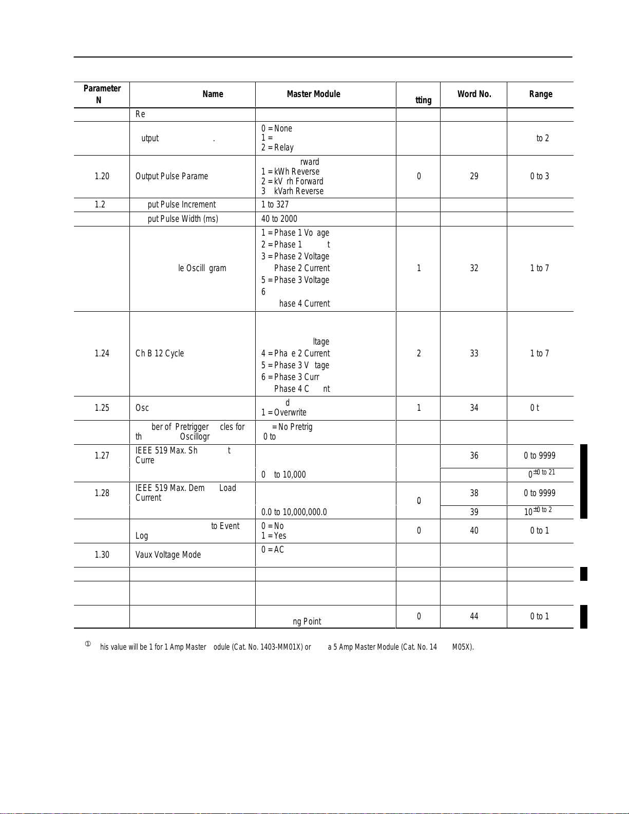
Table B.3 Smart Communication Card Data Table – Write and Read
Note: The device will not respond to a broadcast of this table.
Parameter
No.
2.1
2.2
2.3
ÁÁÁ
2.4
ÁÁÁ
2.5
2.6
ÁÁÁ
2.7
ÁÁÁ
ÁÁÁ
2.8
2.9
ÁÁÁ
2.10
2.11
2.12
2.13
2.14
2.15
2.16
2.17
2.18
2.19
2.20
2.21
ÁÁÁ
Parameter Name
R I/O Rack Address
R I/O Group Number
R I/O Last Rack
ББББББББББ
R I/O Baud Rate
ББББББББББ
Serial Response Delay
Serial Type Specifier RS-232 or RS-485
ББББББББББ
SCC RS-232/RS-485 Baud Rate
ББББББББББ
ББББББББББ
Serial Device Identifier
R I/O Port Data Format
ББББББББББ
Serial Port Data Format
Reserved
Reserved
Reserved
Reserved
Reserved
Reserved
Reserved
Reserved
Reserved
Reserved
Present Unit Password
ББББББББББ
Reserved
Reserved
Reserved
Reserved
Reserved
Reserved
Reserved
Reserved
Reserved
Master Module Range
0 to 63
0 to 6
0 = No – Default
1 = Yes
БББББББББ
0 = 56K – Default
1 = 115K
2 = 230K
БББББББББ
0 to 15
0 = RS-485
1 = RS-232 – Default
0 = 1200
1 = 2400
БББББББББ
2 = 4800
БББББББББ
3 = 9600 – Default
4 = 19200
БББББББББ
0 to 255
0 = Integer/Exponent
БББББББББ
1 = Floating Point
0 = Integer/Exponent
1 = Floating Point
–1 is always returned for a Read
БББББББББ
0 to 9999 is required for a Write
PLC Word No.
1
2
3
ÁÁÁ
4
ÁÁÁ
5
6
ÁÁÁ
7
ÁÁÁ
ÁÁÁ
8
9
ÁÁÁ
10
11
12
13
14
15
16
17
18
19
20
21
ÁÁÁ
22
23
24
25
26
27
28
29
30
Range
0 to 63
0 to 6
0 to 1
ÁÁÁ
0 to 2
ÁÁÁ
0 to 15
0 to 1
ÁÁÁ
0 to 4
ÁÁÁ
ÁÁÁ
0 to 255
0 to 1
ÁÁÁ
0 to 1
–1 to +9999
ÁÁÁ
Publication
1403-5.1
Page 15
Table B.4 Command Data Table Write
Á
Á
Á
Á
Á
Á
Á
Á
Á
Á
Á
Á
Á
Á
Á
Á
Á
Á
Á
Á
Á
Á
Á
Á
Á
Á
Á
Á
Á
Á
Á
Á
Á
Á
Á
Á
Á
Á
Á
Á
Á
Á
Á
Á
Á
Á
Á
Á
Á
Á
Á
Á
Á
Á
Á
Á
Á
Á
Á
Á
Á
Á
Á
Á
Á
Á
Á
Á
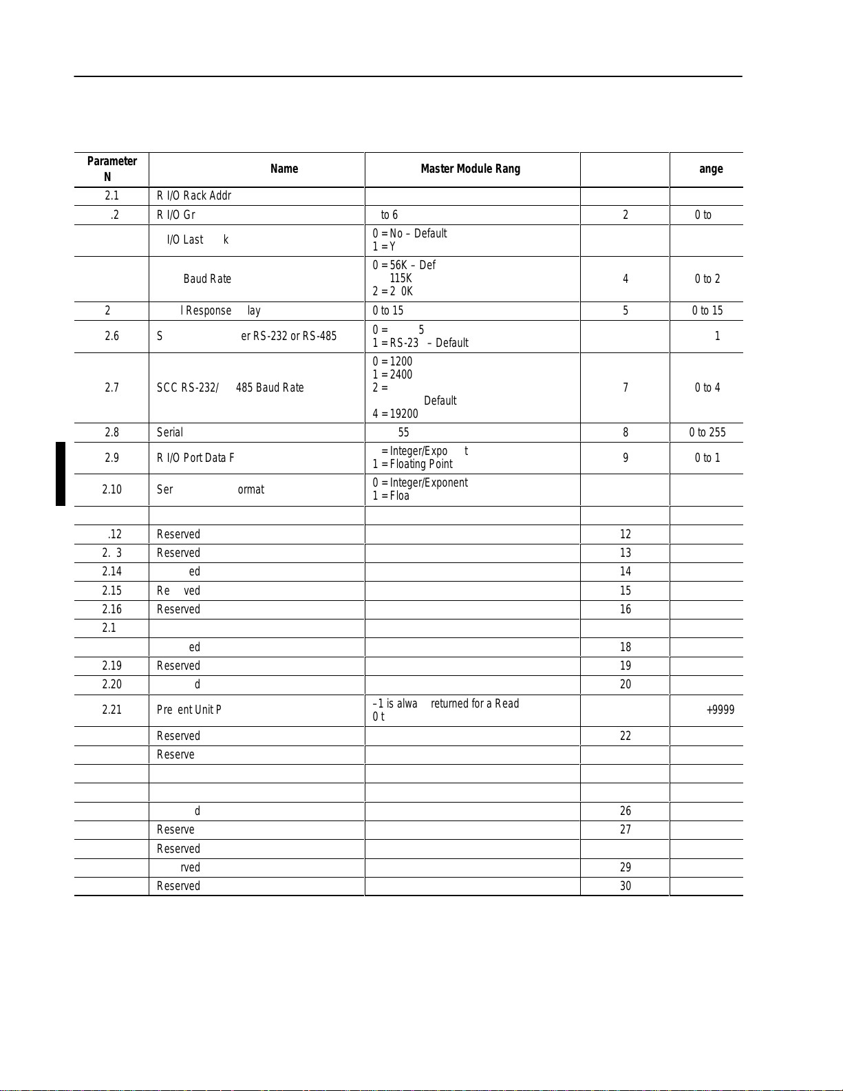
B–5Smart Communication Card Data Tables
Parameter No.
3.1
3.2
Command Word 1 (Bit Fields)
Command Word 2 (Bit Fields)
Parameter Name
Master Module Range
0 to 2047
0 to 511
1 = L1 Voltage
ÁÁÁ
ÁÁÁ
3.3
ÁÁÁ
ÁÁÁ
БББББББББ
БББББББББ
Harmonic Analysis
БББББББББ
БББББББББ
➀
БББББББББ
2 = L1 Current
3 = L2 Voltage
БББББББББ
4 = L2 Current
5 = L3 Voltage
БББББББББ
6 = L3 Current
БББББББББ
7 = L4 Current
1 = L1 Voltage
ÁÁÁ
ÁÁÁ
3.4
ÁÁÁ
ÁÁÁ
ÁÁÁ
3.5
3.6
3.7
3.8
ÁÁÁ
ÁÁÁÁБББББББББÁБББББББББ
БББББББББ
БББББББББ
Oscillogram Channel Request
(Reserved 1403-LM)
БББББББББ
БББББББББ
БББББББББ
W Hour Data for Set Command
➀
➀
VAR Hour Data for Set Command➀–9999x108 to +9999x10
Reserved
Time for Set Command
БББББББББ
➀
2 = L1 Current
БББББББББ
3 = L2 Voltage
4 = L2 Current
БББББББББ
5 = L3 Voltage
БББББББББ
6 = L3 Current
7 = L4 Current
БББББББББ
8 = Ch–A 12 Cycle
9 = Ch–B 12 Cycle
БББББББББ
–9999x108 to +9999x10
8
8
Year
БББББББББ
Month, Day
Hour, Minutes
ÁÁÁ
ÁÁÁÁБББББББББÁБББББББББ
3.9
ÁÁÁ
3.10
ÁÁÁ
3.11
3.12
БББББББББ
Force Specifics Relay 1
БББББББББ
Force Specifics Relay 2
БББББББББ
Setpoint Number
➀
➀
➀
Present Unit Password
БББББББББ
Seconds, Hundredths
1 = Energize
2 = De-energize
БББББББББ
4 = Remove Force
1 = Energize
2 = De-energize
БББББББББ
4 = Remove Force
1 to 20
0 to 9999
Reserved
Reserved
Reserved
3.13
ÁÁÁ
➀
See T
able B.5 in Publication 1403-5.1 for specific command bits to
enable these features.
Data Format
БББББББББ
0 = Integer/Exponent
1 = Floating Point
БББББББББ
Word No.
1
2
ÁÁÁ
ÁÁÁ
3
ÁÁÁ
ÁÁÁ
ÁÁÁ
ÁÁÁ
4
ÁÁÁ
ÁÁÁ
ÁÁÁ
5
6
7
8
9
10
Range
0 to 2047
0 to 511
ÁÁÁ
ÁÁÁ
1 to 7
ÁÁÁ
ÁÁÁ
ÁÁÁ
ÁÁÁ
1 to 9
ÁÁÁ
ÁÁÁ
ÁÁÁ
–9999 to 9999
±
0 to 21
10
–9999 to 9999
±
0 to 21
10
9
10
0–99
ÁÁÁ11ÁÁÁ
12
ÁÁÁ
ÁÁÁ13Á
14
ÁÁÁ
15
ÁÁÁ
16
ÁÁÁ
17
18
16 Bit Integer
1–12
1–31
Á
Á
ÁÁÁ
ÁÁÁ
8 Bit
0–23
8 Bit
0–59
8 Bit
1, 2, 4
1, 2, 4
Á
8 Bit
0–59
8 Bit
Á
0–99
Á
8 Bit
1 to 20
0 to 9999
19
20
21
22
ÁÁÁ
0 to 1
ÁÁÁ
Publication
1403-5.1
Page 16
B–6 Smart Communication Card Data Tables
Á
Á
Á
Á
Á
Á
Á
Á
Á
Á
Á
Á
Á
Á
Table B.5 Bit Fields for Command Data Table –
(Command Word 1)
БББББББББ
Command
Clear Snapshot Log
Clear Min_Max Log
Restore Factory Default Configuration
Clear Hold of Oscillogram (Reserved
БББББББББ
1403-LM)
Initiate Oscillogram (Reserved 1403-LM)
Force Self Test
Clear Status Input Counter 1
Clear Status Input Counter 2
Clear Status Input Counter 3
Clear Status Input Counter 4
БББББББББ
Clear Battery Usage Timer
Bit Location
ÁÁÁÁ
and Value
b0 = 1
b1 = 1
b2 = 1
b3 = 1
ÁÁÁÁ
b4 = 1
b5 = 1
b6 = 1
b7 = 1
b8 = 1
b9 = 1
ÁÁÁÁ
b10 = 1
Table B.6 Bit fields for Command Data Table –
(Command Word 2)
БББББББББ
Command
Set Analysis Channel Request
Set Oscillogram Channel Request
(Reserved 1403-LM)
Set W Hours
Set VAR Hours
Reserved
Set Time
Relay 1
Relay 2
Select Setpoint Number
Table B.7 Voltage/Current Data – Read
Parameter No.
4.1
ÁÁÁÁБББББББББÁБББББББББ
Time Stamp
Parameter Name
Master Module Range
Year
Month, Date
Hour, Minute
ÁÁÁÁБББББББББÁБББББББББ
4.2
4.3
L1 Current
L2 Current
Seconds, Hundredths
0 to 9999x1021 amps
0 to 9999x1021 amps
4.4
4.5
4.6
4.7
4.8
ÁÁÁ
L3 Current
L4 (Neutral) Current
3-Phase Average Current
Positive Sequence Current
Negative Sequence Current
БББББББББ
0 to 9999x1021 amps
0 to 9999x1021 amps
0 to 9999x1021 amps
0 to 9999x1021 amps
0 to 9999x1021 amps
БББББББББ
4.9
4.10
4.11
4.12
ÁÁÁ
4.13
Percent Current Unbalance
L1 to L2 Voltage
L2 to L3 Voltage
L3 to L1 Voltage
БББББББББ
AUX Voltage
0.0 to 100.0
0 to 9999x1021 volts
0 to 9999x1021 volts
0 to 9999x1021 volts
БББББББББ
0 to 9999x1021 volts
Bit Location
ÁÁÁÁ
and Value
b0 = 1
b1 = 1
b2 = 1
b3 = 1
b4 = not used
b5 = 1
b6 = 1
b7 = 1
b8 = 1
Word No.
1
2
ÁÁÁ
3
4
ÁÁÁ
5
6
7
8
9
10
11
12
13
14
15
16
ÁÁÁ17ÁÁÁ
18
19
20
21
22
23
24
25
ÁÁÁ26ÁÁÁ
27
Range
0–99
16 Bit Integer
1–12
1–31
Á
8 Bit
0–23
8 Bit
0–59
Á
8 Bit
Á
8 Bit
0–59
8 Bit
0–99
Á
8 Bit
0 to 9999
±
0 to 21
10
0 to 9999
±
0 to 21
10
0 to 9999
±
0 to 21
10
0 to 9999
±
0 to 21
10
0 to 9999
±
0 to 21
10
0 to 9999
±
0 to 21
10
0 to 9999
±
0 to 21
10
0 to 9999
±
0 to 21
10
0 to9999
±
0 to 21
10
0 to 9999
±
0 to 21
10
0 to 9999
±
0 to 21
10
0 to 9999
Publication
1403-5.1
Page 17
B–7Smart Communication Card Data Tables
Á
Á
Á
Á
Á
Á
Á
Á
Á
Á
Á
Á
Á
Á
Á
Á
Á
Á
Á
Á
Á
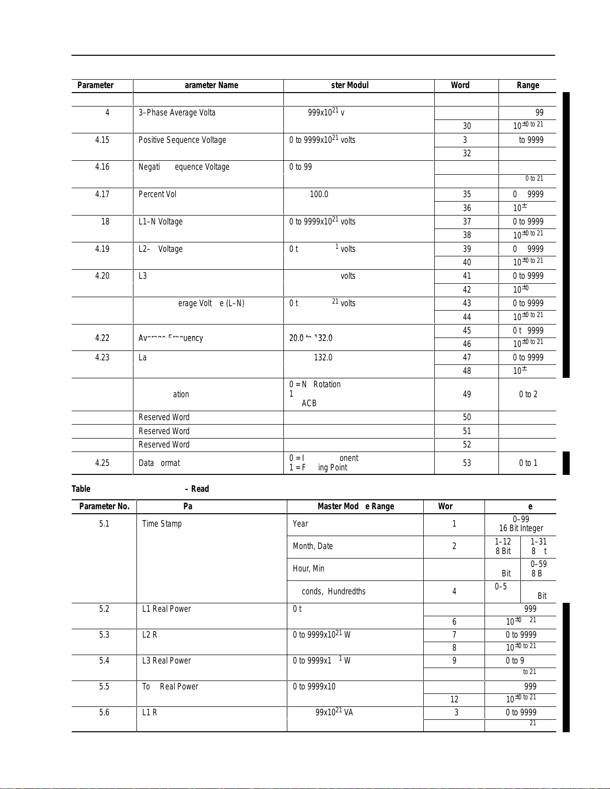
Parameter No.
4.14
4.15
4.16
4.17
4.18
ÁÁÁ
4.19
4.20
4.21
4.22
4.23
4.24
ÁÁÁ
4.25
ÁÁÁ
Parameter Name
3–Phase Average Voltage (L–L)
Positive Sequence Voltage
Negative Sequence Voltage
Percent Voltage Unbalance
L1–N Voltage
БББББББББ
L2–N Voltage
L3–N Voltage
3–Phase Average Voltage (L–N)
Average Frequency
Last Cycle Frequency
Phase Rotation
БББББББББ
Reserved Word
Reserved Word
Reserved Word
Data Format
БББББББББ
Master Module Range
0 to 9999x1021 volts
0 to 9999x1021 volts
0 to 9999x1021 volts
0.0 to 100.0
0 to 9999x1021 volts
БББББББББ
0 to 9999x1021 volts
0 to 9999x1021 volts
0 to 9999x1021 volts
20.0 to 132.0
20.0 to 132.0
0 = No Rotation
1 = ABC
БББББББББ
2 = ACB
0 = Integer/Exponent
1 = Floating Point
БББББББББ
Word No.
28
29
30
31
32
33
34
35
36
ÁÁÁ37ÁÁÁ
38
39
40
41
42
43
44
45
46
47
48
49
ÁÁÁ
Range
±
0 to 21
10
0 to 9999
±
0 to 21
10
0 to 9999
±
0 to 21
10
0 to 9999
±
0 to 21
10
0 to 9999
±
0 to 21
10
0 to 9999
±
0 to 21
10
0 to 9999
±
0 to 21
10
0 to 9999
±
0 to 21
10
0 to 9999
±
0 to 21
10
0 to 9999
±
0 to 21
10
0 to 9999
±
0 to 21
10
0 to 2
ÁÁÁ
50
51
52
53
ÁÁÁ
0 to 1
ÁÁÁ
Table B.8 Real Time Power Data – Read
Parameter No.
5.1
ÁÁÁ
ÁÁÁÁБББББББББÁББББББББ
Time Stamp
БББББББББ
Parameter Name
Master Module Range
Year
ББББББББ
Month, Date
Hour, Minute
ÁÁÁ
ÁÁÁÁБББББББББÁББББББББ
5.2
БББББББББ
L1 Real Power
ББББББББ
Seconds, Hundredths
0 to 9999x1021 W
5.3
5.4
5.5
5.6
L2 Real Power
L3 Real Power
Total Real Power
L1 Reactive Power
0 to 9999x1021 W
0 to 9999x1021 W
0 to 9999x1021 W
0 to 9999x1021 VAR
Word No.
1
ÁÁÁ
2
ÁÁÁ
Range
16 Bit Integer
ÁÁÁÁ
1–12
ÁÁ
8 Bit
0–23
ÁÁÁ3ÁÁ
4
ÁÁÁ
5
6
7
8
9
10
11
12
13
14
8 Bit
0–59
ÁÁ
8 Bit
0 to 9999
10
0 to 9999
10
0 to 9999
10
0 to 9999
10
0 to 9999
10
Publication
0–99
1–31
ÁÁ
8 Bit
0–59
8 Bit
ÁÁ
0–99
ÁÁ
8 Bit
±
0 to 21
±
0 to 21
±
0 to 21
±
0 to 21
±
0 to 21
1403-5.1
Page 18
B–8 Smart Communication Card Data Tables
Á
Á
Á
Á
Á
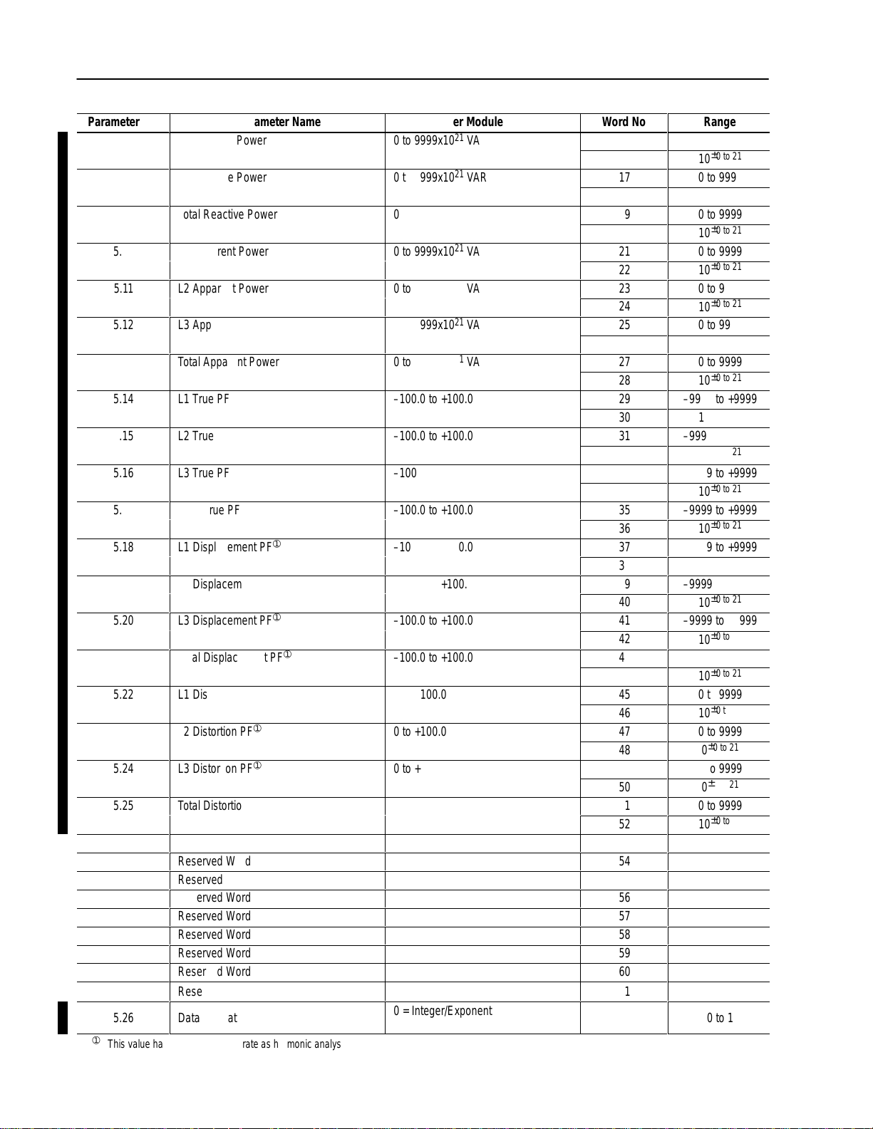
Parameter No.
5.7
5.8
5.9
5.10
5.11
5.12
5.13
5.14
5.15
5.16
5.17
5.18
5.19
5.20
5.21
5.22
5.23
5.24
5.25
L2 Reactive Power
L3 Reactive Power
Total Reactive Power
L1 Apparent Power
L2 Apparent Power
L3 Apparent Power
Total Apparent Power
L1 True PF
L2 True PF
L3 True PF
Total True PF
L1 Displacement PF
L2 Displacement PF
L3 Displacement PF
Total Displacement PF
L1 Distortion PF
L2 Distortion PF
L3 Distortion PF
Total Distortion PF
Parameter Name
➀
➀
➀
➀
➀
➀
➀
➀
Reserved Word
Reserved Word
Reserved Word
Reserved Word
Reserved Word
Reserved Word
Reserved Word
Reserved Word
Reserved Word
5.26
ÁÁÁ
➀
This
value has the same update rate as harmonic analysis.
Data Format
БББББББББ
Master Module Range
0 to 9999x1021 VAR
0 to 9999x1021 VAR
0 to 9999x1021 VAR
0 to 9999x1021 VA
0 to 9999x1021 VA
0 to 9999x1021 VA
0 to 9999x1021 VA
–100.0 to +100.0
–100.0 to +100.0
–100.0 to +100.0
–100.0 to +100.0
–100.0 to +100.0
–100.0 to +100.0
–100.0 to +100.0
–100.0 to +100.0
0 to +100.0
0 to +100.0
0 to +100.0
0 to +100.0
0 = Integer/Exponent
ББББББББ
1 = Floating Point
Word No.
15
16
17
18
19
20
21
22
23
24
25
26
27
28
29
30
31
32
33
34
35
36
37
38
39
40
41
42
43
44
45
46
47
48
49
50
51
52
53
54
55
56
57
58
59
60
61
62
ÁÁÁ
Range
0 to 9999
±
0 to 21
10
0 to 9999
±
0 to 21
10
0 to 9999
±
0 to 21
10
0 to 9999
±
0 to 21
10
0 to 9999
±
0 to 21
10
0 to 9999
±
0 to 21
10
0 to 9999
±
0 to 21
10
–9999 to +9999
±
0 to 21
10
–9999 to +9999
±
0 to 21
10
–9999 to +9999
±
0 to 21
10
–9999 to +9999
±
0 to 21
10
–9999 to +9999
±
0 to 21
10
–9999 to +9999
±
0 to 21
10
–9999 to +9999
±
0 to 21
10
–9999 to +9999
±
0 to 21
10
0 to 9999
±
0 to 21
10
0 to 9999
±
0 to 21
0
0 to 9999
±
0 to 21
0
0 to 9999
±
0 to 21
10
0 to 1
ÁÁÁÁ
Publication
1403-5.1
Page 19
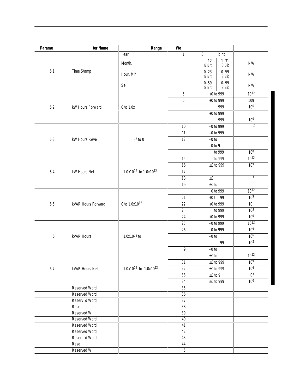
Table B.9 Cumulative Power Data – Read
Á
Á
Á
Á
Á
Á
Á
Á
6.2
kW Hours Forward
0 to 1.0x10
6.3
kW Hours Reverse
1.0x10 to 0
6.4
kW Hours Net
1.0x10 to 1.0x10
6.5
kVAR Hours Forward
0 to 1.0x10
6.6
kVAR Hours Reverse
1.0x10 to 0
6.7
kVAR Hours Net
1.0x10 to 1.0x10
B–9Smart Communication Card Data Tables
Parameter No.
Parameter Name
Master Module Range
Year
ÁÁÁÁÁББББББÁББББББ
6.1
ÁÁÁÁÁББББББÁББББББ
6.2
6.3
6.4
6.5
6.6
6.7
Time Stamp
kW Hours Forward
kW Hours Reverse
kW Hours Net
kVAR Hours Forward
kVAR Hours Reverse
kVAR Hours Net
Month, Date
Hour, Minute
Seconds, Hundredths
0 to 1.0x10
12
–1.0x10¹² to 0
–1.0x10¹² to 1.0x10
0 to 1.0x10
12
12
–1.0x10¹² to 0
–1.0x10¹² to 1.0x10
12
Reserved Word
Reserved Word
Reserved Word
Reserved Word
Reserved Word
Reserved Word
Reserved Word
Reserved Word
Reserved Word
Reserved Word
Reserved Word
Word No.
1
0–99 16 Bit Integer
1–12
ÁÁÁÁ2ÁÁ
3
8 Bit
0–23
8 Bit
0–59
ÁÁÁÁ4ÁÁ
5
6
7
8
9
10
11
12
13
14
15
16
17
18
19
20
21
22
23
24
25
26
27
28
29
30
31
32
33
34
8 Bit
+0 to 999
+0 to 999
+0 to 999
+0 to 999
+0 to 999
–0 to 999
–0 to 999
–0 to 999
–0 to 999
–0 to 999
±
±
±
±
±
+0 to 999
+0 to 999
+0 to 999
+0 to 999
+0 to 999
–0 to 999
–0 to 999
–0 to 999
–0 to 999
–0 to 999
±
±
±
±
±
35
36
37
38
39
40
41
42
43
44
45
Range
1–31
Á
8 Bit
0–59
8 Bit
0–99
Á
8 Bit
0 to 999
0 to 999
0 to 999
0 to 999
0 to 999
0 to 999
0 to 999
0 to 999
0 to 999
0 to 999
Modulus
N/A
ÁÁÁÁ
N/A
N/A
ÁÁÁÁ
12
10
109
6
10
3
10
0
10
12
10
9
10
6
10
3
10
0
10
12
10
9
10
6
10
3
10
0
10
12
10
9
10
6
10
3
10
0
10
12
10
9
10
6
10
3
10
0
10
12
10
9
10
6
10
3
10
0
10
Publication
1403-5.1
Page 20
B–10 Smart Communication Card Data Tables
Á
Á
Á
Á
Á
Á
Á
Á
Á
Á
Á
Á
Á
Á
Á
Á
Á
Á
Table B.10 Demand Data – Read
Parameter No.
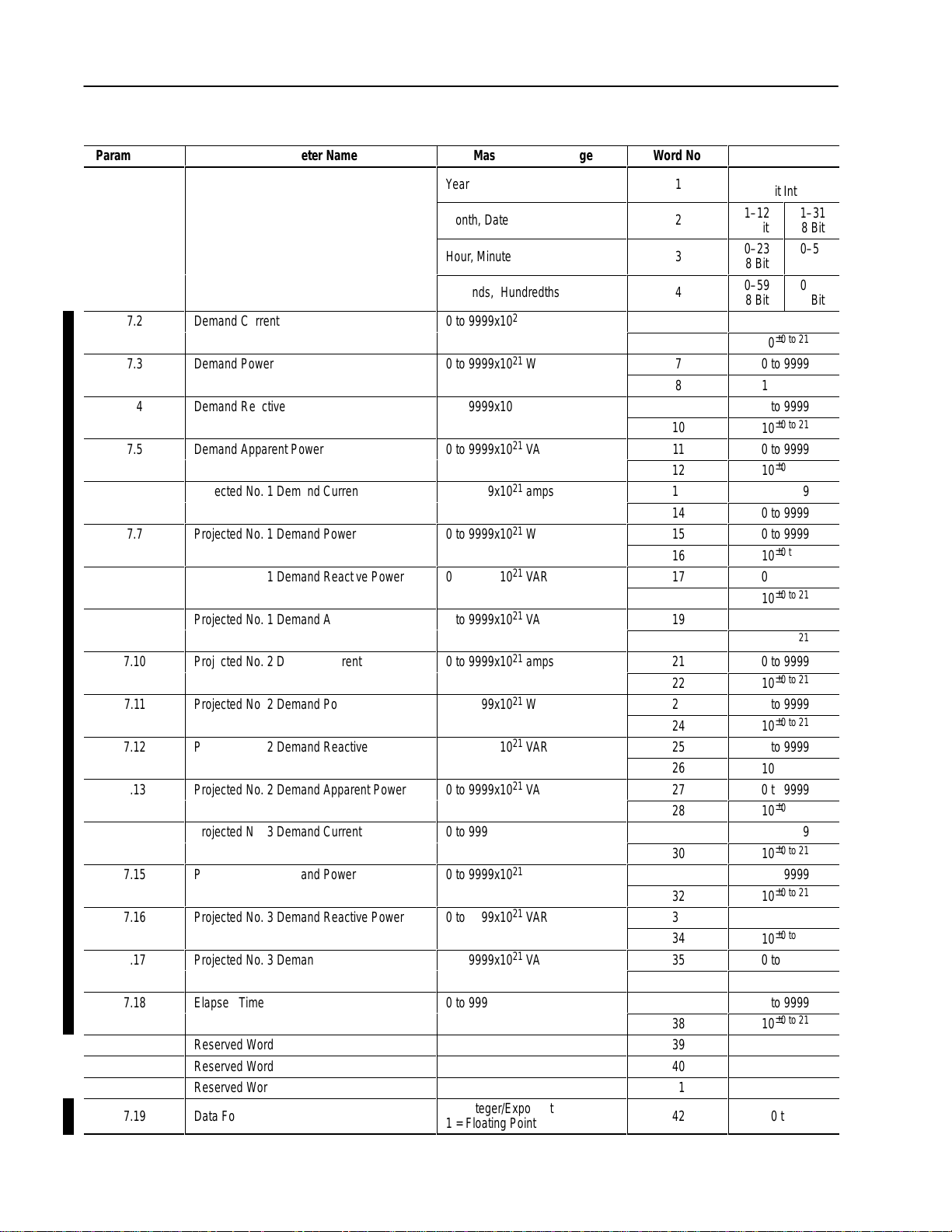
7.1
ÁÁÁ
Time Stamp
ББББББББББ
Parameter Name
Master Module Range
Year
БББББББ
Month, Date
ÁÁÁ
ÁÁÁÁББББББББББÁБББББББ
ББББББББББ
БББББББ
Hour, Minute
Seconds, Hundredths
ÁÁÁÁББББББББББÁБББББББ
7.2
7.3
7.4
7.5
7.6
7.7
7.8
7.9
7.10
7.11
ÁÁÁ
7.12
7.13
7.14
7.15
7.16
7.17
7.18
Demand Current
Demand Power
Demand Reactive Power
Demand Apparent Power
Projected No. 1 Demand Current
Projected No. 1 Demand Power
Projected No. 1 Demand Reactive Power
Projected No. 1 Demand Apparent Power
Projected No. 2 Demand Current
Projected No. 2 Demand Power
ББББББББББ
Projected No. 2 Demand Reactive Power
Projected No. 2 Demand Apparent Power
Projected No. 3 Demand Current
Projected No. 3 Demand Power
Projected No. 3 Demand Reactive Power
Projected No. 3 Demand Apparent Power
Elapsed Time
0 to 9999x1021 amps
0 to 9999x1021 W
0 to 9999x1021 VAR
0 to 9999x1021 VA
0 to 9999x1021 amps
0 to 9999x1021 W
0 to 9999x1021 VAR
0 to 9999x1021 VA
0 to 9999x1021 amps
0 to 9999x1021 W
БББББББ
0 to 9999x1021 VAR
0 to 9999x1021 VA
0 to 9999x1021 amps
0 to 9999x1021 W
0 to 9999x1021 VAR
0 to 9999x1021 VA
0 to 9999x10
21
Reserved Word
Reserved Word
Reserved Word
7.19
ÁÁÁ
Data Format
ББББББББББ
0 = Integer/Exponent
БББББББ
1 = Floating Point
Word No.
1
ÁÁÁ
ÁÁÁ2Á
3
ÁÁÁ
4
ÁÁÁ
5
6
7
8
9
10
11
12
13
14
15
16
17
18
19
20
21
22
ÁÁÁ23ÁÁÁÁ
24
25
26
27
28
29
30
31
32
33
34
35
36
37
38
Range
0–99
ÁÁÁÁ
16 Bit Integer
1–12
8 Bit
0–23
Á
8 Bit
0–59
8 Bit
Á
1–31
8 Bit
ÁÁ
0–59
ÁÁ
8 Bit
0–99
8 Bit
ÁÁ
0 to 9999
±
0 to 21
10
0 to 9999
±
0 to 21
10
0 to 9999
±
0 to 21
10
0 to 9999
±
0 to 21
10
0 to 9999
0 to 9999
0 to 9999
±
0 to 21
10
0 to 9999
±
0 to 21
10
0 to 9999
±
0 to 21
10
0 to 9999
±
0 to 21
10
0 to 9999
±
0 to 21
10
0 to 9999
±
0 to 21
10
0 to 9999
±
0 to 21
10
0 to 9999
±
0 to 21
10
0 to 9999
±
0 to 21
10
0 to 9999
±
0 to 21
10
0 to 9999
±
0 to 21
10
0 to 9999
±
0 to 21
10
39
40
41
42
ÁÁÁ
0 to 1
ÁÁÁÁ
Publication
1403-5.1
Page 21
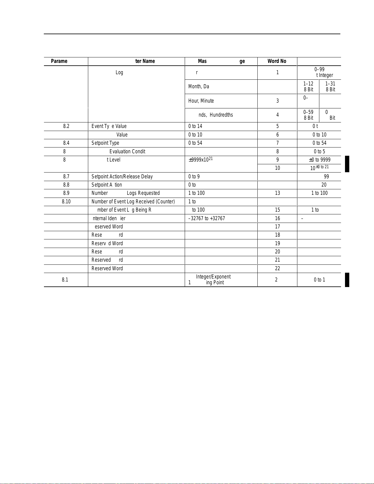
Table B.11 Event Log – Read
Á
Á
Á
Á
Á
Á
Á
Á
Á
Á
Á
Á
Á
Á
Á
Á
B–11Smart Communication Card Data Tables
Parameter No.
8.1
ÁÁÁÁ
Event Time Log Stamp
БББББББББ
Parameter Name
Master Module Range
Year
БББББББ
Month, Date
ÁÁÁÁ
ÁÁÁÁÁБББББББББÁБББББББ
БББББББББ
БББББББ
Hour, Minute
Seconds, Hundredths
ÁÁÁÁÁБББББББББÁБББББББ
8.2
8.3
8.4
8.5
8.6
8.7
8.8
8.9
8.10
8.11
8.12
Event Type Value
Event Code Value
Setpoint Type
Setpoint Evaluation Condition
Setpoint Level
Setpoint Action/Release Delay
Setpoint Action
Number of Event Logs Requested
Number of Event Log Received (Counter)
Number of Event Log Being Returned
Internal Identifier
0 to 14
0 to 10
0 to 54
0 to 5
9999x10
21
±
0 to 9999
0 to 20
1 to 100
1 to 100
1 to 100
–32767 to +32767
Reserved Word
Reserved Word
Reserved Word
Reserved Word
Reserved Word
Reserved Word
ÁÁÁÁ
8.13
БББББББББ
Data Format
0 = Integer/Exponent
БББББББ
1 = Floating Point
Word No.
1
ÁÁÁ
Range
ÁÁÁÁ
16 Bit Integer
1–12
ÁÁÁ2ÁÁ
3
ÁÁÁ
4
ÁÁÁ
5
6
7
8
9
10
11
12
13
14
15
16
8 Bit
0–23
ÁÁ
8 Bit
0–59
8 Bit
ÁÁ
0 to 14
0 to 10
0 to 54
0 to 5
±
0 to 9999
10
0 to 9999
0 to 20
1 to 100
1 to 100
1 to 100
–32767 to +32767
17
18
19
20
21
22
ÁÁÁ
23
ÁÁÁÁ
0 to 1
0–99
ÁÁ
ÁÁ
ÁÁ
±
0 to 21
1–31
8 Bit
0–59
8 Bit
0–99
8 Bit
Publication
1403-5.1
Page 22
B–12 Smart Communication Card Data Tables
Á
Á
Á
Á
Á
Á
Á
Á
Á
Á
Á
Á
Á
Table B.12 Voltage/Current/Miscellaneous Snapshot Log Data Table Read
Parameter No.
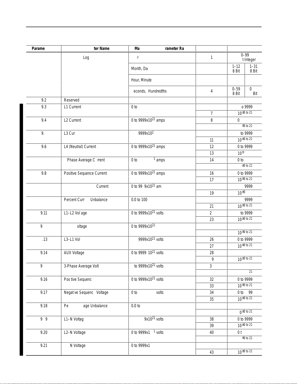
9.1
ÁÁÁÁ
Event Time Log Stamp
Parameter Name
ББББББББ
Master Module Parameter Range
Year
ББББББББ
Month, Date
ÁÁÁÁ
ÁÁÁÁÁББББББББÁББББББББ
ББББББББ
ББББББББ
Hour, Minute
Seconds, Hundredths
ÁÁÁÁÁББББББББÁББББББББ
9.2
9.3
9.4
Reserved
L1 Current
L2 Current
0 to 9999x1021 amps
0 to 9999x1021 amps
9.5
9.6
9.7
9.8
9.9
L3 Current
L4 (Neutral) Current
3-Phase Average Current
Positive Sequence Current
Negative Sequence Current
0 to 9999x1021 amps
0 to 9999x1021 amps
0 to 9999x1021 amps
0 to 9999x1021 amps
0 to 9999x1021 amps
9.10
9.11
ÁÁÁÁ
9.12
9.13
9.14
9.15
9.16
9.17
9.18
9.19
9.20
9.21
Percent Current Unbalance
L1–L2 Voltage
ББББББББ
L2–L3 Voltage
L3–L1 Voltage
AUX Voltage
3-Phase Average Voltage (L–L)
Positive Sequence Voltage
Negative Sequence Voltage
Percent Voltage Unbalance
L1–N Voltage
L2–N Voltage
L3–N Voltage
0.0 to 100.0
0 to 9999x1021 volts
ББББББББ
0 to 9999x1021 volts
0 to 9999x1021 volts
0 to 9999x1021 volts
0 to 9999x1021 volts
0 to 9999x1021 volts
0 to 9999x1021 volts
0.0 to 100.0
0 to 9999x1021 volts
0 to 9999x1021 volts
0 to 9999x1021 volts
Word No.
1
ÁÁÁ
ÁÁÁ2Á
3
ÁÁÁ
4
ÁÁÁ
Range
0–99
ÁÁÁÁ
16 Bit Integer
1–12
8 Bit
0–23
Á
8 Bit
0–59
8 Bit
Á
1–31
8 Bit
ÁÁ
0–59
ÁÁ
8 Bit
0–99
8 Bit
ÁÁ
5
6
7
8
9
10
11
12
13
14
15
16
17
18
19
20
21
22
ÁÁÁ23ÁÁÁÁ
24
25
26
27
28
29
30
31
32
33
34
35
36
37
38
39
40
41
42
43
0 to 9999
±
0 to 21
10
0 to 9999
±
0 to 21
10
0 to 9999
±
0 to 21
10
0 to 9999
±
0 to 21
10
0 to 9999
±
0 to 21
10
0 to 9999
±
0 to 21
10
0 to 9999
±
0 to 21
10
0 to 9999
±
0 to 21
10
0 to 9999
±
0 to 21
10
0 to 9999
±
0 to 21
10
0 to 9999
±
0 to 21
10
0 to 9999
±
0 to 21
10
0 to 9999
±
0 to 21
10
0 to 9999
±
0 to 21
10
0 to 9999
±
0 to 21
10
0 to 9999
±
0 to 21
10
0 to 9999
±
0 to 21
10
0 to 9999
±
0 to 21
10
0 to 9999
±
0 to 21
10
Publication
1403-5.1
Page 23
B–13Smart Communication Card Data Tables
Á
Á
Á
Á
Á
Á
Á
Á
Á
Á
Á
Á
Á
Á
Á
Á
Á
Á
Á
Á
Á
Á
Á
Parameter No.
9.22
Parameter Name
3–Phase Average Voltage (L–N)
Master Module Parameter Range
0 to 9999x1021 volts
Reserved
Reserved
9.23
Last Cycle Frequency
20.0 to 132.0
0 = No Rotation
9.24
ÁÁÁÁ
9.25
9.26
9.27
ÁÁÁÁ
9.28
Phase Rotation
ББББББББ
Number of Snapshot Logs Requested
Number of snapshot Log Received
(Counter)
Number of Snapshot Log Being
ББББББББ
Returned
Internal Identifier
1 = ABC
ББББББББ
2 = ACB
1 to 50
1 to 50
1 to 50
ББББББББ
–32767 to +32767
Table B.13 Power Snapshot Log Data Table
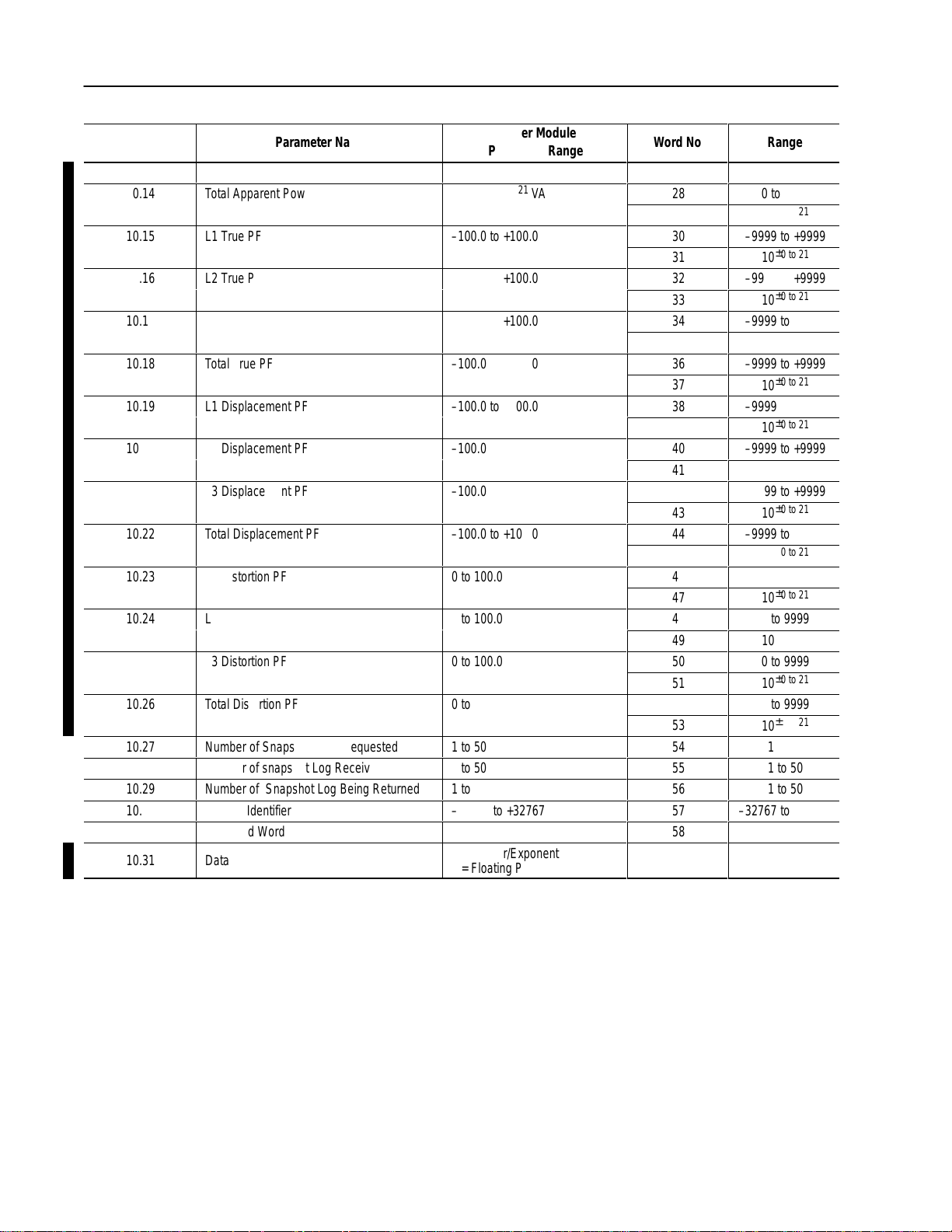
Parameter No.
ÁÁÁÁ
10.1
ÁÁÁÁ
БББББББББ
Event Time Log Stamp
БББББББББ
Parameter Name
Master Module
БББББББ
Parameter Range
Year
БББББББ
Month, Date
ÁÁÁÁÁБББББББББÁБББББББ
Hour, Minute
Seconds, Hundredths
10.2
10.3
10.4
10.5
10.6
10.7
10.8
10.9
10.10
10.11
10.12
10.13
Reserved Word
L1 Real Power
L2 Real Power
L3 Real Power
Total Real Power
L1 Reactive Power
L2 Reactive Power
L3 Reactive Power
Total Reactive Power
L1 Apparent Power
L2 Apparent Power
L3 Apparent Power
0 to 9999x1021 W
0 to 9999x10
21
W
0 to 9999x1021 W
0 to 9999x1021 W
0 to 9999x1021 VAR
0 to 9999x1021 VAR
0 to 9999x1021 VAR
0 to 9999x1021 VAR
0 to 9999x1021 VA
0 to 9999x1021 VA
0 to 9999x1021 VA
Word No.
44
45
46
47
48
49
50
ÁÁÁ
51
52
53
ÁÁÁ
54
Word No.
ÁÁÁ
1
ÁÁÁ
2
3
ÁÁÁ
4
5
6
7
8
9
10
11
12
13
14
15
16
17
18
19
20
21
22
23
24
25
26
Range
0 to 9999
±
0 to 21
10
0 to 9999
±
0 to 21
10
0 to 2
ÁÁÁÁ
1 to 50
1 to 50
1 to 50
ÁÁÁÁ
–32767 to +32767
Range
ÁÁÁÁ
0–99
16 Bit Integer
ÁÁÁÁ
1–12
8 Bit
0–23
8 Bit
ÁÁ
0–59
8 Bit
1–31
8 Bit
0–59
8 Bit
ÁÁ
0–59
8 Bit
0 to 9999
±
0 to 21
10
0 to 9999
±
0 to 21
10
0 to 9999
±
0 to 21
10
0 to 9999
±
0 to 21
10
0 to 9999
±
0 to 21
10
0 to 9999
±
0 to 21
10
0 to 9999
±
0 to 21
10
0 to 9999
±
0 to 21
10
0 to 9999
±
0 to 21
10
0 to 9999
±
0 to 21
10
0 to 9999
Publication
1403-5.1
Page 24
B–14 Smart Communication Card Data Tables
Parameter No.
10.14
10.15
10.16
10.17
10.18
10.19
10.20
10.21
10.22
10.23
10.24
10.25
10.26
ÁÁÁÁ
10.27
10.28
10.29
10.30
10.31
Parameter Name
Total Apparent Power
L1 True PF
L2 True PF
L3 True PF
Total True PF
L1 Displacement PF
L2 Displacement PF
L3 Displacement PF
Total Displacement PF
L1 Distortion PF
L2 Distortion PF
L3 Distortion PF
Total Distortion PF
БББББББББ
Number of Snapshot Logs Requested
Number of snapshot Log Received (Counter)
Number of Snapshot Log Being Returned
Internal Identifier
0 to 9999x1021 VA
–100.0 to +100.0
–100.0 to +100.0
–100.0 to +100.0
–100.0 to +100.0
–100.0 to +100.0
–100.0 to +100.0
–100.0 to +100.0
–100.0 to +100.0
0 to 100.0
0 to 100.0
0 to 100.0
0 to 100.0
БББББББ
1 to 50
1 to 50
1 to 50
–32767 to +32767
Reserved Word
Data Format
0 = Integer/Exponent
1 = Floating Point
Master Module
Parameter Range
Word No.
27
28
29
30
31
32
33
34
35
36
37
38
39
40
41
42
43
44
45
46
47
48
49
50
51
ÁÁÁ52ÁÁÁÁ
53
54
55
56
57
Range
±
0 to 21
10
0 to 9999
±
0 to 21
10
–9999 to +9999
±
0 to 21
10
–9999 to +9999
±
0 to 21
10
–9999 to +9999
±
0 to 21
10
–9999 to +9999
±
0 to 21
10
–9999 to +9999
±
0 to 21
10
–9999 to +9999
±
0 to 21
10
–9999 to +9999
±
0 to 21
10
–9999 to +9999
±
0 to 21
10
0 to 9999
±
0 to 21
10
0 to 9999
±
0 to 21
10
0 to 9999
±
0 to 21
10
0 to 9999
±
0 to 21
10
1 to 50
1 to 50
1 to 50
–32767 to +32767
58
59
0 to 1
Publication
1403-5.1
Page 25
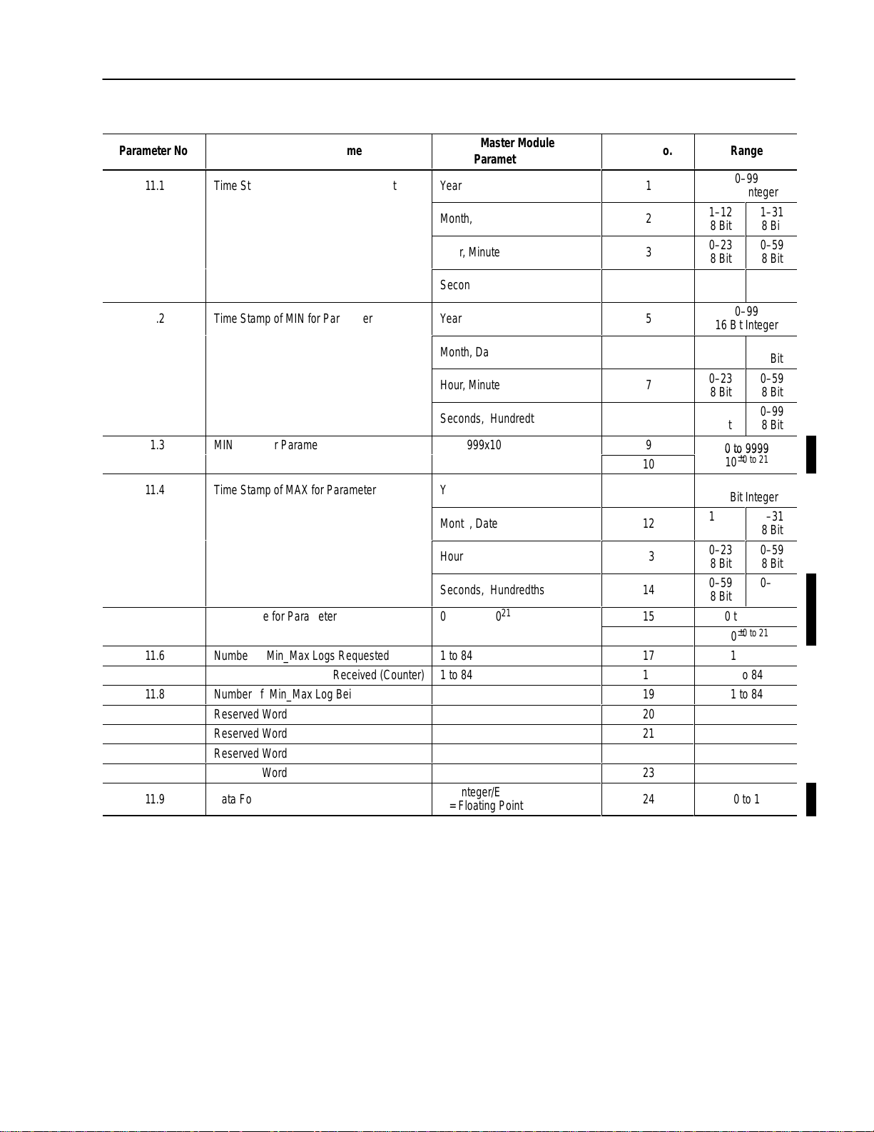
Table B.14 Min_Max Log – Read
Á
Á
Á
Á
Á
Á
Á
Á
Á
Á
Á
Á
Á
Á
Á
Á
0 to 9999
Á
Á
Á
Á
Á
Á
Á
Á
Á
Á
Á
Á
Á
B–15Smart Communication Card Data Tables
Parameter No.
11.1
ÁÁÁÁ
Parameter Name
Time Stamp of last Min/Max Log Reset
БББББББББ
Master Module
Parameter Range
Year
БББББББ
Month, Date
ÁÁÁÁÁБББББББББÁБББББББ
Hour, Minute
Seconds, Hundredths
11.2
ÁÁÁÁ
Time Stamp of MIN for Parameter
БББББББББ
Year
БББББББ
Month, Date
ÁÁÁÁÁБББББББББÁБББББББ
Hour, Minute
Seconds, Hundredths
11.3
11.4
ÁÁÁÁ
MIN Value for Parameter
Time Stamp of MAX for Parameter
БББББББББ
0 to 9999x10
Year
БББББББ
Month, Date
ÁÁÁÁÁБББББББББÁБББББББ
Hour, Minute
Seconds, Hundredths
11.5
11.6
11.7
11.8
MAX Value for Parameter
Number of Min_Max Logs Requested
Number of Min_Max Log Received (Counter)
Number of Min_Max Log Being Returned
0 to 9999x10
1 to 84
1 to 84
1 to 84
21
Reserved Word
Reserved Word
Reserved Word
Reserved Word
11.9
ÁÁÁÁ
Data Format
БББББББББ
0 = Integer/Exponent
1 = Floating Point
БББББББ
Word No.
1
ÁÁÁ
2
3
ÁÁÁ
4
5
ÁÁÁ
6
7
ÁÁÁ
8
9
10
11
ÁÁÁ
12
13
ÁÁÁ
14
15
16
17
18
19
20
21
22
23
24
ÁÁÁ
Range
0–99
16 Bit Integer
ÁÁÁÁ
1–12
8 Bit
0–23
ÁÁ
8 Bit
0–59
8 Bit
1–31
8 Bit
0–59
ÁÁ
8 Bit
0–99
8 Bit
0–99
ÁÁÁÁ
16 Bit Integer
1–12
8 Bit
0–23
ÁÁ
8 Bit
0–59
8 Bit
1–31
8 Bit
0–59
ÁÁ
8 Bit
0–99
8 Bit
0 to 9999
±
0 to 21
10
0–99
16 Bit Integer
ÁÁÁÁ
1–12
8 Bit
0–23
8 Bit
ÁÁ
0–59
8 Bit
1–31
8 Bit
0–59
8 Bit
ÁÁ
0–99
8 Bit
0 to 9999
±
0 to 21
10
1 to 84
1 to 84
1 to 84
0 to 1
ÁÁÁÁ
Publication
1403-5.1
Page 26

B–16 Smart Communication Card Data Tables
Á
Á
Á
Á
Á
Á
Á
Á
Á
Á
Á
Á
Á
Á
Á
Á
Á
Á
Á
Á
Á
Á
Á
Á
Á
Á
Á
Á
Á
Á
Table B.15 Log Selection Command Table Write
Param. No.
ÁÁÁÁ
12.1
ÁÁÁÁ
ÁÁÁÁ
12.2
ÁÁÁÁ
12.3
ÁÁÁÁ
12.4
ÁÁÁÁ
Parameter Name
ББББББББ
Selected Log
ББББББББ
ББББББББ
Requested Number of Data Sets
ББББББББ
Chronology of Returned Data
ББББББББ
First Min/Max Parameter to be
Returned
ББББББББ
Reserved Word
Reserved Word
Reserved Word
Reserved Word
Reserved Word
Master Module Range
23 = Event Log
ББББББББ
24 = Min/Max Log
54 = Snapshot V/I Log
ББББББББ
59 = Snapshot Power Log
1 to 100 for Event Log
1 to 84 for Min/Max Log
ББББББББ
1 to 50 for Snapshot V/I Log
ББББББББ
1 to 50 for Snapshot Power Log
0 = Reverse
1 = Forward
ББББББББ
Note: Not used for Min/Max Log
1 to 84
ББББББББ
Word No.
ÁÁÁ
1
ÁÁÁ
ÁÁÁ
2
ÁÁÁ
3
ÁÁÁ
4
ÁÁÁ
5
6
7
8
9
Range
ÁÁÁÁ
23, 24, 54, 59
ÁÁÁÁ
1 to 100
1 to 84
ÁÁÁÁ
1 to 50
ÁÁÁÁ
1 to 50
0 to 1
ÁÁÁÁ
1 to 84
ÁÁÁÁ
Publication
1403-5.1
Page 27

Table B.16 Available Min/Max Log Parameters (Identifiers for parameter 12.4)
Parameter Number
Parameter Description
1 Phase 1 Current
2 Phase 2 Current
3 Phase 3 Current
4 Phase 4 Current
5 Average Current
6 Positive Sequence Current
7 Negative Sequence Current
8 Current Unbalance
9 Phase 1 L–L Voltage
10 Phase 2 L–L Voltage
11 Phase 3 L–L Voltage
12 Auxiliary Voltage
13 Average L–L Voltage
14 Positive Sequence Voltage
15 Negative Sequence Voltage
16 Voltage Unbalance
17 Phase 1 L–N Voltage
18 Phase 2 L–N Voltage
19 Phase 3 L–N Voltage
20 Average L–N Voltage
21 Frequency
22 Phase 1 Real Power
23 Phase 2 Real Power
24 Phase 3 Real Power
25 Total Real Power
26 Phase 1 Reactive Power
27 Phase 2 Reactive Power
28 Phase 3 Reactive Power
29 Total Reactive Power
30 Phase 1 Apparent Power
31 Phase 2 Apparent Power
32 Phase 3 Apparent Power
33 Total Apparent Power
34 Phase 1 True Power Factor
35 Phase 2 True Power Factor
36 Phase 3 True Power Factor
37 Total True Power Factor
38 Phase 1 Displacement Power Factor
39 Phase 2 Displacement Power Factor
40 Phase 3 Displacement Power Factor
41 Total Displacement Power Factor
42 Phase 1 Distortion Power Factor
Parameter Number Parameter Description
43 Phase 2 Distortion Power Factor
44 Phase 3 Distortion Power Factor
45 Total Distortion Power Factor
46 Current Demand
47 Real Power Demand
48 Reactive Power Demand
49 Apparent Power Demand
50 Phase 1 Voltage IEEE THD
51 Phase 1 Voltage IEC THD
52
53
54
55 Phase 1 Current IEEE THD
56 Phase 1 Current IEC THD
57
58
59
60 Phase 2 Voltage IEEE THD
61 Phase 2 Voltage IEC THD
62
63
64
65 Phase 2 Current IEEE THD
66 Phase 2 Current IEC THD
67
68
69
70 Phase 3 Voltage IEEE THD
71 Phase 3 Voltage IEC THD
72
73
74
75 Phase 3 Current IEEE THD
76 Phase 3 Current IEC THD
77
78
79
80 Phase 4 Current IEEE THD
81 Phase 4 Current IEC THD
82
83
84
B–17Smart Communication Card Data Tables
Phase 1 Voltage TIF
Phase 1 Voltage Crest Factor
Phase 1 Voltage K-factor
Phase 1 Current TIF
Phase 1 Current Crest Factor
Phase 1 Current K-factor
Phase 2 Voltage TIF
Phase 2 Voltage Crest Factor
Phase 2 Voltage K-factor
Phase 2 Current TIF
Phase 2 Current Crest Factor
Phase 2 Current K-factor
Phase 3 Voltage TIF
Phase 3 Voltage Crest Factor
Phase 3 Voltage K-factor
Phase 3 Current TIF
Phase 3 Current Crest Factor
Phase 3 Current K-factor
Phase 4 Current TIF
Phase 4 Current Crest Factor
Phase 4 Current K-factor
①
①
①
①
①
①
①
①
①
①
①
①
①
①
①
①
①
①
①
①
①
➀
Not
available on 1403-LM.
Publication
1403-5.1
Page 28

B–18 Smart Communication Card Data Tables
Á
Á
Á
Á
Á
Á
Á
Á
Á
Á
Á
Á
Á
Á
Á
Á
Á
Á
Á
Á
Harmonic
Distortion T
ables – Read
Harmonic Distortion Data Tables for Channel 2 through Channel 7 are identical to the Even and Odd Harmonic
Distortion Tables for Channel 1. There are a total of 14 tables for this information.
(V1, V2, V3, I1, I2, I3, I4) The table sizes indicate this is Harmonic Distortion Data. The Channel Number designates
which one.
Table B.17 Even Harmonic Distortion Table – Channel 1
Parameter No.
13.1
13.2
13.3
ÁÁÁÁ
13.4
13.5
13.6
ÁÁÁÁ
13.7
ÁÁÁÁ
ÁÁÁÁ
13.8
13.9
13.10
13.11
13.12
13.13
13.14
13.15
13.16
13.17
13.18
IEEE Total Harmonic Distortion
IEC Total Harmonic Distortion
Meets IEEE 519
(Reserved 1403-LM)
TIF
(Reserved 1403-LM)
Crest Factor
(Reserved 1403-LM)
K-Factor
(Reserved 1403-LM)
Channel Number
Harmonic Distortion – Fundamental
(Reserved 1403-LM)
Harmonic Distortion – Second
(Reserved 1403-LM)
Harmonic Distortion – Fourth
(Reserved 1403-LM)
Harmonic Distortion – Sixth
(Reserved 1403-LM)
Harmonic Distortion – Eighth
(Reserved 1403-LM)
Harmonic Distortion – Tenth
(Reserved 1403-LM)
Harmonic Distortion – Twelfth
(Reserved 1403-LM)
Harmonic Distortion – Fourteenth
(Reserved 1403-LM)
Harmonic Distortion – Sixteenth
(Reserved 1403-LM)
Harmonic Distortion – Eighteenth
(Reserved 1403-LM)
Harmonic Distortion – Twentieth
(Reserved 1403-LM)
Parameter Name
ББББББББ
ББББББББ
ББББББББ
ББББББББ
Master Module Range
0 to 1000%
0 to 1000%
–1 = Unknown
0 = Fail
ББББББББ
1 = Pass
0 to 9999x10
0 to 9999x10
0 to 9999x10
21
21
21
1 = L1 Voltage
2 = L1 Current
ББББББББ
3 = L2 Voltage
4 = L2 Current
ББББББББ
5 = L3 Voltage
6 = L3 Current
ББББББББ
7 = L4 Current
0 to 1000%
0 to 1000%
0 to 1000%
0 to 1000%
0 to 1000 %
0 to 1000%
0 to 1000%
0 to 1000%
0 to 1000%
0 to 1000%
0 to 1000%
Word No.
1
2
3
4
5
ÁÁÁ
6
7
8
9
10
11
ÁÁÁ
12
ÁÁÁ
ÁÁÁ
13
14
15
16
17
18
19
20
21
22
23
24
25
26
27
28
29
30
31
32
33
34
Range
0 to 9999
±
0 to 21
10
0 to 9999
±
0 to 21
10
–1 to +1
ÁÁÁÁ
0 to 9999
±
0 to 21
10
0 to 9999
±
0 to 21
10
0 to 9999
±
0 to 21
10
ÁÁÁÁ
1 to 7
ÁÁÁÁ
ÁÁÁÁ
0 to 9999
±
0 to 21
10
0 to 9999
±
0 to 21
10
0 to 9999
±
0 to 21
10
0 to 9999
±
0 to 21
10
0 to 9999
±
0 to 21
10
0 to 9999
±
0 to 21
10
0 to 9999
±
0 to 21
10
0 to 9999
±
0 to 21
10
0 to 9999
±
0 to 21
10
0 to 9999
±
0 to 21
10
0 to 9999
±
0 to 21
10
Publication
1403-5.1
Page 29

B–19Smart Communication Card Data Tables
Á
Á
Á
Á
Á
Á
Á
Á
Á
Á
Á
Á
Á
Á
Á
Á
Á
Á
Á
Á
Parameter No.
13.19
Harmonic Distortion – Twenty-second
Parameter Name
(Reserved 1403-LM)
13.20
Harmonic Distortion – Twenty-fourth
(Reserved 1403-LM)
13.21
Harmonic Distortion – Twenty-sixth
(Reserved 1403-LM)
13.22
Harmonic Distortion – Twenty-eighth
(Reserved 1403-LM)
13.23
ÁÁÁÁ
13.24
Harmonic Distortion – Thirtieth
(Reserved 1403-LM)
ББББББББ
Harmonic Distortion – Thirty-second
(Reserved 1403-LM)
13.25
Harmonic Distortion – Thirty-fourth
(Reserved 1403-LM)
13.26
Harmonic Distortion – Thirty-sixth
(Reserved 1403-LM)
13.27
Harmonic Distortion – Thirty-eighth
(Reserved 1403-LM)
13.28
Harmonic Distortion – Fortieth
(Reserved 1403-LM)
13.29
FFT Chronological Reference Number
Reserved Word
Reserved Word
Reserved Word
Reserved Word
13.30
Data Format
Table B.18 Odd Harmonic Distortion Table – Channel 1
Parameter No.
14.1
14.2
14.3
ÁÁÁÁ
14.4
IEEE Total Harmonic Distortion
IEC Total Harmonic Distortion
Meets IEEE 519
(Reserved 1403-LM)
ББББББББ
TIF Value
Parameter Name
(Reserved 1403-LM)
14.5
Crest Factor
(Reserved 1403-LM)
14.6
K-Factor
(Reserved 1403-LM)
ÁÁÁÁ
14.7
ÁÁÁÁ
ÁÁÁÁ
14.8
ББББББББ
Channel Number
ББББББББ
ББББББББ
Harmonic Distortion – Fundamental
Master Module Range
0 to 1000%
0 to 1000%
0 to 1000%
0 to 1000%
0 to 1000%
ББББББББ
0 to 1000%
0 to 1000%
0 to 1000%
0 to 1000%
0 to 1000%
0 to 32767
0 = Integer/Exponent
1 = Floating Point
Master Module Range
0 to 1000%
0 to 1000%
–1 = Unknown
0 = Fail
1 = Pass
ББББББББ
0 to 9999x10
0 to 9999x10
0 to 9999x10
21
21
21
1 = L1 Voltage
2 = L1 Current
ББББББББ
3 = L2 Voltage
4 = L2 Current
ББББББББ
5 = L3 Voltage
6 = L3 Current
ББББББББ
7 = L4 Current
0 to 1000%
Word No.
35
36
37
38
39
40
41
42
43
ÁÁÁ44ÁÁÁÁ
45
46
47
48
49
50
51
52
53
54
55
Range
0 to 9999
±
0 to 21
10
0 to 9999
±
0 to 21
10
0 to 9999
±
0 to 21
10
0 to 9999
±
0 to 21
10
0 to 9999
±
0 to 21
10
0 to 9999
±
0 to 21
10
0 to 9999
±
0 to 21
10
0 to 9999
±
0 to 21
10
0 to 9999
±
0 to 21
10
0 to 9999
±
0 to 21
10
0 to 32767
56
57
58
59
60
Word No.
1
2
3
4
5
ÁÁÁ
6
7
8
9
10
11
ÁÁÁ
12
ÁÁÁ
ÁÁÁ
13
0 to 1
Range
0 to 9999
±
0 to 21
10
0 to 9999
±
0 to 21
10
–1 to +1
ÁÁÁÁ
0 to 9999
±
0 to 21
10
0 to 9999
±
0 to 21
10
0 to 9999
±
0 to 21
10
ÁÁÁÁ
1 to 7
ÁÁÁÁ
ÁÁÁÁ
0 to 9999
Publication
1403-5.1
Page 30

B–20 Smart Communication Card Data Tables
Á
Á
Á
Á
Á
Parameter No.
14.9
14.10
14.11
14.12
14.13
14.14
14.15
14.16
14.17
14.18
14.19
14.20
14.21
14.22
14.23
14.24
14.25
14.26
14.27
14.28
14.29
14.30
ÁÁÁÁ
Parameter Name
(Reserved 1403-LM)
Harmonic Distortion – Third
0 to 1000%
(Reserved 1403-LM)
Harmonic Distortion – Fifth
0 to 1000%
(Reserved 1403-LM)
Harmonic Distortion – Seventh
0 to 1000%
(Reserved 1403-LM)
Harmonic Distortion – Ninth
0 to 1000%
(Reserved 1403-LM)
Harmonic Distortion – Eleventh
0 to 1000%
(Reserved 1403-LM)
Harmonic Distortion – Thirteenth
0 to 1000%
(Reserved 1403-LM)
Harmonic Distortion – Fifteenth
0 to 1000%
(Reserved 1403-LM)
Harmonic Distortion – Seventeenth
0 to 1000%
(Reserved 1403-LM)
Harmonic Distortion – Nineteenth
0 to 1000%
(Reserved 1403-LM)
Harmonic Distortion – Twenty-first
0 to 1000%
(Reserved 1403-LM)
Harmonic Distortion – Twenty-third
0 to 1000%
(Reserved 1403-LM)
Harmonic Distortion – Twenty-fifth
0 to 1000%
(Reserved 1403-LM)
Harmonic Distortion – Twenty-seventh
0 to 1000%
(Reserved 1403-LM)
Harmonic Distortion – Twenty-ninth
0 to 1000%
(Reserved 1403-LM)
Harmonic Distortion – Thirty-first
0 to 1000%
(Reserved 1403-LM)
Harmonic Distortion – Thirty-third
0 to 1000%
(Reserved 1403-LM)
Harmonic Distortion – Thirty-fifth
0 to 1000%
(Reserved 1403-LM)
Harmonic Distortion – Thirty-seventh
0 to 1000%
(Reserved 1403-LM)
Harmonic Distortion – Thirty-ninth
0 to 1000%
(Reserved 1403-LM)
Harmonic Distortion – Forty-first
0 to 1000%
(Reserved 1403-LM)
FFT Chronological Reference Number
0 to 32767
Reserved Word
Reserved Word
Reserved Word
Reserved Word
Reserved Word
Data Format
ББББББББ
0 = Integer/Exponent
1 = Floating Point
Master Module Range
ББББББББ
Word No.
14
15
16
17
18
19
20
21
22
23
24
25
26
27
28
29
30
31
32
33
34
35
36
37
38
39
40
41
42
43
44
45
46
47
48
49
50
51
52
53
54
55
56
57
58
59
60
61
ÁÁÁ
Range
±
0 to 21
10
0 to 9999
±
0 to 21
10
0 to 9999
±
0 to 21
10
0 to 9999
±
0 to 21
10
0 to 9999
±
0 to 21
10
0 to 9999
±
0 to 21
10
0 to 9999
±
0 to 21
10
0 to 9999
±
0 to 21
10
0 to 9999
±
0 to 21
10
0 to 9999
±
0 to 21
10
0 to 9999
±
0 to 21
10
0 to 9999
±
0 to 21
10
0 to 9999
±
0 to 21
10
0 to 9999
±
0 to 21
10
0 to 9999
±
0 to 21
10
0 to 9999
±
0 to 21
10
0 to 9999
±
0 to 21
10
0 to 9999
±
0 to 21
10
0 to 9999
±
0 to 21
10
0 to 9999
±
0 to 21
10
0 to 9999
±
0 to 21
10
0 to 32767
0 to 1
ÁÁÁÁ
Publication
1403-5.1
Page 31

B–21Smart Communication Card Data Tables
Á
Á
Á
Á
Á
Á
Á
Á
Á
Á
Á
Á
Á
Á
Á
Á
Á
Á
Á
Á
Á
Á
Á
Á
Á
Harmonic
Magnitude Data T
ables for Channel 2 through Channel 7 are identical to the Even and Odd Harmonic
Magnitude Tables for Channel 1. There are a total of 14 tables for this information. (V1, V2, V3, I1, I2, I3, I4)
Table B.19 Even Harmonic Magnitude Data Table Channel 1
Parameter No.
15.1
15.2
15.3
ÁÁÁÁ
15.4
15.5
15.6
ÁÁÁÁ
ÁÁÁÁ
15.7
ÁÁÁÁ
ÁÁÁÁ
15.8
15.9
15.10
15.11
15.12
15.13
15.14
15.15
15.16
15.17
15.18
15.19
IEEE Total Harmonic Distortion
IEC Total Harmonic Distortion
Meets IEEE 519
(Reserved 1403-LM)
ББББББББ
TIF Value
(Reserved 1403-LM)
Crest Factor
(Reserved 1403-LM)
K-Factor
(Reserved 1403-LM)
ББББББББ
ББББББББ
Channel Number
ББББББББ
ББББББББ
Harmonic Magnitude – Fundamental
(Reserved 1403-LM)
Harmonic Magnitude – Second
(Reserved 1403-LM)
Harmonic Magnitude – Fourth
(Reserved 1403-LM)
Harmonic Magnitude – Sixth
(Reserved 1403-LM)
Harmonic Magnitude – Eighth
(Reserved 1403-LM)
Harmonic Magnitude – Tenth
(Reserved 1403-LM)
Harmonic Magnitude – Twelfth
(Reserved 1403-LM)
Harmonic Magnitude – Fourteenth
(Reserved 1403-LM)
Harmonic Magnitude – Sixteenth
(Reserved 1403-LM)
Harmonic Magnitude – Eighteenth
(Reserved 1403-LM)
Harmonic Magnitude – Twentieth
(Reserved 1403-LM)
Harmonic Magnitude – Twenty-second
(Reserved 1403-LM)
Parameter Name
Master Module Range
0 to 1000%
0 to 1000%
–1 = Unknown
0 = Fail
ББББББББ
1 = Pass
0 to 9999x10
0 to 9999x10
0 to 9999x10
1 = L1 Voltage
ББББББББ
2 = L1 Current
3 = L2 Voltage
ББББББББ
4 = L2 Current
5 = L3 Voltage
ББББББББ
6 = L3 Current
ББББББББ
7 = L4 Current
0 to 9999x10
0 to 9999x10
0 to 9999x10
0 to 9999x10
0 to 9999x10
0 to 9999x10
0 to 9999x10
0 to 9999x10
0 to 9999x10
0 to 9999x10
0 to 9999x10
0 to 9999x10
21
21
21
21
21
21
21
21
21
21
21
21
21
21
21
Word No.
1
2
3
4
5
ÁÁÁ
6
7
8
9
10
11
ÁÁÁ
ÁÁÁ
12
ÁÁÁ
ÁÁÁ
13
14
15
16
17
18
19
20
21
22
23
24
25
26
27
28
29
30
31
32
33
34
35
36
ÁÁÁÁ
ÁÁÁÁ
ÁÁÁÁ
ÁÁÁÁ
ÁÁÁÁ
Range
0 to 9999
±
0 to 21
10
0 to 9999
±
0 to 21
10
–1 to +1
0 to 9999
±
0 to 21
10
0 to 9999
±
0 to 21
10
0 to 9999
±
0 to 21
10
1 to 7
0 to 9999
±
0 to 21
10
0 to 9999
±
0 to 21
10
0 to 9999
±
0 to 21
10
0 to 9999
±
0 to 21
10
0 to 9999
±
0 to 21
10
0 to 9999
±
0 to 21
10
0 to 9999
±
0 to 21
10
0 to 9999
±
0 to 21
10
0 to 9999
±
0 to 21
10
0 to 9999
±
0 to 21
10
0 to 9999
±
0 to 21
10
0 to 9999
±
0 to 21
10
Publication
1403-5.1
Page 32

B–22 Smart Communication Card Data Tables
Á
Á
Á
Á
Á
Á
Á
Á
Á
Á
Á
Á
Á
Á
Á
Á
Á
Á
Á
Á
Á
Á
Á
Á
Á
Á
Á
Á
Á
Á
Parameter No.
15.20
15.21
15.22
15.23
15.24
ÁÁÁÁ
15.25
15.26
15.27
15.28
15.29
15.30
ÁÁÁÁ
Parameter Name
Harmonic Magnitude – Twenty-fourth
(Reserved 1403-LM)
Harmonic Magnitude – Twenty-sixth
(Reserved 1403-LM)
Harmonic Magnitude – Twenty-eighth
(Reserved 1403-LM)
Harmonic Magnitude – Thirtieth
(Reserved 1403-LM)
Harmonic Magnitude – Thirty-second
(Reserved 1403-LM)
ББББББББ
Harmonic Magnitude – Thirty-fourth
(Reserved 1403-LM)
Harmonic Magnitude – Thirty-sixth
(Reserved 1403-LM)
Harmonic Magnitude – Thirty-eighth
(Reserved 1403-LM)
Harmonic Magnitude – Fortieth
(Reserved 1403-LM)
FFT Update Reference Number
Reserved Word
Reserved Word
Data Format
ББББББББ
Master Module Range
0 to 9999x10
0 to 9999x10
0 to 9999x10
0 to 9999x10
0 to 9999x10
ББББББББ
0 to 9999x10
0 to 9999x10
0 to 9999x10
0 to 9999x10
21
21
21
21
21
21
21
21
21
0 to 32767
0 = Integer/Exponent
ББББББББ
1 = Floating Point
Word No.
37
38
39
40
41
42
43
44
45
ÁÁÁ46ÁÁÁÁ
47
48
49
50
51
52
53
54
55
Range
0 to 9999
±
0 to 21
10
0 to 9999
±
0 to 21
10
0 to 9999
±
0 to 21
10
0 to 9999
±
0 to 21
10
0 to 9999
±
0 to 21
10
0 to 9999
±
0 to 21
10
0 to 9999
±
0 to 21
10
0 to 9999
±
0 to 21
10
0 to 9999
±
0 to 21
10
0 to 32767
56
57
58
ÁÁÁ
0 t o 1
ÁÁÁÁ
Table B.20 Odd Harmonic Magnitude Data Table
Parameter No.
16.1
16.2
16.3
ÁÁÁÁ
16.4
IEEE Total Harmonic Distortion
IEC Total Harmonic Distortion
Meets IEEE 519
(Reserved 1403-LM)
TIF Value
Parameter Name
ББББББББ
(Reserved 1403-LM)
16.5
Crest Factor
(Reserved 1403-LM)
16.6
K-Factor
(Reserved 1403-LM)
ÁÁÁÁ
ÁÁÁÁ
16.7
ÁÁÁÁ
ÁÁÁÁ
16.8
ББББББББ
ББББББББ
Channel Number
ББББББББ
ББББББББ
Harmonic Magnitude – Fundamental
(Reserved 1403-LM)
Publication
16.9
1403-5.1
Harmonic Magnitude – Third
(Reserved 1403-LM)
Master Module Range
0 to 1000%
0 to 1000%
–1 = Unknown
0 = Fail
ББББББББ
1 = Pass
0 to 9999x10
0 to 9999x10
0 to 9999x10
21
21
21
1 = L1 Voltage
ББББББББ
2 = L1 Current
3 = L2 Voltage
ББББББББ
4 = L2 Current
5 = L3 Voltage
ББББББББ
6 = L3 Current
ББББББББ
7 = L4 Current
0 to 9999x10
0 to 9999x10
21
21
Word No.
1
2
3
4
5
ÁÁÁ
6
7
8
9
10
11
ÁÁÁ
ÁÁÁ
12
ÁÁÁ
ÁÁÁ
13
14
15
16
Range
0 to 9999
±
0 to 21
10
0 to 9999
±
0 to 21
10
–1 to +1
ÁÁÁÁ
0 to 9999
±
0 to 21
10
0 to 9999
±
0 to 21
10
0 to 9999
±
0 to 21
10
ÁÁÁÁ
ÁÁÁÁ
1 to 7
ÁÁÁÁ
ÁÁÁÁ
0 to 9999
±
0 to 21
10
0 to 9999
±
0 to 21
10
Page 33

B–23Smart Communication Card Data Tables
Á
Á
Á
Á
Á
Parameter No.
16.10
16.11
16.12
16.13
16.14
ÁÁÁÁ
16.15
16.16
16.17
16.18
16.19
16.20
16.21
16.22
16.23
16.24
16.25
16.26
16.27
16.28
16.29
16.30
ÁÁÁÁ
Parameter Name
Harmonic Magnitude – Fifth
0 to 9999x10
(Reserved 1403-LM)
Harmonic Magnitude – Seventh
0 to 9999x10
(Reserved 1403-LM)
Harmonic Magnitude – Ninth
0 to 9999x10
(Reserved 1403-LM)
Harmonic Magnitude – Eleventh
0 to 9999x10
(Reserved 1403-LM)
Harmonic Magnitude – Thirteenth
(Reserved 1403-LM)
ББББББББ
Harmonic Magnitude – Fifteenth
0 to 9999x10
ББББББББ
0 to 9999x10
(Reserved 1403-LM)
Harmonic Magnitude – Seventeenth
0 to 9999x10
(Reserved 1403-LM)
Harmonic Magnitude – Nineteenth
0 to 9999x10
(Reserved 1403-LM)
Harmonic Magnitude – Twenty-first
0 to 9999x10
(Reserved 1403-LM)
Harmonic Magnitude – Twenty-third
0 to 9999x10
(Reserved 1403-LM)
Harmonic Magnitude – Twenty-fifth
0 to 9999x10
(Reserved 1403-LM)
Harmonic Magnitude – Twenty-seventh
0 to 9999x10
(Reserved 1403-LM)
Harmonic Magnitude – Twenty-ninth
0 to 9999x10
(Reserved 1403-LM)
Harmonic Magnitude – Thirty-first
0 to 9999x10
(Reserved 1403-LM)
Harmonic Magnitude – Thirty-third
0 to 9999x10
(Reserved 1403-LM)
Harmonic Magnitude – Thirty-fifth
0 to 9999x10
(Reserved 1403-LM)
Harmonic Magnitude – Thirty-seventh
0 to 9999x10
(Reserved 1403-LM)
Harmonic Magnitude – Thirty-ninth
0 to 9999x10
(Reserved 1403-LM)
Harmonic Magnitude – Forty-first
0 to 9999x10
(Reserved 1403-LM)
FFT Chronological Reference Number
0 to 32767
Reserved Word
Data Format
ББББББББ
0 = Integer/Exponent
1 = Floating Point
ББББББББ
Master Module Range
21
21
21
21
21
21
21
21
21
21
21
21
21
21
21
21
21
21
21
Word No.
17
18
19
20
21
22
23
24
25
ÁÁÁ26ÁÁÁÁ
27
28
29
30
31
32
33
34
35
36
37
38
39
40
41
42
43
44
45
46
47
48
49
50
51
52
53
54
55
Range
0 to 9999
±
0 to 21
10
0 to 9999
±
0 to 21
10
0 to 9999
±
0 to 21
10
0 to 9999
±
0 to 21
10
0 to 9999
±
0 to 21
10
0 to 9999
±
0 to 21
10
0 to 9999
±
0 to 21
10
0 to 9999
±
0 to 21
10
0 to 9999
±
0 to 21
10
0 to 9999
±
0 to 21
10
0 to 9999
±
0 to 21
10
0 to 9999
±
0 to 21
10
0 to 9999
±
0 to 21
10
0 to 9999
±
0 to 21
10
0 to 9999
±
0 to 21
10
0 to 9999
±
0 to 21
10
0 to 9999
±
0 to 21
10
0 to 9999
±
0 to 21
10
0 to 9999
±
0 to 21
10
0 to 32767
56
57
ÁÁÁ
0 to 1
ÁÁÁÁ
Publication
1403-5.1
Page 34

B–24 Smart Communication Card Data Tables
Á
Á
Á
Á
Á
Á
Á
Á
Á
Á
Á
Á
Á
Á
Á
Á
Á
Á
Á
Á
Harmonic
Phase Angle Data T
ables for Channel 2 through Channel 7 are identical to the Even and Odd Harmonic Phase
Angle Data Tables for Channel 1. There are a total of 14 tables for this information.
(V1, V2, V3, I1, I2, I3, I4)
Table B.21 Even Harmonic Phase Angle Data Table Channel 1
Parameter No.
ÁÁÁÁ
ÁÁÁÁ
17.7
ÁÁÁÁ
ÁÁÁÁ
17.8
17.9
17.10
ÁÁÁÁ
17.11
17.12
17.13
17.14
17.15
17.16
17.17
17.18
17.19
17.20
Publication
1403-5.1
Reserved Word
Reserved Word
Reserved Word
Reserved Word
Reserved Word
Reserved Word
Reserved Word
Reserved Word
Reserved Word
Reserved Word
Reserved Word
ББББББББ
ББББББББ
Channel Number
(Reserved 1403-LM)
ББББББББ
ББББББББ
Harmonic Phase Angle – Fundamental
(Reserved 1403-LM)
Harmonic Phase Angle – Second
(Reserved 1403-LM)
Harmonic Phase Angle – Fourth
ББББББББ
(Reserved 1403-LM)
Harmonic Phase Angle – Sixth
(Reserved 1403-LM)
Harmonic Phase Angle – Eighth
(Reserved 1403-LM)
Harmonic Phase Angle – Tenth
(Reserved 1403-LM)
Harmonic Phase Angle – Twelfth
(Reserved 1403-LM)
Harmonic Phase Angle – Fourteenth
(Reserved 1403-LM)
Harmonic Phase Angle – Sixteenth
(Reserved 1403-LM)
Harmonic Phase Angle – Eighteenth
(Reserved 1403-LM)
Harmonic Phase Angle – Twentieth
(Reserved 1403-LM)
Harmonic Phase Angle – Twenty-second
(Reserved 1403-LM)
Harmonic Phase Angle – Twenty-fourth
(Reserved 1403-LM)
Parameter Name
Master Module Range
1 = L1 Voltage
ББББББББ
2 = L1 Current
3 = L2 Voltage
ББББББББ
4 = L2 Current
ББББББББ
5 = L3 Voltage
6 = L3 Current
ББББББББ
7 = L4 Current
0 to 360 degrees
0 to 360 degrees
0 to 360 degrees
ББББББББ
0 to 360 degrees
0 to 360 degrees
0 to 360 degrees
0 to 360 degrees
0 to 360 degrees
0 to 360 degrees
0 to 360 degrees
0 to 360 degrees
0 to 360 degrees
0 to 360 degrees
Word No.
1
2
3
4
5
6
7
8
9
10
11
ÁÁÁ
ÁÁÁ
12
ÁÁÁ
ÁÁÁ
13
14
15
16
ÁÁÁ17ÁÁÁÁ
18
19
20
21
22
23
24
25
26
27
28
29
30
31
32
33
34
35
36
37
38
Range
0 to 9999
±
0 to 21
10
0 to 9999
±
0 to 21
10
0 –1
0 to 9999
±
0 to 21
10
0 to 9999
±
0 to 21
10
0 to 9999
±
0 to 21
10
ÁÁÁÁ
ÁÁÁÁ
1 to 7
ÁÁÁÁ
ÁÁÁÁ
0 to 9999
±
0 to 21
10
0 to 9999
±
0 to 21
10
0 to 9999
±
0 to 21
10
0 to 9999
±
0 to 21
10
0 to 9999
±
0 to 21
10
0 to 9999
±
0 to 21
10
0 to 9999
±
0 to 21
10
0 to 9999
±
0 to 21
10
0 to 9999
±
0 to 21
10
0 to 9999
±
0 to 21
10
0 to 9999
±
0 to 21
10
0 to 9999
±
0 to 21
10
0 to 9999
±
0 to 21
10
Page 35

B–25Smart Communication Card Data Tables
Á
Á
Á
Á
Á
Á
Á
Á
Á
Á
Á
Á
Á
Á
Á
Á
Á
Á
Á
Á
Parameter No.
17.21
Harmonic Phase Angle – Twenty-sixth
Parameter Name
(Reserved 1403-LM)
17.22
Harmonic Phase Angle – Twenty-eighth
(Reserved 1403-LM)
17.23
Harmonic Phase Angle – Thirtieth
(Reserved 1403-LM)
17.24
Harmonic Phase Angle – Thirty-second
(Reserved 1403-LM)
17.25
ÁÁÁÁ
17.26
Harmonic Phase Angle – Thirty-fourth
(Reserved 1403-LM)
ББББББББ
Harmonic Phase Angle – Thirty-sixth
(Reserved 1403-LM)
17.27
Harmonic Phase Angle – Thirty-eighth
(Reserved 1403-LM)
17.28
Harmonic Phase Angle – Fortieth
(Reserved 1403-LM)
17.29
17.30
FFT Chronological Reference Number
Data Format
Table B.22 Odd Harmonic Phase Angle Data Table
Master Module Range
0 to 360 degrees
0 to 360 degrees
0 to 360 degrees
0 to 360 degrees
0 to 360 degrees
ББББББББ
0 to 360 degrees
0 to 360 degrees
0 to 360 degrees
0 to 32767
0 = Integer/Exponent
1 = Floating Point
Word No.
39
40
41
42
43
44
45
46
47
ÁÁÁ48ÁÁÁÁ
49
50
51
52
53
54
55
56
Range
0 to 9999
±
0 to 21
10
0 to 9999
±
0 to 21
10
0 to 9999
±
0 to 21
10
0 to 9999
±
0 to 21
10
0 to 9999
±
0 to 21
10
0 to 9999
±
0 to 21
10
0 to 9999
±
0 to 21
10
0 to 9999
±
0 to 21
10
0 to 32767
0 to 1
Parameter No.
ÁÁÁÁ
ÁÁÁÁ
ÁÁÁÁ
ÁÁÁÁ
18.7
18.8
18.9
18.10
18.11
18.12
Parameter Name
Reserved Word
Reserved Word
Reserved Word
Reserved Word
Reserved Word
Reserved Word
Reserved Word
Reserved Word
Reserved Word
Reserved Word
Reserved Word
Channel Number
БББББББББ
(Reserved 1403-LM)
БББББББББ
БББББББББ
БББББББББ
Harmonic Phase Angle – Fundamental
(Reserved 1403-LM)
Harmonic Phase Angle – Third
(Reserved 1403-LM)
Harmonic Phase Angle – Fifth
(Reserved 1403-LM)
Harmonic Phase Angle – Seventh
(Reserved 1403-LM)
Harmonic Phase Angle – Ninth
Master Module Range
1 = L1 Voltage
БББББББ
2 = L1 Current
3 = L2 Voltage
БББББББ
4 = L2 Current
БББББББ
5 = L3 Voltage
6 = L3 Current
БББББББ
7 = L4 Current
0 to 360 degrees
0 to 360 degrees
0 to 360 degrees
0 to 360 degrees
0 to 360 degrees
Word No.
1
2
3
4
5
6
7
8
9
10
11
12
ÁÁÁ
ÁÁÁ
ÁÁÁ
ÁÁÁ
13
14
15
16
17
18
19
20
21
Range
0 to 9999
±
0 to 21
10
0 to 9999
±
0 to 21
10
0 –1
0 to 9999
±
0 to 21
10
0 to 9999
±
0 to 21
10
0 to 9999
±
0 to 21
10
1 to 7
ÁÁÁÁ
ÁÁÁÁ
ÁÁÁÁ
ÁÁÁÁ
0 to 9999
±
0 to 21
10
0 to 9999
±
0 to 21
10
0 to 9999
±
0 to 21
10
0 to 9999
±
0 to 21
10
0 to 9999
Publication
1403-5.1
Page 36

B–26 Smart Communication Card Data Tables
Parameter No.
18.13
18.14
18.15
18.16
18.17
ÁÁÁÁ
18.18
18.19
18.20
18.21
18.22
18.23
18.24
18.25
18.26
18.27
18.28
18.29
Parameter Name
(Reserved 1403-LM)
Harmonic Phase Angle – Eleventh
(Reserved 1403-LM)
Harmonic Phase Angle – Thirteenth
(Reserved 1403-LM)
Harmonic Phase Angle – Fifteenth
(Reserved 1403-LM)
Harmonic Phase Angle – Seventeenth
(Reserved 1403-LM)
Harmonic Phase Angle – Nineteenth
БББББББББ
ББББББББ
(Reserved 1403-LM)
Harmonic Phase Angle – Twenty-first
(Reserved 1403-LM)
Harmonic Phase Angle – Twenty-third
(Reserved 1403-LM)
Harmonic Phase Angle – Twenty-fifth
(Reserved 1403-LM)
Harmonic Phase Angle – Twenty-seventh
(Reserved 1403-LM)
Harmonic Phase Angle – Twenty-ninth
(Reserved 1403-LM)
Harmonic Phase Angle – Thirty-first
(Reserved 1403-LM)
Harmonic Phase Angle – Thirty-third
(Reserved 1403-LM)
Harmonic Phase Angle – Thirty-fifth
(Reserved 1403-LM)
Harmonic Phase Angle – Thirty-seventh
(Reserved 1403-LM)
Harmonic Phase Angle – Thirty-ninth
(Reserved 1403-LM)
Harmonic Phase Angle – Forty-first
(Reserved 1403-LM)
FFT Chronological Reference Number
Master Module Range
0 to 360 degrees
0 to 360 degrees
0 to 360 degrees
0 to 360 degrees
0 to 360 degrees
0 to 360 degrees
0 to 360 degrees
0 to 360 degrees
0 to 360 degrees
0 to 360 degrees
0 to 360 degrees
0 to 360 degrees
0 to 360 degrees
0 to 360 degrees
0 to 360 degrees
0 to 360 degrees
0 to 32767
Word No.
22
23
24
25
26
27
28
29
30
ÁÁÁ31ÁÁÁÁ
32
33
34
35
36
37
38
39
40
41
42
43
44
45
46
47
48
49
50
51
52
53
54
55
Range
±
0 to 21
10
0 to 9999
±
0 to 21
10
0 to 9999
±
0 to 21
10
0 to 9999
±
0 to 21
10
0 to 9999
±
0 to 21
10
0 to 9999
±
0 to 21
10
0 to 9999
±
0 to 21
10
0 to 9999
±
0 to 21
10
0 to 9999
±
0 to 21
10
0 to 9999
±
0 to 21
10
0 to 9999
±
0 to 21
10
0 to 9999
±
0 to 21
10
0 to 9999
±
0 to 21
10
0 to 9999
±
0 to 21
10
0 to 9999
±
0 to 21
10
0 to 9999
±
0 to 21
10
0 to 9999
±
0 to 21
10
0 to 32767
Publication
1403-5.1
Page 37

B–27Smart Communication Card Data Tables
Á
Á
Á
Á
Á
Á
Á
Á
Á
Á
Á
Á
Á
Á
Á
Á
Á
Á
Á
Á
Á
Á
Á
Á
Á
Á
Á
Á
Á
Á
Á
Á
Á
Á
Á
Á
Á
Á
Á
Á
Á
Á
Á
Á
Á
Á
Á
Á
Á
Á
Á
Á
Á
Á
Á
Á
Á
Á
Á
Á
Á
Á
Table B.23 Oscillogram Capture Data – Read (54 Reads of 48 data points for 2-channel 12-cycle oscillogram or 9 Reads of 48 data points
for 7-channel 2-cycle oscillogram)
Parameter No.
ÁÁÁÁ
19.1
ÁÁÁÁÁБББББББББББ
БББББББББББ
Time Stamp of Oscillogram
(Reserved 1403-LM)
Parameter Name
Master Module
БББББ
Year
Month, Date
БББББ
Hour, Minute
ÁÁÁÁÁБББББББББББÁБББББ
Seconds, Hundredths
1 = L1 Voltage
ÁÁÁÁ
ÁÁÁÁ
ÁÁÁÁ
ÁÁÁÁ
ÁÁÁÁ
ÁÁÁÁ
ÁÁÁÁ
ÁÁÁÁ
ÁÁÁÁ
ÁÁÁÁ
19.2
19.3
19.4
19.5
19.6
19.7
19.8
19.9
19.10
19.11
19.12
19.13
19.14
19.15
19.16
19.17
19.18
19.19
19.20
19.21
19.22
19.23
19.24
19.25
19.26
19.27
БББББББББББ
БББББББББББ
Channel Number
(Reserved 1403-LM)
БББББББББББ
БББББББББББ
БББББББББББ
Channel Data Count (Reserved 1403-LM)
Oscillogram Chronological Reference Number
(Reserved 1403-LM)
БББББББББББ
Oscillogram Block Number (Reserved 1403-LM)
БББББББББББ
БББББББББББ
Actual Channel Numer
(Reserved 1403-LM)
БББББББББББ
БББББББББББ
Oscillogram Data Point 1 (Reserved 1403-LM)
Oscillogram Data Point 2 (Reserved 1403-LM)
Oscillogram Data Point 3 (Reserved 1403-LM)
Oscillogram Data Point 4 (Reserved 1403-LM)
Oscillogram Data Point 5 (Reserved 1403-LM)
Oscillogram Data Point 6 (Reserved 1403-LM)
Oscillogram Data Point 7 (Reserved 1403-LM)
Oscillogram Data Point 8 (Reserved 1403-LM)
Oscillogram Data Point 9 (Reserved 1403-LM)
Oscillogram Data Point 10 (Reserved 1403-LM)
Oscillogram Data Point 11 (Reserved 1403-LM)
Oscillogram Data Point 12 (Reserved 1403-LM)
Oscillogram Data Point 13 (Reserved 1403-LM)
Oscillogram Data Point 14 (Reserved 1403-LM)
Oscillogram Data Point 15 (Reserved 1403-LM)
Oscillogram Data Point 16 (Reserved 1403-LM)
Oscillogram Data Point 17 (Reserved 1403-LM)
Oscillogram Data Point 18 (Reserved 1403-LM)
Oscillogram Data Point 19 (Reserved 1403-LM)
Oscillogram Data Point 20 (Reserved 1403-LM)
Oscillogram Data Point 21 (Reserved 1403-LM)
2 = L1 Current
БББББ
3 = L2 Voltage
4 = L2 Current
БББББ
5 = L3 Voltage
БББББ
6 = L3 Current
7 = L4 Current
БББББ
8 = Ch A 12-Cycle
9 = Ch B 12-Cycle
БББББ
for 2-cycle 432
for 12-cycle 2592
0 to +32767
БББББ
1 to 54
1 = L1 Voltage
БББББ
2 = L1 Current
3 = L2 Voltage
БББББ
4 = L2 Current
БББББ
5 = L3 Voltage
6 = L3 Current
БББББ
7 = L4 Current
±
5000
±
5000
±
5000
±
5000
±
5000
±
5000
±
5000
±
5000
±
5000
±
5000
±
5000
±
5000
±
5000
±
5000
±
5000
±
5000
±
5000
±
5000
±
5000
±
5000
±
5000
Range
Word No.
ÁÁÁ
1
2
ÁÁÁ
3
4
ÁÁÁ
ÁÁÁ
ÁÁÁ
5
ÁÁÁ
ÁÁÁ
ÁÁÁ
6
7
ÁÁÁ
8
ÁÁÁ
ÁÁÁ
9
ÁÁÁ
ÁÁÁ
10
11
12
13
14
15
16
17
18
19
20
21
22
23
24
25
26
27
28
29
30
Range
ÁÁÁÁ
0–99
16 Bit Integer
1–12
ÁÁ
8 Bit
0–23
8 Bit
0–59
ÁÁ
8 Bit
ÁÁÁÁ
ÁÁÁÁ
ÁÁÁÁ
ÁÁÁÁ
ÁÁÁÁ
ÁÁ
ÁÁ
1 to 9
1–31
8 Bit
0–59
8 Bit
0–99
8 Bit
432 or 2592
0 to 32767
ÁÁÁÁ
1 to 54
ÁÁÁÁ
ÁÁÁÁ
1 to 7
ÁÁÁÁ
ÁÁÁÁ
±
5000
±
5000
±
5000
±
5000
±
5000
±
5000
±
5000
±
5000
±
5000
±
5000
±
5000
±
5000
±
5000
±
5000
±
5000
±
5000
±
5000
±
5000
±
5000
±
5000
±
5000
Publication
1403-5.1
Page 38

B–28 Smart Communication Card Data Tables
Parameter No.
19.28
19.29
19.30
19.31
19.32
19.33
19.34
19.35
19.36
19.37
19.38
19.39
19.40
19.41
19.42
19.43
19.44
19.45
19.46
19.47
19.48
19.49
19.50
19.51
19.52
19.53
ÁÁÁÁ
19.54
Parameter Name
Oscillogram Data Point 22 (Reserved 1403-LM)
Oscillogram Data Point 23 (Reserved 1403-LM)
Oscillogram Data Point 24 (Reserved 1403-LM)
Oscillogram Data Point 25 (Reserved 1403-LM)
Oscillogram Data Point 26 (Reserved 1403-LM)
Oscillogram Data Point 27 (Reserved 1403-LM)
Oscillogram Data Point 28 (Reserved 1403-LM)
Oscillogram Data Point 29 (Reserved 1403-LM)
Oscillogram Data Point 30 (Reserved 1403-LM)
Oscillogram Data Point 31 (Reserved 1403-LM)
Oscillogram Data Point 32 (Reserved 1403-LM)
Oscillogram Data Point 33 (Reserved 1403-LM)
Oscillogram Data Point 34 (Reserved 1403-LM)
Oscillogram Data Point 35 (Reserved 1403-LM)
Oscillogram Data Point 36 (Reserved 1403-LM)
Oscillogram Data Point 37 (Reserved 1403-LM)
Oscillogram Data Point 38 (Reserved 1403-LM)
Oscillogram Data Point 39 (Reserved 1403-LM)
Oscillogram Data Point 40 (Reserved 1403-LM)
Oscillogram Data Point 41 (Reserved 1403-LM)
Oscillogram Data Point 42 (Reserved 1403-LM)
Oscillogram Data Point 43 (Reserved 1403-LM)
Oscillogram Data Point 44 (Reserved 1403-LM)
Oscillogram Data Point 45 (Reserved 1403-LM)
Oscillogram Data Point 46 (Reserved 1403-LM)
Oscillogram Data Point 47 (Reserved 1403-LM)
БББББББББББ
Oscillogram Data Point 48 (Reserved 1403-LM)
Reserved Word
Reserved Word
Reserved Word
Reserved Word
Reserved Word
Reserved Word
Master Module
Range
±
5000
±
5000
±
5000
±
5000
±
5000
±
5000
±
5000
±
5000
±
5000
±
5000
±
5000
±
5000
±
5000
±
5000
±
5000
±
5000
±
5000
±
5000
±
5000
±
5000
±
5000
±
5000
±
5000
±
5000
±
5000
±
5000
БББББ
±
5000
Word No.
31
32
33
34
35
36
37
38
39
40
41
42
43
44
45
46
47
48
49
50
51
52
53
54
55
ÁÁÁ56ÁÁÁÁ
57
Range
±
5000
±
5000
±
5000
±
5000
±
5000
±
5000
±
5000
±
5000
±
5000
±
5000
±
5000
±
5000
±
5000
±
5000
±
5000
±
5000
±
5000
±
5000
±
5000
±
5000
±
5000
±
5000
±
5000
±
5000
±
5000
±
5000
±
5000
58
59
60
61
62
63
For PT Secondary V
For PT Secondary V
For MM01A or MM01B
For MM05A or MM05B
Max Count
ǒ
Max Voltage or Max Current 2
s = 4095
alues
t 138
alues
y 138
Max Current
Max Current
Max Counts
Publication
1403-5.1
Max V
Max V
Ǹ
Ǔ
oltage
= 138.0
oltage
= 399.0
= 1.42
= 7.10
PT or CT Primary
PT or CT Secondary
Oscillogram Data Point [ Voltage or Current
Page 39

Table B.24 Diagnostic Data Table (Self-test Results) Read
Á
Á
Á
Á
Á
Á
Á
Á
Á
Á
Á
Á
Á
Á
Á
Á
Á
Á
Á
Á
Á
Á
Á
B–29Smart Communication Card Data Tables
Parameter No.
20.1
ÁÁÁÁ
Time Stamp of Diagnostic Data
ББББББББ
Parameter Name
Master Module Range
Year
ББББББББ
Month, Date
ÁÁÁÁÁББББББББÁББББББББ
Hour, Minute
Seconds, Hundredths
20.2
20.3
20.4
20.5
20.6
20.7
20.8
20.9
20.10
20.11
20.12
20.13
20.14
20.15
20.16
20.17
20.18
20.19
20.20
20.21
20.22
20.23
20.24
20.25
20.26
20.27
20.28
20.29
20.30
Bulletin Number
Master Module FRN
Options Bit Field
Summary Status
Master Module ROM Status
Master Module RAM Status
NV RAM Status
Power Supply Check
Data Acquisition
Master Module Watchdog Timer
Real Time Clock Status
Reserved
Reserved
Battery Usage
Smart Communication Card Status
Reserved
Smart Communication Card Type
Smart Communication Card FRN
Number of Display Modules
Display Module Status
Display Module Self Test Results Word 1
Display Module Self Test Results Word 2
Display Module No. 1 FRN
Display Module No. 2 FRN
Display Module No. 3 FRN
Auxiliary Frequency
Fiber Loop Back Test Results
EEPROM Status
Device ID
1403
0 to 32767
0 to 32767
0 = none
1 = 1403-NSC
0 to 32767
0 to 3
0 to 32767
0 to 32767
0 to 32767
0 to 9999x10
21
0 = Fail
1 = Pass
0 to 255
bit 0 = oscillogram captured
20.31
ÁÁÁÁ
ÁÁÁÁ
20.32
20.33
ÁÁÁÁ
20.34
20.35
General Purpose Status Bits
ББББББББ
ББББББББ
Block Write Error Status Word (Block
Size ID)
Block Write Error Status Word
(Parameter Number)
ББББББББ
Reserved Word
Reserved Word
bit 1 = snapshot buffer full
ББББББББ
bit 2 = oscillogram triggered by a
setpoint
ББББББББ
0 = OK
Other value = Error
0 = OK
Other value = Error
ББББББББ
Word No.
1
ÁÁÁ
2
3
ÁÁÁ
4
5
6
7
8
9
10
11
12
13
14
15
16
17
18
19
20
21
22
23
24
25
26
27
28
29
30
31
32
33
34
35
ÁÁÁ
ÁÁÁ
36
37
ÁÁÁ
38
39
Range
0–99
ÁÁÁÁ
16 Bit Integer
1–12
8 Bit
0–23
ÁÁ
8 Bit
0–59
8 Bit
1–31
8 Bit
0–59
ÁÁ
8 Bit
0–99
8 Bit
1403
0 to 32767
16 Bit Integer
16 Bit Integer
16 Bit Integer
16 Bit Integer
16 Bit Integer
16 Bit Integer
16 Bit Integer
16 Bit Integer
16 Bit Integer
0 to 32767
16 Bit Integer
0 to 32767
0 to 32767
0 to 3
16 Bit Integer
16 Bit Integer
16 Bit Integer
0 to 32767
0 to 32767
0 to 32767
0 to 9999
0 to 32
0 to 1
16 Bit Integer
0 to 255
0 to 7
ÁÁÁÁ
ÁÁÁÁ
0 to 64
0 to 32767
ÁÁÁÁ
Publication
1403-5.1
Page 40

B–30 Smart Communication Card Data Tables
Á
Á
Á
Á
Á
Á
Á
Á
Á
Á
Á
Á
Á
Á
Á
Á
Á
Á
Á
Á
Á
Á
Á
Á
Á
Á
Á
Á
Á
Á
Table B.25 Setpoint Setup Data Table – Write/Read
Parameter No.
21.1
21.2
ÁÁÁÁ
ÁÁÁÁ
21.3
ÁÁÁÁ
ÁÁÁÁ
21.4
21.5
21.6
21.7
21.8
ÁÁÁÁ
21.9
21.10
ÁÁÁÁ
Parameter Name
Setpoint Number
Setpoint Type
ББББББББ
ББББББББ
Setpoint Evaluation Condition
ББББББББ
ББББББББ
Setpoint High Limit
Setpoint Low Limit
Setpoint Action Delay
Setpoint Release Delay
Setpoint Action Type
ББББББББ
Present Unit Password
Reserved Word
Reserved Word
Reserved Word
Reserved Word
Reserved Word
Reserved Word
Reserved Word
Reserved Word
Data Format
ББББББББ
Master Module Range
1 to 20
0 to 54 (see Table B.26 in Publication
БББББББББ
1403-5.1)
Over Forward = 0
Over Reverse = 1
БББББББББ
Under Forward = 2
Under Reverse = 3
БББББББББ
Equal = 4
БББББББББ
Not Equal = 5
0.0 to 1,000,000.0
0.0 to 1,000,000.0
0 to 9999
0 to 9999
0 to 20 (see Table B.26 in Publication
1403-5.1)
БББББББББ
0 to 9999
Default = 0
0 = Integer/Exponent
БББББББББ
1 = Floating Point
Word No.
1
2
ÁÁÁ
ÁÁÁ
3
ÁÁÁ
ÁÁÁ
4
5
6
7
8
9
10
ÁÁÁ
11
12
13
14
15
16
17
18
19
20
ÁÁÁ
Range
1 to 20
0 to 54
ÁÁÁ
ÁÁÁ
0 to 5
ÁÁÁ
ÁÁÁ
0 to 9999
±
0 to 21
10
0 to 9999
±
0 to 21
10
0 to 9999
0 to 9999
0 to 20
ÁÁÁ
0 to 9999
0 to 1
ÁÁÁ
Publication
1403-5.1
Page 41

Table B.26 Setpoint Type
Setpoint Type Name
Not Used (Inactive)
Voltage
Current
Voltage Unbalance
Current Unbalance
Vaux Voltage
Neutral (I4) Current
kW
kVAR
kVA
Total True Power Factor
Total Displacement Power Factor
Total Distortion Power Factor
kW Demand
kVAR Demand
kVA Demand
Current Demand
ББББББББ
Type 1 Predictive Demand A
Type 1 Predictive Demand W
Type 1 Predictive Demand VAR
Type 1 Predictive Demand VA
Type 2 Predictive Demand A
Type 2 Predictive Demand W
Type 2 Predictive Demand VAR
Type 2 Predictive Demand VA
Type 3 Predictive Demand A
Type 3 Predictive Demand W
Type 3 Predictive Demand VAR
Type 3 Predictive Demand VA
Frequency
Phase Rotation
K-Factor: Voltage
K-Factor: Current
①
Not Available For 1403-LM
①
①
Value
0
1
2
3
4
5
6
7
8
9
10
11
12
13
14
15
БББББ
16
17
18
19
20
21
22
23
24
25
26
27
28
29
30
31
32
Setpoint Type Name
K-Factor: Neutral Current
Crest Factor: Voltage
Crest Factor: Current
Crest Factor: Neutral Current
TIF: Voltage
TIF: Current
①
①
TIF: Neutral Current
①
①
①
①
①
IEEE THD: Voltage
IEEE THD: Current
IEEE THD: Neutral Current
IEC THD: Voltage
IEC THD: Current
IEC THD: Neutral Current
IEEE519: Voltage
IEEE519: Current
IEEE519: Neutral Current
Status Input No. 1
БББББББ
①
①
①
ББББББ
Status Input No. 2
Status Input No. 3
Status Input No. 4
Any Status Input
Battery Usage Timer
Table B.27 Setpoint Action
Setpoint Action
No Action
Activate Relay No. 1 and Output Flag No. 1
Activate Relay No. 2 and Output Flag No. 2
Activate Output Flag No. 3
Activate Output Flag No. 4
Activate Output Flag No. 5
Activate Output Flag No. 6
Activate Output Flag No. 7
Activate Output Flag No. 8
Activate Output Flag No. 9
Activate Output Flag No. 10
Activate Output Flag No. 11
Activate Output Flag No. 12
Activate Output Flag No. 13
Activate Output Flag No. 14
Activate Output Flag No. 15
Activate Output Flag No. 16
Initiate Waveform Capture
ББББББББББ
①
Perform Snapshot
Clear kW-HR Power Counter
Clear kVAR-HR Power Counter
B–31Smart Communication Card Data Tables
Value
33
34
35
36
37
38
39
40
41
42
43
44
45
46
47
48
49
50
51
52
53
54
Value
0
1
2
3
4
5
6
7
8
9
10
11
12
13
14
15
16
17
ÁÁÁ
18
19
20
Publication
1403-5.1
Page 42

B–32 Smart Communication Card Data Tables
Á
Á
Á
Á
Á
Á
Á
Á
Á
Á
Á
Á
Á
Á
Á
Á
Á
Á
Á
Á
Á
Á
Á
Á
Á
Á
Á
Á
Á
Á
Á
Á
Á
Table B.28 Relay/Setpoint Status Table Read
Parameter No.
22.1
ÁÁÁÁ
Time Stamp
Parameter Name
ББББББББ
Master Module Range
Year
ББББББББ
Month, Date
ÁÁÁÁ
ÁÁÁÁÁББББББББÁББББББББ
ББББББББ
ББББББББ
Hour, Minute
Seconds, Hundredths
ÁÁÁÁÁББББББББÁББББББББ
ÁÁÁÁ
22.2
ÁÁÁÁ
ББББББББ
Relay No. 1 Status (Bit Fields)
ББББББББ
0 = De-energized
ББББББББ
1 = Energized
2 = Forced De-energized
ББББББББ
3 = Forced Energized
0 = De-energized
ÁÁÁÁ
22.3
ÁÁÁÁ
22.4
22.5
22.6
22.7
22.8
22.9
22.10
22.11
22.12
22.13
22,14
22.15
22.16
22.17
22.18
22.19
22.20
22.21
22.22
22.23
22.24
22.25
22.26
22.27
22.28
22.29
ББББББББ
Relay No. 2 Status (Bit Fields)
ББББББББ
Alarm Word
Status Inputs (Bit Fields)
Counter Status Input No. 1
Counter Status Input No. 2
Counter Status Input No. 3
Counter Status Input No. 4
Setpoint No. 1 Status (Bit Fields)
Setpoint No. 2 Status (Bit Fields)
Setpoint No. 3 Status (Bit Fields)
Setpoint No. 4 Status (Bit Fields)
Setpoint No. 5 Status (Bit Fields)
Setpoint No. 6 Status (Bit Fields)
Setpoint No. 7 Status (Bit Fields)
Setpoint No. 8 Status (Bit Fields)
Setpoint No. 9 Status (Bit Fields)
Setpoint No. 10 Status (Bit Fields)
Setpoint No. 11 Status (Bit Fields)
Setpoint No. 12 Status (Bit Fields)
Setpoint No. 13 Status (Bit Fields)
Setpoint No. 14 Status (Bit Fields)
Setpoint No. 15 Status (Bit Fields)
Setpoint No. 16 Status (Bit Fields)
Setpoint No. 17 Status (Bit Fields)
Setpoint No. 18 Status (Bit Fields)
Setpoint No. 19 Status (Bit Fields)
Setpoint No. 20 Status (Bit Fields)
1 = Energized
ББББББББ
2 = Forced De-energized
ББББББББ
3 = Forced Energized
–32767 to 32767
–32767 to 32767
–32767 to 32767
–32767 to 32767
Reserved Word
Reserved Word
Reserved Word
Reserved Word
Reserved Word
ÁÁÁÁ
Reserved Word
ББББББББ
ББББББББ
Word No.
1
ÁÁÁ
ÁÁÁ2Á
3
ÁÁÁ
4
ÁÁÁ
ÁÁÁ
5
ÁÁÁ
ÁÁÁ
6
ÁÁÁ
7
8
9
10
11
12
13
14
15
16
17
18
19
20
21
22
23
24
25
26
27
28
29
30
31
32
Range
0–99
ÁÁÁÁ
16 Bit Integer
1–12
8 Bit
0–23
Á
8 Bit
0–59
8 Bit
Á
ÁÁÁÁ
ÁÁÁÁ
ÁÁÁÁ
ÁÁÁÁ
ÁÁ
ÁÁ
ÁÁ
0 to 3
0 to 3
1–31
8 Bit
0–59
8 Bit
0–99
8 Bit
16 Bit Integer
16 Bit Integer
–32767 to 32767
–32767 to 32767
–32767 to 32767
–32767 to 32767
16 Bit Integer
16 Bit Integer
16 Bit Integer
16 Bit Integer
16 Bit Integer
16 Bit Integer
16 Bit Integer
16 Bit Integer
16 Bit Integer
16 Bit Integer
16 Bit Integer
16 Bit Integer
16 Bit Integer
16 Bit Integer
16 Bit Integer
16 Bit Integer
16 Bit Integer
16 Bit Integer
16 Bit Integer
16 Bit Integer
33
34
35
36
37
ÁÁÁ38ÁÁÁÁ
Publication
1403-5.1
Page 43

B–33Smart Communication Card Data Tables
Table B.29 Status Inputs Bitfield Definitions
Bit Location and Value
Description
b0 = 1 Status Input 1 Active
b1 = 1 Status Input 2 Active
b2 = 1 Status Input 3 Active
b3 = 1 Status Input 4 Active
b4 to b15 Reserved
Table B.30 Alarm word Bitfield Definitions
Bit Location and Value
Description
b0 = 1 Alarm Input 1 Active
b1 = 1 Alarm Input 2 Active
b2 = 1 Alarm Input 3 Active
b3 = 1 Alarm Input 4 Active
b4 = 1 Alarm Input 5 Active
b5 = 1 Alarm Input 6 Active
b6 = 1 Alarm Input 7 Active
b7 = 1 Alarm Input 8 Active
b8 = 1 Alarm Input 9 Active
b9 = 1 Alarm Input 10 Active
b10 = 1 Alarm Input 11 Active
b11 = 1 Alarm Input 12 Active
b12 = 1 Alarm Input 13 Active
b13 = 1 Alarm Input 14 Active
b14 = 1 Alarm Input 15 Active
b15 = 1 Alarm Input 16 Active
Table B.31 Setpoint Status Bitfield Definitions
Bit Location and Value
Description
b0 to b7 Setpoint Assert Counter
b8 = not used Reserved
b9 = 1 Waiting for Release
b10 = 1 Limit Met for Release
b11 = 1 Setpoint Asserted
b12 = 1 Waiting for Assert
b13 = 1 Limit Met for Assert
b14 = 1 Setpoint Released
b15 = 1 Setpoint Active
Publication
1403-5.1
Page 44

B–34 Smart Communication Card Data Tables
Publication
1403-5.1
Page 45

Appendix C
Serial Communication Protocol Tutorial
The Smart Communication Card supports the DF1 link
layer protocol
For additional information regarding the DF1 link layer
protocol, refer to the
Plus/DH-485 Communication Pr
Data Highway/Data Highway
otocol and Command
Set, Allen-Bradley Publication 1770-6.5.16 (November
1991).
T
able C.1 contains definitions of single byte codes.
Table C.1 Special Byte Codes
Symbol
SOH 0x01
STX 0x02
ETX 0x03
EOT 0x04
ENQ 0x05
ACK 0x06
DLE 0x10
NAK 0x15
DST Address of destination Powermonitor II
SRC
BCC
CRC
STN
Address of master (device that is sending this
request)
8 bit block check character. (For Powermonitor II
used only in poll command where it is equal to the
2’s compliment of the STN value)
16 bit CRC calculated as described in the CRC16
section below.
Data symbol. Station number of the slave node on
your half-duplex link.
Value
Table
C.2 contains definitions of multiple byte codes.
Table C.2 Special Symbol Meanings
Symbol
DLE SOH
DLE STX
DLE ETX
BCC/CRC
DLE ACK
DLE NAK
DLE ENQ
DLE EOT
APP DATA Data symbol
DLE DLE Data symbol
Type Meaning
Control
symbol
Control
symbol
Control
symbol
Control
symbol
Control
symbol
Control
symbol
Sender symbol that indicates the
start of a master message.
Sender symbol that separates the
multi-drop header from the data.
Sender symbol that terminates a
message.
Response symbol which signals
that a message has been
successfully received.
Global link reset command only
issued by the master. Causes the
slaves to cancel all messages that
are ready to transmit to the
master. Typically, the slave
returns the message and an error
code to the originator.
Sender symbol, issued only by the
master, that starts a poll
command.
Response symbol used by slaves
as a response to a poll when they
have no messages to send. (Only
sent by Powermonitor II if a poll
command is sent that was not
preceded by a read request
command.)
Single characters having hex
values 00-0F and 11-FF (i.e.,
00-FF not including 0x10).
Includes data from application
layer including user programs and
common application routines.
Represents the data value or STN
value of 0x10.
Publication
1403-5.1
Page 46

C–2 Serial Communication Protocol Tutorial
Generic Packet Construction
Polling
Packet
[ DLE / ENQ / STN / BCC ]
Slave Message Link Packet
[ DLE / STX / APP_DATA / DLE / ETX / CRC ]
APP_DATA = [ DST / SRC / CMD / STS / TNS / TNS /
Response_Data ]
Read
Response_Data = [ 1st_dataword_lo / 1st_dataword_hi /
... / last_dataword_lo / last_dataword_hi ]
Write
Response_Data = [ Ext Status (if error) ]
Master Message Link Packet
[ DLE / SOH / STN / DLE / STX / APP_DATA / DLE /
ETX / CRC]
APP_DATA = [ DST / SRC / CMD / STS / TNS / TNS /
Command_Block ]
Read
Command_Block = [ FNC_byte / Byte_size /
File_number / File_type / Element_number /
Sub-element_number ]
FNC_byte = 0xA2
byte_size = size/ID of data table being requested in bytes
(words X 2)
file_number = 0x00
file_type = 0x89
element_number = 0x00
sub-element_number = 0x00
Write
Command_Block = [ FNC_byte / Byte_size /
File_number / File_type / Element_number /
Sub-element_number / 1st_dataword_lo /
1st_dataword_hi / ... / last_dataword_lo /
last_dataword_hi ]
FNC_byte = 0xAA
byte_size = size/ID of data table being requested in bytes
(words X 2)
file_number = 0x00
file_type = 0x89
element_number = 0x00
sub-element_number = 0x00
Publication
1403-5.1
Page 47

C–3Serial Communication Protocol Tutorial
Table C.3 Write Sequence
Transmitted from Serial
Network Master
[ DLE / SOH / STN / DLE /
STX / DST / SRC / 0x0F /
0x00 / 0x00 / 0x00 / 0xAA
/ data_size / 0x00 / 0x89 /
0x00 / 0x00 /
1st_dataword_lo /
1st_dataword_hi /.../
last_dataword_lo /
last_dataword_hi / DLE /
ETX / CRC ]
[ DLE / ENQ / STN / BCC ]
(Note: should wait for
application ack, time-out,
and repeat poll until data
is received)
Description/
Direction
Write Data
DF1 Ack
Poll
Application
Ack
Transmitted from
Smart
Communication
Card
[ DLE / ACK ]
[ DLE / STX / DST /
SRC / 0x4F / STS /
TNS / TNS /Ext_STS
(if error) / DLE / ETX
/ CRC ]
Table C.4 Read Sequence
Transmitted from Serial
Network Master
[ DLE / SOH / STN / DLE /
STX / DST / SRC / 0x0F /
0x00 / 0x00 / 0x00 / 0xA2 /
data_size / 0x00 / 0x89 /
0x00 / 0x00 / DLE / ETX /
CRC ]
[ DLE / ENQ / STN / BCC ]
(Note: should wait for
data, time-out, and repeat
poll until data is received)
Description/
Direction
Read
Request
DF1 Ack
Poll
Data
DF1 Ack
Transmitted from
Smart
Communication
Card
[ DLE / ACK ]
[ DLE / STX / DST /
SRC / 0x4F / STS /
TNS / TNS /
1st_dataword_lo /
1st_dataword_hi /.../
last_dataword_lo /
last_dataword_hi /
DLE / ETX / CRC ]
[ DLE / ACK ]
DF1 Ack
[ DLE / ACK ]
Publication
1403-5.1
Page 48

C–4 Serial Communication Protocol Tutorial
CRC16 (Cyclic Redundancy Check)
The
16-bit cyclic redundancy check (CRC16) is a method
to check the integrity of a message packet. CRC16
provides a higher level of data security than block check
character.
Calculate the CRC value for master messages using the
value of the STN, STX, data bytes, and the ETX (do not
add in the associated DLE for STX and ETX). Calculate
the CRC value for slave messages the same way
DO NOT
Important:
include the STX byte in the CRC calculation.
To transmit the STN or data value of 10
hex, you must use the data symbol DLE
DLE. However, only one of these DLE
data bytes is included in the CRC value.
At the start of a message packet, the transmitter clears a
16-bit register for the CRC value. As the first byte is
transmitted, it is Exclusive-Or’ed (least significant bit to
the right) with the right eight bits of the CRC register.
The result is placed back into the right eight bits of the
CRC register
.
, except
The CRC register is then shifted right eight times by
inserting 0x on the left. Each time a 1 is shifted out on
the right, the CRC register is Exclusive-OR’ed with the
following 16-bit binary constant:
CONSTANT = 1010 0000 0000 0001
The result is placed back into the CRC register
. After
this shifting is completed, you are ready to transmit the
next byte.
As each additional byte is transmitted, it is included in
the value in the CRC register the same way
. After the
ETX value is included in the value in the register and is
transmitted, the value in the CRC register is transmitted
(right bit first) as the CRC field.
The receiver also calculates the CRC value and compares
it to the received CRC value to verify the accuracy of the
data received.
The following structured English procedure shows the
steps involved in determining the CRC16 value.
data_byte = STN, STX, all application layer data, ETX
CLEAR CRC_REGISTER
For each data_byte
Get data_byte
XOR (data_byte, right 8 bits of CRC_REGISTER)
PLACE RESULT in right 8 bits of CRC_REGISTER
DO 8 times
END DO
END FOR
TRANSMIT CRC_REGISTER as 2 byte CRC field
Examples
Example
Example Source Address = 0 (0x00)
Destination Address = 123 (0x78)
Shift bit right, shift in 0 at left
IF bit shifted = 1
XOR (CONSTANT, CRC_REGISTER)
PLACE RESULT in CRC_REGISTER
END IF
Write
Device Configuration Data Table (Table 1 of Data
Tables)
Size = 44 words (88 bytes = 0x58)
Publication
1403-5.1
Page 49

C–5Serial Communication Protocol Tutorial
With table containing the following data:
Word # Data Word # Data
1 4 23 0
2 0 24 0
3 0 25 0
4 120 26 0
5 0 27 0
6 120 28 0
7 1000 29 1
8 0 30 1
9 5 31 100
10 10 32 5
11 0 33 6
12 1 34 1
13 125 35 3
14 0 36 0
15 5 37 0
16 1 38 0
17 1 39 0
18 0 40 0
19 1 41 1
20 0 42 2
21 0 43 0
22 1 44 0
Table C.5 Sample Write Sequence
Transmitted from
Master
[ 10 / 01 / 7B / 10 / 02 /
Description/
Direction
Write Data
7B / 00 / 0F / 00 / 00 /
00 / AA / 58 / 00 / 89 /
00 / 00 / 04 / 00 / 00 /
00 / 00 / 00 / 78 / 00 /
00 / 00 / 78 / 00 / E8 /
03 / 00 / 00 / 05 / 00 /
0A / 00 / 00 / 00 / 01 /
00 / 7D / 00 / 00 / 00 /
05 / 00 / 01 / 00 / 01 /
00 / 00 / 00 / 01 / 00 /
00 / 00 / 00 / 00 / 01 /
00 / 00 / 00 / 00 / 00 /
00 / 00 / 00 / 00 / 00 /
00 / 00 / 00 / 01 / 00 /
01 / 00 / 64 / 00 / 05 /
00 / 06 / 00 / 01 / 00 /
03 / 00 / 00 / 00 / 00 /
00 / 00 / 00 / 00 / 00 /
00 / 00 / 01 / 00 / 02 /
00 / 00 / 00 / 00 / 00 /
10 / 03 / 7E / AD ]
DF1 Ack
Transmitted from
Smart
Communication Card
[ 10 / 06 ]
[ 10 / 05 / 7B / 85 ]
[ 10 / 06 ]
Poll
Application
Ack
[ 10 / 02 / 00 / 7B / 4F /
00 / 00 / 00 / 10 / 03 /
1F / 84 ]
DF1 Ack
Publication
1403-5.1
Page 50

C–6 Serial Communication Protocol Tutorial
Read
Diagnostic Data Table (Appendix ???, Table 20)
Size = 39 words (78 bytes = 0x4E)
With table containing the following data:
Word # Data Word # Data
1 96 23 1
2 1043 24 0
3 2309 25 0
4 1890 26 0
5 1403 27 5
6 11 28 0
7 9 29 0
8 0 30 0
9 0 31 0
10 0 32 0
11 0 33 0
12 0 34 123
13 0 35 0
14 0 36 0
15 0 37 0
16 1 38 0
17 261 39 0
18 17472
19 0
20 0
21 1
22 15
Table C.6 Sample Read Sequence
Transmitted from
Master
[ 10 / 01 / 7B / 10 / 02 /
7B / 00 / 0F / 00 / 00 /
00 / A2 / 4E / 00 / 89 /
00 / 00 / 10 / 03 / 4B /
37 ]
[ 10 / 05 / 7B / 85 ]
Description/
Direction
Read
Request
DF1 Ack
Poll
Application
Ack
DF1 Ack
Transmitted from
Smart
Communication Card
[ 10 / 06 ]
[ 10 / 02 / 00 / 7B / 4F /
00 / 00 / 00 / 60 / 00 /
13 / 04 / 05 / 09 / 62 /
07 / 7B / 05 / 0B / 00 /
09 / 00 / 00 / 00 / 00 /
00 / 00 / 00 / 00 / 00 /
00 / 00 / 00 / 00 / 00 /
00 / 00 / 00 / 01 / 00 /
00 / F5 / 00 / 40 / 44 /
00 / 00 / 00 / 00 / 01 /
00 / 0F / 01 / 00 / 00 /
00 / 00 / 00 / 00 / 00 /
05 / 00 / 00 / 00 / 00 /
00 / 00 / 00 / 00 / 00 /
00 / 00 / 00 / 00 / 7B /
00 / 00 / 00 / 00 / 00 /
00 / 00 / 00 / 00 / 00 /
00 / 10 / 03 / 61 / C0 ]
Publication
[ 10 / 06 ]
1403-5.1
Page 51

Sample Ladder Listing
Appendix D
Ladder Program Description
Appendix
interface to the Powermonitor II for PLC-5 R I/O,
SLC-500 R I/O and SLC-500 RS-232. Because of the
similarities of these three programs, only the PLC-5
R I/O example operation is discussed in detail, and the
differences in operation for the SLC-500 R I/O and
SLC-500 RS-232 are noted. Rung-by-rung descriptions
are given for all three.
PLC-5 R I/O Operation
There are three modes of operation:
• Configuration
• Setpoint
• Run
Each mode uses a single Sequencer Output Instruction in
order to process the required block transfers. There are
only two block transfers required. These two block
transfers are repeated until each mode is completed
successfully. For Run mode, the number of block
transfers processed by the sequencer is variable. Because
there is only one sequencer to be used for three modes,
the sequencer’s input file must be updated at the
beginning of each new mode. The numbers
corresponding to the block transfers required for each
mode are contained in three separate files. The content
of each file is moved to the sequencer’s input file at the
beginning of its corresponding mode.
Configuration
During initialization of Configuration mode, the
sequencer input file is loaded with the two numbers.
These numbers correspond to the configuration table
BTW and the diagnostic table BTR. The sequencer
length is set to 2. After completion of the configuration
data BTW
that the BTW was successful. If the configuration table
BTW is successful, the Configuration mode bit is
unlatched and the setpoint mode bit is latched. If the
BTW is not successful, the configuration table BTW and
diagnostic table BTR sequence continues until the
problem is corrected. This most likely requires a change
in the configuration table data.
D contains sample ladder programs that
Mode
, a diagnostic table BTR is performed to verify
Setpoint
During initialization of Setpoint mode, the sequencer
input file is loaded with the two numbers. These
numbers correspond to the setpoint data table BTW and
the diagnostic data table BTR. The sequencer length is
set to 2. Also, the number of setpoints is written to a
counter which is used to determine the address of the user
populated setpoint data tables. After the completion of
the setpoint BTW
verify the BTW was successful. If it was not successful,
further setpoints will not be written until the setpoint data
table that caused the error is corrected. If all the
setpoints are written correctly, the Setpoint mode bit is
unlatched, and the Run mode bit is latched.
Run
During initialization of Run mode, the sequencer input
file is loaded with the numbers corresponding to the
block transfers to be performed. Once Run mode has
begun, the ladder program will remain in this mode.
Note: The speed with which the processor performs
Mode
, a diagnostic table BTR is performed to
Mode
the block transfers may be altered by
rearranging or changing the size of the block
transfer sequence. However, the availability of
new data values is controlled by the
Powermonitor II table update rate.
SLC-500 R I/O Operation
The SLC-500 R I/O requires more attention. BTW and
BTR instructions subroutines have been developed for
implementation of the SLC-500 R I/O sample ladder.
The BTR and BTW subroutines are patterned after the
block transfer examples shown in the R I/O Scanner User
Manual ( Cat. No. 1747-SN, Publication 1747-6.6 –
February 1995), pp. 5-23 to 5-28. Refer to this manual
for a more detailed description of how these block
transfer routines work.
In addition to the two files that contain the BTR and
BTW subroutines, there is a third subroutine file. This
file executes a small amount of initialization ladder
before each block transfer subroutine.
Publication
1403-5.1
Page 52

D–2 Sample Ladder Listing
The SLC-500 R I/O version requires that all read and
write tables be 64 words in length. This is a necessary
requirement stemming from the use of the block transfer
subroutines.
A four word length control file needs to be initialized for
each individual block transfer subroutine. The
initialization values for each word are discussed in the
Data Files Used section.
SLC-500 RS-232 Operation
Use of an SLC-500 MSG instruction in place of the BTW
and BTR instructions is the only dif
ference between the
PLC-5 R I/O and the SLC-500 RS-232 versions of the
Powermonitor II sample ladder.
PLC-5 R I/O Data Files Used
Data File
Address
B3 20 b3/0 Configuration mode enable
N9 1 N9:0 Sequencer output
N10 variable N10:0 Sequencer input
Data File
Size
Description
b3/2 Run mode enable
b3/1 Setpoint mode enable
b3/300 One-shot bit
b3/301 One-shot bit
b3/302 One-shot bit
b3/303 One-shot bit
b3/304 One-shot bit
Data File
Address
N11 3 N11:0 Sequencer input data for
N12 3 N12:0 Sequencer input data for
N13 variable N13:0 Sequencer input data for
N20 2 N20:0 Number of setpoints
N22 21 Setpoint #1 location
N23
•
•
•
N39 21 Setpoint #20 location
R6:0 Sequencer control
BTR Data Table Locations
(control / data)
N40 / N70 54 Voltage/current data
N41 / N71 63 Real-time power
N42 / N72 46 Cumulative power
N43 / N73 45 Device configuration
N44 / N74 31 Communication configuration
N45 / N75 43 Demand
N46 / N76 61 Even harmonic distortion
N47 / N77 62 Odd harmonic distortion
N48 / N78 59 Even harmonic magnitude
N49 / N79 58 Odd harmonic magnitude
N50 / N80 57 Even harmonic phase
N51 / N81 56 Odd harmonic phase
N52 / N82 40 Diagnostic
N53 / N83 39 Relay/setpoint
BTW Data Table Locations
(control / data)
N54 / N84 23 Command
N55 / N85 45 Device configuration
N56 / N86 21 Setpoint
Data File
Size
configuration mode
setpoint mode
run mode
N20:1 Temporary storage for
setpoint address
21 Setpoint #2 location
Description
•
•
•
Publication
1403-5.1
Sequencer input file N10 contains a list of the block
transfers required to complete the active mode. The
contents of N10 are copied from N11 for Configuration
mode, N12 for Setpoint mode and N13 for Run mode
during each mode’
s initialization.
Page 53

D–3Sample Ladder Listing
The reset word for the sequencer is N10:1. The first
word in the rotation of the sequencer N10:1. The value
in N10:0 must be the same as that in N10:1. This means
N1
1:0 must equal N1
N13:0 must equal N13:1. The size of file N10 is equal to
the size of the largest sequencer input file. For
configuration and setpoint modes, this size will always be
2. In Run mode the size depends on the number of block
transfers to be performed. The sequencer length may be
expanded or reduced for run mode. It is imperative that
the corresponding file that serves as the source of the
sequencer’s input file, N13, must be modified
accordingly.
Important:
File Data V
Prior to running the sample ladder, each of the three
sequencer initialization files need to be loaded with the
numbers that correspond to each mode’s block transfer
sequence. The following is a list of each mode’s
initialization file and the required/possible numbers to be
stored in each. The first value of a block transfer
sequence must be duplicated in both position 0 and 1 of
an initialization file.
N11
– Configuration Mode
alues
1:1, N12:0 must equal N12:1 and
Failure to modify the length of file N13 for
a modification of the run mode sequencer
size will result in improper operation of the
run mode block transfer ladder
possible F
invalid indirect offsets.
AULT of the processor due to
, and
1. All BTR and BTW control files are four words in
length and need to be initialized. For control file x,
this initialization is:
x:0 = block transfer control bits (M0 “control flags”)
See
R I/O Scanner User Manual, Publication
1747-6.6. (Bit 0 = BTW
x:1 = block transfer size
x:2 = SLC-5 logical address (logical rack, group and
slot) See R I/O Scanner User Manual.
x:3 = data file location
For example, the control file for a configuration table
BTW, file 55 should be initialized to:
55:0 = 0 (BTW)
55:1 = 44 (Configuration table block transfer size)
55:2 = 100 (Logical rack 1, group 0, slot 0)
55:3 = 85 (Configuration table data file)
2. All data storage files for BTR and BTW subroutine
execution are 64 words in length.
3. The SLC-500 R I/O block transfer subroutine N15,
requires a file that is eight words in length. In this
example N15 is used. No initialization is required.
; Bit 7 = BTR)
SLC-500 RS-232 Data Files Used
Same as PLC-5 R I/O.
Required numbers are 55, 55, and 52.
N12
– Setpoint Mode
Required numbers are 56, 56, and 52.
N13
– Run Mode
Possible numbers are 40, 41, 42, 43, 44, 45, 46, 47, 48,
49, 50, 51, 52, 53, 54, 55, 56
SLC-500 R I/O Data Files Used
There are three differences between the SLC-500 R I/O
and PLC-5 implementations of the sample ladder.
Sample Ladder Listing
These example ladder programs show a way to configure
the block transfers for the Powermonitor II.
ATTENTION: Proper operation of the
ladder program is the responsibility of the
!
These ladders are subject to change.
user. No warranty is expressed or implied
by using these ladder configurations.
Publication
1403-5.1
Page 54

D–4 Sample Ladder Listing
PLC-5 R I/O
Rung
2:0
Latch configuration mode and
unlatch setpoint and run modes.
Clear one-shot bits.
Rung
2:1
Initialize the sequencer for
configuration mode. This
includes loading the sequencer
input file with the configuration
block transfer numbers, setting
the sequencer length, clearing
the sequencer position and
moving the reset word into the
sequencer’s output file.
Rung 2:0
Enable configuration mode and clear one shot bits.
| First-Pass Config |
| Bit Mode |
| S:1 B3 |
+––––] [––––––––––––––––––––––––––––––––––––––––––––––––+–––––––––––––(L)––––+–+
| 15 | 0 | |
| | Setpoint | |
| | Mode | |
| | B3 | |
| +–––––––––––––(U)––––+ |
| | 1 | |
| | Run | |
| | Mode | |
| | B3 | |
| +–––––––––––––(U)––––+ |
| | 2 | |
| | Clear | |
| | One Shots | |
| |+CLR–––––––––––––––+| |
| ++CLEAR ++ |
| ||Destination B3:18|| |
| || 1000000000000000|| |
| |+––––––––––––––––––+| |
| |+CLR–––––––––––––––+| |
| ++CLEAR ++ |
| |Destination B3:19| |
| | 0000000000000000| |
| +––––––––––––––––––+ |
Rung 2:1
Initialize for appropriate mode.
| First–Pass Initialize |
| Bit Sequencer |
| Input File |
| S:1 +COP–––––––––––––––+ |
+––––] [–––––––––––––––––––––––––––––––––––––––––––+–––––+COPY FILE ++–+
| 15 | |Source #N11:0|| |
| | |Destination #N10:0|| |
| | |Length 3|| |
| | +––––––––––––––––––+| |
| | Initialize | |
| | Sequencer | |
| | Length | |
| |+MOV––––––––––––––––––––+| |
| ++MOVE ++ |
| ||Source 2|| |
| || || |
| ||Destination R6:0.LEN|| |
| || 7|| |
| |+–––––––––––––––––––––––+| |
| | Initialize | |
| | Sequencer | |
| | Position | |
| |+CLR––––––––––––––––––––+| |
| ++CLEAR ++ |
| ||Destination R6:0.POS|| |
| || 5|| |
| |+–––––––––––––––––––––––+| |
| | Initialize | |
| | Sequencer | |
| | Address | |
| | +MOV–––––––––––––––+| |
| +–––––+MOVE ++ |
| |Source N10:0| |
| | 40| |
| |Destination N9:0| |
| | 40| |
| +––––––––––––––––––+ |
Publication
1403-5.1
Page 55

D–5Sample Ladder Listing
Rung
2:2
If the configuration BTW and
diagnostic BTR are done, check
that the diagnostic table
parameters indicate a successful
BTW (word 36 and 37 equal 0).
If so, unlatch the configuration
mode bit and latch the setpoint
mode bit.
Rung
2:3
Initialize the sequencer for
setpoint mode. Same
functionality as Rung 2:0.
Rung
2:4
Move the number of setpoints
into the setpoint address
counter
. Reset the setpoint
counter.
Rung 2:2
Begin setpoint mode once configuration is complete.
| Config |Config |Status Status – Status – Config |
| Mode |BTW |BTR Bad Table Bad Param. Mode |
| |Done |Done Check Check |
| B3 N55:0 N52:0 +CMP–––––––––––––+ +CMP–––––––––––––+ B3 |
+––] [–––––] [–––––] [–––+COMPARE +–+COMPARE ++–––––––(U)––––+–+
| 0 13 13 |Expression | |Expression || 0 | |
| |N82:36 = 0 | |N82:37 = 0 || Setpoint | |
| +––––––––––––––––+ +––––––––––––––––+| Mode | |
| | B3 | |
| +–––––––(L)––––+ |
| 1 |
Rung 2:3
Initialize for appropriate mode.
| Setpoint |One Shot 1 Initialize |
| Mode | Sequencer |
| Input File |
| B3 B3 +COP–––––––––––––––+ |
+––––] [–––––––[ONS]–––––––––––––––––––––––––––––––+–––––+COPY FILE ++–+
| 1 300 | |Source #N12:0|| |
| | |Destination #N10:0|| |
| | |Length 3|| |
| | +––––––––––––––––––+| |
| | Initialize | |
| | Sequencer | |
| | Length | |
| |+MOV––––––––––––––––––––+| |
| ++MOVE ++ |
| ||Source 2|| |
| || || |
| ||Destination R6:0.LEN|| |
| || 7|| |
| |+–––––––––––––––––––––––+| |
| | Initialize | |
| | Sequencer | |
| | Position | |
| |+CLR––––––––––––––––––––+| |
| ++CLEAR ++ |
| ||Destination R6:0.POS|| |
| || 5|| |
| |+–––––––––––––––––––––––+| |
| | Initialize | |
| | Sequencer | |
| | Address | |
| | +MOV–––––––––––––––+| |
| +–––––+MOVE ++ |
| |Source N10:0| |
| | 40| |
| |Destination N9:0| |
| | 40| |
| +––––––––––––––––––+ |
Rung 2:4
Load number of setpoints into setpoint counter.
| Setpoint |One Shot 2 Number of |
| Mode | Setpoints |
| B3 B3 +MOV––––––––––––––––––––+ |
+––––] [–––––––[ONS]–––––––––––––––––––––––––––––––++MOVE ++–+
| 1 301 ||Source N20:0|| |
| || 3|| |
| ||Destination C5:0.PRE|| |
| || 3|| |
| |+–––––––––––––––––––––––+| |
| | C5:0| |
| +––––––––––––––––––––(RES)+ |
| |
Publication
1403-5.1
Page 56

D–6 Sample Ladder Listing
Rung
2:5
Initialize the sequencer for run
mode. Same functionality as
Rungs 2:0 and 2:1.
Rung
2:6
This is the main block transfer
sequencer. The sequencer
output word, N9:0, is updated
whenever the previous block
transfer is done or fails.
Rung
2:7
Voltage/current
Rung
2:8
BTR.
Real time power BTR.
Rung 2:5
Initialize for appropriate mode.
| Run |One Shot 3 Initialize |
| Mode | Sequencer |
| Input File |
| B3 B3 +COP–––––––––––––––+ |
+––––] [–––––––[ONS]–––––––––––––––––––––––––––––––+–––––+COPY FILE ++–+
| 2 302 | |Source #N13:0|| |
| | |Destination #N10:0|| |
| | |Length 8|| |
| | +––––––––––––––––––+| |
| | Initialize | |
| | Sequencer | |
| | Length | |
| |+MOV––––––––––––––––––––+| |
| ++MOVE ++ |
| ||Source 7|| |
| || || |
| ||Destination R6:0.LEN|| |
| || 7|| |
| |+–––––––––––––––––––––––+| |
| | Initialize | |
| | Sequencer | |
| | Position | |
| |+CLR––––––––––––––––––––+| |
| ++CLEAR ++ |
| ||Destination R6:0.POS|| |
| || 5|| |
| |+–––––––––––––––––––––––+| |
| | Initialize | |
| | Sequencer | |
| | Address | |
| | +MOV–––––––––––––––+| |
| +–––––+MOVE ++ |
| |Source N10:0| |
| | 40| |
| |Destination N9:0| |
| | 40| |
| +––––––––––––––––––+ |
Rung 2:6
Main block transfer sequencer.
| BT |
| Done |
| Bit |
| N[N9:0]:0 R6:0 +SQO–––––––––––––––+ |
+–+–––] [––––+–]/[–––––––––––––––––––––––––––––––––––+SEQUENCER OUTPUT +–(EN)–+
| | 13 | EN |File #N10:0| |
| |BT | |Mask FFFF+–(DN) |
| |Error | |Destination N9:0| |
| |Bit | |Control R6:0| |
| |N[N9:0]:0 | |Length 7| |
| +–––] [––––+ |Position 5| |
| 12 +––––––––––––––––––+ |
Rung 2:7
| Voltage/ |
| Current |
| BTR |
| +CMP–––––––––––––––+ +BTR––––––––––––––––––––+ |
+–+COMPARE +––––––––––––––––––––––––––+BLOCK TRANSFER READ +–(EN)–+
| |Expression | |Rack 01| |
| |N9:0 = 40 | |Group 0+–(DN) |
| +––––––––––––––––––+ |Module 0| |
| |Control block N40:0+–(ER) |
| |Data file N70:1| |
| |Length 53| |
| |Continuous N| |
| +–––––––––––––––––––––––+ |
Rung 2:8
| Real–Time |
| Power |
| BTR |
| +CMP–––––––––––––––+ +BTR––––––––––––––––––––+ |
+–+COMPARE +––––––––––––––––––––––––––+BLOCK TRANSFER READ +–(EN)–+
| |Expression | |Rack 01| |
| |N9:0 = 41 | |Group 0+–(DN) |
| +––––––––––––––––––+ |Module 0| |
| |Control block N41:0+–(ER) |
| |Data file N71:1| |
| |Length 62| |
| |Continuous N| |
| +–––––––––––––––––––––––+ |
Publication
1403-5.1
Page 57

D–7Sample Ladder Listing
Rung
2:9
Cumulative power BTR.
Rung
2:10
Device configuration BTR.
Rung
2:1
1
Communication configuration
BTR.
Rung
2:12
Demand
Rung
BTR.
2:13
Even harmonic distortion BTR.
Rung 2:9
| Cumulative |
| Power |
| BTR |
| +CMP–––––––––––––––+ +BTR––––––––––––––––––––+ |
+–+COMPARE +––––––––––––––––––––––––––+BLOCK TRANSFER READ +–(EN)–+
| |Expression | |Rack 01| |
| |N9:0 = 42 | |Group 0+–(DN) |
| +––––––––––––––––––+ |Module 0| |
| |Control block N42:0+–(ER) |
| |Data file N72:1| |
| |Length 45| |
| |Continuous N| |
| +–––––––––––––––––––––––+ |
Rung 2:10
| Device |
| Config |
| BTR |
| +CMP–––––––––––––––+ +BTR––––––––––––––––––––+ |
+–+COMPARE +––––––––––––––––––––––––––+BLOCK TRANSFER READ +–(EN)–+
| |Expression | |Rack 01| |
| |N9:0 = 43 | |Group 0+–(DN) |
| +––––––––––––––––––+ |Module 0| |
| |Control block N43:0+–(ER) |
| |Data file N73:1| |
| |Length 44| |
| |Continuous N| |
| +–––––––––––––––––––––––+ |
Rung 2:11
| Comm. |
| Config |
| BTR |
| +CMP–––––––––––––––+ +BTR––––––––––––––––––––+ |
+–+COMPARE +––––––––––––––––––––––––––+BLOCK TRANSFER READ +–(EN)–+
| |Expression | |Rack 01| |
| |N9:0 = 44 | |Group 0+–(DN) |
| +––––––––––––––––––+ |Module 0| |
| |Control block N44:0+–(ER) |
| |Data file N74:1| |
| |Length 30| |
| |Continuous N| |
| +–––––––––––––––––––––––+ |
Rung 2:12
| Demand |
| BTR |
| +CMP–––––––––––––––+ +BTR––––––––––––––––––––+ |
+–+COMPARE +––––––––––––––––––––––––––+BLOCK TRANSFER READ +–(EN)–+
| |Expression | |Rack 01| |
| |N9:0 = 45 | |Group 0+–(DN) |
| +––––––––––––––––––+ |Module 0| |
| |Control block N45:0+–(ER) |
| |Data file N75:1| |
| |Length 42| |
| |Continuous N| |
| +–––––––––––––––––––––––+ |
Rung 2:13
| Even |
| Harmonic |
| Distortion |
| BTR |
| +CMP–––––––––––––––+ +BTR––––––––––––––––––––+ |
+–+COMPARE +––––––––––––––––––––––––––+BLOCK TRANSFER READ +–(EN)–+
| |Expression | |Rack 01| |
| |N9:0 = 46 | |Group 0+–(DN) |
| +––––––––––––––––––+ |Module 0| |
| |Control block N46:0+–(ER) |
| |Data file N76:1| |
| |Length 60| |
| |Continuous N| |
| +–––––––––––––––––––––––+ |
Publication
1403-5.1
Page 58

D–8 Sample Ladder Listing
Rung
2:14
Odd harmonic distortion BTR.
Rung
2:15
Even harmonic magnitude
BTR.
Rung
2:16
Odd harmonic magnitude BTR.
Rung
2:17
Even
harmonic phase BTR.
Rung
2:18
Odd
harmonic phase BTR.
Rung 2:14
| Odd |
| Harmonic |
| Distortion |
| BTR |
| +CMP–––––––––––––––+ +BTR––––––––––––––––––––+ |
+–+COMPARE +––––––––––––––––––––––––––+BLOCK TRANSFER READ +–(EN)–+
| |Expression | |Rack 01| |
| |N9:0 = 47 | |Group 0+–(DN) |
| +––––––––––––––––––+ |Module 0| |
| |Control block N47:0+–(ER) |
| |Data file N77:1| |
| |Length 61| |
| |Continuous N| |
| +–––––––––––––––––––––––+ |
Rung 2:15
| Even |
| Harmonic |
| Magnitude |
| BTR |
| +CMP–––––––––––––––+ +BTR––––––––––––––––––––+ |
+–+COMPARE +––––––––––––––––––––––––––+BLOCK TRANSFER READ +–(EN)–+
| |Expression | |Rack 01| |
| |N9:0 = 48 | |Group 0+–(DN) |
| +––––––––––––––––––+ |Module 0| |
| |Control block N48:0+–(ER) |
| |Data file N78:1| |
| |Length 58| |
| |Continuous N| |
| +–––––––––––––––––––––––+ |
Rung 2:16
| Odd |
| Harmonic |
| Magnitude |
| BTR |
| +CMP–––––––––––––––+ +BTR––––––––––––––––––––+ |
+–+COMPARE +––––––––––––––––––––––––––+BLOCK TRANSFER READ +–(EN)–+
| |Expression | |Rack 01| |
| |N9:0 = 49 | |Group 0+–(DN) |
| +––––––––––––––––––+ |Module 0| |
| |Control block N49:0+–(ER) |
| |Data file N79:1| |
| |Length 57| |
| |Continuous N| |
| +–––––––––––––––––––––––+ |
Rung 2:17
| Even |
| Harmonic |
| Phase |
| BTR |
| +CMP–––––––––––––––+ +BTR––––––––––––––––––––+ |
+–+COMPARE +––––––––––––––––––––––––––+BLOCK TRANSFER READ +–(EN)–+
| |Expression | |Rack 01| |
| |N9:0 = 50 | |Group 0+–(DN) |
| +––––––––––––––––––+ |Module 0| |
| |Control block N50:0+–(ER) |
| |Data file N80:1| |
| |Length 56| |
| |Continuous N| |
| +–––––––––––––––––––––––+ |
Rung 2:18
| Odd |
| Harmonic |
| Phase |
| BTR |
| +CMP–––––––––––––––+ +BTR––––––––––––––––––––+ |
+–+COMPARE +––––––––––––––––––––––––––+BLOCK TRANSFER READ +–(EN)–+
| |Expression | |Rack 01| |
| |N9:0 = 51 | |Group 0+–(DN) |
| +––––––––––––––––––+ |Module 0| |
| |Control block N51:0+–(ER) |
| |Data file N81:1| |
| |Length 55| |
| |Continuous N| |
| +–––––––––––––––––––––––+ |
Publication
1403-5.1
Page 59

D–9Sample Ladder Listing
Rung
2:19
Diagnostic
Rung
Relay/setpoint
Rung
BTR.
2:20
BTR.
2:21
Command BTW.
Rung
2:22
Configuration BTW.
Rung
2:23
If the setpoint counter done bit
is set, the last setpoint BTW has
occurred and was followed by a
diagnostic BTR. If the
diagnostic table indicates a
successful setpoint BTW
,
setpoint mode is done. The
setpoint mode bit is unlatched,
and the run mode bit is latched.
Rung 2:19
| Diagnostic |
| BTR |
| +CMP–––––––––––––––+ +BTR––––––––––––––––––––+ |
+–+COMPARE +––––––––––––––––––––––––––+BLOCK TRANSFER READ +–(EN)–+
| |Expression | |Rack 01| |
| |N9:0 = 52 | |Group 0+–(DN) |
| +––––––––––––––––––+ |Module 0| |
| |Control block N52:0+–(ER) |
| |Data file N82:1| |
| |Length 39| |
| |Continuous N| |
| +–––––––––––––––––––––––+ |
Rung 2:20
| Relay/ |
| Setpoint |
| BTR |
| +CMP–––––––––––––––+ +BTR––––––––––––––––––––+ |
+–+COMPARE +––––––––––––––––––––––––––+BLOCK TRANSFER READ +–(EN)–+
| |Expression | |Rack 01| |
| |N9:0 = 53 | |Group 0+–(DN) |
| +––––––––––––––––––+ |Module 0| |
| |Control block N53:0+–(ER) |
| |Data file N83:1| |
| |Length 38| |
| |Continuous N| |
| +–––––––––––––––––––––––+ |
Rung 2:21
| Command |
| BTW |
| +CMP–––––––––––––––+ +BTW––––––––––––––––––––+ |
+–+COMPARE +––––––––––––––––––––––––––+BLOCK TRANSFER WRITE +–(EN)–+
| |Expression | |Rack 01| |
| |N9:0 = 54 | |Group 0+–(DN) |
| +––––––––––––––––––+ |Module 0| |
| |Control block N54:0+–(ER) |
| |Data file N84:1| |
| |Length 22| |
| |Continuous N| |
| +–––––––––––––––––––––––+ |
Rung 2:22
| Config |
| BTW |
| +CMP–––––––––––––––+ +BTW––––––––––––––––––––+ |
+–+COMPARE +––––––––––––––––––––––––––+BLOCK TRANSFER WRITE +–(EN)–+
| |Expression | |Rack 01| |
| |N9:0 = 55 | |Group 0+–(DN) |
| +––––––––––––––––––+ |Module 0| |
| |Control block N55:0+–(ER) |
| |Data file N85:1| |
| |Length 44| |
| |Continuous N| |
| +–––––––––––––––––––––––+ |
Rung 2:23
Begin run mode once all setpoint block transfers are complete.
| One Shot 4 Status – Setpoint Setpoint |
| Bad Table Counter Mode |
| Check Done Bit |
| +CMP–––––––––––––––+ B3 +CMP–––––––––––––––+ C5:0 B3 |
+–+COMPARE +–––[ONS]––––+COMPARE +––––] [–––––+–––(U)––––+–+
| |Expression | 303 |Expression | DN | 1 | |
| |N9:0 = 56 | |N82:36 = 0 | |Run | |
| +––––––––––––––––––+ +––––––––––––––––––+ |Mode | |
| | B3 | |
| +–––(L)––––+ |
| 2 |
Publication
1403-5.1
Page 60

D–10 Sample Ladder Listing
Rung
2:24
This
rung is activated once
when the sequencer output file
changes to setpoint BTW
. Its
purpose is to determine the
address of the next setpoint data
and to copy the data residing at
this address into the setpoint
BTW data location. This is
accomplished by first adding an
address of
fset to a base address
to determine the location of the
next setpoint data. The data
residing at the resulting address
is then transferred to the
setpoint BTW data location. A
counter is used to determine the
address of
setpoint BTW
fset. Prior to the first
, the counter is
automatically incremented. For
subsequent setpoint BTWs, the
counter is incremented when
the diagnostic table BTR for the
previous setpoint BTW is
successful. For example, the
3rd setpoint will reside at base
address 24. In this case, a
counter value of 3 will be added
to the base address 21. The
data residing at location 24 will
then be transferred into the
setpoint BTW data location
N86:1.
Rung
2:25
Setpoint BTW.
Rung
2:26
End of file.
Rung 2:24
Load next setpoint into setpoint write data location.
| One Shot 5 Status – Setpoint Setpoint |
| Bad Table Counter Number |
| Check Done Bit |
| +CMP–––––––––+ B3 +CMP–––––––––––+ C5:0 +CTU––––––––––––+ |
+–+COMPARE +–––[ONS]–––+++COMPARE ++–––]/[–––+COUNT UP +–(CU)+–+
| |Expression | 304 |||Expression || DN |Counter C5:0| | |
| |N9:0 = 56 | |||N82:36 = 0 || |Preset 3+–(DN)| |
| +––––––––––––+ ||+––––––––––––––+| |Accum 3| | |
| || Prepare | +–––––––––––––––+ | |
| || Initial | | |
| || Setpoint | | |
| || Write | | |
| ||+CMP–––––––––––+| | |
| |++COMPARE ++ | |
| | |Expression | | |
| | |C5:0.ACC = 0 | | |
| | +––––––––––––––+ | |
| | Setpoint | |
| | Data | |
| | Address | |
| |+ADD–––––––––––––––+ | |
| ++ADD +–––––––––––––––––––––––––––––+ |
| ||Source A 21| | |
| || | | |
| ||Source B C5:0.ACC| | |
| || 3| | |
| ||Destination N20:1| | |
| || 24| | |
| |+––––––––––––––––––+ | |
| | | |
| | | |
| | | |
| | | |
| | | |
| | | |
| | | |
| | | |
| | | |
| | | |
| | | |
| | | |
| | | |
| | | |
| | | |
| | Move | |
| | Current | |
| | Setpoint | |
| | Data into | |
| | BTW Table | |
| |+COP–––––––––––––––+ | |
| ++COPY FILE +–––––––––––––––––––––––––––––+ |
| |Source #N[N20:1]:1| |
| |Destination #N86:1| |
| |Length 20| |
| +––––––––––––––––––+ |
Rung 2:25
| Setpoint |
| BTW |
| +CMP–––––––––––––––+ +BTW––––––––––––––––––––+ |
+–+COMPARE +––––––––––––––––––––––––––+BLOCK TRANSFER WRITE +–(EN)–+
| |Expression | |Rack 01| |
| |N9:0 = 56 | |Group 0+–(DN) |
| +––––––––––––––––––+ |Module 0| |
| |Control block N56:0+–(ER) |
| |Data file N86:1| |
| |Length 20| |
| |Continuous N| |
| +–––––––––––––––––––––––+ |
Rung 2:26
| |
+––––––––––––––––––––––––––––––––[END OF FILE]–––––––––––––––––––––––––––––––––+
| |
Publication
1403-5.1
Page 61

D–11Sample Ladder Listing
SLC-500 R I/O
Rung
2:0
Latch configuration mode and
unlatch setpoint and run modes.
Clear one-shot bits.
Rung
2:1
Initialize the sequencer for
configuration mode. This
includes loading the sequencer
input file with the configuration
block transfer numbers, setting
the sequencer length, clearing
the sequencer position and
moving the reset word into the
sequencer’s output file. Also,
the sequencer
bit is unlatched to insure that
the next rung is not active
immediately and the block
transfer preparation subroutine
is called.
’s output file done
Rung 2:0
Enable configuration mode and clear one shot bits.
| First Config |
| Pass Mode |
| S:1 B3 |
|––––] [––––––––––––––––––––––––––––––––––––––––––––––+––––(L)–––––––––––––––+–|
| 15 | 0 | |
| | Setpoint | |
| | Mode | |
| | B3 | |
| +––––(U)–––––––––––––––+ |
| | 1 | |
| | Run | |
| | Mode | |
| | B3 | |
| +––––(U)–––––––––––––––+ |
| | 2 | |
| | Clear | |
| | One Shots | |
| | +CLR–––––––––––––––+ | |
| +–+CLEAR +–+ |
| | |Dest B3:18| | |
| | | 0100000000000000| | |
| | +––––––––––––––––––+ | |
| | +CLR–––––––––––––––+ | |
| +–+CLEAR +–+ |
| |Dest B3:19| |
| | 0000000000000000| |
| +––––––––––––––––––+ |
Rung 2:1
Initialize for appropriate mode.
| First Initialize |
| Pass Sequencer |
| Input File |
| S:1 +COP–––––––––––––––+ |
|––––] [––––––––––––––––––––––––––––––––––––––––––––––+–+COPY FILE +–+–|
| 15 | |Source #N11:0| | |
| | |Dest #N10:0| | |
| | |Length 3| | |
| | +––––––––––––––––––+ | |
| |
| |
| | Initialize | |
| | Sequencer | |
| | Length | |
| | +MOV–––––––––––––––+ | |
| +–+MOVE +–+ |
| | |Source 2| | |
| | | | | |
| | |Dest R6:0.LEN| | |
| | | 1| | |
| | +––––––––––––––––––+ | |
| | Initialize | |
| | Sequencer | |
| | Position | |
| | +CLR–––––––––––––––+ | |
| +–+CLEAR +–+ |
| | |Dest R6:0.POS| | |
| | | 1| | |
| | +––––––––––––––––––+ | |
| | Initialize | |
| | Sequencer | |
| | Address | |
| | +MOV–––––––––––––––+ | |
| +–+MOVE +–+ |
| | |Source N10:0| | |
| | | 40| | |
| | |Dest N9:0| | |
| | | 40| | |
| | +––––––––––––––––––+ | |
| | BT Done | |
| | Bit | |
| | N[N9:0]:0 | |
| +––––(U)–––––––––––––––+ |
| | 13 | |
| | Prepare | |
| | For BT | |
| | +JSR–––––––––––––––+ | |
| +–+JUMP TO SUBROUTINE+–+ |
| |SBR file number 5| |
| +––––––––––––––––––+ |
Publication
1403-5.1
Page 62

D–12 Sample Ladder Listing
Rung
2:2
If the configuration BTW and
diagnostic BTR are done, check
that the diagnostic table
parameters indicate a successful
BTW (word 36 and 37 equal 0).
If so, unlatch the configuration
mode bit and latch the setpoint
mode bit.
Rung
2:3
Initialize the sequencer for
setpoint mode. Same
functionality as Rung 2:0.
Rung
2:4
Move the number of setpoints
into the setpoint address
counter
. Reset the setpoint
counter.
Rung 2:2
Begin setpoint mode once configuration is complete.
| Config |Config |Status Status – Config |
| Mode |BTW |BTR Bad Table Mode |
| |Done |Done Check |
| B3 N55:0 N52:0 +EQU–––––––––––––––+ B3 |
|––––] [––––––––] [––––––––] [–––––+EQUAL +–––––––––+––––(U)–––––+–|
| 0 13 13 |Source A N82:36| | 0 | |
| | 0| | | |
| |Source B 0| | | |
| | | | | |
| +––––––––––––––––––+ | | |
| | Setpoint | |
| | Mode | |
| | B3 | |
| +––––(L)–––––+ |
| 1 |
Rung 2:3
Initialize for appropriate mode.
| Setpoint |One Shot 1 Initialize |
| Mode | Sequencer |
| Input File |
| B3 B3 +COP–––––––––––––––+ |
|––––] [–––––––[OSR]––––––––––––––––––––––––––––––––––+–+COPY FILE +–+–|
| 1 300 | |Source #N12:0| | |
| | |Dest #N10:0| | |
| | |Length 3| | |
| | +––––––––––––––––––+ | |
| | Initialize | |
| | Sequencer | |
| | Length | |
| | +MOV–––––––––––––––+ | |
| +–+MOVE +–+ |
| | |Source 2| | |
| | | | | |
| | |Dest R6:0.LEN| | |
| | | 1| | |
| | +––––––––––––––––––+ | |
| | Initialize | |
| | Sequencer | |
| | Position | |
| | +CLR–––––––––––––––+ | |
| +–+CLEAR +–+ |
| | |Dest R6:0.POS| | |
| | | 1| | |
| | +––––––––––––––––––+ | |
| | Initialize | |
| | Sequencer | |
| | Address | |
| | +MOV–––––––––––––––+ | |
| +–+MOVE +–+ |
| | |Source N10:0| | |
| | | 40| | |
| | |Dest N9:0| | |
| | | 40| | |
| | +––––––––––––––––––+ | |
| | Prepare | |
| | For BT | |
| | +JSR–––––––––––––––+ | |
| +–+JUMP TO SUBROUTINE+–+ |
| |SBR file number 5| |
| +––––––––––––––––––+ |
Rung 2:4
Load number of setpoints into setpoint counter.
| Setpoint |One Shot 2 Number Of |
| Mode | Setpoints |
| B3 B3 +MOV–––––––––––––––+ |
|––––] [–––––––[OSR]––––––––––––––––––––––––––––––––––+–+MOVE +–+–|
| 1 301 | |Source N20:0| | |
| | | 3| | |
| | |Dest C5:0.PRE| | |
| | | 3| | |
| | +––––––––––––––––––+ | |
| | C5:0 | |
| +––(RES)–––––––––––––––+ |
| |
Publication
1403-5.1
Page 63

D–13Sample Ladder Listing
Rung
2:5
Initialize the sequencer for run
mode. Same functionality as
Rungs 2:0 and 2:1.
Rung
2:6
This is the main block transfer
sequencer. The sequencer
output word, N9:0, is updated
whenever the previous block
transfer is done or fails. After
each sequencer increment, the
block transfer preparation
subroutine is called.
Rung
2:7
Voltage/current
BTR.
Rung 2:5
Initialize for appropriate mode.
| Run |One Shot 3 Initialize |
| Mode | Sequencer |
| Input File |
| B3 B3 +COP–––––––––––––––+ |
|––––] [–––––––[OSR]––––––––––––––––––––––––––––––––––+–+COPY FILE +–+–|
| 2 302 | |Source #N13:0| | |
| | |Dest #N10:0| | |
| | |Length 4| | |
| | +––––––––––––––––––+ | |
| |
| |
| | Initialize | |
| | Sequencer | |
| | Length | |
| | +MOV–––––––––––––––+ | |
| +–+MOVE +–+ |
| | |Source 3| | |
| | | | | |
| | |Dest R6:0.LEN| | |
| | | 1| | |
| | +––––––––––––––––––+ | |
| | Initialize | |
| | Sequencer | |
| | Position | |
| | +CLR–––––––––––––––+ | |
| +–+CLEAR +–+ |
| | |Dest R6:0.POS| | |
| | | 1| | |
| | +––––––––––––––––––+ | |
| | Initialize | |
| | Sequencer | |
| | Address | |
| | +MOV–––––––––––––––+ | |
| +–+MOVE +–+ |
| | |Source N10:0| | |
| | | 40| | |
| | |Dest N9:0| | |
| | | 40| | |
| | +––––––––––––––––––+ | |
| | Prepare | |
| | For BT | |
| | +JSR–––––––––––––––+ | |
| +–+JUMP TO SUBROUTINE+–+ |
| |SBR file number 5| |
| +––––––––––––––––––+ |
Rung 2:6
Main block transfer sequencer.
| BT Done |
| Bit |
| N[N9:0]:0 R6:0 +SQO–––––––––––––––+ |
|–+––––] [–––––+––]/[––––––––––––––––––––––––––––+–+SEQUENCER OUTPUT +–(EN)–+–|
| | 13 | EN | |File #N10:0+–(DN) | |
| | | | |Mask FFFF| | |
| | | | |Dest N9:0| | |
| | | | |Control R6:0| | |
| | | | |Length 3| | |
| | | | |Position 1| | |
| | | | +––––––––––––––––––+ | |
| | BT Error | | Prepare | |
| | Bit | | For BT | |
| | N[N9:0]:0 | | +JSR–––––––––––––––+ | |
| +––––] [–––––+ +–+JUMP TO SUBROUTINE+––––––+ |
| 12 |SBR file number 5| |
| +––––––––––––––––––+ |
Rung 2:7
Perform appropriate block transfer read.
| +EQU–––––––––––––––+ +JSR–––––––––––––––+ |
|–+EQUAL +––––––––––––––––––––––––––––––––––––+JUMP TO SUBROUTINE+–|
| |Source A N9:0| |SBR file number 3| |
| | 40| +––––––––––––––––––+ |
| |Source B 40| |
| | | |
| +––––––––––––––––––+ |
Publication
1403-5.1
Page 64

D–14 Sample Ladder Listing
Rung
2:8
Real time power BTR.
Rung
2:9
Cumulative power BTR.
Rung
2:10
Device configuration BTR.
Rung
2:1
1
Communication configuration
BTR.
Rung
2:12
Demand
Rung
BTR.
2:13
Even harmonic distortion BTR.
Rung
2:14
Odd harmonic distortion BTR.
Rung
2:15
Even harmonic magnitude
BTR.
Rung
2:16
Odd harmonic magnitude BTR.
Rung 2:8
Perform appropriate block transfer read.
| +EQU–––––––––––––––+ +JSR–––––––––––––––+ |
|–+EQUAL +––––––––––––––––––––––––––––––––––––+JUMP TO SUBROUTINE+–|
| |Source A N9:0| |SBR file number 3| |
| | 40| +––––––––––––––––––+ |
| |Source B 41| |
| | | |
| +––––––––––––––––––+ |
Rung 2:9
Perform appropriate block transfer read.
| +EQU–––––––––––––––+ +JSR–––––––––––––––+ |
|–+EQUAL +––––––––––––––––––––––––––––––––––––+JUMP TO SUBROUTINE+–|
| |Source A N9:0| |SBR file number 3| |
| | 40| +––––––––––––––––––+ |
| |Source B 42| |
| | | |
| +––––––––––––––––––+ |
Rung 2:10
Perform appropriate block transfer read.
| +EQU–––––––––––––––+ +JSR–––––––––––––––+ |
|–+EQUAL +––––––––––––––––––––––––––––––––––––+JUMP TO SUBROUTINE+–|
| |Source A N9:0| |SBR file number 3| |
| | 40| +––––––––––––––––––+ |
| |Source B 43| |
| | | |
| +––––––––––––––––––+ |
Rung 2:11
Perform appropriate block transfer read.
| +EQU–––––––––––––––+ +JSR–––––––––––––––+ |
|–+EQUAL +––––––––––––––––––––––––––––––––––––+JUMP TO SUBROUTINE+–|
| |Source A N9:0| |SBR file number 3| |
| | 40| +––––––––––––––––––+ |
| |Source B 44| |
| | | |
| +––––––––––––––––––+ |
Rung 2:12
Perform appropriate block transfer read.
| +EQU–––––––––––––––+ +JSR–––––––––––––––+ |
|–+EQUAL +––––––––––––––––––––––––––––––––––––+JUMP TO SUBROUTINE+–|
| |Source A N9:0| |SBR file number 3| |
| | 40| +––––––––––––––––––+ |
| |Source B 45| |
| | | |
| +––––––––––––––––––+ |
Rung 2:13
Perform appropriate block transfer read.
| +EQU–––––––––––––––+ +JSR–––––––––––––––+ |
|–+EQUAL +––––––––––––––––––––––––––––––––––––+JUMP TO SUBROUTINE+–|
| |Source A N9:0| |SBR file number 3| |
| | 40| +––––––––––––––––––+ |
| |Source B 46| |
| | | |
| +––––––––––––––––––+ |
Rung 2:14
Perform appropriate block transfer read.
| +EQU–––––––––––––––+ +JSR–––––––––––––––+ |
|–+EQUAL +––––––––––––––––––––––––––––––––––––+JUMP TO SUBROUTINE+–|
| |Source A N9:0| |SBR file number 3| |
| | 40| +––––––––––––––––––+ |
| |Source B 47| |
| | | |
| +––––––––––––––––––+ |
Rung 2:15
Perform appropriate block transfer read.
| +EQU–––––––––––––––+ +JSR–––––––––––––––+ |
|–+EQUAL +––––––––––––––––––––––––––––––––––––+JUMP TO SUBROUTINE+–|
| |Source A N9:0| |SBR file number 3| |
| | 40| +––––––––––––––––––+ |
| |Source B 48| |
| | | |
| +––––––––––––––––––+ |
Rung 2:16
Perform appropriate block transfer read.
| +EQU–––––––––––––––+ +JSR–––––––––––––––+ |
|–+EQUAL +––––––––––––––––––––––––––––––––––––+JUMP TO SUBROUTINE+–|
| |Source A N9:0| |SBR file number 3| |
| | 40| +––––––––––––––––––+ |
| |Source B 49| |
| | | |
| +––––––––––––––––––+ |
Publication
1403-5.1
Page 65

D–15Sample Ladder Listing
Rung
2:17
Even
harmonic phase BTR.
Rung
2:18
Odd
harmonic phase BTR.
Rung
2:19
Diagnostic
Rung
Relay/setpoint
Rung
BTR.
2:20
BTR.
2:21
Command BTW.
Rung
2:22
Configuration BTW.
Rung
2:23
If the setpoint counter done bit
is set, the last setpoint BTW has
occurred and was followed by a
diagnostic BTR. If the
diagnostic table indicates a
successful setpoint BTW
,
setpoint mode is done. The
setpoint mode bit is unlatched,
and the run mode bit is latched.
Rung 2:17
Perform appropriate block transfer read.
| +EQU–––––––––––––––+ +JSR–––––––––––––––+ |
|–+EQUAL +––––––––––––––––––––––––––––––––––––+JUMP TO SUBROUTINE+–|
| |Source A N9:0| |SBR file number 3| |
| | 40| +––––––––––––––––––+ |
| |Source B 50| |
| | | |
| +––––––––––––––––––+ |
Rung 2:18
Perform appropriate block transfer read.
| +EQU–––––––––––––––+ +JSR–––––––––––––––+ |
|–+EQUAL +––––––––––––––––––––––––––––––––––––+JUMP TO SUBROUTINE+–|
| |Source A N9:0| |SBR file number 3| |
| | 40| +––––––––––––––––––+ |
| |Source B 51| |
| | | |
| +––––––––––––––––––+ |
Rung 2:19
Perform appropriate block transfer read.
| +EQU–––––––––––––––+ +JSR–––––––––––––––+ |
|–+EQUAL +––––––––––––––––––––––––––––––––––––+JUMP TO SUBROUTINE+–|
| |Source A N9:0| |SBR file number 3| |
| | 40| +––––––––––––––––––+ |
| |Source B 52| |
| | | |
| +––––––––––––––––––+ |
Rung 2:20
Perform appropriate block transfer read.
| +EQU–––––––––––––––+ +JSR–––––––––––––––+ |
|–+EQUAL +––––––––––––––––––––––––––––––––––––+JUMP TO SUBROUTINE+–|
| |Source A N9:0| |SBR file number 3| |
| | 40| +––––––––––––––––––+ |
| |Source B 53| |
| | | |
| +––––––––––––––––––+ |
Rung 2:21
Perform appropriate block transfer write.
| +EQU–––––––––––––––+ +JSR–––––––––––––––+ |
|–+EQUAL +––––––––––––––––––––––––––––––––––––+JUMP TO SUBROUTINE+–|
| |Source A N9:0| |SBR file number 4| |
| | 40| +––––––––––––––––––+ |
| |Source B 54| |
| | | |
| +––––––––––––––––––+ |
Rung 2:22
Perform appropriate block transfer write.
| +EQU–––––––––––––––+ +JSR–––––––––––––––+ |
|–+EQUAL +––––––––––––––––––––––––––––––––––––+JUMP TO SUBROUTINE+–|
| |Source A N9:0| |SBR file number 4| |
| | 40| +––––––––––––––––––+ |
| |Source B 55| |
| | | |
| +––––––––––––––––––+ |
Rung 2:23
Begin run mode once all setpoint block transfers are complete.
| One Shot 4 Status – Setpoint Setpoint |
| Bad Table Counter Mode |
| Check Done Bit |
| +EQU–––––––––––––––+ B3 +EQU–––––––––––––––+ C5:0 B3 |
|–+EQUAL +–––[OSR]––––+EQUAL +––––] [–––+––––(U)–––––+–|
| |Source A N9:0| 303 |Source A N82:36| DN | 1 | |
| | 40| | 0| | | |
| |Source B 56| |Source B 0| | | |
| | | | | | | |
| +––––––––––––––––––+ +––––––––––––––––––+ | | |
| | Run | |
| | Mode | |
| | B3 | |
| +––––(L)–––––+ |
| 2 |
Publication
1403-5.1
Page 66

D–16 Sample Ladder Listing
Rung
2:24
This
rung is activated once
when the sequencer output file
changes to setpoint BTW
. Its
purpose is to determine the
address of the next setpoint data
and to copy the data residing at
this address into the setpoint
BTW data location. This is
accomplished by first adding an
address of
fset to a base address
to determine the location of the
next setpoint data. The data
residing at the resulting address
is then transferred to the
setpoint BTW data location. A
counter is used to determine the
address of
setpoint BTW
fset. Prior to the first
, the counter is
automatically incremented. For
subsequent setpoint BTWs, the
counter is incremented when
the diagnostic table BTR for the
previous setpoint BTW is
successful. For example, the
3rd setpoint will reside at base
address 24. In this case, a
counter value of 3 will be added
to the base address 21. The
data residing at location 24 will
then be transferred into the
setpoint BTW data location
N86:1.
Rung 2:24
Load next setpoint into setpoint write data location.
| One Shot 5 Status – Setpoint Setpoint |
| Bad Table Counter Number |
| Check Done Bit |
| +EQU––––––––––+ B3 +EQU––––––––––––––+ C5:0 +CTU––––––––––––+ |
|–+EQUAL +–[OSR]–+–+–+EQUAL +–+–]/[–+COUNT UP +–(CU)–+–|
| |Source A N9:0| 304| | |Source A N82:36| | DN|Counter C5:0+–(DN) | |
| | 40| | | | 0| | |Preset 3| | |
| |Source B 56| | | |Source B 0| | |Accum 3| | |
| | | | | | | | +–––––––––––––––+ | |
| +–––––––––––––+ | | +–––––––––––––––––+ | | |
| | | Prepare | | |
| | | Initial | | |
| | | Setpoint | | |
| | | Write | | |
| | | +EQU––––––––––––––+ | | |
| | +–+EQUAL +–+ | |
| | |Source A C5:0.ACC| | |
| | | 3| | |
| | |Source B 0| | |
| | | | | |
| | +–––––––––––––––––+ | |
| | Setpoint | |
| | Data | |
| | Address | |
| | +ADD–––––––––––––––+ | |
| +––––––––––––––––––––––––––+ADD +––––––+ |
| | |Source A 21| | |
| | | | | |
| | |Source B C5:0.ACC| | |
| | | 3| | |
| | |Dest N20:1| | |
| | | 24| | |
| | +––––––––––––––––––+ | |
| | Move | |
| | Current | |
| | Setpoint | |
| | Data Into | |
| | BTW Table | |
| | +COP–––––––––––––––+ | |
| +––––––––––––––––––––––––––+COPY FILE +––––––+ |
| |Source #N[N20:1]:1| |
| |Dest #N86:1| |
| |Length 20| |
| +––––––––––––––––––+ |
Rung
2:25
Setpoint BTW.
Rung
2:26
End of file.
Publication
1403-5.1
Rung 2:25
Perform appropriate block transfer write.
| +EQU–––––––––––––––+ +JSR–––––––––––––––+ |
|–+EQUAL +––––––––––––––––––––––––––––––––––––+JUMP TO SUBROUTINE+–|
| |Source A N9:0| |SBR file number 4| |
| | 40| +––––––––––––––––––+ |
| |Source B 56| |
| | | |
| +––––––––––––––––––+ |
Rung 2:26
| |
|–––––––––––––––––––––––––––––––––––––+END+––––––––––––––––––––––––––––––––––––|
| |
Page 67

D–17Sample Ladder Listing
BTR and BTW Subroutines
The SLC-500 R I/O BTR and BTW subroutines mimic
the read and write block transfer examples listed in the
back of the Publication 1747–6.6, R I/O Scanner User
Manual. The following rung descriptions and notes
pertain to modifications or additions to these examples.
1.
The BTR and BTW subroutines use dif
ferent files and
bits than those given in the R I/O Scanner Manual.
The substitutions are:
B3:0 – B3:5 are replaced by N15:0 – N15:4
B3:100 is replaced by the control word corresponding
to the sequencer
’s output file ( N[N9:0]:0 ).
BTR ( File 3 )
Rung
3:0
Copy
the BTR status area to a
file which will be used
throughout the program. This
avoids addressing the M1 file
multiple times during each
program scan. Each time an
instruction containing an M1
file bit, word or file is scanned
by the processor
, an immediate
data transfer to the module
occurs and therefore will impact
the overall processor time.
Rung
3:1
Unlatch the bit that continues to
check the BTR status. When a
BTR is complete, the done bit is
set. The ladder program must
unlatch the enable bit, then wait
for the SN module to turn off
the done bit before another BTR
to the same M-file location can
be initiated.
Rung 3:0
| Service BT Status |
| The BT |
| Status/ |
| BT |
| Pending |
| +SBR–––––––––––––––+ N15:5 +COP–––––––––––––––+ |
|–+SUBROUTINE +–+––––] [–––––+–––––––––––––––––––––+COPY FILE +–|
| +––––––––––––––––––+ | 0 | |Source #M1:2.100| |
| | | |Dest #N15:0| |
| | | |Length 4| |
| | | +––––––––––––––––––+ |
| | Check BT | |
| | Status | |
| | Until DN | |
| | or ER Bit | |
| | Is Off | |
| | N15:5 | |
| +––––] [–––––+ |
| 1 |
Rung 3:1
| Virtual Check BT |
| BT Done Status |
| Bit Until DN |
| or ER Bit |
| Is Off |
| N15:0 N15:5 |
|–+––––]/[–––––+–––––––––––––––––––––––––––––––––––––––––––––––––––––––(U)–––––|
| | 13 | 1 |
| | Virtual | |
| | BT Err | |
| | Bit | |
| | N15:0 | |
| +––––]/[–––––+ |
| 12 |
2. The file M0.1 is used for the BTW while file M0.2 is
used for the BTR routine.
3. The first rung of the block transfer examples in the
Publication 1747–6.6, R I/O Scanner User Manual
not used in the BTR and BTW subroutines. This is
because the function performed by that rung,
initializing the control flags for the M file block
transfer, is done in the BTR or BTW subroutine at the
time the BTR and BTW block transfer are initiated.
These control flags, which are moved into the M file
control buffers at the block transfer initiation, are
initialized for each control file associated with block
transfer operations ( see Data Files Used section ).
is
Publication
1403-5.1
Page 68

D–18 Sample Ladder Listing
Rung
3:2
When
a BTR successfully
completes, buffer the BT data
and unlatch the BT enable bit.
As shown, 63 words are copied
to the BTR destination file,
beginning at word 1, in order to
match the Powermonitor II data
table layout. Also, unlatch the
BTR pending bit and latch the
bit that continues checking the
BTR status until the SN module
turns off the done bit.
Rung
3:3
If a BTR error occurs, unlatch
the enable bit and buffer the BT
error code. Also, unlatch the
BTR pending bit, latch the bit
that continues checking the
BTR status until the SN module
turns off the error bit and latch
the control word error bit.
Rung 3:2
| Virtual BT Data |
| BT Done |
| Bit |
| N15:0 +COP–––––––––––––––+ |
|––––] [––––––––––––––––––––––––––––––––––––––––––––––+–+COPY FILE +–+–|
| 13 | |Source #M1:2.110| | |
| | |Dest #N[N15:7]:1| | |
| | |Length 63| | |
| | +––––––––––––––––––+ | |
| |
| |
| | Service | |
| | The BT | |
| | Status/ | |
| | BT | |
| | Pending | |
| | N15:5 | |
| +––––(U)–––––––––––––––+ |
| | 0 | |
| | BT enable | |
| | bit | |
| | N[N9:0]:0 | |
| +––––(U)–––––––––––––––+ |
| | 15 | |
| | Check BT | |
| | Status | |
| | Until DN | |
| | or ER Bit | |
| | Is Off | |
| | N15:5 | |
| +––––(L)–––––––––––––––+ |
Rung 3:3 1
| Virtual BT Error |
| BT Err Code |
| Bit |
| N15:0 +MOV–––––––––––––––+ |
|––––] [––––––––––––––––––––––––––––––––––––––––––––––+–+MOVE +–+–|
| 12 | |Source N15:3| | |
| | | 0| | |
| | |Dest N15:4| | |
| | | 0| | |
| | +––––––––––––––––––+ | |
| | Service | |
| | The BT | |
| | Status/ | |
| | BT | |
| | Pending | |
| | N15:5 | |
| +––––(U)–––––––––––––––+ |
| | 0 | |
| | BT enable | |
| | bit | |
| | N[N9:0]:0 | |
| +––––(U)–––––––––––––––+ |
| | 15 | |
| |
| |
| | Check BT | |
| | Status | |
| | Until DN | |
| | or ER Bit | |
| | Is Off | |
| | N15:5 | |
| +––––(L)–––––––––––––––+ |
| | 1 | |
| | BT Error | |
| | Bit | |
| | N[N9:0]:0 | |
| +––––(L)–––––––––––––––+ |
| 12 |
Publication
1403-5.1
Page 69

D–19Sample Ladder Listing
Rung
3:4
When
a new BTR is initiated,
latch the enable bit, as long as a
BTR is not in progress. Also,
latch the BTR pending bit, so
the BTR status file will be BTR
by the ladder program. Because
this rung marks the beginning
of the BTR, both the done and
error bits for the block transfer
control word are unlatched
along with the block transfer
initiate bit.
Rung
3:5
Move the virtual control words
to the M0 file for the SN
module whenever a transition of
the BTR enable bit occurs.
Rung
3:6
If all the conditions of this rung
are true, the BTR cycle is
complete. Latch the control
word done bit if the error word
at N15:4 is clear
, or the control
word error bit if it is not.
Rung
3:7
Return from subroutine.
Rung
3:8
End of file.
Rung 3:4
| BT |BT enable |Virtual |Virtual BT Done |
| Initiate |bit |BT Done |BT Err Bit |
| Bit | |Bit |Bit |
| N15:6 N[N9:0]:0 N15:0 N15:0 N[N9:0]:0 |
|––––] [––––––––]/[––––––––]/[––––––––]/[–––––––––––––––––––––––+––––(U)–––––+–|
| 0 15 13 12 | 13 | |
| | BT Error | |
| | Bit | |
| | N[N9:0]:0 | |
| +––––(U)–––––+ |
| | 12 | |
| | Service | |
| | The BT | |
| | Status/ | |
| | BT | |
| | Pending | |
| | N15:5 | |
| +––––(L)–––––+ |
| | 0 | |
| | BT enable | |
| | bit | |
| | N[N9:0]:0 | |
| +––––(L)–––––+ |
| | 15 | |
| | BT | |
| | Initiate | |
| | Bit | |
| | N15:6 | |
| +––––(U)–––––+ |
| 0 |
Rung 3:5
| BT enable |
| bit |
| N[N9:0]:0 +COP–––––––––––––––+ |
|–+––––] [–––––+––––––––––––––––––––––––––––––––––––––––––+COPY FILE +–|
| | 15 | |Source #N[N9:0]:0| |
| | | |Dest #M0:2.100| |
| | | |Length 3| |
| | | +––––––––––––––––––+ |
| | Virtual | |
| | BT Done | |
| | Bit | |
| | N15:0 | |
| +––––] [–––––+ |
| | 13 | |
| | Virtual | |
| | BT Err | |
| | Bit | |
| | N15:0 | |
| +––––] [–––––+ |
| 12 |
Rung 3:6
| BT enable |BT |Virtual |Virtual BT Error BT Done |
| bit |Initiate |BT Done |BT Err Code Bit |
| |Bit |Bit |Bit |
| N[N9:0]:0 N15:6 N15:0 N15:0 +EQU–––––––––––––––+ N[N9:0]:0 |
|––––]/[––––––]/[––––––]/[–––––––]/[–––––+–+EQUAL +––––––(L)–––––+–|
| 15 0 13 12 | |Source A N15:4| 13 | |
| | | 0| | |
| | |Source B 0| | |
| | | | | |
| | +––––––––––––––––––+ | |
| | BT Error BT Error | |
| | Code Bit | |
| | +NEQ–––––––––––––––+ N[N9:0]:0 | |
| +–+NOT EQUAL +––––––(L)–––––+ |
| |Source A N15:4| 12 |
| | 0| |
| |Source B 0| |
| | | |
| +––––––––––––––––––+ |
Rung 3:7
| +RET–––––––––––––––+ |
|–––––––––––––––––––––––––––––––––––––––––––––––––––––––––+RETURN +–|
| +––––––––––––––––––+ |
Rung 3:8
| |
|–––––––––––––––––––––––––––––––––––––+END+––––––––––––––––––––––––––––––––––––|
| |
Publication
1403-5.1
Page 70

D–20 Sample Ladder Listing
BTW
( File 4 )
Rung
4:0
Copy
the BTW status area to a
file which will be used
throughout the program, only
when a BTW is pending. This
avoids accessing the M1 file
multiple times during each scan.
Each time an instruction
containing an M1 file bit, word
or file is scanned by the
processor
, an immediate data
transfer to the module occurs
and therefore will impact the
processor scan time.
Rung
4:1
Unlatch the bit that continues to
check the BTW status. When a
BTW is complete, the done bit
is set. The ladder must then
unlatch the enable bit, then wait
for the SN module to turn off
the done bit before another
BTW to the same M-file
location can be initialized.
Rung
4:2
When
a BTW successfully
completes, unlatch the BTW
enable bit. Also, unlatch the
BTW pending bit and unlatch
the bit that continues checking
the BTW status until the SN
module turns off the done bit.
Rung 4:0
| Service BT Status |
| The BT |
| Status/ |
| BT |
| Pending |
| +SBR–––––––––––––––+ N15:5 +COP–––––––––––––––+ |
|–+SUBROUTINE +–+––––] [–––––+–––––––––––––––––––––+COPY FILE +–|
| +––––––––––––––––––+ | 0 | |Source #M1:2.200| |
| | | |Dest #N15:0| |
| | | |Length 4| |
| | | +––––––––––––––––––+ |
| | Check BT | |
| | Status | |
| | Until DN | |
| | or ER Bit | |
| | Is Off | |
| | N15:5 | |
| +––––] [–––––+ |
| 1 |
Rung 4:1
| Virtual Check BT |
| BT Done Status |
| Bit Until DN |
| or ER Bit |
| Is Off |
| N15:0 N15:5 |
|–+––––]/[–––––+–––––––––––––––––––––––––––––––––––––––––––––––––––––––(U)–––––|
| | 13 | 1 |
| | Virtual | |
| | BT Err | |
| | Bit | |
| | N15:0 | |
| +––––]/[–––––+ |
| 12 |
Rung 4:2
| Virtual Service |
| BT Done The BT |
| Bit Status/ |
| BT |
| Pending |
| N15:0 N15:5 |
|––––] [––––––––––––––––––––––––––––––––––––––––––––––––––––––––+––––(U)–––––+–|
| 13 | 0 | |
| |
| |
| | BT enable | |
| | bit | |
| | N[N9:0]:0 | |
| +––––(U)–––––+ |
| | 15 | |
| | Check BT | |
| | Status | |
| | Until DN | |
| | or ER Bit | |
| | Is Off | |
| | N15:5 | |
| +––––(L)–––––+ |
| 1 |
Publication
1403-5.1
Page 71

D–21Sample Ladder Listing
Rung
4:3
If a BTW errors, unlatch the
enable bit, the BTW pending bit
and buffer the BTW error code.
Also, latch the bit that continues
checking the BTW status until
the SN module turns off the
error bit and latch the control
word error bit.
Rung
4:4
When
a new BTW is initiated,
copy the data to the M0 file data
area and latch the virtual BTW
enable bit provided that a BTW
is not in progress. As shown,
only 63 words of the BTW data
file are copied to the M file
buffer, beginning at word 1, in
order to match the
Powermonitor II data table
layout. Also, latch the BTW
pending bit, so the BT status
file will be read by the ladder
program. And because this
rung marks the beginning of the
BTW, unlatch the control word
done and error bits and the BT
initiate bit.
Rung 4:3
| Virtual BT Error |
| BT Err Code |
| Bit |
| N15:0 +MOV–––––––––––––––+ |
|––––] [––––––––––––––––––––––––––––––––––––––––––––––+–+MOVE +–+–|
| 12 | |Source N15:3| | |
| | | 0| | |
| | |Dest N15:4| | |
| | | 0| | |
| | +––––––––––––––––––+ | |
| | Service | |
| | The BT | |
| | Status/ | |
| | BT | |
| | Pending | |
| | N15:5 | |
| +––––(U)–––––––––––––––+ |
| | 0 | |
| | BT enable | |
| | bit | |
| | N[N9:0]:0 | |
| +––––(U)–––––––––––––––+ |
| | 15 | |
| | Check BT | |
| | Status | |
| | Until DN | |
| | or ER Bit | |
| | Is Off | |
| | N15:5 | |
| +––––(L)–––––––––––––––+ |
| | 1 | |
| |
| |
| | BT Error | |
| | Bit | |
| | N[N9:0]:0 | |
| +––––(L)–––––––––––––––+ |
| 12 |
Rung 4:4
| BT |BT enable |Virtual |Virtual BT Done |
| Initiate |bit |BT Done |BT Err Bit |
| Bit | |Bit |Bit |
| N15:6 N[N9:0]:0 N15:0 N15:0 N[N9:0]:0 |
|––––] [––––––––]/[––––––––]/[––––––––]/[–––––––––––––+––––(U)–––––––––––––––+–|
| 0 15 13 12 | 13 | |
| | BT Error | |
| | Bit | |
| | N[N9:0]:0 | |
| +––––(U)–––––––––––––––+ |
| | 12 | |
| | +COP–––––––––––––––+ | |
| +–+COPY FILE +–+ |
| | |Source #N[N15:7]:1| | |
| | |Dest #M0:2.210| | |
| | |Length 63| | |
| | +––––––––––––––––––+ | |
| | Service | |
| | The BT | |
| | Status/ | |
| | BT | |
| | Pending | |
| | N15:5 | |
| +––––(L)–––––––––––––––+ |
| | 0 | |
| | BT enable | |
| | bit | |
| | N[N9:0]:0 | |
| +––––(L)–––––––––––––––+ |
| | 15 | |
| | BT | |
| | Initiate | |
| | Bit | |
| | N15:6 | |
| +––––(U)–––––––––––––––+ |
| 0 |
Publication
1403-5.1
Page 72

D–22 Sample Ladder Listing
Rung
4:5
Move the virtual control words
to the M0 file for the SN
module whenever a transition of
the BTW enable bit occurs.
Rung
4:6
If all the conditions of this rung
are true, the BTW cycle is
complete. Latch the control
word done bit if the error word
at N15:4 is clear
, or the control
word error bit if it is not.
Rung
4:7
Return from subroutine.
Rung
4:8
End of file.
Rung 4:5
| BT enable |
| bit |
| N[N9:0]:0 +COP–––––––––––––––+ |
|–+––––] [–––––+––––––––––––––––––––––––––––––––––––––––––+COPY FILE +–|
| | 15 | |Source #N[N9:0]:0| |
| | | |Dest #M0:2.200| |
| | | |Length 3| |
| | | +––––––––––––––––––+ |
| | Virtual | |
| | BT Done | |
| | Bit | |
| | N15:0 | |
| +––––] [–––––+ |
| | 13 | |
| | Virtual | |
| | BT Err | |
| | Bit | |
| | N15:0 | |
| +––––] [–––––+ |
| 12 |
Rung 4:6
| BT enable |BT |Virtual |Virtual BT Error BT Done |
| bit |Initiate |BT Done |BT Err Code Bit |
| |Bit |Bit |Bit |
| N[N9:0]:0 N15:6 N15:0 N15:0 +EQU–––––––––––––––+ N[N9:0]:0 |
|––––]/[–––––––]/[––––––]/[––––––]/[–––––+–+EQUAL +––––––(L)–––––+–|
| 15 0 13 12 | |Source A N15:4| 13 | |
| | | 0| | |
| | |Source B 0| | |
| | | | | |
| | +––––––––––––––––––+ | |
| | BT Error BT Error | |
| | Code Bit | |
| | +NEQ–––––––––––––––+ N[N9:0]:0 | |
| +–+NOT EQUAL +––––––(L)–––––+ |
| |Source A N15:4| 12 |
| | 0| |
| |Source B 0| |
| | | |
| +––––––––––––––––––+ |
Rung 4:7
| +RET–––––––––––––––+ |
|–––––––––––––––––––––––––––––––––––––––––––––––––––––––––+RETURN +–|
| +––––––––––––––––––+ |
Rung 4:8
| |
|–––––––––––––––––––––––––––––––––––––+END+––––––––––––––––––––––––––––––––––––|
| |
Publication
1403-5.1
Page 73

BT
Preparation ( File 5 )
Rung
5:0
In preparation for execution of a
block transfer
, this rung clears
the 8 words of file N15, moves
the BT data table location into
word N15:7, latches the BT
initiate bit and unlatches the BT
enable bit.
Rung
5:1
Return from subroutine.
Rung
5:2
End of file.
D–23Sample Ladder Listing
Rung 5:0
| Clear |
| BT |
| File |
| +SBR–––––––––––––––+ +FLL–––––––––––––––+ |
|–+SUBROUTINE +––––––––––––––––––––––––––––––––+–+FILL FILE +–+–|
| +––––––––––––––––––+ | |Source 0| | |
| | |Dest #N15:0| | |
| | |Length 7| | |
| | +––––––––––––––––––+ | |
| | Move | |
| | BT Data | |
| | Location | |
| | Into BT | |
| | File | |
| | +MOV–––––––––––––––+ | |
| +–+MOVE +–+ |
| | |Source N[N9:0]:3| | |
| | | | | |
| | |Dest N15:7| | |
| | | 70| | |
| | +––––––––––––––––––+ | |
| | BT | |
| | Initiate | |
| | Bit | |
| | N15:6 | |
| +––––(L)–––––––––––––––+ |
| | 0 | |
| | BT enable | |
| | bit | |
| | N[N9:0]:0 | |
| +––––(U)–––––––––––––––+ |
| 15 |
Rung 5:1
| +RET–––––––––––––––+ |
|–––––––––––––––––––––––––––––––––––––––––––––––––––––––––+RETURN +–|
| +––––––––––––––––––+ |
Rung 5:2
| |
|–––––––––––––––––––––––––––––––––––––+END+––––––––––––––––––––––––––––––––––––|
| |
Publication
1403-5.1
Page 74

D–24 Sample Ladder Listing
SLC–500
Rung
RS-232
2:0
Latch configuration mode and
unlatch setpoint and run modes.
Clear one-shot bits.
Rung
2:1
Initialize the sequencer for
configuration mode. This
includes loading the sequencer
input file with the configuration
block transfer numbers, setting
the sequencer length, clearing
the sequencer position and
moving the reset word into the
sequencer’s output file.
Rung 2:0
Enable configuration mode and clear one shot bits.
| First Config |
| Pass Mode |
| S:1 B3 |
|––––] [––––––––––––––––––––––––––––––––––––––––––––––+––––(L)–––––––––––––––+–|
| 15 | 0 | |
| | Setpoint | |
| | Mode | |
| | B3 | |
| +––––(U)–––––––––––––––+ |
| | 1 | |
| | Run | |
| | Mode | |
| | B3 | |
| +––––(U)–––––––––––––––+ |
| | 2 | |
| | Clear | |
| | One Shots | |
| | +CLR–––––––––––––––+ | |
| +–+CLEAR +–+ |
| | |Dest B3:18| | |
| | | 0100000000000000| | |
| | +––––––––––––––––––+ | |
| | +CLR–––––––––––––––+ | |
| +–+CLEAR +–+ |
| |Dest B3:19| |
| | 0000000000000000| |
| +––––––––––––––––––+ |
Rung 2:1
Initialize for appropriate mode.
| First Initialize |
| Pass Sequencer |
| Input File |
| S:1 +COP–––––––––––––––+ |
|––––] [––––––––––––––––––––––––––––––––––––––––––––––+–+COPY FILE +–+–|
| 15 | |Source #N11:0| | |
| | |Dest #N10:0| | |
| | |Length 3| | |
| | +––––––––––––––––––+ | |
| |
| | Initialize | |
| | Sequencer | |
| | Length | |
| | +MOV–––––––––––––––+ | |
| +–+MOVE +–+ |
| | |Source 2| | |
| | | | | |
| | |Dest R6:0.LEN| | |
| | | 1| | |
| | +––––––––––––––––––+ | |
| | Initialize | |
| | Sequencer | |
| | Position | |
| | +CLR–––––––––––––––+ | |
| +–+CLEAR +–+ |
| | |Dest R6:0.POS| | |
| | | 1| | |
| | +––––––––––––––––––+ | |
| | Initialize | |
| | Sequencer | |
| | Address | |
| | +MOV–––––––––––––––+ | |
| +–+MOVE +–+ |
| |Source N10:0| |
| | 40| |
| |Dest N9:0| |
| | 40| |
| +––––––––––––––––––+ |
Publication
1403-5.1
Page 75

D–25Sample Ladder Listing
Rung
2:2
If the configuration BTW and
diagnostic BTR are done, check
that the diagnostic table
parameters indicate a successful
BTW (word 36 and 37 equal 0).
If so, unlatch the configuration
mode bit and latch the setpoint
mode bit.
Rung
2:3
Initialize the sequencer for
setpoint mode. Same
functionality as Rung 2:0.
Rung
2:4
Move the number of setpoints
into the setpoint address
counter
. Reset the setpoint
counter.
Rung 2:2
Begin setpoint mode once configuration is complete.
| Config |Config |Status Status – Config |
| Mode |BTW |BTR Bad Table Mode |
| |Done |Done Check |
| B3 N55:0 N52:0 +EQU–––––––––––––––+ B3 |
|––––] [––––––––] [––––––––] [–––––+EQUAL +–––––––––+––––(U)–––––+–|
| 0 13 13 |Source A N82:36| | 0 | |
| | 0| | | |
| |Source B 0| | | |
| | | | | |
| +––––––––––––––––––+ | | |
| | Setpoint | |
| | Mode | |
| | B3 | |
| +––––(L)–––––+ |
| 1 |
Rung 2:3
Initialize for appropriate mode.
| Setpoint |One Shot 1 Initialize |
| Mode | Sequencer |
| Input File |
| B3 B3 +COP–––––––––––––––+ |
|––––] [–––––––[OSR]––––––––––––––––––––––––––––––––––+–+COPY FILE +–+–|
| 1 300 | |Source #N12:0| | |
| | |Dest #N10:0| | |
| | |Length 3| | |
| | +––––––––––––––––––+ | |
| | Initialize | |
| | Sequencer | |
| | Length | |
| | +MOV–––––––––––––––+ | |
| +–+MOVE +–+ |
| | |Source 2| | |
| | | | | |
| | |Dest R6:0.LEN| | |
| | | 1| | |
| | +––––––––––––––––––+ | |
| | Initialize | |
| | Sequencer | |
| | Position | |
| | +CLR–––––––––––––––+ | |
| +–+CLEAR +–+ |
| | |Dest R6:0.POS| | |
| | | 1| | |
| | +––––––––––––––––––+ | |
| | Initialize | |
| | Sequencer | |
| | Address | |
| | +MOV–––––––––––––––+ | |
| +–+MOVE +–+ |
| |Source N10:0| |
| | 40| |
| |Dest N9:0| |
| | 40| |
| +––––––––––––––––––+ |
Rung 2:4
Load number of setpoints into setpoint counter.
| Setpoint |One Shot 2 Number of |
| Mode | Setpoints |
| B3 B3 +MOV–––––––––––––––+ |
|––––] [–––––––[OSR]––––––––––––––––––––––––––––––––––+–+MOVE +–+–|
| 1 301 | |Source N20:0| | |
| | | 3| | |
| | |Dest C5:0.PRE| | |
| | | 3| | |
| | +––––––––––––––––––+ | |
| | C5:0 | |
| +––(RES)–––––––––––––––+ |
| |
Publication
1403-5.1
Page 76

D–26 Sample Ladder Listing
Rung
2:5
Initialize the sequencer for run
mode. Same functionality as
rungs 2:0 and 2:1.
Rung
2:6
This is the main block transfer
sequencer. The sequencer
output word, N9:0, is updated
whenever the previous block
transfer is done or fails.
Rung
2:7
Voltage/current
BTR.
Rung 2:5
Initialize for appropriate mode.
| Run |One Shot 3 Initialize |
| Mode | Sequencer |
| Input File |
| B3 B3 +COP–––––––––––––––+ |
|––––] [–––––––[OSR]––––––––––––––––––––––––––––––––––+–+COPY FILE +–+–|
| 2 302 | |Source #N13:0| | |
| | |Dest #N10:0| | |
| | |Length 3| | |
| | +––––––––––––––––––+ | |
| | Initialize | |
| | Sequencer | |
| | Length | |
| | +MOV–––––––––––––––+ | |
| +–+MOVE +–+ |
| | |Source 1| | |
| | | | | |
| | |Dest R6:0.LEN| | |
| | | 1| | |
| | +––––––––––––––––––+ | |
| | Initialize | |
| | Sequencer | |
| | Position | |
| | +CLR–––––––––––––––+ | |
| +–+CLEAR +–+ |
| | |Dest R6:0.POS| | |
| | | 1| | |
| | +––––––––––––––––––+ | |
| |
| |
| | Initialize | |
| | Sequencer | |
| | Address | |
| | +MOV–––––––––––––––+ | |
| +–+MOVE +–+ |
| |Source N10:0| |
| | 40| |
| |Dest N9:0| |
| | 40| |
| +––––––––––––––––––+ |
Rung 2:6
Main block transfer sequencer.
| BT |
| Done |
| Bit |
| N[N9:0]:0 R6:0 +SQO–––––––––––––––+ |
|–+––––] [–––––+––]/[––––––––––––––––––––––––––––––––+SEQUENCER OUTPUT +–(EN)–|
| | 13 | EN |File #N10:0+–(DN) |
| | | |Mask FFFF| |
| | | |Dest N9:0| |
| | | |Control R6:0| |
| | | |Length 1| |
| | | |Position 1| |
| | | +––––––––––––––––––+ |
| | BT | |
| | Error | |
| | Bit | |
| | N[N9:0]:0 | |
| +––––] [–––––+ |
| 12 |
Rung 2:7
| Voltage/ |
| Current |
| +EQU–––––––––––––––+ N40:0 +MSG––––––––––––––––––––+ |
|–+EQUAL +––]/[–––––––––––––––––––––+READ/WRITE MESSAGE +–(EN)–|
| |Source A N9:0| 15 |Type PEER–TO–PEER+–(DN) |
| | 40| |Read/Write READ+–(ER) |
| |Source B 40| |Target Device 500CPU| |
| | | |Local/Remote LOCAL| |
| +––––––––––––––––––+ |Control Block N40:0| |
| |Control Block Length 14| |
| +–––––––––––––––––––––––+ |
Publication
1403-5.1
Page 77

D–27Sample Ladder Listing
Rung
2:8
Real time power BTR.
Rung
2:9
Cumulative power BTR.
Rung
2:10
Device configuration BTR.
Rung
2:1
1
Communication configuration
BTR.
Rung
2:12
Demand
Rung
BTR.
2:13
Even harmonic distortion BTR.
Rung 2:8
| real time |
| Power |
| +EQU–––––––––––––––+ N41:0 +MSG––––––––––––––––––––+ |
|–+EQUAL +––]/[–––––––––––––––––––––+READ/WRITE MESSAGE +–(EN)–|
| |Source A N9:0| 15 |Type PEER–TO–PEER+–(DN) |
| | 40| |Read/Write READ+–(ER) |
| |Source B 41| |Target Device 500CPU| |
| | | |Local/Remote LOCAL| |
| +––––––––––––––––––+ |Control Block N41:0| |
| |Control Block Length 14| |
| +–––––––––––––––––––––––+ |
Rung 2:9
| Cumulative |
| Power |
| +EQU–––––––––––––––+ N42:0 +MSG––––––––––––––––––––+ |
|–+EQUAL +––]/[–––––––––––––––––––––+READ/WRITE MESSAGE +–(EN)–|
| |Source A N9:0| 15 |Type PEER–TO–PEER+–(DN) |
| | 40| |Read/Write READ+–(ER) |
| |Source B 42| |Target Device 500CPU| |
| | | |Local/Remote LOCAL| |
| +––––––––––––––––––+ |Control Block N42:0| |
| |Control Block Length 14| |
| +–––––––––––––––––––––––+ |
Rung 2:10
| Device |
| Config |
| +EQU–––––––––––––––+ N43:0 +MSG––––––––––––––––––––+ |
|–+EQUAL +––]/[–––––––––––––––––––––+READ/WRITE MESSAGE +–(EN)–|
| |Source A N9:0| 15 |Type PEER–TO–PEER+–(DN) |
| | 40| |Read/Write READ+–(ER) |
| |Source B 43| |Target Device 500CPU| |
| | | |Local/Remote LOCAL| |
| +––––––––––––––––––+ |Control Block N43:0| |
| |Control Block Length 14| |
| +–––––––––––––––––––––––+ |
Rung 2:11
| Comm. |
| Config |
| +EQU–––––––––––––––+ N44:0 +MSG––––––––––––––––––––+ |
|–+EQUAL +––]/[–––––––––––––––––––––+READ/WRITE MESSAGE +–(EN)–|
| |Source A N9:0| 15 |Type PEER–TO–PEER+–(DN) |
| | 40| |Read/Write READ+–(ER) |
| |Source B 44| |Target Device 500CPU| |
| | | |Local/Remote LOCAL| |
| +––––––––––––––––––+ |Control Block N44:0| |
| |Control Block Length 14| |
| +–––––––––––––––––––––––+ |
Rung 2:12
| Demand |
| +EQU–––––––––––––––+ N45:0 +MSG––––––––––––––––––––+ |
|–+EQUAL +––]/[–––––––––––––––––––––+READ/WRITE MESSAGE +–(EN)–|
| |Source A N9:0| 15 |Type PEER–TO–PEER+–(DN) |
| | 40| |Read/Write READ+–(ER) |
| |Source B 45| |Target Device 500CPU| |
| | | |Local/Remote LOCAL| |
| +––––––––––––––––––+ |Control Block N45:0| |
| |Control Block Length 14| |
| +–––––––––––––––––––––––+ |
Rung 2:13
| Even |
| Harmonic |
| Distortion |
| +EQU–––––––––––––––+ N46:0 +MSG––––––––––––––––––––+ |
|–+EQUAL +––]/[–––––––––––––––––––––+READ/WRITE MESSAGE +–(EN)–|
| |Source A N9:0| 15 |Type PEER–TO–PEER+–(DN) |
| | 40| |Read/Write READ+–(ER) |
| |Source B 46| |Target Device 500CPU| |
| | | |Local/Remote LOCAL| |
| +––––––––––––––––––+ |Control Block N46:0| |
| |Control Block Length 14| |
| +–––––––––––––––––––––––+ |
Publication
1403-5.1
Page 78

D–28 Sample Ladder Listing
Rung
2:14
Odd harmonic distortion BTR.
Rung
2:15
Even harmonic magnitude
BTR.
Rung
2:16
Odd harmonic magnitude BTR.
Rung
2:17
Even
harmonic phase BTR.
Rung
2:18
Odd
harmonic phase BTR.
Rung
2:19
Diagnostic
BTR.
Rung 2:14
| Odd |
| Harmonic |
| Distortion |
| +EQU–––––––––––––––+ N47:0 +MSG––––––––––––––––––––+ |
|–+EQUAL +––]/[–––––––––––––––––––––+READ/WRITE MESSAGE +–(EN)–|
| |Source A N9:0| 15 |Type PEER–TO–PEER+–(DN) |
| | 40| |Read/Write READ+–(ER) |
| |Source B 47| |Target Device 500CPU| |
| | | |Local/Remote LOCAL| |
| +––––––––––––––––––+ |Control Block N47:0| |
| |Control Block Length 14| |
| +–––––––––––––––––––––––+ |
Rung 2:15
| Even |
| Harmonic |
| Magnitude |
| +EQU–––––––––––––––+ N48:0 +MSG––––––––––––––––––––+ |
|–+EQUAL +––]/[–––––––––––––––––––––+READ/WRITE MESSAGE +–(EN)–|
| |Source A N9:0| 15 |Type PEER–TO–PEER+–(DN) |
| | 40| |Read/Write READ+–(ER) |
| |Source B 48| |Target Device 500CPU| |
| | | |Local/Remote LOCAL| |
| +––––––––––––––––––+ |Control Block N48:0| |
| |Control Block Length 14| |
| +–––––––––––––––––––––––+ |
Rung 2:16
| Odd |
| Harmonic |
| Magnitude |
| +EQU–––––––––––––––+ N49:0 +MSG––––––––––––––––––––+ |
|–+EQUAL +––]/[–––––––––––––––––––––+READ/WRITE MESSAGE +–(EN)–|
| |Source A N9:0| 15 |Type PEER–TO–PEER+–(DN) |
| | 40| |Read/Write READ+–(ER) |
| |Source B 49| |Target Device 500CPU| |
| | | |Local/Remote LOCAL| |
| +––––––––––––––––––+ |Control Block N49:0| |
| |Control Block Length 14| |
| +–––––––––––––––––––––––+ |
Rung 2:17
| Even |
| Harmonic |
| Phase |
| +EQU–––––––––––––––+ N50:0 +MSG––––––––––––––––––––+ |
|–+EQUAL +––]/[–––––––––––––––––––––+READ/WRITE MESSAGE +–(EN)–|
| |Source A N9:0| 15 |Type PEER–TO–PEER+–(DN) |
| | 40| |Read/Write READ+–(ER) |
| |Source B 50| |Target Device 500CPU| |
| | | |Local/Remote LOCAL| |
| +––––––––––––––––––+ |Control Block N50:0| |
| |Control Block Length 14| |
| +–––––––––––––––––––––––+ |
Rung 2:18
| Odd |
| Harmonic |
| Phase |
| +EQU–––––––––––––––+ N51:0 +MSG––––––––––––––––––––+ |
|–+EQUAL +––]/[–––––––––––––––––––––+READ/WRITE MESSAGE +–(EN)–|
| |Source A N9:0| 15 |Type PEER–TO–PEER+–(DN) |
| | 40| |Read/Write READ+–(ER) |
| |Source B 51| |Target Device 500CPU| |
| | | |Local/Remote LOCAL| |
| +––––––––––––––––––+ |Control Block N51:0| |
| |Control Block Length 14| |
| +–––––––––––––––––––––––+ |
Rung 2:19
| Diagnostic |
| +EQU–––––––––––––––+ N52:0 +MSG––––––––––––––––––––+ |
|–+EQUAL +––]/[–––––––––––––––––––––+READ/WRITE MESSAGE +–(EN)–|
| |Source A N9:0| 15 |Type PEER–TO–PEER+–(DN) |
| | 40| |Read/Write READ+–(ER) |
| |Source B 52| |Target Device 500CPU| |
| | | |Local/Remote LOCAL| |
| +––––––––––––––––––+ |Control Block N52:0| |
| |Control Block Length 14| |
| +–––––––––––––––––––––––+ |
Publication
1403-5.1
Page 79

D–29Sample Ladder Listing
Rung
2:20
Relay/setpoint
Rung
2:21
BTR.
Command BTW.
Rung
2:22
Configuration BTW.
Rung
2:23
If the setpoint counter done bit
is set, the last setpoint BTW has
occurred and was followed by a
diagnostic BTR. If the
diagnostic table indicates a
successful setpoint BTW
,
setpoint mode is done. The
setpoint mode bit is unlatched,
and the run mode bit is latched.
Rung 2:20
| Relay/ |
| Setpoint |
| +EQU–––––––––––––––+ N53:0 +MSG––––––––––––––––––––+ |
|–+EQUAL +––]/[–––––––––––––––––––––+READ/WRITE MESSAGE +–(EN)–|
| |Source A N9:0| 15 |Type PEER–TO–PEER+–(DN) |
| | 40| |Read/Write READ+–(ER) |
| |Source B 53| |Target Device 500CPU| |
| | | |Local/Remote LOCAL| |
| +––––––––––––––––––+ |Control Block N53:0| |
| |Control Block Length 14| |
| +–––––––––––––––––––––––+ |
Rung 2:21
| Command |
| +EQU–––––––––––––––+ N54:0 +MSG––––––––––––––––––––+ |
|–+EQUAL +––]/[–––––––––––––––––––––+READ/WRITE MESSAGE +–(EN)–|
| |Source A N9:0| 15 |Type PEER–TO–PEER+–(DN) |
| | 40| |Read/Write WRITE+–(ER) |
| |Source B 54| |Target Device 500CPU| |
| | | |Local/Remote LOCAL| |
| +––––––––––––––––––+ |Control Block N54:0| |
| |Control Block Length 14| |
| +–––––––––––––––––––––––+ |
Rung 2:22
| Config |
| +EQU–––––––––––––––+ N55:0 +MSG––––––––––––––––––––+ |
|–+EQUAL +––]/[–––––––––––––––––––––+READ/WRITE MESSAGE +–(EN)–|
| |Source A N9:0| 15 |Type PEER–TO–PEER+–(DN) |
| | 40| |Read/Write WRITE+–(ER) |
| |Source B 55| |Target Device 500CPU| |
| | | |Local/Remote LOCAL| |
| +––––––––––––––––––+ |Control Block N55:0| |
| |Control Block Length 14| |
| +–––––––––––––––––––––––+ |
Rung 2:23
Begin run mode once all setpoint block transfers are complete.
| One Shot 4 Status – Setpoint Setpoint |
| Bad Table Counter Mode |
| Check Done Bit |
| +EQU––––––––––––––+ B3 +EQU–––––––––––––––+ C5:0 B3 |
|–+EQUAL +–––[OSR]––––+EQUAL +––––] [––––+––––(U)–––––+–|
| |Source A N9:0| 303 |Source A N82:36| DN | 1 | |
| | 40| | 0| | | |
| |Source B 56| |Source B 0| | | |
| | | | | | | |
| +–––––––––––––––––+ +––––––––––––––––––+ | | |
| | Run | |
| | Mode | |
| | B3 | |
| +––––(L)–––––+ |
| 2 |
Publication
1403-5.1
Page 80

D–30 Sample Ladder Listing
Rung
2:24
This
rung is activated once
when the sequencer output file
changes to setpoint BTW
. Its
purpose is to determine the
address of the next setpoint data
and to copy the data residing at
this address into the setpoint
BTW data location. This is
accomplished by first adding an
address of
fset to a base address
to determine the location of the
next setpoint data. The data
residing at the resulting address
is then transferred to the
setpoint BTW data location. A
counter is used to determine the
address of
setpoint BTW
fset. Prior to the first
, the counter is
automatically incremented. For
subsequent setpoint BTWs, the
counter is incremented when
the diagnostic table BTR for the
previous setpoint BTW is
successful. For example, the
3rd setpoint will reside at base
address 24. In this case, a
counter value of 3 will be added
to the base address 21. The
data residing at location 24 will
then be transferred into the
setpoint BTW data location
N86:1.
Rung 2:24
Load next setpoint into setpoint write data.
| One Shot 5 Status – Setpoint Setpoint |
| Bad Table Counter Number |
| Check Done Bit |
| +EQU–––––––––––+ B3 +EQU–––––––––––––––+ C5:0 +CTU––––––––––+ |
|–+EQUAL +–[OSR]–+–+–+EQUAL +–+–]/[–+COUNT UP +–(CU)–+–|
| |Source A N9:0| 304| | |Source A N82:36| | DN |Counter C5:0+–(DN) | |
| | 40| | | | 0| | |Preset 3| | |
| |Source B 56| | | |Source B 0| | |Accum 3| | |
| | | | | | | | +–––––––––––––+ | |
| +––––––––––––––+ | | +––––––––––––––––––+ | | |
| | | Prepare | | |
| | | Initial | | |
| | | Setpoint | | |
| | | Write | | |
| | | +EQU–––––––––––––––+ | | |
| | +–+EQUAL +–+ | |
| | |Source A C5:0.ACC| | |
| | | 3| | |
| | |Source B 0| | |
| | | | | |
| | +––––––––––––––––––+ | |
| | Setpoint | |
| | Data | |
| | Address | |
| | +ADD–––––––––––––––+ | |
| +–––––––––––––––––––––––––+ADD +––––––+ |
| | |Source A 21| | |
| | | | | |
| | |Source B C5:0.ACC| | |
| | | 3| | |
| | |Dest N20:1| | |
| | | 24| | |
| | +––––––––––––––––––+ | |
| | Move | |
| | Current | |
| | Setpoint | |
| | Data into | |
| | BTW Table | |
| | +COP–––––––––––––––+ | |
| +–––––––––––––––––––––––––+COPY FILE +––––––+ |
| |Source #N[N20:1]:1| |
| |Dest #N86:1| |
| |Length 20| |
| +––––––––––––––––––+ |
Rung
2:25
Setpoint BTW.
Rung
2:26
End of file.
Publication
1403-5.1
Rung 2:25
| Setpoint |
| +EQU–––––––––––––––+ N56:0 +MSG––––––––––––––––––––+ |
|–+EQUAL +––]/[–––––––––––––––––––––+READ/WRITE MESSAGE +–(EN)–|
| |Source A N9:0| 15 |Type PEER–TO–PEER+–(DN) |
| | 40| |Read/Write WRITE+–(ER) |
| |Source B 56| |Target Device 500CPU| |
| | | |Local/Remote LOCAL| |
| +––––––––––––––––––+ |Control Block N56:0| |
| |Control Block Length 14| |
| +–––––––––––––––––––––––+ |
Rung 2:26
| |
|–––––––––––––––––––––––––––––––––––––+END+––––––––––––––––––––––––––––––––––––|
| |
Page 81

Technical Specifications
Appendix E
Product Approvals
UL 508 Component Recognized File E96956 and
CSA C22.2 approval for Industrial Control Equipment.
Compliance to European Union Directives
If this product has the CE mark it is approved for
installation within the European Union and EEA regions.
It has been designed and tested to meet the following
directives.
EMC Directive
This product is tested to meet Council Directive
89/336/EEC Electromagnetic Compatibility (EMC) and
the following standards, in whole or in part, documented
in a technical construction file:
• EN 50081-2 – Generic Emission Standard, Part 2 –
Industrial Environment
• EN 50082-2 – Generic Immunity Standard, Part 2 –
Industrial Environment
This product is intended for use in an industrial
environment.
Low V
oltage Directive
This product is tested to meet Council Directive
73/23/EEC Low Voltage, by applying the safety
requirements of IEC 1010-1.
Screw T
Environmental
orque and W
Position Ratings
Mounting Screw Tightening
Torque
Communications Connector 0.6 to 0.8 Nm (8 to 10 lb-in.)
Terminal Screw Tightening
Torque
Terminal Block/Wire Insulation
Temperature Index
ire Size
0.9 to 1.1 Nm (8 to 10 lb-in.)
0.2 to 2.5 mm2 (24-12 AWG),
stranded or solid wire, Cu wire
only.
75° C maximum
Specifications
Operating Temperature
Storage Temperature
Humidity
Vibration
Shock
–40° C to +60° C
–40° C to +85° C
5 to 95 percent,
non-condensing
Operational: 0.006 in. DA/1.0 G
Sine, 10 to 500 Hz, 3
orthogonal axes.
Non-operational: 0.015 in.
DA/2.5 G Sine, 10 to 500 Hz, 3
orthogonal axes.
Operational: 15 G, Half Sine,
11 ms duration, 3 orthogonal
axes, 3 (+) and 3 (–)
pulses/axes, 18 pulses total.
Non-operational: 30 G, Half
Sine, 11 ms duration, 3
orthogonal axes, 3 (+) and 3 (–)
pulses/axes, 18 pulses total.
This equipment is classified as open equipment and must
be installed (mounted) in an enclosure during operation
as a means of providing safety protection.
Publication
1403-5.1
Page 82

E–2 Technical Specifications
Publication
1403-5.1
Page 83

Worldwide representation.
Allen-Bradley, a Rockwell Automation Business, has been helping its customers improve
productivity and quality for more than 90 years. We design, manufacture and support a broad
range of automation products worldwide. They include logic processors, power and motion
control devices, operator interfaces, sensors and a variety of software. Rockwell is one of the
world’s leading technology companies.
Argentina •
Denmark • Ecuador • Egypt • El Salvador • Finland • France • Germany • Greece • Guatemala • Honduras • Hong Kong • Hungary • Iceland • India • Indonesia •
Ireland •Israel •
Philippines • Poland • Portugal • Puerto Rico • Qatar • Romania • Russia–CIS • Saudi Arabia • Singapore • Slovakia • Slovenia • South Africa, Republic • Spain
Sweden •Switzerland • Taiwan • Thailand • T
Australia • Austria • Bahrain • Belgium • Brazil • Bulgaria • Canada • Chile • China, PRC • Colombia • Costa Rica • Croatia • Cyprus • Czech Republic
Italy • Jamaica • Japan • Jordan • Korea • Kuwait • Lebanon • Malaysia • Mexico • Netherlands •New
urkey • United Arab Emirates • United Kingdom • United States • Uruguay • V
Zealand • Norway • Pakistan • Peru
enezuela • Y
ugoslavia
•
Allen-Bradley Headquarters, 1201 South Second Street, Milwaukee, WI 53204 USA, Tel: (1) 414 382-2000 Fax: (1) 414 382-4444
Publication 1403-5.1 – January 1998
Supersedes
Publication 1403-5.1 October 1996
Copyright
1998. Rockwell International Corporation. All rights reserved. Printed in USA
Publication
1403-5.1 – January 1998
40055–162–01
•
•
(B)
 Loading...