

Page 1
Installation Instructions
Bulletin 1403 Ethernet® Communications
Card
(Catalog Number 1403-NENET)
1 Publi cation 1403-IN005A-EN-P
Page 2

Bulletin 1403 Ethernet® Communications Card
Important User Information
Because of the variety of uses for the products described in this publication,
those responsible for the application and use of this control equipment must
satisfy themselves that all necessary steps have been taken to assure that each
application and use meets all performance and safety requirements, including
any applicable laws, regulations, codes and standards.
The illustrations, charts, sample programs and layout examples shown in this
guide are intended solely for purposes of example. Since there are many
variables and requirements associated with any particular installation,
Allen-Br adley d oes no t assum e resp onsibi lit y or lia bility (t o inc lude in tellec tual
property liability) for actual use based upon the examples shown in this
publication.
Allen-Bradley publication SGI-1.1, Safety Guidelines for the Application,
Installation and Maintenance of Solid-State Control (available from your local
Allen-Bradley office), describes some importa n t differences between soli d-state
equipment and electromechanical devices that should be taken into
consideration when applying products such as those described in this
publication.
Reproduction of the contents of this copyrighted publication, in whole or part,
without written permission of Rockwell Automation, is prohibited.
Throughout this manual we use notes to make you aware of safety
considerations:
ATTENTION
Identifies information about practices or circumstances
that can lead to personal injury or death, propertydamage
or economic loss
!
Attention statements help you to:
• identify a hazard
• avoid a hazard
• recognize the consequences
IMPORTANT
PLC and PLC-5 are registered trademarks of Rockwell Automation.
RSView32, RSLinx, and SLC 500 are trademarkes of Rockwell Automation.
Ethernet is a registered trademark of Digital Equipment corporation, Intel Corporation, and Xerox Corporation.
Identifies information that is critical for successful
application and understanding of the product.
Publication 1403-IN005A-EN-P
Page 3

Table of Contents
Product Description
Chapter Objectives . . . . . . . . . . . . . . . . . . . . . . . . . . . . . . . . . . . . . . .1
Terms and Conventions . . . . . . . . . . . . . . . . . . . . . . . . . . . . . . . . . . .1
Abbreviations and Terms . . . . . . . . . . . . . . . . . . . . . . . . . . . . . . . . . . 1
Introduction . . . . . . . . . . . . . . . . . . . . . . . . . . . . . . . . . . . . . . . . . . . .1
Features . . . . . . . . . . . . . . . . . . . . . . . . . . . . . . . . . . . . . . . . . . . . . . . 2
Installation . . . . . . . . . . . . . . . . . . . . . . . . . . . . . . . . . . . . . . . . . . . . . 2
Field Service Considerations . . . . . . . . . . . . . . . . . . . . . . . . . . . . . . . . 4
General Operation . . . . . . . . . . . . . . . . . . . . . . . . . . . . . . . . . . . . . . .4
Communication Parameters . . . . . . . . . . . . . . . . . . . . . . . . . . . . . . . . 5
LED Indicators . . . . . . . . . . . . . . . . . . . . . . . . . . . . . . . . . . . . . . . . . 6
Configuration Items . . . . . . . . . . . . . . . . . . . . . . . . . . . . . . . . . . . . . . 6
Communication Configuration Items . . . . . . . . . . . . . . . . . . . . . . . . 6
1403-NENET Web Access Overview . . . . . . . . . . . . . . . . . . . . . . . . . 7
Catalog Number Explanation Appendix A
Communications Cards . . . . . . . . . . . . . . . . . . . . . . . . . . . . . . . . . A-1
Ethernet Communication Card
Data Tables
Appendix B
Data Table List . . . . . . . . . . . . . . . . . . . . . . . . . . . . . . . . . . . . . . . B-1
Device Configuration Data Tabl e - Write and Read (File N11) . . . B-2
Configurable Snapshot Parameter List (selection list for Table B.2,
parameters 1.19, 1.20 and 1.21) . . . . . . . . . . . . . . . . . . . . . . . . . . . B-5
Communications Configur a tion Ta bl e -
Write and Read (File N12) . . . . . . . . . . . . . . . . . . . . . . . . . . . . . . . B-6
Command Data Table Write (File N13) . . . . . . . . . . . . . . . . . . . . B-7
Bit Fields for Command Data Table -(Command Word 1) . . . . . . B-8
Bit Fields for Command Data Table - (Command Word 2) . . . . . B-8
Voltage/Current Data - Read (File F14) . . . . . . . . . . . . . . . . . . . . . B-9
Real-Time Power Data - Read (File F15) . . . . . . . . . . . . . . . . . . . B-10
Cumulative Power Data - Read (File N16) . . . . . . . . . . . . . . . . . . B-11
Demand Data - Read (File F17) . . . . . . . . . . . . . . . . . . . . . . . . . . B-12
Event Log - Read (File N18) . . . . . . . . . . . . . . . . . . . . . . . . . . . . B-13
Snapshot 46 Parameter Record Table Read (File F19) . . . . . . . . . B-14
Snapshot 16 Parameter Record Table Read (File F19) . . . . . . . . . B-15
Snapshot 8 Parameter Record Table Read (File F19) . . . . . . . . . . B-16
Snapshot 4 Parameter Record Table Read (File F19) . . . . . . . . . . B-17
Snapshot 3 and 7 Parameter Record Table Read (File F19) . . . . . B-18
Snapshot 1 Parameter Record Table Read (File F19) . . . . . . . . . . B-19
Power Snapshot Log Data Table (File F20) . . . . . . . . . . . . . . . . . B-20
Min_Max Log - Read (File N21) . . . . . . . . . . . . . . . . . . . . . . . . . B-22
Log Selection Command Table Write (File N22) . . . . . . . . . . . . . B-23
Available Min/Max Log Parameters
(Identifiers for parameter 12.4) . . . . . . . . . . . . . . . . . . . . . . . . . . B-24
Even Harmonic Distortion Table -
Channel 1 to 7 Read (File F23) . . . . . . . . . . . . . . . . . . . . . . . . . . B-25
i Publi cation 1403-IN005A-EN-P
Page 4

Table of Contents ii
Odd Harmonic Distortion Table -
Channels 1 to 7 Read (File F24) . . . . . . . . . . . . . . . . . . . . . . . . . . B-26
Even Harmonic Magnitude Data Table
Channel 1 to 7 Read (File F25) . . . . . . . . . . . . . . . . . . . . . . . . . . B-28
Odd Harmonic Magnitude Data Table (File F26) . . . . . . . . . . . . B-29
Even Harmonic Phase Angle Data Table
Channels 1 to 7 Read (File F27) . . . . . . . . . . . . . . . . . . . . . . . . . . B-31
Odd Harmonic Phase Angle Data Table (File F28) . . . . . . . . . . . B-32
Waveform Capture Data - Read (File N29) . . . . . . . . . . . . . . . . . B-34
Diagnostic Data Table (Self-test Results) Read (File N30) . . . . . . B-37
Setpoint Setup Data Table - Write/Read (File N31) . . . . . . . . . . B-39
Setpoint Type . . . . . . . . . . . . . . . . . . . . . . . . . . . . . . . . . . . . . . . . B-40
Setpoint Action . . . . . . . . . . . . . . . . . . . . . . . . . . . . . . . . . . . . . . B-41
Relay/Setpoint Status Table Read (File N32) . . . . . . . . . . . . . . . . B-41
Status Inputs Bitfield Definitions . . . . . . . . . . . . . . . . . . . . . . . . . B-43
Alarm Word Bitfield Definitions . . . . . . . . . . . . . . . . . . . . . . . . . B-43
Setpoint Status Bitfield Definitions . . . . . . . . . . . . . . . . . . . . . . . B-43
Combined Real-Time Data Table Read (File F40) . . . . . . . . . . . . B-44
Sample Ladder Listing Appendix C
Ladder Program Description . . . . . . . . . . . . . . . . . . . . . . . . . . . . .C-1
Data Files . . . . . . . . . . . . . . . . . . . . . . . . . . . . . . . . . . . . . . . . . . . .C-2
MSG Read Data Table Locations . . . . . . . . . . . . . . . . . . . . . . . . . . C-3
MSG Write Table Locations . . . . . . . . . . . . . . . . . . . . . . . . . . . . . C-4
Sample Ladder Listing . . . . . . . . . . . . . . . . . . . . . . . . . . . . . . . . . .C-6
Technical Specifications Appendix D
Product Approvals . . . . . . . . . . . . . . . . . . . . . . . . . . . . . . . . . . . . .D-1
Revenue Meter Compliance . . . . . . . . . . . . . . . . . . . . . . . . . . . . . .D-1
Compliance to European Union Directives . . . . . . . . . . . . . . . . . .D-1
Publication 1403-IN005A-EN-P
Page 5

Product Description
Product Description
Chapter Objectives
Terms and Conventions
After completing this chapter, you should be able to identify the product
features and system applications.
In this instruction sheet, the following terms and conventions are used:
Table 1 Abbreviations and Terms
Abbreviation Term
MSG Message
IP Internet Protocol
Gateway An internet or intranet routing device
Subnet Mask Subdivides the host portion an IP address
into su bn et and host
UTP Unshie l ded Twist ed Pair
AUI Attachment Unit Interface
BOOTP Bootst ra p Protocol; prov ides dynami c
assign me nt o f I P ad dr es ses
Hub A central wiring termination device
ESD Electrostatic Discharge
Introduction
1 Publi cation 1403-IN005A-EN-P
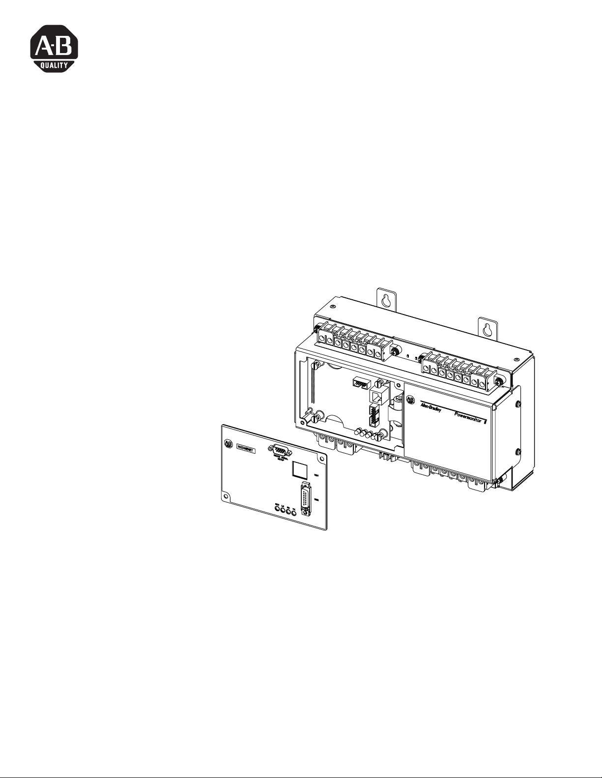
The Catalog Number 1403-NENET Ethernet Card is a
microprocessor-controlled, dual-port communication plug-in accessory to the
Po w ermonito r II Ma ster M odu le. This ac cesso ry provid es the Po wermon itor II
with three communication ports. Two of these ports are the 10BaseT and
10Base5 Ethe rnet ports, while the third is an RS-232 local configuratio n p ort.
Required configuration parameters (IP Address, Gateway, Subnet Mask,
Physical Ethernet Port, etc.) are provided by configuring the Master Module.
(There are no hardware jumpers to configure when the card is installed.)
Page 6
2 Product Description
Features
The Ethernet Communication Card features include:
• Connect to Allen-Bradley PLC-5
• Connect to Allen-Bradley SLC 5/05™ Ethernet processor
• Built-in in ternet web page support
• Compatible with RSEnergy™, RSView32™ and RSPower32™
®
Ethernet processors
software
• Ethernet communication rate: 10Mbps
• Comp atible w i th commercially available network bridges and routers
• Fully software configurable
• Sup ports RSLi nx™ and WINtelligent Linx™ (emulates SLC 500™)
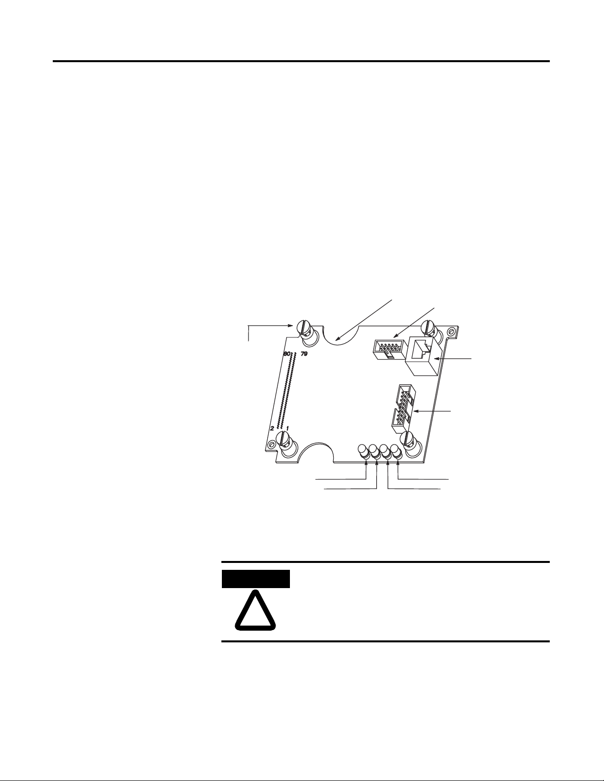
Figure 1 Catalog Number 1403-NENET Communications Module
Finger Hol d
Captive Fastening Screw
Internal RS-232 Connector
10BT Connector
Installation
Internal 10B5 Connector
Ready (RDY) L ED
Link (LK) LED
ATTENTION
Please follow appropriate ESD procedures before removal
and/or installation of the Ethernet Communications Card.
Receive (RX) L ED
Transmit (TX) LED
Failure to follow these procedures can result in physical
!
damage to both the Ethernet Communications Card and
the Master Module.
1. Remove Master Module control power .
2. Remove the blank plate by unscrewing the two corner retaining screws
as shown i nFigure 2. Save these two screws for assembly.
Publication 1403-IN005A-EN-P
Page 7
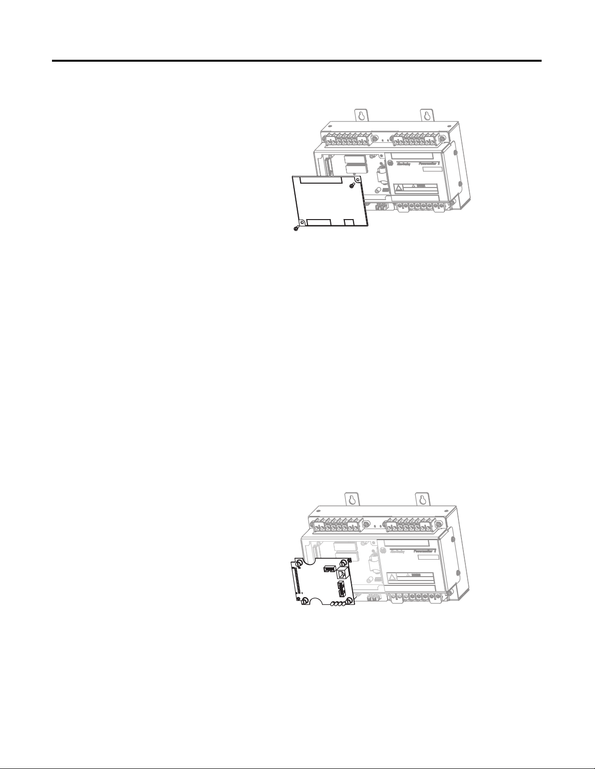
Product Description 3
Figure 2 Blank Plate Removal
3. If you plan to remove the communications card at a later date, retain the
blank plate. Otherwise, dispose of properly.
4. Remove the communications card from the static protection shipping
bag.
5. Grasp the card with the components side up and the four LEDs on the
bottom. Place the right index finger in the top notch and the thumb in
the bottom notch.
6. With the Master Module labels right side up, place the card into
opening on the left side, as shown in Figure 3. The card to Master
Module connector should align properly when the top right and bottom
left guide pins of the Master Module mate with holes in the card. With
your left thumb, press just above the card to Master Module connector
to attach the connector. Tighten the fo ur corner screws on the
communication card.
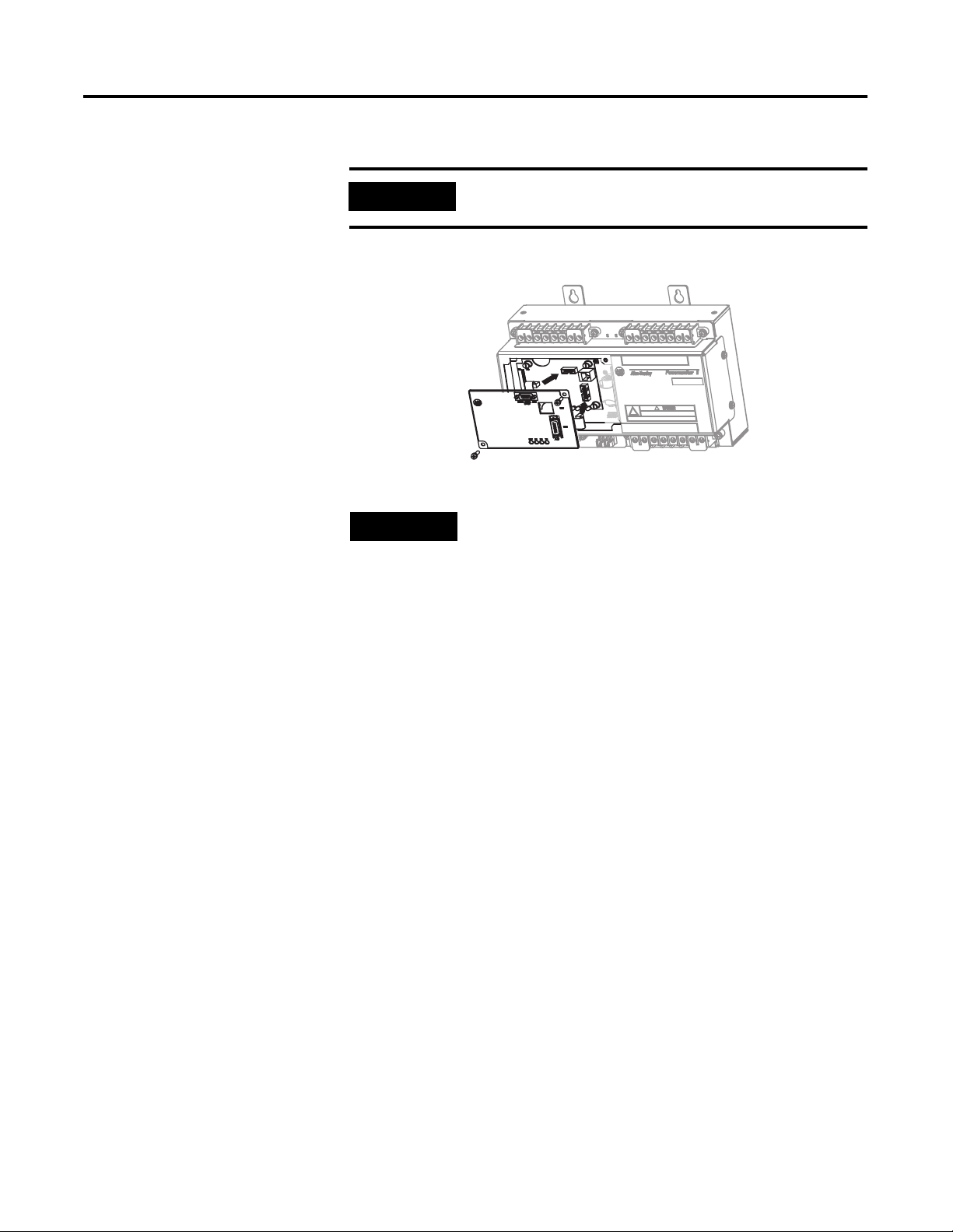
Figure 3 Installing Communication Card
7. Place the closure plate over the opening. Connect the closure plate
ribbon connectors to the communication card connectors. Secure it with
the t wo scre ws from the original blank plate as sh own inFig ure 4.
Publi cation 1403-IN005A-EN-P
Page 8
4 Product Description
Field Service Considerations
IMPORTANT
Figure 4 Installing Closure Plate
NOTE
8. Apply Master Module control power.
If the Ethernet Communications Card requires service, please contact your
nearest Rockwell Automation Sales Office. To minimize your inconvenience,
the initial installation shoul d be performed in a manner which makes removal
easy .
Make sure cables do not twist.
Refer to Appendix D on page D-1, for screw torque
requirements and wire sizes.
General Operation
Publication 1403-IN005A-EN-P
Communications Card Set-Up
All Ethernet card configuration items (Table 4 on page 6) can be changed via
the Display Module or via the RS-232 setup port on the Ethernet card . If using
a Display Module for Ethernet card configuration, all of the communication
configuration items can be found in the Display Module menu/parameter
structure unde r: Program
1403 Powermonitor II Instruction Sheet, Publication 1403-IN001A-US-P for
general information on Display M odule operation.)
The serial port on the 1403-NENET may be used to set communications
options as well. Follow these steps:
1. Connect to a PC using a standard RS-232 null modem cable.
2. Run a communication application (such as Hyper Terminal) on the PC.
3. Set the communications parameters. Se eTable 2 for communications
parameter settings.
➞ Configuration ➞ Communication. (Refer to
Page 9

Product Description 5
Table 2 Communication Parameters
Parameter Value
Baud Rate 38,400
Parity None
Data Bits 8
Stop Bits 1
Flow Control None
4. Apply control power to the Master Module.
5. Press Enter (or Return) on the PC.
6. Follow the on-screen instructions to modify and save the options.
Connections
There are two communication connection types for the 1403-NENET.
• UTP (10BaseT) - use a standard straight through RJ45 cable to connect
to an Ethernet hub.
• AUI - attach an Ethernet transceiver to the DB15 connector.
NOTE
The final installation should contain wiring to one port
only .
Publi cation 1403-IN005A-EN-P
Page 10

6 Product Description
Indicators
Four LED indicators provide information about the operating status of the
card.
Table 3 LED Indicators
Label Name LED Color LED State and Communications Condition
RDY Ready Red ON = Control power applied
ON/OFF Flashing = Self-test initialization
LK Link Green ON = UTP (10BaseT) cable properly connected
RX Receive Green ON/OFF Fl a shi n g = R eceiving Data
TX Transmit Green ON/OF F Flas h i ng = Tr an smitting D ata
Configuration Items
Table 4 Communication Configuration Items
Communication Parameter Description Range Default
IP Address Byte a IP address of this Powermonitor. (Normally in the form
IP Address Byte b 1
IP Address Byte c 1
IP Address Byte d Devi ce ID#
Subnet Mask Byte a Specifies the subnet mask to apply to the IP address.
Subnet Mask Byte b 255
Subnet Mask Byte c 255
Subnet Mask Byte d 0
Physical Ethernet Por t Selects the Etherne t medi a (0=UTP/1 0B a s eT, 1=AUI/
Keep Alive Time The maximum allowable time any socket is dedicated to a
Inactivity Time The maximum allowable time the entire Ethernet
128.1.1.1)
Network ID and Host are specified by address class. Zero
bits in the mask indicate bit positions of the host number;
one bits are for subnet ID. (Normally in the form
255.255.255.0)
10Base 5)
connection that is not respo nding.
communi cation ca rd waits with no network activity
befor e re booting.
Set parameter to zero to disable inactivity time.
Communication
0 to 255 128
0 to 255 255
0 = UTP, 1 =AUI 0 = UTP
5 to 3600 seconds 30
0 to 1440 minutes
0 = Disabled
30
Publication 1403-IN005A-EN-P
NOTE
BOOT P, the dynamic acquisition of an IP address, is
enabled when all four address bytes of the programmed IP
address are set to zero. (0.0.0.0)
Page 11

Product Description 7
1403-NENET Web Access Overview
The HTTP (Web) interface is accessed from a web browser by entering the IP
address of the Powermonitor II in the address combo box
(example: http://128.1.1.151).
A menu of all the available tables is presented with each table name shown as a
hyperlink. Clicking on the link brings up a tabular display of the values in that
table and the value descriptions.
Publi cation 1403-IN005A-EN-P
Page 12

8 Product Description
Publication 1403-IN005A-EN-P
Page 13
Communications Cards
Bulletin Number Type of Device
Catalog Number Explanation
1403 - NENET
Appendix
A
1403 = Powermonitor II Family of products. NENET = Plug-in Communication Card for Bulletin 1403-MM and 1403-LM
Devices (TCP/IP Ethernet).
1 Publi cation 1403-IN005A-EN-P
Page 14

A-2 Catalog Number Explanation
Publication 1403-IN005A-EN-P
Page 15

Table B.1 Data Table List
Appendix
Ethernet Communication Card Data Tables
B
Table Name Number of
Parameters
Device Configuration Data T able - Write and Read
(File N11)
Communications Configuration Table - Write and
Read (File N12)
Command Data Table Write (File N13) 12 N13/22 Write B-7
Voltage/Current Data - Read (File F14) 24 F14/29 Read B-9
Real- Time Power Data - Read (File F15) 25 F15/33 Read B-10
Cumulative Power Data - Read (File N16) 7 N16/45 Read B-11
Demand Data - Read (File F17) 18 F17/23 Read B-12
Event Log - Read (File N18) 12 N18/23 Read B-13
Snapshot 46 Parameter Record Table Read (File
F19)
Power Snapshot Log Data Table (File F20) 30 F20/34 Read B-20
Min_Max Log - Read (File N21) 8 N21/24 Read B-22
Log Selection Command Table Write (File N22) 4 N22/9 Write B-23
Even Harmonic Distortion Table - Channel 1 to 7
Read (File F23)
37 N11/44 Read/Write B-2
21 N12/30 Read/Write B-6
29 F19/32 Read B-14
29 F23/32 Read ( Channels 1 to 7) B-25
File/
Number of Elements
Type of Table Page
Odd Harm onic Distortion Table - Channels 1 to 7
Read (File F24)
Even Harmonic Magnitude Data Table Channel 1
to 7 Read (File F25)
Odd Harmonic Magnitude Data Table (File F26) 29 F26/30 Read (Channel 1 to 7) B-29
Even Harmonic Phase Angle Data Table Channels
1 to 7 Read (File F27)
Odd Harmonic Phase Angle Data Table (File F28) 29 F28/29 Read (Channel 1 to 7) B-32
Waveform Capture Data - Read (File N29) 54 N29/63 Read B-34
Diagnostic Data Table (Self-test Results) Read
(File N30)
Setpoint Setup Data Table - Write/Read (File N31) 9 N31/20 Read/Write B-39
Relay/Setpoint Statu s Table Read (File N32) 29 N3 2/38 Read B-41
Combined Real-Time Data T able Read (File F40) 81 F40/94 Read B-44
1 Publi cation 1403-IN005A-EN-P
29 F24/32 Read ( Channels 1 to 7) B-26
29 F25/31 Read (Channel 1 to 7) B-28
29 F27/30 Read (Channel 1 to 7) B-31
33 N30/39 Read B-37
Page 16

B-2 Ethernet Communication Card Data Tables
Table B.2 Device Configuration Data Table - Write and Read (File N11)
Parameter No. Parameter Name Master Module Range Default
Element Range
Setting
1.1 Voltage Mode 0 = Demo
41 0 to 5
1 = Single
2 = Open Delta
3 = 3-Wire Delta
4 = 4-Wire Wye
5 = Direct Delta
1.2 Present Unit Password -1 is always returned on a
(1)
0 2 -1 to +999 9
Read
0 to 9999 is required for a
Write
1.3 New Passwor d -1 does not chan ge the
0 3 -1 to +999 9
password
0 to 9999 is new password
value
1.4 Voltage Scale 1.0 to 10,000,000.0 120.0 4 0 to 9999
PT Primary 5 0 to 4
1.5 Voltage Scale 1 to 999 120 6 1 to 999
PT Seco nd ary
1.6 Current Scale (For I1,
1.0 to 10,000,000.0
1 or 5
(2)
7 0 to 9999
I2, I3)
CT Primary 8 0 to 4
1.7 Current Scale (For I1,
1 to 999
1 or 5
(2)
9 1 to 999
I2, I3)
CT Secondary
1.8 Analog Input Scale 1.0 to 10,000,000.0 1.0 10 0 to 9999
PT Primary 11 0 to 4
1.9 Analog Input Scale 1 to 999 1 12 1 to 999
PT Seco nd ary
1.10 Neutral Current Scale
1.0 to 10,000,000.0
1 or 5
(2)
13 0 to 9999
(For I4)
CT Primary 14 0 to 4
1.11 Neutral Current Scale
1 to 999
1 or 5
(2)
15 1 to 999
(For I4)
CT Secondary
1.12 Demand Period Length -99 to +99 1 16 -99 to +99
1.13 Number of Demand
1 to 15 1 17 1 to 15
Periods
1.14
Snapshot Log Type
(3)
0 = 46 param record
018 0 to 5
1 = 16 param record
2 = 8 param record
3 = 4 param record
4 = 3 and 7 param record
5 = 1 param record
Publication 1403-IN005A-EN-P
Page 17

Table B.2 Device Configuration Data Table - Write and Read (File N11)
Ethernet Communication Card Data Tables B-3
Parameter No. Parameter Name Master Module Range Default
Setting
1.15 Snapshot Interval -
0 19 0 to 32,767
Hours
1.16 Snapshot Interval -
0 20 0 to 32,767
Minutes
1.17 Snapshot Interval -
0 21 0 to 32,767
Seconds
1.18 Snapshot Buffer Type 0 = Fill and Stop
122 0 to 1
1 = Circular
(3)
1.19
1.20
1.21
1.22
Snaps ho t Param #1
Snaps ho t Param #2
Snaps ho t Param #3
Oscillograph Type
SeeTable B.3 62 23 0 to 64
(3)
SeeTable B.3 63 24 0 to 64
(3)
SeeTable B.3 47 25 0 to 64
(3)
0 = V2.10 or earlier
026 0 to 6
compatible mode
1 = 1 0 .8 kHz, 1 capture
2 = 1 0 .8 kHz, 2 captures
3 = 5.4 kH z, 1 capture
4 = 5.4 kH z, 2 captures
5 = 2.7 kH z, 1 capture
6 = 2.7 kH z, 2 captures
1.23 Oscillograph
Overwr i t e Timeou t
1.24 Output Pulse Relay
No.
1 to 4320 minutes 1 27 1 to 4320
(3)
0 = None
028 0 to 2
1 = Relay 1
2 = Relay 2
1.25 O utput Pulse
Parameter
0 = kWh Forward
1 = kWh Reverse
029 0 to 3
2 = kVarh Forward
3 = kVarh Reverse
1.26 O utput Pulse
1 to 32766 1 30 1 to 32766
Increment
1.27 Outp u t Puls e Width
(4)
(ms)
1.28 Ch A 12 Cycle
Oscillogram
(5)
0, 40 to 2000 100 31 40 to 2000
1 = Phase 1 Voltage
132 1 to 7
2 = Phase 1 Current
3 = Phase 2 Voltage
4 = Phase 2 Current
5 = Phase 3 Voltage
6 = Phase 3 Current
7 = Phase 4 Current
1.29 Ch B 12 Cycle
Oscillogram
(5)
1 = Phase 1 Voltage
2 = Phase 1 Current
233 1 to 7
3 = Phase 2 Voltage
4 = Phase 2 Current
5 = Phase 3 Voltage
6 = Phase 3 Current
7 = Phase 4 Current
Element Range
Publi cation 1403-IN005A-EN-P
Page 18

B-4 Ethernet Communication Card Data Tables
Table B.2 Device Configuration Data Table - Write and Read (File N11)
Parameter No. Parameter Name Master Module Range Default
Setting
1.30 Oscillograph Buffer
(5)
Type
1.31 Number of Pretrigger
Cycles for the 12 Cycle
Oscillogram
(5)
1.32 IEEE 519 Max. Short
Circuit Current
(5)
1.33 IEEE 519 Max.
0 = Hold
134 0 to 1
1 = Overwrite
-1 = No Pret rig
0 35 -1 to +8
0 to +8 = Cycles
0.0 to 10,000,000.0 0 36 0 to 9999
0.0 to 10,000,000.0 0 38 0 to 9999
Demand/Load
(5)
Current
1.34 Save Status Changes
to Event Log
1.35 Vaux Voltage Mode 0 = AC
0 = No
1 = Yes
040 0 to 1
041 0 to 1
1 = DC
1.36 Filter Mo de (14 03 -MM)
Enable THD (1403- LM)
1.37 Enable Min_Max Log 0 = No
1 to 3 (1403-MM)
0 to 1 (1403-LM)
2 (1403-MM)
0 (1403-LM)
143 0 to 1
1 = Yes
Reserved 44
Element Range
37 0 to 4
39 0 to 4
42 1 to 3 (1403-MM)
0 to 1 (1403-LM)
(1) Available on 1403-MM firmware V2.0 o r later and 1403-LM firmware V1.01 or later.
(2) This va l ue is 1 for 1-Amp Ma ster Module (Cat. No. 1403-MM01X) or 5 for a 5-Amp Master Module (Cat. No. 1403-MM05X).
(3) Available on firmware V 3 .00 or later (reserved in previous versions).
(4) For transitional KYZ pulse enter 0.
(5) 1403-MM only , not available on 1403-LM version.
Publication 1403-IN005A-EN-P
Page 19

Ethernet Communication Card Data Tables B-5
Table B.3 Configurable Snapshot Parameter List (selection list for Table B.2, parameters 1.19, 1.20 and 1.21)
Parameter Number Parameter Name Parameter Number Parameter Name
0 L1 Cu rrent 33 Total A pparent Power
1 L2 Current 34 L 1 True PF
2 L3 Current 35 L 2 True PF
3 Avg Current 36 L3 T rue PF
4 L4 Cu rrent 37 Total True PF
5 L1-N Voltage 38 L1 Displacement PF
6 L2-N Voltage 39 L2 Displacement PF
7 L3-N Voltage 40 L3 Displacement PF
8 Avg L-N Voltage 41 Total D is p l a c em e nt PF
9 L1-L2 Voltag e 42 L1 Distort ion PF
10 L2-L3 Voltage 43 L2 Dis t ortion PF
11 L3-L1 Voltage 44 L3 Dis t ortion PF
12 Avg L-L Voltage 45 Total Distortion PF
13 Frequency 46 Demand I
14 Pos Seq Current 47 Demand W
15 Neg Seq Current 48 Demand VAR
16 Current Unbalance 49 Demand VA
17 Pos Seq Voltage 50 Proj #1 Demand I
18 Neg Seq Voltage 51 Proj #1 Demand W
19 Voltage Unbalance 52 Proj #1 Demand VAR
20 Aux Voltage 53 Proj #1 Demand VA
21 Aux Frequency 54 Proj #2 De m and I
22 L1 Real Power 55 Proj #2 Demand W
23 L2 Real Power 56 Proj #2 Demand VAR
24 L3 Real Power 57 Proj #2 Demand VA
25 Total R eal Powe r 58 Proj #3 Demand I
26 L1 Reactive Power 59 Pro j # 3 D emand W
27 L2 Reactive Power 60 Pro j # 3 D emand VAR
28 L3 Reactive Power 61 Pro j # 3 D emand VA
29 Total R eactive Power 62 KWh net
30 L1 Apparent Power 63 KVARh net
31 L2 Apparent Power 64 KVAh net
32 L3 Apparent Power
Publi cation 1403-IN005A-EN-P
Page 20

B-6 Ethernet Communication Card Data Tables
NOTE
Table B.4 Communications Configuration Table - Write and Read (File N12)
Parameter
No.
2.1 IP Address Byte a 0 to 255 128 1 0 to 255
2.2 IP Address Byte b 0 to 255 1 2 0 to 255
2.3 IP Address Byte c 0 to 255 1 3 0 to 255
2.4 IP Address By te d 0 to 255 Unit ID 4 0 to 255
2.5 Reserved 0 0 5 0
2.6 Reserved 0 0 6 0
2.7 Reserved 0 0 7 0
2.8 Reserved 0 0 8 0
2.9 Subnet Mask Byte a 0 to 255 255 9 0 to 255
2.10 Subnet Mask Byte b 0 to 255 255 10 0 to 255
2.11 Subnet Mask Byte c 0 to 255 255 11 0 to 255
2.12 Subnet Mask Byte d 0 to 255 0 12 0 to 255
2.13 Physical Ethernet Port 0 = UTP, 1 = AUI 0 13 0 to 1
2.14 Keep Alive Time 5 to 3600 Seconds 30 14 5 to 3600
2.15 Inactivity Time 0 to 1440 Minutes 30 15 0 to 1440
2.16 Reserved 0 0 16 0
2.17 Reserved 0 0 17 0
2.18 Reserved 0 0 18 0
2.19 Reserved 0 0 19 0
2.20 Reserved 0 0 20 0
2.21 Present Unit Password -1 is always returned for
Parameter Name Master Module Range Default Element Range
a Read
0 to 9999 is re qu i red for a
Write
Reserved 0 0 22 0
Reserved 0 0 23 0
Reserved 0 0 24 0
Reserved 0 0 25 0
Reserved 0 0 26 0
Reserved 0 0 27 0
Reserved 0 0 28 0
Reserved 0 0 29 0
Reserved 0 0 30 0
The device does not respond to a broadcast of this table. IP
addresses are stored as a.b.c.d (e.g. 128.1.1.1; a=128).
-1 (Rea d) 21 -1 to +9999
Publication 1403-IN005A-EN-P
Page 21

Ethernet Communication Card Data Tables B-7
Table B.5 Command Data Table Write (File N13)
Parameter No. Parameter Name Master Module Range Element Range
3.1 Command Word 1 (Bit Fields) SeeTable B.6 1 0 to 32,767
3.2 Command Word 2 (Bit Fields) SeeTable B.7 2 0 to 511
3.3
Harmonic Analysis
(1)
1 = L1 Voltage
31 to 7
2 = L1 Current
3 = L2 Voltage
4 = L2 Current
5 = L3 Voltage
6 = L3 Current
7 = L4 Current
3.4 Oscill ograph Channel Request
(Not Av ailable on 1403-LM)
1 = Capture #1 V1
2 = Capture #1 I1
4 1 to 17
3 = Capture #1 V2
4 = Capture #1 I2
5 = Capture #1 V3
6 = Capture #1 I3
7 = Capture #1 I4
8 = Ch-A 12 Cycle
9 = Ch-B 12 Cycle
10 = Reser v ed
(2)
(2)
(2)
(2)
(2)
(2)
(2)
5 - 9999 to 999 9
6
8
7 - 9999 to 999 9
8
±0 to 8
±0 to 8
3.5 W Hour Data for Set Command
3.6 VAR Hour Data for Set Command
11 = Capture #2 V1
12 = Capture #2 I1
13 = Capture #2 V2
14 = Capture #2 I2
15 = Capture #2 V3
16 = Capture #2 I3
17 = Capture #2 I4
-9999x10
-9999x10
8
to +9999x108
8
to +9999x10
3.7 Reserved 9
10
3.8 Time for Set Command Year 11 1998 to 2097
Month, Day 12 8-bit, 8-bi t
Hour, Minutes 13 8-bit, 8-bit
Seconds, Hundredths 14 8-bit, 8-bit
3.9 Force Specifics Relay 1 1 = Energize
15 1, 2, 4
2 = De-energ ize
4 = Remove Fo r ce
3.10 Force Specifics Relay 2 1 = Energize
16 1, 2, 4
2 = De-energ ize
4 = Remove Fo r ce
3.11 Setpoint Number 1 to 20 17 1 to 20
Publi cation 1403-IN005A-EN-P
Page 22

B-8 Ethernet Communication Card Data Tables
Table B.5 Command Data Table Write (File N13)
Parameter No. Parameter Name Master Module Range Element Range
3.12 Present Unit Password 0 to 9999 18 0 to 9999
Reserved 19
Reserved 20
Reserved 21
Reserved 22
(1) S ee Tabl e B.6 o n pageB-8 for specific command bi ts to enable these features.
(2) Available on firmware V3.00 or later.
Table B.6 Bit Fields for Command Data Table -(Command Word 1)
Command Bit Location and
Value
Clear Snapshot Log b0 = 1
Clear Min_Max Log b1 = 1
Restore Factory Default Configuration b2 = 1
Clear Hold of Oscillog raph Capt ure #1 (Reserv ed on 1403 - LM) b3 = 1
Initiate Oscillograph Capture #1 (Reserved on 1403-LM) b4 = 1
Force Self Test b5 = 1
Clear Status Input Counter 1 b6 = 1
Clear Status Input Counter 2 b7 = 1
Clear Status Input Counter 3 b8 = 1
Clear Status Input Counter 4 b9 = 1
Clear Battery Usage Timer b10 = 1
Reserved b11 = 1
Synchronize Demand Interval b12 = 1
Clear Hold of Oscil l ograph Capture #2 (R es erved on 1403-LM) b13 = 1
Initiate Oscillograph Capture #2 (Reserved on 1403-LM) b14 = 1
Table B.7 Bit Fields for Command Data Table - (Command Word 2)
Command Bit Location and
Value
Publication 1403-IN005A-EN-P
Set Analysis Channel Request (DV1) b0 = 1
Set Oscillogram Channel Request (DV2)
b1 = 1
(Not Available on 1403-LM)
Set W Hours (DV3) b2 = 1
Set VAR Hours (DV4) b3 = 1
Page 23

Ethernet Communication Card Data Tables B-9
Table B.7 Bit Fields for Command Data Table - (Command Word 2)
Command Bit Location and
Value
Reserved b4 = not used
Set Time (DV6) b5 = 1
Relay 1 (DV7) b6 = 1
Relay 2 (DV8) b7 = 1
Select Setpoint Number ( D V9) b8 = 1
Table B.8 Voltage/Current Data - Read (File F14)
Parameter No. Parameter Name Master Module Range Element Range
4.1 Time Stamp Year 1 32-bit Float
Month, Date 2 32-bit Float
Hour, Minute 3 32-bit Float
Seconds, Hundredths 4 32-bit Float
4.2 L1 Current
4.3 L2 Current
4.4 L3 Current
4.5 L4 (Neutral) Current
4.6 3-Phase Average Current
4.7 Positive Sequence Current
4.8 Negative Sequence Current
0 to 9999x10
0 to 9999x10
0 to 9999x10
0 to 9999x10
0 to 9999x10
0 to 9999x10
0 to 9999x10
21
21
21
21
21
21
21
amps
amps
amps
amps
amps
amps
amps
5
6
7
8
9
10
11
0 to 9999x10
0 to 9999x10
0 to 9999x10
0 to 9999x10
0 to 9999x10
0 to 9999x10
0 to 9999x10
21
21
21
21
21
21
21
4.9 Percent Current Unbalance 0.0 to 100.0 12 0.0 to 100.0
4.10 L1 to L2 Voltage
4.11 L2 to L3 Voltage
4.12 L3 to L1 Voltage
4.13 AUX Voltage
4.14 3-Phase Average Voltage (L-L)
4.15 Positive Sequence Voltage
4.16 Negative Sequence Voltage
0 to 9999x10
0 to 9999x10
0 to 9999x10
0 to 9999x10
0 to 9999x10
0 to 9999x10
0 to 9999x10
21
21
21
21
21
21
21
amps
volts
amps
volts
amps
volts
volts
13
14
15
16
17
18
19
0 to 9999x10
0 to 9999x10
0 to 9999x10
0 to 9999x10
0 to 9999x10
0 to 9999x10
0 to 9999x10
4.17 Percent Voltage Unbalance 0.0 to 100.0 20 0.0 to 100.0
4.18 L1-N Voltage
4.19 L2-N Voltage
4.20 L3-N Voltage
4.21 3-Phase Average Voltage (L-N)
0 to 9999x10
0 to 9999x10
0 to 9999x10
0 to 9999x10
21
21
21
21
volts
volts
volts
volts
21
22
23
24
0 to 9999x10
0 to 9999x10
0 to 9999x10
0 to 9999x10
Publi cation 1403-IN005A-EN-P
21
21
21
21
21
21
21
21
21
21
21
Page 24

B-10 Ethernet Communication Card Data Tables
Table B.8 Voltage/Current Data - Read (File F14)
Parameter No. Parameter Name Master Module Range Element Range
4.22 Reserv ed Word 25
4.23 Last Cycle Frequency 20.0 to 132.0 26 0 to 9999
4.24 Phase Rotation 0 = No Rotation
27 0 to 2
1 = ABC
2 = ACB
Reserved Word 28
Reserved Word 29
Table B.9 Real-Time Power Data - Read (File F15)
Parameter No. Parameter Name Master Module Range Element Range
5.1 Time Stamp Year 1 32-bit Float
Month, Date 2 32-bit Float
Hour, Minute 3 32-bit Float
Seconds, Hundredths 4 32-bit Float
5.2 L1 Real Power
5.3 L2 Real Power
5.4 L3 Real Power
5.5 Total Real Power
5.6 L1 Reactive Power
5.7 L2 Reactive Power
5.8 L3 Reactive Power
5.9 Total Rea ctive Power
5.10 L1 App ar ent Power
5.11 L2 App ar ent Power
5.12 L3 App ar ent Power
5.13 Total Apparent Power
0 to 9999x10
0 to 9999x10
0 to 9999x10
0 to 9999x10
0 to 9999x10
0 to 9999x10
0 to 9999x10
0 to 9999x10
0 to 9999x10
0 to 9999x10
0 to 9999x10
0 to 9999x10
21
21
21
21
21
21
21
21
21
21
21
21
W
W
W
W
VAR
VAR
VAR
VAR
VA
VA
VA
VA
5
6
7
8
9
10
11
12
13
14
15
16
0 to 9999x1021
0 to 9999x1021
0 to 9999x1021
0 to 9999x1021
0 to 9999x1021
0 to 9999x1021
0 to 9999x1021
0 to 9999x1021
0 to 9999x1021
0 to 9999x1021
0 to 9999x1021
0 to 9999x1021
5.14 L1 True PF -100.0 to +100.0 17 -100.0 to +10 0. 0
5.15 L2 True PF -100.0 to +100.0 18 -100.0 to +10 0. 0
5.16 L3 True PF -100.0 to +100.0 19 -100.0 to +10 0. 0
5.17 Total True PF -100.0 to +100.0 20 -100.0 to +100.0
5.18
5.19
5.20
5.21
Publication 1403-IN005A-EN-P
L1 Displa cement PF
L2 Displa cement PF
L3 Displa cement PF
(1)
(1)
(1)
Total Displ acement PF
-100.0 to +100.0 21 -100.0 to +100.0
-100.0 to +100.0 22 -100.0 to +100.0
-100.0 to +100.0 23 -100.0 to +100.0
(1)
-100.0 to +100.0 24 -100.0 to +100.0
Page 25

Ethernet Communication Card Data Tables B-11
Table B.9 Real-Time Power Data - Read (File F15)
Parameter No. Parameter Name Master Module Range Element Range
5.22
5.23
5.24
5.25
L1 Distortion PF
L2 Distortion PF
L3 Distortion PF
T otal Di stortion PF
(1)
(1)
(1)
(1)
-100.0 to +100.0 25 -100.0 to +100.0
-100.0 to +100.0 26 -100.0 to +100.0
-100.0 to +100.0 27 -100.0 to +100.0
-100.0 to +100.0 28 -100.0 to +100.0
Reserved Word 29
(1) This value has the same update rate as harmonic analysis.
Table B.10 Cumulative Power Data - Read (File N16)
Parameter No. Parameter Name Master Module
Element Range Modulus
Range
6.1 Time Stamp Year 1 N/A
Month, D a te 2 N/A
Hour, Minute 3 N/A
Seconds,
4N/A
Hundredths
6.2 kW Hours Forward
6.3 kW Hours Reverse
6.4 kW Hours Net
0 to 1.0x10
-1.0x10
-1.0x10
1.0x10
12
12
to 0
12
to
12
5 +0 to 999
6 +0 to 999
7 +0 to 999
8 +0 to 999
9 +0 to 999
10 -0 to 999
11 -0 to 999
12 -0 to 999
13 -0 to 999
14 -0 to 999
15 ±0 to 999
16 ±0 to 999
17 ±0 to 999
18 ±0 to 999
19 ±0 to 999
10
10
10
10
10
10
10
10
10
10
10
10
10
10
10
0
3
6
9
12
0
3
6
9
12
0
3
6
9
12
Publi cation 1403-IN005A-EN-P
Page 26

B-12 Ethernet Communication Card Data Tables
Table B.10 Cumulative Power Data - Read (File N16)
Parameter No. Parameter Name Master Module
Range
6.5 kVAR Hours Forward
6.6 kVAR Hours Reverse
6.7 kVAR Hours Net
0 to 1.0x10
-1.0x10
-1.0x10
1.0x10
12
12
to 0
12
to
12
Reser v ed Word 35
Reser v ed Word 36
Reser v ed Word 37
Reser v ed Word 38
Reser v ed Word 39
Reser v ed Word 40
Reser v ed Word 41
Reser v ed Word 42
Reser v ed Word 43
Reser v ed Word 44
Reser v ed Word 45
Element Range Modulus
20 +0 to 999
21 +0 to 999
22 +0 to 999
23 +0 to 999
24 +0 to 999
25 -0 to 999
26 -0 to 999
27 -0 to 999
28 -0 to 999
29 -0 to 999
30 ±0 to 999
31 ±0 to 999
32 ±0 to 999
33 ±0 to 999
34 ±0 to 999
10
10
10
10
10
10
10
10
10
10
10
10
10
10
10
0
3
6
9
12
0
3
6
9
12
0
3
6
9
12
Table B.11 Demand Data - Read (File F17)
Parameter No. Parameter Name Master Module Range Element Range
7.1 Time Stamp Year 1 32-bit Float
Month, Date 2 32-bit Float
Hour, Minute 3 32-bit Float
Seconds, Hundredths 4 32-bit Float
7.2 Demand Current
Publication 1403-IN005A-EN-P
0 to 9999x10
21
amps
5
0 to 9999x10
21
Page 27

Ethernet Communication Card Data Tables B-13
Table B.11 Demand Data - Read (File F17)
Parameter No. Parameter Name Master Module Range Element Range
7.3 Demand Power
7.4 Demand Reactive Power
7.5 Demand Ap pa rent Power
7.6 Projected No. 1 Demand Current
7.7 Projected No. 1 Dema nd Power
7.8 Projected No. 1 Demand Reactive Power
7.9 Projected No. 1 Demand Apparent Power
7.10 Projected No. 2 Demand Current
7.11 Projected No. 2 Dema nd Power
7.12 Projected No. 2 Demand Reactive Power
7.13 Projected No. 2 Dema nd Apparent Power
7.14 Projected No. 3 Demand Current
7.15 Projected No. 3 Dema nd Power
7.16 Projected No. 3 Demand Reactive Power
7.17 Projected No. 3 Dema nd Apparent Power
7.18 Elap s ed Time
0 to 9999x10
0 to 9999x10
0 to 9999x10
0 to 9999x10
0 to 9999x10
0 to 9999x10
0 to 9999x10
0 to 9999x10
0 to 9999x10
0 to 9999x10
0 to 9999x10
0 to 9999x10
0 to 9999x10
0 to 9999x10
0 to 9999x10
0 to 9999x10
21
21
21
21
21
21
21
21
21
21
21
21
21
21
21
21
W
VAR
VA
amps
W
VAR
VA
amps
W
VAR
VA
amps
W
VAR
VA
6
7
8
9
10
11
12
13
14
15
16
17
18
19
20
21
0 to 9999x10
0 to 9999x10
0 to 9999x10
0 to 9999x10
0 to 9999x10
0 to 9999x10
0 to 9999x10
0 to 9999x10
0 to 9999x10
0 to 9999x10
0 to 9999x10
0 to 9999x10
0 to 9999x10
0 to 9999x10
0 to 9999x10
0 to 9999x10
Reserved Word 22
Reserved Word 23
21
21
21
21
21
21
21
21
21
21
21
21
21
21
21
21
Table B.12 Event Log - Read (File N18)
(1)
Parameter No. Parameter Name Master Module Range Element Range
8.1 Event Time Log Stamp Year 1 16 Bit Integer
Month, Date 2 8-bit, 8-bit
Hour, Minute 3 8-bit, 8-bit
Seconds, Hundredths 4 8-bit, 8-bit
8.2 Event Type Value 0 to 14 5 0 to 14
8.3 Event Code Value 0 to 10 6 0 to 10
8.4 Setpoint Type 0 to 54 7 0 to 54
8.5 Setpoint Evaluation Condition 0 to 5 8 0 to 5
8.6 Setpoint Level
±9999x10
21
9 ±0 to 9999
10
±0 to 21
8.7 Setpoint Action/Release Delay 0 to 9999 11 0 to 9999
8.8 Setpoint Action 0 to 20 12 0 to 20
8.9 Number of Event Logs Requested 1 to 100 13 1 to 100
8.10 Number of Event Log Received (Counter) 1 to 100 14 1 to 100
Publi cation 1403-IN005A-EN-P
Page 28

B-14 Ethernet Communication Card Data Tables
Table B.12 Event Log - Read (File N18)
(1)
Parameter No. Parameter Name Master Module Range Element Range
8.11 Number of Event Log Being Returned 1 to 100 15 1 to 100
8.12 Internal Identifier -32767 to +32767 16 -32767 to +32767
Reserved Word 17
Reserved Word 18
Reserved Word 19
Reserved Word 20
Reserved Word 21
Reserved Word 22
Reserved Word 23
(1) ID=23 for log selection command.
Table B.13 Snapshot 46 Parameter Record Table Read (File F19)
Parameter No. Parameter Name Master Module
(1)
Element Range
Parameter Range
9.1 Timestamp of Snapshot Record Year 1 32-bit Float
Month, Date 2 32-bit Float
Hour, Minute 3 32-bit Float
Seconds, Hundredths 4 32-bit Float
9.2 Reserved 5
9.3 L1 Current
9.4 L2 Current
9.5 L3 Current
9.6 L4 (Neutral) Current
9.7 3-Phase Average Current
9.8 Positive Sequence Current
9.9 Negative Sequence Current
0 to 9999x10
0 to 9999x10
0 to 9999x10
0 to 9999x10
0 to 9999x10
0 to 9999x10
0 to 9999x10
21
21
21
21
21
21
21
amps
amps
amps
amps
amps
amps
amps
6
7
8
9
10
11
12
0 to 9999x10
0 to 9999x10
0 to 9999x10
0 to 9999x10
0 to 9999x10
0 to 9999x10
0 to 9999x10
21
21
21
21
21
21
21
9.10 Percent Current Unbalance 0.0 to 100.0 13 0.0 to 100.0
9.11 L1-L2 Voltage
9.12 L2-L3 Voltage
9.13 L3-L1 Voltage
9.14 AUX Voltage
9.15 3-Phase Average Voltage (L-L)
9.16 Positiv e S equence Voltage
9.17 Negative Sequence Voltage
0 to 9999x10
0 to 9999x10
0 to 9999x10
0 to 9999x10
0 to 9999x10
0 to 9999x10
0 to 9999x10
21
21
21
21
21
21
21
volts
volts
volts
volts
volts
volts
volts
14
15
16
17
18
19
20
0 to 9999x10
0 to 9999x10
0 to 9999x10
0 to 9999x10
0 to 9999x10
0 to 9999x10
0 to 9999x10
21
21
21
21
21
21
21
9.18 Percent Voltage Unbalance 0.0 to 100.0 21 0.0 to 100.0
9.19 L1-N Voltage
9.20 L2-N Voltage
0 to 9999x10
0 to 9999x10
21
21
volts
volts
22
23
0 to 9999x10
0 to 9999x10
21
21
Publication 1403-IN005A-EN-P
Page 29

Ethernet Communication Card Data Tables B-15
Table B.13 Snapshot 46 Parameter Record Table Read (File F19)
Parameter No. Parameter Name Master Module
(1)
Element Range
Parameter Range
9.21 L3-N Voltage
9.22 3-Phase Average Voltage (L-N)
0 to 9999x10
0 to 9999x10
21
21
volts
volts
24
25
0 to 9999x10
0 to 9999x10
21
21
9.23 Reserved 26
9.24 Last Cycle Frequency 20.0 to 132.0 27 20.0 to 132.0
9.25 Phase Rotation 0 = No Rotation
28 0 to 2
1 = ABC
2 = ACB
9.26 Number of Snapshot Logs Requested 1 to 50 29 1 to 50
9.27 No. of Snapshot Log Received (Counter) 1 to 50 30 1 to 50
9.28 Number of Snapshot Log Being Returned 1 to 50 31 1 to 50
9.29 Internal Identifier -32767 to +32767 32 -32767 to +32767
(1) ID=54 for log selection command.
Table B.14 Snapshot 16 Parameter Record Table Read (File F19)
Parameter No. Parameter Name Master Module Parameter Range Element
9a.1 Timestamp; Year 1998 to 2097 1
Timestamp; Month, Date 257 to 3103
Month = Value/256
Date = Remainder of Value/256
Timestamp; Hour, Minute 0 to 5947
Hour = Value/256
Minute = Remainder of Value/256
Timestamp; Seconds, Hundreths 0 to 15203
Seconds = Value/256
hSeconds = Remainder of Value/256
9a.2 Reserved 0 5
9a.3 L1-L2 Voltage (in Delta modes) or
0 to 9999x10
21
Volts
L1-N Voltage (in non-Delta modes)
9a.4 L2-L3 Voltage (in Delta modes) or
0 to 9999x10
21
Volts
L2-N Voltage (in non-Delta modes)
9a.5 L3-L1 Voltage (in Delta modes) or
0 to 9999x10
21
Volts
L3-N Voltage (in non-Delta modes)
9a.6 L1 Current
9a.7 L2 Current
9a.8 L3 Current
9a.9 L4 Current
0 to 9999x10
0 to 9999x10
0 to 9999x10
0 to 9999x10
21
Amps
21
Amps
21
Amps
21
Amps
9a.10 Voltage Unbalance 0 to 100% 13
9a.11 Current Unbalance 0 to 100% 14
9a.12 Tota l Real Pow er
9a.13 Total Reactive Power
9a.14 Demand kW
0 to 9999x10
0 to 9999x10
0 to 9999x10
21
21
21
kW
kVAR
kW
2
3
4
6
7
8
9
10
11
12
15
16
17
Publi cation 1403-IN005A-EN-P
Page 30

B-16 Ethernet Communication Card Data Tables
Table B.14 Snapshot 16 Parameter Record Table Read (File F19)
Parameter No. Parameter Name Master Module Parameter Range Element
9a.15 Demand kV A R
0 to 9999x10
21
kVAR
9a.16 Total True PF -100 to +100 19
9a.17 kWh net
9a.18 kVARh net
-9999x10
-9999x10
21
to +9999x1021 kWh
21
to +9999x1021 kVARh
9a.19 Number of Records Requested 1 to 265 22
9a.20 Number of Records Read so far 1 to 265 23
9a.21 Record Number Returned 1 to 265 24
9a.22 Internal Identifier 0 to 255 25
9a.23 Reserved 0 26
9a.24 Reserved 0 27
9a.25 Reserved 0 28
9a.26 Reserved 0 29
9a.27 Reserved 0 30
9a.28 Reserved 0 31
9a.29 Reserved 0 32
18
20
21
Table B.15 Snapshot 8 Parameter Record Table Read (File F19)
Parameter No. Parameter Name Master Module Parameter Range Element
9b.1 Timestamp; Year 1998 to 2097 1
Timestamp; Month, Date 257 to 3103
Month = Value/256
Date = Remainder of Value/256
Timestamp; Hour, Minute 0 to 5947
Hour = Value/256
Minute = Remainder of Value/256
Timestamp; Seconds, Hundreths 0 to 15203
Seconds = Value/256
hSeconds = Remainder of Value/256
9b.2 Reserved 0 5
9b.3 Avg L-L Voltage (in Delta modes) or Avg L-N
0 to 9999x10
21
Volts
Voltage (i n non-De l ta modes)
9b.4 Averag e C ur rent
0 to 9999x10
21
Amps
9b.5 Total True PF -100 to +100 8
9b.6 Total Real Power
0 to 9999x10
21
kW
9b.7 Frequency 0 to 75 Hz 10
9b.8 Voltage Unbalance 0 to 100% 11
9b.9 Current Unbalance 0 to 100% 12
9b.10 Total Reacti v e Po we r
0 to 9999x10
21
kVAR
9b.11 Number of Records Requested 1 to 489 14
9b.12 Number of Records Read so far 1 to 489 15
9b.13 Record Number Returned 1 to 489 16
9b.14 Internal Identifier 0 to 255 17
2
3
4
6
7
9
13
Publication 1403-IN005A-EN-P
Page 31

Ethernet Communication Card Data Tables B-17
Table B.15 Snapshot 8 Parameter Record Table Read (File F19)
Parameter No. Parameter Name Master Module Parameter Range Element
9b.15 Reserved 0 18
9b.16 Reserved 0 19
9b.17 Reserved 0 20
9b.18 Reserved 0 21
9b.19 Reserved 0 22
9b.20 Reserved 0 23
9b.21 Reserved 0 24
9b.22 Reserved 0 25
9b.23 Reserved 0 26
9b.24 Reserved 0 27
9b.25 Reserved 0 28
9b.26 Reserved 0 29
9b.27 Reserved 0 30
9b.28 Reserved 0 31
9b.29 Reserved 0 32
Table B.16 Snapshot 4 Parameter Record Table Read (File F19)
Parameter No. Parameter Name Master Module Parameter Range Element
9c.1 Timestamp; Year 1998 to 2097 1
Timestamp; Month, Date 257 to 3103
Month = Value/256
Date = Remainder of Value/256
Timestamp; Hour, Minute 0 to 5947
Hour = Value/256
Minute = Remainder of Value/256
Timestamp; Seconds, Hundreths 0 to 15203
Seconds = Value/256
hSeconds = Remainder of Value/256
9c.2 Reserved 0 5
9c.3 Avg L-L Voltage (in Dealt modes) or Avg L-N
0 to 9999x10
21
Volts
Voltage (i n non-De l ta modes)
9c.4 Aver age Current
0 to 9999x10
21
Amps
9c.5 Total True PF -100 to +100 8
9c.6 To tal Real Power
0 to 9999x10
21
kW
9c.7 Number of Records Re quested 1 to 846 10
9c.8 Number of Records Read so far 1 to 846 11
9c.9 Record Number Returned 1 to 846 12
9c.10 Internal Identifier 0 to 255 13
9c.11 Reserved 0 14
9c.12 Reserved 0 15
9c.13 Reserved 0 16
9c.14 Reserved 0 17
9c.15 Reserved 0 18
2
3
4
6
7
9
Publi cation 1403-IN005A-EN-P
Page 32

B-18 Ethernet Communication Card Data Tables
Table B.16 Snapshot 4 Parameter Record Table Read (File F19)
Parameter No. Parameter Name Master Module Parameter Range Element
9c.16 Reserved 0 19
9c.17 Reserved 0 20
9c.18 Reserved 0 21
9c.19 Reserved 0 22
9c.20 Reserved 0 23
9c.21 Reserved 0 24
9c.22 Reserved 0 25
9c.23 Reserved 0 26
9c.24 Reserved 0 27
9c.25 Reserved 0 28
9c.26 Reserved 0 29
9c.27 Reserved 0 30
9c.28 Reserved 0 31
9c.29 Reserved 0 32
Table B.17 Snapshot 3 and 7 Parameter Record Table Read (File F19)
Parameter No. Parameter Name Master Module Parameter Range Element
9d.1 Timestamp; Year 1998 to 2097 1
Timestamp; Month, Date 257 to 3103
Month = Value/256
Date = Remainder of Value/256
Timestamp; Hour, Minute 0 to 5947
Hour = Value/256
Minute = Remainder of Value/256
Timestamp; Seconds, Hundreths 0 to 15203
Seconds = Value/256
hSeconds = Remainder of Value/256
9d.2 Reserved 0 5
9d.3 The value of user selected parameter #1
0 to 9999x10
21
(SeeTable B.2, parameter 1.19)
9d.4 The value of user selected parameter #2
0 to 9999x10
21
(SeeTable B.2, parameter 1.20)
9d.5 The value of user selected parameter #3
0 to 9999x10
21
(SeeTable B.2, parameter 1.21)
9d.6 Avg L-L Voltage (in Dealt modes) or Avg L-N
0 to 9999x10
21
Volts
Voltage (i n non-De l ta modes)
9d.7 Averag e C ur rent
0 to 9999x10
21
Amps
9d.8 Voltage Unbalance 0 to 100% 11
9d.9 Current Unbalance 0 to 100% 12
9d.10 Total Real Power
9d.11 Demand VA R
0 to 9999x10
0 to 9999x10
21
21
kW
kVAR
9d.12 Total True PF -100 to +100 15
9d.13 Number of Records Requested 1 to 845 16
2
3
4
6
7
8
9
10
13
14
Publication 1403-IN005A-EN-P
Page 33

Ethernet Communication Card Data Tables B-19
Table B.17 Snapshot 3 and 7 Parameter Record Table Read (File F19)
Parameter No. Parameter Name Master Module Parameter Range Element
9d.14 Number of Records Read so far 1 to 845 17
9d.15 Record Number Returned 1 to 845 18
9d.16 Internal Identifier 0 to 255 19
9d.17 Reserved 0 20
9d.18 Reserved 0 21
9d.19 Reserved 0 22
9d.20 Reserved 0 23
9d.21 Reserved 0 24
9d.22 Reserved 0 25
9d.23 Reserved 0 26
9d.24 Reserved 0 27
9d.25 Reserved 0 28
9d.26 Reserved 0 29
9d.27 Reserved 0 30
9d.28 Reserved 0 31
9d.29 Reserved 0 32
Table B.18 Snapshot 1 Parameter Record Table Read (File F19)
Parameter No. Parameter Name Master Module Parameter Range Element
9e.1 Timestamp; Year 1998 to 2097 1
Timestamp; Month, Date 257 to 3103
Month = Value/256
Date = Remainder of Value/256
Timestamp; Hour, Minute 0 to 5947
Hour = Value/256
Minute = Remainder of Value/256
Timestamp; Seconds, Hundreths 0 to 15203
Seconds = Value/256
hSeconds = Remainder of Value/256
9e.2 Reserved 0 5
9e.3 The value of user selected parameter #1
0 to 9999x10
21
(SeeTable B.2, parameter 1.19)
9e.4 Number of Records Requested 1 to 1861 7
9e.5 Number of Records Read so far 1 to 1861 8
9e.6 Record Number Returned 1 to 1861 9
9e.7 Internal Identifier 0 to 255 10
9e.8 Reserved 0 11
9e.9 Reserved 0 12
9e.10 Reserved 0 13
9e.11 Reserved 0 14
9e.12 Reserved 0 15
9e.13 Reserved 0 16
9e.14 Reserved 0 17
2
3
4
6
Publi cation 1403-IN005A-EN-P
Page 34

B-20 Ethernet Communication Card Data Tables
Table B.18 Snapshot 1 Parameter Record Table Read (File F19)
Parameter No. Parameter Name Master Module Parameter Range Element
9e.15 Reserved 0 18
9e.16 Reserved 0 19
9e.17 Reserved 0 20
9e.18 Reserved 0 21
9e.19 Reserved 0 22
9e.20 Reserved 0 23
9e.21 Reserved 0 24
9e.22 Reserved 0 25
9e.23 Reserved 0 26
9e.24 Reserved 0 27
9e.25 Reserved 0 28
9e.26 Reserved 0 29
9e.27 Reserved 0 30
9e.28 Reserved 0 31
9e.29 Reserved 0 32
Table B.19 Power Snapshot Log Data Table (File F20)
Parameter No. Parameter Name Master Module
(1)
Element Range
Parameter Range
10.1 Snapshot Log Time Stamp Year 1 32-bit Float
Month, Date 2 16-bit, 16-bit
Hour, Minute 3 16-bit, 16-bit
Seconds, Hundredths 4 16-bit, 16-bit
10.2 Reserv ed Word 5
10.3 L1 Real Power
10.4 L2 Real Power
10.5 L3 Real Power
10.6 Total Real Power
10.7 L1 Reactive Power
10.8 L2 Reactive Power
10.9 L3 Reactive Power
10.10 Total Reacti v e Po we r
10.11 L1 Apparent Power
10.12 L2 Apparent Power
10.13 L3 Apparent Power
10.14 Total Apparent Power
0 to 9999x10
0 to 9999x10
0 to 9999x10
0 to 9999x10
0 to 9999x10
0 to 9999x10
0 to 9999x10
0 to 9999x10
0 to 9999x10
0 to 9999x10
0 to 9999x10
0 to 9999x10
21
21
21
21
21
21
21
21
21
21
21
21
W
W
W
W
VAR
VAR
VAR
VAR
VA
VA
VA
VA
6
7
8
9
10
11
12
13
14
15
16
17
0 to 9999x10
0 to 9999x10
0 to 9999x10
0 to 9999x10
0 to 9999x10
0 to 9999x10
0 to 9999x10
0 to 9999x10
0 to 9999x10
0 to 9999x10
0 to 9999x10
0 to 9999x10
10.15 L1 True PF -100.0 to +100.0 18 -100.0 to +100.0
10.16 L2 True PF -100.0 to +100.0 19 -100.0 to +100.0
21
21
21
21
21
21
21
21
21
21
21
21
Publication 1403-IN005A-EN-P
Page 35

Ethernet Communication Card Data Tables B-21
Table B.19 Power Snapshot Log Data Table (File F20)
Parameter No. Parameter Name Master Module
(1)
Element Range
Parameter Range
10.17 L3 True PF -100.0 to +100.0 20 -100.0 to +100.0
10.18 Total True PF -100.0 to +100.0 21 -100.0 to +100.0
10.19 L1 Displacement PF -100.0 to +100.0 22 -100.0 to +100.0
10.20 L2 Displacement PF -100.0 to +100.0 23 -100.0 to +100.0
10.21 L3 Displacement PF -100.0 to +100.0 24 -100.0 to +100.0
10.22 Total Displacement PF -100.0 to +100.0 25 -100.0 to +100.0
10.23 L1 Distortion PF -100.0 to +100.0 26 -100.0 to +100.0
10.24 L2 Distortion PF -100.0 to +100.0 27 -100.0 to +100.0
10.25 L3 Distortion PF -100.0 to +100.0 28 -100.0 to +100.0
10.26 Total Distortion PF -100.0 to +100.0 29 -100.0 to +100.0
10.27 Number of Snapshot Logs Requested 1 to 50 30 1 to 50
10.28 Number of s napshot Log Recei ved
1 to 50 31 1 to 50
(Counter)
10.29 Number of Snapshot Log Being Returned 1 to 50 32 1 to 50
10.30 Interna l Id entifier -32767 to +32767 33 -32767 to +32767
Reserved Word 34
(1) ID = 59 for log selection command.
Publi cation 1403-IN005A-EN-P
Page 36

B-22 Ethernet Communication Card Data Tables
Table B.20 Min_Max Log - Read (File N21)
Parameter No. Parameter Name Master Module
(1)
Element Range
Parameter Range
11.1 Time Stamp of last Min/Max Log Reset Year 1 16-bit Integer
Month, Date 2 8-bit, 8-bit
Hour, Minute 3 8-bit, 8-bit
Seconds, Hundredths 4 8-bit, 8-bit
11.2 Ti me Stamp of MIN for Parameter Year 5 16-bit Integer
Month, Date 6 8-bit, 8-bit
Hour, Minute 7 8-bit, 8-bit
Seconds, Hundredths 8 8-bit, 8-bit
11.3 MIN Value for Parameter
0 to 9999x10
21
9 0 to 9999
10 ±0 to 21
11.4 Ti me Stamp of MAX for Parameter Year 11 16-bit Inte ger
Month, Date 12 8-bit, 8-bit
Hour, Minute 13 8-bit, 8-bit
Second s, Hundred ths 14 8-bit, 8-bit
11.5 MAX Value for Parameter
0 to 9999x10
21
15 0 to 9999
16 ±0 to 21
11.6 Number of Min_Max Logs Requested 1 to 84 17 1 to 84
11.7 Number of Min_Max Log Received
1 to 84 18 1 to 84
(Counter)
11.8 Number of Min_Max Log Being Returned 1 to 84 19 1 to 84
Reserved Word 20
Reserved Word 21
Reserved Word 22
Reserved Word 23
Reserved Word 24
(1) ID=24 for log selection command
Publication 1403-IN005A-EN-P
Page 37

Ethernet Communication Card Data Tables B-23
Table B.21 Log Selection Command Table Write (File N22)
Param. No. Parameter Name Master Module Range Element Range
12.1 Selected Log 23 = Event Log
24 = Min/Max Log
54 = Snapshot V/I Log, or
16, 8, 3 and 7, 1
parameter recor ds
59 = Snapshot Power Log
12.2 Maximum Number of Data Sets 1 to 100 for Event Log
1 to 84 for Min/Max Log
1 to 50 for Snapshot V/I
Log
1 to 50 for Snapshot
Power Lo g
1 to 265 for snapshot 16
parameter log
(1)
1 to 489 for snapshot 8
parameter log
(1)
1 to 846 for snapshot 4
parameter log
(1)
1 to 100 for snapshot 7
parameter log
(1)
1 to 845 for snapshot 3
parameter log
(1)
1 to 1861 for snapshot 1
parameter log
(1)
1 23, 24 , 54, 59
2 1 to 100 for Event Log
1 to 84 for Min/Max Log
1 to 50 for Snapshot V/I
Log
1 to 50 for Snapshot
Power Lo g
1 to 265 for snapshot 16
parameter log
(1)
1 to 489 for snapshot 8
parameter log
(1)
1 to 846 for snapshot 4
parameter log
(1)
1 to 100 for snapshot 7
parameter log
(1)
1 to 845 for snapshot 3
parameter log
(1)
1 to 1861 for snapshot 1
parameter log
(1)
12.3 Chronology of Returned Data 0 = Reverse
30 to 1
1 = Forward
Note: Not used for Min/
Max Log
12.4 First Min/Max Parameter to be Returned 1 to 84 4 1 to 84
12.5
Snapshot Starting Record Offset
(1)
0 to
(parameter 12.2 max - 1)
50 to
(parameter 12.2 max - 1)
Reserved Word 6
Reserved Word 7
Reserved Word 8
Reserved Word 9
(1) Available on firmware V3.00 or later.
Publi cation 1403-IN005A-EN-P
Page 38

B-24 Ethernet Communication Card Data Tables
Table B.22 Available Min/Max Log Parameters (Identifiers for parameter 12.4)
Param #Parameter
Description
Param #Parameter
Description
Param #Parameter
Description
1 L1 Current 22 L1 Watts 43 L2 Distortion Power
Factor
2 L2 Current 23 L2 Watts 44 L3 Distortion Power
Factor
3 L3 Current 24 L3 Watts 45 Total Distortion Power
Factor
4 L4 (Neutral) Current 25 Total Watts 46 Demand Current 67
5 3-Phase Average
26 L1 VAR 47 Demand Watts 68 L2 Current Crest
Current
6 Positive Sequence
27 L2 VAR 48 Demand VAR 69
Current
7 Negative Sequence
28 L3 VAR 49 Demand VA 70 L3 Voltage IEEE THD
Current
8 Percent Current
29 Total VAR 50 L1 Voltage IEEE THD 71 L3 Voltage IEC THD
Unbalance
9 L1-L2 Voltage 30 L1 VA 51 L1 Vol ta ge IEC THD 72
10 L2-L3 Voltage 31 L2 VA 52
L1 Voltage TIF
(1)
11 L3-L1 Voltage 32 L3 VA 53 L1 Voltage Crest
(1)
Factor
12 Auxiliary Voltage 33 Total VA 54
13 3-Phase Average L-L
34 L1 T r ue Power Fa c tor 55 L1 Curre nt IE EE THD 76 L3 Current IE C THD
L1 Voltage K-factor
(1)
Voltage
14 Positive Sequence
35 L2 T r ue Power Fa c tor 56 L1 Curre nt IE C THD 77
Voltage
15 Negative Sequence
36 L3 T r ue Power Fa c tor 57
L1 Current TIF
(1)
Voltage
16 Percent Voltage
Unbalance
17 L1-N Voltage 38 L1 Displacement
37 Total True Power
Factor
58 L1 Current Crest
(1)
Factor
59
L1 Current K-factor
(1)
Power Fa c to r
18 L2-N Voltage 39 L2 Displacement
60 L2 Voltage IEEE THD 81 L4 (Neutral) Current
Power Fa c to r
19 L3-N Voltage 40 L3 Displacement
61 L2 Voltage IEC THD 82 L4 (Neutral) Current
Power Fa c to r
20 3-Phase Average L-N
Voltage
41 Total Displaceme nt
Power Fa c to r
21 Freque nc y 42 L1 Dis tortion Power
Factor
62
L2 Voltage TIF
63 L2 Voltage Crest
Factor
(1)
(1)
Param #Parameter
Description
64
L2 Voltage K-factor
65 L2 Current IEEE THD
66 L2 Current IEC THD
L2 Current TIF
(1)
Factor
L2 Current K-factor
L3 Voltage TIF
73 L3 Voltage Crest
(1)
Factor
74
L3 Voltage K-factor
75 L3 Current IEEE THD
L3 Current TIF
78 L3 Current Crest
(1)
Factor
79
L3 Current K-factor
80 L4 (Neutral) Current
IEEE THD
IEC THD
(1)
TIF
83 L4 (Neutral) Current
Crest Factor
(1)
84 L4 (Neutral) Current
(1)
K-factor
(1)
(1)
(1)
(1)
(1)
(1)
(1)
(1) Not a vailable on 1403-LM.
Publication 1403-IN005A-EN-P
Page 39

Ethernet Communication Card Data Tables B-25
Harmonic Distortion T ables - Read
Harmonic Distortion Data Tables for Channel 1 through Channel 7 are
identical. There are a total of 14 tables for this information. (V1, V2, V3, I1,
I2, I3, I4) The table sizes indicate this is Harmonic Distortion Data. The
Channel Number designates which one.
Table B.23 Even Harmonic Distortion Table - Channel 1 to 7 Read (File F23)
Parameter No. Parameter Name Master Module Range Element Range
13.1 IEEE Total Harmonic Distortion 0 to 1000% 1 0 to 1000
13.2 IEC Total Harmonic Distortion 0 to 1000% 2 0 to 1000
13.3 Meets IEEE 519
(Not Av ailable on 1403-LM)
-1 = Unkn ow n
0 = Fail
1 = Pass
13.4 TIF (Not Available on 1403-LM)
13.5 Crest Factor (Not Available on 1403-LM)
13.6 K-Factor (Not Available on 1403-LM)
0 to 9999x10
0 to 9999x10
0 to 9999x10
13.7 Channel Numb er 1 = L1 Voltage
2 = L1 Current
3 = L2 Voltage
4 = L2 Current
5 = L3 Voltage
6 = L3 Current
7 = L4 Current
13.8 Harmonic Distortion - Fundamental (Not
0 to 1000% 8 0 to 1000
Available on 1403- LM)
13.9 Harmonic Distortion - Second (Not
0 to 1000% 9 0 to 1000
Available on 1403- LM)
13.10 Harmonic Distortion - Fourth (Not
0 to 1000% 10 0 to 1000
Available on 1403- LM)
13.11 Harmonic Distortion - Sixth (Not
0 to 1000% 11 0 to 1000
Available on 1403- LM)
13.12 Harmonic Distortion - Eighth (Not
0 to 1000% 12 0 to 1000
Available on 1403- LM)
13.13 Harmonic Distortion - Tenth (Not
0 to 1000% 13 0 to 1000
Available on 1403- LM)
13.14 Harmonic Distortion - Twelfth (Not
0 to 1000% 14 0 to 1000
Available on 1403- LM)
13.15 Harmonic Distortion - Fourteenth (Not
0 to 1000% 15 0 to 1000
Available on 1403- LM)
13.16 Harmonic Distortion - Sixteenth (Not
0 to 1000% 16 0 to 1000
Available on 1403- LM)
13.17 Harmonic Distortion - Eighteenth (Not
0 to 1000% 17 0 to 1000
Available on 1403- LM)
13.18 Harmonic Distortion - Twentieth (Not
0 to 1000% 18 0 to 1000
Available on 1403- LM)
21
21
21
3 -1 to +1
4
5
6
0 to 9999x10
0 to 9999x10
0 to 9999x10
71 to 7
21
21
21
Publi cation 1403-IN005A-EN-P
Page 40

B-26 Ethernet Communication Card Data Tables
Table B.23 Even Harmonic Distortion Table - Channel 1 to 7 Read (File F23)
Parameter No. Parameter Name Master Module Range Element Range
13.19 Harmonic Distortion - Twenty-second
0 to 1000% 19 0 to 1000
(Not Available on 1403-LM)
13.20 Harmonic Distortion - Twenty-fourth (Not
0 to 1000% 20 0 to 1000
Available on 1403- LM)
13.21 Harmonic Distortion - Twenty-sixth (Not
0 to 1000% 21 0 to 1000
Available on 1403- LM)
13.22 Harmonic Distortion - Twenty-eighth (Not
0 to 1000% 22 0 to 1000
Available on 1403- LM)
13.23 Harmonic Distortion - Thirtieth
0 to 1000% 23 0 to 1000
(Not Available on 1403-LM)
13.24 Harmonic Distortion - Thirty-second (Not
0 to 1000% 24 0 to 1000
Available on 1403- LM)
13.25 Harmonic Distortion - Thirty-fourth (Not
0 to 1000% 25 0 to 1000
Available on 1403- LM)
13.26 Harmonic Distortion - Thirty-sixth (Not
0 to 1000% 26 0 to 1000
Available on 1403- LM)
13.27 Harmonic Distortion - Thirty-eighth (Not
0 to 1000% 27 0 to 1000
Available on 1403- LM)
13.28 Harmonic Distortion - Fortieth
0 to 1000% 28 0 to 1000
(Not Available on 1403-LM)
13.29 FFT Chronological Reference Number 0 to 32767 29 0 to 32767
Reserved Word 30
Reserved Word 31
Reserved Word 32
Table B.24 Odd Harmonic Distortion Table - Channels 1 to 7 Read (File F24)
Parameter No. Parameter Name Master Module Range Element Range
14.1 IEEE Total Harmonic Distortion 0 to 1000% 1 0 to 1000
14.2 IEC Total Harmonic Distortion 0 to 1000% 2 0 t o 1000
14.3 Meets IEEE 519
(Not Available on 1403-LM)
-1 = Unkn ow n
0 = Fail
3 -1 to +1
1 = Pass
14.4 TIF Value (Not Available on 1403-LM)
14.5 Crest Factor (Not Available on 1403-L M)
14.6 K-Factor (Not Available on 1403-LM)
0 to 9999x10
0 to 9999x10
0 to 9999x10
14.7 Channel Number 1 = L1 Voltage
21
21
21
4
5
6
0 to 9999x10
0 to 9999x10
0 to 9999x10
71 to 7
2 = L1 Current
3 = L2 Voltage
4 = L2 Current
5 = L3 Voltage
6 = L3 Current
7 = L4 Current
14.8 Harmonic Distortion - Fundamental (Not
0 to 1000% 8 0 to 1000
Available on 1403- LM)
21
21
21
Publication 1403-IN005A-EN-P
Page 41

Ethernet Communication Card Data Tables B-27
Table B.24 Odd Harmonic Distortion Table - Channels 1 to 7 Read (File F24)
Parameter No. Parameter Name Master Module Range Element Range
14.9 Harmonic Distortion - Third
0 to 1000% 9 0 to 1000
(Not Av ailable on 1403-LM)
14.10 Harmonic Distortion - Fifth
0 to 1000% 10 0 to 1000
(Not Available on 1403-LM)
14.11 Harmonic Distortion - Seventh
0 to 1000% 11 0 to 1000
(Not Av ailable on 1403-LM)
14.12 Harmonic Distortion - Ninth
0 to 1000% 12 0 to 1000
(Not Av ailable on 1403-LM)
14.13 Harmonic Distortion - Eleventh
0 to 1000% 13 0 to 1000
(Not Av ailable on 1403-LM)
14.14 Harmonic Distortion - Thirteenth (Not
0 to 1000% 14 0 to 1000
Available on 1403- LM)
14.15 Harmonic Distortion - Fifteenth
0 to 1000% 15 0 to 1000
(Not Av ailable on 1403-LM)
14.16 Harmonic Distortion - Seventeenth (Not
0 to 1000% 16 0 to 1000
Available on 1403- LM)
14.17 Harmonic Distortion - Nineteenth (Not
0 to 1000% 17 0 to 1000
Available on 1403- LM)
14.18 Harmonic Distortion - Twenty-first (Not
0 to 1000% 18 0 to 1000
Available on 1403- LM)
14.19 Harmonic Distortion - T wenty-third (Not
0 to 1000% 19 0 to 1000
Available on 1403- LM)
14.20 Harmonic Distortion - Twenty-fifth (Not
0 to 1000% 20 0 to 1000
Available on 1403- LM)
14.21 Harmonic Distortion - Twenty-seventh 0 to 1000% 21 0 to 1000
14.22 Harmonic Distortion - Twenty-ninth (Not
0 to 1000% 22 0 to 1000
Available on 1403- LM)
14.23 Harmonic Distortion - Thirty-first (Not
0 to 1000% 23 0 to 1000
Available on 1403- LM)
14.24 Harmonic Distortion - Thirty-third (Not
0 to 1000% 24 0 to 1000
Available on 1403- LM)
14.25 Harmonic Distortion - Thirty-fifth (Not
0 to 1000% 25 0 to 1000
Available on 1403- LM)
14.26 Harmonic Distortion - Thirty-seventh (Not
0 to 1000% 26 0 to 1000
Available on 1403- LM)
14.27 Harmonic Distortion - Thirty-ninth (Not
0 to 1000% 27 0 to 1000
Available on 1403- LM)
14.28 Harmonic Distortion - Forty-first (Not
0 to 1000% 28 0 to 1000
Available on 1403- LM)
14.29 FFT Update Reference Number 0 to +32767 29 0 to +32767
Reserved Word 30
Reserved Word 31
Reserved Word 32
Publi cation 1403-IN005A-EN-P
Page 42

B-28 Ethernet Communication Card Data Tables
Harmonic Magnitude Data Tables for Channel 1 through Channel 7 are
identical. There are a total of 14 tables for this information. (V1, V2, V3, I1,
I2, I3, I4).
Table B.25 Even Harmonic Magnitude Data Table Channel 1 to 7 Read (File F25)
Parameter No. Parameter Name Master Module Range Element Range
15.1 IEEE Total Harmonic Distortion 0 to 1000% 1 0 to 1000
15.2 IEC Total Harmonic Distortion 0 to 1000% 2 0 t o 1000
15.3 Meets IEEE 519
(Not Available on 1403-LM)
-1 = Unkn ow n
0 = Fail
1 = Pass
15.4 TIF Value (Not Available on 1403-LM)
15.5 Crest Factor (Not Available on 1403-L M)
15.6 K-Factor (Not Available on 1403-LM)
0 to 9999x10
0 to 9999x10
0 to 9999x10
15.7 Channel Number 1 = L1 Voltage
2 = L1 Current
3 = L2 Voltage
4 = L2 Current
5 = L3 Voltage
6 = L3 Current
7 = L4 Current
15.8 Harmonic Magnitude - Fundamental (Not
0 to 9999x10
Available on 1403- LM)
15.9 Harmon ic M ag nitude - Seco nd ( Not
0 to 9999x10
Available on 1403- LM)
15.10 Harmonic Magnitude - Fourth (Not
0 to 9999x10
Available on 1403- LM)
15.11 Harmonic Magnitude - Sixth (Not
0 to 9999x10
Available on 1403- LM)
15.12 Harmonic Magnitude - Eighth (Not
0 to 9999x10
Available on 1403- LM)
15.13 Harmonic Magnitude - Tenth (Not
0 to 9999x10
Available on 1403- LM)
15.14 Harmonic Magnitude - Tw elfth (Not
0 to 9999x10
Available on 1403- LM)
15.15 Harmonic Magnitude - Fourteenth (Not
0 to 9999x10
Available on 1403- LM)
15.16 Harmonic Mag ni tude - Sixteenth (Not
0 to 9999x10
Available on 1403- LM)
15.17 Harmonic Magnitude - Eighteenth (Not
0 to 9999x10
Available on 1403- LM)
15.18 Harmonic Mag ni tude - Twentiet h (Not
0 to 9999x10
Available on 1403- LM)
15.19 Harmonic Magnitude - Tw enty-second
0 to 9999x10
(Not Available on 1403-LM)
15.20 Harmonic Mag ni tu de - Tw enty-fourth
0 to 9999x10
(Not Available on 1403-LM)
21
21
21
21
21
21
21
21
21
21
21
21
21
21
21
21
3 -1 to +1
4
5
6
0 to 9999x10
0 to 9999x10
0 to 9999x10
71 to 7
8
9
10
11
12
13
14
15
16
17
18
19
20
0 to 9999x10
0 to 9999x10
0 to 9999x10
0 to 9999x10
0 to 9999x10
0 to 9999x10
0 to 9999x10
0 to 9999x10
0 to 9999x10
0 to 9999x10
0 to 9999x10
0 to 9999x10
0 to 9999x10
21
21
21
21
21
21
21
21
21
21
21
21
21
21
21
21
Publication 1403-IN005A-EN-P
Page 43

Ethernet Communication Card Data Tables B-29
Table B.25 Even Harmonic Magnitude Data Table Channel 1 to 7 Read (File F25)
Parameter No. Parameter Name Master Module Range Element Range
15.21 Harmonic Magnitude - Twenty-sixth (Not
0 to 9999x10
21
21
0 to 9999x10
Available on 1403- LM)
15.22 Harmonic Magnitude - Twenty-eighth
0 to 9999x10
21
22
0 to 9999x10
(Not Av ailable on 1403-LM)
15.23 Harmonic Magnitude - Thirtieth (Not
0 to 9999x10
21
23
0 to 9999x10
Available on 1403- LM)
15.24 Harmonic Ma gn it ude - Thi r t y- s ec ond ( N ot
0 to 9999x10
21
24
0 to 9999x10
Available on 1403- LM)
15.25 Harmonic Magnitude - Thirty-fourth (Not
0 to 9999x10
21
25
0 to 9999x10
Available on 1403- LM)
15.26 Harmonic Magnitude - Thirty-sixth (Not
0 to 9999x10
21
26
0 to 9999x10
Available on 1403- LM)
15.27 Harmonic Magnitude - Thirty-eighth (Not
0 to 9999x10
21
27
0 to 9999x10
Available on 1403- LM)
15.28 Harmonic Magnitude - Fortieth (Not
0 to 9999x10
21
28
0 to 9999x10
Available on 1403- LM)
15.29 FFT Update Reference Number 0 to 32767 29 0 to 32767
Reserved Word 30
Reserved Word 31
21
21
21
21
21
21
21
21
Table B.26 Odd Harmonic Magnitude Data Table (File F26)
Parameter No. Parameter Name Master Module Range Element Range
16.1 IEEE Total Harmonic Distortion 0 to 1000% 1 0 to 1000
16.2 IEC Total Harmonic Distortion 0 to 1000% 2 0 to 1000
16.3 Meets IEEE 519
(Not Av ailable on 1403-LM)
-1 = Unkn ow n
0 = Fail
3 -1 to +1
1 = Pass
16.4 TIF Value (N ot A v ai l able on 1403-LM)
0 to 9999x10
16.5 Crest Factor (Not Available on 1403-LM)
0 to 9999x10
16.6 K-Factor (Not Available on 1403-LM)
0 to 9999x10
16.7 Channel Numb er 1 = L1 Voltage
21
21
21
4
5
6
0 to 9999x10
0 to 9999x10
0 to 9999x10
71 to 7
2 = L1 Current
3 = L2 Voltage
4 = L2 Current
5 = L3 Voltage
6 = L3 Current
7 = L4 Current
16.8 Harmonic Magnitude - Fundamental (Not
0 to 9999x10
21
8
0 to 9999x10
Available on 1403- LM)
16.9 Harmonic Magnitude - Third (Not
0 to 9999x10
21
9
0 to 9999x10
Available on 1403- LM)
16.10 Harmonic Magnitude - Fifth (Not
0 to 9999x10
21
10
0 to 9999x10
Available on 1403- LM)
21
21
21
21
21
21
Publi cation 1403-IN005A-EN-P
Page 44

B-30 Ethernet Communication Card Data Tables
Table B.26 Odd Harmonic Magnitude Data Table (File F26)
Parameter No. Parameter Name Master Module Range Element Range
16.11 Harmonic Magnitude - Seventh (Not
0 to 9999x10
21
11
0 to 9999x10
Available on 1403- LM)
16.12 Harmonic Magnitude - Ninth (Not
0 to 9999x10
21
12
0 to 9999x10
Available on 1403- LM)
16.13 Harmonic Magnitude - Eleventh (Not
0 to 9999x10
21
13
0 to 9999x10
Available on 1403- LM)
16.14 Harmonic Mag ni tu de - Thirteenth (Not
0 to 9999x10
21
14
0 to 9999x10
Available on 1403- LM)
16.15 Harmonic Magnitude - Fifteenth
16.16 Harmonic Magnitude - Seventeenth (Not
0 to 9999x10
0 to 9999x10
21
21
15
16
0 to 9999x10
0 to 9999x10
Available on 1403- LM)
16.17 Harmonic Magnitude - Nineteenth (Not
0 to 9999x10
21
17
0 to 9999x10
Available on 1403- LM)
16.18 Harmonic Magnitude - Tw enty-first (Not
0 to 9999x10
21
18
0 to 9999x10
Available on 1403- LM)
16.19 Harmonic Mag ni tu de - Tw enty-third ( Not
0 to 9999x10
21
19
0 to 9999x10
Available on 1403- LM)
16.20 Harmonic Magnitude - Tw enty-fifth (Not
0 to 9999x10
21
20
0 to 9999x10
Available on 1403- LM)
16.21 Harmonic Magnitude - Tw enty-seventh
0 to 9999x10
21
21
0 to 9999x10
(Not Available on 1403-LM)
16.22 Harmonic Magnitude - Tw enty-ninth (Not
0 to 9999x10
21
22
0 to 9999x10
Available on 1403- LM)
16.23 Harmonic Magnitude - Thirty-first (Not
0 to 9999x10
21
23
0 to 9999x10
Available on 1403- LM)
16.24 Harmonic Magnitude - Thirty-third (Not
0 to 9999x10
21
24
0 to 9999x10
Available on 1403- LM)
16.25 Harmonic Magnitude - Thirty-fifth (Not
0 to 9999x10
21
25
0 to 9999x10
Available on 1403- LM)
16.26 Harmonic Magnitude - Thirty-seventh
0 to 9999x10
21
26
0 to 9999x10
(Not Available on 1403-LM)
16.27 Harmonic Magnitude - Thirty-ninth (Not
0 to 9999x10
21
27
0 to 9999x10
Available on 1403- LM)
16.28 Harmonic Magnitude - Forty-first (Not
0 to 9999x10
21
28
0 to 9999x10
Available on 1403- LM)
16.29 FFT Chronological Reference Number 0 to 32767 29 0 to 32767
Reserved Word 30
21
21
21
21
21
21
21
21
21
21
21
21
21
21
21
21
21
21
Publication 1403-IN005A-EN-P
Page 45

Ethernet Communication Card Data Tables B-31
Harmonic Phase Angle Data Tables for Channel 1 through Channel 7 are
identical. There are a total of 14 tables for this information. (V1, V2, V3, I1,
I2, I3, I4)
Table B.27 Even Harmonic Phase Angle Data Table Channels 1 to 7 Read (File F27)
Parameter No. Parameter Name Master Module Range Element Range
17.1 Rese rv ed Word 1
17.2 Rese rv ed Word 2
17.3 Rese rv ed Word 3
17.4 Rese rv ed Word 4
17.5 Rese rv ed Word 5
17.6 Rese rv ed Word 6
17.7 Channel Number
(Not Av ailable on 1403-LM)
17.8 Harmonic Phase Angle - Fundamental
(Not Av ailable on 1403-LM)
17.9 Harmonic Phase Angle - Second (Not
Available on 1403- LM)
17.10 Harmonic Phase Angle - Fourth (Not
Available on 1403- LM)
17.11 Harmonic Phase Angle - Sixth (Not
Available on 1403- LM)
17.12 Harmonic Phase Angle - Eighth (Not
Available on 1403- LM)
17.13 Harmonic Phase Angle - Tenth (Not
Available on 1403- LM)
17.14 Harmonic Phase Angle - Twelfth (Not
Available on 1403- LM)
17.15 Harmonic Phase Angle - Fourteenth (Not
Available on 1403- LM)
17.16 Harmonic Phase Angle - Sixteenth (Not
Available on 1403- LM)
17.17 Harmonic Phase Angle - Eighteenth (Not
Available on 1403- LM)
17.18 Harmonic Phase Angle - Twentieth (Not
Available on 1403- LM)
17.19 Harmonic Phase Angle - Twenty-second
(Not Av ailable on 1403-LM)
17.20 Harmonic Phase Angle - Twenty-fourth
(Not Av ailable on 1403-LM)
17.21 Harmonic Phase Angle - Twenty-sixth
(Not Av ailable on 1403-LM)
1 = L1 Voltage
2 = L1 Current
3 = L2 Voltage
4 = L2 Current
5 = L3 Voltage
6 = L3 Current
7 = L4 Current
0 to 360 degrees 8 0 to 360
0 to 360 degrees 9 0 to 360
0 to 360 degrees 10 0 to 360
0 to 360 degrees 11 0 to 360
0 to 360 degrees 12 0 to 360
0 to 360 degrees 13 0 to 360
0 to 360 degrees 14 0 to 360
0 to 360 degrees 15 0 to 360
0 to 360 degrees 16 0 to 360
0 to 360 degrees 17 0 to 360
0 to 360 degrees 18 0 to 360
0 to 360 degrees 19 0 to 360
0 to 360 degrees 20 0 to 360
0 to 360 degrees 21 0 to 360
71 to 7
Publi cation 1403-IN005A-EN-P
Page 46

B-32 Ethernet Communication Card Data Tables
Table B.27 Even Harmonic Phase Angle Data Table Channels 1 to 7 Read (File F27)
Parameter No. Parameter Name Master Module Range Element Range
17.22 Harmonic Phase Angle - Twenty-eighth
0 to 360 degrees 22 0 to 360
(Not Available on 1403-LM)
17.23 Harmonic Phase Angle - Thirtieth (Not
0 to 360 degrees 23 0 to 360
Available on 1403- LM)
17.24 Harmonic Phase Angle - Thirty-second
0 to 360 degrees 24 0 to 360
(Not Available on 1403-LM)
17.25 Harmonic Pha se An gl e - Thirty-fou rth
0 to 360 degrees 25 0 to 360
(Not Available on 1403-LM)
17.26 Harmonic Phase Angle - Thirty-sixth (Not
0 to 360 degrees 26 0 to 360
Available on 1403- LM)
17.27 Harmonic Phase Angle - Thirty-eighth
0 to 360 degrees 27 0 to 360
(Not Available on 1403-LM)
17.28 Harmonic Phase Angle - Fortieth (Not
0 to 360 degrees 28 0 to 360
Available on 1403- LM)
17.29 FFT Chronological Reference Number 0 to 32767 29 0 to 32767
Reserved Word 30
Table B.28 Odd Harmonic Phase Angle Data Table (File F28)
Parameter No. Parameter Name Master Module Range Element Range
18.1 Reserv ed Word 1
18.2 Reserv ed Word 2
18.3 Reserv ed Word 3
18.4 Reserv ed Word 4
18.5 Reserv ed Word 5
18.6 Reserv ed Word 6
18.7 Channel Number
(Not Available on 1403-LM)
1 = L1 Voltage
2 = L1 Current
71 to 7
3 = L2 Voltage
4 = L2 Current
5 = L3 Voltage
6 = L3 Current
7 = L4 Current
18.8 Harmonic Phase Angle - Fundamental
0 to 360 degrees 8 0 to 360
(Not Available on 1403-LM)
18.9 Harmonic Phase Angle - Third (Not
0 to 360 degrees 9 0 to 360
Available on 1403- LM)
18.10 Harmonic Phase Angle - Fifth (Not
0 to 360 degrees 10 0 to 360
Available on 1403- LM)
18.11 Harmonic Phase Angle - Seventh (Not
0 to 360 degrees 11 0 to 360
Available on 1403- LM)
18.12 Harmonic Phase Angle - Ninth (Not
0 to 360 degrees 12 0 to 360
Available on 1403- LM)
18.13 Harmonic Phase Angle - Eleventh (Not
0 to 360 degrees 13 0 to 360
Available on 1403- LM)
18.14 Harmonic Pha se An gl e - Thirteen th (Not
0 to 360 degrees 14 0 to 360
Available on 1403- LM)
Publication 1403-IN005A-EN-P
Page 47

Ethernet Communication Card Data Tables B-33
Table B.28 Odd Harmonic Phase Angle Data Table (File F28)
Parameter No. Parameter Name Master Module Range Element Range
18.15 Harmonic Phase Angle - Fifteenth (Not
0 to 360 degrees 15 0 to 360
Available on 1403- LM)
18.16 Harmonic Phase Angle - Seventeenth
0 to 360 degrees 16 0 to 360
(Not Av ailable on 1403-LM)
18.17 Harmonic Phase Angle - Nineteenth (Not
0 to 360 degrees 17 0 to 360
Available on 1403- LM)
18.18 Harmonic Phase Angle - Twenty-first (Not
0 to 360 degrees 18 0 to 360
Available on 1403- LM)
18.19 Harmonic Phase Angle - Twenty-third
0 to 360 degrees 19 0 to 360
(Not Av ailable on 1403-LM)
18.20 Harmonic Phase Angle - Twenty-fifth (Not
0 to 360 degrees 20 0 to 360
Available on 1403- LM)
18.21 Harmonic Phase Angle - Twenty-seventh
0 to 360 degrees 21 0 to 360
(Not Av ailable on 1403-LM)
18.22 Harmonic Phase Angle - Twenty-ninth
0 to 360 degrees 22 0 to 360
(Not Av ailable on 1403-LM)
18.23 Harmonic Phase Angle - Thirty-first (Not
0 to 360 degrees 23 0 to 360
Available on 1403- LM)
18.24 Harmonic Phase Angle - Thirty-third (Not
0 to 360 degrees 24 0 to 360
Available on 1403- LM)
18.25 Harmonic Phase Angle - Thirty-fifth (Not
0 to 360 degrees 25 0 to 360
Available on 1403- LM)
18.26 Harmonic Phase Angle - Thirty-seventh
0 to 360 degrees 26 0 to 360
(Not Av ailable on 1403-LM)
18.27 Harmonic Phase Angle - Thirty-ninth (Not
0 to 360 degrees 27 0 to 360
Available on 1403- LM)
18.28 Harmonic Phase Angle - Forty-first (Not
0 to 360 degrees 28 0 to 360
Available on 1403- LM)
18.29 FFT Chronological Reference Number 0 to 32767 29 0 to 32767
Publi cation 1403-IN005A-EN-P
Page 48

B-34 Ethernet Communication Card Data Tables
Table B.29 Waveform Capture Data - Read (File N29)
Parameter No. Parameter Name Master Module Range Element Range
19.1 Time Stamp of Oscillogram
(Not Av ailable on 1403-LM)
Year 1 16-bit Integer
Month, Date 2 8-bit, 8-bit
Hour, Minute 3 8-bit, 8-bit
Seconds, Hundredths 4 8-bit, 8-bit
19.2 Channel Number
(Not Av ailable on 1403-LM)
1 = Capture #1 V1
2 = Capture #1 I1
5 1 to 17
3 = Capture #1 V2
4 = Capture #1 I2
5 = Capture #1 V3
6 = Capture #1 I3
7 = Capture #1 I4
8 = Ch-A 12 Cycle
9 = Ch-B 12 Cycle
10 = Reser v ed
(1)
(1)
(1)
(1)
(1)
(1)
(1)
6 432, 1518, 2592, or 3036
19.3 Chan nel Data Count (Not A v ai lable on
1403-LM)
19.4 Oscillogram Chronological Reference
11 = Capture #2 V1
12 = Capture #2 I1
13 = Capture #2 V2
14 = Capture #2 I2
15 = Capture #2 V3
16 = Capture #2 I3
17 = Capture #2 I4
0, 432, 1518, 2592, or
3036
-3276 7 to +32767 7 -32767 to +32767
Number (Not Available on 1403-LM)
19.5 Oscil logram Bloc k Number
1 to 64 8 1 to 64
(Not Av ailable on 1403-LM)
19.6 Actual Channel Number
(Not Av ailable on 1403-LM)
1 = L1 Voltage
2 = L1 Current
91 to 7
3 = L2 Voltage
4 = L2 Current
5 = L3 Voltage
6 = L3 Current
7 = L4 Current
19.7 Os cillogram Data Point 1
±5000 10 ±5000
(Not Av ailable on 1403-LM)
19.8 Os cillogram Data Point 2
±5000 11 ±5000
(Not Available on 1403-LM)
19.9 Os cillogram Data Point 3
±5000 12 ±5000
(Not Av ailable on 1403-LM)
19.10 Oscillogram Data Point 4
±5000 13 ±5000
(Not Av ailable on 1403-LM)
19.11 Oscillogram Data Point 5
±5000 14 ±5000
(Not Av ailable on 1403-LM)
19.12 Oscillogram Data Point 6
±5000 15 ±5000
(Not Av ailable on 1403-LM)
Publication 1403-IN005A-EN-P
Page 49

Ethernet Communication Card Data Tables B-35
Table B.29 Waveform Capture Data - Read (File N29)
Parameter No. Parameter Name Master Module Range Element Range
19.13 Oscillog ra m Dat a Po int 7
±5000 16 ±5000
(Not Av ailable on 1403-LM)
19.14 Oscillog ra m Dat a Po int 8
±5000 17 ±5000
(Not Av ailable on 1403-LM)
19.15 Oscillog ra m Dat a Po int 9
±5000 18 ±5000
(Not Av ailable on 1403-LM)
19.16 Oscillog ra m Dat a Po int 10
±5000 19 ±5000
(Not Av ailable on 1403-LM)
19.17 Oscillog ra m Dat a Po int 11
±5000 20 ±5000
(Not Av ailable on 1403-LM)
19.18 Oscillog ra m Dat a Po int 12
±5000 21 ±5000
(Not Av ailable on 1403-LM)
19.19 Oscillog ra m Dat a Po int 13
±5000 22 ±5000
(Not Av ailable on 1403-LM)
19.20 Oscillog ra m Dat a Po int 14
±5000 23 ±5000
(Not Av ailable on 1403-LM)
19.21 Oscillog ra m Dat a Po int 15
±5000 24 ±5000
(Not Av ailable on 1403-LM)
19.22 Oscillog ra m Dat a Po int 16
±5000 25 ±5000
(Not Available on 1403-LM)
19.23 Oscillog ra m Dat a Po int 17
±5000 26 ±5000
(Not Av ailable on 1403-LM)
19.24 Oscillog ra m Dat a Po int 18
±5000 27 ±5000
(Not Av ailable on 1403-LM)
19.25 Oscillog ra m Dat a Po int 19
±5000 28 ±5000
(Not Av ailable on 1403-LM)
19.26 Oscillog ra m Dat a Po int 20
±5000 29 ±5000
(Not Av ailable on 1403-LM)
19.27 Oscillog ra m Dat a Po int 21
±5000 30 ±5000
(Not Av ailable on 1403-LM)
19.28 Oscillog ra m Dat a Po int 22
±5000 31 ±5000
(Not Av ailable on 1403-LM)
19.29 Oscillog ra m Dat a Po int 23
±5000 32 ±5000
(Not Av ailable on 1403-LM)
19.30 Oscillog ra m Dat a Po int 24
±5000 33 ±5000
(Not Av ailable on 1403-LM)
19.31 Oscillog ra m Dat a Po int 25
±5000 34 ±5000
(Not Av ailable on 1403-LM)
19.32 Oscillog ra m Dat a Po int 26
±5000 35 ±5000
(Not Av ailable on 1403-LM)
19.33 Oscillog ra m Dat a Po int 27
±5000 36 ±5000
(Not Av ailable on 1403-LM)
19.34 Oscillog ra m Dat a Po int 28
±5000 37 ±5000
(Not Av ailable on 1403-LM)
19.35 Oscillog ra m Dat a Po int 29
±5000 38 ±5000
(Not Av ailable on 1403-LM)
Publi cation 1403-IN005A-EN-P
Page 50

B-36 Ethernet Communication Card Data Tables
Table B.29 Waveform Capture Data - Read (File N29)
Parameter No. Parameter Name Master Module Range Element Range
19.36 Oscillogram Data Point 30
±5000 39 ±5000
(Not Av ailable on 1403-LM)
19.37 Oscillogram Data Point 31
±5000 40 ±5000
(Not Av ailable on 1403-LM)
19.38 Oscillogram Data Point 32
±5000 41 ±5000
(Not Av ailable on 1403-LM)
19.39 Oscillogram Data Point 33
±5000 42 ±5000
(Not Av ailable on 1403-LM)
19.40 Oscillogram Data Point 34
±5000 43 ±5000
(Not Av ailable on 1403-LM)
19.41 Oscillogram Data Point 35
±5000 44 ±5000
(Not Av ailable on 1403-LM)
19.42 Oscillogram Data Point 36
±5000 45 ±5000
(Not Av ailable on 1403-LM)
19.43 Oscillogram Data Point 37
±5000 46 ±5000
(Not Available on 1403-LM)
19.44 Oscillogram Data Point 38
±5000 47 ±5000
(Not Av ailable on 1403-LM)
19.45 Oscillogram Data Point 39
±5000 48 ±5000
(Not Av ailable on 1403-LM)
19.46 Oscillogram Data Point 40
±5000 49 ±5000
(Not Av ailable on 1403-LM)
19.47 Oscillogram Data Point 41
±5000 50 ±5000
(Not Av ailable on 1403-LM)
19.48 Oscillogram Data Point 42
±5000 51 ±5000
(Not Av ailable on 1403-LM)
19.49 Oscillogram Data Point 43
±5000 52 ±5000
(Not Av ailable on 1403-LM)
19.50 Oscillogram Data Point 44
±5000 53 ±5000
(Not Av ailable on 1403-LM)
19.51 Oscillogram Data Point 45
±5000 54 ±5000
(Not Av ailable on 1403-LM)
19.52 Oscillogram Data Point 46
±5000 55 ±5000
(Not Av ailable on 1403-LM)
19.53 Oscillogram Data Point 47
±5000 56 ±5000
(Not Av ailable on 1403-LM)
19.54 Oscillogram Data Point 48
±5000 57 ±5000
(Not Av ailable on 1403-LM)
Reserved Word 58
Reserved Word 59
Reserved Word 60
Reserved Word 61
Reserved Word 62
Reserved Word 63
(1) Available on firmware V3.00 or later.
Publication 1403-IN005A-EN-P
Page 51

Ethernet Communication Card Data Tables B-37
Waveform Cap ture Data Equation
For PT Secondary Values < 138 Max V oltage = 138.0
For PT Secondary Values
For xM01A or xM01B Max Current = 1.42 (1403-MM or 1403-LM)
For xM05A or xM05B Max Current = 7.10
Max Counts = 4095
≥ 138 Max Voltage = 399.0
Max Voltage or Max Current 2×()
--------------------------------------------------------------------------------- -
Max Counts
PT or CT Primary
--------------------------------------------
PT or CT Secondary
Oscillogram Data Point× Voltage or Current=×
Table B.30 Diagnostic Data Table (Self-test Results) Read (File N30)
Parameter No. Parameter Name Master Module Range Element Range
20.1 Time Stamp of Diagnostic Data Year 1 16-bit Integer
Month, Date 2 8-bit, 8-bit
Hour, Minute 3 8-bit, 8-bit
Seconds, Hundredths 4 8-bit, 8-bit
20.2 Bulletin Number 1403 5 1403
20.3 Master Module FRN 0 to +32767 6 0 to +3276 7
20.4 O ptions Bit Field Bit 0 - High Voltage (A )
7 16-bit Integer
Bit 1 - Low Voltage (B)
Bit 2 - 1 Amp Device
Bit 3 - 5 Amp Device
20.5 Summary Status 8 16-bit Integer
20.6 Master Module ROM Status 9 16-bit Inte ger
20.7 Master Module RAM Status 10 16-bit Intege r
20.8 NV RAM Status 11 16-bit Integer
20.9 Power Supply Check 12 16-bit Integer
20.10 Data Acquisition 13 16-bit Integer
20.11 Master Modul e Watchdog Timer 14 16-bit Integer
20.12 Real Time Clock Status 15 16-bit Integer
20.13 Reserved 16
20.14 Reserved 17
20.15 B attery Usage 0 to 32767 18 0 to 32767
20.16 Smart Communication Card Status 19 16-bit Integer
20.17 Reserved 20
20.18 Smart Communication Card Type 0 = none
21 0 to 32767
1 = RIO
2 = Ethernet
20.19 Smart Communication Card FRN 0 to 32767 22 0 to 32767
20.20 Number of Display Modules 0 to 3 23 0 to 3
20.21 Display Module Status 24 16-bit Integer
20.22 Display Mod ule Self Test Result s Word 1 25 16-bit Integ er
20.23 Display Mod ule Self Test Result s Word 2 26 16-bit Integ er
20.24 Display Module No. 1 FRN 0 to 32767 27 0 to 32767
Publi cation 1403-IN005A-EN-P
Page 52

B-38 Ethernet Communication Card Data Tables
Table B.30 Diagnostic Data Table (Self-test Results) Read (File N30)
Parameter No. Parameter Name Master Module Range Element Range
20.25 Display Module No. 2 FRN 0 to 32767 28 0 to 32767
20.26 Display Module No. 3 FRN 0 to 32767 29 0 to 32767
20.27 Aux iliary Frequency
0 to 9999x10
21
30 0 to 9999
31 0 to 32
20.28 Fiber Loop Back Test Results 0 = Fail
32 0 to 1
1 = Pass
20.29 EEPR O M S ta tus 33 16-b it In teger
20.30 Device ID 0 to 255 34 0 to 255
20.31 General Purpose Status Bits bit 0 = oscillograph capture #1
35 0 to 31
ready to be read
bit 1 = snapshot buffer full
bit 2 = oscillog ram capture #1
triggered by a setpoint
bit 3 = oscillograph capture #2
ready to be read
bit 4 = oscillograph capture #2
triggered by s etpoint ( i f clear,
triggered via comms)
(Refer to Note below.)
20.32 Block Write Error Status Word
(Block Size ID)
20.33 Block Write Error Status Word
(Parameter Number)
0 = OK
Other value = Error
0 = OK
Other value = Error
36 0 to 64
37 0 to +32767
Reserved Word 38
Reserved Word 39
NOTE
Notes for PC application or PLC programmer
Oscillograph trigge red via a com m u n ic at i on :
• Trigger oscillograph capture by writing to the command table.
• Check oscillograph data readiness by reading diagnostic table (should be ready almost immediately since
maximum pre-trigger is used for comm port oscillograph requests).
• Specify oscillograph channel to read by writing to the command table.
• Get oscillograph data by reading oscillograph data table. Subsequent reads return remaining sets of data
for that channel. After the last set of data for that channel, additional reads return data fo r the nex t
channel.
• Once you ha v e fini she d col lec tin g al l of th e da ta yo u de sir e fo r that ca pt ure, rel eas e ho ld of the captur e by
writing to the command table. This allows pre-trigger collection of new data and clears the ready
indic ation in the diag nostic tab l e.
Oscillograph trigger via setpoint:
• Trigger oscillograph with a properly configured setpoint.
• Check oscillograph data readiness by reading diagnostic table (may have to wait up to 1.2 seconds;
depends on sample rate, number of captures and pre-trigger settings).
• Specify oscillograph channel to read by writing to the command table.
• Get oscillograph data by reading oscillograph data table. Subsequent reads return remaining sets of data
for that channel. After the last set of data for that channel, additional reads return data fo r the nex t
channel. All data for all 7 channels can be retrieved by performing a series of successive re a d s.
• Once you ha v e fini she d col lec tin g al l of th e da ta yo u de sir e fo r that ca pt ure, rel eas e ho ld of the captur e by
writing to the command table. This allows pre-trigger collection of new data and clears the ready
indic ation in the diag nostic tab l e.
Publication 1403-IN005A-EN-P
Page 53

Ethernet Communication Card Data Tables B-39
Table B.31 Setpoint Setup Data Table - Write/Read (File N31)
Parameter No. Parameter Name Master Module Range Element Range
21.1 Setpoint Number 1 to 20 1 1 to 20
21.2 Setpoint Type 0 to 58 (see Table B.26 in
20 to 58
Publication 1403-5.1)
21.3 Setpoint Evaluation Condition Over Forward = 0
30 to 5
Over Reverse = 1
Under Forward = 2
Under Reverse = 3
Equal = 4
Not Equal = 5
21.4 Setpoin t H i gh Limit 0. 0 to 1,000,000.0 4 0 to 9999
50 to 2
21.5 Setpoin t L ow Limit 0.0 to 1,000,000.0 6 0 to 999 9
70 to 2
21.6 Setpoint Action Delay 0 to 9999 8 0 to 9999
21.7 Setpoint Release Delay 0 to 9999 9 0 to 9999
21.8 Setpoint Action Type 0 to 21 (see Table B.26 in
10 0 to 21
Publication 1403-5.1)
21.9 Present Unit Password 0 to 9999
11 0 to 9999
Default = 0
Reserved Word 12
Reserved Word 13
Reserved Word 14
Reserved Word 15
Reserved Word 16
Reserved Word 17
Reserved Word 18
Reserved Word 19
Reserved Word 20
Publi cation 1403-IN005A-EN-P
Page 54

B-40 Ethernet Communication Card Data Tables
Table B.32 Setpoint Type
Value Setpoint Type Name Value Setpoint Type Name
0 Not Used ( I nactive ) 30 Phase Rotation
1 Voltage 31
2 Current 32
3 Voltage Unbalance 33
4 Current Unbalance 34
5 Vaux Voltage 35
6 Neutral (I4) Current 36
7W 37
8VAR 38
9VA 39
K-Factor: Voltage
K-Factor: Current
K-Factor: Neutral Current
Crest Factor: Voltage
Crest F actor: Current
Crest Factor: Neutral Current
TIF: Voltage
TIF: Current
TIF: Neutral Current
(1)
(1)
(1)
(1)
10 Total True Power Factor 40 IEEE THD: Voltage
(1)
(1)
(1)
(1)
(1)
11 Total Displacement Power Factor 41 IEEE THD: Current
12 Total Distor t i on Powe r Factor 42 IEEE THD: Neutral Current
13 W Demand 43 IEC THD: Voltage
14 VAR Demand 44 IEC THD: Current
15 VA Demand 45 IEC THD: Neutral C urrent
16 Current Demand 46
17 Type 1 Predictive Demand A 47
18 Type 1 Predictive Demand W 48
IEEE519: Voltage
IEEE519: Curren t
IEEE519: Neutral Curren t
(1)
(1)
(1)
19 Type 1 Predictive Demand VAR 49 Status Input No. 1
20 Type 1 Predictive Demand VA 50 Status Input No. 2
21 Type 2 Predictive Demand A 51 Status Input No. 3
22 Type 2 Predictive Demand W 52 Status Input No. 4
23 Type 2 Predictive Demand VAR 53 Any Status Input
24 Type 2 Predictive Demand VA 54 Battery Usage Timer
25 Type 3 Predictive Demand A 55 True Power Factor Quadrant 1
26 Type 3 Predictive Demand W 56 True Power Factor Quadrant 2
27 Type 3 Predictive Demand VAR 57 True Power Factor Quadrant 3
28 Type 3 Predictive Demand VA 58 True Power Factor Quadrant 4
29 Frequency
(1) Not a vailable on 1403-LM.
Publication 1403-IN005A-EN-P
Page 55

Table B.33 Setpoint Action
Value Setpoint Action
0 No Action
1 Activate Relay No. 1 and Output Flag No. 1
2 Activate Relay No. 2 and Output Flag No. 2
3 Activate Output Flag No. 3
4 Activate Output Flag No. 4
5 Activate Output Flag No. 5
6 Activate Output Flag No. 6
7 Activate Output Flag No. 7
8 Activate Output Flag No. 8
9 Activate Output Flag No. 9
10 Activate Output Flag No. 10
11 Activate Output Flag No. 11
Ethernet Communication Card Data Tables B-41
12 Activate Output Flag No. 12
13 Activate Output Flag No. 13
14 Activate Output Flag No. 14
15 Activate Output Flag No. 15
16 Activate Output Flag No. 16
17
Initia te Wavefor m Cap ture Buffer #1
(1)
18 Perform Snapshot
19 Cl ea r k W-H R Po we r C ounter
20 Clear kVAR-HR Power Counter
21
(1) Not available on 1403-LM.
(2) Available on firmware V3.00 or later.
Initiate Waveform Capture Buffer #2
(2)
Table B.34 Relay/Setpoint Status Table Read (File N32)
Parameter No. Parameter Name Master Module Range Element Range
22.1 Time Stamp Year 1 0 to 99
16-b it Inte g er
Month, Date 2 1 to 12 (8-bit),
1 to 31 (8-bit)
Hour, Minute 3 0 to 23 (8-bit),
0 to 59 (8-bit)
Seconds, Hundredths 4 0 to 59 (8-bit),
0 to 99 (8-bit)
Publi cation 1403-IN005A-EN-P
Page 56

B-42 Ethernet Communication Card Data Tables
Table B.34 Relay/Setpoint Status Table Read (File N32)
Parameter No. Parameter Name Master Module Range Element Range
22.2 Relay No. 1 Status (Bit Fields) 0 = De-energized
50 to 3
1 = Energized
2 = Forc ed De-energ ized
3 = Forced Energized
22.3 Relay No. 2 Status (Bit Fields) 0 = De-energized
60 to 3
1 = Energized
2 = Forc ed De-energ ized
3 = Forced Energized
22.4 Alarm Word (Bit Fields) SeeTable B.36 7 16-bit Integer
22.5 Status Inputs (Bit Fields) See Table B.35 8 16-bit Integer
22.6 Counter Status Input No. 1 -32767 to +32767 9 -32767 to +32767
22.7 Counter Status Input No. 2 -32767 to +32767 10 -32767 to +32767
22.8 Counter Status Input No. 3 -32767 to +32767 11 -32767 to +32767
22.9 Counter Status Input No. 4 -32767 to +32767 12 -32767 to +32767
22.10 Setpoint No. 1 Status (Bit Fields) See Table B.37 13 16-bit Integer
22.11 Setpoint No. 2 Status (Bit Fields) See Table B.37 14 16-bit Integer
22.12 Setpoint No. 3 Status (Bit Fields) See Table B.37 15 16-bit Integer
22.13 Setpoint No. 4 Status (Bit Fields) See Table B.37 16 16-bit Integer
22,14 Setpoint No. 5 Status (Bit Fields) See Table B.37 17 16-bit Integer
22.15 Setpoint No. 6 Status (Bit Fields) See Table B.37 18 16-bit Integer
22.16 Setpoint No. 7 Status (Bit Fields) See Table B.37 19 16-bit Integer
22.17 Setpoint No. 8 Status (Bit Fields) See Table B.37 20 16-bit Integer
22.18 Setpoint No. 9 Status (Bit Fields) See Table B.37 21 16-bit Integer
22.19 Setpoint No. 10 Status (Bit Fields) SeeTable B.37 22 16-bit Integer
22.20 Setpoint No. 11 Status (Bit Fields) SeeTable B.37 23 16-bit Integer
22.21 Setpoint No. 12 Status (Bit Fields) SeeTable B.37 24 16-bit Integer
22.22 Setpoint No. 13 Status (Bit Fields) SeeTable B.37 25 16-bit Integer
22.23 Setpoint No. 14 Status (Bit Fields) SeeTable B.37 26 16-bit Integer
22.24 Setpoint No. 15 Status (Bit Fields) SeeTable B.37 27 16-bit Integer
22.25 Setpoint No. 16 Status (Bit Fields) SeeTable B.37 28 16-bit Integer
22.26 Setpoint No. 17 Status (Bit Fields) SeeTable B.37 29 16-bit Integer
22.27 Setpoint No. 18 Status (Bit Fields) SeeTable B.37 30 16-bit Integer
22.28 Setpoint No. 19 Status (Bit Fields) SeeTable B.37 31 16-bit Integer
22.29 Setpoint No. 20 Status (Bit Fields) SeeTable B.37 32 16-bit Integer
Reserved Word 33
Reserved Word 34
Reserved Word 35
Reserved Word 36
Reserved Word 37
Reserved Word 38
Publication 1403-IN005A-EN-P
Page 57

Ethernet Communication Card Data Tables B-43
Table B.35 Status Inputs Bitfield Definitions
Bit Location and Value Description
b0 = 1 Status Input 1 Active
b1 = 1 Status Input 2 Active
b2 = 1 Status Input 3 Active
b3 = 1 Status Input 4 Active
b4 to b15 Reserved
Table B.36 Alarm Word Bitfield Definitions
Bit Location and Value Description
b0 = 1 Alarm Input 1 Active
b1 = 1 Alarm Input 2 Active
b2 = 1 Alarm Input 3 Active
b3 = 1 Alarm Input 4 Active
b4 = 1 Alarm Input 5 Active
b5 = 1 Alarm Input 6 Active
b6 = 1 Alarm Input 7 Active
b7 = 1 Alarm Input 8 Active
b8 = 1 Alarm Input 9 Active
b9 = 1 Alarm Input 10 Active
b10 = 1 Alarm Input 11 Active
b11 = 1 Alarm Input 12 Active
b12 = 1 Alarm Input 13 Active
b13 = 1 Alarm Input 14 Active
b14 = 1 Alarm Input 15 Active
b15 = 1 Alarm Input 16 Active
Table B.37 Setpoint Status Bitfield Definitions
Bit Location and Value Description
b0 to b7 Setpoint Assert Counter
b8 = Not Used Reserved
b9 = 1 Waiting for Release
b10 = 1 Limit Met for Release
b11 = 1 Setpoint Asserted
b12 = 1 Waiting for Assert
b13 = 1 Limit Met for Assert
b14 = 1 Setpoint R eleased
b15 = 1 Setpoint Active
Publi cation 1403-IN005A-EN-P
Page 58

B-44 Ethernet Communication Card Data Tables
Table B.38 Combined Real-Time Data Table Read (File F40)
Parameter No. Parameter Name Master Module Range Element Range
23.1 Time Stamp Year 1 32-bit Float
Month, Date 2 32-bit Float
Hour, Minute 3 32-bit Float
Seconds, Hundredths 4 32-bit Float
23.2 L1 Current
23.3 L2 Current
23.4 L3 Current
23.5 L4 (Neutral) Current
23.6 3-Phase Average Current
23.7 Positive Sequence Current
23.8 Negative Sequence Current
0 to 9999x10
0 to 9999x10
0 to 9999x10
0 to 9999x10
0 to 9999x10
0 to 9999x10
0 to 9999x10
21
21
21
21
21
21
21
amps
amps
amps
amps
amps
amps
amps
5
6
7
8
9
10
11
0 to 9999x10
0 to 9999x10
0 to 9999x10
0 to 9999x10
0 to 9999x10
0 to 9999x10
0 to 9999x10
23.9 Percent Current Unbalance 0.0 to 100.0 12 0.0 to 100.0
23.10 L1 to L2 Voltage
23.11 L2 to L3 Voltage
23.12 L3 to L1 Voltage
23.13 AUX Voltage
23.14 3-Phase Average Voltage (L-L)
23.15 Positive Sequence Voltage
23.16 Negative Sequence Voltage
0 to 9999x10
0 to 9999x10
0 to 9999x10
0 to 9999x10
0 to 9999x10
0 to 9999x10
0 to 9999x10
21
21
21
21
21
21
21
amps
volts
amps
volts
amps
volts
volts
13
14
15
16
17
18
19
0 to 9999x10
0 to 9999x10
0 to 9999x10
0 to 9999x10
0 to 9999x10
0 to 9999x10
0 to 9999x10
23.17 Percent Voltage Unbalance 0.0 to 100.0 20 0.0 to 100.0
23.18 L1-N Voltage
23.19 L2-N Voltage
23.20 L3-N Voltage
23.21 3-Phase Average Voltage (L-N)
0 to 9999x10
0 to 9999x10
0 to 9999x10
0 to 9999x10
21
21
21
21
volts
volts
volts
volts
21
22
23
24
0 to 9999x10
0 to 9999x10
0 to 9999x10
0 to 9999x10
23.22 Reserved W ord 25
23.23 Last Cycle Frequency 20.0 to 132.0 26 0 to 9999
23.24 Phase Rotation 0 = No Rotation
27 0 to 2
1 = ABC
2 = ACB
23.25 Reserved W ord 28
23.26 Reserved W ord 29
23.27 Reserved W ord 30
23.28 Reserved W ord 31
23.29 Time Stamp Year 32 32-bit Float
Month, D at e 33 32-bit Fl o at
Hour, Mi nu te 34 32-bit Float
Seconds, Hundredths 35 32-bit Float
21
21
21
21
21
21
21
21
21
21
21
21
21
21
21
21
21
21
Publication 1403-IN005A-EN-P
Page 59

Ethernet Communication Card Data Tables B-45
Table B.38 Combined Real-Time Data Table Read (File F40)
Parameter No. Parameter Name Master Module Range Element Range
23.30 L1 Real Power
23.31 L2 Real Power
23.32 L3 Real Power
23.33 Tota l Real Pow er
23.34 L1 Reactive Power
23.35 L2 Reactive Power
23.36 L3 Reactive Power
23.37 Total Reactive Power
23.38 L1 Apparent Power
23.39 L2 Apparent Power
23.40 L3 Apparent Power
23.41 Tota l Apparent Power
0 to 9999x10
0 to 9999x10
0 to 9999x10
0 to 9999x10
0 to 9999x10
0 to 9999x10
0 to 9999x10
0 to 9999x10
0 to 9999x10
0 to 9999x10
0 to 9999x10
0 to 9999x10
21
21
21
21
21
21
21
21
21
21
21
21
W
W
W
W
VAR
VAR
VAR
VAR
VA
VA
VA
VA
36
37
38
39
40
41
42
43
44
45
46
47
0 to 9999x1021
0 to 9999x1021
0 to 9999x1021
0 to 9999x1021
0 to 9999x1021
0 to 9999x1021
0 to 9999x1021
0 to 9999x1021
0 to 9999x1021
0 to 9999x1021
0 to 9999x1021
0 to 9999x1021
23.42 L1 True PF -100.0 to +100.0 48 -100.0 to +100.0
23.43 L2 True PF -100.0 to +100.0 49 -100.0 to +100.0
23.44 L3 True PF -100.0 to +100.0 50 -100.0 to +100.0
23.45 Total True PF -100.0 to +100.0 51 -100.0 to +100.0
23.46
23.47
23.48
23.49
23.50
23.51
23.52
23.53
L1 Displace m ent PF
L2 Displace m ent PF
L3 Displace m ent PF
(1)
(1)
(1)
Total Displacement PF
L1 Distortion PF
L2 Distortion PF
L3 Distortion PF
T otal Di stortion PF
(1)
(1)
(1)
(1)
(1)
-100.0 to +100.0 52 -100.0 to +100.0
-100.0 to +100.0 53 -100.0 to +100.0
-100.0 to +100.0 54 -100.0 to +100.0
-100.0 to +100.0 55 -100.0 to +100.0
-100.0 to +100.0 56 -100.0 to +100.0
-100.0 to +100.0 57 -100.0 to +100.0
-100.0 to +100.0 58 -100.0 to +100.0
-100.0 to +100.0 59 -100.0 to +100.0
23.54 Reserved W or d 60
23.55 Reserved W or d 61
23.56 Reserved W or d 62
23.57 Reserved W or d 63
23.58 Reserved W or d 64
23.59 Reserved W or d 65
23.60 Reserved W or d 66
23.61 Reserved W or d 67
23.62 Reserved W or d 68
23.63 Reserved W or d 69
Publi cation 1403-IN005A-EN-P
Page 60

B-46 Ethernet Communication Card Data Tables
Table B.38 Combined Real-Time Data Table Read (File F40)
Parameter No. Parameter Name Master Module Range Element Range
23.64 Time Stamp Year 70 32-bit Float
Month, D at e 71 32-bit Fl o at
Hour, Mi nu te 72 32-bit Float
Seconds, Hundredths 73 32-bit Float
23.65 Demand Current
23.66 Demand Power
23.67 Demand Reactive Power
23.68 Demand Apparent Power
23.69 Projected No. 1 Demand Current
23.70 Projected No. 1 Demand Power
23.71 Projected No. 1 Demand Reactive Power
23.72 Proje c ted No. 1 Dem and Appa rent Power
23.73 Projected No. 2 Demand Current
23.74 Projected No. 2 Demand Power
23.75 Projected No. 2 Demand Reactive Power
23.76 Proje c ted No. 2 Dem and Appa rent Power
23.77 Projected No. 3 Demand Current
23.78 Projected No. 3 Demand Power
23.79 Projected No. 3 Demand Reactive Power
23.80 Proje c ted No. 3 Dem and Appa rent Power
23.81 Elap s ed Tim e
0 to 9999x10
0 to 9999x10
0 to 9999x10
0 to 9999x10
0 to 9999x10
0 to 9999x10
0 to 9999x10
0 to 9999x10
0 to 9999x10
0 to 9999x10
0 to 9999x10
0 to 9999x10
0 to 9999x10
0 to 9999x10
0 to 9999x10
0 to 9999x10
0 to 9999x10
21
21
21
21
21
21
21
21
21
21
21
21
21
21
21
21
21
amps
W
VAR
VA
amps
W
VAR
VA
amps
W
VAR
VA
amps
W
VAR
VA
74
75
76
77
78
79
80
81
82
83
84
85
86
87
88
89
90
0 to 9999x10
0 to 9999x10
0 to 9999x10
0 to 9999x10
0 to 9999x10
0 to 9999x10
0 to 9999x10
0 to 9999x10
0 to 9999x10
0 to 9999x10
0 to 9999x10
0 to 9999x10
0 to 9999x10
0 to 9999x10
0 to 9999x10
0 to 9999x10
0 to 9999x10
Reserved Word 91
Reserved Word 92
Reserved Word 93
Reserved Word 94
(1) This value has the same update rate as harmonic analysis.
21
21
21
21
21
21
21
21
21
21
21
21
21
21
21
21
21
Publication 1403-IN005A-EN-P
Page 61

Sample Ladder Listing
Appendix
C
Ladder Program Description
This appendix contains sample ladder programs that interface to the
Powermonitor II for SLC-5/05 Ethernet. Rung-by-rung descriptions follow.
SLC 5/ 05 Et he rn et Op e rati on
There are three modes of operation:
• Configuration
• Setpoint
• Run
Each mode uses a single Sequencer Output Instruction in order to process the
required MSG transfers. There are only two MSG transfers required. These
two MSG transfers are repeated until each mode is completed successfully . For
Run mode, the number of MSG transfers processed by the sequencer is
variable. Because there is only one sequencer to be used for three modes, the
sequencer’ s input file must be updated at the beginning of each new mode. The
numbers corresponding to the MSG transfers required for each mode are
contained in three separate files. The content of each file is moved to the
sequencer’s input file at the beginning of its corresponding mode.
Configuration Mode
During initiali zation of Co nfigur ation m ode, the sequenc er input file is lo aded
with the two numbers. These numbers correspond to the configuration table
MSG W rite and the diagnostic table MSG Read. The sequencer length is set to
2. After completion of the configuration data MSG Write, a diagnostic table
MSG Read is performed to verify that the MSG Write was successful. If the
configuratio n table MSG Write is successful, the Configuration m ode bit is
unlatched and the setpoint mode bit is latched. If the MSG Write is not
successful, the configuration table MSG Write and diagnostic table MSG Read
sequence continues until the problem is corrected. This most likely requires a
change in the configuration table data.
Setpoint Mode
During in it ialization of Setpoint mo de, the seq uen cer input file is loaded with
the two numbers. These numbers correspond to the setpoint data table MSG
Write and the diagnostic data table MSG Read. The sequencer length is set to
2. Also, the number of setpoints is written to a counter which is used to
1 Publi cation 1403-IN005A-EN-P
Page 62

C-2 Sample Ladder Listing
determine the address of the user populated setpoint data tables. After the
completion of the setpoint MSG Write, a diagnostic table MSG Read is
performed to verify the MSG Write was successful. If it was not successful,
further setpoints will not be written until the setpoint data table that caused
the error is corrected. If all the setpoints are written correctly, the Setpoint
mode bit is unlatched, and the Run mode bit is latched.
Run Mode
During initialization of Run mode, the sequencer input file is loaded with the
numbers corresponding to the MSG tra n sfer s to be performed. Once Run
mode has begun, the ladder program will remain in this mode.
NOTE
The speed with which the process performs the MSG
transfers may be altered by rearranging or changing the size
of the MSG transfer sequence. However, the availability of
new data values is controlled by the Powermonitor II table
update rate.
NOTE
Recommended PLC/SLC Ethernet channel settings:
Message Connection Timeout - 15 seconds
Message Reply Timeout - 10 seconds
SLC 500 Data Files Used
Table 3.1 Data Files
Data File Address Data File Size Description
B3 20 B3:0 Configuration mode
enable
Publication 1403-IN005A-EN-P
B3:2 Run mode enable
B3:1 Setpoint mo de enable
B3:300 O ne-shot bit
B3:301 O ne-shot bit
B3:302 O ne-shot bit
B3:303 O ne-shot bit
B3:304 O ne-shot bit
Page 63

Sample Ladder Listing C-3
Table 3.1 Data Files
Data File Address Data File Size Description
N9 1 N9:0 Sequencer output
N10 Variable N10:0 Sequencer Input
N11 3 N11:0 Sequencer input dat a
for configuration mode
N12 3 N12:0 Sequencer input dat a
for setpo i n t mo de
N13 Variable N12:0 S e quencer inpu t data
for run mode
N20 2 N20:0 Number of setpoints
N20:1 Temporary storag e for
setpoint address
N22 21 Setpoint #1 location
N23
N39
21
•
•
•
21
Setpoint #2 location
•
•
•
Setpoint #20 location
R6:0 Sequencer control
Table 3.2 MSG Read Data Table Locations
Data File Address
Data File Size Description
(Control/Data)
N40/F7 0 30 Volta ge/Current Data
N41/F7 1 34 Rea l -Time Po we r
N42/N72 46 Cumulative Power
N43/N73 45 Device Configurati on
N44/N74 24 Communication
Configuration
N45/F7 5 34 Dem and
N46/N76 33 Even Harmonic Distortion
N47/F7 7 33 Odd Harmonic Distortion
N48/F78 32 Even Harmonic Magnitude
N49/F7 9 31 Odd Harmonic Magni tude
N50/F80 31 Even Harmonic Phase
N51/F8 1 30 Odd Harmonic Phas e
N52/N82 40 Diagnostic
N53/N83 39 Relay/setpoint
Publi cation 1403-IN005A-EN-P
Page 64

C-4 Sample Ladder Listing
Table 3.3 MSG Write Table Locations
Data File Address
(Control/Data)
N54/N84 23 Command
N55/N85 45 Device Configuration
N56/N86 21 Setpoint
IMPORTANT
“Device Configuration” data must be placed in file N:85
and “Setpoint” data must be placed in file N:86. Failure to
Data File Size Description
place data in these files results in the ladder failing to
sequence through the respective modes.
Sequencer input file N10 contains a list of the block transfers required to
complete the active mode. The contents of N10 are copied from N11 for
Configuration mode, N12 for Setpoint mode and N13 for Run mode during
each mode’s initialization.
The reset word for the sequencer is N10:1. The first word in the rotation of the
sequencer N10:1. The value in N10:0 must be the same as that in N10:1. This
means N11:0 must equal N11:1, N12:0 must equal N12:1 and N13:0 must
equal N13:1. The size of file N10 is equal to the size of the largest sequencer
input file. For configuration and setpoint modes, this size will always be 2. In
Run mode the size depends on the number of block transfers to be performed.
The sequencer length may be expanded or reduced for run mode. It is
imperative that the corresponding file that serves as the source of the
sequencer’s input file, N13, must be modified accordingly.
Publication 1403-IN005A-EN-P
IMPORTANT
Failure to modify the length of file N13 for a modification
of the run mode sequencer size results in improper
operation of the run mode block transfer ladder and
possible FAULT of the processor due to invalid indirect
offsets.
File Data Values
Prior to running the sample ladder, ea ch of the three sequencer initialization
files need to be loaded with the numbers that correspond to each mode’s block
transfer sequence. The follow ing is a list of each mode’s initialization file and
the required/possible numbers to be stored in each. The first value of a block
Page 65

Sample Ladder Listing C-5
transfer sequence must be duplicated in both position 0 and 1 of an
initialization file.
N11 - Configuration Mode
Required numbers are 55, 55, and 52.
N12 - Setpoint Mode
Required numbers are 56, 56, and 52.
N13 - Run Mode
Possible numbers are 40, 40, 41, 42, 43, 44, 45, 46, 47, 48, 49, 50, 51, 52, 53,
54, 55, 56
PLC-5 Ethernet Operation
The PLC-5/E description, data files and sample ladder logic are the same as the
SLC 5/05 description with the following changes:
1. The message instruction should appear as:
0008
2. The One Shot Instructions is ONS.
3. To support Ethernet connectivity, the file type MG must be used for the
con t rol file .
Publi cation 1403-IN005A-EN-P
Page 66

C-6 Sample Ladder Listing
Communication Command
Sample Ladder Listing
• PLC-5 Typed Read
• PLC-5 Typed Write
The PLC-5/Data Table Address is the Data Source/Destination within
the PLC.
Port number should be the Ethernet port of the PLC.
Target Device/Data Table Address is the published data table address for
the data within the Powermonitor II.
Ethernet (IP) Address is the a ddress of the Powermonitor II.
These example ladder programs show a way to configure the block transfers for
the Powermonitor II.
ATTENTION
Proper operation of the ladder program is the responsibility
of the user. No warranty is expressed or implied by using
these lad der configurations.
!
Publication 1403-IN005A-EN-P
Size in elements can be less than, equal to, or greater than the published size of
the data table. Less than allows for partial table reads, equal to returns elements
in the table, and greater than returns all zeros in the elements beyond the end
of the published table size.
Page 67

These ladders are subject to change.
SLC 5/ 05 Et he rn et
Sample Ladder Listing C-7
Rung 2:0
Latch configuration mode and
unlatch setpoint and run modes.
Clear one-shot bits.
Simple Ladder -
Reads most common data.
Comprehensive Ladder -
Configures and reads all real-time
power d a ta excluding l o gs, wa v efo r ms
and harmonics.
Specialized Ladder -
Reads logs, waveforms and
harmonics.
Enable configurationand clear one shot bits
First pass
0000
S:1
15
SLC5/05sample ladder
PMII Ethernetmanual
from
Clear one-shots
CLR
Clear
Dest B3:18
0000000000000000<
CLR
Clear
Dest B3:19
0000000000000000<
Config
B3:0
Setpoint
B3:0
Run mode
mode
0
mode
1
B3:0
2
Publi cation 1403-IN005A-EN-P
Page 68

C-8 Sample Ladder Listing
Rung 2:1
Initialize the sequencer for
configuration mode. This includes
loading the sequencer input file with
the configuration block transfer
numbers, setting the sequencer
length, clearing the sequencer
position and moving the reset word
into the sequencer’s output file.
Initialize for appropriate mode
First pass
0001
S:1
COP
15
Copy File
Source #N11:0
Dest #N10:0
Length 3
InitializeSequencer
length
MOV
Move
Source 2
Dest R6:0.LEN
Initialize sequencer
position
CLR
Clear
Dest R6:0.POS
Initializesequencer
address
MOV
Move
Source N10:0
Dest N9:0
2<
17<
1<
0<
40<
Rung 2:2
If the configuration MSG Write and
diagnostic MSG Read are done,
check that the diagnostic table
parameters indicate a successful MSG
Write (word 36 and 37
equal 0). If so, unlatch the
configuration mode bit and latch the
setpoin t mod e bit.
Begin setpoint mode onceconfigurationis complete
B3:0
0
Config
MSGwrite done
N55:0
13
Configmode
0002
Status
MSGread done
N52:0
13
StatusBad table check
EQU
Equal
SourceA N82:36
SourceB 0
Configmode
B3:0
0<
0<
0
Setpoint mode
B3:0
1
Publication 1403-IN005A-EN-P
Page 69

Sample Ladder Listing C-9
Rung 2:3
Initialize the sequencer for setpoint
mode. Same functionality as Rung
2:0.
Initialize for appropriate mode
Setpoint mode
0003
B3:0
1
One-shot 1
B3:18
OSR
12
COP
Copy File
Source #N12:0
Dest #N10:0
Length 3
Initialize Sequencer
length
MOV
Move
Source 2
Dest R6:0.LEN
17<
Initialize sequencer
position
CLR
Clear
Dest R6:0.POS
Initialize sequencer
address
MOV
Move
Source N10:0
Dest N9:0
40<
2<
1<
0<
Rung 2:4
Mo ve the number of setpoints into
the setpoint address counter. Reset
the setpoint count.
Load number of setpoints into setpoint counter
B3:0
1
One-shot 2
Setpoint mode
0004
B3:18
OSR
13
Numberof setpoints
MOV
Move
Source N20:0
Dest C5:0.PRE
Setpoint number
C5:0
RES
0<
3<
Publi cation 1403-IN005A-EN-P
Page 70

C-10 Sample Ladder Listing
Rung 2:5
Initialize the sequencer for run
mode. Same functionality as rungs
2:0 and 2:1.
Initialize for appropriatemode
Run mode
0005
B3:0
One-shot 3
B3:18
2
OSR
14
COP
CopyFile
Source #N13:0
Dest #N10:0
Length 18
InitializeSequencer
length
MOV
Move
Source 17
Dest R6:0.LEN
Initializesequencer
position
CLR
Clear
Dest R6:0.POS
Initializesequencer
address
MOV
Move
Source N10:0
Dest N9:0
17<
17<
1<
0<
40<
Rung 2:6
This is the main bl ock transfe r
sequencer . Th e seq u encer out pu t
word, N9:0, is updated whenever
the previous block transfer is done
or fai l s .
Main block transfer sequencer
0006
BTdone bit
N[N9:0]:0
13
BTerror bit
N[N9:0]:0
12
R6:0
EN
T4:1
DN
SQO
Sequencer Output
File #N10:0
Mask 0FFFFh
Dest N9:0
Control R6:0
Length 17<
Position 1<
EN
DN
Publication 1403-IN005A-EN-P
Page 71

This rung limits the rate of reads from the PMII
Sample Ladder Listing C-11
Rung 2:7
Ladder scan timer.
Rung 2:8
Voltage/current MSG Read.
Rung 2:9
Real-time power MSG Read.
Rung 2:10
Cumulative power MSG Read.
Rung 2:11
Device configuration MSG Read.
0007
0008
0009
0010
0011
T4:1
DN
EQU
EQU N40:0
Equal
Source A N9:0
Source B 40
Equal
SourceA N9:0
SourceB 41
Equal
SourceA N9:0
SourceB 42
Equal
Source A N9:0
SourceB 43
40<
40<
EQU
40<
41<
EQU
40<
42<
EQU
40<
43<
15
N41:0
15
N42:0
15
N43:0
15
TON
TimerOn Delay
Timer T4:1
Time Base 0.01
Preset 10<
Accum 0<
Voltage/current
MSG
Read/Write Message
Type Peer-To-Peer
Read/Write Read
Target Device 500CPU
Local/Remote Local
Control Block N40:0
Control Block Length 14
Setup Screen
Power
MSG
Read/Write Message
Type Peer-To-Peer
Read/Write Read
Target Device 500CPU
Local/Remote Local
Control Block N41:0
Control Block Length 14
Setup Screen
Cummulative
power(energy)
MSG
Read/Write Message
Type Peer-To-Peer
Read/Write Read
Target Device 500CPU
Local/Remote Local
Control Block N42:0
Control BlockLength 14
Setup Screen
Device config
MSG
Read/Write Message
Type Peer-To-Peer
Read/Write Read
Target Device 500CPU
Local/Remote Local
Control Block N43:0
Control BlockLength 14
Setup Screen
EN
DN
EN
DN
ER
EN
DN
ER
EN
DN
ER
EN
DN
ER
Publi cation 1403-IN005A-EN-P
Page 72

C-12 Sample Ladder Listing
Rung 2:12
Commu nication configurat ion MSG
Read.
Rung 2:13
Demand MSG Read.
Rung 2:14
Even harmonic distortion MSG
Read.
Rung 2:15
Odd harmonic distortion MSG
Read.
0012
0013
0014
0015
EQU
Equal
SourceA N9:0
SourceB 44
Equal
SourceA N9:0
SourceB 45
Equal
SourceA N9:0
SourceB 46
Equal
SourceA N9:0
SourceB 47
EQU
EQU
EQU
EQU
40<
44<
40<
45<
40<
46<
40<
47<
N44:0
15
N45:0
15
N46:0
15
N47:0
15
Comm config
MSG
Read/Write Message
Type Peer-To-Peer
Read/Write Read
TargetDevice 500CPU
Local/Remote Local
Control Block N44:0
Control Block Length 14
Setup Screen
Demand
MSG
Read/Write Message
Type Peer-To-Peer
Read/Write Read
TargetDevice 500CPU
Local/Remote Local
Control Block N45:0
Control Block Length 14
Setup Screen
Even harmonic
distortion
MSG
MSG
Read/Write Message
Type Peer-To-Peer
Read/Write Read
TargetDevice 500CPU
Local/Remote Local
Control Block N46:0
Control Block Length 14
Setup Screen
Oddharmonic
distortion
MSG
Read/WriteMessage
Type Peer-To-Peer
Read/Write Read
TargetDevice 500CPU
Local/Remote Local
Control Block N47:0
Control Block Length 14
SetupScreen
EN
DN
ER
EN
DN
ER
EN
DN
ER
EN
DN
ER
Rung 2:16
Even harmonic magnitude MSG
Read.
0016
EQU
Equal
SourceA N9:0
SourceB 48
40<
48<
N48:0
15
Even harmonic
magnitude
MSG
Read/WriteMessage
Type Peer-To-Peer
Read/Write Read
TargetDevice 500CPU
Local/Remote Local
Control Block N48:0
Control Block Length 14
Setup Screen
EN
DN
ER
Publication 1403-IN005A-EN-P
Page 73

Rung 2:17
Odd harmonic magnitude MSG
Read.
0017
EQU
Equal
SourceA N9:0
SourceB 49
40<
49
Sample Ladder Listing C-13
Odd hamonic
N49:0
15
<
magnitude
MSG
Read/WriteMessage
Type Peer-To-Peer
Read/Write Read
TargetDevice 500CPU
Local/Remote Local
Control Block N49:0
Control Block Length 14
Setup Screen
EN
DN
ER
Rung 2:18
Even har monic phase MSG Read.
Rung 2:19
Odd harmonic phase MSG Read.
Rung 2:20
Diagnostic MSG Read.
Rung 2:21
Relay/setpoint MSG Read.
0018
0019
0020
0021
EQU
Equal
SourceA N9:0
SourceB 50
Equal
SourceA N9:0
SourceB 51
Equal
SourceA N9:0
SourceB
Equal
Source A N9:0
Source B 53
40<
50<
EQU
40<
51
EQU
40<
52<
EQU
40<
53<
N50:0
15
N51:0
15
<
N52:0
15
52
N53:0
15
Evenharmonic phase
MSG
Read/WriteMessage
Type Peer-To-Peer
Read/Write Read
TargetDevice 500CPU
Local/Remote Local
Control Block N50:0
Control Block Length 14
SetupScreen
Odd harmonic phase
MSG
Read/Write Message
Type Peer-To-Peer
Read/Write Read
Target Device 500CPU
Local/Remote Local
Control Block N51:0
Control BlockLength 14
Setup Screen
Diagnostic
MSG
Read/WriteMessage
Type Peer-To-Peer
Read/Write Read
Target Device 500CPU
Local/Remote Local
Control Block N52:0
Control Block Length 14
Setup Screen
Relay/setpoint
MSG
Read/Write Message
Type Peer-To-Peer
Read/Write Read
Target Device 500CPU
Local/Remote Local
Control Block N53:0
Control Block Length 14
SetupScreen
EN
DN
ER
EN
DN
ER
EN
DN
ER
EN
DN
ER
Publi cation 1403-IN005A-EN-P
Page 74

C-14 Sample Ladder Listing
Rung 2:22
Command MSG Write.
Rung 2:23
Configuration MSG Write.
Rung 2:24
If the setpoint counter done bit is set, the
last setpoint MSG Wr ite has occurred and
was followed by a diagnostic MSG Read.
If the diagnostic table indicates a
successful setpoint MSG Write, setpoint
mode is done. The setpoint mode bit is
unlatched, and the run mode bit is
latched.
Rung 2:25
This rung is activated once when the
sequencer output file changes to setpoint
MSG Write. Its purpose is to de termine
the address of the next setpoint data and to
copy the data residing at this addr ess into
the setpoint MSG Write data location.
This is accom plished by first adding an
address offset to a base address to
determine the location of the next setpoint
data. The data residing at the resulting
address is then transferred to the setpoint
MSG Write data location. A counter is
used to determine the address offset. Prior
to the first setpoint MSG Write, the
counter is automatically incremented. For
subsequent setpoint MSG Writes, the
counter is i ncr emented when the
diagnostic table MSG Read for the
prev iou s setpo int MSG Write is succe ssful .
Fo r example, the 3rd setpo int resides at
base address 24. In this case, a counter
value of 3 is added to the base address 21.
The data residing at location 24 is then
transferred into the setpoint MSG Write
data location N86:1.
0022
0023
0024
0025
EQU
Equal
SourceA N9:0
SourceB 54
EQU
Equal
SourceA N9:0
SourceB 55
Begin runmode onceall setpoint block transfers are complete
EQU
Equal
SourceA N9:0
SourceB 56
Load next setpoint intosetpoint write data
EQU
Equal
Source A N9:0
SourceB 56
N54:0
40<
54<
N55:0
40<
55<
One-shot 4
40<
56<
One-shot 5
40<
56<
15
15
B3:18
OSR
B3:19
15
OSR
0
Status Badtable check
EQU
Equal
Source A N82:36
SourceB 0
StatusBad table check
Equal
Source A N82:36
SourceB 0
Prepareinitial
setpoint write
Equal
SourceA C5:0.ACC
SourceB 3
EQU
EQU
EQU
0<
0<
Setpoint counter
done bit
C5:0
DN
0<
0<
3<
3<
Setpoint counter
done bit
C5:0
DN
Command
MSG
Read/WriteMessage
Type Peer-To-Peer
Read/Write Write
Target Device 500CPU
Local/Remote Local
Control Block N54:0
Control Block Length 14
SetupScreen
Config
MSG
Read/Write Message
Type Peer-To-Peer
Read/Write Write
Target Device 500CPU
Local/Remote Local
Control Block N55:0
Control Block Length 14
Setup Screen
Setpoint number
CTU
Count Up
Counter C5:0
Preset 3<
Accum 3<
Setpoint data
address
ADD
Add
Source A 21
Source B C5:0.ACC
Dest N20:1
Move current
setpoint data into
MSG writetable
COP
COP
CopyFile
Source #N[N20:1]:1
Dest #N86:1
Length 20
Setpoint mode
B3:0
1
Run mode
B3:0
2
CU
DN
21<
3<
23<
EN
DN
ER
EN
DN
ER
Publication 1403-IN005A-EN-P
Page 75

Sample Ladder Listing C-15
Rung 2:26
Setpoint MSG Write.
Rung 2:27
End of file.
0026
0027
EQU
Equal
SourceA N9:0
SourceB 56
40<
56<
Setpoint
N56:0
15
Setpoint
MSG
Read/WriteMessage
Type Peer-To-Peer
Read/Write Write
Target Device 500CPU
Local/Remote Local
Control Block N56:0
Control Block Length 14
Setup Screen
EN
DN
ER
END
Publi cation 1403-IN005A-EN-P
Page 76

C-16 Sample Ladder Listing
Publication 1403-IN005A-EN-P
Page 77

Technical Specifications
Appendix
D
Product Approvals
Revenue Meter Compliance
Compliance to European Union Directives
UL 508 Component Recognized File E96956 and CSA C22.2 approval for
Industrial Control Equipment.
Meets ANSI C12.16 - 1991 and IEC 1036 Class 1 requirements for accuracy.
Consult local Rockwell Automation sales office for additional information.
If this product has the CE mark it is approved for installation within the
European Union and E EA regions. It has been designed an d tested to meet the
following directi ve s.
EMC Directive
This product is tested to meet Council Directive 89/336/EE C Electromagnetic
Compatibility (EMC) and the following standards:
• EN 50081-2 - Generic Emission Standard, Part 2 - Industrial Environment
(Class A)
• EN 50082-2 - Generic Immunity Standard, Part 2 - Industrial Environment
This product is intended for use in an industrial e n vironment.
Low Voltage Directive
This product is tested to meet Council Directive 73/23/EEC Low Voltage, by
applying the safety requirements of IEC 1010–1.
This equipment is classified as open equipment and must be installed
(mounted) in an enclosure during operation as a means of providing safety
protection.
Screw Torque and Wire Size
Position Ratings
Mounting Screw Tightening Torque 0.9 to 1.1 Nm (8 to 10 lb–in.)
1 Publi cation 1403-IN005A-EN-P
Page 78

D-2 Technical Specifications
Environmental Specifications
Operat i n g Temperat ur e -40° C to +60° C
Storage Temperature -40
° C to +85° C
Humidity 5 to 95 percent, non–condensing
Vibration Operational: 0.006 in. DA/1.0 G Sine, 10 to 500 Hz, 3 orthogonal axes.
Non–operational: 0.015 in. DA/2.5 G Sine, 10 to 500 Hz, 3 orthogonal axes.
Shock Operational: 15 G, Half Sine, 11 ms duration, 3 orthogonal axes, 3 (+) and 3 (-) pulses/axes, 18
pulses to tal.
Non–operational: 30 G, Half Si ne, 11 ms duration, 3 orthogonal axes, 3 (+) and 3 (-) pulses/axes,
18 pulses total.
Recommended Settings for RSLinx/DDE
Polling Rate Refer to graphs below.
Communications Timeouts 15 seconds
Process or Type SLC 5/03+
Real-Time Data Performance
20
15
#DDE
Connections
10
5
0
0 200 400 600
Non-Real-Time Data Performance
20
15
#DDE
Connections
10
5
Poll Rate (msec)
Publication 1403-IN005A-EN-P
0
0 2000 4000 6000
Poll Rate (msec)
Page 79

1403-IN005A-EN-P
Page 80

Publication 1403-IN005A-EN-P - June 2000 PN 40055-193-01(B)
Supersedes Publications 1403-5.3 - March 1998, 1403-5.3-DU1 - June 1998, 1403-5.3-DU2 - June 1999 © 2000 Rockwell International Corporation. Printed in the U.S.A.
 Loading...