

Page 1

SC600Y&SC600T
Hardware Design
Smart Module Series
Rev: SC600Y&SC600T_Hardware_Design_V1.0
Date: 2019-09-02
Status: Released
www.quectel.com
Page 2

SC600Y&SC600T Hardware Design
Smart Module Series
Our aim is to provide customers with timely and comprehensive service. For any
assistance, please contact our company headquarters:
Quectel Wireless Solutions Co., L td.
Building 5, Shanghai Business Park Phase III (Area B), No.1016 Tianlin Road, Minhang District, Shanghai
200233, China
Tel: +86 21 5108 6236
Email: info@quectel.com
Or our local office. For more information, please visit:
http://www.quectel.com/support/sales.htm
For technical support, or to report documentation errors, please visit:
http://www.quectel.com/support/technical.htm
Or email to: support@quectel.com
GENERAL NOTES
QUECTEL OFFERS THE INFORMATION AS A SERVICE TO ITS CUSTOMERS. THE INFORMATION
PROVIDED IS BASED UPON CUSTOMERS’ REQUIREMENTS. QUECTEL MAKES EVERY EFFORT
TO ENSURE THE QUALITY OF THE INFORMATION IT MAKES AVAILABLE. QUECTEL DOES NOT
MAKE ANY WARRANTY AS TO THE INFORMATION CONTAINED HEREIN, AND DOES NOT ACCEPT
ANY LIABILITY FOR ANY INJURY, LOSS OR DAMAGE OF ANY KIND INCURRED BY USE OF OR
RELIANCE UPON THE INFORMATION. ALL INFORMATION SUPPLIED HEREIN IS SUBJECT TO
CHANGE WITHOUT PRIOR NOTICE.
COPYRIGHT
THE INFORMATION CONTAINED HERE IS PROPRIETARY TECHNICAL INFORMATION OF QUECTEL
WIRELESS SOLUTIONS CO., LTD. TRANSMITTING, REPRODUCTION, DISSEMINATION AND
EDITING OF THIS DOCUMENT AS WELL AS UTILIZATION OF THE CONTENT ARE FORBIDDEN
WITHOUT PERMISSION. OFFENDERS WILL BE HELD LIABLE FOR PAYMENT OF DAMAGES. ALL
RIGHTS ARE RESERVED IN THE EVENT OF A PATENT GRANT OR REGISTRATION OF A UTILITY
MODEL OR DESIGN.
Copyright © Quectel Wireless Solutions Co., Ltd. 2019. All rights reserved.
SC600Y&SC600T_Hardware_Design 1 / 134
Page 3

SC600Y&SC600T Hardware Design
Smart Module Series
About the Document
History
Revision Date Author Description
1.0 2019-09-02
Light WANG/
Rock CHEN
Initial
SC600Y&SC600T_Hardware_Design 2 / 134
Page 4

SC600Y&SC600T Hardware Design
Smart Module Series
Contents
About the Document ........................... ........ .... ..... .... ........ .... .... ..... .... ........ .... .... ..... ........ .... ......................... 2
Contents ................................................... ........................................................................... ......................... 3
Table Index ................................................................................................................................................... 6
Figure Index ................................................................................................................................ ................. 8
1 Introduction ........................................................... .................................................. ........................... 10
1.1. Safety Information ..................................................................................................................... 11
2 Product Concept ..................................................................................................... ........................... 12
2.1. General Description .................................................................................................................. 12
2.2. Key Features ............................................................................................................................. 14
2.3. Functional Diagram ................................................................................................................... 17
2.4. Evaluation Board ....................................................................................................................... 18
3 Application Interfaces ....................................................................................................................... 19
3.1. General Description .................................................................................................................. 19
3.2. Pin Assignment ......................................................................................................................... 20
3.3. Pin Description .......................................................................................................................... 21
3.4. Power Supply ............................................................................................................................ 37
3.4.1. Power Supply Pins ......................................................................................................... 37
3.4.2. Decrease Voltage Drop .................................................................................................. 37
3.4.3. Reference Design for Power Supply .............................................................................. 38
3.5. Turn on and off Timing .............................................................................................................. 39
3.5.1. Turn on Module Using the PWRKEY ............................................................................. 39
3.5.2. Turn off Module .............................................................................................................. 41
3.6. VRTC Interface ......................................................................................................................... 42
3.7. Power Output ............................................................................................................................ 43
3.8. Battery Charge and Management ............................................................................................. 44
3.9. USB Interface ............................................................................................................................ 46
3.10. UART Interfaces ........................................................................................................................ 49
3.11. (U)SIM Interfaces ...................................................................................................................... 51
3.12. SD Card Interface ..................................................................................................................... 54
3.13. GPIO Interfaces ........................................................................................................................ 56
3.14. I2C Interfaces ............................................................................................................................ 59
3.15. I2S Interface .............................................................................................................................. 60
3.16. SPI Interfaces ............................................................................................................................ 61
3.17. ADC Interfaces .......................................................................................................................... 62
3.18. Vibrator Drive Interface ............................................................................................................. 63
3.19. LCM Interfaces .......................................................................................................................... 64
3.20. Touch Panel Interfaces ............................................................................................................. 68
3.21. Camera Interfaces ..................................................................................................................... 70
SC600Y&SC600T_Hardware_Design 3 / 134
Page 5

SC600Y&SC600T Hardware Design
Smart Module Series
3.21.1. Design Considerations ................................................................................................... 75
3.21.2. Flashlight Interfaces ....................................................................................................... 77
3.22. Sensor Interfaces ...................................................................................................................... 78
3.23. Audio Interfaces ........................................................................................................................ 79
3.23.1. Reference Circuit Design for Microphone Interfaces ..................................................... 80
3.23.2. Reference Circuit Design for Earpiece Interface ........................................................... 81
3.23.3. Reference Circuit Design for Headphone Interface ....................................................... 81
3.23.4. Reference Circuit Design for Loudspeaker Interface..................................................... 82
3.23.5. Audio Interfaces Design Considerations ........................................................................ 82
3.24. Emergency Download Interface ................................................................................................ 83
4 Wi-Fi and BT ....................................................................................................................................... 84
4.1. Wi-Fi Overview .......................................................................................................................... 84
4.1.1. Wi-Fi Performance ......................................................................................................... 84
4.2. BT Overview .............................................................................................................................. 86
4.2.1. BT Performance ............................................................................................................. 96
5 GNSS ..................................................... ............................................................... ............................... 97
5.1. GNSS Performance .................................................................................................................. 97
5.2. GNSS RF Design Guidelines .................................................................................................... 97
6 Antenna Interfaces ............................................................ ..... .... ........ .... .... ..... .... ........ .... ................... 99
6.1. Main/Rx-diversity Antenna Interfaces ....................................................................................... 99
6.2. Wi-Fi/BT/FM Antenna Interface ................................................................................................ 99
6.3. GNSS Antenna Interface ......................................................................................................... 100
6.3.1. Recommended Circuit for Passive Antenna ................................................................ 101
6.3.2. Recommended Circuit for Active Antenna ................................................................... 101
6.4. Antenna Installation ................................................................................................................. 102
6.4.1. Antenna Requirements ................................................................................................ 102
6.4.2. Recommended RF Connector for Antenna Installation ............................................... 102
Reference Design of RF Layout .......................................................................................... 104
7 Electrical, Reliability and Radio Characteristics ......................................................... ................. 107
7.1. Absolute Maximum Ratings .................................................................................................... 107
7.2. Power Supply Ratings ............................................................................................................. 107
7.3. Operation and Storage Temperatures ..................................................................................... 108
7.4. Electrostatic Discharge ........................................................................................................... 109
8 Mechanical Dimensions .............................................................................................................. .... 110
8.1. Mechanical Dimensions of the Module ................................................................................... 110
8.2. Recommended Footprint ........................................................................................................ 112
8.3. Top and Bottom View of the Module ....................................................................................... 113
9 Storage, Manufacturing and Packaging ................................................................... ..................... 114
9.1. Storage .................................................................................................................................... 114
9.2. Manufacturing and Soldering .................................................................................................. 115
9.3. Packaging................................................................................................................................ 116
SC600Y&SC600T_Hardware_Design 4 / 134
Page 6

SC600Y&SC600T Hardware Design
Smart Module Series
10 Appendix A References ......................................................................... .......................................... 118
删除的内容: About the
Document 2
Contents 3
Table Index 6
Figure Index 8
1 Introduction 10
1.1. Safety Information 11
2 Product Concept 12
2.1. General Description 12
2.2. Key Features 15
2.3. Functional Diagram 19
2.4. Evaluation Board 20
3 Application
Interfaces 21
3.1. General Description 21
3.2. Pin Assignment 22
3.3. Pin Description 23
3.4. Power Supply 39
3.4.1. Power Supply Pins 39
Decrease Voltage
3.4.2.
Drop 39
3.4.3. Reference Design for
Power Supply 40
3.5. Turn on and off
Timing 41
3.5.1. Turn on Module Using
the PWRKEY 41
3.5.2. Turn off Module 43
3.6. VRTC Interface 44
3.7. Power Output 45
3.8. Battery Charge and
Management 46
3.9. USB Interface 48
3.10. UART Interfaces 51
3.11. (U)SIM Interfaces 53
3.12. SD Card Interface 56
3.13. GPIO Interfaces 58
3.14. I2C Interfaces 61
3.15. I2S Interface 62
3.16. SPI Interfaces 63
3.17. ADC Interfaces 64
3.18. Vibrator Drive
Interface 65
3.19. LCM Interfaces 66
... [1]
SC600Y&SC600T_Hardware_Design 5 / 134
Page 7

SC600Y&SC600T Hardware Design
Smart Module Series
Table Index
TABLE 1: SC600Y-EM/SC600T-EM FREQUENCY BANDS ........................................................................... 12
TABLE 2: SC600Y-NA/SC600T-NA FREQUENCY BANDS ............................................................................ 12
TABLE 3: SC600Y-JP/SC600T-JP FREQUENCY BANDS .............................................................................. 13
TABLE 4: SC600Y-WF/SC600T-WF FREQUENCY BANDS ........................................................................... 13
TABLE 5: SC600Y/SC600T KEY FEATURES ................................................................................................. 14
TABLE 6: I/O PARAMETERS DEFINITION..................................................................................................... 21
TABLE 7: PIN DESCRIPTION ........................................................................................................................ 21
TABLE 8: POWER DESCRIPTION ................................................................................................................. 43
TABLE 9: PIN DEFINITION OF CHARGING INTERFACE .............................................................................. 44
TABLE 10: PIN DEFINITION OF USB INTERFACE ....................................................................................... 46
TABLE 11: USB TRACE LENGTH INSIDE THE MODULE ............................................................................. 48
TABLE 12: PIN DEFINITION OF UART INTERFACES ................................................................................... 49
TABLE 13: PIN DEFINITION OF (U)SIM INTERFACES ................................................................................. 51
TABLE 14: PIN DEFINITION OF SD CARD INTERFACE ............................................................................... 54
TABLE 15: SD CARD SIGNAL TRACE LENGTH INSIDE THE MODULE ...................................................... 55
TABLE 16: PIN DEFINITION OF GPIO INTERFACES ................................................................................... 56
TABLE 17: PIN DEFINITION OF I2C INTERFACES ....................................................................................... 59
TABLE 18: PIN DEFINITION OF I2S INTERFACE ......................................................................................... 60
TABLE 19: PIN DEFINITION OF SPI INTERFACES ....................................................................................... 61
TABLE 20: PIN DEFINITION OF ADC INTERFACES ..................................................................................... 62
TABLE 21: PIN DEFINITION OF VIBRATOR DRIVE INTERFACE ................................................................. 63
TABLE 22: PIN DEFINITION OF LCM INTERFACES ..................................................................................... 64
TABLE 23: PIN DEFINITION OF TOUCH PANEL INTERFACES .................................................................... 68
TABLE 24: PIN DEFINITION OF CAMERA INTERFACES ............................................................................. 70
TABLE 25: MIPI TRACE LENGTH INSIDE THE MODULE ............................................................................. 75
TABLE 26: PIN DEFINITION OF FLASHLIGHT INTERFACES ....................................................................... 77
TABLE 27: PIN DEFINITION OF SENSOR INTERFACES ............................................................................. 78
TABLE 28: PIN DEFINITION OF AUDIO INTERFACES ................................................................................. 79
TABLE 29: WI-FI TRANSMITTING PERFORMANCE ..................................................................................... 84
TABLE 30: WI-FI RECEIVING PERFORMANCE ............................................................................................ 85
TABLE 31: BT DATA RATE AND VERSIONS .................................................................................................. 96
TABLE 32: BT TRANSMITTING AND RECEIVING PERFORMANCE ............................................................ 96
TABLE 33: GNSS PERFORMANCE ............................................................................................................... 97
TABLE 34: PIN DEFINITION OF MAIN/RX-DIVERSITY ANTENNA INTERFACES ........................................ 99
TABLE 36: WI-FI/BT/FM FREQUENCY ........................................................................................................ 100
TABLE 37: PIN DEFINITION OF GNSS ANTENNA ...................................................................................... 100
TABLE 38: GNSS FREQUENCY .................................................................................................................. 100
TABLE 39: ANTENNA REQUIREMENTS ..................................................................................................... 102
TABLE 40: ABSOLUTE MAXIMUM RATINGS .............................................................................................. 107
TABLE 41: SC600Y/SC600T POWER SUPPLY RATINGS ........................................................................... 107
TABLE 42: OPERATION AND STORAGE TEMPERATURES ...................................................................... 108
SC600Y&SC600T_Hardware_Design 6 / 134
Page 8

SC600Y&SC600T Hardware Design
Smart Module Series
TABLE 50: RECOMMENDED THERMAL PROFILE PARAMETERS ............................................................. 115
TABLE 51: REEL PACKAGING ...................................................................................................................... 117
TABLE 52: RELATED DOCUMENTS ............................................................................................................. 118
TABLE 53: TERMS AND ABBREVIATIONS ................................................................................................... 118
删除的内容: TAB LE 1:
SC600Y-EM/SC600T-EM
FREQUENCY BANDS 12
TABLE 2:
SC600Y-NA/SC600T-NA
FREQUENCY BANDS 13
TABLE 3:
SC600Y-JP/SC600T-JP
FREQUENCY BANDS 13
TABLE 4:
SC600Y-WF/SC600T-WF
FREQUENCY BANDS 14
TABLE 5: SC600Y/SC600T
KEY FEATURES 15
TABLE 6: I/O PARAMETERS
DEFINITION 23
TABLE 7: PIN
DESCRIPTION 23
TABLE 8: POWER
DESCRIPTION 45
TABLE 9: PIN DEFINITION
OF CHARGING
INTERFACE 46
TABLE 10: PIN DEFINITION
OF USB INTERFACE 48
TABLE 11: USB TRACE
LENGTH INSIDE THE
MODULE 50
TABLE 12: PIN DEFINITION
OF UART INTERFACES 51
TABLE 13: PIN DEFINITION
OF (U)SIM INTERFACES 53
TABLE 14: PIN DEFINITION
OF SD CARD
INTERFACE 56
TABLE 15: SD CARD SIGNAL
TRACE LENGTH INSIDE
THE MODULE 57
TABLE 16: PIN DEFINITION
OF GPIO INTERFACES 58
TABLE 17: PIN DEFINITION
OF I2C INTERFACES 61
TABLE 18: PIN DEFINITION
OF I2S INTERFACE 62
... [2]
SC600Y&SC600T_Hardware_Design 7 / 134
Page 9

SC600Y&SC600T Hardware Design
Smart Module Series
Figure Index
FIGURE 1: FUNCTIONAL DIAGRAM ............................................................................................................. 18
FIGURE 2: PIN ASSIGNMENT (TOP VIEW) .................................................................................................. 20
FIGURE 3: VOLTAGE DROP SAMPLE .......................................................................................................... 37
FIGURE 4: STAR STRUCTURE OF POWER SUPPLY .................................................................................. 38
FIGURE 5: REFERENCE CIRCUIT OF POWER SUPPLY ............................................................................. 38
FIGURE 6: TURN ON THE MODULE USING DRIVING CIRCUIT ................................................................. 39
FIGURE 7: TURN ON THE MODULE USING KEYSTROKE .......................................................................... 40
FIGURE 8: TIMING OF TURNING ON MODULE ........................................................................................... 40
FIGURE 9: TIMING OF TURNING OFF MODULE ......................................................................................... 41
FIGURE 10: RTC POWERED BY COIN CELL ............................................................................................... 42
FIGURE 11: REFERENCE DESIGN FOR BATTERY CHARGING CIRCUIT .................................................. 45
FIGURE 12: MICRO USB INTERFACE REFERENCE DESIGN ..................................................................... 47
FIGURE 13: USB TYPE-C INTERFACE REFERENCE DESIGN .................................................................... 48
FIGURE 14: REFERENCE CIRCUIT WITH LEVEL TRANSLATOR CHIP (FOR UART5) ............................... 50
FIGURE 15: RS232 LEVEL MATCH CIRCUIT (FOR UART5) ........................................................................ 51
FIGURE 16: REFERENCE CIRCUIT FOR (U)SIM INTERFACE WITH AN 8-PIN (U)SIM CARD CONNECTOR
....................................................................................................................................................................... 52
FIGURE 17: REFERENCE CIRCUIT FOR (U)SIM INTERFACE WITH A 6-PIN (U)SIM CARD CONNECTOR
....................................................................................................................................................................... 53
FIGURE 18: REFERENCE CIRCUIT FOR SD CARD INTERFACE ................................................................ 54
FIGURE 19: REFERENCE CIRCUIT FOR VIBRATOR CONNECTION .......................................................... 63
FIGURE 20: REFERENCE CIRCUIT DESIGN FOR LCM0 INTERFACE........................................................ 66
FIGURE 21: REFERENCE CIRCUIT DESIGN FOR LCM1 INTERFACE........................................................ 67
FIGURE 22: REFERENCE DESIGN OF LCM1 EXTERNAL BACKLIGHT DRIVING CIRCUIT ....................... 68
FIGURE 23: REFERENCE CIRCUIT DESIGN FOR TOUCH PANEL INTERFACES ...................................... 69
FIGURE 24: REFERENCE CIRCUIT DESIGN FOR TWO-CAMERA APPLICATIONS ................................... 73
FIGURE 25: REFERENCE CIRCUIT DESIGN FOR THREE-CAMERA APPLICATIONS ............................... 74
FIGURE 26: REFERENCE CIRCUIT DESIGN FOR FLASHLIGHT INTERFACES ......................................... 78
FIGURE 27: REFERENCE CIRCUIT DESIGN FOR ANALOG ECM-TYPE MICROPHONE ........................... 80
FIGURE 28: REFERENCE CIRCUIT DESIGN FOR MEMS-TYPE MICROPHONE ....................................... 80
FIGURE 29: REFERENCE CIRCUIT DESIGN FOR EARPIECE INTERFACE ............................................... 81
FIGURE 30: REFERENCE CIRCUIT DESIGN FOR HEADPHONE INTERFACE .......................................... 81
FIGURE 31: REFERENCE CIRCUIT DESIGN FOR LOUDSPEAKER INTERFACE ...................................... 82
FIGURE 32: REFERENCE CIRCUIT DESIGN FOR EMERGENCY DOWNLOAD INTERFACE .................... 83
FIGURE 33: REFERENCE CIRCUIT DESIGN FOR MAIN AND RX-DIVERSITY ANTENNA INTERFACES .. 99
FIGURE 34: MICROSTRIP DESIGN ON A 2-LAYER PCB ............................................................................. 99
FIGURE 35: COPLANAR WAVEGUIDE DESIGN ON A 2-LAYER PCB .......................................................... 99
FIGURE 36: COPLANAR WAVEGUIDE DESIGN ON A 4-LAYER PCB (LAYER 3 AS REFERENCE GROUND)
....................................................................................................................................................................... 99
FIGURE 37: COPLANAR WAVEGUIDE DESIGN ON A 4-LAYER PCB (LAYER 4 AS REFERENCE GROUND)
....................................................................................................................................................................... 99
删除的内容: 20
删除的内容: 22
删除的内容: 39
删除的内容: 40
删除的内容: 40
删除的内容: 41
删除的内容: 42
删除的内容: 42
删除的内容: 43
删除的内容: 44
删除的内容: 47
删除的内容: 49
删除的内容: 50
删除的内容: 52
删除的内容: 53
删除的内容: 54
删除的内容: 55
删除的内容: 56
删除的内容: 65
删除的内容: 68
删除的内容: 69
删除的内容: 70
删除的内容: 71
删除的内容: 75
删除的内容: 76
删除的内容: 80
删除的内容: 82
删除的内容: 82
删除的内容: 83
删除的内容: 83
删除的内容: 84
删除的内容: 85
删除的内容: 95
删除的内容: 96
删除的内容: 96
删除的内容: 97
删除的内容: 97
SC600Y&SC600T_Hardware_Design 8 / 134
Page 10

SC600Y&SC600T Hardware Design
Smart Module Series
FIGURE 38: REFERENCE CIRCUIT DESIGN FOR WI-FI/BT ANTENNA INTERFACE ............................... 100
FIGURE 39: REFERENCE CIRCUIT DESIGN FOR FM ANTENNA INTERFACE ........................................ 100
FIGURE 40: REFERENCE CIRCUIT DESIGN FOR GNSS PASSIVE ANTENNA ........................................ 101
FIGURE 41: REFERENCE CIRCUIT DESIGN FOR GNSS ACTIVE ANTENNA .......................................... 102
FIGURE 42: DIMENSIONS OF THE U.FL-R-SMT CONNECTOR (UNIT: MM) ............................................. 102
FIGURE 43: MECHANICALS OF U.FL-LP CONNECTORS ......................................................................... 103
FIGURE 44: SPACE FACTOR OF MATED CONNECTOR (UNIT: MM) ........................................................ 103
FIGURE 45: MODULE TOP AND SIDE DIMENSIONS .................................................................................. 110
FIGURE 46: MODULE BOTTOM DIMENSIONS (TOP VIEW) ....................................................................... 111
FIGURE 47: RECOMMENDED FOOTPRINT (TOP VIEW) ............................................................................ 11 2
FIGURE 48: TOP VIEW OF SC600Y/SC600T MODULE ............................................................................... 11 3
FIGURE 49: BOTTOM VIEW OF SC600Y/SC600T MODULE ....................................................................... 113
FIGURE 50: RECOMMENDED REFLOW SOLDERING THERMAL PROFILE .............................................. 11 5
FIGURE 51: TAPE DIMENSIONS .................................................................................................................. 116
FIGURE 52: REEL DIMENSIONS ................................................................................................................. 117
删除的内容: 98
删除的内容: 99
删除的内容: 100
删除的内容: 100
删除的内容: 102
删除的内容: 102
删除的内容: 103
删除的内容: 119
删除的内容: 120
删除的内容: 121
删除的内容: 122
删除的内容: 122
删除的内容: 124
删除的内容: 125
删除的内容: 126
SC600Y&SC600T_Hardware_Design 9 / 134
Page 11

SC600Y&SC600T Hardware Design
Smart Module Series
1 Introduction
This document defines the SC600Y/SC600T module and describes its air interfaces and hardware
interfaces which are connected with customers’ applications.
This document helps customers quickly understand module interface specifications, electrical and
mechanical details as well as other related information of SC600Y/SC600T module. Associated with
application note and user guide, customers can use SC600Y/SC600T module to design and set up
mobile applications easily.
SC600Y&SC600T_Hardware_Design 10 / 134
Page 12

Smart Module Series
SC600Y&SC600T Hardware Design
1.1. Safety Information
The following safety precautions must be observed during all phases of operation, such as usage, service
or repair of any cellular terminal or mobile incorporating SC600Y/SC600T module. Manufacturers of the
cellular terminal should send the following safety information to users and operating personnel, and
incorporate these guidelines into all manuals supplied with the product. If not so, Quectel assumes no
liability for customers’ failure to comply with these precautions.
Full attention must be given to driving at all times in order to reduce the risk of an
accident. Using a mobile while driving (even with a handsfree kit) causes
distraction and can lead to an accident. Please comply with laws and regulations
restricting the use of wireless devices while driving.
Switch off the cellular terminal or mobile before boarding an aircraft. The operation
of wireless appliances in an aircraft is forbidden to prevent interference with
communication systems. If the device offers an Airplane Mode, then it should be
enabled prior to boarding an aircraft. Please consult the airline staff for more
restrictions on the use of wireless devices on boarding the aircraft.
Wireless devices may cause interference on sensitive medical equipment, so
please be aware of the restrictions on the use of wireless devices when in
hospitals, clinics or other healthcare facilities.
Cellular terminals or mobiles operating over radio signals and cellular network
cannot be guaranteed to connect in all possible conditions (for example, with
unpaid bills or with an invalid (U)SIM card). When emergent help is needed in such
conditions, please remember using emergency call. In order to make or receive a
call, the cellular terminal or mobile must be switched on in a service area with
adequate cellular signal strength.
The cellular terminal or mobile contains a transmitter and receiver. When it is ON, it
receives and transmits radio frequency signals. RF interference can occur if it is
used close to TV set, radio, computer or other electric equipment.
In locations with potentially explosive atmospheres, obey all posted signs to turn
off wireless devices such as your phone or other cellular terminals. Areas with
potentially explosive atmospheres include fuelling areas, below decks on boats,
fuel or chemical transfer or storage facilities, areas where the air contains
chemicals or particles such as grain, dust or metal powders, etc.
SC600Y&SC600T_Hardware_Design 11 / 134
Page 13
SC600Y&SC600T Hardware Design
Smart Module Series
2 Product Concept
2.1. General Description
SC600Y/SC600T is a series of Smart module based on Qualcomm platform and Android operating
system, and provides industrial grade performance. Their general features are listed below:
Support short-range wireless communication via Wi-Fi 802.11a/b/g/n/ac and BT4.2 LE standards
Integrate GPS/GLONASS/BeiDou satellite positioning systems
Support multiple audio and video codecs
Built-in high performance Adreno
Provide multiple audio and video input/output interfaces as well as abundant GPIO interfaces
SC600Y (standard version) and SC600T (high-performance version) are available in SC600Y-EM/
SC600T-EM, SC600Y-NA/SC600T-NA, SC600Y-JP/SC600T-JP and SC600Y-WF/SC600T-WF.
The following table shows the supported frequency bands of SC600Y/SC600T.
TM
506 graphics processing unit
删除的内容: <#>Support
worldwide LTE-FDD,
LTE-TDD, DC-HSDPA,
DC-HSUPA, HSPA+, HSDPA,
HSUPA, WCDMA, EDGE,
GPRS and GSM coverage
Table 1: SC600Y-EM/SC600T-EM Frequency Bands
Type Frequency Bands
Wi-Fi 802.11a/b/g/n/ac 2402MHz~2482MHz; 5180MHz~5825MHz*
BT4.2 LE 2402MHz~2480MHz
GPS: 1575.42MHz±1.023MHz
GNSS
Table 2: SC600Y-NA/SC600T-NA Frequency Bands
Type Frequency Bands
Wi-Fi 802.11a/b/g/n/ac 2402MHz~2482MHz; 5180MHz~5825MHz*
BT4.2 LE 2402MHz~2480MHz
SC600Y&SC600T_Hardware_Design 12 / 134
GLONASS: 1597.5MHz~1605.8MHz
BeiDou: 1561.098MHz±2.046MHz
删除的内容: LTE-FDD
删除的内容: LTE-FDD
... [3]
... [4]
Page 14
SC600Y&SC600T Hardware Design
Smart Module Series
GPS: 1575.42MHz±1.023MHz
GNSS
GLONASS: 1597.5MHz~1605.8MHz
BeiDou: 1561.098MHz±2.046MHz
Table 3: SC600Y-JP/SC600T-JP Frequency Bands
Type Frequency Bands
Wi-Fi 802.11a/b/g/n/ac 2402MHz~2482MHz; 5180MHz~5825MHz*
BT4.2 LE 2402MHz~2480MHz
GPS: 1575.42MHz±1.023MHz
GNSS
GLONASS: 1597.5MHz~1605.8MHz
BeiDou: 1561.098MHz±2.046MHz
Table 4: SC600Y-WF/SC600T-WF Frequency Bands
Type Frequency Bands
Wi-Fi 802.11a/b/g/n/ac 2402MHz~2482MHz; 5180MHz~5825MHz *
BT4.2 LE 2402MHz~2480MHz
GNSS /
SC600Y/SC600T is an SMD-type module, which can be embedded into applications through its 323 pins
(including 152 LCC pins and 171 LGA pins). With a compact profile of 43.0mm × 44.0mm × 2.85mm,
SC600Y/SC600T can meet almost all requirements for M2M applications such as smart metering, smart
home, security, routers, wireless POS, mobile computing devices, PDA phone, tablet PC, etc. Additionally,
SC600Y/SC600T supports AI applications such as face and vehicle recognition.
* The device is restricted to indoor use only when operation in the 5150 to 5350 MHz frequency range.
删除的内容: LTE-FDD
删除的内容: LTE-FDD
... [5]
... [6]
SC600Y&SC600T_Hardware_Design 13 / 134
Page 15
SC600Y&SC600T Hardware Design
Smart Module Series
2.2. Key Features
The following table describes the detailed features of SC600Y/SC600T module.
Table 5: SC600Y/SC600T Key Features
Features Details
SC600Y
Octa-core ARM Cortex-A53 64-bit CPU @1.8GHz (standard)
Two quad-core processors with 512KB L2 cache
Application Processor
Modem system
GPU
Operating System Android OS 9.0
Power Supply
WLAN Features
Bluetooth Features BT4.2 LE
SC600T
Octa-core ARM Cortex-A53 64-bit CPU @2.0GHz (high performance)
One quad-core with 1MB L2 cache
One quad-core with 512KB L2 cache
Hexagon DSP v56 core up to 850MHz
768KB L2 caches
SC600Y
TM
Adreno
506 with 64-bit addressing, designed for 600MHz
SC600T
TM
Adreno
506 with 64-bit addressing, designed for 650MHz
VBAT Supply Voltage: 3.55V~4.4V
Typical: 3.8V
2.4GHz/5GHz, 802.11a/b/g/n/ac, maximally up to 433Mbps
Support AP and STA modes
删除的内容: Memory
删除的内容: Transmitting
Power
... [7]
... [8]
GNSS Features GPS/GLONASS/BeiDou
Text and PDU mode
SMS
Point-to-point MO and MT
SMS cell broadcast
Support two groups of 4-lane MIPI_DSI
Support dual LCDs
LCM Interfaces
Support WUXGA up to (1920×1200) at 60fps
Provide one high voltage output for powering a string of WLEDs
Provide four drivers for sinking the current from WLED strings, and each sink
current can reach up to 25mA
Camera Interfaces
Support three groups of 4-lane MIPI_CSI, up to 2.1Gbps per lane
Support 3 cameras (4-lane + 4-lane + 4-lane) or 4 cameras (4-lane + 4-lane +
SC600Y&SC600T_Hardware_Design 14 / 134
Page 16

SC600Y&SC600T Hardware Design
Smart Module Series
2-lane + 1-lane)
SC600Y
Up to 21MP with dual ISP
SC600T
Up to 24MP with dual ISP
SC600Y
Video encoding and decoding: up to 1080P @60fps
Video Codec
Wi-Fi Video: encoding up to 1080P @30fps; decoding up to 1080P @60fps
SC600T
Video encoding and decoding: up to 4K @30fps, up to 1080P @60fps
Wi-Fi Video: encoding up to 1080P @30fps; decoding up to 1080P @60fps
Audio Input
Three analog microphone inputs, integrating internal bias voltage
Audio Interfaces
Audio Output
Class AB stereo headphone output
Class AB earpiece differential output
Class D speaker differential amplifier output
Audio Codec
G711, QCELP, EVRC, EVRC-B, EVRC-WB, AMR-NB, AMR-WB, GSM-EFR,
GSM-FR, GSM-HR
Support with USB 3.0 or 2.0 specifications, with transmission rates up to
5Gbps on USB 3.0 and 480Mbps on USB 2.0
USB Interface
Support USB OTG
Used for AT command communication, data transmission, software debugging
and firmware upgrade
4 UART Interfaces: UART5, UART6, UART4 and UART2
UART5 & UART6: 4-wire UART interface with RTS/CTS hardware flow
UART Interfaces
control, baud rate up to 4Mbps
UART4: 2-wire UART interface
UART2: 2-wire UART interface used for debugging
Vibrator drive interface Drive ERM vibrator
SD Card Interface
Support SD 3.0
Support SD card hot-plug
2 (U)SIM interfaces
(U)SIM Interfaces
Support USIM/SIM card: 1.8V/2.95V
Support Dual SIM Dual Standby (supported by default)
I2C Interfaces 5 I2C interfaces, used for peripherals such as TP, camera, sensor, etc.
I2S Interface Support for I2S peripherals
2 high current Flash and torch LED driver
Flashlight Interfaces
Up to 0.75A each for two LEDs and 1.5A for one LED in Flash mode
Up to 300mA each for two LEDs and 300mA for one LED in torch mode
SC600Y&SC600T_Hardware_Design 15 / 134
Page 17
SC600Y&SC600T Hardware Design
Smart Module Series
ADC Interfaces
2 general purpose ADC interfaces
Support up to 15-bit sampling accuracy
2 SPI interfaces, only support master mode
SPI Interfaces
One SPI interface used for peripheral device
One SPI interface used for sensor application, such as fingerprint sensor
Charging Interface Used for battery voltage detection, fuel gauge, battery temperature detection
Real Time Clock Supported
Antenna Interfaces
Main antenna, Rx-diversity antenna, GNSS antenna, Wi-Fi/BT antenna and
FM antenna
Size: (43.0±0.15)mm × (44.0±0.15)mm × (2.85±0.2)mm
Physical Characteristics
Package: LCC + LGA
Weight: approx. 13.0g
1)
2)
Temperature Range
Operating temperature range: -35°C ~ +65°C
Extended temperature range: -40°C ~ +75°C
Storage temperature range: -40°C ~ +90°C
Firmware Upgrade Over USB interface
RoHS All hardware components are fully compliant with EU RoHS directive
NOTES
1. 1) Within operating temperature range, the module is 3GPP compliant.
2. 2) Within extended temperature range, the module remains the ability to establish and maintain a
voice, SMS, data transmission, emergency call, etc. There is no unrecoverable malfunction. There
are also no effects on radio spectrum and no harm to radio network. Only one or more parameters like
P
might reduce in their value and exceed the specified tolerances. When the temperature returns to
out
the normal operating temperature levels, the module will meet 3GPP specifications again.
SC600Y&SC600T_Hardware_Design 16 / 134
删除的内容:
Page 18

SC600Y&SC600T Hardware Design
Smart Module Series
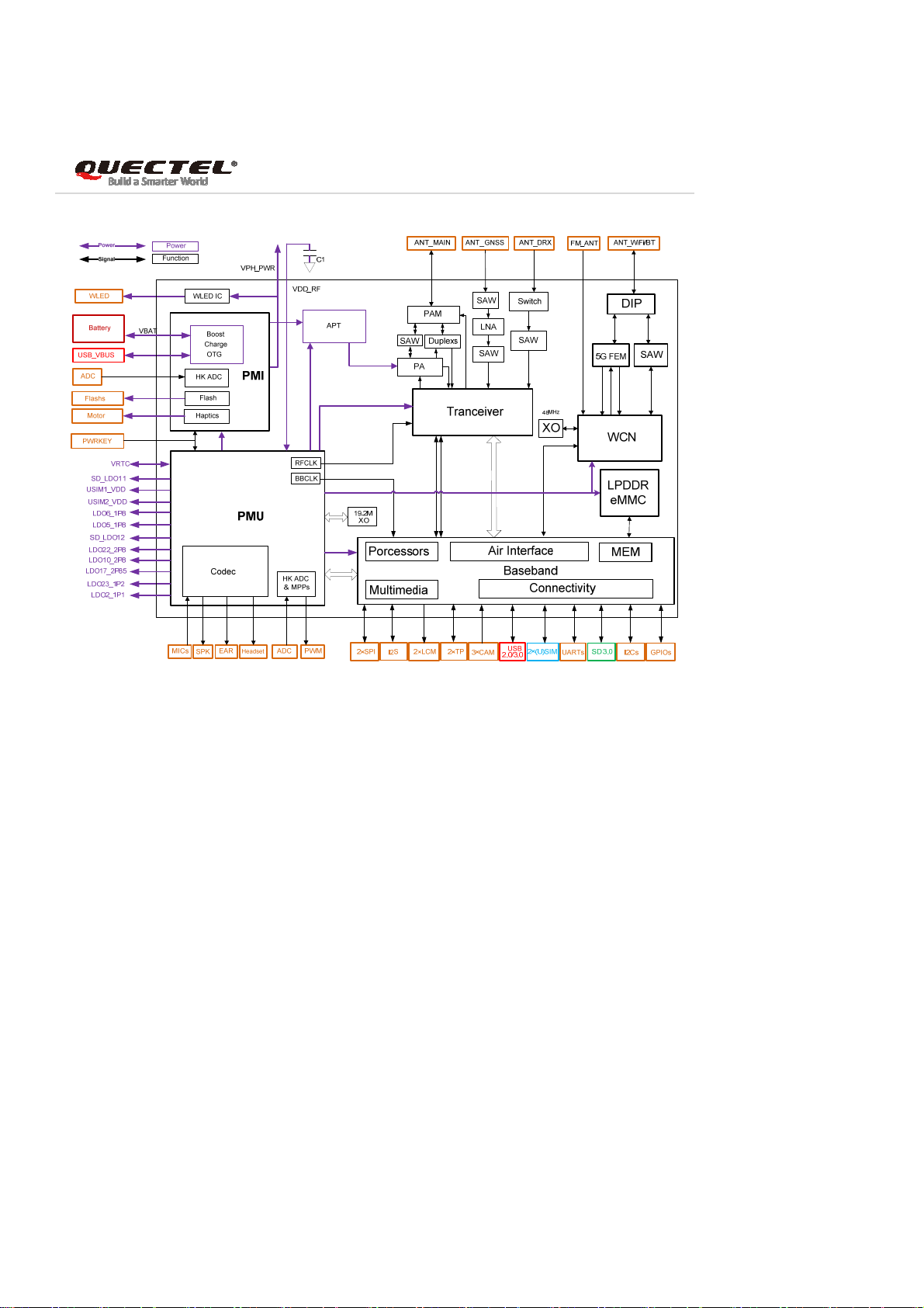
2.3. Functional Diagram
The following figure shows a block diagram of SC600Y/SC600T and illustrates the major functional parts.
Power management
Radio frequency
Baseband
LPDDR3+eMMC flash
Peripheral interfaces
-- USB interface
-- UART interfaces
-- (U)SIM interfaces
-- SD card interface
-- GPIO interfaces
-- I2C interfaces
-- I2S interface
-- SPI interfaces
-- ADC interfaces
-- Vibrator Drive interface
-- LCM (MIPI) interfaces
-- TP (touch panel) interfaces
-- Camera (MIPI) interfaces
-- Flashlight interfaces
-- Sensor interfaces
-- Audio interfaces
-- Emergency Download interface
SC600Y&SC600T_Hardware_Design 17 / 134
Page 19
SC600Y&SC600T Hardware Design
Smart Module Series
Figure 1: Functional Diagram
2.4. Evaluation Board
In order to help customers develop applications with SC600Y/SC600T conveniently, Quectel supplies the
evaluation board, USB to RS232 converter cable, USB Type-C data cable, power adapter, earphone,
antenna and other peripherals to control or test the module. For more details, please refer to document
[1].
SC600Y&SC600T_Hardware_Design 18 / 134
Page 20

SC600Y&SC600T Hardware Design
Smart Module Series
3 Application Interfaces
3.1. General Description
SC600Y/SC600T is equipped with 323 pins that can be embedded into cellular application platform. The
following chapters provide the detailed description of pins/interfaces listed below.
Power supply
VRTC interface
Charging interface
USB interface
UART interfaces
(U)SIM interfaces
SD card interface
GPIO interfaces
I2C interfaces
I2S interface
SPI interfaces
ADC interfaces
Vibrator drive interface
LCM interfaces
TP (touch panel) interfaces
Camera interfaces
Flashlight interfaces
Sensor interfaces
Audio interfaces
Emergency download interface
SC600Y&SC600T_Hardware_Design 19 / 134
Page 21
SC600Y&SC600T Hardware Design
Smart Module Series
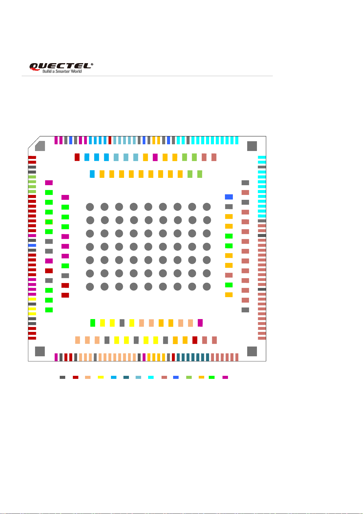
3.2. Pin Assignment
The following figure shows the pin assignment of SC600Y/SC600T module.
133
144
151
152
150
320
1
2
3
4
5
6
153
7
8
154
9
10
11
12
13
14
15
16
17
18
19
20
21
22
23
2
4
25
26
27
28
29
30
31
32
33
34
35
36
37
38
211
155
212
156
213
157
214
158
215
159
216
160
217
161
218
162
219
163
220
164
221
165
166
146
148
147
149
2
1
0
1
6
7
142
143
145
2
0
9
1
6
8
2
2
0
0
7
8
2
2
5
5
6
5
264
257
258
265
266
259
267
260
268
261
269
262
263
270
2
2
2
2
2
3
1
6
9
138
141
140
139
2
0
6
2
2
5
5
3
4
271
272
273
274
275
276
277
2
2
2
2
5
4
1
1
7
7
0
1
134
132
135
137
136
2
2
0
0
5
4
2
5
2
278
279
280
281
282
283
284
2
2
6
1
1
7
7
2
3
131
2
2
0
0
2
3
2
2
5
5
1
0
285
286
287
288
289
290
291
2
2
2
2
7
8
1
1
7
7
5
4
127
126
128
129
130
2
2
0
0
0
1
2
2
4
9
2
2
9
2
4
4
7
8
299
292
300
293
301
294
295
302
303
296
304
297
305
298
2
2
3
3
1
0
1
1
7
7
6
7
122
125
123
124
1
9
9
2
4
6
306
307
308
309
310
311
312
2
3
2
1
7
8
120
121
1
1
9
9
7
8
2
4
5
313
314
315
316
317
318
319
2
3
3
1
1
8
7
0
9
116
117
118
119
1
9
6
1
8
1
115
323
114
113
112
111
110
109
195
108
107
194
244
243
242
241
240
239
238
237
236
235
234
106
105
193
104
103
192
102
101
191
100
99
190
98
97
189
96
95
188
94
93
187
92
91
186
90
89
185
88
87
184
86
85
183
84
83
182
82
81
80
79
78
77
321
39
42
40
41
GND POWER AUDIO USB
46
49
50
47
48
45
44
43
51
(U)SIM SD TP LCM
555657585960616263
52
53
54
CAMERA ANT UART GPIO
64
656667
68
697071
RESERVED
72
737475
OTHERS
322
76
Figure 2: Pin Assignment (Top View)
SC600Y&SC600T_Hardware_Design 20 / 134
Page 22

SC600Y&SC600T Hardware Design
Smart Module Series
3.3. Pin Description
Table 6: I/O Parameters Definition
Type Description
AI Analog input
AO Analog output
DI Digital input
DO Digital output
IO Bidirectional
OD Open drain
PI Power input
PO Power output
The following tables show the SC600Y/SC600T’s pin definitions and electrical characteristics.
Table 7: Pin Description
Power Supply
Pin Name Pin No. I/O Description
VBAT
VDD_RF 1, 2
VPH_PWR 220, 221 PO
36, 37,
38
PI/
Power supply for the
PO
module
Connect to external
bypass capacitors to
eliminate voltage
fluctuation of RF part.
Power supply for
peripherals
DC
Characteristics
Vmax=4.4V
Vmin=3.55V
Vnorm=3.8V
Do not load externally.
Vmax=4.4V
Vmin=3.55V
Comment
It must be provided
with sufficient current
up to 3.0A.
It is suggested to use a
TVS to increase
voltage surge
withstand capability.
It can provide a
maximum continuous
SC600Y&SC600T_Hardware_Design 21 / 134
Page 23

SC600Y&SC600T Hardware Design
Smart Module Series
Vnorm=3.8V current of 1A
approximately.
The value of capacitors
placed on this pin
should not exceed
120uF.
VRTC 16
PI/PO Power supply for
internal RTC circuit
max=3.2V
V
O
=2.0V~3.25V
V
I
Power supply for
LDO5_1P8 9 PO
1.8V output power
supply
Vnorm=1.8V
max=20mA
I
O
external GPIO’s pull up
circuits and level shift
circuit.
Power supply for VDD
of sensors and TPs.
Add a 1.0uF~4.7uF
bypass capacitor if
used.
LDO10_2P8 11 PO
2.8V output power
supply
Vnorm=2.8V
max=150mA
I
O
If unused, keep this pin
open.
Power supply for I/O
VDD of cameras,
LCDs and sensors.
LDO6_1P8 10 PO
1.8V output power
supply
Vnorm=1.8V
max=300mA
I
O
Add a 1.0uF~2.2uF
bypass capacitor if
used.
If unused, keep this pin
open.
Power supply for
cameras and LCDs.
Add a 1.0uF~4.7uF
bypass capacitor if
used.
LDO17_2P85 12 PO
2.85V output power
supply
Vnorm=2.85V
max=300mA
I
O
If unused, keep this pin
open.
Power supply for
DVDD of front camera.
Add a 1.0uF~2.2uF
bypass capacitor if
used.
LDO23_1P2 15 PO
1.2V output power
supply
Vnorm=1.2V
max=600mA
I
O
If unused, keep this pin
open.
SC600Y&SC600T_Hardware_Design 22 / 134
Page 24

SC600Y&SC600T Hardware Design
Smart Module Series
Power supply for
DVDD of rear camera.
Add a 1.0uF~2.2uF
bypass capacitor if
used.
LDO2_1P1 13 PO
1.1V output power
supply
Vnorm=1.1V
max=1200mA
I
O
If unused, keep this pin
open.
Power supply for
AVDD of camera.
Add a 1.0uF~4.7uF
bypass capacitor if
used.
LDO22_2P8 14 PO
2.8V output power
supply
Vnorm=2.8V
max=150mA
I
O
If unused, keep this pin
open.
3, 4, 18,
20, 31,
34, 35,
40, 43,
47, 56,
62, 87,
98, 101,
112, 125,
GND
128, 130,
133, 135,
Ground
148, 150,
159, 163,
170, 173,
176, 182,
193, 195,
219, 225,
243,
257~323
Audio Interfaces
Pin Name Pin No. I/O Description
MIC_BIAS 167 AO
MIC1_P 44 AI
MIC1_N 45 AI
MIC_GND 168
Microphone bias
voltage
Microphone input for
channel 1 (+)
Microphone input for
channel 1 (-)
Microphone
reference ground
DC
Characteristics
=1.6V~2.85V
V
O
Comment
If unused, connect this
pin to the ground.
SC600Y&SC600T_Hardware_Design 23 / 134
Page 25

SC600Y&SC600T Hardware Design
Smart Module Series
MIC2_P 46 AI
MIC3_P 169 AI
Microphone input for
headset (+)
Microphone input for
channel 2 (+)
EAR_P 53 AO Earpiece output (+)
EAR_N 52 AO Earpiece output (-)
SPK_P 55 AO Speaker output (+)
SPK_N 54 AO Speaker output (-)
HPH_R 51 AO
HPH_REF 50 AI
HPH_L 49 AO
HS_DET 48 AI
LINE_OUT_P 227 AO
LINE_OUT_N 228 AO
Headphone right
channel output
Headphone
reference ground
Headphone left
channel output
Headset insertion
detection
Audio line differential
(+)
Audio line differential
(-)
It should be connected
to main
GND.
Pulled up internally.
USB Interface
Pin Name Pin No. I/O Description DC Characteristics Comment
Charging power input.
USB_VBUS 41, 42
Power supply output
PI/
for OTG device
PO
USB/charger insertion
Vmax=10V
Vmin=4.0V
Vnorm=5.0V
detection
AI/
USB_DM 33
USB_DP 32
USB 2.0 differential
AO
data bus (-)
AI/
USB 2.0 differential
AO
data bus (+)
USB_ID 30 AI USB ID detection
USB_SS_RX
_P
USB_SS_RX
_M
171 AI
172 AI
USB 3.0 differential
receive data (+)
USB 3.0 differential
receive data (-)
90Ω differential
impedance.
USB 2.0 standard
compliant.
High level by default.
90Ω differential
impedance.
USB 3.0 standard
compliant.
SC600Y&SC600T_Hardware_Design 24 / 134
Page 26

SC600Y&SC600T Hardware Design
Smart Module Series
USB_SS_TX
_P
USB_SS_TX
_M
174 AO
175 AO
USB 3.0 differential
transmit data (+)
USB 3.0 differential
transmit data (-)
USB Type-C control
USBC_CC2 223 AI
configuration channel
2
USB Type-C control
USBC_CC1 224 AI
configuration channel
1
USB_SS_SEL 226 DO
USB Type-C switch
control
If Micro USB is
intended to be used,
this pin should be
USB_OPT 217
Type-C/Micro USB
select control
connected to ground
via a 1KΩ resistor;
If Type-C is intended to
be used, this pin
should be left open.
(U)SIM Interfaces
Pin Name Pin No. I/O Description DC Characteristics Comment
Active low.
Require external
pull-up to 1.8V.
If unused, keep this
pin open.
Disabled by default
USIM1_DET 145 DI
(U)SIM1 card
hot-plug detection
max=0.63V
V
IL
min=1.17V
V
IH
and can be enabled
through software
configuration.
V
max=0.4V
OL
USIM1_RST 144 DO (U)SIM1 card reset
min=
V
OH
0.8 × USIM1_VDD
V
max=0.4V
OL
USIM1_CLK 143 DO (U)SIM1 card clock
min=
V
OH
0.8 × USIM1_VDD
max=
V
IL
0.2 × USIM1_VDD
USIM1_DATA 142 IO (U)SIM1 card data
V
min=
IH
0.7 × USIM1_VDD
max=0.4V
V
OL
SC600Y&SC600T_Hardware_Design 25 / 134
Page 27

SC600Y&SC600T Hardware Design
Smart Module Series
VOHmin=
0.8 × USIM1_VDD
1.8V (U)SIM:
Vmax=1.90V
USIM1_VDD 141 PO
(U)SIM1 card power
supply
Vmin=1.70V
2.95V (U)SIM:
Either 1.8V or 2.95V
(U)SIM card is
supported.
Vmax=3.04V
Vmin=2.7V
Active low.
Require external
pull-up to 1.8V.
If unused, keep this pin
open.
Disabled by default
USIM2_DET 256 DI
(U)SIM2 card
hot-plug detection
max=0.63V
V
IL
min=1.17V
V
IH
and can be enabled
through software
configuration.
V
max=0.4V
OL
USIM2_RST 207 DO (U)SIM2 card reset
min=
V
OH
0.8 × USIM2_VDD
V
max=0.4V
OL
USIM2_CLK 208 DO (U)SIM2 card clock
min=
V
OH
0.8 × USIM2_VDD
V
max=
IL
0.2 × USIM2_VDD
min=
V
IH
USIM2_DATA 209 IO (U)SIM2 card data
0.7 × USIM2_VDD
max=0.4V
V
OL
min=
V
OH
0.8 × USIM2_VDD
1.8V (U)SIM:
Vmax=1.90V
USIM2_VDD 210 PO
(U)SIM2 card power
supply
Vmin=1.70V
2.95V (U)SIM:
Either 1.8V or 2.95V
(U)SIM card is
supported.
Vmax=3.04V
Vmin=2.7V
UART Interfaces
Pin Name Pin No. I/O Description DC Characteristics Comment
UART2_TXD 5 DO
UART2 transmit data.
Used for debugging
max=0.45V
V
OL
min=1.35V
V
OH
1.8V power domain.
If unused, keep these
SC600Y&SC600T_Hardware_Design 26 / 134
Page 28

SC600Y&SC600T Hardware Design
Smart Module Series
by default pins open.
UART2 receive data.
UART2_RXD 6 DI
Used for debugging
by default
UART4_TXD 7 DO UART4 transmit data
UART4_RXD 8 DI UART4 receive data
UART5_RXD 198 DI UART5 receive data
UART5_TXD 199 DO UART5 transmit data
UART5_RTS 245 DO
UART5 request to
send
UART5_CTS 246 DI UART5 clear to send
max=0.63V
V
IL
min=1.17V
V
IH
max=0.45V
V
OL
min=1.35V
V
OH
max=0.63V
V
IL
min=1.17V
V
IH
max=0.63V
V
IL
min=1.17V
V
IH
max=0.45V
V
OL
min=1.35V
V
OH
max=0.45V
V
OL
min=1.35V
V
OH
max=0.63V
V
IL
min=1.17V
V
IH
SD Card Interface
Pin Name Pin No. I/O Description DC Characteristics Comment
1.8V SD card:
max=0.45V
V
OL
min=1.4V
V
OH
SD_CLK 70 DO SD card clock
2.95V SD card:
max=0.37V
V
OL
min=2.2V
V
OH
1.8V SD card:
V
max=0.58V
IL
min=1.27V
V
IH
max=0.45V
V
OL
min=1.4V
V
OH
SD_CMD 69 IO SD card command
2.95V SD card:
max=0.73V
V
IL
min=1.84V
V
IH
max=0.37V
V
OL
min=2.2V
V
OH
1.8V SD card:
SD_DATA0 68 IO SD card data
VILmax=0.58V
min=1.27V
V
IH
SC600Y&SC600T_Hardware_Design 27 / 134
Page 29

SC600Y&SC600T Hardware Design
Smart Module Series
V
max=0.45V
OL
min=1.4V
V
SD_DATA1 67 IO
OH
2.95V SD card:
max=0.73V
V
SD_DATA2 66 IO
SD_DATA3 65 IO
IL
min=1.84V
V
IH
max=0.37V
V
OL
min=2.2V
V
OH
SD_DET 64 DI
SD_LDO11 63 PO
SD card insertion
detection
Power supply for SD
card
SD_LDO12 179 PO 1.8V/2.95V output
max=0.63V
V
IL
min=1.17V
V
IH
Vnorm=2.95V
max=800mA
I
O
Vnorm=1.8V/2.95V
max=50mA
I
O
Active low.
Power supply for SD
card’s pull-up circuit.
TP (Touch Panel) Interfaces
Pin Name Pin No. I/O Description DC Characteristics Comment
TP0_RST 138 DO TP0 reset
TP0_INT 139 DI TP0 interrupt
max=0.45V
V
OL
min=1.35V
V
OH
max=0.63V
V
IL
min=1.17V
V
IH
1.8V power domain.
Active low.
1.8V power domain.
TP0_I2C_SCL 140 OD TP0 I2C clock 1.8V power domain.
TP0_I2C_SDA 206 OD TP0 I2C data 1.8V power domain.
TP1_RST 136 DO TP1 reset
TP1_INT 137 DI TP1 interrupt
max=0.45V
V
OL
min=1.35V
V
OH
max=0.63V
V
IL
min=1.17V
V
IH
1.8V power domain.
Active low.
1.8V power domain.
TP1_I2C_SDA 204 OD TP1 I2C data 1.8V power domain.
TP1_I2C_SCL 205 OD TP1 I2C clock 1.8V power domain.
LCM Interfaces
Pin Name Pin No. I/O Description DC Characteristics Comment
SC600Y&SC600T_Hardware_Design 28 / 134
Page 30

SC600Y&SC600T Hardware Design
Smart Module Series
LCD_BL_A 21 PO
LCD_BL_K1 22 AI
LCD_BL_K2 23 AI
LCD_BL_K3 24 AI
LCD_BL_K4 25 AI
PMU_MPP4 152 DO PWM output
LCD0_RST 127 DO LCD0 reset
LCD0_TE 126 DI LCD0 tearing effect
LCD1_RST 113 DO LCD1 reset
LCD1_TE 114 DI LCD1 tearing effect
DSI0_CLK_N 116 AO
DSI0_CLK_P 115 AO
DSI0_LN0_N 118 AO
DSI0_LN0_P 117 AO
DSI0_LN1_N 120 AO
DSI0_LN1_P 119 AO
DSI0_LN2_N 122 AO
DSI0_LN2_P 121 AO
DSI0_LN3_N 124 AO
Current output for
LCD backlight
Current sink for LCD
backlight
Current sink for LCD
backlight
Current sink for LCD
backlight
Current sink for LCD
backlight
LCD0 MIPI clock
signal (-)
LCD0 MIPI clock signal
(+)
LCD0 MIPI lane 0 data
signal (-)
LCD0 MIPI lane 0 data
signal (+)
LCD0 MIPI lane 1 data
signal (-)
LCD0 MIPI lane 1 data
signal (+)
LCD0 MIPI lane 2 data
signal (-)
LCD0 MIPI lane 2 data
signal (+)
LCD0 MIPI lane 3 data
signal (-)
V
OL
V
OH
V
OL
V
OH
V
IL
V
IH
V
OL
V
OH
V
IL
V
IH
max=0.45V
min=1.35V
max=0.45V
min=1.35V
max=0.63V
min=1.17V
max=0.45V
min=1.35V
max=0.63V
min=1.17V
1.8V power domain.
Active low.
1.8V power domain.
1.8V power domain.
Active low.
1.8V power domain.
SC600Y&SC600T_Hardware_Design 29 / 134
Page 31

SC600Y&SC600T Hardware Design
Smart Module Series
DSI0_LN3_P 123 AO
DSI1_CLK_N 103 AO
DSI1_CLK_P 102 AO
DSI1_LN0_N 105 AO
DSI1_LN0_P 104 AO
DSI1_LN1_N 107 AO
DSI1_LN1_P 106 AO
DSI1_LN2_N 109 AO
DSI1_LN2_P 108 AO
DSI1_LN3_N 111 AO
DSI1_LN3_P 110 AO
LCD0 MIPI lane 3 data
signal (+)
LCD1 MIPI clock signal
(-)
LCD1 MIPI clock signal
(+)
LCD1 MIPI lane 0 data
signal (-)
LCD1 MIPI lane 0 data
signal (+)
LCD1 MIPI lane 1 data
signal (-)
LCD1 MIPI lane 1 data
signal (+)
LCD1 MIPI lane 2 data
signal (-)
LCD1 MIPI lane 2 data
signal (+)
LCD1 MIPI lane 3 data
signal (-)
LCD1 MIPI lane 3 data
signal (+)
Camera Interfaces
Pin Name Pin No. I/O Description
CSI0_CLK_N 89 AO
CSI0_CLK_P 88 AO
CSI0_LN0_N 91 AI
CSI0_LN0_P 90 AI
CSI0_LN1_N 93 AI
CSI0_LN1_P 92 AI
CSI0_LN2_N 95 AI
CSI0_LN2_P 94 AI
MIPI clock signal of
rear camera (-)
MIPI clock signal of
rear camera (+)
MIPI lane 0 data signal
of rear camera (-)
MIPI lane 0 data signal
of rear camera (+)
MIPI lane 1 data signal
of rear camera (-)
MIPI lane 1 data signal
of rear camera (+)
MIPI lane 2 data signal
of rear camera (-)
MIPI lane 2 data signal
of rear camera (+)
DC
Characteristics
Comment
SC600Y&SC600T_Hardware_Design 30 / 134
Page 32

SC600Y&SC600T Hardware Design
Smart Module Series
CSI0_LN3_N 97 AI
CSI0_LN3_P 96 AI
CSI1_CLK_N 184 AO
CSI1_CLK_P 183 AO
CSI1_LN0_N 186 AI
CSI1_LN0_P 185 AI
CSI1_LN1_N 188 AI
CSI1_LN1_P 187 AI
CSI1_LN2_N 190 AI
CSI1_LN2_P 189 AI
CSI1_LN3_N 192 AI
CSI1_LN3_P 191 AI
CSI2_CLK_N 78 AO
CSI2_CLK_P 77 AO
CSI2_LN0_N 80 AI
CSI2_LN0_P 79 AI
CSI2_LN1_N 82 AI
CSI2_LN1_P 81 AI
CSI2_LN2_N 84 AI
MIPI lane 3 data signal
of rear camera (-)
MIPI lane 3 data signal
of rear camera (+)
MIPI clock signal of
depth camera (-)
MIPI clock signal of
depth camera (+)
MIPI lane 0 data signal
of depth camera (-)
MIPI lane 0 data signal
of depth camera (+)
MIPI lane 1 data signal
of depth camera (-)
MIPI lane 1 data signal
of depth camera (+)
MIPI lane 2 data signal
of depth camera (-)
MIPI lane 2 data signal
of depth camera (+)
MIPI lane 3 data signal
of depth camera (-)
MIPI lane 3 data signal
of depth camera (+)
MIPI clock signal of
front camera (-)
MIPI clock signal of
front camera (+)
MIPI lane 0 data signal
of front camera (-)
MIPI lane 0 data signal
of front camera (+)
MIPI lane 1 data signal
of front camera (-)
MIPI lane 1 data signal
of front camera (+)
MIPI lane 2 data signal
of front camera (-)
Can be multiplexed
into differential data of
the fourth camera (-).
Can be multiplexed
into differential data of
the fourth camera (+).
Can be multiplexed
into differential clock of
the fourth camera (-).
Can be multiplexed
into differential clock of
the fourth camera (+).
SC600Y&SC600T_Hardware_Design 31 / 134
Page 33

SC600Y&SC600T Hardware Design
Smart Module Series
CSI2_LN2_P 83 AI
CSI2_LN3_N 86 AI
CSI2_LN3_P 85 AI
MCAM_MCLK 99 DO
SCAM_MCLK 100 DO
MIPI lane 2 data signal
of front camera (+)
MIPI lane 3 data signal
of front camera (-)
MIPI lane 3 data signal
of front camera (+)
Master clock of rear
camera
Master clock of front
camera
MCAM_RST 74 DO Reset of rear camera
MCAM_PWDN 73 DO
Power down of rear
camera
SCAM_RST 72 DO Reset of front camera
SCAM_PWDN 71 DO
Power down of front
camera
max=0.45V
V
OL
min=1.35V
V
OH
max=0.45V
V
OL
min=1.35V
V
OH
max=0.45V
V
OL
min=1.35V
V
OH
max=0.45V
V
OL
min=1.35V
V
OH
max=0.45V
V
OL
min=1.35V
V
OH
max=0.45V
V
OL
min=1.35V
V
OH
1.8V power domain.
1.8V power domain.
1.8V power domain.
1.8V power domain.
1.8V power domain.
1.8V power domain.
CAM_I2C_SCL 75 OD I2C clock for camera 1.8V power domain.
CAM_I2C_SDA 76 OD I2C data for camera 1.8V power domain.
DCAM_MCLK 194 DO
CAM4_MCLK 236 DO
Master clock of depth
camera
Master clock of fourth
camera
DCAM_RST 180 DO Reset of depth camera
DCAM_PWDN 181 DO
DCAM_I2C_
SDA
DCAM_I2C_
SCL
197 OD
196 OD
Power down of depth
camera
I2C data for depth
camera
I2C clock for depth
camera
max=0.45V
V
OL
min=1.35V
V
OH
max=0.45V
V
OL
min=1.35V
V
OH
max=0.45V
V
OL
min=1.35V
V
OH
max=0.45V
V
OL
min=1.35V
V
OH
1.8V power domain.
1.8V power domain.
1.8V power domain.
1.8V power domain.
1.8V power domain.
1.8V power domain.
Keypad Interfaces
Pin Name Pin No. I/O Description
DC
Characteristics
Comment
SC600Y&SC600T_Hardware_Design 32 / 134
Page 34

SC600Y&SC600T Hardware Design
Smart Module Series
PWRKEY 39 DI Turn on/off the module
VOL_UP 146 DI Volume up
VOL_
DOWN
147 DI Volume down
SENSOR_I2C Interface
Pin Name Pin No. I/O Description
SENSOR_I2C_
SCL
SENSOR_I2C_
SDA
131 OD
132 OD
I2C clock for external
sensors
I2C data for external
sensors
ADC Interfaces
Pin Name Pin No. I/O Description
PMI_ADC 153 AI
General purpose ADC
interface
max=0.63V
V
IL
min=1.17V
V
IH
max=0.63V
V
IL
min=1.17V
V
IH
max=0.63V
V
IL
min=1.17V
V
IH
DC
Characteristics
Pull-up to 1.8V
internally.
Active low.
If unused, keep this pin
open.
If unused, keep this pin
open.
Comment
1.8V power domain.
1.8V power domain.
DC
Characteristics
Comment
Maximum input
voltage: 1.5V.
PMU_MPP2 151 AI
General purpose ADC
interface
Maximum input
voltage: 1.7V.
Charging Interface
Pin Name Pin No. I/O Description
DC
Characteristics
Comment
Differential input of
BAT_PLUS 27 AI
battery voltage
Must be connected.
detection (+)
Differential input of
BAT_MINUS 28 AI
battery voltage
Must be connected.
detection (-)
Antenna Interfaces
Pin Name Pin No. I/O Description
ANT_MAIN 19
ANT_DRX 149 AI
AI/
Main antenna interface
AO
Diversity antenna
interface
DC
Characteristics
Comment
50Ω impedance.
SC600Y&SC600T_Hardware_Design 33 / 134
Page 35

SC600Y&SC600T Hardware Design
Smart Module Series
ANT_GNSS 134 AI
ANT_WIFI/BT 129
GNSS antenna
interface
AI/
Wi-Fi/BT antenna
AO
interface
ANT_FM 244 AI FM antenna interface
GPIO Interfaces
Pin Name Pin No. I/O Description
GPIO_0 248 IO
GPIO_1 247 IO
GPIO_2 201 IO
GPIO_3 200 IO
GPIO_33 238 IO
GPIO_36 237 IO
GPIO_42 252 IO
GPIO_43 253 IO
GPIO_44 254 IO
GPIO_45 255 IO
GPIO_66 234 IO
GPIO_89 232 IO
GPIO_90 231 IO
GPIO_96 230 IO
GPIO_97 229 IO
GPIO_98 177 IO
General-purpose
input/output
General-purpose
input/output
General-purpose
input/output
General-purpose
input/output
General-purpose
input/output
General-purpose
input/output
General-purpose
input/output
General-purpose
input/output
General-purpose
input/output
General-purpose
input/output
General-purpose
input/output
General-purpose
input/output
General-purpose
input/output
General-purpose
input/output
General-purpose
input/output
General-purpose
input/output
DC
Characteristics
max=0.63V
V
IL
min=1.17V
V
IH
max=0.45V
V
OL
min=1.4V
V
OH
Comment
SC600Y&SC600T_Hardware_Design 34 / 134
Page 36

SC600Y&SC600T Hardware Design
Smart Module Series
GPIO_99 178 IO
General-purpose
input/output
SPI Interfaces
Pin Name Pin No. I/O Description
DC
Characteristics
SPI_CS 58 DO SPI chip select
SPI_CLK 59 DO SPI clock
SPI_MOSI 60 DO SPI master-out slave-in
SPI_MISO 61 DI SPI master-in salve-out
FP_SPI_CS 203 DO SPI chip select
FP_SPI_CLK 250 DO SPI clock
FP_SPI_MOSI 249 DO SPI master-out slave-in
FP_SPI_MISO 251 DI SPI master-in salve-out
Comment
Can be multiplexed
into UART6_CTS.
Can be multiplexed
into UART6_RTS.
Can be multiplexed
into UART6_TXD.
Can be multiplexed
into UART6_RXD.
Can be multiplexed
into I2S_WS.
Can be multiplexed
into I2S_SCK.
Can be multiplexed
into I2S_D0.
Can be multiplexed
into I2S_D1.
Vibrator Drive Interface
Pin Name Pin No. I/O Description
VIB_GND 160
Vibrator ground
(-)
DC
Characteristics
Comment
Connected to the
negative terminal of
vibrator.
Connected to the
VIB_DRV 161 PO Vibrator drive (+)
positive terminal of
vibrator.
Flashlight Interfaces
Pin Name Pin No. I/O Description
FLASH_LED1 26 AO
FLASH_LED2 162 AO
Flash/torch current
driver output
Flash/torch current
driver output
DC
Characteristics
Comment
Support flash and torch
modes.
Emergency Download Interface
Pin Name Pin No. I/O Description
DC
Characteristics
Comment
SC600Y&SC600T_Hardware_Design 35 / 134
Page 37

SC600Y&SC600T Hardware Design
Smart Module Series
Pulled up to
LDO5_1P8 during
power-up will force the
module to enter
emergency download
USB_BOOT 57 DI
Force the module enter
emergency download
mode
mode.
Other Interfaces
Pin Name Pin No. I/O Description
BAT_ID 17 AI Battery type detection
DC
Characteristics
Comment
If unused, keep this pin
open.
Internally pulled up.
BAT_THERM 29 AI
Battery temperature
measurement
Externally connected
to GND via a 47K NTC
resistor.
For test purpose only.
GNSS_LNA_EN 202 DO LNA enable control
If unused, keep this pin
open.
GRFC_5 242 IO Generic RF control 1
GRFC_7 241 IO Generic RF control 2
S1A 215
S1A and S1B are
Only used for RF tuner
control.
connected in the
S1B 216
S2A 211
module
S2A and S2B are
connected in the
S2B 233
module
Reserved Interface
Pin Name Pin No. I/O Description
DC
Characteristics
Comment
154, 155,
156, 157,
158, 164,
RESERVED
165, 166,
212, 213,
Reserved Keep these pins open.
214, 218,
222, 235,
239, 240,
SC600Y&SC600T_Hardware_Design 36 / 134
Page 38

SC600Y&SC600T Hardware Design
Smart Module Series
3.4. Power Supply
3.4.1. Power Supply Pins
SC600Y/SC600T provides 3 VBAT pins and 2 VPH_PWR pins. VBAT pins are dedicated for connection
with an external power supply. VPH_PWR pins can supply power for peripherals, and it can provide a
maximum continuous current of 1A approximately. The value of capacitors placed on this pin should not
exceed 120uF.
3.4.2. Decrease Voltage Drop
The power supply range of the module is from 3.55V to 4.4V, and the recommended value is 3.8V. The
power supply performance, such as load capacity, voltage ripple, etc. directly influences the module’s
performance and stability. Under ultimate conditions, the module may have a transient peak current up to
3A. If the power supply capability is not sufficient, there will be voltage drops, and if the voltage drops
below 3.1V, the module will be powered off automatically. Therefore, please make sure the input voltage
will never drop below 3.1V.
Figure 3: Voltage Drop Sample
To decrease voltage drop, a bypass capacitor of about 100µF with low ESR (ESR=0.7Ω) should be used
in VBAT pins, and a multi-layer ceramic chip capacitor (MLCC) array should also be reserved due to its
ultra-low ESR. It is recommended to use three ceramic capacitors (100nF, 33pF, 10pF) for composing the
MLCC array, and place these capacitors close to VBAT/VDD_RF/VPH_PWR pins. The width of VBAT
trace should be no less than 3mm. In principle, the longer the VBAT trace is, the wider it will be.
SC600Y&SC600T_Hardware_Design 37 / 134
Page 39

SC600Y&SC600T Hardware Design
Smart Module Series
In addition, in order to get a stable power source, it is suggested to use a 0.5W TVS and place it as close
to the VBAT pins as possible to increase voltage surge withstand capability. The following figure shows
the structure of the power supply.
Figure 4: Star Structure of Power Supply
3.4.3. Reference Design for Power Supply
The power design for the module is very important, as the performance of module largely depends on the
power source. The power supply of SC600Y/SC600T should be able to provide sufficient current up to 3A
at least. By default, it is recommended to use a battery to supply power for SC600Y/SC600T. But if
battery is not intended to be used, it is recommended to use a regulator for SC600Y/SC600T. If the
voltage difference between the input and output is not too high, it is suggested to use an LDO to supply
power for the module. If there is a big voltage difference between the input source and the desired output
(VBAT), a buck converter is preferred to be used as the power supply.
The following figure shows a reference design for +5V input power source which adopts an LDO
(MIC29502WU) from MICROCHIP. The typical output voltage is 3.8V and the maximum rated current is
5.0A.
Figure 5: Reference Circuit of Power Supply
SC600Y&SC600T_Hardware_Design 38 / 134
Page 40

SC600Y&SC600T Hardware Design
NOTES
1. It is recommended to switch off the power supply for module in abnormal state, and then switch on
the power to restart the module.
2. The module supports battery charging function by default. If the above power supply design is
adopted, please make sure the charging function is disabled by software, or connect VBAT to
Schottky diode in series to avoid the reverse current to the power supply chip.
3. When the battery power is reduced to 0%, the system will trigger automatic shutdown, so the design
of power supply should be consistent with the configuration of fuel gauge driver.
Smart Module Series
3.5. T u rn on and off Timing
3.5.1. Turn on Module Using the PWRKEY
The module can be turned on by driving PWRKEY pin to a low level for at least 1.6s. PWRKEY pin is
pulled to 1.8V internally. It is recommended to use an open drain/collector driver to control the PWRKEY.
A simple reference circuit is illustrated in the following figure.
Figure 6: Turn on the Module Using Driving Circuit
SC600Y&SC600T_Hardware_Design 39 / 134
Page 41

SC600Y&SC600T Hardware Design
Smart Module Series
Another way to control the PWRKEY is using a button directly. A TVS component is indispensable to be
placed nearby the button for ESD protection. A reference circuit is shown in the following figure.
Figure 7: Turn on the Module Using Keystroke
The timing of turning on is illustrated in the following figure.
VBAT(Typ.:3.8V)
PWRKEY
LDO5_1P8
LDO6_1P8
LDO10_2P8
LDO17_2P85
Others
Note2
>1.6s
61. 2ms
Softwar e
controlled
Softwar e
controlled
38s
Figure 8: Timing o f Turning on Module
Active
SC600Y&SC600T_Hardware_Design 40 / 134
Page 42

SC600Y&SC600T Hardware Design
NOTES
1. The turn-on timing might be different from the above figure when the module powers on for the first
time.
2. Make sure that VBAT is stable before pulling down PWRKEY pin. The recommended time between
them is no less than 30ms. PWRKEY cannot be pulled down all the time.
Smart Module Series
3.5.2. Turn off Module
Pull down PWRKEY for at least 1s, and then choose to turn off the module when a prompt window comes
up.
Another way to turn off the module is to drive PWRKEY to a low level for at least 8s. The module will
execute forced shutdown.
The forced power-down timing is illustrated in the following figure.
Figure 9: Timing of Turning off Module
SC600Y&SC600T_Hardware_Design 41 / 134
Page 43

SC600Y&SC600T Hardware Design
Smart Module Series
3.6. VRTC Interface
The RTC (Real Time Clock) can be powered by an external power source through VRTC when the
module is powered down and there is no power supply for the VBAT. The external power source can be
rechargeable battery (such as coil cells) according to application demands. The following reference circuit
design when an external battery is utilized for powering RTC.
Figure 10: RTC Powered by Coin Cell
If RTC is ineffective, it can be synchronized through network after the module is powered on.
2.0V~3.25V input voltage range and 3.0V typical value for VRTC, when VBAT is disconnected.
When powered by VBAT, the RTC error is 50ppm. When powered by VRTC, the RTC error is about
200ppm.
If the rechargeable battery is used, the ESR of battery should be less than 2KΩ, and it is
recommended to use the MS621FE FL11E of SEIKO.
SC600Y&SC600T_Hardware_Design 42 / 134
Page 44

SC600Y&SC600T Hardware Design
Smart Module Series
3.7. Power Output
SC600Y/SC600T supports output of regulated voltages for peripheral circuits. During application, it is
recommended to use parallel capacitors (33pF and 10pF) in the circuit to suppress high frequency noise.
Table 8: Power Description
Pin Name Default Voltage (V) Drive Current (mA) Idle
LDO5_1P8 1.8 20 Keep
LDO6_1P8 1.8 300 /
LDO10_2P8 2.8 150 /
LDO17_2P85 2.85 300 /
LDO2_1P1 1.1 1200 /
LDO22_2P8 2.8 150 /
LDO23_1P2 1.2 600 /
SD_LDO12 1.8/2.95 50 /
SD_LDO11 2.95 800 /
USIM1_VDD 1.8/2.95 50 /
USIM2_VDD 1.8/2.95 50 /
VPH_PWR Equal to VBAT voltage 1000 Keep
SC600Y&SC600T_Hardware_Design 43 / 134
Page 45

SC600Y&SC600T Hardware Design
Smart Module Series
3.8. Battery Charge and Management
SC600Y/SC600T supports a fully programmable switch-mode Li-ion battery charge function. It can
charge single-cell Li-ion and Li-polymer batteries. The battery charger of SC600Y/SC600T supports
trickle charging, pre-charge, constant current charging and constant voltage charging modes, which
optimize the charging procedure for Li-ion and Li-polymer batteries.
Trickle charging: When the battery voltage is below 2.1V, a 75mA trickle charging current is applied
to the battery.
Pre-charge: When the battery voltage is charged up and exceeds 2.1V (the maximum pre-charge
voltage is 2.3V~3.0V programmable, 3.0V by default), the system will enter into pre-charge mode.
The charging current is 250mA (100mA~450mA programmable, 250mA by default).
Constant current mode (CC mode): When the battery voltage is increased to between the
maximum pre-charge voltage and 4.35V (3.6V~4.35V programmable, 4.35V by default), the system
will switch to CC mode. The charging current is programmable from 300mA~3000mA. The default
charging current is 500mA for USB charging and 2A for adapter.
Constant voltage mode (CV mode): When the battery voltage reaches the final value 4.35V, the
system will switch to CV mode and the charging current will decrease gradually. When the charging
current reduces to about 100mA, the charging is completed.
Table 9: Pin Definition of Charging Interface
Pin Name Pin No. I/O Description Comment
Charging power input
USB_VBUS 41, 42 PI/PO
VBAT
BAT_ID 17 AI Battery type detection
BAT_PLUS 27 AI
BAT_MINUS 28 AI
BAT_THERM 29 AI Battery temperature measurement
36, 37,
38
PI/PO Power supply for the module
Power supply output for OTG device
USB/charger insertion detection
Differential input of battery voltage
detection (+)
Differential input of battery voltage
detection (-)
Vmax=10V
Vmin=4.0V
Vnorm=5.0V
Vmax=4.4V
Vmin=3.55V
Vnorm=3.8V
If unused, keep this
pin open.
Must be connected.
Must be connected.
Internally pulled up.
Externally connected
to GND via a 47KΩ
NTC resistor.
SC600Y&SC600T_Hardware_Design 44 / 134
Page 46

SC600Y&SC600T Hardware Design
Smart Module Series
SC600Y/SC600T supports battery temperature detection in the condition that the battery integrates a
thermistor (47KΩ 1% NTC thermistor with B-constant of 4050KΩ by default; SDNT1608X473F4050FTF of
SUNLORD is recommended) and the thermistor is connected to BAT_THERM pin. If BAT_THERM pin is
not connected, there will be malfunctions such as boot error, battery charging failure, battery level display
error, etc.
A reference design for battery charging circuit is shown below.
Figure 11: Reference Design for Battery Charging Circuit
SC600Y/SC600T offers a fuel gauge algorithm which is able to accurately estimate the battery’s state by
current and voltage monitor techniques. Using precise measurements of battery voltage, current, and
temperature, the fuel gauge provides a dependable state of charge estimate throughout the entire life of
the battery and across a broad range of operating conditions. It effectively protects the battery from
over-discharging, and also allows users to estimate the battery life based on the battery level so as to
timely save important data before completely power-down.
Mobile devices such as mobile phone and handheld POS systems are powered by batteries. When
different batteries are utilized, the charging and discharging curve has to be modified correspondingly so
as to achieve the best effect.
If thermistor is not available in the battery, or adapter is utilized for powering the module, then there is only
a need for VBAT and GND connection. In this case, the system may be unable to detect the battery,
which will cause power-on failure. In order to avoid this, BAT_THERM should be connected to GND with a
47KΩ resistor. BAT_PLUS and BAT_MINUS must be connected, otherwise there may be abnormalities in
use of the module. Among them, BAT_PLUS and BAT_MINUS are used for battery level detection, and
they should be routed as differential pair to ensure accuracy.
SC600Y&SC600T_Hardware_Design 45 / 134
Page 47

SC600Y&SC600T Hardware Design
Smart Module Series
3.9. USB Interface
SC600Y/SC600T provides one USB 3.0/2.0 compliant integrated Universal Serial Bus (USB) interface,
which supports super speed (5Gbps) on USB 3.0, high speed (480Mbps) on USB 2.0, full speed (12Mbps)
modes as well as USB OTG function. This USB interface is used for AT command communication, data
transmission, software debugging and firmware upgrade.
The following table shows the pin definition of USB interface.
Table 10: Pin Definition of USB Interface
Pin Name Pin No. I/O Description Comment
Charging power input
USB_VBUS 41, 42 PI/PO
USB_DM 33 AI/AO USB 2.0 USB differential data (-)
USB_DP 32 AI/AO USB 2.0 USB differential data (+)
USB_ID 30 AI USB ID detection High level by default.
USB_SS_RX_P 171 AI USB 3.0 differential receive data (+)
USB_SS_RX_M 172 AI USB 3.0 differential receive data (-)
USB_SS_TX_P 174 AO USB 3.0 differential transmit data (+)
USB_SS_TX_M 175 AO USB 3.0 differential transmit data (-)
USBC_CC2 223 AI
USBC_CC1 224 AI
USB_SS_SEL 226 DO USB Type-C switch control
USB_OPT 217 Type-C/ Micro USB select control
Power supply output for OTG device
USB/charger insertion detection
USB Type-C control configuration
channel 2
USB Type-C control configuration
channel 1
Vmax=10V
Vmin=4.0V
Vnorm=5.0V
90Ω differential
impedance.
90Ω differential
impedance.
If Micro USB is
intended to be used,
this pin should be
connected to ground
via a 1KΩ resistor;
If Type-C is intended
to be used, this pin
should be left open.
SC600Y&SC600T_Hardware_Design 46 / 134
Page 48

SC600Y&SC600T Hardware Design
Smart Module Series
USB_VBUS can be powered by a USB power or an adapter. It is used for USB connection detection and
power supply input for battery charging. Its input voltage ranges from 4.0V to 10.0V, and the typical value
is 5.0V. SC600Y/SC600T supports charging management for a single cell Li-ion battery, but varied
charging parameters should be set for batteries with varied models or capacities. The maximum charging
current is up to 3.0A.
SC600Y/SC600T supports USB On-The-Go (OTG) function. USB_ID pin is used to detect whether the
OTG device is attached. If USB_ID is kept open (high level by default), the module will be in USB device
mode; if USB_ID is connected to ground, the module will be in host mode and the USB_VBUS is used to
supply power for peripherals with maximum output of 5V/1A.
The use of Type-C and Micro USB is up to the design of USB_OPT. If Micro USB is intended to be used,
USB_OPT should be connected to ground via a 1KΩ resistor, and if Type-C is intended to be used,
USB_OPT should be left open.
The following is a reference design for Micro USB interface:
Figure 12: Micro USB Interface Reference Design
SC600Y&SC600T_Hardware_Design 47 / 134
Page 49

SC600Y&SC600T Hardware Design
Smart Module Series
The following is a reference design for USB Type-C interface:
Module
USB_VBU S
USB_SS_TX_P
USB_SS_TX_M
USB_SS_RX_P
USB_SS_RX_M
USB_SS_SEL
USB_OPT
USB_DM
USB_DP
CC1
CC2
A0+
C2
C3
A0-
C4
A1+
C5
A0-
VDD_3V
R1
NM
C1
4.7uF
C14
100nF
SEL
VDD
PD
R2
C6
B0+
C7
B0-
C8
B1+
C9
B1-
C10
C0+
C11
C0-
C12
C1+
C13
C1-
USB Type- C
VUSB_ VBUS
D-
D+
CC
1
CC2
TX2+
TX2RX2+
RX2-
TX1+
TX1RX1+
RX1-
Switch
Figure 13: USB Type-C Interface Referen ce Design
In order to ensure USB performance, please follow the following principles while designing USB interface.
It is important to route the USB signal traces as differential pairs with total grounding. The impedance
of USB differential trace is 90Ω.
Pay attention to the influence of junction capacitance of ESD protection devices on USB data lines.
Typically, the capacitance value should be less than 2pF for USB 2.0 and less than 0.5pF for USB
3.0.
Do not route signal traces under crystals, oscillators, magnetic devices and RF signal traces. It is
important to route the USB differential traces in inner-layer with ground shielding on not only upper
and lower layers but also right and left sides.
Keep the ESD protection devices as close as possible to the USB connector.
Make sure the trace length difference between USB 2.0 DM/DP differential pair and that between
USB 3.0 RX/TX differential pairs both do not exceed 0.7mm.
Table 11: USB Trace Length Inside the Module
Pin No. Signal Length (mm) Length Difference (DP-DM)
33 USB_DM 39.52
-0.45
32 USB_DP 39.07
171 USB_SS_RX_P 28.55 0.32
SC600Y&SC600T_Hardware_Design 48 / 134
Page 50

SC600Y&SC600T Hardware Design
Smart Module Series
172 USB_SS_RX_M 28.23
174 USB_SS_TX_P 19.58
0.23
175 USB_SS_TX_M 19.35
3.10. UART Interfaces
The module provides the following four UART interfaces:
UART5: 4-wire UART interface, hardware flow control supported.
UART6: 4-wire UART interface, hardware flow control supported, multiplexed from SPI interface.
UART2: 2-wire UART interface, used for debugging.
UART4: 2-wire UART interface.
The following table shows the pin definition of UART interfaces.
Table 12: Pin Definition of UART Interfaces
Pin Name Pin No. I/O Description Comment
UART2_TXD 5 DO
UART2_RXD 6 DI
UART4_TXD 7 DO UART4 transmit data
UART4_RXD 8 DI UART4 receive data
UART5_RXD 198 DI UART5 receive data
UART5_TXD 199 DO UART5 transmit data
UART5_CTS 246 DI UART5 clear to send
UART5_RTS 245 DO UART5 request to send
SPI_MISO 61 DI UART6 receive data
SPI_MOSI 60 DO UART6 transmit data
UART2 transmit data.
Used for debugging by default
UART2 receive data.
Used for debugging by default
1.8V power domain.
If unused, keep these
pins open.
SPI interface pin by
default.
Can be multiplexed into
UART6_RXD.
SPI interface pin by
default.
SC600Y&SC600T_Hardware_Design 49 / 134
Page 51

SC600Y&SC600T Hardware Design
Smart Module Series
Can be multiplexed into
UART6_TXD.
SPI interface pin by
SPI_CS 58 DI UART6 clear to send
default.
Can be multiplexed into
UART6_CTS.
SPI interface pin by
SPI_CLK 59 DO UART6 request to send
default.
Can be multiplexed into
UART6_RTS.
UART5 is a 4-wire UART interface with 1.8V power domain. A level translator chip should be used if
customers’ application is equipped with a 3.3V UART interface. A level translator chip TXS0104EPWR
provided by Texas Instruments is recommended.
The following figure shows a reference design.
Figure 14: Reference Circuit with Level Translator Chip (for UART5)
SC600Y&SC600T_Hardware_Design 50 / 134
Page 52

SC600Y&SC600T Hardware Design
Smart Module Series
The following figure is an example of connection between SC600Y/SC600T and PC. A voltage level
translator and a RS-232 level translator chip are recommended to be added between the module and PC,
as shown below:
Figure 15: RS232 Level Match Circuit (for U ART5)
NOTE
UART2, UART4 and UART6 are similar to UART5. Please refer to UART5 reference circuit design for that
of the UART2, UART4 and UART6.
3.11. (U)SIM Interfaces
SC600Y/SC600T provides two (U)SIM interfaces which both meet ETSI and IMT-2000 requirements.
Dual SIM Dual Standby is supported by default. Both 1.8V and 2.95V (U)SIM cards are supported, and
the (U)SIM interfaces are powered by the dedicated low dropout regulators in SC600Y/SC600T module.
Table 13: Pin Definition of (U)SIM Interfaces
Pin Name Pin No. I/O Description Comment
Active Low.
Require external pull-up to 1.8V.
USIM1_DET 145 DI
(U)SIM1 card hot-plug
detection
If unused, keep this pin open.
Disabled by default, and can be
enabled through software
configuration.
SC600Y&SC600T_Hardware_Design 51 / 134
Page 53

SC600Y&SC600T Hardware Design
Smart Module Series
USIM1_RST 144 DO (U)SIM1 card reset
USIM1_CLK 143 DO (U)SIM1 card clock
USIM1_DATA 142 IO (U)SIM1 card data
USIM1_VDD 141 PO (U)SIM1 card power supply
Pull up to USIM1_VDD with a
10KΩ resistor.
Either 1.8V or 2.95V (U)SIM card
is supported.
Active low.
Require external pull-up to 1.8V.
USIM2_DET 256 DI
(U)SIM2 card hot-plug
detection
If unused, keep this pin open.
Disabled by default and can be
enabled through software
configuration.
USIM2_RST 207 DO (U)SIM2 card reset signal
USIM2_CLK 208 DO (U)SIM2 card clock signal
USIM2_DATA 209 IO (U)SIM2 card data signal
USIM2_VDD 210 PO (U)SIM2 card power supply
Pull up to USIM2_VDD with a
10KΩ resistor.
Either 1.8V or 2.95V (U)SIM card
is supported.
SC600Y/SC600T supports (U)SIM card hot-plug via the USIM_DET pin, which is disabled by default and
can be enabled through software configuration. A reference circuit for (U)SIM interface with an 8-pin
(U)SIM card connector is shown as below.
Figure 16: Reference Circuit for (U)SIM Interface with an 8-pin (U)SIM Card Connector
SC600Y&SC600T_Hardware_Design 52 / 134
Page 54

SC600Y&SC600T Hardware Design
Smart Module Series
If there is no need to use USIM_DET, please keep it open. The following is a reference circuit for (U)SIM
interface with a 6-pin (U)SIM card connector.
Figure 17: Reference Circuit for (U)SIM Interface with a 6-pin (U)SIM Card Connector
In order to ensure good performance and avoid damage of (U)SIM cards, please follow the criteria below
in (U)SIM circuit design:
Keep placement of (U)SIM card connector as close to the module as possible. Keep the trace length
of (U)SIM card signals as less than 200mm as possible.
Keep (U)SIM card signals away from RF and VBAT traces.
A filter capacitor shall be reserved for USIM_VDD, and its maximum capacitance should not exceed
1uF. The capacitor should be placed near to
(U)SIM card.
To avoid cross-talk between USIM_DATA and USIM_CLK, keep them away from each other and
shield them with ground. USIM_RST also needs ground protection.
In order to offer good ESD protection, it is recommended to add a TVS diode array with parasitic
capacitance not exceeding 50pF. The 22Ω resistors should be added in series between the module
and (U)SIM card so as to suppress EMI spurious transmission and enhance ESD protection. Please
note that the (U)SIM peripheral circuit should be close to the (U)SIM card connector.
The 22pF capacitors should be added in parallel on USIM_DATA, USIM_CLK and USIM_RST signal
lines so as to filter RF interference, and they should be placed as close to the
(U)SIM card connector
as possible.
SC600Y&SC600T_Hardware_Design 53 / 134
Page 55

SC600Y&SC600T Hardware Design
Smart Module Series
3.12. SD Card Interface
SC600Y/SC600T supports SD 3.0 specifications. The pin definition of the SD card interface is shown
below.
Table 14: Pin Definition of SD Card Interface
Pin Name Pin No. I/O Description Comment
SD_LDO11 63 PO Power supply for SD card
Vnorm=2.95V
max=800mA
I
O
SD_LDO12 179 PO Power supply for SD card’s pull-up circuit 1.8V/2.95V output.
SD_CLK 70 DO SD card clock
SD_CMD 69 IO SD card command
SD_DATA0 68 IO
SD_DATA1 67 IO
Control characteristic
impedance as 50Ω.
SD card data
SD_DATA2 66 IO
SD_DATA3 65 IO
SD_DET 64 DI SD card insertion detection Active low.
A reference circuit for SD card interface is shown as below.
Figure 18: Reference Circuit for SD Card Interface
SC600Y&SC600T_Hardware_Design 54 / 134
Page 56

SC600Y&SC600T Hardware Design
Smart Module Series
SD_LDO11 is a peripheral driver power supply for SD card. The maximum drive current is approximate
800mA. Because of the high drive current, it is recommended that the trace width is 0.5mm or above. In
order to ensure the stability of drive power, a 4.7uF and a 33pF capacitor should be added in parallel near
the SD card connector.
CMD, CLK, DATA0, DATA1, DATA2 and DATA3 are all high speed signal lines. In PCB design, please
control the characteristic impedance of them to 50Ω, and do not cross them with other traces. It is
recommended to route the trace on the inner layer of PCB, and keep the same trace length for CLK, CMD,
DATA0, DATA1, DATA2 and DATA3. CLK should be encircled by ground traces separately.
Layout guidelines:
Control impedance to 50Ω±10%, and DATA0, DATA1, DATA2 and DATA3 should be encircled by
ground traces.
The total trace length difference between CLK and other signal line traces should not exceed 1mm.
Table 15: SD Card Signal Trace Length Inside the Module
Pin No. Signal Length (mm) Comment
70 SD_CLK 32.11
69 SD_CMD 32.11
68 SD_DATA0 32.11
67 SD_DATA1 32.11
66 SD_DATA2 32.11
65 SD_DATA3 32.11
SC600Y&SC600T_Hardware_Design 55 / 134
Page 57

SC600Y&SC600T Hardware Design
Smart Module Series
3.13. GPIO Interfaces
SC600Y/SC600T has abundant GPIO interfaces with power domain of 1.8V. The pin definition is listed
below.
Table 16: Pin Definition of GPIO Interfaces
Pin Name Pin No. GPIO Default Status Comment
GPIO_0 248 GPIO_0 B-PD:nppukp
GPIO_1 247 GPIO_1 B-PD:nppukp Wake up
1)
2)
GPIO_2 201 GPIO_2 B-PD:nppukp
GPIO_3 200 GPIO_3 B-PD:nppukp
UART2_TXD 5 GPIO_4 B-PD:nppukp
UART2_RXD 6 GPIO_5 B-PD:nppukp Wake up
TP1_I2C_SDA 204 GPIO_6 B-PD:nppukp
TP1_I2C_SCL 205 GPIO_7 B-PD:nppukp
TP1_RST 136 GPIO_8 B-PD:nppukp
TP1_INT 137 GPIO_9 B-PD:nppukp Wake up
TP0_I2C_SDA 206 GPIO_10 B-PD:nppukp
TP0_I2C_SCL 140 GPIO_11 B-PD:nppukp
UART4_TXD 7 GPIO_12 B-PD:nppukp Wake up
UART4_RXD 8 GPIO_13 B-PD:nppukp Wake up
SENSOR_I2C_SDA 132 GPIO_14 B-PD:nppukp
SENSOR_I2C_SCL 131 GPIO_15 B-PD:nppukp
UART5_TXD 199 GPIO_16 B-PD:nppukp
UART5_RXD 198 GPIO_17 B-PD:nppukp Wake up
UART5_CTS 246 GPIO_18 B-PD:nppukp
UART5_RTS 245 GPIO_19 B-PD:nppukp
SC600Y&SC600T_Hardware_Design 56 / 134
Page 58

Smart Module Series
SC600Y&SC600T Hardware Design
SPI_MOSI 60 GPIO_20 B-PD:nppukp
SPI_MISO 61 GPIO_21 B-PD:nppukp Wake up
SPI_CS 58 GPIO_22 B-PD:nppukp
SPI_CLK 59 GPIO_23 B-PD:nppukp
LCD0_TE 126 GPIO_24 B-PD:nppukp
LCD1_TE 114 GPIO_25 B-PD:nppukp Wake up
MCAM_MCLK 99 GPIO_26 B-PD:nppukp
SCAM_MCLK 100 GPIO_27 B-PD:nppukp
DCAM_MCLK 194 GPIO_28 B-PD:nppukp Wake up
CAM_I2C_SDA 76 GPIO_29 B-PD:nppukp
CAM_I2C_SCL 75 GPIO_30 B-PD:nppukp
DCAM_I2C_SDA 197 GPIO_31 B-PD:nppukp Wake up
DCAM_I2C_SCL 196 GPIO_32 B-PD:nppukp
GPIO_33 238 GPIO_33 B-PD:nppukp
GPIO_36 237 GPIO_36 B-PD:nppukp Wake up
MCAM_PWDN 73 GPIO_39 B-PD:nppukp
MCAM_RST 74 GPIO_40 B-PD:nppukp
GPIO_42 252 GPIO_42 B-PD:nppukp Wake up
GPIO_43 253 GPIO_43 B-PD:nppukp Wake up
GPIO_44 254 GPIO_44 B-PD:nppukp Wake up
GPIO_45 255 GPIO_45 B-PD:nppukp Wake up
LCD0_RST 127 GPIO_61 B-PD:nppukp Wake up
TP0_RST 138 GPIO_64 B-PD:nppukp
TP0_INT 139 GPIO_65 B-PD:nppukp Wake up
GPIO_66 234 GPIO_66 B-PD:nppukp
VOL_UP 146 GPIO_85 B-PD:nppukp Wake up
LCD1_RST 113 GPIO_87 B-PD:nppukp Wake up
SC600Y&SC600T_Hardware_Design 57 / 134
Page 59

Smart Module Series
SC600Y&SC600T Hardware Design
GPIO_89 232 GPIO_89 B-PD:nppukp
GPIO_90 231 GPIO_90 B-PD:nppukp Wake up
GPIO_96 230 GPIO_96 B-PD:nppukp
GPIO_97 229 GPIO_97 B-PD:nppukp Wake up
GPIO_98 177 GPIO_98 B-PD:nppukp
GPIO_99 178 GPIO_99 B-PD:nppukp
CAM4_MCLK 236 GPIO_128 B-PD:nppukp
SCAM_RST 72 GPIO_129 B-PD:nppukp Wake up
SCAM_PWDN 3) 71 GPIO_130 B-PD:nppukp Wake up
DCAM_RST 180 GPIO_131 B-PD:nppukp Wake up
DCAM_PWDN 3) 181 GPIO_132 B-PD:nppukp Wake up
SD_DET 64 GPIO_133 B-PD:nppukp Wake up
FP_SPI_CLK 250 GPIO_135 B-PD:nppukp
FP_SPI_CS 203 GPIO_136 B-PD:nppukp
FP_SPI_MOSI 249 GPIO_137 B-PD:nppukp Wake up
FP_SPI_MISO 251 GPIO_138 B-PD:nppukp Wake up
USB_SS_SEL 226 GPIO_139 B-PD:nppukp Wake up
NOTES
1)
1.
B: Bidirectional digital with CMOS input; PD: nppukp = default pulldown with programmable options
following the colon (:).
2)
2.
Wakeup: interrupt pins that can wake up the system.
3)
3.
SCAM_PWDN and DCAM_PWDN cannot be pulled up when the module starts up.
4. More details about GPIO configuration, please refer to document [2].
SC600Y&SC600T_Hardware_Design 58 / 134
Page 60

SC600Y&SC600T Hardware Design
Smart Module Series
3.14. I2C Interfaces
SC600Y/SC600T provides five groups of I2C interfaces. As an open drain output, each I2C interface
should be pulled up to 1.8V. The SENSOR_I2C interface supports only sensors of the aDSP architecture.
CAM/DCAM_I2C bus is controlled by Linux Kernel code and supports connection to video output related
devices.
Table 17: Pin Definition of I2C Interfaces
Pin Name Pin No I/O Description Comment
TP0_I2C_SCL 140 OD TP0 I2C clock
Used for TP0
TP0_I2C_SDA 206 OD TP0 I2C data
TP1_I2C_SCL 205 OD TP1 I2C clock
Used for TP1
TP1_I2C_SDA 204 OD TP1 I2C data
CAM_I2C_SCL 75 OD I2C clock for camera
Used for cameras
CAM_I2C_SDA 76 OD I2C data for camera
DCAM_I2C_SCL 196 OD I2C clock for depth camera
DCAM_I2C_SDA 197 OD I2C data for depth camera
SENSOR_I2C_SCL 131 OD I2C clock for external sensors
SENSOR_I2C_SDA 132 OD I2C data for external sensors
Used for depth
camera
Used for external
sensors
SC600Y&SC600T_Hardware_Design 59 / 134
Page 61

SC600Y&SC600T Hardware Design
Smart Module Series
3.15. I2S Interface
SC600Y/SC600T provides one I2S interface. The I2S interface is multiplexed from FP_SPI, with power
domain of 1.8V .
Table 18: Pin Definition of I2S Interface
Pin Name Pin No I/O Description Comment
SPI interface pin by default.
FP_SPI_CS 203 DO SPI chip select
FP_SPI_CLK 250 DO SPI clock
FP_SPI_MOSI 249 DO SPI master-out slave-in
FP_SPI_MISO 251 DI SPI master-in salve-out
LCD1_TE 114 DI LCD1 tearing effect
GPIO_66 234 DI/DO
General-purpose
input/output
Can be multiplexed into I2S_WS
(I2S word select (L/R)).
SPI interface pin by default.
Can be multiplexed into I2S_SCK
(I2S bit clock).
SPI interface pin by default.
Can be multiplexed into I2S_D0
(I2S serial data channel 0).
SPI interface pin by default.
Can be multiplexed into I2S_D1
(I2S serial data channel 1).
LCM interface pin by default.
Can be multiplexed into
I2S_MCLK_A
(I2S master clock A).
GPIO by default.
Can be multiplexed into
I2S_MCLK_B
(I2S master clock B).
SC600Y&SC600T_Hardware_Design 60 / 134
Page 62

SC600Y&SC600T Hardware Design
Smart Module Series
3.16. SPI Interfaces
SC600Y/SC600T provides two SPI interfaces which only support master mode. The two interfaces are
typically applied for fingerprint identification.
Table 19: Pin Definition of SPI Interfaces
Pin Name Pin No I/O Description Comment
SPI_CS 58 DO SPI chip select
SPI_CLK 59 DO SPI clock
SPI_MOSI 60 DO SPI master-out slave-in
SPI_MISO 61 DI SPI master-in salve-out
FP_SPI_CS 203 DO SPI chip select
FP_SPI_CLK 250 DO SPI clock
FP_SPI_MOSI 249 DO SPI master-out slave-in Can be multiplexed into I2S_D0.
FP_SPI_MISO 251 DI SPI master-in salve-out Can be multiplexed into I2S_D1.
Can be multiplexed into
UART6_CST.
Can be multiplexed into
UART6_RTS.
Can be multiplexed into
UART6_TXD.
Can be multiplexed into
UART6_RXD.
Can be multiplexed into
I2S_WS.
Can be multiplexed into
I2S_SCK.
SC600Y&SC600T_Hardware_Design 61 / 134
Page 63

SC600Y&SC600T Hardware Design
Smart Module Series
3.17. ADC Interfaces
SC600Y/SC600T provides two analog-to-digital converter (ADC) interfaces, and the pin definition is
shown below.
Table 20: Pin Definition of ADC Interfaces
Pin Name Pin No. I/O Description Comment
PMI_ADC 153 AI
PMU_MPP2 151 AI
The resolution of the ADC is up to 15 bits.
General purpose ADC
interface
General purpose ADC
interface
Maximum input voltage: 1.5V.
Maximum input voltage: 1.7V.
SC600Y&SC600T_Hardware_Design 62 / 134
Page 64

SC600Y&SC600T Hardware Design
Smart Module Series
3.18. Vibrator Drive Interface
The pin definition of vibrator drive interface is listed below.
Table 21: Pin Definition of Vibrator Drive Interface
Pin Name Pin No I/O Description Comment
VIB_GND 160 Vibrator GND (-)
VIB_DRV 161 PO Vibrator drive (+)
The vibrator is driven by an exclusive circuit, and a reference circuit design is shown below.
Figure 19: Referenc e Circuit for Vibrator Connection
Connected to the negative terminal of
vibrator.
Connected to the positive terminal of
vibrator.
SC600Y&SC600T_Hardware_Design 63 / 134
Page 65

SC600Y&SC600T Hardware Design
Smart Module Series
3.19. LCM Interfaces
SC600Y/SC600T provides two LCM interfaces, and supports dual LCDs with WUXGA (1900×1200)
display. These interfaces support high speed differential data transmission, with up to eight lanes.
Table 22: Pin Definition of LCM Interfaces
Pin Name Pin No. I/O Description Comment
LDO6_1P8 10 PO
LDO17_2P85 12 PO
PMU_MPP4 152 DO PWM output
LCD_BL_A 21 PO
LCD_BL_K1 22 AI
LCD_BL_K2 23 AI
LCD_BL_K3 24 AI
LCD_BL_K4 25 AI
LCD0_RST 127 DO LCD0 reset Active low.
LCD0_TE 126 DI LCD0 tearing effect
LCD1_RST 113 DO LCD1 reset Active low.
LCD1_TE 114 DI LCD1 tearing effect
1.8V output power supply
LCM logic circuit and DSI
2.85V output power supply
for LCM analog circuits
Current output for LCD
backlight
Current sink for LCD
backlight
Current sink for LCD
backlight
Current sink for LCD
backlight
Current sink for LCD
backlight
DSI0_CLK_N 116 AO LCD0 MIPI clock signal (-)
DSI0_CLK_P 115 AO LCD0 MIPI clock signal (+)
DSI0_LN0_N 118 AO
DSI0_LN0_P 117 AO
DSI0_LN1_N 120 AO
SC600Y&SC600T_Hardware_Design 64 / 134
LCD0 MIPI lane 0 data
signal (-)
LCD0 MIPI lane 0 data
signal (+)
LCD0 MIPI lane 1 data
signal (-)
Page 66

SC600Y&SC600T Hardware Design
Smart Module Series
DSI0_LN1_P 119 AO
DSI0_LN2_N 122 AO
DSI0_LN2_P 121 AO
DSI0_LN3_N 124 AO
DSI0_LN3_P 123 AO
LCD0 MIPI lane 1 data
signal (+)
LCD0 MIPI lane 2 data
signal (-)
LCD0 MIPI lane 2 data
signal (+)
LCD0 MIPI lane 3 data
signal (-)
LCD0 MIPI lane 3 data
signal (+)
DSI1_CLK_N 103 AO LCD1 MIPI clock signal (-)
DSI1_CLK_P 102 AO LCD1 MIPI clock signal (+)
DSI1_LN0_N 105 AO
DSI1_LN0_P 104 AO
DSI1_LN1_N 107 AO
DSI1_LN1_P 106 AO
DSI1_LN2_N 109 AO
DSI1_LN2_P 108 AO
DSI1_LN3_N 111 AO
DSI1_LN3_P 110 AO
LCD1 MIPI lane 0 data
signal (-)
LCD1 MIPI lane 0 data
signal (+)
LCD1 MIPI lane 1 data
signal (-)
LCD1 MIPI lane 1 data
signal (+)
LCD1 MIPI lane 2 data
signal (-)
LCD1 MIPI lane 2 data
signal (+)
LCD1 MIPI lane 3 data
signal (-)
LCD1 MIPI lane 3 data
signal (+)
SC600Y&SC600T_Hardware_Design 65 / 134
Page 67

SC600Y&SC600T Hardware Design
Smart Module Series
The following are the reference designs for LCM interfaces.
Figure 20: Reference Circuit Design for LCM0 Interface
SC600Y&SC600T_Hardware_Design 66 / 134
Page 68

SC600Y&SC600T Hardware Design
Smart Module Series
Figure 21: Reference Circuit Design for LCM1 Interface
MIPI are high speed signal lines. It is recommended that common-mode filters should be added in series
near the LCM connector, so as to improve protection against electromagnetic radiation interference.
When compatible design with other displays is required, please connect the LCD_ID pin of LCM to the
module’s ADC pin, and please note that the output voltage of LCD_ID cannot exceed the voltage range of
ADC pin.
Backlight driving circuits should be designed for LCMs. SC600Y/SC600T provide backlight driving output
which can be used to drive LCM backlight WLEDs directly. The features are listed below:
Use the high voltage output (LCD_BL_A) for powering WLED strings, and the output voltage can be
configured from VBAT to 29.5V.
Support 4 current sinks (LCD_BL_K1, LCD_BL_K2, LCD_BL_K3, LCD_BL_K4), with maximum sink
current up to 25mA for each.
SC600Y&SC600T_Hardware_Design 67 / 134
Page 69

SC600Y&SC600T Hardware Design
Smart Module Series
Power two strings of WLEDs (about 14 WLEDs) with two current sink drivers, or power four strings of
WLEDs (about 24 WLEDs) with four current sink drivers.
The duty ratio of PWM can be configured by software to adjust the backlight brightness.
LCM0 uses the internal backlight driving circuit provided by SC600Y/SC600T by default. LCM1 can use
the internal circuit or an external backlight driving circuit according to customers’ demands. The following
is a reference design for LCM1 external backlight driving circuit where PMU_MPP4 is used to adjust the
backlight brightness.
Figure 22: Reference Design of LCM1 External Backlight Driving Circuit
3.20. Touch Panel Interfaces
SC600Y/SC600T provides two I2C interfaces for connection with touch panel, and also provides the
corresponding power supply and interrupt pins. The pin definition of touch panel interfaces is illustrated
below.
Table 23: Pin Definition of Touch Panel Interfaces
Pin Name Pin No I/O Description Comment
LDO10_2P8 11 PO 2.8V output power supply.
LDO6_1P8 10 PO 1.8V output power supply.
TP0_INT 139 DI TP0 Interrupt 1.8V power domain.
TP0_RST 138 DO TP0 reset
Vnorm=2.8V
max=150mA
I
O
Pull-up power supply of I2C
Vnorm=1.8V
I
max=300mA
O
1.8V power domain.
Active low.
SC600Y&SC600T_Hardware_Design 68 / 134
Page 70

SC600Y&SC600T Hardware Design
Smart Module Series
TP0_I2C_SCL 140 OD TP0 I2C clock 1.8V power domain.
TP0_I2C_SDA 206 OD TP0 I2C data 1.8V power domain.
TP1_INT 137 DI TP1 Interrupt 1.8V power domain.
TP1_RST 136 DO TP1 reset Active low.
TP1_I2C_SCL 205 OD TP1 I2C clock 1.8V power domain.
TP1_I2C_SDA 204 OD TP1 I2C data 1.8V power domain.
A reference design for touch panel interfaces is shown below.
Figure 23: Reference Circuit Design for Touch Panel Interfaces
NOTE
TP is powered by LDO10_2P8 by default and LDO10_2P8 can output 150mA current. It is recommended
to use an external LDO power supply if dual-TP or other applications need to be supported.
SC600Y&SC600T_Hardware_Design 69 / 134
Page 71

SC600Y&SC600T Hardware Design
Smart Module Series
3.21. Camera Interfaces
Based on standard MIPI CSI input interface, SC600Y/SC600T supports 3 cameras (4-lane + 4-lane +
4-lane) or 4 cameras (4-lane + 4-lane + 2-lane + 1-lane), with maximum pixels up to 21MP for SC600Y
and 24MP for SC600T. The video and photo quality are determined by various factors such as camera
sensor, camera lens quality, etc.
Table 24: Pin Definition of Camera Interfaces
Pin Name Pin No. I/O Description Comment
1.1V output power supply
LDO2_1P1 13 PO
for digital core circuit of
rear camera
1.8V output power supply
LDO6_1P8 10 PO
for digital I/O circuit of
camera
LDO17_2P85 12 PO
LDO22_2P8 14 PO
2.85V output power supply
auto focus circuit
2.8V output power supply
for AVDD of cameras
1.2V output power supply
LDO23_1P2 15 PO
for digital core circuit of
front camera
CSI0_CLK_N 89 AO
CSI0_CLK_P 88 AO
CSI0_LN0_N 91 AI
CSI0_LN0_P 90 AI
CSI0_LN1_N 93 AI
CSI0_LN1_P 92 AI
CSI0_LN2_N 95 AI
CSI0_LN2_P 94 AI
CSI0_LN3_N 97 AI
MIPI clock signal of rear
camera (-)
MIPI clock signal of rear
camera (+)
MIPI lane 0 data signal of
rear camera (-)
MIPI lane 0 data signal of
rear camera (+)
MIPI lane 1 data signal of
rear camera (-)
MIPI lane 1 data signal of
rear camera (+)
MIPI lane 2 data signal of
rear camera (-)
MIPI lane 2 data signal of
rear camera (+)
MIPI lane 3 data signal of
rear camera (-)
Vnorm=1.1V
max=1200mA
I
O
Vnorm=1.8V
max=300mA
I
O
Vnorm=2.85V
max=300mA
I
O
Vnorm=2.8V
max=150mA
I
O
Vnorm=1.2V
max=600mA
I
O
SC600Y&SC600T_Hardware_Design 70 / 134
Page 72

SC600Y&SC600T Hardware Design
Smart Module Series
CSI0_LN3_P 96 AI
CSI1_CLK_N 184 AO
CSI1_CLK_P 183 AO
CSI1_LN0_N 186 AI
CSI1_LN0_P 185 AI
CSI1_LN1_N 188 AI
CSI1_LN1_P 187 AI
CSI1_LN2_N 190 AI
CSI1_LN2_P 189 AI
CSI1_LN3_N 192 AI
CSI1_LN3_P 191 AI
CSI2_CLK_N 78 AO
CSI2_CLK_P 77 AO
CSI2_LN0_N 80 AI
CSI2_LN0_P 79 AI
CSI2_LN1_N 82 AI
CSI2_LN1_P 81 AI
CSI2_LN2_N 84 AI
CSI2_LN2_P 83 AI
MIPI lane 3 data signal of
rear camera (+)
MIPI clock signal of depth
camera (-)
MIPI clock signal of depth
camera (+)
MIPI lane 0 data signal of
depth camera (-)
MIPI lane 0 data signal of
depth camera (+)
MIPI lane 1 data signal of
depth camera (-)
MIPI lane 1 data signal of
depth camera (+)
MIPI lane 2 data signal of
depth camera (-)
MIPI lane 2 data signal of
depth camera (+)
MIPI lane 3 data signal of
depth camera (-)
MIPI lane 3 data signal of
depth camera (+)
MIPI clock signal of front
camera (-)
MIPI clock signal of front
camera (+)
MIPI lane 0 data signal of
front camera (-)
MIPI lane 0 data signal of
front camera (+)
MIPI lane 1 data signal of
front camera (-)
MIPI lane 1 data signal of
front camera (+)
MIPI lane 2 data signal of
front camera (-)
MIPI lane 2 data signal of
front camera (+)
Can be multiplexed into
differential data of the fourth
camera (-).
Can be multiplexed into
differential data of the fourth
camera (+).
Can be multiplexed into
differential clock of the
fourth camera (-).
Can be multiplexed into
differential clock of the
fourth camera (+).
SC600Y&SC600T_Hardware_Design 71 / 134
Page 73

SC600Y&SC600T Hardware Design
Smart Module Series
CSI2_LN3_N 86 AI
CSI2_LN3_P 85 AI
MCAM_MCLK 99 DO
SCAM_MCLK 100 DO
MIPI lane 3 data signal of
front camera (-)
MIPI lane 3 data signal of
front camera (+)
Master clock of rear
camera
Master clock of front
camera
1.8V power domain.
1.8V power domain.
MCAM_RST 74 DO Reset of rear camera 1.8V power domain.
MCAM_PWDN 73 DO
Power down of rear
camera
1.8V power domain.
SCAM_RST 72 DO Reset of front camera 1.8V power domain.
SCAM_PWDN 71 DO
Power down of front
camera
1.8V power domain.
CAM_I2C_SCL 75 OD I2C clock for camera 1.8V power domain.
CAM_I2C_SDA 76 OD I2C data for camera 1.8V power domain.
DCAM_MCLK 194 DO Clock of depth camera 1.8V power domain.
CAM4_MCLK 236 DO
Master clock of fourth
camera
1.8V power domain.
DCAM_RST 180 DO Reset of depth camera 1.8V power domain.
DCAM_PWDN 181 DO
Power down of depth
camera
1.8V power domain.
DCAM_I2C_SDA 197 OD I2C data for depth camera 1.8V power domain.
DCAM_I2C_SCL 196 OD
I2C clock for depth
camera
1.8V power domain.
SC600Y&SC600T_Hardware_Design 72 / 134
Page 74

SC600Y&SC600T Hardware Design
Smart Module Series
The following is a reference circuit design for dual camera applications.
Figure 24: Reference Circuit Desig n for Dual Camera Applications
NOTE
CSI0 is used for rear camera, CSI1 is used for depth camera, and CSI2 is used for front camera.
SC600Y&SC600T_Hardware_Design 73 / 134
Page 75

SC600Y&SC600T Hardware Design
Smart Module Series
The following is a reference circuit design for triple camera applications.
Figure 25: Reference Circuit Design for Triple Camera Applications
NOTE
CSI1 data lines CSI1_LN2_P, CSI1_LN2_N, CSI1_LN3_P and CSI1_LN3_N can be multiplexed into MIPI
signals for the fourth camera in four-camera application.
SC600Y&SC600T_Hardware_Design 74 / 134
Page 76

SC600Y&SC600T Hardware Design
Smart Module Series
3.21.1. Design Considerations
Special attention should be paid to the pin definition of LCM/camera connectors. Assure the
SC600Y/SC600T and the connectors are correctly connected.
MIPI are high speed signal lines, supporting maximum data rate up to 2.1Gbps. The differential
impedance should be controlled as 100Ω. Additionally, it is recommended to route the trace on the
inner layer of PCB, and do not cross it with other traces. For the same group of DSI or CSI signals, all
the MIPI traces should keep the same length. In order to avoid crosstalk, it is recommended to
maintain the intra-lane spacing as trace width and the inter-lane spacing as two times of the trace
width. Any cut or hole on GND reference plane under MIPI signals should be avoided.
It is recommended to select a low capacitance TVS for ESD protection and the recommended
parasitic capacitance is below 1pF.
Route MIPI traces according to the following rules:
a) The total trace length should not exceed 305mm;
b) Control the differential impedance to 100Ω±10%;
c) Control intra-lane length difference within 0.67mm;
d) Control inter-lane length difference within 1.3mm.
Table 25: MIPI Trace Length Inside the Module
Pin No. Pin Name Length (mm) Length Difference (P-N)
116 DSI0_CLK_N 20.82
-0.45
115 DSI0_CLK_P 20.37
118 DSI0_LN0_N 24.84
0
117 DSI0_LN0_P 24.84
120 DSI0_LN1_N 24.85
-0.03
119 DSI0_LN1_P 24.82
122 DSI0_LN2_N 25.94
0.24
121 DSI0_LN2_P 26.18
124 DSI0_LN3_N 29.31
0.2
123 DSI0_LN3_P 29.51
103 DSI1_CLK_N 9.52
-0.05
102 DSI1_CLK_P 9.47
SC600Y&SC600T_Hardware_Design 75 / 134
Page 77

SC600Y&SC600T Hardware Design
Smart Module Series
105 DSI1_LN0_N 10.27
-0.11
104 DSI1_LN0_P 10.16
107 DSI1_LN1_N 11.75
-0.17
106 DSI1_LN1_P 11.58
109 DSI1_LN2_N 14.86
-0.36
108 DSI1_LN2_P 14.5
111 DSI1_LN3_N 15.73
0.15
110 DSI1_LN3_P 15.88
89 CSI0_CLK_N 16.54
0.03
88 CSI0_CLK_P 16.57
91 CSI0_LN0_N 17.47
-0.07
90 CSI0_LN0_P 17.4
93 CSI0_LN1_N 12.13
92 CSI0_LN1_P 12.08
95 CSI0_LN2_N 9.56
94 CSI0_LN2_P 9.7
97 CSI0_LN3_N 8.73
96 CSI0_LN3_P 8.86
184 CSI1_CLK_N 20.32
183 CSI1_CLK_P 20.09
186 CSI1_LN0_N 12.09
185 CSI1_LN0_P 12.66
188 CSI1_LN1_N 11.33
187 CSI1_LN1_P 11.70
190 CSI1_LN2_N 5.86
189 CSI1_LN2_P 6.05
-0.05
0.14
0.13
-0.23
0.57
0.37
0.19
SC600Y&SC600T_Hardware_Design 76 / 134
Page 78

SC600Y&SC600T Hardware Design
Smart Module Series
192 CSI1_LN3_N 10.49
-0.43
191 CSI1_LN3_P 10.06
78 CSI2_CLK_N 22.00
0.17
77 CSI2_CLK_P 22.17
80 CSI2_LN0_N 22.07
-0.07
79 CSI2_LN0_P 22.00
82 CSI2_LN1_N 22.54
-0.49
81 CSI2_LN1_P 22.05
84 CSI2_LN2_N 22.03
-0.11
83 CSI2_LN2_P 21.92
86 CSI2_LN3_N 21.90
0.59
85 CSI2_LN3_P 22.49
3.21.2. Flashlight Interfaces
SC600Y/SC600T supports 2 flash LED drivers. In Flash mode, the maximum output current is 0.75A each
for two LEDs and 1.5A for one LED. In torch mode, the maximum output current is 300mA each for two
LEDs and 300mA for one LED.
Table 26: Pin Definition of Flashlight Interfaces
Pin Name Pin No. I/O Description Comment
FLASH_LED1 26 AO
FLASH_LED2 162 AO
Flash/torch current driver
output
Flash/torch current driver
output
Support flash and torch
modes.
SC600Y&SC600T_Hardware_Design 77 / 134
Page 79

SC600Y&SC600T Hardware Design
Smart Module Series
A reference circuit design is shown below.
Figure 26: Reference Circuit Design for Flashlight Interfaces
3.22. Sensor Interfaces
SC600Y/SC600T modules support communication with sensors via I2C interface, and it supports various
sensors such as acceleration sensor, gyroscopic sensor, compass, optical sensor, temperature sensor.
Table 27: Pin Definition of Sensor Interfaces
Pin Name Pin No. I/O Description Comment
Dedicated for external
sensors.
SENSOR_I2C_SCL 131 OD I2C clock for external sensors
SENSOR_I2C_SDA 132 OD I2C data for external sensors
GPIO_43 253 DI Interrupt signal of optical sensor
GPIO_44 254 DI
GPIO_42 252 DI
GPIO_45 255 DI Interrupt signal of gyroscopic sensor
SC600Y&SC600T_Hardware_Design 78 / 134
Interrupt signal of direction sensor
(compass)
Interrupt signal of acceleration
sensor
Cannot be used for
other devices such as
touch panel, NFC,
keypad, etc.
Page 80

SC600Y&SC600T Hardware Design
Smart Module Series
3.23. Audio Interfaces
SC600Y/SC600T provides three analog input channels and three analog output channels. The following
table shows the pin definition.
Table 28: Pin Definition of Audio Interfaces
Pin Name Pin No. I/O Description Comment
MIC1_P 44 AI Microphone input for channel 1 (+)
MIC1_N 45 AI Microphone input for channel 1 (-)
MIC_GND 168 Microphone reference ground
MIC2_P 46 AI Microphone input for headset (+)
MIC3_P 169 AI Microphone input for channel 2 (+)
MIC_BIAS 167 AO Microphone bias voltage
EAR_P 53 AO Earpiece output (+)
EAR_N 52 AO Earpiece output (-)
SPK_P 55 AO Speaker output (+)
SPK_N 54 AO Speaker output (-)
HPH_R 51 AO Headphone right channel output
HPH_REF 50 AI Headphone reference ground
HPH_L 49 AO Headphone left channel output
HS_DET 48 AI Headset insertion detection High level by default.
The module offers three audio input channels, including one differential input pair and two
single-ended channels. The three sets of MICs are integrated with internal bias voltage.
The output voltage range of MIC_BIAS is programmable between 1.6V and 2.85V, and the maximum
output current is 3mA.
The earpiece interface uses differential output.
The loudspeaker interface uses differential output as well. The output channel is available with a
Class-D amplifier whose maximum output power is 1.5W when load is 8Ω.
The headphone interface features stereo left and right channel output, and headphone insertion
detection function is supported.
If unused, connect this
pin to the ground.
It should be connected
to main GND.
SC600Y&SC600T_Hardware_Design 79 / 134
Page 81

SC600Y&SC600T Hardware Design
Smart Module Series
3.23.1. Reference Circuit Design for Microphone Interfaces
Figure 27: Reference Circuit Design for Analog ECM-type Microphone
Figure 28: Reference Circuit Design for MEMS-type Microphone
SC600Y&SC600T_Hardware_Design 80 / 134
Page 82

SC600Y&SC600T Hardware Design
Smart Module Series
3.23.2. Reference Circuit Design for Earpiece Interface
Figure 29: Reference Circuit Design for Earpiece Inte rface
3.23.3. Reference Circuit Design for Headphone Interface
Figure 30: Reference Circuit Design for Headphone Interface with a NO Jack
SC600Y&SC600T_Hardware_Design 81 / 134
Page 83

SC600Y&SC600T Hardware Design
Smart Module Series
3.23.4. Reference Circuit Design for Loudspeaker Interface
C2
33pF
F1
F2
D1 D2
SPK_P
EARP
EA
SPK_N
RN
C1
33pF
Module
Figure 31: Reference Circuit Design for Loudspeaker Interface
3.23.5. Audio Interfaces Design Considerations
It is recommended to use the electret microphone with dual built-in capacitors (e.g. 10pF and 33pF) for
filtering out RF interference, thus reducing TDD noise. The 33pF capacitor is applied for filtering out RF
interference when the module is transmitting at EGSM900. Without placing this capacitor, TDD noise
could be heard. The 10pF capacitor here is used for filtering out RF interference at DCS1800. Please note
that the resonant frequency point of a capacitor largely depends on the material and production technique.
Therefore, customers would have to discuss with their capacitor vendors to choose the most suitable
capacitor for filtering out high-frequency noises.
The severity degree of the RF interference in the voice channel during GSM transmitting largely depends
on the application design. In some cases, EGSM900 TDD noise is more severe; while in other cases,
DCS1800 TDD noise is more obvious. Therefore, a suitable capacitor can be selected based on the test
results. Sometimes, even no RF filtering capacitor is required.
In order to decrease radio or other signal interference, RF antennas should be placed away from audio
interfaces and audio traces. Power traces cannot be parallel with and also should be far away from the
audio traces.
The differential audio traces must be routed according to the differential signal layout rule.
SC600Y&SC600T_Hardware_Design 82 / 134
Page 84

SC600Y&SC600T Hardware Design
Smart Module Series
3.24. Emergency Download Interface
USB_BOOT is an emergency download interface. Pull up to LDO5_1P8 during power-up will force the
module enter into emergency download mode. This is an emergency option when there are failures such
as abnormal startup or operation. For convenient firmware upgrade and debugging in the future, please
reserve the reference circuit design shown as below.
LDO5_1P8
S1
USB_BOOT
R1
10K
Module
Figure 32: Reference Circuit Design for Emergency Download Interface
SC600Y&SC600T_Hardware_Design 83 / 134
Page 85

SC600Y&SC600T Hardware Design
Smart Module Series
4 Wi-Fi and BT
SC600Y/SC600T provides a shared antenna interface ANT_WIFI/BT for Wi-Fi and Bluetooth (BT)
functions. The interface impedance is 50Ω. External antennas such as PCB antenna, sucker antenna and
ceramic antenna can be connected to the module via the interface, so as to achieve Wi-Fi and BT
functions.
4.1. Wi-Fi Overview
SC600Y/SC600T supports 2.4GHz and 5GHz dual-band WLAN wireless communication based on IEEE
802.11a/b/g/n/ac standard protocols. The maximum data rate is up to 433Mbps.
The features are as below:
Support Wake-on-WLAN (WoWLAN)
Support ad hoc mode
Support WAPI SMS4 hardware encryption
Support AP mode
Support Wi-Fi Direct
Support MCS 0-7 for HT20 and HT40
Support MCS 0-8 for VHT20
Support MCS 0-9 for VHT40 and VHT80
4.1.1. Wi-Fi Performance
The following table lists the Wi-Fi transmitting and receiving performance of SC600Y/SC600T module.
Table 29: Wi-Fi Transmitting Performance
Standard Rate Output Power
802.11b 1Mbps 16dBm±2.5dB
2.4GHz
SC600Y&SC600T_Hardware_Design 84 / 134
802.11b 11Mbps 16dBm±2.5dB
802.11g 6Mbps 16dBm±2.5dB
Page 86

SC600Y&SC600T Hardware Design
Smart Module Series
802.11g 54Mbps 14dBm±2.5dB
802.11n HT20 MCS0 15dBm±2.5dB
802.11n HT20 MCS7 13dBm±2.5dB
802.11n HT40 MCS0 14dBm±2.5dB
802.11n HT40 MCS7 13dBm±2.5dB
802.11a 6Mbps 14dBm±2.5dB
802.11a 54Mbps 13dBm±2.5dB
802.11n HT20 MCS0 15dBm±2.5dB
802.11n HT20 MCS7 13dBm±2.5dB
802.11n HT40 MCS0 15dBm±2.5dB
802.11n HT40 MCS7 13dBm±2.5dB
5GHz
802.11ac VHT20 MCS0 15dBm±2.5dB
802.11ac VHT20 MCS8 13dBm±2.5dB
802.11ac VHT40 MCS0 14dBm±2.5dB
802.11ac VHT40 MCS9 13dBm±2.5dB
802.11ac VHT80 MCS0 13dBm±2.5dB
802.11ac VHT80 MCS9 12dBm±2.5dB
Table 30: Wi-Fi Receiving Performance
Standard Rate Sensitivity
802.11b 1Mbps -94dBm
802.11b 11Mbps -86dBm
2.4GHz
802.11g 6Mbps -88dBm
802.11g 54Mbps -71dBm
802.11n HT20 MCS0 -87dBm
SC600Y&SC600T_Hardware_Design 85 / 134
Page 87

SC600Y&SC600T Hardware Design
Smart Module Series
802.11n HT20 MCS7 -69dBm
802.11n HT40 MCS0 -85dBm
802.11n HT40 MCS7 -67dBm
802.11a 6Mbps -90dBm
802.11a 54Mbps -71dBm
802.11n HT20 MCS0 -86dBm
802.11n HT20 MCS7 -66dBm
5GHz
Reference specifications are listed below:
IEEE 802.11n WLAN MAC and PHY, October 2009 + IEEE 802.11-2007 WLAN MAC and PHY, June
2007
IEEE Std 802.11b, IEEE Std 802.11d, IEEE Std 802.11e, IEEE Std 802.11g, IEEE Std 802.11i: IEEE
802.11-2007 WLAN MAC and PHY, June 2007
802.11n HT40 MCS0 -84dBm
802.11n HT40 MCS7 -65dBm
802.11ac VHT20 MCS8 -65dBm
802.11ac VHT40 MCS9 -61dBm
802.11ac VHT80 MCS9 -56dBm
4.2. BT Overview
SC600Y/SC600T supports BT4.2 (BR/EDR+BLE) specifications, as well as GFSK, 8-DPSK, π/4-DQPSK
modulation modes.
Maximally support up to 7 wireless connections
Maximally support up to 3.5 piconets at the same time
Support one SCO or eSCO (Extended Synchronous Connection Oriented) connection
The BR/EDR channel bandwidth is 1MHz, and can accommodate 79 channels. The BLE channel
bandwidth is 2MHz, and can accommodate 40 channels.
SC600Y&SC600T_Hardware_Design 86 / 134
Page 88

SC600Y&SC600T Hardware Design
Table 31: BT Data Rate and Versions
Refer
ence
specif
icatio
ns are
listed
below
:
B
Bluetooth Low Energy RF PHY Test Specification, RF-PHY.TS/4.0.0, December 15, 2009
Bluetooth Low Energy RF PHY Test Specification,
Version Data rate Maximum Application Throughput Comment
1.2 1Mbit/s > 80Kbit/s
2.0+EDR 3Mbit/s > 80Kbit/s
3.0+HS 24Mbit/s Reference to 3.0+HS
4.0 24Mbit/s Reference to 4.0 LE
lu
e
4.2 60Mbit/s Reference to 4.2 LE
t
o
oth Radio Frequency TSS and TP Specification 1.2/2.0/2.0 + EDR/2.1/2.1+ EDR/3.0/3.0 + HS, August 6,
2009
Core_v4.2, December 12, 2014
Smart Module Series
4.2.1. BT Performance
The following table lists the BT transmitting and receiving performance of SC600Y/SC600T module.
Table 32: BT Transmitting and Receiving Performance
Transmitter Performance
Packet Types DH5 2-DH5 3-DH5
Transmitting Power 10dBm±2.5dB 8dBm±2.5dB 8dBm±2.5dB
Receiver Performance
Packet Types DH5 2-DH5 3-DH5
Receiving Sensitivity -90dBm -90dBm -85dBm
SC600Y&SC600T_Hardware_Design 96 / 134
Page 89

SC600Y&SC600T Hardware Design
Smart Module Series
5 GNSS
SC600Y/SC600T integrates a Qualcomm IZat™ GNSS engine (Gen 8C) which supports multiple positioning and
navigation systems including GPS, GLONASS and BeiDou. With an embedded LNA, the module provides greatly
improved positioning accuracy.
5.1. GNSS Performance
The following table lists the GNSS performance of SC600Y/SC600T module in conduction mode.
Table 33: GNSS Performance
Parameter Description Typ. Unit
Cold start -142 dBm
Sensitivity (GNSS)
Reacquisition -153 dBm
Tracking -153 dBm
Cold start 86 s
TTFF (GNSS)
Static Drift (GNSS) CEP-50 <80 m
Warm start 70 s
Hot start <10 s
5.2. GNSS RF Design Guidelines
Bad design of antenna and layout may cause reduced GNSS receiving sensitivity, longer GNSS positioning time,
or reduced positioning accuracy. In order to avoid these, please follow the design rules listed below:
Maximize the distance between the GNSS RF part and the GPRS RF part (including trace routing and
antenna layout) to avoid mutual interference.
In user systems, GNSS RF signal lines and RF components should be placed far away from high speed
circuits, switched-mode power supplies, power inductors, the clock circuit of single-chip microcomputers, etc.
For applications with harsh electromagnetic environment or high ESD-protection requirements, it is
recommended to add ESD protective diodes for the antenna interface. Only diodes with ultra-low junction
SC600Y&SC600T_Hardware_Design 97 / 134
Page 90

Smart Module Series
SC600Y&SC600T Hardware Design
capacitance such as 0.5pF can be selected. Otherwise, there will be effects on the impedance characteristic
of RF circuit loop, or attenuation of bypass RF signal may be caused.
Control the impedance of either feeder line or PCB trace as 50Ω, and keep the trace length as short as
possible.
Refer to Chapter 6.3 for GNSS antenna reference circuit designs.
SC600Y&SC600T_Hardware_Design 98 / 134
Page 91

SC600Y&SC600T Hardware Design
Smart Module Series
6 Antenna Interfaces
SC600Y/SC600T provides five antenna interfaces for main antenna, Rx-diversity/MIMO antenna, GNSS antenna,
Wi-Fi/BT antenna and FM antenna respectively. The antenna ports have an impedance of 50Ω.
6.1. Main/Rx-diversity Antenna Interfaces
The pin definition of main/Rx-diversity antenna interfaces is shown below.
Table 34: Pin Definition of Main/Rx-diversity Antenna Interfaces
The
opera
ting
frequ
encie
s of
SC60
0Y/SC600T module are listed in the following table.
Pin Name Pin No. I/O Description Comment
ANT_MAIN 19 AI/AO Main antenna interface 50Ω impedance
ANT_DRX 149 AI
Diversity and MIMO
antenna interface
50Ω impedance
删除的内容: Table 35:
SC600Y-JP/SC600T-JP
Operating Frequencies
3GPP Band
... [9]
6.2. Wi-Fi/BT/FM Antenna Interface
The pin definition of Wi-Fi/BT/FM antenna interfaces and operating frequencies is shown below.
Table 35
: Pin Definition of Wi-Fi/BT/FM Antenna Interface
Pin Name Pin No. I/O Description Comment
ANT_WIFI/BT 129 AI/AO Wi-Fi/BT antenna interface 50Ω impedance
ANT_FM 244 AI FM antenna interface 50Ω impedance
SC600Y&SC600T_Hardware_Design 99 / 134
删除的内容: 38
Page 92

SC600Y&SC600T Hardware Design
Table 36: Wi-Fi/BT/FM Frequency
A
refere
nce
circuit
desig
n for
Wi-Fi/
BT/F
M
antenna interface is shown as below. A π-type matching circuit is recommended to be reserved for better RF
performance. The capacitors are not mounted by default and resistors are 0Ω.
Type Frequency Unit
802.11a/b/g/n/ac
BT4.2 LE 2402~2480 MHz
FM 76~108 MHz
Figure 33
: Reference Circuit Design for Wi-Fi/BT Antenna Interface
2402~2482
5180~5825
Smart Module Series
MHz
删除的内容: 39
删除的内容: 38
Figure 34: Reference Circuit Design for FM Antenna Interface
6.3. GNSS Antenna Interface
The pin definition of GNSS antenna interfaces and operating frequencies is shown below.
Table 37
Table
38
GNS
S
Frequ
: Pin Definition of GNSS Antenna
Pin Name Pin No. I/O Description Comment
ANT_GNSS 134 AI GNSS antenna Interface 50Ω impedance
:
GNSS_LNA_EN 202 DO LNA enable control
SC600Y&SC600T_Hardware_Design 100 / 134
For test purpose only.
If unused, keep it open.
删除的内容: 39
删除的内容: 40
删除的内容: 41
Page 93

ency
SC600Y&SC600T Hardware Design
Type Frequency Unit
GPS 1575.42±1.023 MHz
GLONASS 1597.5~1605.8 MHz
BeiDou 1561.098±2.046 MHz
Smart Module Series
6.3.1. Recommended Circuit for Passive Antenna
GNSS antenna interface supports passive ceramic antennas and other types of passive antennas. A reference
circuit design is given below.
Figure 35
NOTE
When the passive antenna is placed far away from the module (that is, the antenna trace is long), it is
recommended to add an external LNA circuit for better GNSS receiving performance, and the LNA should
be placed close to the antenna.
: Reference Circuit Design for GNSS Passive Antenna
6.3.2. Recommended Circuit for Active Antenna
The active antenna is powered by a 56nH inductor through the antenna's signal path. The common power supply
voltage ranges from 3.3V to 5.0V. Although featuring low power consumption, the active antenna still requires
stable and clean power supplies. It is recommended to use high performance LDO as the power supply. A
reference design of GNSS active antenna is shown below.
删除的内容: 40
SC600Y&SC600T_Hardware_Design 101 / 134
Page 94

SC600Y&SC600T Hardware Design
Figure 36: Reference Circuit Design for GNSS Active Antenna
Smart Module Series
6.4. Antenna Installation
6.4.1. Antenna Requirements
The following table shows the requirements on main antenna, Rx-diversity, Wi-Fi/BT antenna and GNSS antenna.
Table 39
1)
active antenna may generate harmonics which will affect the GNSS performance.
6.4.2. Recommended RF Connector for Antenna Installation
: Antenna Requirements
Antenna T ype Requirements
NOTE
Wi-Fi/BT
GNSS 1)
It is recommended to use a passive GNSS antenna when LTE B13 or B14 is supported, as the use of
VSWR: ≤2
Gain (dBi): 1
Max Input Power (W): 50
Input Impedance (Ω): 50
Polarization Type: Vertical
Cable Insertion Loss: <1dB
Frequency range: 1559MHz~1609MHz
Polarization: RHCP or linear
VSWR: <2 (Typ.)
Passive Antenna Gain: >0dBi
Active Antenna Noise Figure: <1.5dB (Typ.)
Active Antenna Gain: >-2dBi
Active Antenna Embedded LNA Gain: <17dB (Typ.)
Active Antenna Total Gain: <17dBi (Typ.)
删除的内容: 41
删除的内容: 42
带格式表格
删除的内容: GSM/WCDMA/
LTE
... [10]
If RF connector is used for antenna connection, it is recommended to use the U.FL-R-SMT connector provided by
HIROSE.
Figure 37
SC600Y&SC600T_Hardware_Design 102 / 134
: Dimensions of the U.FL-R-SMT Connector (Unit: mm)
删除的内容: 42
Page 95

Smart Module Series
SC600Y&SC600T Hardware Design
U.FL-LP serial connectors listed in the following figure can be used to match the U.FL-R-SMT.
Figure 38
: Mechanicals of U.FL-LP Connectors
The following figure describes the space factor of mated connector.
Figure 39
: Space Factor of Mated Connector (Unit: mm)
For more details, please visit http://www.hirose.com
.
删除的内容: 43
删除的内容: 44
SC600Y&SC600T_Hardware_Design 103 / 134
Page 96

Smart Module Series
SC600Y&SC600T Hardware Design
Reference Design of RF Layout
For user’s PCB, the characteristic impedance of all RF traces should be controlled to 50Ω. The
impedance of the RF traces is usually determined by the trace width (W), the materials’ dielectric
constant, the height from the reference ground to the signal layer (H), and the space between RF
traces and grounds (S). Microstrip or coplanar waveguide is typically used in RF layout to control
characteristic impedance. The following are reference designs of microstrip or coplanar waveguide
with different PCB structures.
Figure 34: Microstrip Design on a 2-layer PCB
Figure 35: Coplanar Waveguide Design on a 2-layer PCB
SC600Y&SC600T_Hardware_Design 104 / 134
Page 97

SC600Y&SC600T Hardware Design
Smart Module Series
Figure 36: Coplanar Waveguide Design on a 4-layer PCB (Layer 3 as Reference Ground)
Figure 37: Coplanar Waveguide Design on a 4-layer PCB (Layer 4 as Reference Ground)
In order to ensure RF performance and reliability, the following principles should be complied
with in RF layout design:
Use an impedance simulation tool to accurately control the characteristic impedance of RF
traces to 50Ω.
The GND pins adjacent to RF pins should not be designed as thermal relief pins, and should
be fully connected to ground.
The distance between the RF pins and the RF connector should be as short as possible, and
SC600Y&SC600T_Hardware_Design 105 / 134
Page 98

Smart Module Series
SC600Y&SC600T Hardware Design
all the right-angle traces should be changed to curved ones.
There should be clearance under the signal pin of the antenna connector or solder joint.
The reference ground of RF traces should be complete. Meanwhile, adding
some ground vias around RF traces and the reference ground could help to
improve RF performance. The distance between the ground vias and RF
traces should be no less than two times as wide as RF signal traces (2 W).
带格式的: 列表段落,列出
段落, 缩进: 左侧: 2.49 厘
米, 右侧: 1.51 厘米, 段
落间距段前: 3.55 磅, 行距:
多倍行距 1.29 字行, 不调整
西文与中文之间的空格, 不
调整中文和数字之间的空格,
制表位: 3.62 字符, 左对齐
+ 3.62 字符, 左对齐
带格式的: Quectel正文文
本样式
带格式的: (中文) 中文(简
体,中国), (其他) 英语(美
国)
SC600Y&SC600T_Hardware_Design 106 / 134
Page 99

SC600Y&SC600T Hardware Design
Smart Module Series
7 Electrical, Reliability and Radio
Characteristics
7.1. Absolute Maximum Ratings
Absolute maximum ratings for power supply and voltage on digital and analog pins of the module are
listed in the following table.
Table 40
: Absolute Maximum Ratings
删除的内容: 43
Parameter Min Max Unit
VBAT -0.5 6 V
USB_VBUS -0.3 16 V
Current on VBAT 0 3 A
Voltage on Digital Pins -0.3 2.16 V
7.2. Power Supply Ratings
Table 41
: SC600Y/SC600T Power Supply Ratings
Parameter Description Conditions Min Typ. Max Unit
The actual input voltages
VBAT
VBAT
Voltage drop during
transmitting burst
must fall between the
minimum and maximum
values
Maximum power control level
at EGSM900
3.55 3.8 4.4 V
400 mV
删除的内容: 44
SC600Y&SC600T_Hardware_Design 107 / 134
Page 100

Smart Module Series
SC600Y&SC600T Hardware Design
I
VBAT
Peak supply current
(during transmission
slot)
Maximum power control level
at EGSM900
1.8 3.0 A
USB_VBUS 4.0 5.0 10 V
Power supply
VRTC
voltage of backup
2.0 3.0 3.25 V
battery
7.3. Operation and Storage Temperatures
The operation and storage temperatures are listed in the following table.
Table 42
: Operation and Storage Temperatures
Parameter Min Typ. Max Unit
Operating temperature range 1) -35 +25 +65 °C
Extended temperature range 2) -40 +75 °C
删除的内容: 45
Storage temperature range -40 +90 °C
NOTES
1)
1.
Within operating temperature range, the module is 3GPP compliant.
2)
2.
Within extended temperature range, the module remains the ability to establish and maintain a
voice, SMS, data transmission, emergency call, etc. There is no unrecoverable malfunction. There
are also no effects on radio spectrum and no harm to radio network. Only one or more parameters
like P
might reduce in their value and exceed the specified tolerances. When the temperature
out
returns to the normal operating temperature levels, the module will meet 3GPP specifications again.
删除的内容: <#>Current
Consumption
The current consumption of
different conditions is listed in
the following table.
删除的内容: Table 46:
SC600Y-JP/SC600T-JP
Current Consumption
Parameter
... [11]
带格式表格
SC600Y&SC600T_Hardware_Design 108 / 134
 Loading...