

Page 1
DVD/CD RECEIVER
XV-DV424
THIS MANUAL IS APPLICABLE TO THE FOLLOWING MODEL(S) AND TYPE(S).
Model Type Power Requirement Region No. Remarks
XV-DV424 LFXJ AC110-120V 3
XV-DV424 MLXJ/NC AC220-230V 3
XV-DV424 YLXJ/NC AC240V 3
¶ This service manual should be used together with the following manual(s):
Model No. Order No. Remarks
ORDER NO.
RRV2948
XV-DV740/KUCXJ RRV2946
For SPECIFICATIONS and PANEL FACILITIES, refer to the operating instructions.
PIONEER CORPORATION 4-1, Meguro 1-chome, Meguro-ku, Tokyo 153-8654, Japan
PIONEER ELECTRONICS (USA) INC. P.O. Box 1760, Long Beach, CA 90801-1760, U.S.A.
PIONEER EUROPE NV Haven 1087, Keetberglaan 1, 9120 Melsele, Belgium
PIONEER ELECTRONICS ASIACENTRE PTE. LTD. 253 Alexandra Road, #04-01, Singapore 159936
PIONEER CORPORATION 2004
T – ZZK MAY 2004 Printed in Japan
Page 2
1
SAFETY INFORMATION
A
This service manual is intended for qualified service technicians ; it is not meant for the casual doit-yourselfer. Qualified technicians have the necessary test equipment and tools, and have been
trained to properly and safely repair complex products such as those covered by this
manual.Improperly performed repairs can adversely affect the safety and reliability of the product
and may void the warranty. If you are not qualified to perform the repair of this product properly and
safely, you should not risk trying to do so and refer the repair to a qualified service technician.
B
THE AEL (ACCESSIBLE EMISSION LEVEL) OF THE LASER POWER OUTPUT IS LESS THAN CLASS 1
BUT THE LASER COMPONENT IS CAPABLE OF EMITTING RADIATION EXCEEDING THE LIMIT FOR
CLASS 1.
A SPECIALLY INSTRUCTED PERSON SHOULD DO SERVICING OPERATION OF THE APPARATUS.
LASER DIODE CHARACTERISTICS
FOR DVD : MAXIMUM OUTPUT POWER : 5 mW
WAVELENGTH : 650 nm
FOR CD : MAXIMUM OUTPUT POWER : 7 mW
WAVELENGTH : 780 nm
23
WARNING !
4
C
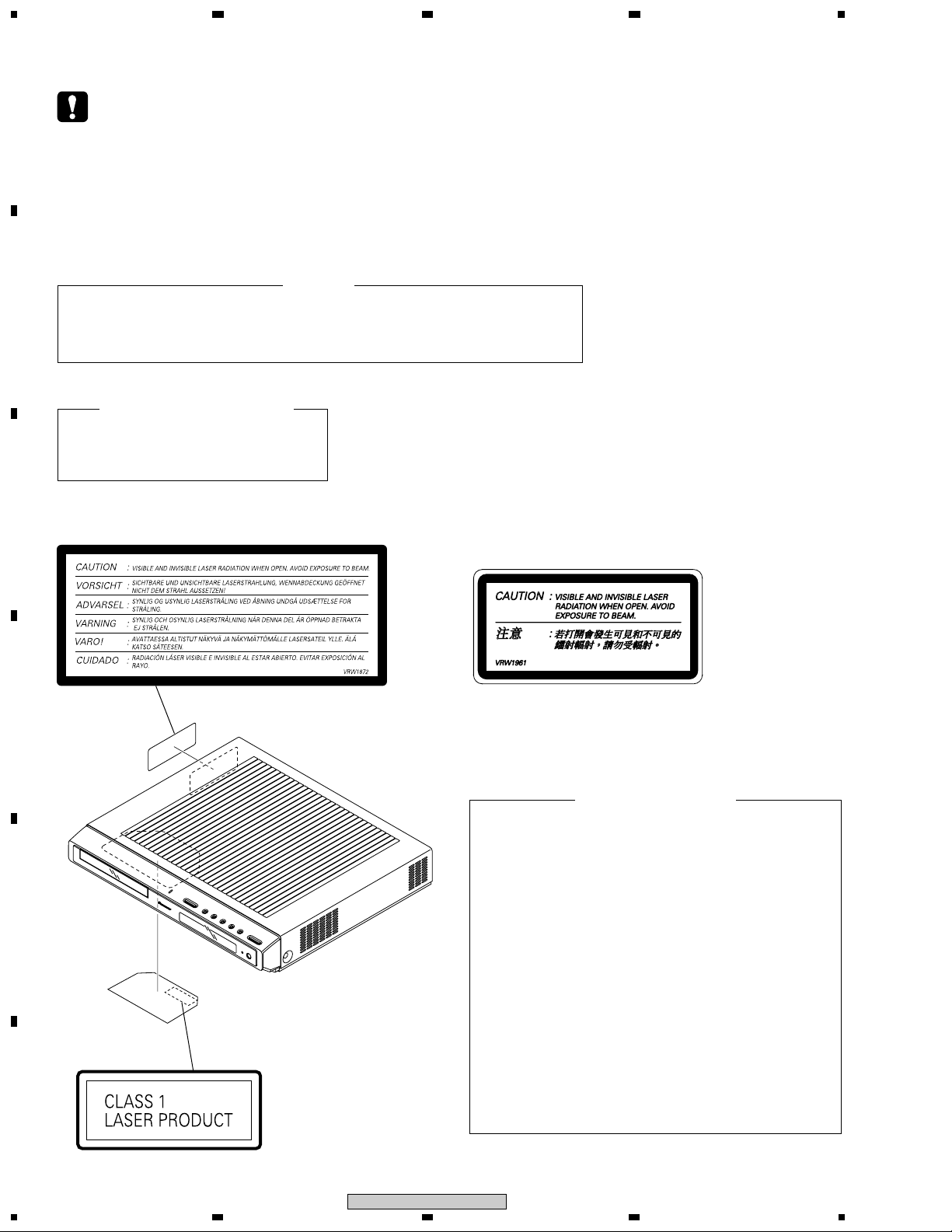
LABEL CHECK
VRW1872
(MLXJ/NC and YLXJ/NC Types)
VRW1961
(LFXJ Type)
D
Additional Laser Caution
1. Laser Interlock Mechanism
• Loading switch (S101 on the LOAB Assy) is used for interlock
mechanism of the laser.
When this switch turned ON in SW2 (CLOSE) side (OPEN signal is
0V and CLOSE signal is 3.5V), a laser becomes the status which can
completely oscillation.
Furthermore, the laser completely oscillates in the disc judgment and
E
Name Label
F
disc playback.
When player is power ON state and laser diode is not completely
oscillating, 780nm laser diode is always oscillating by half power.
• Laser diode is driving with Q201 (650nm LD) and Q211 (780nm LD)
on the DVDM Assy.
Therefore, when short-circuit between the emitter and collector of these
transistors or the base voltage is supplied for transistors turn on, the
laser oscillates. (failure mode)
• In the test mode ∗ , there is the mode that the laser oscillates except
for the disc judgment and playback. LD ON mode in the test mode
oscillates with the laser forcibly.
The interlock mechanism mentioned above becomes invalid in this
mode.
2. When the cover is open, close viewing through the objective lens with
the naked eye will cause exposure to the laser beam.
∗ : Refer to page 78 on the service manual RRV2946.
2
XV-DV424
1234
Page 3

1
jpfy
234
1. CONTRAST OF MISCELLANEOUS PARTS
NOTES:
CONTRAST TABLE
XV-DV424/LFXJ, MLXJ/NC, YLXJ/NC and XV-DV740/KUCXJ are constructed the same except for the following :
Parts marked by "NSP" are generally unavailable because they are not in our Master Spare Parts List.
The mark found on some component parts indicates the importance of the safety factor of the part.
Therefore, when replacing, be sure to use parts of identical designation.
Screws adjacent to mark on product are used for disassembly.
Reference Nos. indicate the pages and Nos. in the service manual for the base model.
For the applying amount of lubricants or glue, follow the instructions in this manual.
(In the case of no amount instructions, apply as you think it appropriate.)
When ordering resistors, first convert resistance values into code form as shown in the following examples.
•
Ex.1 When there are 2 effective digits (any digit apart from 0), such as 560 ohm and 47k ohm (tolerance is shown by J=5%,
and K=10%).
560 Ω→56 × 10
47k Ω→47 × 10
0.5 Ω→R50 ..................................................................................... RN2H
1 Ω→1R0 ..................................................................................... RS1P
Ex.2 When there are 3 effective digits (such as in high precision metal film resistors).
5.62k Ω→ 562 × 10
1
→ 561 ........................................................ RD1/4PU 5 6 1 J
3
→ 473 ........................................................ RD1/4PU 4 7 3 J
R 5 0
1 R 0
1
→ 5621 ...................................................... RN1/4PC 5 6 2 1 F
K
K
Part No.
No. Mark Symbol and Description XV-DV740 XV-DV424 XV-DV424 XV-DV424 Remarks
/KUCXJ /LFXJ /MLXJ/NC /YLXJ/NC
PCB ASSEMBLIES
P9- 5 CONTROL ASSY XWZ3882 XWZ3879 XWZ3879 XWZ3879
NSP MAIN ASSY XWM3253 XWM3250 XWM3250 XWM3250
A
B
C
P9- 8 POWER ASSY XWZ3885 XWZ3872 XWZ3871 XWZ3871
NSP COMPLEX ASSY XWM3256 XWM3247 XWM3246 XWM3246
PACKING SECTION
P7- 1 Power Cord ADG7021 ADG7098 ADG1154 ADG1154
P7- 8 Operating Instructions (English) XRB3037 XRB3036 XRB3036 XRB3036
P7-14 Operating Instructions (French) XRC3147 Not used Not used Not used
Operating Instructions (Chinese) Not used XRC3145 XRC3145 XRC3145
P7-17 Operating Instructions (English/French) XRE3084 Not used Not used Not used
Operating Instructions (English/Chinese) Not used XRE3085 XRE3085 XRE3085
P7-21 Packing Case XHD3433 XHD3436 XHD3434 XHD3434
P7-23 NSP Warranty Card ARY7045 Not used Not used Not used
EXTERIOR SECTION
P9- 4 FM/AM TUNER Unit AXX7172 AXX7173 AXX7173 AXX7173
P9-14 Power Transformer (AC110-120V) XTS3075 XTS3075 Not used Not used
P9-14 Power Transformer (AC220-230V) Not used Not used XTS3077 Not used
P9-14 Power Transformer (AC240V) Not used Not used Not used XTS3078
P9-15 Fuse (FU1 : 6.3A) REK1069 REK1069 Not used Not used
P9-15 Fuse (FU1 : T2.5A) Not used Not used REK1026 REK1026
P9-16 Fuse (FU2 : 6.3A) REK1069 REK1069 Not used Not used
P9-16 Fuse (FU2 : T5.0A) Not used Not used REK1029 REK1029
P9-24 Rear Panel XNC3298 XNC3303 XNC3300 XNC3301
P9-54 Name Label XAX3456 XAX3475 XAX3454 XAX3454
P9-55 NSP Fuse Card AAX2374 AAX2374 Not used Not used
P9-63 NSP Energy Star Label AAX8022 Not used Not used Not used
Push Rivet Not used Not used XEC3034 XEC3034 No. 1
Fan Barrier Not used Not used XMR3089 XMR3089 No. 2
Caution Label Not used VRW1961 VRW1872 VRW1872 *1
D
E
NSP SISIR Label Not used Not used XAX3469 Not used
NSP Black Label Not used XAX3394 Not used Not used
P11- 9 Front Panel XMB3155 XMB3165 XMB3165 XMB3165
P11-17 F.L Barrier XEC3055 Not used Not used Not used
FRONT SECTION
Notes : For PCB ASSEMBLIES, Refer to “CONTRAST OF PCB ASSEMBLIES”.
The numbers in the remarks column correspond to the numbers on the “ EXPLODED VIEWS ”.
*1 Refer to “LABEL CHECK”.
1
2
XV-DV424
3
F
3
4
Page 4

1
EXPLODED VIEWS
EXTERIOR SECTION
A
MLXJ/NC and YLXJ/NC types only
B
23
1
2
Rear Panel
4
C
CONTRAST OF PCB ASSEMBLIES
CONTROL ASSY
F
F
XWZ3879 and XWZ3882 are constructed the same except for the following :
Mark Symbol and Description
IC3003, IC3051–IC3053, IC3055–IC3058 BA4558F NJM4558MD
D
J
F
XWZ3872, XWZ3871 and XWZ3885 are constructed the same except for the following :
E
Mark Symbol and Description
C3176 CKSRYB123K50 CKSRYB153K50
C3179 CKSRYB563K16 CKSRYB104K16
C3183 CKSRYB183K25 CKSRYB273K16
C3184, C3185 Not used CKSRYB103K50
R3147 RS1/16S104J RS1/16S823J
R3184 RS1/16S682J RS1/16S822J
R5539 Not used RS1/16S473J
POWER ASSY
Q52 2SC4081 2SC4081 Not used
D55 UDZS20B UDZS20B Not used
T2 TRANSFORMER ATT7079 ATT7079 ATT7078
R1 (2.2MΩ/ 1/2W) RCN1080 Not used Not used
R55 RS1/16S222J RS1/16S222J Not used
XWZ3882 XWZ3879
XWZ3885 XWZ3872 XWZ3871
Part No.
Part No.
Remarks
Remarks
R56 RS1/16S223J RS1/16S223J Not used
AN1 1P AC INLET XKP3042 XKP3042 XKP3041
KN2 WRAPPING TERMINAL VNF1084 Not used Not used
F
4
1234
XV-DV424
 Loading...