

Pioneer XV-DV370, XV-DV368, XV-DV375K Service Manual
DVD/CD RECEIVER
XV-DV370
XV-DV368
XV-DV375K
THIS MANUAL IS APPLICABLE TO THE FOLLOWING MODEL(S) AND TYPE(S).
Model Type Power Requirement Region No. Remarks
XV-DV370 WYXJ5 AC 220 V to 240 V 2
XV-DV370 WVXJ5 AC 220 V to 240 V 2
XV-DV368 WYXJ5 AC 220 V to 240 V 2
XV-DV375K WXJ/RE5 AC 220 V to 240 V 5
ORDER NO.
RRV3607
¶ This service manual should be used together with the following manual(s):
Model No. Order No. Remarks
XV-DV363/WYXJ5 RRV3568
For SPECIFICATIONS and PANEL FACILITIES, refer to the operating instructions.
PIONEER CORPORATION 4-1, Meguro 1-chome, Meguro-ku, Tokyo 153-8654, Japan
PIONEER ELECTRONICS (USA) INC. P.O. Box 1760, Long Beach, CA 90801-1760, U.S.A.
PIONEER EUROPE NV Haven 1087, Keetberglaan 1, 9120 Melsele, Belgium
PIONEER ELECTRONICS ASIACENTRE PTE. LTD. 253 Alexandra Road, #04-01, Singapore 159936
PIONEER CORPORATION 2007
T – ZZK JUNE 2007 Printed in Japan
1
jpfy
23
1. CONTRAST OF MISCELLANEOUS PARTS
4
NOTES:
A
Parts marked by "NSP" are generally unavailable because they are not in our Master Spare Parts List.
The mark found on some component parts indicates the importance of the safety factor of the part.
Therefore, when replacing, be sure to use parts of identical designation.
Screws adjacent to mark on product are used for disassembly.
Reference Nos. indicate the pages and Nos. in the service manual for the base model.
For the applying amount of lubricants or glue, follow the instructions in this manual.
(In the case of no amount instructions, apply as you think it appropriate.)
When ordering resistors, first convert resistance values into code form as shown in the following examples.
•
Ex.1 When there are 2 effective digits (any digit apart from 0), such as 560 ohm and 47k ohm (tolerance is shown by J=5%,
and K=10%).
560 Ω→56 × 10
47k Ω→47 × 10
1
→ 561 ........................................................ RD1/4PU 5 6 1 J
3
→ 473 ........................................................ RD1/4PU 4 7 3 J
0.5 Ω→R50 ..................................................................................... RN2H R 5 0 K
B
CONTRAST TABLE
Ex.2 When there are 3 effective digits (such as in high precision metal film resistors).
1 Ω→1R0 ..................................................................................... RS1P
1
5.62k Ω→ 562 × 10
→ 5621 ...................................................... RN1/4PC 5 6 2 1 F
1 R 0
K
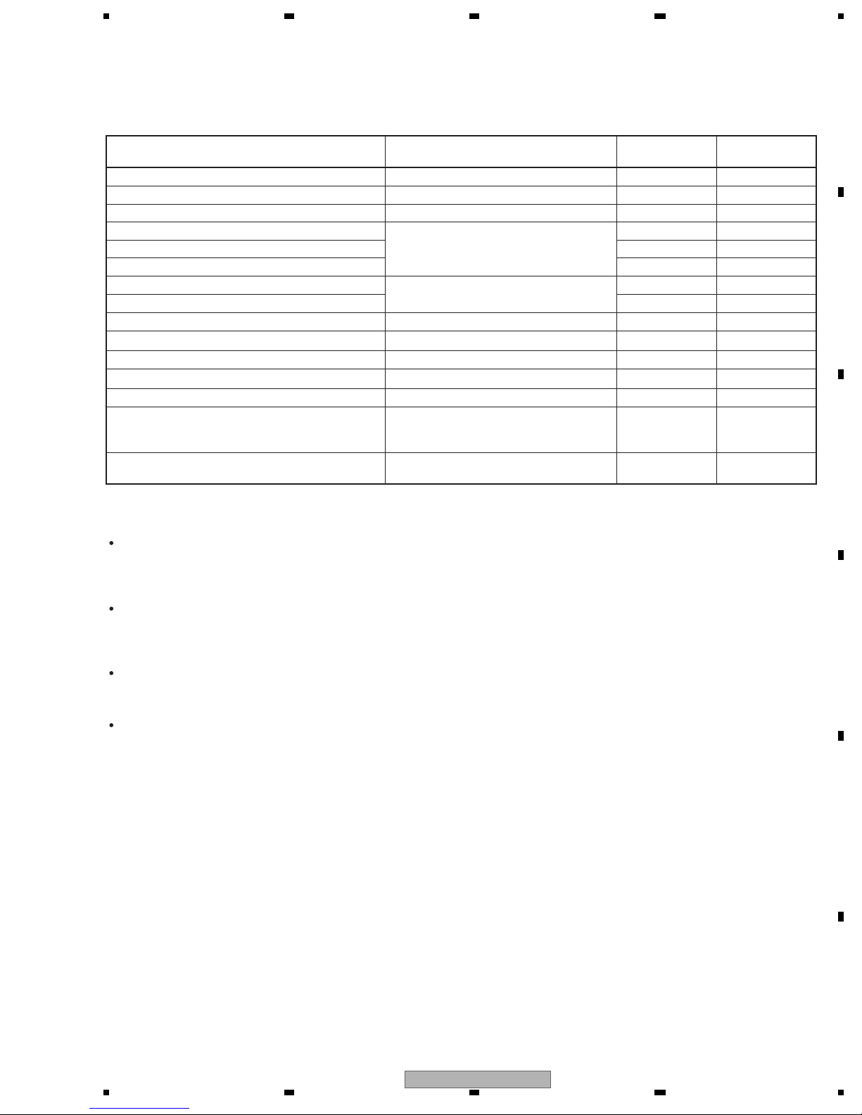
XV-DV370/WYXJ5, XV-DV370/WVXJ5, XV-DV368/WYXJ5, XV-DV375K/WXJ/RE5 and XV-DV363/WYXJ5 are constructed the same except for the following :
Ref.
Mark Symbol and Description XV-DV363 XV-DV370 XV-DV370 XV-DV368 XV-DV375K Remarks
No.
C
P51- 2 DVD MAIN Assy XWM3341 XWM3354 XWM3354 XWM3341 XWM3359
P51- 8 NSP MIC Assy Not used Not used Not used Not used XWM3375
PCB ASSEMBLIES
/WYXJ5 /WYXJ5 /WVXJ5 /WYXJ5 /WXJ/RE5
Part No.
*
P49- 1 > Power Cord ADG1127 ADG1127 ADG7108 ADG1127 ADG1127
P49- 5 Remote Control XXD3121 XXD3121 XXD3121 XXD3121 XXD3124
P49-10 Operating Instructions XRC3292 XRC3292 Not used Not used Not used
P49-11 Operating Instructions XRC3293 XRC3293 Not used Not used Not used
P49-12 Operating Instructions XRC3315 XRC3315 Not used Not used Not used
D
E
P49-13 Operating Instructions (Russian) Not used Not used Not used Not used XRC3294
P49-14 Setup Guide (English / French) XRC3281 XRC3309 Not used Not used Not used
P49-15 Setup Guide (German / Italian) XRC3282 XRC3310 Not used Not used Not used
P49-16 Setup Guide (Dutch / Spanish) XRC3283 XRC3311 Not used Not used Not used
P49-17 Setup Guide (Russian) Not used Not used Not used Not used XRC3302
P49-22 Packing Case XHD3704 XHD3733 XHD3733 XHD3732 XHD3746
P51-21 5P Flexible Cable/60V (J1907) Not used Not used Not used Not used XDD3232
P51-25 Rear Panel XNC3498 XNC3527 XNC3527 XNC3526 XNC3528
P51-27 Front Panel Assy XXG3328 XXG3331 XXG3331 XXG3330 XXG3324
P51-30 NSP Display Window XAK3590 XAK3590 XAK3590 XAK3590 XAK3575
P51-31 NSP Front Panel XMB3271 XMB3285 XMB3285 XMB3280 XMB3286
PACKING SECTION
(English / French)
(German / Italian)
(Dutch / Spanish)
Operating Instructions (English) Not used Not used XRB3081 Not used Not used
Operating Instructions Not used Not used Not used XRC3308 Not used
(Swedish / Norwegian)
Operating Instructions Not used Not used Not used XRC3316 Not used
(Finnish / Danish)
Setup Guide (English) Not used Not used XRB3080 Not used Not used
EXTERIOR SECTION
P51-36 MIC Knob Not used Not used Not used Not used AAK8309
P51-38 NSP Name Label XAL3260 XAL3284 XAL3284 XAL3283 XAL3285
Notes : For PCB ASSEMBLIES, Refer to “CONTRAST OF PCB ASSEMBLIES”.
F
2
* Refer to XV-DV365K/WXJ/RE5 on the Service manual RRV3568.
1234
XV-DV370
1
CONTRAST OF PCB ASSEMBLIES
DVD MAIN ASSY
B
F
234
XWM3354, XWM3359 and XWM3341 are constructed the same except for the following :
Mark Symbol and Description
IC3961 Not used Not used AK5358AET
D3961, D3962 Not used Not used UDZS3R9(B)
CN3961 CONNECTOR Not used Not used CKS3370
R249 Not used Not used RS1/16S330J
R3966 Not used Not used RS1/16S102J
R3967 Not used Not used RS1/16S332J
R3968 Not used Not used RS1/16S182J
R3969 Not used Not used RAB4C101J
R5502 Not used Not used RS1/16S104J
R5513 Not used Not used RD1/4PU153J
R5514 RD1/4PU683J RD1/4PU473J RD1/4PU473J
R5515 RD1/4PU473J RD1/4PU473J RD1/4PU823J
R5516 RD1/4PU153J Not used Not used
R5571 Not used Not used RS1/16S102J
C3961 Not used Not used CKSRYB105K16
C3962, C3966 Not used Not used CKSRYB104K16
C3963, C3965 Not used Not used CKSQYB225K10
C3967 Not used Not used CEAT220M25
C3968 Not used Not used CKSRYB103K50
* Refer to XV-DV365K/WXJ/RE5 on the Service manual RRV3568.
XWM3341 XWM3354 XWM3359
Part No.
Remarks
*
*
*
*
*
*
*
*
*
*
*
*
*
*
*
*
A
B
C
D
E
F
1
XV-DV370
2
3
4
3
XV-DV363
DVD/CD RECEIVER
XV-DV363
XV-DV365K
THIS MANUAL IS APPLICABLE TO THE FOLLOWING MODEL(S) AND TYPE(S).
ORDER NO.
RRV3568
Model Type Power Requirement
XV-DV363 WYXJ5 AC 220 V to 240 V 2
XV-DV365K WXJ/RE5 AC 220 V to 240 V 5
Regional restriction codes
(Region No.)
Remarks
For details, refer to "Important Check Points for good servicing".
PIONEER CORPORATION 4-1, Meguro 1-chome, Meguro-ku, Tokyo 153-8654, Japan
PIONEER ELECTRONICS (USA) INC. P.O. Box 1760, Long Beach, CA 90801-1760, U.S.A.
PIONEER EUROPE NV Haven 1087, Keetberglaan 1, 9120 Melsele, Belgium
PIONEER ELECTRONICS ASIACENTRE PTE. LTD. 253 Alexandra Road, #04-01, Singapore 159936
PIONEER CORPORATION 2007
T-IZK APR. 2007 printed in Japan
1234
SAFETY INFORMATION
A
This service manual is intended for qualified service technicians ; it is not meant for the casual doit-yourselfer. Qualified technicians have the necessary test equipment and tools, and have been
trained to properly and safely repair complex products such as those covered by this manual.
Improperly performed repairs can adversely affect the safety and reliability of the product and
may void the warranty. If you are not qualified to perform the repair of this product properly and
safely, you should not risk trying to do so and refer the repair to a qualified service technician.
B
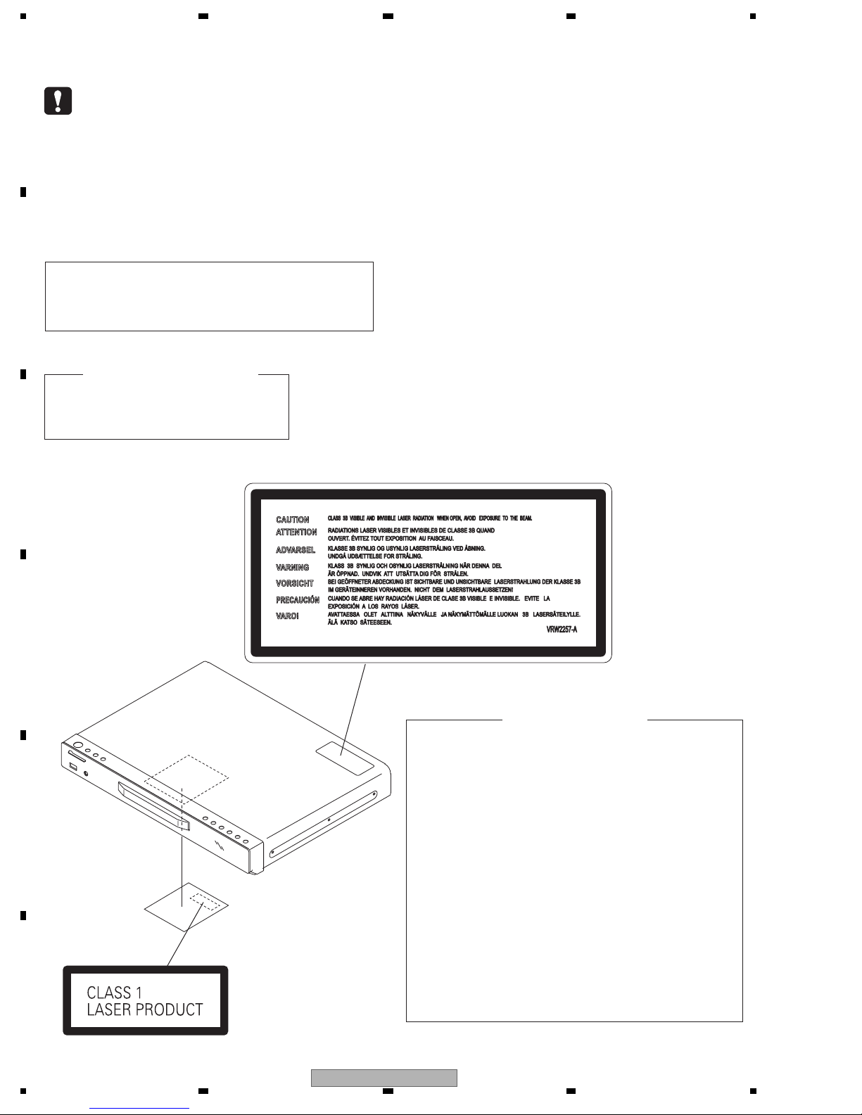
The laser component is capable of emitting radiation exceeding
WARNING!
the limit for CLASS 1. A specially instructed person should do
servicing operation of the apparatus.
LASER DIODE CHARACTERISTICS
FOR DVD : MAXIMUM OUTPUT POWER : 5 mW
WAVELENGTH : 650 nm
FOR CD : MAXIMUM OUTPUT POWER : 7 mW
WAVELENGTH : 780 nm
C
LABEL CHECK
D
VRW2257
E
Name Label
F
2
1 234
Additional Laser Caution
1. Laser Interlock Mechanism
• Loading switch (S101 on the LOAB Assy) is used for interlock
mechanism of the laser.
When this switch turned ON in SW2 (CLOSE) side (OPEN signal is
0 V and CLOSE signal is 3.5 V), a laser becomes the status which
can completely oscillation.
Furthermore, the laser completely oscillates in the disc judgment and
disc playback.
When player is power ON state and laser diode is not completely
oscillating, 780 nm laser diode is always oscillating by half power.
• Laser diode is driving with Q307 (650 nm LD) and Q308 (780 nm
LD) on the DVD MAIN Assy.
Therefore, when short-circuit between the emitter and collector of these
transistors or the base voltage is supplied for transistors turn on, the
laser oscillates. (failure mode)
• In the test mode ∗ , there is the mode that the laser oscillates except
for the disc judgment and playback. LD ON mode in the test mode
oscillates with the laser forcibly.
The interlock mechanism mentioned above becomes invalid in this
mode.
2. When the cover is open, close viewing through the objective lens with
the naked eye will cause exposure to the laser beam.
∗ : Refer to page 25.
XV-DV363
5678
A
B
C
D
E
56
XV-DV363
F
3
7
8

1234
CONTENTS
SAFETY INFORMATION..................................................................................................................................... 2
1. SERVICE PRECAUTIONS............................................................................................................................... 5
A
B
C
D
E
1.1 NOTES ON SOLDERING .......................................................................................................................... 5
1.2 CAUTION................................................................................................................................................... 5
2. SPECIFICATIONS............................................................................................................................................ 6
2.1 SPECIFICATIONS and ACCESORRIES ................................................................................................... 6
2.2 PANEL FACILITIES.................................................................................................................................... 7
3. BASIC ITEMS FOR SERVICE........................................................................................................................ 10
3.1 CHECK POINTS AFTER SERVICING..................................................................................................... 10
3.2 PCB LOCATIONS .....................................................................................................................................11
3.3 JIGS LIST ................................................................................................................................................ 12
3.4 CLEANING............................................................................................................................................... 12
4. BLOCK DIAGRAM.......................................................................................................................................... 14
4.1 OVERALL WIRING CONNECTION DIAGRAM and LOAB ASSY ........................................................... 14
4.2 OVERALL BLOCK DIAGRAM.................................................................................................................. 16
5. DIAGNOSIS.................................................................................................................................................... 18
5.1 METHOD FOR DIAGNOSING DEGRADATION OF THE LDS ON THE PICKUP................................... 18
5.2 DVD TROUBLE SHOOTING ................................................................................................................... 19
5.3 CIRCUIT DESCRIPTION OF DIGITAL AMP. SECTION .......................................................................... 22
5.4 SPECIFICATIONS FOR THE PROTECTION CIRCUITS FOR THE DIGITAL AMPLIFIER..................... 23
5.5 PASS/FAIL TEST PROCEDURE OF HDMI TRANSMITTER IC.............................................................. 24
6. SERVICE MODE ............................................................................................................................................ 25
6.1 TEST MODE............................................................................................................................................ 25
6.2 DISPLAY SPECIFICATION OF THE TEST MODE.................................................................................. 26
6.3 FUNCTIONAL SPECIFICATION OF THE SHORTCUT KEY .................................................................. 27
6.4 SPECIFICATION OF MODEL INFORMATION DISPLAY ........................................................................ 28
6.5 FUNCTIONAL SPECIFICATION OF THE SERVICE MODE................................................................... 29
6.6 SERVICE TEST MODE ........................................................................................................................... 30
7. DISASSEMBLY .............................................................................................................................................. 33
8. EACH SETTING AND ADJUSTMENT ........................................................................................................... 40
8.1 ADJUSTMENT......................................................................................................................................... 40
8.2 ID NUMBER AND ID DATA SETTING ..................................................................................................... 45
9. EXPLODED VIEWS AND PARTS LIST.......................................................................................................... 48
9.1 PACKING SECTION ................................................................................................................................ 48
9.2 EXTERIOR SECTION.............................................................................................................................. 50
9.3 06 LOADER ASSY................................................................................................................................... 52
9.4 TRAVERSE MECHANISM ASSY-S ......................................................................................................... 54
10. SCHEMATIC DIAGRAM............................................................................................................................... 56
10.1 DVD MAIN ASSY (1/5) .......................................................................................................................... 56
10.2 DVD MAIN ASSY (2/5) .......................................................................................................................... 58
10.3 DVD MAIN ASSY (3/5) .......................................................................................................................... 60
10.4 DVD MAIN ASSY (4/5) .......................................................................................................................... 62
10.5 DVD MAIN ASSY (5/5) .......................................................................................................................... 64
10.6 DAMP ASSY (1/2).................................................................................................................................. 66
10.7 DAMP ASSY (2/2).................................................................................................................................. 68
10.8 DISPLAY, USB, LED and KEY ASSYS .................................................................................................. 70
10.9 MIC ASSY (XV-DV365K ONLY)............................................................................................................. 72
10.10 EUROSCART ASSY............................................................................................................................ 74
10.11 POWER SUPPLY UNIT ....................................................................................................................... 76
10.12 WAVEFORMS ...................................................................................................................................... 78
11. PCB CONNECTION DIAGRAM.................................................................................................................... 80
11.1 LOAB ASSY ........................................................................................................................................... 80
11.2 MIC ASSY (XV-DV365K ONLY)............................................................................................................. 81
11.3 DVD MAIN ASSY ................................................................................................................................... 82
11.4 DAMP ASSY .......................................................................................................................................... 86
11.5 DISPLAY, USB, LED and KEY ASSYS ...........................................................................................
11.6 POWER SUPPLY UNIT ......................................................................................................................... 90
11.7 EUROSCART ASSY .............................................................................................................................. 92
12. PCB PARTS LIST......................................................................................................................................... 93
....... 88
F
4
1 234
XV-DV363

5678
1. SERVICE PRECAUTIONS
1.1 NOTES ON SOLDERING
• For environmental protection, lead-free solder is used on the printed circuit boards mounted in this unit.
Be sure to use lead-free solder and a soldering iron that can meet specifications for use with lead-free solders for repairs
accompanied by reworking of soldering.
• Compared with conventional eutectic solders, lead-free solders have higher melting points, by approximately 40 °C.
Therefore, for lead-free soldering, the tip temperature of a soldering iron must be set to around 373 °C in general, although
the temperature depends on the heat capacity of the PC board on which reworking is required and the weight of the tip of
the soldering iron.
Do NOT use a soldering iron whose tip temperature cannot be controlled.
Compared with eutectic solders, lead-free solders have higher bond strengths but slower wetting times and higher melting
temperatures (hard to melt/easy to harden).
The following lead-free solders are available as service parts:
• Parts numbers of lead-free solder:
GYP1006 1.0 in dia.
GYP1007 0.6 in dia.
GYP1008 0.3 in dia.
1.2 CAUTION
A
B
C
NOTES ON BTL DRIVE
As a signal to drive the BTL is output from the negative speaker terminal, DO NOT short-circuit between the
negative speaker terminal and ground, such as the chassis.
Do not short-circuit between the plus speaker terminal and ground, such as the chassis, too.
Negative Speaker Terminal
Do not short-circuit
Ground (Chassis)
D
E
56
XV-DV363
F
5
7
8
1234
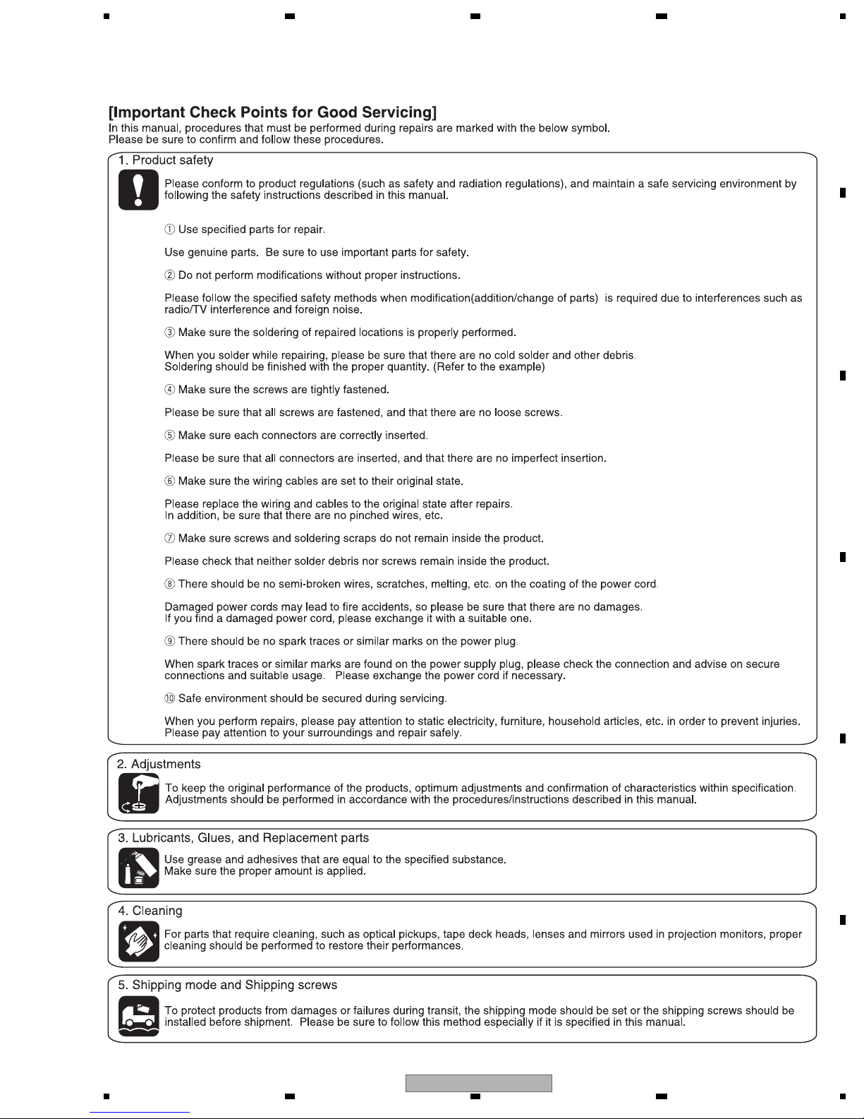
2. SPECIFICATIONS
2.1 SPECIFICATIONS and ACCESORRIES
A
B
C
(XV-DV363)
(XV-DV365K)
D
Accessories
• Power Cord (ADG1127) • FM Antenna (ADH7030) • Video Cable
E
(L = 1.5 m) (XDE3046)
• Remote Control
(XV-DV363 : XXD3121)
(XV-DV365K : XXD3124)
• AM Loop Antenna
(ATB7013)
F
6
1 234
• Dry Cell Battery (AA/R6)
XV-DV363
5678
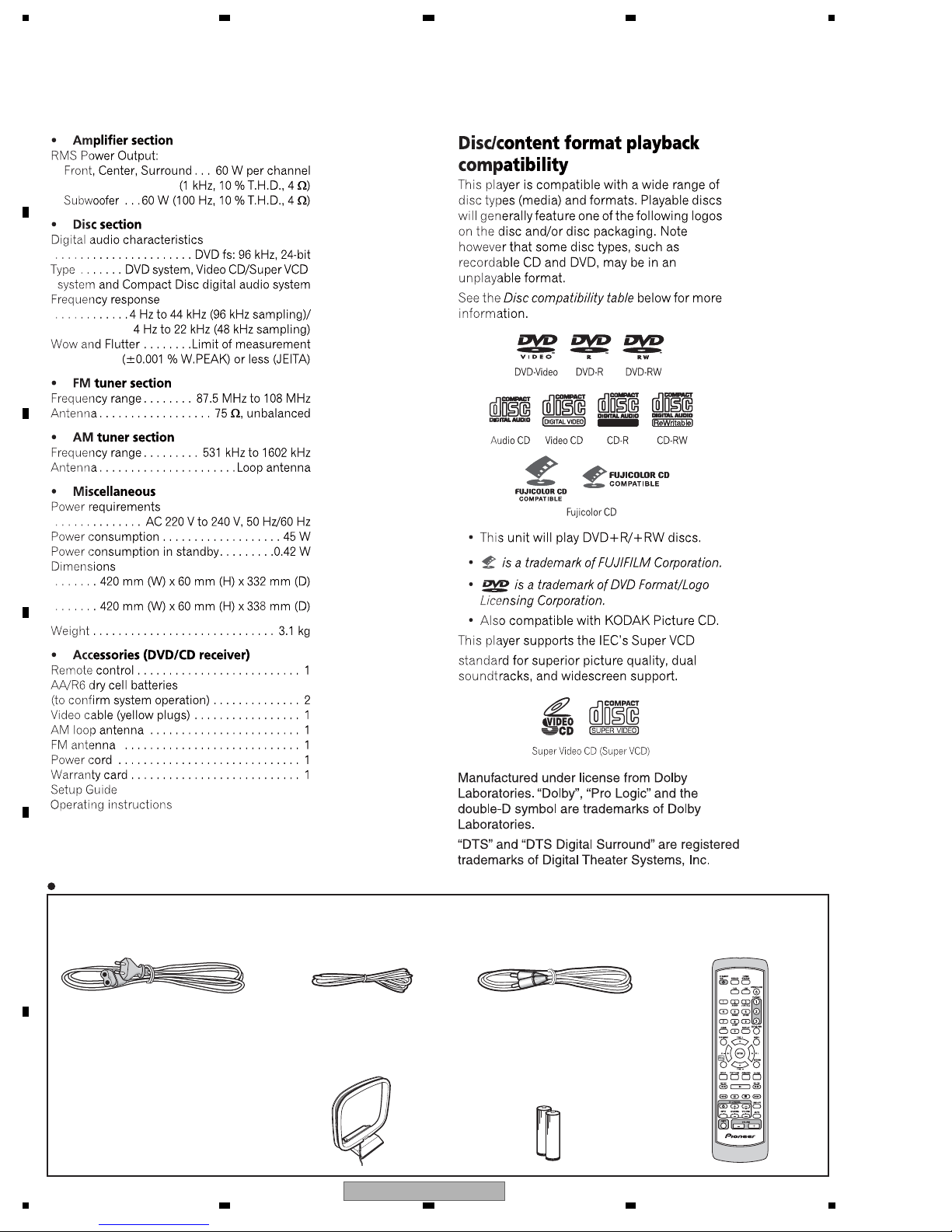
2.2 PANEL FACILITIES
Front panel
A
B
C
XV-DV363
XV-DV365K
PHONESUSB SUB MIC MAIN MIN VOL MAX
MIC
D
E
56
XV-DV363
F
7
7
8
A
Display
B
1234
C
D
E
F
8
1 234
XV-DV363
5678
Remote control
ECHO
KARAOKE
(XV-DV356K)
SHIFT+KARAOKE
SHIFT+ECHO
SHIFT+ SHIFT+
A
B
C
D
E
F
56
XV-DV363
9
7
8
1234
3. BASIC ITEMS FOR SERVICE
3.1 CHECK POINTS AFTER SERVICING
A
Check points after servicing (HTZ and system audio)
To keep the product quality after servicing, confirm recommended check points shown below.
No. Procedures Check points
1 Confirm the firmware version on Service Mode.
Confirm whether the customer complain has been solved. If the
2
customer complain occurs with the specific disc, use it for the
operation check.
Confirm playback error rates at the innermost and outermost
3
B
tracks by using the following disc.
DVD test disc (GGV1025)
4 Play back a CD. (track search) Audio and operations must be normal.
Play back a DVD.
5
(Menu operation, Title/chapter search)
6 Check the tuner (AM and FM) operations. Audio and operations must be normal.
7 Check the sound from headphone output. Sound must be normal, without noise.
8 Check the appearance of the product.
The version of the firmware must be latest.
Update firmware to the latest one, if it is not the latest.
The customer complain must not be reappeared.
Video, audio and operations must be normal.
The error rates must be less than 5.0e-4.
Video, audio and operations must be normal.
No scratches or dirt on its appearance after receiving it for
service.
C
See the table below for the items to be checked regarding video and audio:
Item to be checked regarding video Item to be checked regarding audio
Block noise Distortion
Horizontal noise Noise
Dot noise Volume too low
Disturbed image (video jumpiness) Volume too high
Too dark Volume fluctuating
Too bright Sound interrupted
D
Mottled color
E
F
10
1 234
XV-DV363
5678
3.2 PCB LOCATIONS
E
USB Assy
J
POWER SUPPLY Unit
H
MIC Assy
(XV-DV365K only)
C
DAMP Assy
06 LOADER Assy
I
EUROSCART Assy
A
LOAB Assy
FM/AM TUNER Unit
B
DVD MAIN Assy
D
DISPLAY Assy
A
B
C
Front panel section
G
KEY Assy
Mark No. Description Part No.
LIST OF ASSEMBLIES
NSP 1..06 LOADER ASSY VWT1226
2..LOAB ASSY VWG2346
1..DAMP ASSY XWK3318
1..DVD MAIN ASSY (XV-DV363) XWM3341
1..DVD MAIN ASSY (XV-DV365K) XWM3342
NSP 1..COMPLEX ASSY XWM3372
2..DISPLAY ASSY XWZ4256
2..USB ASSY XWZ4259
2..KEY ASSY XWZ4261
2..LED ASSY XWZ4263
NSP 1..JACK ASSY AWM8034
2..EUROSCART ASSY AWU8291
Bottom view
F
LED Assy
Rear view
Mark No. Description Part No.
1..MIC ASSY (XV-DV365K ONLY) XWM3375
> 1..POWER SUPPLY UNIT XWR3012
1..FM/AM TUNER UNIT AXX7248
D
E
F
56
XV-DV363
11
7
8
1234
3.3 JIGS LIST
Jigs list
A
Name Jig No. Remarks
Service Remote Control Unit GGF1381
DVD Test Disc (DVD-Video) GGV1025
CD Test Disc STD-905 Check of CD
DVD Data Disc GGV1269 ID data setting
Speaker Cable with terminal SDS1174 (FL/WHITE)
SDS1175 (FR/RED), SDS1176 (SL/BLUE)
SDS1177 (SR/GRAY), SDS1178 (C/GREEN)
B
Lubricants and Glues list
Name Lubricants and Glues No. Remarks
Lubricating Oil GYA1001
Daifree
C
GEM1036
GEM1037Silicone Adhesive
GYL1001Screw tight
adjustment, diagnosis
Check of DVD-Video
For checking audio at the SP terminal
refer to "9.3 06 LOADER ASSY"
refer to "9.3 06 LOADER ASSY"
refer to "9.4 TRAVERSE MECHANISM ASSY-S"
refer to "8.1.5 MECHANISM ADJUSTMENT"
3.4 CLEANING
D
CLEANING
Before shipping out the product, be sure to clean the following positions by using the prescribed cleaning tools:
Position to be cleaned Cleaning tools
Pickup leneses Cleaning liquid : GEM1004
Cleaning paper : GED-008
E
F
12
1 234
XV-DV363

5678
A
B
C
D
E
56
XV-DV363
F
13
7
8
1234
4. BLOCK DIAGRAM
4.1 OVERALL WIRING CONNECTION DIAGRAM and LOAB ASSY
A
FM/AM
K
TUNER UNIT
(AXX7248)
No schematic Diagram
FM
AM
B
CN1
CE
DI
CLK
DO
GND
TXL
+9V
TXR
VSM
RDS
GND
11P FFC
(ADD7543)
CN5701
CKS3376-
CE
1
2
DI
CLK
3
4
DO
GND
5
TXL
6
+9V
7
TXR
8
VSM
9
RDS
10
GND
11
B B B( 1/5- 5/5)
DVD MAIN ASSY
(XWM3341:XV-DV363/WYXJ5)
(XWM3342:XV-DV365K/WXJ/RE5)
C
D
E
F
7
6
2
3
JA3921
4
5
AKN7003
1
1
2
JA3922
3
RKN1004
AC POWER CORD
MIC ASSY
H
(XWM3375
:
ECHOCONT
XV-DV365K/WXJ/RE5
J
POWER
SUPPLY UNIT
(XWR3012)
CN1
LIVE
2
NEUTRAL
1
CN3 CN1001
B13B-PH-K-S B13B-PH-K-S
AC_DET
SW10.5V
EV5.0V
SW5.0V
SW6.8V
GND
SW3.3V(B)
SW3.3V(A)
Pwr-ctr
GND
FL DC-
FL DC+
-25.5V
GND
+B
2
1
B2P-VH
CN2
CN3921 CN5702
1
MIC SW
2
3
V+10V
4
5P FFC
MIC
GND
(XDD3232-)
5
)
PG13KK-F22
1
2
3
4
5
6
7
8
9
10
11
12
13
CKS3370
2
4
1
3
5
1
2
3
4
5
6
7
8
9
10
11
12
13
MIC SW
ECHOCONT
V+10V
MIC
GND
AC_DET
SW10.5V
EV5.0V
SW5.0V
SW6.8V
GND
SW3.3V(B)
SW3.3V(A)
Pwr-ctr
GND
FL DC-
FL DC+
-25.5V
GNDD
VS(VREF)
SW(DVD/CD)
VR650
VRCOM
VR780
GNDD
LD(780)
LD(650)
GNDD
VSHF
TRKG DRV
TRKG RTN
FOCS DRV
FOCS RTN
CN101
VKN2045
F
VCC
E
D
C
RF
B
A
PD
DVD LOADER
CN1
OKN8001
(ADD7545-)
24P FFC
GNDD
F
VS(VREF)
VCC
E
D
C
SW(DVD/CD)
RF
B
A
VR650
VRCOM
VR780
GNDD
LD(780)
PD
LD(650)
GNDD
VSHF
TRKG DRV
TRKG RTN
FOCS DRV
FOCS RTN
PICK UP ASSY
OWY8087-
TRAVERSE MECHA ASSY
1
2
3
4
5
6
7
8
9
10
11
12
13
14
15
16
17
18
19
20
21
22
23
24
DXB1860-
VWT1226-
CN602
2
1
A
LOAB ASSY
(VWG2346)
CN102
VKN1243
12P FFC
4P FFC
PF05PP-B40
12
INSIDE
11
10
V
9
U
8
HB
7
W-
6
W+
5
V-
4
V+
3
U-
2
U+
1
V+5S
CN103
VKN1235
1
ST2-(~B~)
2
ST2+(B)
3
ST1-(~A~)
4
1
LOAD-
LOAD+
3
SW2
4
GNDD
SW1
INSIDE
WW
V
U
HB
W-
W+
SPINDLE MOTOR
V-
V+
U-
U+
V+5S
ST2-(~B~)
ST2+(B)
ST1+(A) ST1+(A)
ST1-(~A~)
STEPPING MOTOR
CN601 CN104
S5B-PH-K-S B5B-PH-K-S
LOAD-
1
LOAD+
22
SW2
3
4
GNDD
55
SW1
14
1 234
ADX7480-
XV-DV363
5678
CKS3378-
CN5602
CKS3378-
CN5901
IC5902
Vcc
GND
Vout
GP1UM27XKOVF
CN3101CN3001
AKP7199- AKM7077-
PCON
19
XHPSEL
18
HPL
17
GND
16
HPR
15
GND
14
3.3V
13
XRST
XPDN
111211
XMUTE
10
GND
9
SDA
8
SCL
7
GND
6
XOTW
5
XSD
4
SROUT
3
POWER
22
PLCCONT PLCCONT
11
CN3002 CN3102
AKP7199- AKM7077-
SD ATA1
19
SD ATA2
18
SD ATA3
17
GND
16
MCLK
15
GND
14
SCLK
13
LRCLK
12
GND
11
LIN1_L
10
GND
9
LIN1_R
8
GND
RECMUTE
SD ATA4
7
6
GND
5
4
3
2
GND
S_TVOUT_L
S_TVOUT_R
PCON
19
XHPSEL
18
HPL
17
GND
16
HPR
15
GND
14
3.3V
13
XRST
12
XPDN
XMUTE
10
GND
9
SDA
8
SCL
7
GND
6
XOTW
5
XSD
4
SROUT
3
POWER
SDATA1
19
SDATA2
18
SDATA3
17
GND
16
MCLK
15
GND
14
SCLK
13
LRCLK
12
GND
11
LIN1_L
10
GND
9
LIN1_R
8
GND
7
S_TVOUT_L
6
GND
5
S_TVOUT_R
4
RECMUTE
3
GND
2
SDATA4
11
VE+5
FLDATA
FLCK
FLCS
REMOCON
13 11
10
82
12
13P FFC(ADD7541)
4
6
321
5
VE+5
FLCS
FLCK
FLDATA
REMOCON
DISPLAY ASSY
(XWZ4256)
D
AAV7104(AAV7107)
VFDP
FLDC-
FLDC+
513
79
64
79
VFDP
FLDC-
FLDC+
FL
GND
CN3201
2
1
GNDD
108
GNDD
+B
GNDD
GNDD
F
KEY1
KEY1
B2P-VH
KEY2
12
1311
KEY2
HDMI OUTPUT
12
AKP7210-
(AKP7211)
CN931
KEY2A
KEY2A
G
KEY ASSY
(XWZ4261)
V+10V
312
3P FFC
(XDD3229-)
V+10V
LED ASSY
(XWZ4263)
GA UPPER
EU,RUSSIA,KUC & J
21654
DATA2+
8
10
7
3
DATA2 SHIELD
KEY2A
GND
911 17
DATA0-
DATA1-
DATA2-
DATA0+
DATA1+
CN5908 CN5907
GND
KEY1 KEY1
LED
V+10
LED
CLOCK+
DATA0 SHIELD
DATA1 SHIELD
CKS3370 CKS3370
1
2
3
44
5P FFC (XDD3231)
55
CN5909
312
LED
CKS3368 CKS3368
GND
CN5603
SLR-343BBT
NC
CEC
CLOCK-
HDMISCL
CLOCK SHIELD
15p:CKS3380
GNDD
HP_L
HPMUTE
315971311
CN5601
246810
2
214
13
CN5906
HP_L
GNDD
HPMUTE
15p:CKS3380
KEY2A
1
GND
2
3
LED
V+10
4969787861310
C C C( 1/2- 2/2)
(XWK3318)
RKN1004
1815161314
HDMISDA
DDC/CEC GND
HP_DET
HP_R
553
HP_R
HP_DET
19
+5V
HOT PLUG DETECT
GNDUSB
V5USB
V5USB
15P FFC (XDD3234)
V5USB
V5USB
GNDUSB
E
DVDPOWER
USB_DP2
USB_DM2
10
11
USB_DP2
USB_DM2
VSEL1
SQEEZE
TVOUT_R
TVOUT_L
TVMUTE
SCART_R
SCART_L
VSEL2
GNDUSB
12
12
12
GNDUSB
USB ASSY
(XWZ4259)
DAMP ASSY
11
2
V+10
4
GND
6
8
GND
10 10
V+5
12
B
GND
14
G
GND
R
18
S_C
20
GND
V
GND
22
S_Y
CN451 CN461
CKS3388-
KEY1
KEY2
LED
V+10
15
14
14
15
1311
LED
V+10
KEY2
KEY1
2
3
3
4
55
6
7
7
8
9
9
11
11
(ADD7544)
12
13
13
14 11
151615
23P FFC
16
17
17
18
19
19
20
21
21
22
2323
CKS3388-
VSEL1
SQEEZE
V+10
TVOUT_R
GND
TVOUT_L
TVMUTE
SCART_R
GND
SCART_L
V+5
VSEL2
B
EURO SCART
GND
ASSY
G
GND
(AWU8291)
R
DVDPOWER
S_C
GND
V
GND
S_Y
I
HEAD PHONE
JA451
XKB3054-
EURO CONNECTOR
1
2
3
4
5
6
7
8
9
10
12
13
14
15
16
17
18
19
20
21
JA403
XKB3060-
(VKB1122)
V
JA5902
AKN7003-
USB
TVIN_L
TVIN_R
LINEOUT_L
LINEOUT_R
CN3111
AKB7114
CN3211
AKE7121
FR+
1
FR-
2
RR+
3
RR-
4
5
FL+
6
FL-
7
RL+
8
RL-
9
C+
10
C-
11
SW+
12
SW-
R OUT
R IN
L OUT
GND
GND
L IN
B
SQUEEZE
GND
NC
G
NC
GND
GND
R/C
BLANK
GND
GND
V/Y
NC
GND
COMPOSITE
VIDEO
OUTPUT
HP OUT
JA602
XKP3086
AUDIO
IN/OUT
6ch SP OUT
A
B
C
D
E
F
56
SR OUT
XV-DV363
15
7
8
1234
M
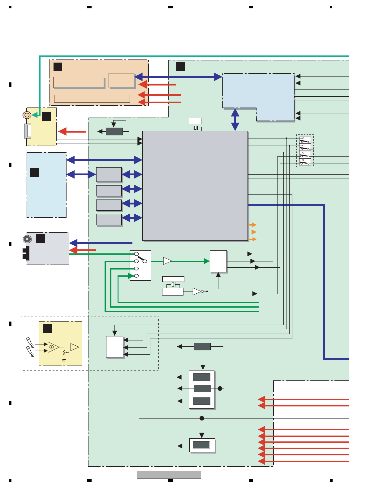
4.2 OVERALL BLOCK DIAGRAM
A
D
DISPLAY ASSY
5V
MOTOR
DRIVER
64M
SDRAM
16M
FLASH
64k
EEPROM
Display
Driver
USB POWER
FL
KEY
E
B
HP
USB
USB
ASSY
V+5USB
USB DP
USB DM
A
LOAB ASSY
C
LOADER
MECHA
K
FM/AM
TUNER
UNIT
D
+9V
TUNER
SCART
LINE/TV
MCACC
V+6R8
FL DC+/-
VFDP
• AUDIO PROCESSING
• Audio Decode
• Bass Management
• Virtual Surround
• Preset EQ
etc.
12.288M
74HCU04
B
DVD MAIN ASSY
VE+5
27M
BE
MT1389
AK5358AET
A/D
ADMCK0
G,B,R
Y, C
ADBCK
ADLRCK
ADDATA
ADMCK1
V
SYSTEM
UCOM
ACLK
ALRCK
MCLK
ASDAT0
ASDAT1
ASDAT2
MCDATA
PCON (from SMPS or D-A
DC DET
SCL
SDA
MUTE
RESET
PDN
SD
OTW
BCKO
LRCKO
MCKO
DATAO
XV-DV365K/WXJ/RE55
ONLY
MCLK
H
MIC ASSY
A/D
AK5358AET
E
F
16
1 234
ACLK
ALRCK
MCDATA
PWRCONT
+9V
V+1R8
V+5
XV-DV363
9V
DVD POWER
SW
SW
1.8V
SW
SW+10.5V
SW5.0VV+5V
SW3.3V(A)V+3
VE+5
V+10
VE+5
V+6R8
V+3R3
MCACC
LINE
SCART
5678
A
PCON (from SMPS or D-AMP)
DC DET
SCL
SDA
MUTE
RESET
PDN
SD
OTW
C
DAMP ASSY
MODULATER
TAS5508BPAG
LINE
SCART
MCACC
+3.3V
HP SEL
PWMA P
PWMA M
RESET
SD
PWMB P
PWMB M
ch7 ch8 PWM
TAS5122DCA
LPF
HP AMP
DRIVER
FRONT L
FRONT R
CENTER
SUB WOOFER
REAR L
REAR R
LINE OUT
LINE IN
SR OUT
MCACC MIC
B
C
FLDC +/-
VFDP
SW10.5V
FV5.0V
SW 5.0V
SW 6.8V
SW
SW
G, B, R
V
Y, C
Video
AMP
V+3
V+1R8
+B
J
POWER SUPPLY UNIT
V
Y, C
G, B, R
Y, C
V
HDMI
Transmitter
Scart
Circuit
TX
SCART (EU)
I
EUROSCART
ASSY
Composite
HDMI OUT
AC IN
D
E
F
56
XV-DV363
17
7
8
1234
5. DIAGNOSIS
5.1 METHOD FOR DIAGNOSING DEGRADATION OF THE LDS ON THE PICKUP
A
Case when this diagnosis is required :
When playback of any disc, including a test disc (DVD: GGV1025, CD: STD-905), won't play or doesn't play
How to diagnose
In the case mentioned above, degradation of the laser diodes (LDs) mounted on the 06SD Pickup Assy-S is suspected.
Measure the voltage between the two ends of one of the resistors mentioned below.
B
Measure the voltage between the both ends of R322 or R325 on the DVD MAIN
Assy. If the voltage is 0.4 V or higher, the 650-nm LD is degraded.
No playback of a CD :
No playback of a DVD :
Measure the voltage between the both ends of R321 or R326 on the DVD MAIN
Assy. If the voltage is 0.4 V or higher, the 780-nm LD is degraded.
C
PICKUP ASSY
D
CN101
XWM
If the measurements show degradation
of an LD, replace the 06SD Pickup
Assy-S.
DVD MAIN ASSY
B
SIDE
CONTACT
15
C771
L308
L309
4
ICT
R325
R326
1
0
1
0
1
0
1
0
1
12
E
R134
R135
C145
F
Q304
CONTACT
SIDE
C144
R314
24
R136
C146
R315
23
C133
C161
R318
13
R313
23
C131
R372
54
R371
C132
C781
R375 R373
Q305
C371
R374
C374
C373
2
C372
C772
CN101
1
C773R772
3
45
IC771
R771
L772
1
1
18
1 234
Q307
Q308
R321
FC1
R322
CN5601
C320
R310
R1001
B1
C309
C310
[CN5603]
XV-DV363
Front side
SIDE A
5678
5.2 DVD TROUBLE SHOOTING
No. Symptoms Diagnosis Contents Possible Defective Points
1 The power is not turned on. Are wires of output connector (POWER SUPPLY Unit) and CN1001
(DVD MAIN Assy) disconnected or damaged ?
Check that the following voltage is output :
Q1202-source on the DVD MAIN Assy: 3.3V
An opening screen is not
2
displayed on the monitor
(The FL display lights. The
mechanism does not work.)
Are the signals output from IC201-pin 97 (MDATA) and pin 98 (SCLK)
on the DVD MAIN Assy ? (in the range of 0-3V)
Are the signals input into IC5501-pin 50 (MDATA) and pin 51 (SCLK) on
the DVD MAIN Assy ? (in the range of 0-3V)
Check that the following voltage are output :
Q1302-collector on the DVD MAIN Assy: 5V
Connector / cable
POWER SUPPLY Unit
DVD MAIN Assy
DVD IC (IC201)
DVD MAIN Assy
UCOM (IC5501)
DVD MAIN Assy
5V Regulator IC (IC751)
A
B
Is a resonator (X201: 27MHz) on the DVD MAIN Assy oscillating ?
•
Is a signal input into IC203-pin26 (PCE#) on the DVD MAIN Assy ?
(Is a signal "H" for 80 mS and then "L" after the power is turned on ?)
-> Communication with flash ROM.
• Are the signals input into IC202-pin 16 (DWE#), pin 19 (DCS#)
and pin 38 (SDCLK) on the DVD MAIN Assy ?
(Is a signal fluctuating ?)
-> Communication with SDRAM
Is a signal output from IC203-pin 28 (PRD#) on the DVD MAIN Assy?
(Is a signal fluctuating for several hundred mS after the power is turned
on ?)
Is a signal input into IC5501-pin 67 (DVD ACK) on the DVD MAIN
Assy ? (Is a signal fluctuating ?)
-> Communication with FL Control IC
Is a signal output from IC5501-pin 78 (XREADY) on the DVD MAIN
Assy ? (Is a signal fluctuating in the range of 0-5V ?)
Are the signals output from IC5501-pin 49 (SDATA) on the DVD MAIN
Assy ? (in the range of 0-5V)
Are the signals of IC204-pin 5 (SDA) and pin 6 (SCL) on the DVD MAIN
Assy fluctuating for one or two seconds after the power is turned?
DVD MAIN Assy
Crystal resonator (X201)
DVD IC (IC201)
DVD MAIN Assy
DVD IC (IC201)
Flash ROM (IC203)
SDRAM (IC202)
DVD MAIN Assy
Flash ROM (IC203)
DVD MAIN Assy
DVD IC (IC201)
UCOM (IC5501)
DVD MAIN Assy
UCOM (IC5501)
DVD MAIN Assy
DVD IC (IC201)
UCOM (IC5501)
DVD MAIN Assy
EEPROM (IC204)
C
D
An opening screen is not
3
displayed on the monitor
(The FL display lights. The
mechanism works.)
56
Check the video signal path between DVD IC (DVD MAIN Assy IC201)
and video-out terminal (see the block diagram)
XV-DV363
7
DVD MAIN Assy
Video circuitafter DVD IC
(IC201)
8
E
F
19
1234
A
No. Symptoms Diagnosis Contents Possible Defective Points
Does the voltage of CN104-pin 3 and pin 5 on the DVD MAIN Assy
change normally ?
Pin 3 (SW2(TRIN)): Tray is fully closed: "L"
Pin 5 (SW1(TROUT)): Tray is fully opened: "L"
Is the signal input into IC101-pin 11 (TROPEN) on the DVD MAIN
Assy? At open: 3.3V, At close: 0V
A tray cannot be opened.
4
(An opening screen is
displayed on the monitor)
Are the signals output from IC101-pin 1 and pin 2 (CN103-pin 1 and
pin 2) on the DVD MAIN Assy ?
Pin 2: Approx. 6V during opening tray approx. 0V during closing tray.
Pin 1: Approx. 0V during opening tray approx. 6V during closing tray.
B
Are wires of CN104 and CN103 on the DVD MAIN Assy disconnected
or damaged ?
Does the voltage of CN102-pin 1 on the DVD MAIN Assy change to 0V
by pressing the Inside switch.
Are the signals output from IC101-pin 3 (FOCS_DRV) and pin 4
(FOCS_RTN) on the DVD MAIN Assy ?
Does 650-nm LD emit light ?
Does a pickup lens move up / down ?
Does an actuator spring bend ?
Playback impossible
5
(no focusing)
Are plastic parts damaged ? Or is a shaft detached ?
Is the turntable detached or tilted ?
Is flexible cable of CN101 on the DVD MAIN Assy disconnected or
damaged ?
C
Is signal output from IC201-pin 42 (FOSO) on the DVD MAIN Assy ?
(Device control of about 1.4 V is output usually. It is fluctuated by about
250 mV with focus up / down.)
Are the signals output from IC101-pin 30 (W), pin 33 (V) and pin 35 (U)
on the DVD MAIN Assy ?
Is pin 26 (STBY) fixed LOW ? (pin 26 is High at playback: 3V)
Playback impossible
6
(Spindle does not turn)
Is there any part detached from the spindle motor ?
Or Is there any foreign object lodged in it ?
Are wires of CN102 on the DVD MAIN Assy disconnected or
damaged ?
Is signal output from IC201-pin 37 (DMSO) on the DVD MAIN Assy ?
D
Does 650-nm LD deteriorate ?
If the voltage at each both ends of R322 and R325 on the DVD MAIN
Assy is 0.4 V or more, the 650-nm LD is definitely deteriorated.
Playback impossible
7
(Playback stops)
Does 780-nm LD deteriorate ?
If the voltage at each both ends of R321 and R326 on the DVD MAIN
Assy is 0.4 V or more, the 780-nm LD is definitely deteriorated.
Is there abnormality in FG waveform ? (IC201-pin 50)
Are there scratches or dirt on the disc ? Disc
Picture disturbance during
8
playback
Are there scratches or dirt on the disc ?
Is there a problem with the format of the disc ?
(block noise, freeze, other)
E
Check the video signals.
Composite video signal (IC401-pin 25)
S video signal (IC401-pin 21, pin 26)
RGB video signal (IC401-pin 16, pin 18, pin 20)
LOAB Assy
Tray SW (S101)
DVD MAIN Assy
DVD IC (IC201)
DVD MAIN Assy
FTS Driver IC (IC101)
Connector / cable
Inside switch
DVD MAIN Assy
FTS Driver IC (IC101)
Pickup
Mechanism section (motor)
Flexible cable / connector
DVD MAIN Assy
DVD IC (IC201)
DVD MAIN Assy
FTS Driver IC (IC101)
Mechanism section
(Spindle motor)
Flexible cable / connector
DVD MAIN Assy
DVD IC (IC201)
650-nm LD deteriorated.
(When playback of a DVD is
impossible)
780-nm LD deteriorated.
(When playback of a CD is
impossible)
DVD MAIN Assy
FG output : FTS Driver IC (IC101)
Disc
DVD MAIN Assy
DVD IC (IC201)
Video IC (IC401, IC451)
No sound
9
(Picture is normal)
F
Check the waveform (ALCK : IC201-pin 212), (ALRCK : IC201-pin 209),
(ABCK : IC201-pin 210), (ASDATA0 : IC201-pin 197).
20
1 234
DVD MAIN Assy
DVD IC (IC201)
XV-DV363
5678
Symptoms that may occur when any of the following ICs is in failure
IC Symptoms
EEP ROM
(DVD MAIN Assy : IC204)
Flash ROM
(DVD MAIN Assy : IC203)
DVD IC
(DVD MAIN Assy : IC201)
64M SDRAM
(DVD MAIN Assy : IC202)
User's data cannot be stored in memory.
The ID number is lost.
The power cannot be turned on.
Downloading of the firmware cannot be performed.
Any kind of symptoms (no power, a failure in any of the servo, video and audio systems, etc.) may be
generated, because the DVD processing is performed by a single chip.
No power.
Block noise is generated during playback.
A
B
C
D
E
F
56
XV-DV363
21
7
8
1234
5.3 CIRCUIT DESCRIPTION OF DIGITAL AMP. SECTION
A
B
C
PCM Signal
From
DVD or ADC
TAS5508BPAG
Filter
and
Volume
PCM -> PWM
IC3101 IC3201, IC3301, IC3401
PWM Processor section
3.3V
0V
To UCOM
XSD
XOTW
*1
*2
TAS5122DCA
Gate
Timing
Control
Protection
*1 XSD : SD_AB (23pin), SD_CD (24pin)
*2 XOTW : OTW (25pin)
Drive
Gate
Drive
Power Stage section
20V
0V
Output LPF section
PWM Processor section
The PCM signals output from the DVD decoder or AD converter are input to this section, and their volume and sound quality
are digitally adjusted. At the output stage, after conversion from PCM to PWM, the signals are output to the Power stage.
0V
0V
Power Stage section
In this section, timing is controlled so that the MOSFETs on the high and low sides will not be turned on simultaneously. The
D
voltage of the PWM signals are raised to drive the gates of the MOSFET, and the PWM signals to drive the speakers are
output from the MOSFET at the output stage. Detection and protection functions against short-circuiting of the output
signals and temperature exceeding the standard value are also provided.
If the detection and protection work, the ports of the power stage ICs become the following state.
Power Stage ICs No. Protection Enable State
IC3201 SD_AB (23pin) => L
IC3301 SD_CD (24pin) => L
IC3401 OTW (25pin) => L
Output LPF section
The carrier elements, high-frequency signals that are unnecessary for these speakers, are eliminated. The signals passed
E
through the LPF will become sine-wave signals, as shown in the figure above.
F
22
1 234
XV-DV363

5678
5.4
SPECIFICATIONS FOR THE PROTECTION CIRCUITS FOR THE DIGITAL AMPLIFIER
The protection circuits for the Digital Amplifier are activated, following the specifications shown below. The error indication on
the FL display shows the reason a protection circuit was activated.
Upon diagnosis of the Digital Amplifier, refer to the specifications for the protection circuits here and the overview of the Digital
Amplifier circuitry.
1. Overview
The system microcomputer monitors the ports for shutdown requests (Pin 23:SD_AB and Pin 24: SD_CD) and the ports for
abnormal-temperature detection (Pin 25: /OTW) of the Power Stage ICs (IC3201, IC3301, and IC3401). As soon as any
abnormality is detected, it shuts the unit down.
To notify the user of the possibility of a too high a volume, when the unit is turned on the next time, the volume level will be set
to 0, and an error message will be displayed on the FL display.
2. Ports on the system microcomputer to be used for detection
Pin 77: SHUTDOWN
Low voltage at this pin means overcurrent or voltage too low (= V+B27) at a Power Stage IC.
Pin 79: XOTW
Low voltage at this pin means the temperature at the Power Stage ICs exceeded 125°C.
Note: As one Power Stage IC is provided with two channels, three Power Stage ICs (in total 6 channels) are mounted in
this unit. For abnormality detection, the unit implements a logical OR operation regarding these three ICs.
Therefore, which IC is abnormal cannot be known directly. To find which IC is abnormal, it is required to check the
PWM outputs (35, 38, 47, 50 pin) of the each power stage ICs (IC3201, IC3301, IC3401).
A
B
C
3. Detection timing
Start : Detection starts 500 ms after the PWRCONT port (Pin 84) of the system microcomputer becomes active by your
pressing the STANDBY/ON key.
Finish : When the STANDBY/ON key is pressed again (when the power-off process starts).
4. Operation of the protection circuits
The following three protection circuits are activated when the conditions shown below are met:
Overcurrent detection: Indication on the FL display: OC ERROR
Conditions: If the SHUTDOWN ports, which are monitored every 10 ms, become low 7 times in succession
Abnormal temperature detection 1: Indication on the FL display: OVERTEMP
Conditions: If the XOTW ports, which are monitored every 10 ms, become low in succession for one minute.
Abnormal temperature detection 2: Indication on the FL display: OVERTEMP
(Prerequisite: The XOTW ports, which are monitored every 10 ms, become low three times in succession.)
Conditions: The above prerequisite is upheld, and the conditions for an overcurrent detection are met.
Abnormal temperature detection 3: Indication on the FL display: OVERTEMP
Conditions: The PCONFIG ports (21-pin), which are monitored every 30 ms, become more than 2Vrms more than 45%
in one minute.
5. Process when the protection circuits are activated
The unit is shut down within 30 ms after abnormality detection then the volume level is set to 0. The unit can be turned on
immediately after the shutdown.
D
E
56
XV-DV363
F
23
7
8
1234
5.5 PASS/FAIL TEST PROCEDURE OF HDMI TRANSMITTER IC
A
1
In a case where the HDMI video signal is not output
Is the analog video signal output?
Ye s
Check if the HOME MENU or VCD playback picture is displayed
when this unit is connected to a PC monitor equipped with a
DVI input.
Purpose: To check if the HDMI output line, including the terminal,
B
is in failure.
required for checking.)
(An HDMI <-> DVI conversion cable is
No
No
Malfunctions are caused around IC201 BE IC.
Check if the initialization process for HDCP, etc. is OK by
Ye s
connecting this unit with a Pioneer Plasma Display equipped
with an HDMI input.
OKNG
The customer's monitor may not be compatible
with this unit. Confirm the name of manufacturer
and model of the monitor, and get a specific
description of the failure. Then look for an identical
case in a collection of past cases, or consult the
design section. In some cases, upgrading the
software or firmware for both the DVD player and
the monitor will solve the problem.
C
Pass/fail test of BE IC (IC201: DVD MAIN Assy)
Conduct proving of R264, R265, R267 and
R271 (33 ohms x 44 set), and R266 (27 MHz clock) with an
oscilloscope to check whether each signal varies in amplitude
between H (3.3 V) and L at reproducing VCD, and whether
27 MHz clock is correctly output.
NG
Malfunctions are caused around IC201 BE IC or in IC201.
D
2
In a case where the HDMI audio signal is not output
The initial setting provides no sound.
Has HDMI sound been changed in STAND-BY MENU?
Ye s
Is a correct signal found by proving the output of 216 pin
and 211 pin of IC201, R248 (HSPDIF) and
R240 (HCLK : 22/24MHz clock) with an oscilloscope?
E
Is the signal as described above sent to the input of IC931?
Is the HDMI image output?
Malfunctions are caused in the output line between IC931 and
CN931. Check the HDMI connector, as well.
Ye s
Ye s
No
The HDMI transmitter IC (HDCP process block) may be in failure.
Change IC201 or IC931.
Malfunctions are caused in HDMI IC (IC931 : DVD MAIN Assy)
or in the output line between IC931 and CN931. In this regard,
the frequency is around 1 GHz at the CLK and DATA line
OK
between IC931 and CN931, which makes it difficult to observe
the waveform by a general oscilloscope. Check the connection
with the HDMI connector and the HDMI cable, as well.
No
Change mode.
No
Malfunctions in IC201.
No
Malfunctions around IC931.
Ye s
Malfunctions in IC931.
F
24
1 234
XV-DV363

5678
6. SERVICE MODE
6.1 TEST MODE
Test Mode Functional Specification
1 Test mode entry
In the power ON state, press the [ESC] (A8-5F) key and [TEST] (A8-5E) key in order of the Test mode remote control
unit.
• OSD displays test mode.
2 LD ON
Enter the test mode.
DVD : Press the [TEST] (A8-5E) and [1] (A8-01) keys in order, and turn on the laser diode (650 nm).
CD : Press the [TEST] (A8-5E) and [4] (A8-04) keys in order, and turn on the laser diode (780 nm).
3 Release the Test mode
• Turn off the power.
• Press the [ESC] (A8-5F) key of the remote control unit and reset it.
A
B
C
D
E
56
XV-DV363
F
25
7
8
1234
6.2 DISPLAY SPECIFICATION OF THE TEST MODE
A
Character in bold : Item name
: Information display
1
5
6
12
B
10
11
1 Address indication
The address being traced is displayed in number.
(as for the DVD, indication of decimal number is possible.)
C
DVD : ID indication (hexadecimal number, 8 digits)
[* * * * * * * *]
CD : ID indication [* * * * * * * *]
2 Code indication of remote control unit [R – * * * *]
In case of double code, display a 2nd code.
3 Main unit keycode indication [K – * *]
5 Tracking status [TRKG – * * *]
Tracking on : [ON]
Tracking off : [OFF]
D
6 Spindle status [SPDL – * * *]
CLV : [CLV]
Off : [OFF]
7 Mechanism (loading) position value [M – * *]
Unknown : [01] or [41]
Open state : [04]
Close state : [08]
During opening : [12]
During closing : [22]
E
8 Slider position [S – * * * *]
In Side Switch ON : [01]
In Side Switch OFF : [00]
2
3
7
8
9
13
14
15
a Disc sensing [DSC – * * *]
The type of discs loaded is displayed.
[DVD], [CD ]
b Jitter value [J – * * * *]
Note: Don't use it.
c Version of the FL controller [FL: * * * *]
Note: Don't use it.
d Region setting of the player [REG: *]
Setting value : [1] to [6]
e Destination setting of the FL controller
[MDL: * * * * / * * *]
Four characters in the front represent code 01.
Three characters in the back represent the destination code.
J: /J, K: /KU, /KC, /KU/KC, R: /RL/RD, RAM : /RAM,
LB: /LB, WY: /WY
f Version of the flash ROM [V: * *. * *]
Flash ROM size [FLASH = * *]
9 Output video system [V – * * * *]
NTSC system : [NTSC]
PAL system : [PAL]
Automatic setting : [AUTO]
Scart terminal output [SK – * *]
(Display only the WY model which can do the output setting
of scart terminal.)
F
VIDEO : [00]
S-VIDEO : [01]
RGB : [02]
26
1 234
XV-DV363
5678
6.3 FUNCTIONAL SPECIFICATION OF THE SHORTCUT KEY
Only during normal playback, the following shortcut keys can be assigned by pressing a required key after pressing the ESC
key of the remote control unit. To quit, press the ESC key
Command Contents Conditions
Memory clear and region / revision indication CLEAR (*1) A8-45
Average value measurement of DVD error rate 5 (*1) A8-05
CD error rate measurement 5 (*1) A8-05
Scart terminal output : VIDEO
Scart terminal output : S-VIDEO SUBTITLE A3-36
Scart terminal output : RGB ANGLE A3-B5
Progressive OFF
Progressive ON F_SKIP A3-9C
HDMI Resolution : 1920 x 1080i PROGRAM A3-EC
FL indication of ID number STEREO (*1) A8-4A
ZOOM ON (x4) ZOOM A3-37
Service mode indication (error rate indication, etc.) CHP/TIM (*1) A8-13
Model information indication CHAP (*1) A8-40
Title search Input mode IN
Title No. input
Search execution
Region confimation mode
WY, models equipped with Scart terminal
Only for progressive models
Only for HDMI models
Remote Control
Key Name
AUDIO A3-BE
R_SKIP A3-9D
SIDE A (*1)
Numbers (*1)
PLAY (*1)
A.MON (*1)
Numbers (*1)
*1 : Test mode remote control unit
Remote
Control Code
A8-4D
A8-00 to A8-09
A8-17
A8-1E
A8-01 to A8-08
A
B
C
Service mode indication (ESC + CHP/TIM keys)
ID Address
The error rate is always displayed in exponential notation, e.g., *.* * e - *, for both DVDs and CDs.
EDC/ID/AV 1 error history (ID Address, EDC/ID Error, last eight errors)
Calculation of the average error rate (ESC + "5" [Test mode remote control unit] keys)
The average of the last eight error rates is calculated and indicated in exponential notation. After the calculation is completed, "OK" or "NG" is
displayed. If "NG" is displayed, the disc tray will open (for both DVDs and CDs)
For DVDs: OK with 5.0e-4 or less, for CDs: OK with 7.6e-3 or less
Indication of model information (ESC + CHAP keys)
The items from 12 to 15 of the TEST MODE Indications are displayed. However, in the indications, S in the standard test mode is changed to
CHIP VERSION, and M is changed to RF VERSION. For details, see 6.4.
Region confirmation mode (ESC + A.MON [Test mode remote control unit] + "1"-"8" [Test mode remote control unit] keys)
After you press the AUDIO key while holding the ESC key pressed and then input the region number, if the number is different from that set in
the unit, an error message is displayed, and the tray opens.
D
E
56
XV-DV363
F
27
7
8
 Loading...