

Page 1
D
REPEAT SEARCH
D
REPEAT SEARCH
D
TRAY TYPE MECHANISM CD PLAYER
41¢
¡
DIGITAL REMIX CD PLAYER
TRAY TYPE MECHANISM CD PLAYER
41¢
¡
DIGITAL REMIX CD PLAYER
MONITOR LEVELPHONES
ON
DELAY ECHO PAN FLANGER KEYCON OLD SAMPLE
3
EFFECT
3
ON/OFF
OPEN
PLAY
STOP
/CLOSE
/PAUSE
76
0
'
OPEN
PLAY
STOP
/CLOSE
/PAUSE
76
0
'
EFFECT LEVEL
DOWN
∞ ∞
UP
REMIX MINI COMPONENT SYSTEM
XS-R9
• This product is a system component. It combined the following components.
REMIX EFFECTOR................................EF-R9(S) /ZY
REMIX CONTROL MIXER..................... MX-R9(S) /ZY
COMPACT DISC PLAYER ....................PD-R9(S) /ZY
ORDER NO.
RRV1936
THIS MANUAL IS APPLICABLE TO THE FOLLOWING MODEL(S) AND TYPE(S).
Type
ZY DC power supplied from other system component
Model
XS-R9
Power Requirement Remarks
• This product is a system component.
For the system composition, refer to the service manual RRV1937 for SX-R9/MY.
• This product does not operate normally by itself. Please connect it to the STEREO TUNER AMPLIFIER
SX-R9/MY, for adjustment and operation inspection. Otherwise damage may result.
CONTENTS
1. SAFETY INFORMATION ...................................... 2
2. EXPLODED VIEWS AND PARTS LIST................ 3
3. SCHEMATIC DIAGRAM ..................................... 10
4. PCB CONNECTION DIAGRAM.......................... 30
5. PCB PARTS LIST ............................................... 42
6. ADJUSTMENT .................................................... 46
7. GENERAL INFORMATION ................................ 52
7.1 PARTS ......................................................... 52
7.1.1 IC .......................................................... 52
7.2.2 DISPLAY............................................... 61
7.2 DIAGNOSIS................................................. 62
7.2.1 DISASSEMBLY .................................... 62
7.2.2 TEST MODE......................................... 65
7.3 BLOCK DIAGRAM....................................... 74
8. PANEL FACILITIES AND SPECIFICATIONS.... 77
PIONEER ELECTRONIC CORPORATION 4-1, Meguro 1-Chome, Meguro-ku, Tokyo 153-8654, Japan
PIONEER ELECTRONICS SERVICE, INC. P.O. Box 1760, Long Beach, CA 90801-1760, U.S.A.
PIONEER ELECTRONIC (EUROPE) N.V. Haven 1087, Keetberglaan 1, 9120 Melsele, Belgium
PIONEER ELECTRONICS ASIACENTRE PTE. LTD. 501 Orchard Road, #10-00 Lane Crawford Place, Singapore 0923
c
PIONEER ELECTRONIC CORPORATION 1998
T - IZY MAR. 1998 Printed in Japan
Page 2
XS-R9
1. SAFETY INFORMATION
This service manual is intended for qualified service technicians ; it is not meant for the casual do-ityourselfer. Qualified technicians have the necessary test equipment and tools, and have been trained
to properly and safely repair complex products such as those covered by this manual.
Improperly performed repairs can adversely affect the safety and reliability of the product and may
void the warranty. If you are not qualified to perform the repair of this product properly and safely, you
should not risk trying to do so and refer the repair to a qualified service technician.
IMPORTANT
THIS PIONEER APPARATUS CONTAINS
LASER OF CLASS 1.
SERVICING OPERATION OF THE APPARATUS
SHOULD BE DONE BY A SPECIALLY
INSTRUCTED PERSON.
LABEL CHECK (For PD-R9(S) /ZY)
USYNLIG LASERSTRÅLING VED ÅBNING NÅR SIKKERHED SAFBRYDERE ER UDE AF FUNKTION.
UNDGÅ UDSÆTTELSE FOR STRÅLING
UNSICHTBARE LASER-STRAHLUNG TRITT AUS, WENN DECKEL
(ODER KLAPPE) GEÖFFNET IST! NICHT DEM STRAHL AUSSETZEN!
ADVARSEL
VARNING!
VRW1094
Avattaessa ja suojalukitus ohitettaessa olet alttiina näkymättömälle
lasersäteilylle. Älä katso säteeseen.
Osynlig laserstrålning när denna del
är öppnad och spärren är urkopplad.
Betrakta ej strålen.
VARO!
VARNING!
LASER DIODE CHARACTERISTICS
MAXIMUM OUTPUT POWER : 5 mw
WAVELENGTH : 780-785 nm
PRW1233
Additional Laser Caution
1. Laser Interlock Mechanism
The position of the switch (S610) for detecting loading
state is detected by the system microprocessor, and the
design prevents laser diode oscillation when the switch
(S610) is not on CLMP terminal side (CLMP signal is OFF
or high level.). Thus, the interlock will no longer function if
the switch (S610) is deliberately set to CLMP terminal side
(low level).
The interlock also does not function in the test mode ∗.
Laser diode oscillation will continue, if pin 1 of M51593FP
(IC101) on the PRE-AMP BOARD ASSY mounted on the
Pickup Assy is connected to GND, or pin 19 is connected
to low level (ON).
2. When the cover is opened, close viewing of the objective
lens with the naked eye will cause exposure to a Class 1
laser beam.
∗ : Refer to page 47.
2
Page 3
2. EXPLODED VIEWS AND PARTS LIST
NOTES:• Parts marked by "NSP" are generally unavailable because they are not in our Master Spare Parts List.
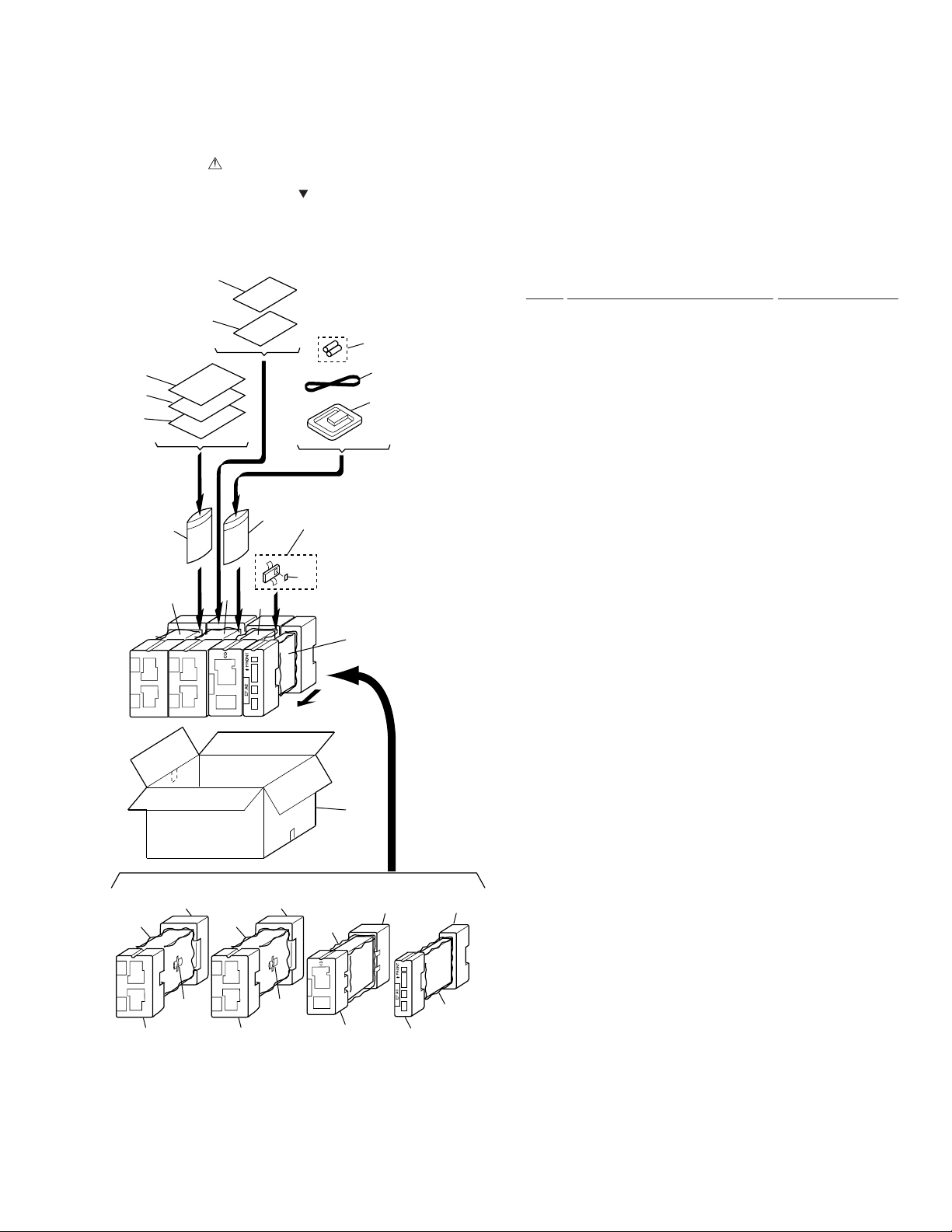
2.1 PACKING
The mark found on some component parts indicates the importance of the safety factor of the part.
•
Therefore, when replacing, be sure to use parts of identical designation.
Screws adjacent to mark on the product are used for disassembly.
•
PACKING PARTS LIST
9
•
Mark No. Description Part No.
XS-R9
11
10
5
14
8
16
16
4
4
13
19
3
FRONT
7
12
1
17
NSP 1 Remix Effector EF-R9(S)
2 • • • • •
NSP 3 Remix Control Mixer MX-R9(S)
NSP 4 Compact Disc Player PD-R9(S)
5 Caution Sheet ARM7034
6 • • • • •
7 FM Antenna ADH7010
8 Operating Instructions ARC7201
(German/Italian)
NSP 9 Warranty Card ARY7008
10 Operating Instructions ARC7202
(Spanish/Dutch)
11 Operating Instructions ARE7168
(English/French)
12 AM Loop Antenna ATB7009
13 Remote Control Unit AXD7148
(CU-SX123)
NSP 14 Dry Cell Battery (R6P,AA) VEM-013
15 • • • • •
16 Poly. Bag (0.03×230×340) Z21-038
17 Master Carton AHD7613
18 • • • • •
19 Battery Cover AZA7219
20 • • • • •
21 • • • • •
22 Mirror Mat (500×650×0.5) AHG7050
23 Pad F EF AHA7189
24 Pad R EF AHA7190
25 Mirror Mat DHL1050
26 Pad L AHA7191
27 Pad R AHA7192
28 Pad F CD AHA7187
29 Pad R CD AHA7188
NSP 30 Silicagel AEN7001
25
29
30 30
28
25
28
29
22
26
27
24
25
23
3
Page 4
XS-R9
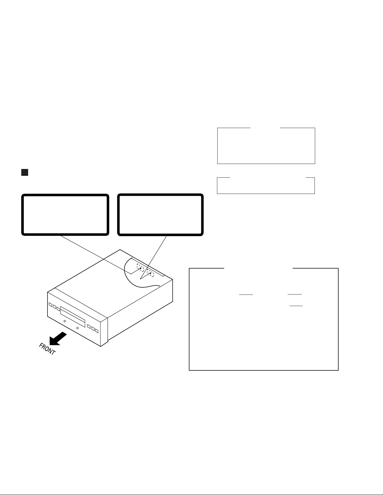
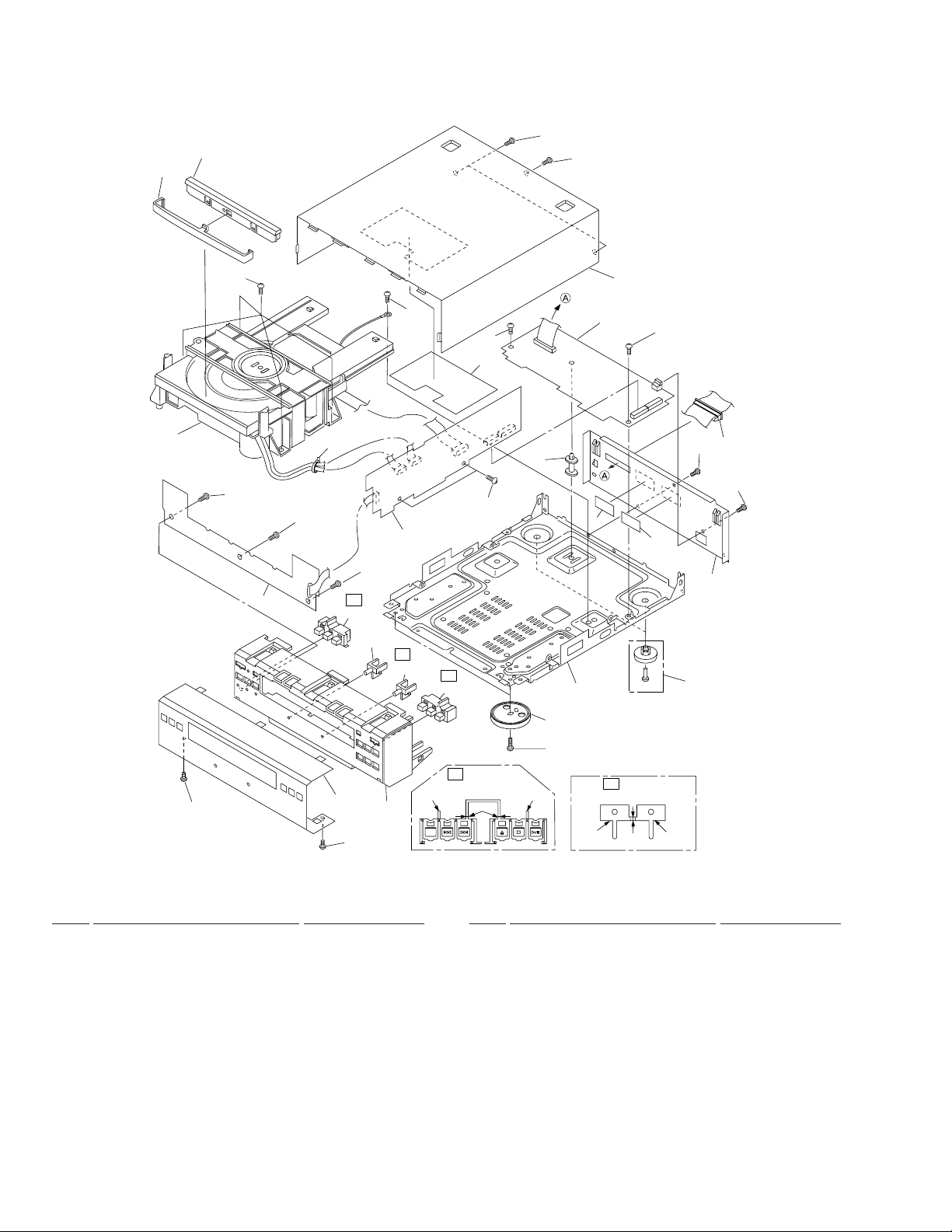
2.2 COMPACT DISC PLAYER [PD-R9(S)]
2.2.1 Exterior
11
12
22
22
20
9
Refer to
"2.3 SINGLE
MECHANISM ASSY".
21
17
25
19
24
23
7
21
1
21
2
∗1
10(1/2)
13(1/2)
∗2
13(2/2)
19
∗1
10(2/2)
15
3
27
5
19
4
22
22
26
6
8
18
COMPACT DISC PLAYER PARTS LIST
•
16
18
Mark No. Description Part No.
1 MAIN Assy AWU7142
2 FRONT Assy AWZ8889
3 REAR Assy AWU7144
4 Cord With Plug ADE7025
NSP 5 Chassis MD,CD,TC ANA7063
6 Rear Panel CD ANC7685
NSP 7 PCB Spacer AEC1371
8 Elastic Foot AEC7114
NSP 9 SINGLE MECHANISM Assy AXA7058
10 Play Button CD AAD7412
11 Tray Panel AAK7469
12 Tray Cap CD AAK7470
13 LED Lens CD,TCA AAK7472
14 Panel Base CDTC AMB7461
15 Insulator Assy AMR7189
4
22
Cut Position
∗1
10(1/2)
14
Cut
10(2/2)
13(1/2)
∗2
Cut Position
Cut
13(2/2)
Mark No. Description Part No.
16 AL Panel CD ANB7105
17 Bonnet MD,CD,TC AZN7701
18 Screw BBT30P080FZK
19 Screw BBZ30P060FCC
20 Screw BBZ30P100FMC
21 Screw PPZ30P080FMC
22 Screw VBZ30P080FZK
23 Binder (SKB-90BK) Z09-056
24 Rubber Sheet AEB7107
25 Screw PDZ30P050FMC
26 Caution Label HE PRW1233
27 Caution Label VRW1094
Page 5
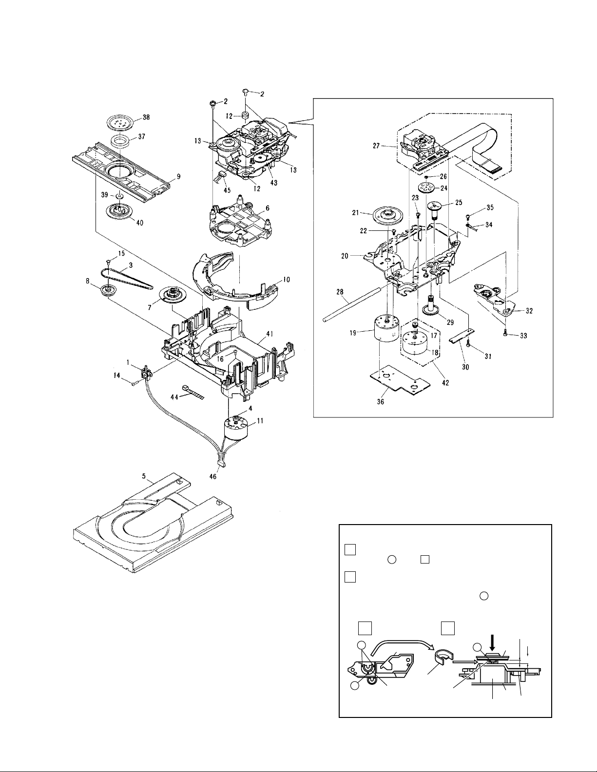
2.2.2 Single Mechanism Assy
1
• How to install the disc table
Use nipper or other tool to cut the three sections
marked figure . Then remove the spacer.
While supporting the spindle motor shaft with
the stopper, put spacer on top of the motor base
(angled so it doesn't touch section ), and stick
the disc table on top (takes about 9 kg pressure).
Take off the spacer.
1
2
1 2
A
A
A
B
6.9mm
3.1mm
± 0.05mm
FFC Holder
Spacer
Spacer
Spacer Setting
Position
Spindle Motor
Carriage
Base
Disc
Table
(Pressure of
about 9kg)
PCB
B
XS-R9
5
Page 6

XS-R9
SINGLE MECHANISM ASSY PARTS LIST
•
Mark No. Description Part No.
1 Lever Switch DSK1003
2 Screw PBA1048
3 Rubber Belt PEB1193
4 Motor Pulley PNW1634
5 Tray Black V PNW2455
6 Float Base PNW2032
7 Drive Gear 2 PNW2369
8 Gear Pulley PNW2034
9 Clamper Base PNW2375
10 Clamp Cam PNW2364
11 DC Motor/0.75W PXM1010
12 Float Rubber B REB1287
13 Float Rubber G REB1288
14 Screw BPZ26P060FMC
15 Screw Z39-019
16 Screw PMZ26P040FMC
17 Pinion Gear PNW2055
18 DC Motor (CARRIAGE) PXM1027
19 D.C. Motor Assy (SPINDLE) PEA1235
20 Carriage Base PNW2699
21 Disc Holder PNW1608
22 Screw JFZ20P030FNI
23 Screw JFZ17P025FZK
24 Gear 3 PNW2054
25 Gear 2 PNW2053
26 Washer WT12D032D025
27 Pickup Assy PEA1291
28 Guide Bar PLA1094
29 Gear 1 PNW2052
30 Gear Stopper PNB1303
31 Screw BPZ20P060FMC
32 FFC Holder PNW2057
33 Screw BPZ26P100FMC
34 Earth Lead Unit PDF1104
35 Screw BBZ26P060FMC
36 MECHANISM BOARD Assy PWX1192
37 Clamp Magnet PMF1014
NSP 39 H Rubber PEB1249
NSP 43 SERVO MECHANISM Assy AXA7017
38 Yoke PNB1216
40 Clamper S PNW1609
41 Loading Base AMR7190
42 D.C. Motor Assy (CARRIAGE)PEA1246
44 Binder Z09-056
45 Connector Assy (4P) RDE1043
46 Connector Assy (5P) PDE1239
6
Page 7
2.3 REMIX EFFECTOR [EF-R9(S)]
XS-R9
23
23
19
3
22
8
15
13
20
12
2
14
24
22
4
22
21
16
17
20
11
9
9
18
23
6
24
1
5
10
23
23
25
7
11
REMIX EFFECTOR PARTS LIST
•
Mark No. Description Part No. Mark No. Description Part No.
1 MAIN Assy AWU7067
2 FRONT Assy AWU7068
3 HEADPHONE Assy AWU7069
4 Lead Card 15P ADD7072
5 Cord With Plug ADE7016
NSP 6 Chassis SX,EF,RC ANA7062
7 Rear Panel EF ANC7687
8 Jack Plate ANG7158
9 MSPLS Support DEC1955
10 HEX. Screw KFS-4S-C1WM
11 Cushion REB1004
12 Jog Knob EF,RC AAB7182
13 Phone Knob EF AAB7139
14 Operation Button EF AAD7415
15 LED Lens EF AAK7477
NSP 18 Label VRW1629
16 Panel Base EF AMB7462
17 AL Panel EF ANB7107
19 Bonnet EF,RC AZN7702
20 Screw BBT30P080FZK
21 Screw PDZ30P050FMC
22 Screw PPZ30P080FMC
23 Screw VBZ30P080FZK
24 Screw ABA1021
25 Washer VEC1098
7
Page 8
XS-R9
2.4 REMIX CONTROL MIXER [MX-R9(S)]
23
∗1
Cut Position
13
12
30
15
11
8
5
18(1/2)
Cut
28
B
17
2
19
18(2/2)
20
18(2/2)
∗1
7
24
8
16(2/4)
∗2
14
16(1/4)
∗2
13
18(1/2)
∗1
21
7
24
A
A
3
16(4/4)
17
19
20
22
16(3/4)
∗2
∗2
∗2
Cut Position
16(1/4) 16(2/4) 16(3/4) 16(4/4)
B
Cut
Cut
29
10
9
27
26
29
29
29
32
4
9
10
6
8
Page 9

REMIX CONTROL MIXER PARTS LIST
•
Mark No. Description Part No.
XS-R9
NSP 2 VR Assy AWZ8899
NSP 26 Label VRW1629
1 MAIN Assy AWZ8898
3 Cord With Plug ADE7019
4 Bottom Plate ANF7009
5 Fader Stay ANG7159
6 PVC Sheet AEC7119
7 POM Ring AMR7188
8 Fader Sheet AWL7029
9 Screw BPZ30P300FMC
10 Disc Guard PNM1245
11 Equalizer Knob SX AAB7135
12 Tuning Knob SX AAB7136
13 Jog Knob CP AAB7140
14 Tempo Knob AAC7004
15 Fader Knob AAC7005
16 BPM Button AAD7417
17 Loop Button AAD7419
18 Sampler Button AAD7422
19 CUE Button AAD7423
20 LED Lens CP A AAK7476
21 Display Window CP AAK7478
22 FL filter CP AAK7479
23 Fader Cover AAK7480
24 LED Lens CP B AAK7507
25 Top Panel CP AMB7464
27 Screw BBZ30P060FCC
28 Screw BMZ20P030FMC
29 Screw PPZ30P080FMC
30 Screw CPZ30P080FZK
31 Fader Assy AZW7244
32 Rear Spacer AEC7126
9
Page 10
1
23
XS-R9
3. SCHEMATIC DIAGRAM
3.1 OVERALL CONNECTION DIAGRAM
A
4
DISPLAY ASSY
(AWU7132)
STEREO TUNER AMP
SX-R9/ZY
Refer to the service manual
RRV1937 for STEREO TUNER AMP
SX-R9/ZY.
B
FM/AM TUNER
MODULE
(AXQ7058)
SIDE ASSY
(AWU7133)
MAIN ASSY
(AWU7134)
TR ASSY
(AWU7141)
CONNECT ASSY
(AWU7137)
C
B
MAIN ASSY
(AWU7142)
MECHANISM BOARD ASSY
(PWX1192)
SINGLE MECHANISM ASSY
(AXA7058)
AA
COMPACT
C
DISC
PLAYER
PD-R9(S)
CD1
TEST PIN
for ADJ.
C C
REAR ASSY
(AWU7144)
FRONT ASSY
(AWZ8889)
1/2,
D
2/2
ADE7025
E
E E E
1/3,
MAIN ASSY
(AWU7067)
2/3,
3/3
FRONT ASSY
(AWU7068)
F
C
HEADPHONE ASSY
B
MAIN ASSY
(AWU7142)
MECHANISM BOARD ASSY
(PWX1192)
SINGLE MECHANISM ASSY
(AXA7058)
COMPACT
DISC
D
PLAYER
PD-R9(S)
CD2
TEST PIN
for ADJ.
C C
REAR ASSY
(AWU7144)
FRONT ASSY
(AWZ8889)
1/2,
D
2/2
ADE7025
MAIN ASSY
H
(AWZ8898)
REMIX
EFFECTOR
EF-R9(S)
(AWU7069)
G
VR ASSY
(AWZ8899)
I
REMIX CONTROL MIXER MX-R9(S)
10
1234
Page 11
5
678
XS-R9
Note : When ordering service parts, be sure to refer to "EXPLODED VIEWS and PAR TS LIST" or "PCB PARTS LIST".
HEADPHONE
ASSY
(AWU7138)
POWER ASSY
(AWU7135)
REG ASSY
(AWU7136)
SECONDARY
ASSY
(AWU7140)
POWER
TRANSFORMER
T1
ATS7215
PRIMARY
ASSY
(AWU7139)
AC
POWER
CORD
PDG1003
AC220V–230V
50/60Hz
A
B
CONNECT ASSY
(AWZ8894)
MAIN
ASSY
(AWZ8891)
DECK
MECHA
(RYM1264)
DECK
CT-R5/ZY
Refer to the service manual
RRV1933 for DECK CT-R5/ZY.
MCOM
ASSY
(AWZ8893)
FRONT ASSY
(AWZ8892)
MAIN ASSY
(AWU7152)
FRONT ASSY
MD MECHA ASSY
(AXA7054)
MINI DISC
RECORDER
MJ-R5/ZY
Refer to the service manual
RRV1934 for MINI DISC RECORDER MJ-R5/ZY.
C
(AWZ8887)
D
11
5
6
7
8
Page 12
1
23
XS-R9
3.2 COMPACT DISC PLAYER [PD-R9(S)]
3.2.1 OVERALL CONNECTIONS AND SINGLE MECHANISM ASSY
A
PICKUP ASSY
(PEA1291)
(TS)
(TS)
(FS)
(FS)
(TS)
(TS)
(FS)
(FS)
(TS)
(TS)
(FS)
(TS)
(TS)
(FS)
(TS)
(TS)
(FS)
4
(FS)
(FS)
(TS)
(TS)
(TS)
(FS)
(FS)
(TS)
(FS) (FS)
(TS)
(TS)
B
(FS)
(TS)
(FS)
(FS)
(TS)
(FS)
(FS)
(TS)
(FS)
(TS)
(FS)
(FS)
SINGLE MECHANISM ASSY
C
(AXA7058)
SIGNAL ROUTE
: RF SIGNAL ROUTE
(FS)
: FOCUS SERVO LOOP LINE
(TS)
: TRACKING SERVO LOOP LINE
(SM)
: SPINDLE MOTOR ROUTE
(CM)
: CARRIAGE MOTOR ROUTE
(LM)
: LOADING MOTOR ROUTE
MECHANISM BOARD ASSY
A
(PWX1192)
S601
CLAMP SW
(DSK1003)
(SM)
(CM)
(LM)
D
12
A
LOADING
MOTOR
(PXM1010)
1234
Page 13
TEST PIN
for ADJ.
5
678
XS-R9
A
D
FRONT ASSY
(AWZ8889)
B
MAIN ASSY
B
(AWU7142)
C
1/2,
C C
REAR ASSY
(AWU7144)
2/2
CN103:CD1,CN104:CD2
1/3
E
C
MINI DISC
RECORDER
(MJ-R5/ZY)
MAIN ASSY
JA501
CONNECTOR
ASSY
PDE1239
D
13
5
6
7
8
Page 14
1
23
XS-R9
3.2.2 MAIN, REAR(1/2) AND FRONT ASSEMBLIES
MAIN ASSY
B
(FS)
A
(TS)
(FS)
(TS)
(LM)
B
TO SINGLE MECHANISM ASSY
(AWU7142)
C415
GNDD
33p
470
F401
(D)
ATF7013
1SS355
(D)
470
(A)
1SS355
470
4
470
+5.0V
1SS355
(SM)
(CM)
(LM)
(SM)
(LM)
(LM)
UDZS6.2B
(LM)
(SM)
(SM)
VNF1084
(A)
(D)
C
TEST PIN for ADJ.
(FS)
(CM)
(FS)
(TS)
(TS)
(TS)
(CM)
(FS)
(TS)
(TS)
D
14
B
(FS)
(TS)
1234
Page 15
5
678
XS-R9
A
S701 : PLAY/PAUSE
S702 : STOP
S703 : OPEN/CLOSE
S704 : SEARCH
S705 : SEARCH
S706 : REPEAT
(LM)
(LM)
(LM)
(LM)
2SC2412K
C
D701,D702 : SLR-342VCT31
REAR ASSY
(AWU7144)
1/2
1SS355
MICROCOMPUTER
2SC2412K
(LM)
(LM)
FRONT ASSY
D
(AWZ8889)
(D)
(A)
B
2/2
C
C
SIGNAL ROUTE
: RF SIGNAL ROUTE
(D)
: DIGITAL AUDIO OUTPUT
(A)
: ANALOG AUDIO OUTPUT
(FS)
: FOCUS SERVO LOOP LINE
5
(TS)
: TRACKING SERVO LOOP LINE
(SM)
: SPINDLE MOTOR ROUTE
(CM)
: CARRIAGE MOTOR ROUTE
(LM)
: LOADING MOTOR ROUTE
6
D
B
7
C
1/2
D
8
15
Page 16
1
XS-R9
3.2.3 REAR ASSY(2/2)
A
B
R327
R345
L313-L315:
PTL1014
0
330
HM514800CJ-7
R349
0
L314
47
R346
470
R348 330L313
0
R319
R320 R347
23
MJ-R5/ZY
MAIN ASSY
JA501
(D)
C317
0.01
C
REAR ASSY
(AWU7144)
2/2
L151
10
4
C318
33p
C319
33p
C
68
R318
56p
C327
MN19413A
DSP IC
BUILT-IN
DAC
R382 2.7k
R384
R381
2.7k
R383 2.7k
L304
(A)
2.7k
(A)
68
D
16
2/2
C
1234
Page 17
(D)
5
678
XS-R9
SIGNAL ROUTE
(D)
: DIGITAL AUDIO OUTPUT
(A)
(A)
+5.0V
+5.0V
C
1/2
Q103
2SD2395
: ANALOG AUDIO OUTPUT
+5.0V
A
B
1.2k
1.2k
1.2k
1.2k
CAUTION : FOR CONTINUED PROTECTION AGAINST
RISK OF FIRE. REPLACE ONLY WITH
SAME TYPE NO. AEK7006 MFD, BY
LITTELFUSE INK. FOR IC101.
IC351(2/2)
NJM2068M
IC351(1/2)
NJM2068M
(A)
1SS355
1SS355
IC352(2/2)
NJM2068M
IC352(1/2)
NJM2068M
-5.0V
+7.3V
-7.3V
CN103:(CD1),CN104:(CD2)
1/3
(A)
VNF1084
(A)
E
C
D
2/2
C
5
6
7
8
17
Page 18
1
XS-R9
3.3 REMIX EFFECTOR [EF-R9(S)]
3.3.1 OVERALL CONNECTION DIAGRAM
A
CN102
H
23
2/2
C
CN101(CD1)
4
E
B
C
E E E
1/3,
MAIN ASSY
(AWU7067)
2/3,
3/3
FRONT ASSY
(AWU7068)
D
HEADPHONE ASSY
(AWU7069)
G
18
1234
F
Page 19
5
678
XS-R9
A
2/2
C
CN101(CD2)
B
MAIN ASSY CN104
STEREO TUNER AMP(SX-R9/ZY)
C
D
19
5
6
7
8
Page 20
1
XS-R9
3.3.2 MAIN ASSY(1/3)
H
A
CN102
23
NC
2/3
E
IC310(1/2)
BA4558F
IC310(2/2)
BA4558F
4
CD2 VCA CONTROL
1/3
E
(CD1)
B
E
2/3
IC408(2/2)
BA4558F
IC408(1/2)
BA4558F
1/3
E
IC409(2/2)
BA4558F
IC409(1/2)
BA4558F
IC410(2/2)
BA4558F
CD1 VCA CONTROL
11
A
11
B
CN101(CD1)
2/2
C
(CD2)
(CD1)
BA4558F
IC406(2/2)
BA4558FIC405(2/2)
IC407(2/2)
BA4558F
IC410(1/2)
BA4558F
12
(CD1)
A
12
B
C
IC405(1/2)
BA4558F
IC406(1/2)
BA4558F
IC403(2/2)
BA4558F
IC407(1/2)
BA4558F
IC404(2/2)
BA4558F
13
E
2/3
14
A
A
(CD2)
CN101(CD2)
2/2
C
D
2/3
E
(CD1)
(CD2)
20
1/3
E
1234
IC401(2/2)
BA4558F
IC401(1/2)
BA4558F
IC402(2/2)
BA4558F
IC402(1/2)
BA4558F
IC403(1/2)
BA4558F
IC404(1/2)
BA4558F
13
(CD2)
2/3
E
B
14
B
(CD1)
Page 21
5
678
XS-R9
(CD1)
E
E
2/3
2/3
CAUTION : FOR CONTINUED PROTECTION AGAINST
RISK OF FIRE. REPLACE ONLY WITH
SAME TYPE NO. AEK7003 MFD, BY
LITTELFUSE INK. FOR IC101.
E
MAIN ASSY
1/3
(AWU7067)
5.009V
(CD1)
VCA IC
315mA
CAUTION : FOR CONTINUED PROTECTION AGAINST
RISK OF FIRE. REPLACE ONLY WITH
SAME TYPE NO. AEK7020 MFD, BY
LITTELFUSE INK. FOR IC102.
-4.98V
125mA
-7.06V
-6.20V
E
E
2/3
1/3
A
B
SX-R9/ZY MAIN ASSY CN104
(CD2)
E
E
E
2/3
2/3
3/3
VCA IC
IC306(1/2)
BA4558F
IC307
(1/2)
BA4558F
IC309(1/2)
NJM2068M
IC305(1/2)
BA4558F
IC305(2/2)
BA4558F
IC309(2/2)
NJM2068M
E
E
3/3
E
3/3
2/3
E
C
2/3
E
3/3
IC306(2/2)
BA4558F
5
IC307(2/2)
BA4558F
D
2/3
E
SIGNAL ROUTE
(CD1)
: CD1 AUDIO SIGNAL
(CD2)
: CD2 AUDIO SIGNAL
: AUDIO SIGNAL
1/3
E
6
7
8
21
Page 22
1
23
XS-R9
3.3.3 MAIN(2/3), FRONT AND HEADPHONE ASSEMBLIES
F801
ATF7016
A
C847
0.01
C848
0.01
IC801(1/2)
IC801(2/2)
C841
C842
47p
C843
R841
R842
C844
47p
4
220p
10
10
220p
B
IC802(1/2)
IC802(2/2)
HEADPHONE ASSY
(AWU7069)
G
C
S701 : EFFECT ON/OFF
S702 : DELAY
S703 : ECHO
S704 : PAN
S709 : FRANGER
S710 : KEYCON
S711 : OLD
S712 : SAMPLE
S751 : EFFECT LEVEL
FRONT ASSY
F
(AWU7068)
D
22
2/3
E
1234
F
G
Page 23
5
678
XS-R9
SIGNAL ROUTE
: AUDIO SIGNAL
(CD1)
: CD1 AUDIO SIGNAL
E
A
1/3
B
E
2/3
1/3
E
1/3
E
MAIN ASSY
(AWU7067)
H.P. CD1&CD2/CD1/CD2 SELECT
(CD1)
3/3
E
4
E
1/3
MICROCOMPUTER
1
2
3
6
5
X1
X2
1/3
E
C
3/3
E
1/3
E
3/3
E
1/3
E
D
2/3
E
5
6
7
8
23
Page 24
1
XS-R9
3.3.4 MAIN ASSY(3/3)
E
A
3/3
MAIN ASSY(AWU7067)
23
4
47
R275
0
R281
0
R261
B
R276
47×4
DCN1090
7
HM514400CJ-7
R280 0 R274 47
R279 0 R273 47
R278 0 R272 47
R277 0 R271 47
C233
0.01
10
9
MN19413A
2/3
8
DSP IC
E
C
E
1/3
D
24
3/3
E
1234
Page 25

5
V5D2 V+7 V+7VAD5
Q103
2SD1859X
V+5V
C113
GNDP GNDP GNDP GNDA GNDA
J102
DB017ND0
0.01
DTA124EK
47
R104
D102
UDZS5.6B
Q105
56
R105
C102
100/10
GNDP
L101
22
C112
0.01
678
L203
22
Q102
2SD1859X
R103
DTA124EK
47
D107
UDZS5.6B
Q109
R109
C109
220
100/10
J101
ADB-005
0.01
C114
GNDP
Q106
DTC124EK
GNDD
E
PWR
(2/3)
2/3
XS-R9
A
B
GNDP
GNDD
IC204(2/2)
BA4558F
DSP L.P.F OUTPUT
IC204(1/2)
BA4558F
IC205(1/2)
BA4558F
IC205(2/2)
BA4558F
E
1/3
E
1/3
E
C
2/3
D
3/3
E
5
6
7
8
25
Page 26

XS-R9
WAVEFORMS OF REMIX EFFECTOR [EF-R9(S)]
•
Note :
No.
in the table correspond to the measurement points of schematic diagrams.
MAIN ASSY (1/3)
1/3
E
11
A
BP1L (CD1 PLAY MODE)
11
B
BP2L (CD2 PLAY MODE)
12
A
BP1M (CD1 PLAY MODE)
12
B
BP2M (CD2 PLAY MODE)
14
A
BP1H (CD1 PLAY MODE)
14
B
BP2H (CD2 PLAY MODE)
• CD1 PAD TRIM VOL – 6dB
(Output level of receiver Rec
Out 0.42VRMS)
2V/div, 10ms/div, f=24Hz
11
A (11B)
12
A (12B)
14
A (14B)
MAIN ASSY (2/3)
2/3
E
4
IC601-Pin 61 (CS)
IC601-Pin 11 (DISP SI)
1
IC601-Pin 12 (DISP SO)
2
IC601-Pin 13 (DISP CLK)
3
PLAY MODE
5V/div, 5ms/div
11
A
BP1L (CD1 PLAY MODE)
11
B
BP2L (CD2 PLAY MODE)
12
A
BP1M (CD1 PLAY MODE)
12
B
BP2M (CD2 PLAY MODE)
13
A
BP1H (CD1 PLAY MODE)
13
B
BP2H (CD2 PLAY MODE)
14
A
BP1H (CD1 PLAY MODE)
14
B
BP2H (CD2 PLAY MODE)
• CD1 PAD TRIM VOL – 6dB
(Output level of receiver Rec
Out 0.43VRMS)
2V/div, 20µs/div, f=8Hz
11
A (11B)
12
A (12B)
13
A (13B)
14
A (14B)
6
X1 IC601-Pin 70 (X1)
X2 IC601-Pin 69 (X2)
5
PLAY MODE
2V/div, 200ns/div
11
A
BP1L (CD1 PLAY MODE)
11
B
BP2L (CD2 PLAY MODE)
12
A
BP1M (CD1 PLAY MODE)
12
B
BP2M (CD2 PLAY MODE)
14
A
BP1H (CD1 PLAY MODE)
14
B
BP2H (CD2 PLAY MODE)
• CD1 PAD TRIM VOL – 6dB
(Output level of receiver Rec
Out 0.43VRMS)
2V/div, 500µs/div, f=500Hz
11
A (11B)
12
A (12B)
14
A (14B)
26
E
3/3
7
8
4
1
2
3
MAIN ASSY (3/3)
IC201-Pin 65 (XI1)
IC201-Pin 66 (XO1)
7
8
PLAY MODE
5V/div, 50ns/div
6
5
9
IC201-Pin 24 (SDA)
IC201-Pin 23 (SCL)
10
9
10
PLAY MODE
2V/div, 20µs/div
Page 27

1
234
3.4 REMIX CONTROL MIXER [MX-R9(S)]
3.4.1 OVERALL CONNECTION DIAGRAM
CN102
E
1/3
XS-R9
A
B
MAIN ASSY
H
(AWZ8898)
C
VR ASSY
I
(AWZ8899)
27
1
2
3
4
D
Page 28

1
23
XS-R9
3.4.2 MAIN AND VR ASSEMBLIES
4
A
B
MAIN ASSY
H
(AWZ8898)
5.0V
TEST
MICROCOMPUTER
ASG1034
1SS355
C
S104–S129:
ASG1034
1SS355
1SS355
D
VR ASSY
I
(AWZ8899)
–17V
+5.0V
IC102(1/2)
BA4558F
IC102(2/2)
BA4558F
1SS355
1SS355
1SS355
1SS355
28
H
I
1234
Page 29

5
678
XS-R9
A
FL Spacer
AEB7095 × 2
AAV7046
V101
–34V
3.1V
FADER
Center
10.5Vp-p
8.4Vp-p
–23V
–23V
+5.0V
+5.0V
3.1V
FADER
Center
+5.0V
CN102
1/3
E
B
C
S101 : EFFECT JOG
S102 : JOG1
S103 : JOG2
S104 : SAMPLER PLAY
S105 : CD1 MASTER TEMPO
S106 : REMIX
S107 : CD2 TIME/AUTO CUE
S108 : CD1
S109 : CD1 TIME/AUTO CUE
S110 : CD2 LOOP
S111 : CD2
S112 : CD1 CUE
S113 : CD1
S114 : CD2 MASTER TEMPO
S115 : CD2 CUE
S116 : CD1
S117 : CD1
S118 : MONITER SELECT
S119 : CD2
S120 : SAMPLER MEMORY
S121 : CD1 LOOP
S122 : FADER START
S123 : CD2
S124 : A.B.E.
S125 : EFFECT ON/OFF
S126 : BPM/TIME
S127 : CD2
S128 : EFFECT SELECT
S129 : EFFECT MODE
S130 : TAP
H
5
6
7
8
29
D
Page 30

1
23
XS-R9
4. PCB CONNECTION DIAGRAM
A
NOTE FOR PCB DIAGRAMS :
1. Part numbers in PCB diagrams match those in the schematic
diagrams.
2. A comparison between the main parts of PCB and schematic
diagrams is shown below.
Symbol In PCB
Diagrams
BCE
BCE
D
Symbol In Schematic
Diagrams
BCEBCE
BCE
DGGSS
BCE
DGS
Part Name
Transistor
Transistor
with resistor
Field effect
transistor
4
3. The parts mounted on this PCB include all necessary parts for
several destinations.
For further information for respective destinations, be sure to
check with the schematic diagram.
4. View point of PCB diagrams.
Connector
Capacitor
SIDE A
P.C.Board
Chip Part
SIDE B
B
Resistor array
3-terminal
regulator
4.1 COMPACT DISC PLAYER [PD-R9(S)]
4.1.1 MECHANISM BOARD ASSY
MECHANISM BOARD ASSY
A
C
SPINDLE
MOTOR
INSIDE
M
CARRIAGE
MOTOR
M
(PNP1239-C)
CN405
B
SIDE A
D
30
A
1234
Page 31

1
CN102
C
MAIN
ASSY
B
MAIN
ASSY
B
CN103
C
(ANP7204-D)
(ANP7204-D)
J701
D
TO PICKUP
ASSY
CN102
SINGLE
MECHANISM
ASSY
CN610
A
IC451
IC452
IC401
IC501
IC601
IC602
VR601
VR602
Q401
VC451
4.1.2 MAIN ASSY
234
XS-R9
A
B
C
D
SIDE A SIDE B
1
2
3
B
4
31
Page 32

1
XS-R9
4.1.3 REAR ASSY
23
4
A
REAR ASSY
C
B
CN402
B
CN401
Q151
MJ-R5/ZY
MAIN ASSY
IC301
IC303
B
IC302
IC351
Q353 Q354
IC352
Q351
Q352
C
Q202
Q201 Q203
IC102 IC101
Q101
IC201
E
CN103 : CD1
CN104 : CD2
Q104
Q106
Q107
Q102
Q103
D
(ANP7204-D)
32
SIDE A
C
1234
Page 33

1
234
XS-R9
A
REAR ASSY
C
B
C
(ANP7204-D)
D
SIDE B
C
1
2
3
4
33
Page 34

1
XS-R9
4.1.4 FRONT ASSY
A
B
FRONT ASSY
D
23
FRONT ASSY
D
4
C
D
CN408
B
(ANP7204-D)
(ANP7204-D)
SIDE A SIDE B
34
D
1234
Page 35

1
234
4.2 REMIX EFFECTOR [EF-R9(S)]
XS-R9
4.2.1 FRONT AND HEADPHONE ASSEMBLIES
FRONT ASSY
F
HEADPHONE ASSY
G
E
CN603
CN601
E
A
(ANP7251-A)
B
SIDE A
FRONT ASSY
F
G
1
HEADPHONE ASSY
2
C
(ANP7251-A)
D
SIDE B
GF
3
4
35
Page 36

XS-R9
4.2.2 MAIN ASSY
J601
G
A
B
1
MAIN ASSY
E
23
4
C
CN101
(CD1)
H
CN102
C
CN101
(CD2)
C
SX-R9/ZY
MAIN
ASSY
F
CN602
CN104
(ANP7251-A)
D
Q651-Q658 IC601
Q102Q531 Q109 IC201
IC401-IC404
Q106
Q108
IC204
Q603
IC502 IC501
Q101 Q104IC101 IC102
IC202
IC205
Q301-Q304 IC310IC301-IC304
IC306-IC309
Q103Q201 Q202
Q105IC405-IC410
SIDE A
36
E
1234
Page 37

1
(
)
234
XS-R9
MAIN ASSY
E
A
B
C
ANP7251-A
D
SIDE B
E
1
2
3
4
37
Page 38

1
23
XS-R9
4.3 REMIX CONTROL MIXER [MX-R9(S)]
4.3.1 MAIN AND VR ASSEMBLIES
A
MAIN ASSY
H
E
CN102
B
4
C
D
VR ASSY
I
SIDE A
38
H I
1234
Page 39

5
678
XS-R9
A
IC101
Q101
B
VR102 VR103
VR104 VR105
IC102
Q106
C
Q102-Q105
D
(ANP7207-C)
SIDE A
H I
5
6
7
8
39
Page 40

A
Y
B
XS-R9
1
MAIN ASSY
H
23
4
C
D
VR ASS
I
SIDE B
40
H I
1234
Page 41

5
678
XS-R9
A
B
R ASSY
C
D
(ANP7207-C)
SIDE B
H I
5
6
7
8
41
Page 42

XS-R9
Mark No. Description Part No.
Mark No. Description Part No.
5. PCB PARTS LIST
NOTES:•Parts marked by "NSP" are generally unavailable because they are not in our Master Spare Parts List.
The mark found on some component parts indicates the importance of the safety factor of the part.
•
Therefore, when replacing, be sure to use parts of identical designation.
When ordering resistors, first convert resistance values into code form as shown in the following examples.
•
Ex.1 When there are 2 effective digits (any digit apart from 0), such as 560 ohm and 47k ohm (tolerance is shown by J=5%,
and K=10%).
560 Ω→56 × 10
47k Ω→47 × 103→ 473 ........................................................ RD1/4PU 4 7 3 J
0.5 Ω→R50 ..................................................................................... RN2H
1 Ω→1R0 ..................................................................................... RS1P
Ex.2 When there are 3 effective digits (such as in high precision metal film resistors).
5.62k Ω→ 562 × 10
Mark No. Description Part No.
LIST OF ASSEMBLIES
NSP COMPACT DISC PLAYER PD-R9(S)
NSP SINGLE MECHANISM ASSY AXA7058
NSP SERVO MECHANISM ASSY AXA7017
NSP CD MAIN ASSY AWM7372
NSP REMIX EFFECTOR EF-R9(S)
NSP EF MAIN ASSY AWM7366
NSP REMIX CONTROL MIXER MX-R9(S)
NSP PAD MAIN ASSY AWM7304
NSP VR ASSY AWZ8899
MECHANISM BOARD ASSY PWX1192
MAIN ASSY AWU7142
REAR ASSY AWU7144
FRONT ASSY AWZ8889
MAIN ASSY AWU7067
FRONT ASSY AWU7068
HEADPHONE ASSY AWU7069
MAIN ASSY AWZ8898
COMPACT DISC PLAYER [PD-R9(S)]
MECHANISM BOARD ASSY
A
SWITCH
S610 DSG1016
1
→ 561 ........................................................ RD1/4PU 5 6 1 J
R 5 0
1 R 0
1
→ 5621 ...................................................... RN1/4PC 5 6 2 1 F
Mark No. Description Part No.
IC452 TC7SU04F
Q401 2SK246
D401-D403 1SS355
D601 UDZS6.2B
COIL AND FILTER
F401 CHIP EMI FILTER ATF7013
L401 LCTA220J3225
CAPACITORS
VC451 (45pF) ACM7002
C412,C413 CCSQCH101J50
C454,C511 CCSQCH102J50
C405,C406 CCSQCH150J50
C415 CCSQCH330J50
C604 CCSQCH561J50
C517 CEAL101M6R3
C455 CEAT101M10
C601,C602 CEAT331M10
C452 CEAT3R3M50
C451 CEAT470M16
C408 CEAT471M6R3
C504,C516 CEAT4R7M50
C403 CEATR47M50
C407 CEJA470M10
C453 CFTYA474J50
C404,C409-C411,C456,C457 CKSQYB103K50
C506,C507,C509,C514,C515 CKSQYB103K50
C518,C519,C603,C605,C606 CKSQYB103K50
C608-C610 CKSQYB103K50
K
K
OTHERS
CN610 MT CONNECTOR 4P 173979-4
MAIN ASSY
B
SEMICONDUCTORS
IC451 BA7042
IC501 CXA1372BQ
IC401 CXD2500BQ
IC602 LA6517
IC601 LA6520
42
C607 CKSQYB104K25
C401 CKSQYB152K50
C508,C510,C513 CKSQYB333K50
C512 CKSQYB472K50
C402 CKSQYB473K50
C501-C503,C505 CKSQYF104Z50
RESISTORS
VR601,VR602 (22kΩ) RCP1103
Other Resistors RS1/10S J
Page 43

XS-R9
Mark No. Description Part No.
OTHERS
CN403 CONNECTOR 12P 12FMZ-ABT
CN405 MT CONNECTOR 4P 173981-4
CN404 MT CONNECTOR 5P 173981-5
CN408 4P JUMPER CONNECTOR 52151-0410
X401 CRYSTAL RESONATOR PSS1008
CN401 CONNECTOR 14P TUC-P14X-B1
CN402 CONNECTOR 15P TUC-P15X-B1
CN406 6P SIDE POST VKN-004
KN601 EARTH METAL FITTING VNF1084
REAR ASSY
C
(16.9344MHz)
PCB BINDER VEF1040
SEMICONDUCTORS
IC101 (630mA) AEK7006
IC302 HM514800CJ-7
IC301 MN19413A
IC351,IC352 NJM2068M
IC201 PD4866A
Q201 2SC2412K
Q101,Q104 2SC4040
Q351,Q352 2SD2114K
Q103 2SD2395
Q106,Q203,Q354 DTA143EK
Q202 DTC124EK
Q107,Q151,Q353 DTC143EK
D201,D301,D302 1SS355
D102 UDZS5.1B
D101,D103,D104 UDZS5.6B
Mark No. Description Part No.
RESISTORS
All Resistors RS1/10S J
OTHERS
CN101 CONNECTOR 19P AKP7002
JA151 OPTICAL LINK OUT GP1F32T
CN103 CONNECTOR 14P TUC-P14P-B1
CN102 CONNECTOR 15P TUC-P15P-B1
KN101 EARTH METAL FITTING VNF1084
X201 CERAMIC RESONATOR VSS1014
FRONT ASSY
D
PCB BINDER VEF1040
(4.19MHz)
SEMICONDUCTORS
Q701 2SC2412K
D701,D702 SLR-342VCT31
SWITCHES
S701-S706 ASG1034
RESISTORS
All Resistors RS1/10S J
OTHERS
701 4P CABLE HOLDER 51048-0400
J701 JUMPER WIRE 4P D20PDY0415E
COILS
L151 LCTA100J3225
L304 LCTA680J3225
L201,L301,L302 LFA220J
L313,L314 CHIP BEADS PTL1014
CAPACITORS
C210,C313,C314,C353-C356 CCSQCH101J50
C359,C360 CCSQCH101J50
C351,C352 CCSQCH102J50
C318,C319,C369,C370 CCSQCH330J50
C203-C205 CCSQCH391J50
C327 CCSQCH560J50
C361,C362 CCSQSL182J50
C102-C104,C301 CEAT101M10
C304 CEAT1R0M50
C363,C364,C371,C372 CEAT220M50
C101,C315,C365-C368 CEAT470M16
C201 CEAT471M6R3
C305,C307 CEZA220M25
C357,C358 CEZA2R2M50
C151,C212-C214,C302,C303 CKSQYB103K50
C309-C312,C316,C317,C321 CKSQYB103K50
C324,C325 CKSQYB103K50
C153,C202,C215,C306,C308 CKSQYB104K25
C323 CKSQYB104K25
C206,C207,C209,C211 CKSQYB471K50
C152,C154 CKSQYF104Z50
C208 CKSQYF105Z16
REMIX EFFECTOR [EF-R9(S)]
MAIN ASSY
E
SEMICONDUCTORS
IC101 (315mA) AEK7003
IC102 (125mA) AEK7020
IC204,IC205,IC305-IC307,IC310 BA4558F-HT
IC401-IC410,IC502 BA4558F-HT
IC308,IC501 BU4052BCF
IC303,IC304 BU4066BCF
IC202 HM514400CJ-7
IC301,IC302 M51131L
IC201 MN19413A
IC309 NJM2068M
IC601 PD4867A
Q108,Q531,Q603,Q651-Q658 2SA1037K
Q104 2SB1238X
Q101-Q103 2SD1859X
Q201,Q202 2SD2114K
Q105,Q109,Q301-Q304 DTA124EK
Q203 DTA143EK
Q106 DTC124EK
Q601 DTC143EK
D104-D106,D605 1SR154-400
D401,D402,D404-D406 1SS355
D408-D410,D412,D413 1SS355
D415,D416,D418,D419 1SS355
D601-D604,D606-D608 1SS355
D611-D618 1SS355
D411,D414,D417,D420 UDZS5.1B
D101-D103,D107,D403,D407 UDZS5.6B
43
Page 44

XS-R9
Mark No. Description Part No.
COILS
L601 LCTA220J3225
L101,L201-L203 LFA220J
CAPACITORS
C222,C223,C271,C272 CCSQCH101J50
C321,C322,C341-C344 CCSQCH101J50
C401,C402,C525,C526 CCSQCH101J50
C609,C610,C614,C616 CCSQCH101J50
C224,C225,C263,C264 CCSQCH330J50
C253-C256,C259,C260 CCSQCH471J50
C251,C252 CCSQSL152J50
C345,C346 CEAL100M35
C257,C258,C267-C270 CEAL2R2M50
C311-C314,C323,C324 CEAL2R2M50
C349-C352,C383-C390 CEAL2R2M50
C511-C514,C523,C524 CEAL2R2M50
C527,C528,C604 CEAL2R2M50
C101-C103,C109 CEAT101M10
C301-C304 CEAT2R2M50
C207,C208,C211,C213,C215 CEAT470M16
C217,C219,C228,C232 CEAT470M16
C305,C306 CEAT470M16
C601 CEJA101M10
C265,C266,C315,C316 CEJA470M16
C353,C354 CEJA470M16
C605,C618 CEJA470M35
C273,C274 CKSQYB102K50
C112-C114,C201-C205 CKSQYB103K50
C209,C210,C212,C214,C216 CKSQYB103K50
C218,C220,C221,C229,C233 CKSQYB103K50
C307,C308,C325-C328 CKSQYB103K50
C361,C362,C381,C382 CKSQYB103K50
C391,C392,C403-C416 CKSQYB103K50
C421-C426,C431-C436 CKSQYB103K50
C501,C502,C602,C603 CKSQYB103K50
C606-C608,C611-C613,C615 CKSQYB103K50
C419,C420,C427-C430 CKSQYB104K25
C443,C444 CKSQYB104K25
C417,C418 CKSQYB183K50
C261,C262 CKSQYB332K50
C104-C107,C275 CKSQYF104Z50
C108,C439-C442,C617 CKSQYF105Z16
Mark No. Description Part No.
FRONT ASSY
F
SEMICONDUCTORS
D651 SLR-342MCT31
D652-D658 SLR-342VCT31
SWITCHES
S701-S704,S709-S712 ASG1034
S751 ASX7015
RESISTORS
All Resistors RS1/10S J
OTHERS
CN602 15P FFC CONNECTOR 9604S-15F
HEADPHONE ASSY
G
SEMICONDUCTORS
IC801,IC802 BA4560F
Q801,Q803,Q804 2SD2114K
COIL AND FILTER
F801 EMI FILTER ATF7016
L801 LCTA2R2J3225
CAPACITORS
C823,C824 CCSQCH101J50
C825,C826 CCSQCH151J50
C843-C846 CCSQCH221J50
C841,C842 CCSQCH470J50
C835,C836 CEAL2R2M50
C821,C822 CEJA100M16
C827,C828,C833,C834 CEJA101M6R3
C831,C832 CKSQYB103K50
C847,C848 CKSQYB223K50
C840 CKSQYF104Z50
RESISTORS
R803,R804 (1Ω) ACN1104
VR821 (10kΩ-B) ACS7025
Other Resistors RS1/10S J
RESISTORS
R276 (47Ω) DCN1090
Other Resistors RS1/10S J
OTHERS
CN603 6P JUMPER CONNECTOR 52147-0610
CN101 20P JUMPER CONNECTOR 52328-2020
CN601 15P FFC CONNECTOR 9604S-15C
CN102 D-SUB MINI 15P AKP7019
X201 CRYSTAL RESONATOR PSS1008
KN101 EARTH METAL FITTING VNF1084
X601 CERAMIC RESONATOR VSS1014
(4.19MHz)
44
OTHERS
J601 JUMPER WIRE 6P D20PWY0610E
JA821 STEREO JACK KN-083
19P SOCKET AKP7001
(16.9344MHz)
Page 45

XS-R9
Mark No. Description Part No.
REMIX CONTROL MIXER [MX-R9(S)]
MAIN ASSY
H
SEMICONDUCTORS
IC102 BA4558F-HT
IC101 PDG208A
Q101-Q106 DTC143ES
D101-D103,D105-D108 1SS355
D110-D114 SLR-342MCT31
D116 SLR-342VCT31
D104 UDZ16B
COILS
L101,L102 LCTA220J3225
SWITCHES
S104-S130 ASG1034
S102,S103 ASX7016
S101 ASX7019
CAPACITORS
C105,C109-C111 CCSQCH101J50
C129 CEAT100M50
C123,C127 CEAT470M16
C201 CEAT470M50
C101,C104 CEAT471M6R3
Mark No. Description Part No.
C102,C103,C106-C108 CKSQYB103K50
C112-C119,C124-C126,C128 CKSQYB103K50
C132,C144,C145 CKSQYB103K50
C122,C135,C146 CKSQYF104Z50
C120 CKSQYF105Z16
C121,C140-C143 CKSQYF473Z50
RESISTORS
R159 RA12T104J
R156,R158 RA15T104J
R157 RA5T104J
VR104,VR105 (10kΩ-B) ACS7026
VR102,VR103 (10kΩ-B) ACU7001
Other Resistors RS1/10S J
OTHERS
X101 CERAMIC RESONATOR EFOEC8004A4
V101 FL TUBE AAV7046
J101 CONNECTOR ASSY PG03MR-E10
VR ASSY
I
RESISTORS
VR101 (10kΩ-B) ACU7002
Other Resistors RS1/10S J
PORON SHEET AEB7095
OTHERS
CN101 MT CONNECTOR 3P 173979-3
45
Page 46

XS-R9
6. ADJUSTMENT
6.1 ADJUSTMENT OF COMPACT DISC PLAYER [PD-R9(S)]
6.1.1 PREPARATIONS
1. Jigs and Measuring Instruments
8-cm DISC
(With at least about
20 minutes recording)
Ball point hexagon wrench
(size: 1.5mm)
GGK1002
2. Necessary Adjustment Points
When Adjustment points
Exchange
CD TEST DISC
(YEDS-7)
screwdriver
(large)
PICKUP
Precise
screwdriver
Low-frequency
oscillator
screwdriver
(small)
Dual-trace
oscilloscope
(10 : 1 probe)
2. 3. 4. 5. 6. 7. → Page 48 to 51
screwdriver
(medium)
39 kΩ
0.001µF
Low pass filter
(39 kΩ + 0.001µF)
Exchange
MAIN ASSY
Exchange
SERVO MECH ASSY
Exchange
SPINDLE MOTOR
46
1. 2. 3. 5. 6. 7. → Page 48 to 51
2. 3. 4. 5. 6. 7. → Page 48 to 51
ADJ → Page 5
Page 47

6.1.2 ADJUSTMENT
1. How to Start/Cancel Test Mode
TEST MODE : ON
XS-R9
POWER
ON
CD
FUNCTION
CD-SET
TEST MODE : PLAY
TEST DISC: YEDS-7
inwards
Pickup Move
outwards
TEST MODE : STOP → CANCEL
POWER
TEST MODE
Short point
MAIN ASSY
REPEAT
Laser diode: LIGHTS UP
Focus servo: CLOSE
TEST MODE
Short point
MAIN ASSY
Spindle motor: START
Spindle servo: CLOSE
CLOSE
Tracking servo
OPEN
Stop all operation
2. Adjustment Location
PICKUP ASSY
ADJUSTMENT SCREW
(Radial direction)
ADJUSTMENT SCREW
(Tangential tilt direction)
TEST MODE
Short
point
OFF
REAR AssY
TEST MODE
(REAR)
VCO TP
GND
(FRONT)
VC451
(VCO.LEVEL)
VR601
(FO.GAIN)
VR602
(TR.GAIN)
MAIN ASSY
CN406
TP1
1. RF
2. TRER
3. TRIN
4. VC
5. FOIN
6. FOER
47
Page 48

XS-R9
3. Check and Adjustment
1. VCO Adjustment
Test mode
None disc
START
VCO TP
VCO LEVEL
GND
MAIN ASSY
2. Focus Offset Check
DC voltage
2.5 ± 0.5V
VC451
MAIN ASSY
Oscilloscope
DC Mode
V: 1V/div
H: 10mSec/div
Player
Probe (10:1)
GND
48
START
FOER
Test mode
None disc
TP1
(CN406)
6
VC
4
MAIN ASSY
Check
Player
DC voltage
0 ± 50mV
If not → repair
Oscilloscope
DC Mode
V: 5mV/div
H: 10mSec/div
Probe (10:1)
GND
Page 49

3. Tracking Error Balance Check
XS-R9
Test mode
FOCUS servo → CLOSE
SPDL servo → CLOSE
TRKG servo → OPEN
TEST DISC
START
YEDS–7
R=35mm
PLAY
TP1
(CN406)
TRER
2
VC
4
MAIN ASSY
Check
Player
Low pass filter
39 kΩ
0.001µF
A = B
A
VREF
LEVEL
B
If not → repair
Oscilloscope
DC Mode
V: 50mV/div
H: 5mSec/div
Probe (10:1)
GND
4. Pickup 1 Radial/ 2 Tangential Direction Tilt Adjustment
Test mode
FOCUS servo → CLOSE
SPDL servo → CLOSE
TRKG servo → CLOSE
TEST DISC
PLAY
Position where the screw is
visible through the adjustment
hole of the float base after
moving toward the outer
peripheral.
START
TP1
(CN406)
RF
1
VC
4
MAIN ASSY
1
2
TEST DISC
2
Remove lock tight
Player
1
Eye patternNGOK (Smooth)
Oscilloscope
AC Mode
V: 20mV/div
H: 200nSec/div
Probe (10:1)
GND
49
Page 50

XS-R9
5. RF Level Check
Test mode
FOCUS servo → CLOSE
SPDL servo → CLOSE
TRKG servo → CLOSE
YEDS–7
TEST DISC
R=35mm
PLAY
START
TP1
(CN406)
RF
1
1
VC
4
MAIN ASSY
Check
Player
1.2VP-P
± 0.2V
If not → repair
Oscilloscope
AC Mode
V: 50mV/div
H: 10mSec/div
Probe (10:1)
GND
6. Focus Servo Loop Gain Adjustment
Test mode
FOCUS servo → CLOSE
SPDL servo → CLOSE
TRKG servo → CLOSE
PLAY
(CN406)
FOIN
VC
MAIN ASSY
YEDS–7
R=35mm
TP1
6
5
4
VR601
MAIN ASSY
Player
Probe (10:1)
Probe (10:1)
100kΩ
TEST DISC
START
FOER
Lissajous Waveform
Oscilloscope
X-Y Mode
X: 20mV/div
Y: 5mV/div
Low-frequency
oscillator
1.2kHz
1Vp-p
GND
GND
50
Page 51

7. Tracking Servo Loop Gain Adjustment
Test mode
FOCUS servo → CLOSE
SPDL servo → CLOSE
TRKG servo → CLOSE
YEDS–7
TEST DISC
PLAY
START T
TP1
(CN406)
TRIN
TRER
VC
MAIN ASSY
R=35mm
3
2
4
100kΩ
VR602
MAIN ASSY
Player
Probe (10:1)
Probe (10:1)
39 kΩ
0.001µF
Lissajous Waveform
Oscilloscope
X-Y Mode
X: 50mV/div
Y: 20mV/div
Low-frequency
oscillator
1.2kHz
2Vp-p
GND
GND
XS-R9
Low pass filter
6.2 REMIX EFECTOR [EF-R9(S)]
• No adjustment is required.
6.3 REMIX CONTROL MIXER [MX-R9(S)]
• No adjustment is required.
51
Page 52

XS-R9
7. GENERAL INFORMATION
7.1 PARTS
7.1.1 IC
• The information shown in the list is basic information and may not correspond exactly to that shown in the schematic diagrams.
List of IC
•
PD4866A, MN19413, HM514400CJ-7, TC7S08F : COMPACT DISC PLAYER [PD-R9(S)]
PD4867A : REMIX EFECTOR [EF-R9(S)]
PDG208A : REMIX CONTROL MIXER [MX-R9(S)]
COMPACT DISC PLAYER [PD-R9(S)]
PD4866A (REAR ASSY : IC201)
• CD CONTROL MICROCOMPUTER
Pin Arrangement (Top view)
•
XT2
KEY
AVref0
75
747372
76
AVdd
AVref0
P10/ANI0
FCOK
AVdd
IC
71
IC
XT2
P07/XT1
PD4866A
X2X1NC
70
696867
X1
X2
NC
Vdd
66
Vdd
P05/INTP5
P06/INTP6
DISP CS
CUT INNCSCOR
65
646362
P02/INTP2
P03/INTP3
P04/INTP4
P127/RTP7
P126/RTP6
P125/RTP5
P124/RTP4
P123/RTP3
P122/RTP2
P121/RTP1
P120/RTP0
P66/ WAIT
SBCLK
61
P01/INTP1/TI01
P00/INTP0/TI00
RESET
P37
P36/BUZ
P35/PCL
P34/TI2
P33/TI1
P32/T02
P31/T01
P30/T00
P67/ASTB
P65/ WR
60
59
58
57
56
55
54
53
52
51
50
49
48
47
46
45
44
43
42
41
RESET
SB SO
SB SI
SB R/E
NC
NC
NC
NC
NC
ICRT
XTAL OFF
XLAT
SENS
GFS
MUTE
LDON
LED
DMUTE
RAS
LIN
1
NC
2
NC
3
NC
4
AVss
5
UNIT
6
NC
AVref1
SQSO P70/SI2/RxD
CD DATA
DISP SI/EXP STB
CD CLK
DISP SO P21/SO1
DISP CLK
DSP DATA P26/SO0/SDA1
DSP CLK
7
8
9
10
11
12
13
14
NC
15
NC P24/BUSY
16
NC
17
18
19
NC
20
NC P41/AD1
B-REM
NC
NC
797877
80
P12/ANI2
P13/ANI3
P14/ANI4
P15/ANI5
P16/ANI6
P17/ANI7
AVss
P130/AN00
P131/AN01
AVref1
P71/SO2/TxD
P72/ SCK2/ASCK
P20/SI1
P22/ SCK1
P23/STB
P25/SI0/SDA0
P27/ SCK0/SCL
P40/AD0
JOG
P11/ANI1
P50/A8
Pin Function
•
P43/AD3
P44/AD4
P42/AD2
21NC222324
NC
NC
P47/AD7
P46/AD6
P45/AD5
25
26NC272829
NC
NC
P51/A9
P53/A11
P52/A10
30
P ON
DISP INT0
DISP INT1
DSP XRST
P55/A13
P54/A12
31
323334
RQ1
RQ2
Vss
Vss
P60
P57/A15
P56/A14
35
36
P3
GF1
TEST
P61
P62
373839
INSD
OPEN
P64/ RD
P63
40
LOUT
CLAMP
No. Pin Function Pin Name I/O Function
1 P15/ANI5 NC O ––
2 P16/ANI6 NC O ––
3 P17/ANI7 NC O ––
4 AVss AVss – GND
5 P130/AN00 UNIT I Check input of the unit board (L : unit board check)
6 P131/AN01 NC O ––
7 AVref1 AVref1 – +5V
8 P70/SI2/RxD SQSO I CD subcode input
9 P71/SO2/TxD CD DATA O Data output of CD decoder
10 P72/ÅPSCK2/ASCK CD CLK O Clock for CD decoder communication
11 P20/S11 DISP SI/EXP STB I/O Data input for display communication
12 P21/SO1 DISP SO O Data output for display communication
13 P22/ÅPSCK1 DISP CLK O Clock output for display communication
14 P23/STB NC O ––
15 P24/BUSY NC O ––
52
Page 53

No. Pin Function Pin Name I/O Function
16 P25/SIO/SDA0 NC O ––
17 P26/S00/SDA1 DSP DATA O CD DSP data output
18 P27/SCK0/SCL DSP CLK O CD DSP clock output
19 P40/AD0 NC O ––
20 P41/AD1 NC O ––
21 P42/AD2 NC O ––
22 P43/AD3 NC O ––
23 P44/AD4 NC O ––
24 P45/AD5 NC O ––
25 P46/AD6 NC O ––
26 P47/AD7 NC O ––
27 P50/A8 DSP XRST O DSP reset output (L : reset)
28 P51/A9 P ON O DSP power supply ON/OFF (H :ON)
29 P52/A10 DISP INT0 O Not used
30 P53/A11 DISP INT1 O Not used
31 P54/A12 RQ1 O DSP WRITE (Writing request)
32 P55/A13 RQ2 O DSP READ (Reading request)
33 Vss Vss – GND
34 P56/A14 GF1 I DSP data compare/delay time
35 P57/A15 P3 I DSP sampling memory
36 P60 TEST I CD TEST input (L : TEST mode)
37 P61 INSD I Carriage inside SW input (L : inside)
38 P62 OPEN I Tray OPEN SW (L : OPEN completion)
39 P63 CLAMP I Tray CLAMP SW (L : CLAMP completion)
40 P64/RD LOUT O Loading motor output (LOUT, LIN: Stop ; L, H = CLOSE ; H, L = OPEN)
41 P65/WR LIN O Refer to LOUT (pin 40)
42 P66/WAIT RAS O D-RAM reset output (Pulse output when switching the function CD)
43 P67/ASTB DMUTE O Optical digital output mute (H : mute)
44 P30/T00 LED O Front LED output (H : lights up)
45 P31/T01 LDON O Laser diode output (L : lights up)
46 P32/T02 MUTE O CD mute (H : mute)
47 P33/TI1 GFS I CD GFS signal input
48 P34/TI2 SENS I CD sense signal input
49 P35/PCL XLAT O CD decoder latch output
50 P36/BUZ XTAL OFF O CD decoder crystal ON/OFF (H : ON)
51 P37 ICRT O CD decoder reset output (L : reset)
52 P120/RTP0 NC O ––
53 P121/RTP1 NC O ––
54 P122/RTP2 NC O ––
55 P123/RTP3 NC O ––
56 P124/RTP4 NC O ––
57 P125/RTP5 SB R/E I/O System bus request/enable
58 P126/RTP6 SB SI I System bus data input
59 P127/RTP7 SB SO O System bus data output
60 RESET RESET – Microprocessor reset input (L :reset)
61 P00/INTP0/TI00 SCOR I CD sync. signal input
62 P01/INTP1/TIO1 SBCLK I System bus clock input
63 P02/INTP2 DISP CS I/O Display communication data start / end input and output (↑ : start, ↓ : end)
64 P03/INTP3 CUT IN I/O Cut-in REC start input (L output at not used)
65 P04/INTP4 NC O ––
66 P05/INTP5 NC O ––
67 P06/INTP6 NC O ––
68 Vdd vdd – +5V
69 X2 X2 – Main system clock
70 X1 X1 – ––
71 IC IC – ––
72 XT2 XT2 – ––
73 P07/XT1 FCOK I CD focus OK input (H : OK)
74 AVdd AVdd – +5V
75 AVref0 AVref0 – ––
76 P10/ANI0 KEY I Main key A/D input
77 P11/ANI1 JOG I PAD/remix controller JOG A/D input
78 P12/ANI2 B - REM I/O Not used (L output)
79 P13/ANI3 NC – ––
80 P14/ANI4 NC – ––
XS-R9
53
Page 54

XS-R9
K
COMPACT DISC PLAYER [PD-R9(S)]
MN19413A (REAR ASSY : IC301)
• DSP IC
Pin Arrangement (Top view)
•
RP
RN
VDD
SCKI
WSI
SDI
SDO2
SDO1
WSO
SCKO
VSS
P3
P2
P1
P0
SYNC
INT1
INT0
XTEST1
XRESET
ADDR0
ADDR1
SCL
SDA
XCE
VGDA
LP
DAVSS
LN
DAVDD
[N.C.]
ADVSS
VGAD
ADVDD
AINL
9998979695949392919089888786858483828180797877
100
1
2
3
4
5
6
7
8
9
10
11
12
13
14
15
16
17
18
19
20
21
22
23
24
25
26272829303132333435363738394041424344454647484950
MN19413A
VBOP
[N.C.]
[N.C.]
VREFL
AINR
VREFR
ZFLG
VSS
UNLOC
PCO
VCOI
VCOO
VDD
CLKI
POLPD
76
75
74
73
72
71
70
69
68
67
66
65
64
63
62
61
60
59
58
57
56
55
54
53
52
51
RX0
CSEL
FL1
RX1
DIR
FL2
RX2
VDD
XISEL
XO1
XI1
TEST0
XO2
XI2
VSS
D0
D1
D2
D3
D4
D5
D6
D7
VDD
XCE1
Pin Function
•
VDD
MATCH
A16
A15
A14
A13
A12
A11
A10
A9
A8
A7A6A5
VSS
A4
A3
A2
A1
A0
XCAS
XRAS
XWE
.oNemaNniPT/O/InoitcnuF.oNemaNniPO/InoitcnuF
1PRO )evitisop(tuptuogolanahc-RA/D510TP/0PT/O/I
hcnarb
2NRO )evitagen(tuptuogolanahc-RA/D61CNYSI )tupninoitidnoc(.cnysmargorproftupnI
3DDV
−
)V5(ylppusrewoplatigiD711TNII 1tupnitpurretnI
4IKCSI tupnilairesrofkcolclaireS810TNII 0tupnitpurretnI
5ISWI tupnilairesroftcelesdroW911TSETXI )V5yllamron(tupnitseT
6IDSI tupnilairesrofataD02TESERXI tupnitesermetsyS
72ODSO 2tuptuolairesrofataD120RDDAI subCIIrof0tcelessserddA
81ODSO 1tuptuolairesrofataD221RDDAI subCIIrof1tcelessserddA
9OSWO tuptuolairesroftcelesdroW32LCSO/IsubCIIrofkcolclaireS
01OKCSO tuptuolairesrofkcolclaireS42ADSO/IsubCIIrofatadlaireS
11SSV
−
)V0(dnuorglatigiD52ECXI subCIIrofelbanepihC
213PT/O/I3tropesopruplareneG62HCTAMO subCIIroftupnitneiciffeoctahctamsserddA
312PT/O/I2tropesopruplareneG72DDV
411TP/1PT/O/I
hcnarb
noitidnocrof1galF/1tropesopruplareneG
8261AO
−
XOE
XCE2
noitidnocrof0galF/0tropesopruplareneG
)V5(ylppusrewoplatigiD
MARlanretxerof61sserddA
).desutonsisserddanehwnepO(
54
Page 55

.oNemaNniPT/O/InoitcnuF.oNemaNniPO/InoitcnuF
9251AO MARlanretxerof51sserddA561IXI tupni1kcolcmetsyS
0341AO MARlanretxerof41sserddA661OXO tuptuo1kcolcmetsyS
1331AO MARlanretxerof31sserddA76LESIXI )1IX:1,2IX:0(noitceleskcolcmetsyS
2321AO MARlanretxerof21sserddA86DDV
3311AO MARlanretxerof11sserddA962XRO/ItupnilangisoidualatigiD
4301AO MARlanretxerof01sserddA072LFO tuptuolangiskcabdeef2XR
539AO MARlanretxerof9sserddA17RIDI )esuRIDlanretni:1(noitcelesRID
638AO MARlanretxerof8sserddA271XRO/I1tupnilangisoidualatigiD
737AO MARlanretxerof7sserddA371LFO tuptuolangiskcabdeef1XR
836AO MARlanretxerof6sserddA47LESCI
935AO MARlanretxerof5sserddA57OXRO tuptuolangisoidualatigiD
04SSV
144AO MARlanretxerof4sserddA77IKLCI
243AO MARlanretxerof3sserddA87CN
342AO MARlanretxerof2sserddA97OOCVO tuptuoOCVni-tliuB
441AO MARlanretxerof1sserddA08IOCVI tupniOCVni-tliuB
540AO MARlanretxerof0sserddA18OCPO tuptuorotarapmocesahpLLP
64SARXO
74SACXO
84EWXO MARlanretxerofelbaneetirW48GLFZO tuptuognitcetedtupni0A/D
94EOXO MARlanretxerofelbanetupetirW58RFERV
052ECXO MARSlanretxerof2elbanepihC68RNIAI tupnigolanahcRD/A
151ECXO MARSlanretxerof1elbanepihC78CN
25DDV
357DO/I
456DO/IMARlanretxerof6ataD09CN
555DO/IMARlanretxerof5ataD19DDVDA
654DO/IMARlanretxerof4ataD29SSVDA
753DO/IMARlanretxerof3ataD39LNIAI tupnigolanahcLD/A
852DO/IMARlanretxerof2ataD49DAGV
951DO/IMARlanretxerof1ataD59CN
060DO/IMARlanretxerof0ataD69ADGV
16SSV
262IXI tupni2kcolcmetsyS89DDVAD
362OXO tuptuo2kcolcmetsyS99PLO )evitisop(tuptuogolanahcLA/D
460TSETI )V0yllamroN(tupnitseT001NLO )evitagen(tuptuogolanahcLA/D
−
−
−
)V0(dnuorglatigiD67DPLOPI noitcelesytiraloptuptuoOCP
)desutontanepo(
MARDlanretxerofebortssserddawoR
MARDlanretxerofebortssserddanmuloC
)desutontanepo(
)V5(ylppusrewoplatigiD88LFERV
).7ot4Dottcennoc,desu
)V0(dnuorglatigiD79SSVAD
28KCOLNUO tuptuogalfkcolnuLLP
38SSV
siMARDanehW(MARlanretxerof7ataD
98POBV
−
tupnikcolcOCV
−
−
−
−
−
−
−
−
−
−
−
−
−
−
noitcennocnoN
noitcennocnoN
noitcennocnoN
noitcennocnoN
XS-R9
)V5(ylppusrewoplatigiD
noitceleskcolcretsamA/D,D/A
)sf483:1,sf652:0(
).)OOCV(tuptuoOCVehttcennoC(
)V0(dnuorglatigiD
)V0.1(nipegatlovecnereferhcRD/A
)V0.1(nipegatlovecnereferhcLD/A
)V5.2(.pmaPOni-tliubfoegatlovsaiB
)V5(ylppusrewopgolanaD/A
)V0(dnuorggolanaD/A
)V5.2(dnuorggolanaD/A
)V5.1(dnuorggolanaA/D
)V0(dnuorggolanaA/D
)V5(ylppusrewopgolanaA/D
55
Page 56

XS-R9
COMPACT DISC PLAYER [PD-R9(S)]
HM514400CJ-7 (REAR ASSY : IC302)
• DRAM (4M BIT) IC
Pin Arrangement (Top view)
•
Pin Function
•
I/O1
I/O2
WE
RAS
A9
A0
A1
A2
A3
Vcc
1
2
3
4
5
6
7
8
9
10
Vss
20
I/O4
19
I/O3
18
CAS
17
16
OE
A8
15
A7
14
A6
13
A5
12
A4
11
.oNemaNniPnoitcnuF.oNemaNniPnoitcnuF
11O/I
22O/I215A
tuptuo/tupniataD
114A
3EWelbaneetirW/daeR316A
4SARebortssserddawoR417A
59A
518A
60A61EOelbanetuptuO
71A71SACebortssserddanmuloC
tupnisserddahserfeR/tupnisserddA
82A813O/I
93A914O/I
01CCVylppusrewoP02SSVdnuorG
tupnisserddahserfeR/tupnisserddA
tuptuo/tupniataD
56
Page 57

REMIX EFFECTOR [EF-R9(S)]
PD4867A (MAIN ASSY : IC601)
• DSP CONTROL µ-COM
Pin Arrangement (Top view)
•
XS-R9
BP2H
KEY1
KEY2
GND
NC
NC
Avref1
NC
TEST
NC
DISP SI
DISP SO
DISP CLK
NC
NC
NC
I2C DAT
I2C CLK
LED8
LED7
1
P15/AN15
2
P16/AN16
3
P17/AN17
4
Avss
5
P130/ANO0
6
P131/ANO1
7
Avref1
8
P70/SI2/RxD
9
P71/SO2/TxD
10
P72/SCK2/ASCK
11
P20/SI1
12
P21/SO1
13
P22/SCK1
14
P23/STB
15
P24/BUSY
16
P25/SI0/SB0/SDA0
17
P26/SO0/SB1/SDA1
18
P27/SCK0/SCL
19
P40/AD0
20
P41/AD1
BP2M
BP1H
80
79
P13/ANI3
P14/ANI4
P42/AD2
P43/AD3
22
21
LED5
LED6
BP2M
BP2L
777675
78
P11/ANI1
P12/ANI2
P45/AD5
P44/AD4
25
24
23
LED4
LED3
Avref0
Avdd
BP1L
74
AVdd
AVref0
P10/ANI0
PD4867A
P50/A8
P46/AD6
P47/AD7
27
26
NC
LED1
LED2
NC
NC
73
72
TX2
XT1/P07
P51/A9
P52/A10
28
29
NC
NC
X1
Vpp
71
70
X1
Vpp
P53/A11
31
30
NC
NC
VD5
X2
69
68
X2
Vdd
P54/A12
Vss
P55/A13
33
32
NC
GNDD
DSP1
DSP2
NC
67
66
656463
P05/INTP5
P06/INTP6
P04/INTP4
P56/A14
P57/A15
P60
36
35
34
NC
NC
NC
DSP3
DSP4
62
P03/INTP3
P02/INTP2
P61
P62
39
38
37
NC
NC
DSP CS
NC
61
RESET
P127/RTP7
P126/RTP6
P01/INTP1/TI01
P00/INTP0/TI00
P125/RTP5
P124/RTP4
P123/RTP3
P122/RTP2
P121/RTP1
P120/RTP0
P37
P36/BUZ
P35/PCL
P34/TI2
P33/TI1
P32/TO2
P31/TO1
P30/TO0
P67/ASTB
P66/WAIT
P65/WR
P63
P64/RD
40
NC
NC
60
RESET
59
JOGA
58
JOGB
57
1D1R
56
1DSP
55
2D2R
54
2DSP
53
AA1
52
BB1
51
INH1
50
HPMT
49
DSPR
48
AA2
47
BB2
46
INH2
45
PWR
44
DSPM
43
NC
42
NC
41
NC
Pin Function
•
No. Pin Function Pin Name I/O Function
1 P15/AN15 BP2H I CD2 music signal High-pass
2 P16/AN16 KEY1 I Key data input (A/D)
3 P17/AN17 KEY2 I Key data input
4 Avss GND – GND
5 P130/ANO0 –– – ––
6 P131/ANO1 –– – ––
7 Avref1 AVref1 – Connect to VD5V
8 P70/SI2/RxD –– – ––
9 P71/SO2/TxD TEST I L : test mode IN
10 P72/SCK2/ASCK –– – ––
11 P20/SI1 DISP SI I Display communication DATA IN
12 P21/SO1 DISP SO O Display communication DATA OUT
13 P22/SCK1 DISP CLK I Display communication CLK
14 P23/STB –– – ––
15 P24/BUSY –– – ––
16 P25/SI0/SB0/SDA0 –– – ––
17 P26/SO0/SB1/SDA1 I2C DATA O IIC DATA for DSP
18 P27/SCK0/SCL I2C CLK O IIC CLK for DSP
19 P40/AD0 LED8 O L : SAMPLER
20 P41/AD1 LED7 O L : OLD
21 P42/AD2 LED6 O L : KEYCON
22 P43/AD3 LED5 O L : FLANGER
23 P44/AD4 LED4 O L : PAN
24 P45/AD5 LED3 O L : ECHO
25 P46/AD6 LED2 O L : DELAY
57
Page 58

XS-R9
No. Pin Function Pin Name I/O Function
26 P47/AD7 LED1 O L : EFFECT ON
27 P50/A8 –– – ––
28 P51/A9 –– – ––
29 P52/A10 –– – ––
30 P53/A11 –– – ––
31 P54/A12 –– – ––
32 P55/A13 –– – ––
33 Vss GNDD – GND
34 P56/A14 –– – ––
35 P57/A15 –– – ––
36 P60 –– – ––
37 P61 –– – ––
38 P62 –– – ––
39 P63 –– – ––
40 P64/RD –– – ––
41 P65/WR –– – ––
42 P66/WAIT –– – ––
43 P67/ASTB –– – ––
44 P30/TO0 DSPM O H : DSP MUTE
45 P31/TO1 PWR O H : DSP power ON
46 P32/TO2 INH2 O H : HP MUTE
47 P33/TI1 BB2 O L : CD1 L : CD1 H : MUTE H : CD2 L : /2
48 P34/TI2 AA2 O L : CD1 L : CD1 H : MUTE H : CD2 L : /2
49 P35/PCL DSPR O L : DSP RESET
50 P36/BUZ HPMT O H : HP MUTE
51 P37 INH1 O H : MUTE
52 P120/RTP0 BB1 O L : REMIX H : CD1 L : MUTE H : CD2
53 P121/RTP1 AA1 O L : REMIX H : CD1 L : MUTE H : CD2
54 P122/RTP2 2DSP O L : CH2 DSP signal ON
55 P123/RTP3 2D2R O L : CH2 DIRECT signal ON
56 P124/RTP4 1DSP O L : CH1 DSP signal ON
57 P125/RTP5 1D1R O L : CH1 DIRECT signal ON
58 P126/RTP6 JOGB I Jog input
59 P127RTP7 JOGA I Jog input
60 RESET RESET – RESET
61 P00/INTP0/TI00 DSP CS I Display communication chip select
62 P01/INTP1/TI01 –– – ––
63 P02/INTP2 DSP4 O OLD sound output control
64 P03/INTP3 DSP3 O NC
65 P04/INTP4 DSP2 O DSP general purpose port connection
66 P05/INTP5 DSP1 I H : during sampler memory
67 P06/INTP6 –– – ––
68 Vdd VD5 – VD5V
69 X2 X2 – OSC (4.19MHz)
70 X1 X1 – OSC (4.19MHz)
71 Vpp Vpp – OSC (4.19MHz)
72 XT2 –– – ––
73 XT1/P07 –– – ––
74 AVdd AVdd – Connect to VD5V
75 AVref0 AVref0 – Connect to VD5V
76 P10/ANI0 BP1L I CD1 music signal Low-pass
77 P11/ANI1 BP2L I CD2 music signal Low-pass
78 P12/ANI2 BP2M I CD1 music signal intermediate-pass
79 P13/ANI3 BP2M I CD2 music signal intermediate-pass
80 P14/ANI4 BP1H I CD1 music signal high-pass
58
Page 59

REMIX CONTROL MIXER [MX-R9(S)]
PDG208A (MAIN ASSY : IC101)
• SYSTEM µ-COM
Pin Arrangement (Top view)
•
S12
S11
S10
S07
S09
S08
S13
S14
S15
S16
S17
S18
S19
S20
S21
S22
S23
S24
S25
S26
S27
S28
S29
S30
S31
S32
NC
NC
NC
XS-R9
LED6
Pin Function
•
S06
S05
S04
S03
S02
S01
G15
G14
Vdd
G13
G12
G11
G10
G09
G08
G07
G06
G05
G04
G03
81
82
83
84
85
86
87
88
89
90
91
92
93
94
95
96
97
98
99
100
80
1
GO2
79
2
GO1
77
78
3
4
Vdd
DISP CS
76
5
TAP
75
6
TEST
71
72
73
74
8
91011
7
GND
TEST
EFFECT JOG1
EFFECT JOG2
67
68
70
69
PDG208A
13
12
14
KI0
KI2
KI1
TEST
66
15
KI3
65
16
KI4
64
17
KI5
63
18
KI6
62
19
NC
61
20
NC
59
60
22
21
NC
DISP CLK
58
57
23
24
PAD SI
PAD SO
25
56
NC
55
26
NC
54
27
NC
53
28
AVref
52
29
CD1 LEVEL
.oNemaNniPO/InoitcnuF.oNemaNniPO/InoitcnuF
12OG
21OG12
3DDV
4SCPSIDI
OtuptuodirgLF
−
DDVottcennoC22KLCPSIDI noitacinummocyalpsidfokcolclaireS
tcelespihcnoitacinummocyalpsiD
)doirepnoitacinummocgnirud:L(
02
−−−
−−−
O)tuptuoL(CN
32ISDAPI
5PATI )NOyeK:L(tupniyekEPAT42OSDAPO
6TSETI )FFO/NOedomtseT:L(tupniedomtseT52
81GOJTCEFFEI 1tupniGOJTCEFFE72
−−−
−−−
O)tuptuoL(CN7DNGI DDNGottcennoC62
−−−
92GOJTCEFFEI 2tupniGOJTCEFFE82FERVAI retrevnocD/AfotupniegatlovecnerefeR
01TSETO)tuptuoL(CN92LEVEL1DCI LEVEL1DCfotupnigolanA
11TSETO)tuptuoL(CN03LEVEL2DCI LEVEL2DCfotupnigolanA
210IK
13TC1.FOPMETI 1redafopmetfotupnigolanapatretneC
311IK232.FSSORCI edis2edafssorctatupnigolanA
412IK331.FSSORCI edis1edafssorctatupnigolanA
513IK43TC2.FOPMETI 2redafopmetfotupnigolanapatretneC
ItupninruteryekdnanacsyeK
614IK531.FOPMETI 1redafopmetfotupnigolanA
715IK632.FOPMETI 2redafopmetfotupnigolanA
816IK73SSVA
91
−−−
O)tuptuoL(CN83TSRXI )teseR:L(tupniteseR
−
)DDNG
51
50
49
48
47
46
45
44
43
42
41
40
39
38
37
36
35
34
33
32
31
30
CD2 LEVEL
noitacinummoc
noitacinummoc
LED5
LED4
LED3
LED2
LED1
VFDP
Vdd
TEX
TX
Vss
XTAL
EXTAL
XRST
AVss
TEMPO F.2
TEMPO F.1
TEMPO F.2CT
CROSS F.1
CROSS F.2
TEMPO F.1CT
yalpsidfotupniatadlaireS
yalpsidfotuptuoatadlaireS
ottcennoc(retrevnocD/AfodnuorG
59
Page 60

XS-R9
.oNemaNniPO/InoitcnuF.oNemaNniPO/InoitcnuF
93LATXEI
04LATXO 1761S
14SSV
24XTOCN3741S
34XET
44DDV
54PDFV
641DELO )puthgil:H(lortnocDELYALP2DC7701S
742DELO )puthgil:H(lortnocDELEUC2DC8790S
843DELO
944DELO )puthgil:H(lortnocDELYALP1DC0870S
055DELO )puthgil:H(lortnocDELEUC1DC1860S
156DELO )puthgil:H(lortnocDELXIMER2850S
25
−−
35
−−
45
−−
5523S
6513S7851G
7503S8841G
8592S98DDV
9582S0931G
0672S1921G
1662S2911G
2652S3901G
3642S4990G
4632S5980G
5622S6970G
6612S7960G
7602S8950G
8691S9940G
9681S00130G
−
−
−
−
O)tuptuoH(CN
OtuptuotnemgesLF
noitallicso
)DDNGottcennoc(dnuorG2751S
DDNGottcennoC4731S
ylppusrewoP5721S
)V33-(LFrofylppusrewoP6711S
lortnocDELFFO/NOTCEFFE
)puthgil:H(
0771S
kcolcmetsysrofnipnoitcennoclatsyrC
OtuptuotnemgesLF
9780S
3840S
4830S
5820S
6810S
O
).nip
OtuptuotnemgesLF
OtuptuodirgLF
−
OtuptuodirgLF
tuptuotnemgesLF
nacsyekhtiwdenibmocera10Kot40K(
ylppusrewoP
60
Page 61

7.1.2 DISPLAY
REMIX CONTROL MIXER [MX-R9(S)]
AVV7046 (MAIN ASSY : V101)
• FL TUBE
Pin Arrangement
•
Anode and Grid Assignment
•
XS-R9
Pin Assignment
•
61
Page 62

XS-R9
7.2 DIAGNOSIS
7.2.1 DISASSEMBLY
COMPACT DISC PLAYER [PD-R9 (S)]
1. Tray (Fig.1)
Removes the Tray in accordance with the next process so that the
hook of Tray may not break.
(1) Remove the Bonnet. (three screws)
(2) Move the Tray to the open position by pressing the OPEN/
CLOSE ( ) button of Front Panel.
(3) Remove the Tray Panel. (Remove two hooks of Tray Panel, and
pull it up in the top.)
(4) Push in the Tray.
(5) Remove the Clamper Base. (Remove four hooks of Clamper
Base.)
(6) Remove the Front Panel.
(7) Pull out the Tray.
Tray Panel
Hook
Hook
Front Panel
Disc Tray
A
A
2. Servo Mechanism Assy
(1) Move the Tray and Clamper Base. (Refer to paragraph 1.)
(2) Remove four screws of Clamper and remove one screw of
ground wire under the condition (Tray open position) that Servo
Mechanism Assy falls down.
Cut a Binder which lead wire is bundled with nipper on the
Loading Base.
Screw
Gear
Pulley
mark
Drive Gear
Lever Switch
B
Lead Wires
Rubber Belt
Hook
Lever
F
D
Servo Mechanism
Assy
Screw
Earth Lead
Float Base
Clamp Cam
CB
C
Clamper Base
A
Note: Make it the next when you pull out the Tray by hand.
1) Pull the right end of the Clamp Cam in the Front Panel
A
direction.
Servo Mechanism falls down, and Clamper is canceled, and Tray
opens about 2cm.
Clamper Base
Tray
Front Panel
Tray Panel
E
Loading Base
Fig. 2
3. Float Base (Fig.2)
(1) Remove Servo Mechanism Assy. (Refer to paragraph 2.)
(2) Turn the Drive Gear to the clockwise direction fully.
Float Base is raised when Clamp Cam is fully turned to the
counterclockwise direction.
(3) Remove the Float Base after you remove Lead Wires from the
hook part of Float Base.
Note: It means that gear doesn't engage when Clamp Cam doesn't
1) Engage the mark rotation part of Drive Gear and mark of
Loading Base.
2) Turn the Lever of Clamp Cam to the counterclockwise
direction.
D
rotate even if Drive Gear rotates.
In this case, put gear together in accordance with the next
process in the right position, and it turns Drive Gear.
E
F
62
Fig. 1
A
part of
Clamp Cam
Page 63

XS-R9
A
A
C
A
A
A
A
A
MAIN Assy
Fig. 1
B
B
Hook
Left side
Right side
Front Panel
Front Panel
E
Hook
E
D
D
Fig. 2
4. Clamp Cam
(1) Remove the Float Base. (Refer to paragraph 3.)
(2) Remove the Gear Pulley and Drive Gear.
(3) Pull it up after you turn the Clamp Cam to the counterclockwise
direction fully.
5. How to Attach the Clamp Cam
(1) Attaches the Clamp Cam with pushing down Lever Switch on
the Loading Base to the loft side.
6. How to Attach the Float Base
(1) It turns Clamp Cam to the counterclockwise direction fully, and
attach the Float Base. (As for the details of the way of turning
Clamp Cam, refer to paragraph 3.)
Remove the Float Base.
7. How to Attach the Tray
(1) Turns the Drive Gear to the counterclockwise direction, and
lowers the Servo Mechanism Assy fully.
(2) Turn the Drive Gear to the counterclockwise direction, and
engage of Drive Gear and the mark of Loading Base.
(3) Insert the tray.
Note 1: Gear doesn't engage when Servo Mechanism Assy doesn't
fall down even if Drive Gear rotates. Perform step (2) in
this case, and it turns Drive Gear one more time.
Note 2: Servo Mechanism Assy isn't raised fully when Tray isn't
being inserted completely. When it is received, a power
supply is raised to the Servo Mechanism Assy automatically.
E
REMIX EFFECTOR [EF-R9 (S)]
1. MAIN ASSY (Fig.1)
(1) Remove the Bonnet (three screws of the rear part).
(2) Remove the seven screws that MAIN ASSY is fixed, and
unhook two Hooks . (Fig.1).
(3) Remove the MAIN ASSY .
2. Front Panel (Fig.2)
(1) Remove the Bonnet (three screws of the rear part).
(2) Remove the two screws which fixes Front Panel.
(3) Unhook the two Hooks which fixes Front Panel, and make
Front Panel slide into the front, and remove Front Panel.
A
B
C
D
E
63
Page 64

XS-R9
REMIX CONTROL MIXER [MX-R9 (S)]
1. MAIN ASSY (Fig.1 to Fig.3)
(1) Take off a Sheet .
(2) Remove the five screws which fixes the Bottom Plate. (Fig.1).
(3) Remove the Bottom Plate .
(4) Remove seven knobs . (Fig.2).
(5) Remove 13 screws ( mark) which fixes the MAIN ASSY.
(Fig.3).
(6) Remove the MAIN ASSY.
Bottom Plate
A
D
C
(Bottom side)
B
C
E
B
B
A
Sheet
B
E
REAR
E
E
E
MAIN Assy
E
E
Fig. 3
FRONT
(Bottom side)
2. Cross Fader VR (Fig.4)
(1) Pull out a Fader Knob .
(2) Remove the two screws which fixes the Cross Fader Cover.
(3) Remove the Fader Cover .
F
G
H
Fig. 1
D
D
D
D
D
D
Fig. 2
D
G
F
G
Fader Cover
H
Fig. 4
64
Page 65

7.2.2 TEST MODE
7.2.2.1 COMPACT DISC PLAYER [PD-R9 (S) ]
1. Single Operation Method
• As this product is a system product, operation with assembled components.
• When single operation can not be avoided, supply power etc. according to the following method.
REAR
C
ASSY
SIDE A
XS-R9
For CD player operation by itself,
short circuit the "TEST MODE"
terminals. Release the short circuit
after the operation is complete.
MAIN
B
ASSY
SIDE B
Short circuit
• Provide the following potentials to the terminals of the figure.
– 7V+ 7V
+ 5V
65
Page 66

XS-R9
2. Operation Method When The Components Are Assembled
(1) How To Enter The Test Mode
How to Enter the Test Mode Connection Condition
Method 1 Short circuit the TEST pin after the power on. Connect with the power supply jig.
Method 2 Short circuit the TEST pin or send the $A25F code by function CD during power on. Connect with the receiver
(Refer to the setup/release the test mode of section 6.1.2 Adjustment.)
Note : • When test mode is 2, set the remix to off and stop the CD.
• A companion is not only SX-R9, and it thinks in the case of the power supply jig as well in the test mode.
When TEST terminal is short-circuited under the condition that a bus is never received after the reset, ignores the information of bus
and judge it POWER ON state, and perform the independent movement.
(2) The Condition When Test Mode Was Entered
Function Make it a CD forcibly. (Only when it is connected with the power supply jig.)
Power Make it power on condition forcibly. (Only when it is connected with the power supply jig.)
Display Send it to the time information of the display data with "TEST2". Turn on and off the front LED.
(3) Release The Test Mode
How to release the TEST mode The movement of the CD after the TEST mode release
Method 1 Release it with power OFF. It becomes usual standby condition. (When it is connected with the receiver.)
Method 2 Release it by short circuit the TEST pin. It usually moves under the condition of function CD.
(4) Movement and Key Reception in the Test Mode (it correspond with the remote control unit or bus
communication.)
CD Main Key Key Command Movement
STOP key STOP STOP (Turn off all servos.)
EJECT key EJECT Eject / Load
REPEAT key REPEAT LD-on, Focus on
key Spindle kick
key Tracking off/on
, key , Slider outside/inside
Test check of the Remix Control Mixer (Connect to Stereo Tuner Amplifier and Remix Control Mixer in the CD TEST mode.)
Control Mixer Movement
REMIX key REMIX LED light up/light out
SAMPLE MEMORY key SAMPLE segment of receiver light up/light out
SAMPLE MODE/PLAY key SAMPLE LED light up/light out
LOOP key LOOP LED light up/light out
CUE key CUE LED light up/light out
PLAY / PAUSE key PLAY LED light up/light out
MASTER TEMPO key MASTER TEMPO LED light up/light out
TEMPO RESET key Receiver displays "TEMPO" ↔ time indication
TAP / AUTO CUE key AUTO CUE segment of receiver light up/light out
66
Page 67

7.2.2.2 REMIX EFFECTOR [EF-R9 (S) ]
1. Single Operation Method
• As this product is a system product, operation with assembled components.
• When single operation can not be avoided, supply power etc. according to the following method.
XS-R9
Short circuit
For Remix Effector operation by itself,
short circuit the "TEST MODE"
terminals. Release the short circuit
after the operation is complete.
MAIN ASSY
B
SIDE A
• Provide the following potentials to the terminals
of the figure.
+ 12V
+ 5.6V
+ 7V
– 7V
67
Page 68

XS-R9
2. Operation Method When The Components Are Assembled
TEST MODE : ON
• Method : Short circuit the TEST pin during the power on.
E
MAIN ASSY
SIDE B
Short circuit
(FRONT)
Note : A companion is not only SX-R9, and it thinks in the case of the power supply jig as well in the test mode.
When TEST terminal is short-circuited under the condition that a bus is never received after the reset, ignore the information of display
communication and judge it POWER ON state, and perform the independent movement in the Remix ON state.
TEST MODE : CANCEL
• Method : Set to the power standby or AC off.
TEST MODE : CHANGE
Effector Main Key Movement SW1 2 3 4 5 6 7
EFFECT ON/OFF DSP mute release at LED light up
(S701) DSP mute on at LED light out
DELAY CD1/CD2 DSP ON × ×× ×
(S702) Through via DSP DRAM
ECHO CD1 / CD2 DSP ON × ×× ×
(S703) DSP through
PAN (S704) CD1 direct ×××× ××
FRANGER (S709) CD2 direct ЧЧЧЧЧ ×
KEYCON CD1 / CD2 DSP ON × ×× ×
(S710) DSP key control
OLD (S711) Direct via CD1 fader ×××× ×
SAMPLE (S712) Direct via CD2 fader ××× × ×
∗ HP monitor changes by each parameter
• Block Diagram
CD1
CD2
68
UP : → CD1&2 → CD1 → CD2 → MUTE
DW : CD1&2 ← CD1 ← CD2 ← MUTE ←
IC501
SW 1
DSP
DRAM
Short
circuit
SW 2
SW 3
SW 4
SW 6
IC308
SW 5
OUTPUT
SW 7
Page 69

7.2.2.3 REMIX CONTROL MIXER [MX-R9 (S) ]
1. Single Operation Method
• As this product is a system product, operation with assembled components.
• When single operation can not be avoided, supply power etc. according to the following method.
MAIN ASSY
H
SIDE A
XS-R9
• Provide the following potentials to the terminals of the figure.
+ 5V
– 22V
12Vp-p
– 22V
12Vp-p
– 33.5V
FLAC 1
GND
FLAC 2
GND
TEST MODE
Short circuit
For REMIX CONTROL MIXER operation
by itself, short circuit the "TEST MODE"
terminals. Release the short circuit
after the operation is complete.
69
Page 70

XS-R9
2. Operation Method When The Components Are Assembled
TEST MODE : ON
• Method 1 : Short circuit the TEST pin during the power on.
• Method 2 : Input A65F with the remote control unit during the
system power on.
SIDE B
H
MAIN ASSY
Short circuit
(FRONT)
Note : A companion is not only SX-R9, and it thinks in the case of the power supply jig as well in the test mode.
When TEST terminal is short-circuited under the condition that a bus is never received after the reset, ignore the information of display
communication and judge it POWER ON state, and perform the independent movement in the Remix ON state.
TEST MODE : CANCEL
• Method 1 : Set to the power standby or AC off.
• Method 2 : Short circuit the TEST pin during test mode.
TEST MODE : CHANGE
• Method 1 : Press TAP button during test mode.
• Method 2 : Switch as →TEST → All light up → All light out → Pattern 1 → Pattern 2 → Pattern 3 → Pattern 4 → Key check
1 TEST Display
• Six characters : Normal display excepting -TEST-
• LED : Normal
70
Page 71

2 All Light up
• FL : All light up
• LED : All light up
XS-R9
3 All Light out
• FL : All light out
• LED : All light out
4 Pattern 1
• LED : CD1 PLAY light
: CD2 PLAY light
71
Page 72

XS-R9
5 Pattern 2
• LED : CD1 CUE light
: CD2 CUE light
6 Pattern 3
• LED : EFFECT ON/OFF light
7 Pattern 4
• LED : REMIX light
72
Page 73

XS-R9
22
23
24
25
26
CD2 LOOP
CD2 MT
MONITOR SELECT
FADER START
BPM/TIME
15
16
17
18
19
20
21
SAMPLER PLAY
CD2 TIME/AUTO CUE
CD2
CD2 CUE
CD2
CD2
CD2
8
9
10
11
12
13
14
CD1MT
CD1
CD1 CUE
CD1
SAMPLER MEMORY
A.B.E
EFFECT SELECT
1
2
3
4
5
6
7
REMIX
CD1 TIME/AUTO
CD1
CD1
CD1 LOOP
EFFECT ON/OFF
EFFECT MODE
22
25
26
20
21
151613
14
8
9
6
7
1
2
23
24
17
18
19
10
11
12
3
4
5
• Correlation Diagram of Key and Segment at Key Check
8 Key Check
• CD1 level VR check
: Up
: Down
000 to 255
• Cross fader CD1 check
Cross fader side 2 (right) : Up
side 1 (left) : Down
000 to 255
• LED : Normal
• EFFECT JOG check
: Up
: Down
0 to 9
• CD1 tempo fader check
Push toward back : Down
Pull toward front : Up
000 to 255
Center click position is about 128.
• CD1 tempo fader
center tap value
about 128.
(116 to 139 : OK)
Note : Don't press the TAP button during key check.
• CD 2 level VR check
: Up
: Down
• Key check
When pressing the key, light out the
segment which corresponding with
the key.
• Cross fader CD 2 check
Cross fader side 1 (leftt) : Up
000 to 255
000 to 255
• CD2 tempo fader
center tap value
about 128
(116 to 139 : OK)
side 2 (right) : Down
• CD 2 tempo fader check
Push toward the back : Down
Pull toward the front : Up
000 to 255
Center click position is
about 128.
73
Page 74

XS-R9
7.3 BLOCK DIAGRAM
7.3.1 COMPACT DISC PLAYER [PD-R9 (S) ]
OPTICAL
OUT ×1
TO
EF-R9(S)orEF-R5(S)
16.9344MHz
DAC
DSP
IC301
(MN19413A)
IC401
DECODER
(CXD2500BQ)
FTS
IC501
SERVO
(CXA1372BQ)
IC302
4Mbit DRAM
(HM514800CJ)
VCO
2
I C
CDµ-COM
IC201
(PD4866A)
A/D
A/D
LED
KEY
74
PU
Page 75

7.3.2 REMIX EFFECTOR [EF-R9 (S) ]
XS-R9
TO SX-R9(S)
TO PD-R9(S)
CUTIN
19
18
(B-REM A/D)
17
JOG1/RESET
16
DISPSI/EXPSTB
DISPSO
15
DISPCLK
14
13
DISPCS
12
SB DATA
11
SB CLK
10
SB REQ
9
µ+5V
GNDD
8
7
+7V
6
GNDM2
5
-7V
4
GNDM2
3
CDR
2
GNDA
CDL
1
CDR
SGND
CDL
123
DIRECT/REMIX
-7V
+7V
GNDM2
GNDM1
5
789
4
6
IC308
(BU4052BCF)
Inverting
output
+12V
GNDD
SB DATA
SB CLK
SB REQ
+5.6V
10
11
12
13
MUTE
IC202
(HM514400CJ)
DISPSO
DISPCS
DISPCLK
14
1516171819
A/B/I
FLAC1
FLAC2
RESET
VFDP
CUTIN
20
µ-COM
A/D
BPM
FILTER
IC601
(PD4867A)
A/D
EFFECT
LEVEL
LED
CD /CD /SELECTOR
KEY
HP OUTPUT
IC801
CD MONO(R)
CD MONO(L)
(BU4052BCF)
IC501
(BA4560F)
A/B/I
TO PD-R9(S)
CUTIN
19
18
(B-REM A/D)
17
JOG1/RESET
16
DISPSI
DISPSO
15
DISPCLK
14
13
DISPCS
12
SB DATA
11
SB CLK
10
SB REQ
9
µ+5V
GNDD
8
7
+7V
6
GNDM1
5
-7V
4
GNDM1
3
CDR
2
GNDA
1
CDL
DSP
IC303
(BU4066BCF)
DSP/THROUGH
IC301
(M51131L)
VCA
1
2
3
4
PADSI
PADSO
XRESET
DISPCLK
IC201
DSP/THROUGH
VCA
5
DISPCS
TO MX-R9(S)
4M
(MN19413A)
(BU4066BCF)
IC304
IC302
8
9
7
6
µ+5V
JOG1NCJOG2
DRAM
(M51131L)
11
12
10
VFDP
FLAC1
FADER2
13
14
15
GNDD
FLAC2
FADER1
75
Page 76

XS-R9
7.3.3 REMIX CONTROL MIXER [MX-R9 (S) ]
TO EF-R9(S)
µ+5V
JOG1
VFDP
FLAC1
PADSO
XRESET
2
1
PADSI
DISPCLK
3
4
DISPCS
5
6
7
8
JOG2
9
FADER2
10
11
FADER1
FLAC2
12
13
DGND
14
INPUT LEVEL1
1
1
IC102(1/2)
(BA4558F)
2
2
INPUT LEVEL2
IC102(2/2)
3
3
(BA4558F)
A/D
JOG1
AD
IC101
µ-COM
(PDG208A)
A/D
KI
KI
A/D
A/D
A/D
A/D
JOG2
LED
FL
DISPLAY
JOG
LEVEL
EFFECT
76
Cross Fader
KEY
Tempo 2
Tempo 1
Fader
KI
KI
KI
KI
Fader
KO
KO
KO
KO
Page 77

8. PANEL FACILTIES AND SPECIFICATIONS
REMIX EFFECTOR (EF-R9(S))
XS-R9
MONITOR LEVEL knob
Monitor PHONES jack
Effect buttons/Indicators
D
MONITOR LEVELPHONES
MIN MAX
ON 3DELAY ECHO PAN FLANGER PITCH OLD SAMPLER
EFFECT
3
ON/OFF
COMPACT DISC PLAYER (PD-R9(S))
EFFECT LEVEL adjustment knob
EFFECT LEVEL
DOWN
∞ ∞ UP
REMIX EFFECTOR
SEARCH button
REPEAT button
D
REPEAT SEARCH
41¢
Disc tray OPEN/CLOSE button
Stop button
PLAY/PAUSE button
TRAY TYPE MECHANISM CD PLAYER
¡
COMPACTDISC PLAYER
OPEN
/CLOSE
0
PLAY
/PAUSE
STOP
76
'
Lights when power is ON.
77
Page 78

XS-R9
REMIX CONTROL MIXER (MX-R9(S))
Front Panel
1
2
3
4
5
6
27
ON/OFF
REMIX
REMIX CONTROL MIXER
D
BPM/TIME
MONTOR
FADER
BPM TAP
SELECT
START
7
8
MASTER
19
TEMPO
CD1
TIME/
AUTO CUE
SEARCH
1¡
4¢
CUE
R
E
V
–
STOP/OPEN/CLOSE
PLAY/PAUSE
6
CD 1 TEMPO EFFECT LEVEL
–
+
F
W
D
0
+
LOOP
CD 1 LEVEL
§
-6dB +6dB -6dB +6dB
CD 1
DOWNfi fiUP
EFFECT
MODE
AUTO BEAT EFFECT
SAMPLER
MEMORY PLAY
CROSS FADER
18
EFFECT
ON/OFF
EFFECT
SELECT
CD 2 TEMPO
CD 2 LEVEL
CD 2
–
0
+
AUTO CUE
CD2
TIME/
SEARCH
1¡
4¢
CUE
17
26
25
24
23
22
21
20
R
E
V
–
STOP/OPEN/CLOSE
PLAY/PAUSE
6
MASTER
TEMPO
+
F
W
9
10
D
11
12
LOOP
13
§
14
15
16
28
REMIX
REMIX CONTROL MIXER
ON/OFF
35
MASTER
TEMPO
R
E
CD1
34
V
–
+
F
W
D
D
CD 1 TEMPO EFFECT LEVEL
–
DOWNfi fiUP
EFFECT
0
MODE
AUTO BEAT EFFECT
SELECT
EFFECT
CD 2 TEMPO
CD2
–
0
BPM/TIME
MONTOR
FADER
BPM TAP
SELECT
START
MASTER
29
TEMPO
R
E
V
–
+
F
W
D
30
TIME/
AUTO CUE
33
Remix Control Mixer Display
LOOP
3
D
MASTER
TEMPOmSBPM
Tr m S F
10
A.B.E
%
78
2
1
EFFECT 1 2
SAMPLE
CD 1
AUTO CUE
REPEAT-1
PGM RANDOM
TOTAL REMAIN
SEARCH
1¡
4¢
CUE
4
5
CD 2
LOOP
AUTO CUE
REPEAT-1
PGM RANDOM
Tr m S F
TOTAL REMAIN
STOP/OPEN/CLOSE
PLAY/PAUSE
6
FADER START 1 2
mS
%
MONITOR 1 2
MASTER
TEMPOmSBPM
9
+
LOOP
CD 1 LEVEL
§
-6dB +6dB -6dB +6dB
CD 1
32
6
%
EFFECT
ON/OFF
SAMPLER
MEMORY PLAY
CROSS FADER
7
8
+
CD 2 LEVEL
CD 2
TIME/
AUTO CUE
SEARCH
1¡
4¢
CUE
STOP/OPEN/CLOSE
PLAY/PAUSE
6
LOOP
§
31
12
11
13
21
CD 1
LOOP
MASTER
20
TEMPO
AUTO CUE
REPEAT-1
PGM RANDOM
TOTAL REMAIN
19
17
18
16
MASTER
mS
TEMPO
BPM
Tr m S F
15
%
14
Page 79

Remix Control Mixer
1
REMIX button / indicator
2
CD1 operation section
3
CD2 operation section
4
BPM / TIME button
5
FADER START selection button
6
MONITOR SELECT button
7
TAP button
8
MASTER TEMPO button
9
Jog
10
Tempo slider
11
VOLUME LEVEL adjustment knob
12
TIME / AUTO CUE button
13
LOOP button
14
STOP / OPEN / CLOSE button
15
SEARCH button
16
PLAY / PAUSE button / Indicator
17
CUE button / Indicator
18
PLAY / PAUSE button / Indicator
19
CUE button / Indicator
20
STOP / OPEN / CLOSE button
21
SEARCH button
22
TIME / AUTO CUE button
23
LOOP button
24
VOLUME LEVEL adjustment knob
25
Tempo Slider
26
Jog
27
MASTER TEMPO button
28
EFFECT LEVEL adjustment knob
29
EFFECT SELECT button
30
AUTO BEAT EFFECT button
31
SAMPLER PLAY button
32
CROSS FADER slider
33
SAMPLER MEMORY button
34
EFFECT ON / OFF button / Indicator
35
EFFECT MODE button
Remix Control Mixer Display
1
Sampler indicator
2
EFFECT selection indicator
3
Letter disply
4
Auto beat effect (A.B.E) indicator
5
Time signature indicator
6
Effect level display
7
FADER START selection indicator
8
MONITOR selection indicator
9
CD2 disply (same as the CD1 disply)
10
CD1 disply
11
Lights during loop play
12
BPM / Time disply
13
Master tempo indicator
14
Tempo display
15
Track number, time, frame display
16
Lights during random play
17
Remmaing Time display
18
Total time display
19
Lights during programing and program play
20
Lights during repeat play
During repeat play of all tracks:REPEAT
During repeat play of 1 track:REPEAT-1
21
Indicaters auto cue setting
XS-R9
79
Page 80

XS-R9
REMOTE CONTROL UNIT
FUNCTION button
SLEEP button
DISPLAY button
Cassette deck operation buttons
:Rewind,fast forward
:Stop
:Play button
When the function is TUNER
Set the component selection switch
to CD/TUNER.
CLR :Clear
PGM,REPEAT,RANDOM cannot be
used.
When the function is CD
Set the component selection switch
to CD/TUNER.
CLR :Clear
PGM :Programing
RANDOM :Random play
When the function is MD
set the component selection switch
to MD.
CLR :Clear
PGM :Programing
REPEAT :Repeat play
RANDOM :Random play
CD/T UNER
MD
DISPLAY
SLEEP
FUNCTION
–
+
STATION
12345
6789
10
CLR PGM
REC MODE
DIG/ANA
POWER
REMOTE CONTROL UNIT
FM/AM
MONO
REPEAT RANDOM
A.MARK
TIME
VOLUME
10/0
DISPLAY
Component selection switch
During CD or tuner operation CD/TUNER
During MD operation MD
Tuner operation buttons
STATION :Recalles memorized radio
broadcast stations in order.
MONO :Receives FM radio broad-
cast stations in mono.
FM/AM :Switches between recep tion bands.
Number buttons
When the function is TUNER
Set the component selection switch
to CD/TUNER.
Recalls memorized radio broadcast
stations.
Stations 1-10 :1-10/0
Stations 11-30 :Rrcalled with but-
tons >10 and but tons 1-10/0.
When the function is CD
Set the component selection switch
to CD/TUNER.
Use button 0-9,and 10/0.
Use the >10 button for inputting
numbers of 11 or over.
When the function is MD
set the component selection switch
to MD.
Use the >10 button for inputting
numbers of 11 or over.
CD operation buttons
:Track search
:Stop
:Play/Pause
POWER button
VOLUME level adjustment buttons
SPECIFICATIONS
Remix Effector :EF-R9
Dimensions ...............210(W) x 37.5(H) x 275(D) mm
Weight ...............................................................1.2kg
Remix Control Mixer :MX-R9
Dimensions ...............300(W) x 73.5(H) x 217(D) mm
Weight ...............................................................1.0kg
ACCESSORIES
Remote control unit Dry cell batteries AM T-type antenna AM loop antena
(CU-SX123) AA/R6P (VEM-013) (ADH7010) (ATB7009)
CD/TUNER
MD
DISPLAY
SLEEP
FUNCTION
–
+
FM/AM
STATION
MONO
12345
10/0
6789
10
CLR PGM
REPEATRANDOM
DISPLAY
TIME
A.MARK
REC MODE
DIG/ANA
VOLUME
POWER
REMOTE CONTROL UNIT
MD operation buttons
:Track search
:Stop
:Play/Pause
DIG/ANA
REC MODE
A.MARK
TIME
DISPLAY
:Switches between digital/analog
:Record mode selection
:Auto mark ON/OFF
:Switchtime displays
:Switches display modes
Compact Disc Player :PD-R9
Type ................Compact Disc digital audio system
Usable discs...................................Compact Discs
Dimensions .............210(W) x 75(H) x 274(D) mm
Weight ..........................................................1.8kg
NOTE: The specifications and design of this product are subject
to change without notice,due to improvement.
80
 Loading...