

Page 1

PIONEER CORPORATION 1-1, Shin-ogura, Saiwai-ku, Kawasaki-shi, Kanagawa 212-0031, Japan
PIONEER ELECTRONICS (USA) INC. P.O. Box 1760, Long Beach, CA 90801-1760, U.S.A.
PIONEER EUROPE NV Haven 1087, Keetberglaan 1, 9120 Melsele, Belgium
PIONEER ELECTRONICS ASIACENTRE PTE. LTD. 253 Alexandra Road, #04-01, Singapore 159936
PIONEER CORPORATION
2011
MASTER
VOLUME
STANDBY/ON
INPUT
SELECTOR
iPod iPhone iPadHDMI
ADVANCED
MCACC
FL OFF
VSX-53
AUDIO/VIDEO MULTI-CHANNEL RECEIVER
VSX-53
VSX-1326-K
VSX-52
VSX-1126-K
VSX-1121-K
ORDER NO.
RRV4194
THIS MANUAL IS APPLICABLE TO THE FOLLOWING MODEL(S) AND TYPE(S).
Model Type Power Requirement Remarks
VSX-53 UXJCB AC 120 V
VSX-1326-K CUXJ AC 120 V
VSX-52 UXJCB AC 120 V
VSX-1126-K CUXJ AC 120 V
VSX-1121-K UXJCB AC 120 V
K-FZV JUNE
2011 Printed in Japan
Page 2

1
1. SAFETY PRECAUTIONS
The following check should be performed for the
continued protection of the customer and service
technician.
LEAKAGE CURRENT CHECK
Measure leakage current to a known earth ground
(water pipe, conduit, etc.) by connecting a leakage
current tester such as Simpson Model 229-2 or
equivalent between the earth ground and all exposed
metal parts of the appliance (input/output terminals,
screwheads, metal overlays, control shaft, etc.). Plug
the AC line cord of the appliance directly into a 120V
AC 60 Hz outlet and turn the AC power switch on. Any
current measured must not exceed 0.5 mA.
ANY MEASUREMENTS NOT WITHIN THE LIMITS
OUTLINED ABOVE ARE INDICATIVE OF A POTENTIAL
SHOCK HAZARD AND MUST BE CORRECTED BEFORE
RETURNING THE APPLIANCE TO THE CUSTOMER.
2. PRODUCT SAFETY NOTICE
Many electrical and mechanical par ts in the appliance
have special safety related characteristics. These are
often not evident from visual inspection nor the protection
afforded by them necessarily can be obtained by using
replacement components rated for voltage, wattage, etc.
Replacement parts which have these special safety
characteristics are identified in this Service Manual.
Electrical components having such features are
identified by marking with a > on the schematics and on
the parts list in this Ser
vice Manua
l.
The use of a substitute replacement component which
does not have the same safety characteristics as the
PIONEER recommended replacement one, shown in the
parts list in this Service Manual, may create shock, fire,
or other hazards.
Product Safety is continuously under review and new
instructions are issued from time to time. For the latest
information, always consult the current PIONEER Service
Manual. A subscription to, or additional copies of,
PIONEER Service Manual may be obtained at a nominal
charge from PIONEER.
Leakage
current
tester
Reading should
not be above
0.5 mA
Device
under
test
Test all
exposed metal
surfaces
Also test with
plug reversed
(Using AC adapter
plug as required)
Earth
ground
AC Leakage T est
(FOR USA MODEL ONLY)
WARNING
This product contains lead in solder and certain electrical parts contain chemicals which are known to the state of California to
cause cancer, birth defects or other reproductive harm.
56 noitisoporP - 6.94252 noitceS edoC ytefaS & htlaeH
NOTICE
(FOR CANADIAN MODEL ONLY)
Fuse symbols (fast operating fuse) and/or (slow operating fuse) on PCB indicate that replacement parts must
be of identical designation.
REMARQUE
(POUR MODÈLE CANADIEN SEULEMENT)
Les symboles de fusible (fusible de type rapide) et/ou (fusible de type lent) sur CCI indiquent que les pièces
de remplacement doivent avoir la même désignation.
This service manual is intended for qualified service technicians ; it is not meant for the casual do-ityourselfer. Qualified technicians have the necessary test equipment and tools, and have been trained
to properly and safely repair complex products such as those covered by this manual.
Improperly performed repairs can adversely affect the safety and reliability of the product and may
void the warranty. If you are not qualified to perform the repair of this product properly and safely, you
should not risk trying to do so and refer the repair to a qualified service technician.
2 3 4
SAFETY INFORMATION
A
B
C
D
E
F
2
1
2 3 4
VSX-53
Page 3

5
6 7 8
CONTENTS
SAFETY INFORMATION..........................................................................................................................................................2
1. SERVICE PRECAUTIONS........................................... ...... ...... ..... ...... ..... ...... .......................................................................5
1.1 NOTES ON SOLDERING...............................................................................................................................................5
1.2 NOTES ON REPLACING ...............................................................................................................................................5
1.3 CAUTION........................................................................................................................................................................5
2. SPECIFICATIONS........................................................ ...... ...... ..... ...... ..................................................................................6
3. BASIC ITEMS FOR SERVICE ..............................................................................................................................................9
3.1 CHECK POINTS AFTER SERVICING ...........................................................................................................................9
3.2 PCB LOCATIONS.........................................................................................................................................................10
3.3 JIGS LIST.....................................................................................................................................................................12
4. BLOCK DIAGRAM ...................................... ...... ...... ..... ...... ............................................. ..... ...............................................14
4.1 OVERALL WIRING DIAGRAM.....................................................................................................................................14
4.2 BLOCK DIAGRAM FOR AUDIO BLOCK......................................................................................................................16
4.3 BLOCK DIAGRAM FOR DIGITAL MAIN VIDEO BLOCK .............................................................................................18
4.4 BLOCK DIAGRAM FOR DIGITAL MAIN AUDIO BLOCK.............................................................................................20
4.5 BLOCK DIAGRAM FOR COMPOSITE VIDEO BLOCK...............................................................................................22
4.6 BLOCK DIAGRAM FOR COMPONENT VIDEO BLOCK..............................................................................................23
4.7 BLOCK DIAGRAM FOR POWER BLOCK(1)...............................................................................................................24
4.8 BLOCK DIAGRAM FOR POWER BLOCK(2)...............................................................................................................26
5. DIAGNOSIS ..................................... ...... ..... ...... ............................................. ...... ..... ..........................................................28
5.1 DIAGNOSIS FLOWCHART..........................................................................................................................................28
5.2 CIRCUIT DESCRIPTION..............................................................................................................................................35
6. SERVICE MODE.......................................................... ...... ...... ..... ...... ..... ...........................................................................41
6.1 TEST MODE.................................................................................................................................................................41
7. DISASSEMBLY ................................ ...... ..... ............................................. ...... ...... ..... ...... ....................................................43
7.1 DISASSEMBLY.............................................................................................................................................................43
8. EACH SETTING AND ADJUSTMENT........................................................... ...... ..... ...... ....................................................62
8.1 ADJUSTMENT REQUIRED WHEN THE UNIT IS REPAIRED OR REPLACED..........................................................62
8.2 HOW TO SAVE AND LOAD THE SETTING USING BACKUP FUNCTION WITH USB MEMORY..............................63
8.3 REGION WRITING.......................................................................................................................................................64
8.4 HOW TO UPDATE FIRMWARE....................................................................................................................................65
9. EXPLODED VIEWS AND PARTS LIST...............................................................................................................................68
9.1 PACKING SECTION.....................................................................................................................................................68
9.2 EXTERIOR SECTION..................................................................................................................................................70
9.3 REAR SECTION...........................................................................................................................................................72
9.4 FRONT SECTION........................................................................................................................................................74
10. SCHEMATIC DIAGRAM....................................................................................................................................................76
10.1 AUDIO ASSY(1/3)(GUIDE PAGE) ..............................................................................................................................76
10.2 AUDIO ASSY(2/3).......................................................................................................................................................82
10.3 AUDIO ASSY(3/3).......................................................................................................................................................84
10.4 COMPOSITE ASSY....................................................................................................................................................86
10.5 DAC LOW ASSY(1/2).................................................................................................................................................88
10.6 DAC LOW ASSY(2/2).................................................................................................................................................90
10.7 COMPONENT ASSY..................................................................................................................................................92
10.8 DIGITAL MAIN ASSY(1/10)(GUIDE PAGE)................................................................................................................94
10.9 DIGITAL MAIN ASSY(2/10)......................................................................................................................................100
10.10 DIGITAL MAIN ASSY(3/10)....................................................................................................................................102
10.11 DIGITAL MAIN ASSY(4/10)....................................................................................................................................104
10.12 DIGITAL MAIN ASSY(5/10)....................................................................................................................................106
10.13 DIGITAL MAIN ASSY(6/10)....................................................................................................................................108
10.14 DIGITAL MAIN ASSY(7/10)....................................................................................................................................110
10.15 DIGITAL MAIN ASSY(8/10)..................................................................................................
.16 DIGITAL MAIN ASSY(9/10)....................................................................................................................................114
0
1
10.17 DIGITAL MAIN ASSY(10/10) and VOL ASSY.........................................................................................................116
10.18 FRONT HDMI USB ASSY......................................................................................................................................118
10.19 POWER AMP ASSY(1/2)........................................................................................................................................120
10.20 POWER AMP ASSY(2/2)........................................................................................................................................122
10.21 PRESTAGE ASSY..................................................................................................................................................124
10.22 DISPLAY ASSY ......................................................................................................................................................126
10.23 PRIMARY ASSY.....................................................................................................................................................128
10.24 USB RECT ASSY...................................................................................................................................................130
10.25 REGULATOR ASSY ...............................................................................................................................................132
10.26 POWER SW, ENCODER and MIC HP ASSYS......................................................................................................134
10.27 CONNECT and A-DAC BRIDGE ASSYS...............................................................................................................136
VSX-53
5
6 7 8
..................................112
A
B
C
D
E
F
3
Page 4

1
2 3 4
10.28 D-AUDIO BRIDGE and D-DAC BRIDGE ASSYS ...................................................................................................137
10.29 MIC CONNECT and POSI 1-3 ASSYS...................................................................................................................138
10.30 BIND L FRONT/BACK, BIND R FRONT, BIND DISP FFC, FFC GUARD/GUARD 2 and BIND R BACK ASSYS..139
11. PCB CONNECTION DIAGRAM ......................................................................................................................................140
A
11.1 AUDIO ASSY ............................................................................................................................................................140
11.2 COMPOSITE ASSY..................................................................................................................................................144
11.3 DAC LOW ASSY.......................................................................................................................................................146
11.4 COMPONENT ASSY................................................................................................................................................148
11.5 DIGITAL MAIN ASSY............................. ............................................. ..... ...... ..... ...... ...... ... .......................................152
11.6 VOL and FRONT HDMI USB ASSYS.......................................................................................................................156
11.7 POWER AMP ASSY.................................................................................................................................................158
11.8 PRESTAGE ASSY.....................................................................................................................................................162
11.9 DISPLAY ASSY.........................................................................................................................................................166
11.10 PRIMARY and USB RECT ASSYS.........................................................................................................................170
11.11 REGULATOR ASSY................................................................................................................................................174
B
11.12 POWER SW, ENCODER and MIC HP ASSYS.......................................................................................................178
11.13 CONNECT and A-DAC BRIDGE ASSYS................................................................................................................180
11.14 D-AUDIO BRIDGE, D-DAC BRIDGE and MIC CONNECT ASSYS........................................................................182
11.15 POSI 1-3, BIND L FRONT and BIND L BACK ASSYS...........................................................................................186
11.16 BIND R FRONT, BIND DISP FFC, FFC GUARD / GUARD 2 and BIND R BACK ASSYS......................................188
12. PCB PARTS LIST ............................................................................................................................................................190
C
D
E
F
4
1
2 3 4
VSX-53
Page 5
5
• For environmental protection, lead-free solder is used on the printed circuit boards mounted in this unit.
Be sure to use lead-free solder and a soldering iron that can meet specifications for use with lead-free solders for repairs
accompanied by reworking of soldering.
• Compared with conventional eutectic solders, lead-free solders have higher melting points, by approximately 40
o
C.
Therefore, for lead-free soldering, the tip temperature of a soldering iron must be set to around 373
o
C in general, although
the temperature depends on the heat capacity of the PC board on which reworking is required and the weight of the tip of
the soldering iron.
Do NOT use a soldering iron whose tip temperature cannot be controlled.
Compared with eutectic solders, lead-free solders have higher bond strengths but slower wetting times and higher melting
temperatures (hard to melt/easy to harden).
The following lead-free solders are available as service parts:
• Parts numbers of lead-free solder:
GYP1006 1.0 in dia.
GYP1007 0.6 in dia.
GYP1008 0.3 in dia.
The part listed below is difficult to replace as a discrete component part.
When the part listed in the table is defective, replace whole Assy.
Parts th a t is Diffi c u l t to Replac e
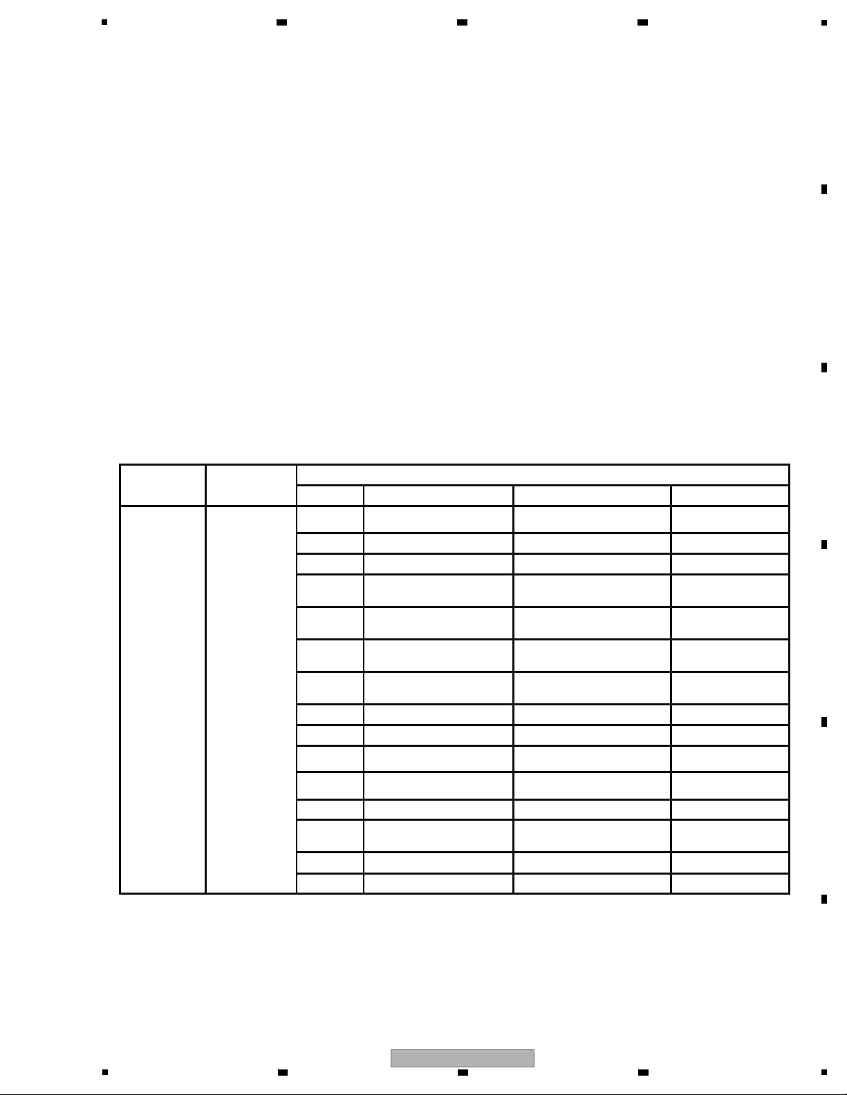
ASSY NAME
PCB ASSY
Part No.
Ref No. FUNCTION Part No. Remarks
IC101 MAIN CPU UPD61283F1-407LU2A
BGA
IC903 HDMI RECEIVER SII9233ACTU IC with heat-pad
IC905 HDMI SWITCH SII9387CTU IC with heat-pad
IC1204
DIGIT AL V IDEO FORMA T
CONVERTER
88DE2750
BGA
IC1212
(MAIN)
DDR2-SDRAM H5PS5162GFR-S5C-K
BGA
IC1212
(SUB)
DDR2-SDRAM K4T51163QI-HCE7
BGA
JA1501
CONNECTOR
(f o r BLUE TOOTH)
CKS5712-A
Land is under parts
IC1602 HDMI TRANSMITTER SII9136CTU IC with heat-pad
IC1603 HDMI TRANSMITTER SII9136CTU IC with heat-pad
IC9002 DSP D810K013BZKB400-K
BGA
IC9204 MEDIA PROCESSOR DM860
BGA
IC9203 LAN PHY LAN8700C-AEZG IC with heat-pad
IC9205 FLASH ROM AYW7346-A
MAC Address
closed-door
IC9510 REGULATOR NJM2846DL3-33 IC with heat-pad
DIGITAL MAIN
ASSY
AWX9825
(VSX-53)
(VSX-1326-K)
AWX9826
(VSX-52)
(VSX- 1126-K)
(VSX- 1121-K)
IC9509 REGULATOR MM1701WH IC with heat-pad
• Discharging
Please refer to page 43, “Preparations Before Perfoming Diagnosis of the POWER AMP Assy”.
• Ground Points
Please refer to page 44, “Ground Points”.
6 7 8
1. SERVICE PRECAUTIONS
1.1 NOTES ON SOLDERING
1.2 NOTES ON REPLACING
A
B
1.3 CAUTION
C
D
E
5
6 7 8
VSX-53
F
5
Page 6

1
Amplifier section
Continuous average power output of 110
watts* per channel, min., at 8 ohms, from 20
Hz to 20 000 Hz with no more than 0.08 %**
total harmonic distortion.
Continuous Power Output
(20 Hz to 20 kHz, 8 Ω, 0.08 %)
Front .................................... 110 W + 110 W
Center..................................................110 W
Surround ............................. 110 W + 110 W
Surround back (Front height/wide)
..............................................110 W + 110 W
Continuous Power Output (1 kHz, 6 Ω, 1.0 %)
Front ....................................150 W + 150 W
Center..................................................150 W
Surround .............................150 W + 150 W
Surround back (Front height/wide)
..............................................150 W + 150 W
Total harmonic distortion ......................... 0.06 %
(20 Hz to 20 kHz, 100 W + 100 W, 8 Ω )
Guaranteed speaker impedance ..... 16 Ω to 8 Ω,
less than 8 Ω to 6 Ω (setting required)
* Measured pursuant to the Federal Trade
Commission’s Trade Regulation rule on Power
Output Claims for Amplifiers
** Measured by Audio Spectrum Analyzer
Audio Section
Input (Sensitivity/Impedance)
LINE........................................ 350 mV/47 kΩ
Output (Level/Impedance)
REC........................................335 mV/2.2 kΩ
Signal-to-Noise Ratio
(IHF, short circuited, A network)
LINE
....................................................
103 dB
Frequency Response ....5 Hz to 100 000 Hz
dB
(Pure Direct Mode)
Tuner Section
Frequency Range (FM)
.....87.5 MHz to 108 MHz
Antenna Input (FM).................75 Ω unbalanced
Frequency Range (AM)
.......531 kHz to 1602 kHz
Antenna (AM) .............Loop antenna (balanced)
Video Section
Signal level
Composite Video
......................1 Vp-p (75 Ω)
Component Video
............Y: 1.0 Vp-p (75 Ω),
PB/PR: 0.7 Vp-p (75 Ω)
Corresponding maximum resolution
Component Video ..................1080p (1125p)
(Video convert off)
Digital In/Out Section
HDMI terminal ...........................19-pin (Not DVI)
HDMI output type................................5 V, 55 mA
USB terminal ...........USB2.0 Full Speed (Type A)
iPod terminal ........USB, and Video (Composite)
SIRIUS antenna cable.........8-pin mini DIN cable
ADAPTER PORT terminal.................5 V, 100 mA
WIRELESS LAN ADAPTER terminal
...........................................................5 V, 600 mA
Integrated Control Section
Control (SR) terminal
........
ø 3.5 Mini-jack (MONO)
Control (IR) terminal .........ø 3.5 Mini-jack (MONO)
IR signal.................High Active (High Level: 2.0 V)
12 V Trigger terminal ........ø 3.5 Mini-jack (MONO)
12 V Trigger output type...........12 V, Total 150 mA
RS-232C cable type.....................9-pin, cross type,
female-female
EXTENSION terminal ........................5 V, 150 mA
Network Section
LAN terminal ................10 BASE-T/100 BASE-TX
Miscellaneous
Power requirements ..................AC 120 V, 60 Hz
Power consumption ...................................570 W
In standby
............0.1 W (HDMI Setup – Control : OFF)
.............0.3 W (HDMI Setup – Control : ON)
Dimensions
....... 435 mm (W) x 185.6 mm (H) x 440.3 mm (D)
(17 3/16 in. (W) x 7 5/16 in. (H) x 17 3/8 in. (D))
Weight (without package)
VSX-53...................................13
.9 kg (30.6 lb)
VSX-52
...................................
13.7 kg (30.2 lb)
Number of Furnished Parts
MCACC Setup microp ho ne .........................1
Remote control unit ..................................1
AAA size IEC R03 dry cell batteries................2
iPod cable...................................................1
AM loop antenna ........................................1
FM wire antenna.........................................1
Warranty card ...........................................1
Power cord
CD-ROM (AVNavigator)
These operating instructions
Note
Specifications and the design are subject to
possible modifications without notice, due to
improvements.
This product includes FontAvenue
®
fonts
licensed by NEC Corporation. FontAvenue is a
registered trademark of NEC Corporation.
VSX-53 / VSX-52
2. SPECIFICATIONS
A
B
C
D
E
2 3 4
F
6
1
2 3 4
VSX-53
Page 7

5
Amplifier section
Continuous average power output of 110
watts* per channel, min., at 8 ohms, from 20
Hz to 20 000 Hz with no more than 0.08 %**
total harmonic distortion.
Continuous Power Output
(20 Hz to 20 kHz, 8 Ω, 0.08 %)
Front .................................... 110 W + 110 W
Center..................................................110 W
Surround ............................. 110 W + 110 W
Surround back (Front height/wide)
..............................................110 W + 110 W
Continuous Power Output (1 kHz, 6 Ω, 1.0 %)
Front ....................................150 W + 150 W
Center..................................................150 W
Surround .............................150 W + 150 W
Surround back (Front height/wide)
..............................................150 W + 150 W
Total harmonic distortion ......................... 0.06 %
(20 Hz to 20 kHz, 100 W + 100 W, 8 Ω )
Guaranteed speaker impedance ..... 16 Ω to 8 Ω,
less than 8 Ω to 6 Ω (setting required)
* Measured pursuant to the Federal Trade
Commission’s Trade Regulation rule on Power
Output Claims for Amplifiers
** Measured by Audio Spectrum Analyzer
Audio Section
Input (Sensitivity/Impedance)
LINE........................................ 350 mV/47 kΩ
Output (Level/Impedance)
REC........................................335 mV/2.2 kΩ
Signal-to-Noise R
atio
(IHF, short circuited, A network)
LINE
....................................................
103 dB
Frequency Response ....5 Hz to 100 000 Hz
dB
(Pure Direct Mode)
Tuner Section
Frequency Range (FM)
.....87.5 MHz to 108 MHz
Antenna Input (FM).................75 Ω
unbalanced
Frequency Range (AM)
.......531 kHz to 1602 kHz
Antenna (AM)
.............Loop antenna (balanced)
Video Section
Signal level
Composite Video
......................1 Vp-p (75 Ω)
Component Video
............Y: 1.0 Vp-p (75 Ω),
PB/PR: 0.7 Vp-p (75 Ω)
Corresponding maximum resolution
Component Video. ..................1080p (1125p)
(Video convert off)
Digital In/Out Section
HDMI terminal ...........................19-pin (Not DVI)
HDMI output type................................5 V, 55 mA
USB terminal ...........USB2.0 Full Speed (Type A)
iPod terminal ........USB, and Video (Composite)
SIRIUS antenna cable.........8-pin mini DIN cable
ADAPTER PORT terminal.................5 V, 100 mA
WIRELESS LAN ADAPTER terminal
...........................................................5 V, 600 mA
Integrated Control Section
Control (SR) terminal
.......
ø 3.5 Mini-jack (MONO)
Control (IR) terminal ........ø 3.5 Mini-jack (MONO)
IR signal.................High Active (High Level: 2.0 V)
RS-232C cable type. ..................9-pin, cross type,
female-female
EXTENSION terminal ........................5 V, 150 mA
Network Section
LAN terminal ................10 BASE-T/100 BASE-TX
Miscellaneous
Power requirements ..................AC 120 V, 60 Hz
Power consumption ...................................570 W
In standby
............0.1 W (HDMI Setup – Control : OFF)
.............0.3 W (HDMI Setup – Control : ON)
Dimensions
....... 435 mm (W) x 185.6 mm (H) x 440.3 mm (D)
(17 3/16 in. (W) x 7 5/16 in. (H) x 17 3/8 in. (D))
Weight (without package)
VSX-1326...............................13.9 kg (30.6 lb)
VSX-1126...............................13.7 kg (30.2 lb)
Number of Furnished Parts
MCACC Se
t
up mi cr opho ne.........................1
Remote control unit..................................1
AAA size IEC R03 dry cell batteries ...............2
iPod cable .................................................1
AM loop antenna .......................................1
FM wire antenna .......................................1
Power cord
CD-ROM (AVNavigator)
These operating instructions
Note
Specifications and the design are subject to
possible modifications without notice, due to
improvements.
This product includes FontAvenue
®
fonts
licensed by NEC Corporation. FontAvenue is a
registered trademark of NEC Corporation.
VSX-1326 only :
12 V Trigger terminal ...... ø 3.5 Mini-jack (MONO)
12 V Trigger output type..........12 V, Total 150 mA
VSX-1326-K / VSX-1126-K
6 7 8
A
B
C
D
E
F
VSX-53
5
6 7 8
7
Page 8

1
Amplifier section
Continuous average power output of 110
watts* per channel, min., at 8 ohms, from 20
Hz to 20 000 Hz with no more than 0.08 %**
total harmonic distortion.
Continuous Power Output
(20 Hz to 20 kHz, 8 Ω, 0.08 %)
Front. ....................................110 W + 110 W
Center..................................................110 W
Surround ............................. 110 W + 110 W
Surround back (Front height/wide)
..............................................110 W + 110 W
Continuous Power Output (1 kHz, 6 Ω, 1.0 %)
Front ....................................150 W + 150 W
Center..................................................150 W
Surround .............................150 W + 150 W
Surround back (Front height/wide)
..............................................150 W + 150 W
Total harmonic distortion ......................... 0.06 %
(20 Hz to 20 kHz, 100 W + 100 W, 8 Ω )
Guaranteed speaker impedance ..... 16 Ω to 8 Ω,
less than 8 Ω to 6 Ω (setting required)
* Measured pursuant to the Federal Trade
Commission’s Trade Regulation rule on Power
Output Claims for Amplifiers
** Measured by Audio Spectrum Analyzer
Audio Section
Input (Sensitivity/Impedance)
LINE........................................ 350 mV/47 kΩ
Output (Level/Impedance)
REC. ........................................335 mV/2.2 kΩ
Signa
l-to-Noise Ratio
(IHF, short circuited, A network)
LINE.
....................................................
103 dB
Frequency Response ....5 Hz to 100 000 Hz
dB
(Pure Direct Mode)
Tuner Section
Frequency Range (FM).....87.5 MHz to 108 MHz
Antenna Input (FM).................75 Ω unbalanced
Frequency Range (AM) .......531 kHz to 1602 kHz
Antenna (AM) .............Loop antenna (balanced)
Video Section
Signal level
Composite Video......................1 Vp-p (75 Ω)
Component Video ............Y: 1.0 Vp-p (75 Ω),
PB/PR: 0.7 Vp-p (75 Ω)
Corresponding maximum resolution
Component Video. ..................1080p (1125p)
(Video convert off)
Digital In/Out Section
HDMI terminal ...........................19-pin (Not DVI)
HDMI output type................................5 V, 55 mA
USB terminal ...........USB2.0 Full Speed (Type A)
iPod terminal ........USB, and Video (Composite)
SIRIUS antenna cable.........8-pin mini DIN cable
ADAPTER PORT terminal.................5 V, 100 mA
WIRELESS LAN ADAPTER terminal
...........................................................5 V, 600 mA
Integrated Control Section
Control (SR) terminal
.......
ø 3.5 Mini-jack (MONO)
Control (IR) terminal ........ø 3.5 Mini-jack (MONO)
IR signal.................High Active (High Level: 2.0 V)
RS-232C cable type....................9-pin, cross type,
female-female
EXTENSION terminal ........................5 V, 150 mA
Network Section
LAN terminal ................10 BASE-T/100 BASE-TX
Miscellaneous
Power requirements ..................AC 120 V, 60 Hz
Power consumption ...................................570 W
In standby
............0.1 W (HDMI Setup – Control : OFF)
.............0.3 W (HDMI Setup – Control : ON)
Dimensions
....... 435 mm (W) x 185.6 mm (H) x 440.3 mm (D)
(17 3/16 in. (W) x 7 5/16 in. (H) x 17 3/8 in. (D))
Weight (without package).............13.7 kg (30.2 lb)
Number of Furnished Parts
MCACC Setup microp ho ne .........................1
Remote control unit. ..................................1
AAA size IEC R03 dry cell batteries................2
iPod cable.
...................................................1
AM loop
antenna ........................................1
FM wire antenna ........................................1
Power cord
CD-ROM (AVNavigator)
These operating instructions
Note
Specifications and the design are subject to
possible modifications without notice, due to
improvements.
This product includes FontAvenue
®
fonts
licensed by NEC Corporation. FontAvenue is a
registered trademark of NEC Corporation.
VSX-1121-K
A
B
C
D
E
2 3 4
F
8
1
2 3 4
VSX-53
Page 9

5
Item to be checked regarding video Item to be checked regarding audio
Block noise Distortion
Horizontal noise Noise
Flicker Volume too low
Disturbed image (video jumpiness) Volume too high
Too dark Volume fluctuating
Too bright Sound interrupted
Mottled color
No. Procedures Check points
1
2
3
4
5
6
7
8
Confirm whether the customer complain has been solved.
If the customer complain occurs with the particular source,
such as Dolby Digital, DTS, AAC, DVD-A and HDMI, input it for
the operation check.
The customer complain must not be reappeared.
Video, Audio and operations must be normal.
Check the analog audio playback.
(Make the analog connections with a DVD player.)
Each channel audio and operations must be normal.
Check the digital audio playback.
(Make the digital connections with a DVD player.)
Each channel audio and operations must be nor
mal.
Check surround playback.
(Select Surround mode and check the multichannel operations
via the DSP circuit.)
Each channel audio and operations must be normal.
Check the tuner (AM and FM) operations. Audio and operations must be normal.
Check the video outputs.
(Connect with a DVD player.)
Video and operations must be normal.
Check the sound from headphone output. Sound must be normal, without noise.
Check the appearance of the product. No scratches or dirt on its appearance after receiving it for
service.
Items to be checked after servicing
To keep the product quality after servicing, confirm recommended check points shown below.
See the table below for the items to be checked regarding video and audio.
6 7 8
3. BASIC ITEMS FOR SERVICE
3.1 CHECK POINTS AFTER SERVICING
A
B
C
D
E
F
VSX-53
5
6 7 8
9
Page 10

1
H
POWER AMP ASSY
E
DIGITAL MAIN
ASSY
Q
CONNECT
ASSY
D
COMPONENT
ASSY
Z
BIND L BACK
ASSY
L
USB RECT
ASSY
B
COMPOSITE ASSY
C
DAC LOW ASSY
K
PRIMARY
ASSY
BIND R FRONT
ASSY
AA
FFC GUARD
ASSY
AC
FFC GUARD 2
ASSY
AD
V
POSI 1 ASSY
X
POSI 3 ASSY
W
POSI 2 ASSY
AE
BIND R BACK
ASSY
R
A-DAC BRIDGE
ASSY
I
PRESTAGE ASSY
BIND DISP FFC
ASSY
AB
AUDIO ASSY
A
M
REGULATOR
ASSY
U
MIC CONNECT
ASSY
Y
BIND L FRONT
ASSY
S
D-AUDIO BRIDGE
ASSY
T
D-DAC BRIDGE
ASSY
3.2 PCB LOCATIONS
A
2 3 4
B
C
D
E
F
10
VSX-53
1
2 3 4
Page 11

5
O
ENCODER ASSY
N
POWER SW
ASSY
J
DISPLAY ASSY
F
VOL ASSY
G
FRONT HDMI USB ASSY
P
MIC HP ASSY
NOTES: - Parts marked by “NSP” are generally unavailable because they are not in our Master Spare Parts List.
-
The > mark found on some component parts indicates the importance of the safety factor of the part.
Therefore, when replacing, be sure to use parts of identical designation.
6 7 8
A
B
Mark No. Description Part No.
LIST OF ASSEMBLIES
NSP 1..LOCAL POWER ASSY AWM8247
2..REGULATOR ASSY AWX9774
2..PRESTAGE ASSY AWX9775
2..USB RECT ASSY AWX9776
2..BIND R FRONT ASSY AWX9778
2..BIND L BACK ASSY AWX9779
2..BIND DISP FFC ASSY AWX9780
NSP 2..FFC GUARD ASSY AWX9777
NSP 2..FFC GUARD 2 ASSY AWX9892
NSP 1..COMPLEX ASSY(VSX-53/52) AWM8248
2..DISPLAY ASSY AWX9782
2..POWER SW ASSY AWX9783
2..ENCODER ASSY AWX9784
2..MIC HP ASSY AWX9785
2..PRIMARY ASSY AWX9786
2..VOL ASSY AWX9788
2..CONNECT ASSY AWX9878
NSP 1..COMPLEX ASSY
2..DISPLAY ASSY AWX9839
2..POWER SW ASSY AWX9900
2..ENCODER ASSY AWX9784
2..MIC HP ASSY AWX9785
2..PRIMARY ASSY AWX9786
2..VOL ASSY AWX9788
2..CONNECT ASSY AWX9878
NSP 1..AMP ASSY(VSX-53/1326-K) AWM8270
2..POSI 1 ASSY AWX9879
2..POSI 2 ASSY AWX9882
2..POSI 3 ASSY AWX9884
2..POWER AMP ASSY AWX9886
2..BIND L FRONT ASSY AWX9891
NSP 2..BIND R BACK ASSY AWX9586
(VSX-1326-K/1126-K/1121-K)
AWM8254
Mark No. Description Part No.
NSP 1..AMP ASSY(VSX-1126-K/1121-K) AWM8275
2..POSI 1 ASSY AWX9879
2..POSI 2 ASSY AWX9882
2..POSI 3 ASSY AWX9884
2..POWER AMP ASSY AWX9890
2..BIND L FRONT ASSY AWX9891
NSP 2..BIND R BACK ASSY AWX9586
NSP 1..AUDIO COMPOSITE ASSY
2..AUDIO ASSY AWX9767
2..COMPOSITE ASSY AWX9768
2..D-AUDIO BRIDGE ASSY AWX9769
2..D-DAC BRIDGE ASSY AWX9770
2..A-DAC BRIDGE ASSY AWX9771
2..MIC CONNECT ASSY AWX9772
NSP 1..
AUDIO COMPOSITE ASSY
2..AUDIO ASSY AWX9830
2..COMPOSITE ASSY AWX9768
2..D-AUDIO BRIDGE ASSY AWX9769
2..D-DAC BRIDGE ASSY AWX9770
2..A-DAC BRIDGE ASSY AWX9771
2..MIC CONNECT ASSY AWX9772
1..DAC LOW ASSY AWX9773
1..DIGITAL MAIN ASSY(VSX-53/1326-K) AWX9825
1..DIGITAL MAIN ASSY
1..COMPONENT ASSY AWX9864
1..FRONT HDMI USB ASSY AWX9897
1..FM/AM TUNER UNIT AXX7282
(VSX-53/1326-K)
(VSX-52/1126-K/1121-K)
(VSX-52/1126-K/1121-K)
AWR7102
AWR7105
AWX9826
C
D
E
NSP 1..AMP ASSY(VSX-52) AWM8274
2..POSI 1 ASSY AWX9879
2..POSI 2 ASSY AWX9882
2..POSI 3 ASSY AWX9884
2..POWER AMP ASSY AWX9889
2..BIND L FRONT ASSY AWX9891
NSP 2..BIND R BACK ASSY AWX9586
5
6 7 8
VSX-53
F
11
Page 12
1
[1] Jigs list
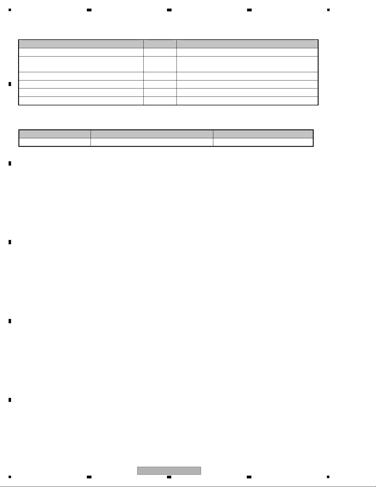
[2] Lubricants and Glues List
Name Lubricants and Glues No. Remarks
Silicone Grease GEM1057 Refer to “9.2 EXTERIOR SECTION”
Name Jig No. Remarks
19P FFC GGD1678 Diagnosis for POWER AMP ASSY, AUDIO ASSY
20P + 14P board to board extension jig cable GGD1759
Diagnosis for POWER AMP ASSY, AUDIO ASSY,
DIGITAL MAIN ASSY
20P + 20P board to board extension jig cable GGD1677 Diagnosis for DIGITAL MAIN ASSY
7P + 15P board to board extension jig cable GGD1762 Diagnosis for DIGITAL MAIN ASSY
30P board to board extension jig cable x 2 GGD1682 Diagnosis for DIGITAL MAIN ASSY, DAC LOW ASSY
28P + 14P board to board extension jig cable GGD1763 Diagnosis for DAC LOW ASSY
3.3 JIGS LIST
A
B
2 3 4
C
D
E
F
12
1
2 3 4
VSX-53
Page 13

5
6 7 8
A
B
C
D
E
F
VSX-53
5
6 7 8
13
Page 14

1
1.V-5_V
2.GNDV
3.V+5_V
4.GNDV
5.ZONE3_OUT
6.GNDV
7.ZONE2_OUT
8.GNDV
9.DVR_OUT
10.GNDV
11.MONITOR_OUT
12.GNDV
13.DVR_IN
14.GNDV
15.VIDEO_IN
16.GNDV
17.TV/SAT_IN
18.GNDV
19.DVD_IN
20.GNDV
20
2020
20
9/80
TUNER
MODULE
1.V+5_EV
2.POWLED
3.POWER KEY
4.GNDD
1.JOGA
2.JOGB
3.GNDD
39/380
1.AC1
2.AC2
3.VF
4.V+5_V
5.GNDV
6.GNDV
7.ACWP
4.XHPDET
3.HPR
2.GNDHP
1.HPL
*1.00mm
ADD7748-
ADD7751-
*1.00mm
CN8301 CN8302
CN3473
CN3001
JH3003JH3002
JP3002
CN2504
CN3601
CN8303
JP8403 CN8404
*3
EXCEPT
JXJ MODEL
JP3001
1.GNDD
2.CEC_FRONT
3.WP EDID
4.HPD
5.XVDDERR
CN3003
ADD7749-
5/60
5
CN8004
5.USBPOW
4.XUSBERR
3.D+
2.D-
1.GNDD
1.GNDD
2.CEC_IO
3.WP_EDID
4.HOTDET5
5.XVDDERR
JA8003
19.V+5D
18.V+5F
17.GNDD
16.HDSDA5
15.HDSCL5
14.SDA_SINK
13.SCL_SINK
12.RFXC-
11.GNDD
10.RFXC+
9.RFX0-
8.GNDD
7.RFX0+
6.RFX1-
5.GNDD
4.RFX1+
3.RFX2-
2.GNDD
1.RFX2+
CN8101
3
CN2501
28
CN2502
14
CN3001
15
CN3901 CN2861
7
CN3902
3
CN3785
2814
CN3794CN3792
2814
CN3793CN3791
30
CN3783
2814
CN2104 CN2103
30
CN2101
CN3784
30
CN3361
20 10
CN3362
723
CN3363CN3364
715
CN3774CN3772
157
CN3773CN3771
157 30
2020 20 10
723
CN5804 CN5805
10.NC
9.NECK6
8.NECK8
7.RY VL
6.WATTS
5.NC
4.NC
3.NC
2.XOLERR
1.RY AF
20.RY CR
19.RY FH
18.RY B
17.XPROTECT
16.NC
15.XDCERR
14.GNDD
13.GNDD
12.12VTRG1
11.12VTRG2
10.12VERR
9.232POW
8.GNDD
7.IRIN
6.RMC
5.SRIN
4.V+5R6_EV
3.V+5R6_EV
2.GNDD
1.GNDD
1.V+12_RY
2.V-12_RY
3.GND_TRG
4.GND_TRG
5.V+12V_TRG
6.NECK6
7.NECK8
8.RY VL
9.WATTS
10.XOLERR
11.RY AF
12.RY CR
13.RY FH
14.RY B
15.XPROTECT
16.XDCERR
17.GNDD
18.GNDD
19.12VTRG1
20.12VTRG2
21.12VERR
22.232POW
23.GNDD
1.IR IN
2.RMC
3.SR IN
4.V+5R6_EV
5.V+5R6_EV
6.GNDD
7.GNDD
*1.00mm
1.MICOUT
2.GNDA
3.V+7_A
4.GNDA
5.GNDA
6.V-7_A
7.MICDET
CN603CN602
1.NC
2.SBMUTE
3.AMUTE
3.BT L
2.GNDD
1.BT R
28.GNDADS
27.FR IN
26.GNDADS
25.FL IN
24.GNDADS
23.FR OUT
22.GNDADS
21.FL OUT
20.GNDDAS
19.SW OUT
18.GNDDAS
17.C OUT
1.GNDD
2.GNDD
3.VLSCK
4.VLSO
5.Z2VLSO
6.Z3MUTE
7.Z2MUTE
8.SBMUTE
9.AMUTE
10.PRESEL(F/XB)
11.LSSN
12.XMICDET5
13.RYHP
14.XHPDET
15.FHMUTE
1.TURST
2.TUSDA
3.TUSCL
4.TUIREQ
5.NC
6.GNDT
7.TR
8.V+5T
9.TL
14.SIRIUS L
13.GNDSI
12.SIRIUS R
11.GNDSI
10.V+5_AD
9.V+5_AD
8.GNDAD
7.GNDAD
6.V+12_A
5.V+12_A
4.GNDA
3.GNDA
2.V-12_A
1.V-12_A
1.BT L
2.GNDD
3.BT R
4.GNDD
5.XSIRST
6.SIRX
7.SITX
8.V+3R3_D
9.V+3R3_D
10.GNDD
11.GNDD
12.V+5_D
13.V+5_D
14.DIRPOW
15.DSPSO
16.DSPSCK
17.RYAC
18.ZDZF
19.XZ2DARST
20.XDARST
21.DACS
22.F96K
23.F192K
24.XADRST
25.XTLO
26.XDIRRST
27.DSPSI
28 DIRCS
1.BADA2.
SADA
3.CADA
4.FADA
5.DABCK
6.DALRCK
7.FLRCK
8.FBCK
9.FHADA
10.GNDD
11.DAMCK
12.GNDD
13.ZMCLK
14.GNDD
JA905 CN601 CN1503 CN1502 CN9002
CN1722CN1723
CN1501
5
*1.00mm
*1.00mm
*1.00mm
19/400
ADX7761-
ADX7768
5/480
30.BT L
1.DAZDB
15.GNDD
14.GNDD
2.XHPDET
1.FHMUTE
20.V+5R6_EV
19.V+5R6_EV
18.GNDD
17.GNDD
16.EV232RX
15.EV232TX
14.232CDET
13.232POW
12.GNDD
11.FANCTL
10.FANERR
9.XOSDRST
8.OSDCS
7.OSDSCK
6.OSDSO
5.SCL
4.SDA
3.CDET
2.V+5_V
1.V+5_V
7/175
PF07PG0S17
39.V+5R6_EV
38.V+5R6_EV
37.GNDD
36.GNDD
35.RMC
34.GNDD
33.IRIN
32.SRIN2
31.XOLERR
30.EVREQO
29.BTID
28.XEMRST5
27.BTDET
26.DVCPOWER
25.EVSI5
24.EVSO
23.EVSCK
22.EVREQI5
21.TEMPERR
20.EMPOW
19.LOWPOW
18.XSMUTE
17.HOTPLUG
16.CECIO
15.XVDDERR
14.XDCERR
13.NC
12.EV232RX
11.EV232TX
10.232EV
9.232POW
8.232CDET
7.NC
6.AMPTEMP
5.XFANERR
4.NC
3.HPD_F
2.WP_F
1.ACRY
4/550
D20PYY0455E
*2mm
JP3365
1.FRONTV
2.GNDCH
3.MICOUT
4.GNDA
5.V+7_A
6.GNDA
7.GNDA
8.V-7_A
9.MICDET
CN3471
ADX7763-
3/280
JH2505
7
CN6610CN6410
55
CN6110
5
CN6310
5
CN6510
5
CN6010
CN3651
JP4103_1
555 755
CN5310 CN5510CN5010CN5410 CN5610CN5110
2
CN605
3
CN606
2
CN604
2/75
PG02KA-F07
3/100
PG03KA-F10
2/100
PG02KA-F10
2.GNDD
1.POS2
3.GNDD
2.GNDD
1.POS3
2.GNDD
1.POS1
ADD7750-
7/310
JA8001 JA8101
JA3471JA3472
iPod VIDEO IN MIC IN
iPod Direct USBHDMI IN5
HEADPHONE IN
JA3476
FU10
!
*4
CN3002
for DBUG&D.L.
JA2506JA2505JA2504JA2502JA2501
JA2951(/H)
JA2952(/L)
L
R
CD-R/TAPE
INOUTCD
IN
DVR
INOUTVIDEO
IN
TV/SAT
ININ
DVDZONE2
OUT
ZONE3
OUT
JA8601
232C MONITOR IN2 IN1
OUT
(DVR) (DVD)
JA8301JA8304
PR
PB
YY
PB
PR
JA3605 JA3603 JA 3602 JA3601
DVD
ININ
TV/SAT
OUT
VIDEO
IN
ZONE2
OUTIN
MONITOR
OUT
DVRDVR
JA2003JA2002JA2008
OPT IN1 OPT IN2
COAX
IN1 IN2
JA2101
SIRIUS
CN7001 CN7003 CN7002
JP5723
JP5722
JP5723_1
JP5722_1
ADX7461-
ADX7461-
RF 5V OUT
JA5815
JA5804
SR IN
SR OUT
IR
JA5812IRJA5811IRJA5810
IN1 IN2 OUT
JA5807
12V TRG1
12V TRG2
FRONT
CENTER
SURROUND S-BACK F-HEIGHT/F-WIDE
RL RLRLRL
JA5800 JA5801 JA5802
JA906 JA901 JA907 JA902 JA904 JA1601 JA1602
BD IN IN1 IN2 IN3 IN5 OUT1 OUT2
JA9202
LAN
(UXJCB,CUXJ)
20.GNDV
19.GNDV
18.CVBSIN
17.GNDV
16.CV/SYOUT
15.GNDV
14.SCOUT
13.GNDV
12.CYOUT
11.GNDV
10.CBOUT
9.GNDV
8.CROUT
7.GNDV
6.CRIN
5.GNDV
4.CBIN
3.GNDV
2.CYIN
1.GNDV
1/140
1/140
J0052
J0054
J0055
J0056
J0057
J0058
JP2505
3
1.NC
2.FRONTV
3.GNDF
2.GNDUSB
1.V+UN_USB
1.RECMUTE
7.TUSCL
7.RECMUTE
6.TUIREQ
5.TUSENSE
4.TUADDR
3.TURST
2.TUSDA
1.TUSCL
CN3652
3.GNDCH
2.FRONTV
1.GNDCH
7.MICOUT
6.GNDA
5.V+7_A
4.GNDA
3.GNDA
2.V-7_A
1.MICDET
3
CN3651
CN3652CN3653
9.FRONTV
8.GNDF
7.MICOUT
6.GNDA
5.V+7_A
4.GNDA
3.GNDA
2.V-7_A
1.MICDET
1.VOLA
2.VOLB
3.GNDD
JH3004
JP8101
5.SBR
4.SBRIN2
3.SBRIN1
2 GAMP
5.FL
4.FLIN2
3.FLIN1
2.GAMP
1.GAMP
7.C
6.CIN2
5.CIN1
4.GAMP
3.GAMP
2.+VH
1.-VH
5.FR
4.FRIN2
3.FRIN1
2.GAMP
1.GAMP
5.SL
4.SLIN2
3.SLIN1
2.GAMP
1.GAMP
5.SR
4.SRIN2
3.SRIN1
2.GAMP
1.GAMP
JA903
IN4
1.USB_AC1
2.USB_AC2
IN6
ADD7748-
*1.25mm
9/80
2/120
ADX7760-
1.V+UN_USB
2.GNDUSB
SYXJ5
JXJ
DLPWXJ,FXJ,AXJ5
UXJCB,CUXJ
AXX7282-
*3
AXX7283-
-
TUNERMODEL
G
FRONT HDMI
USB ASSY
(AWX9897)
P
MIC HP ASSY (AWX9785)
J
DISPLAY ASSY
(VSX-53/52 : AWX9782)
(VSX-1326-K/1126-K
/1121-K : AWX9839)
U
MIC CONNECT
ASSY (AWX9772)
L
USB RECT ASSY
(AWX9776)
I
PRESTAGE ASSY (AWX9775)
V
POSI 1 ASSY
(AWX9879)
X
POSI 3 ASSY
(AWX9884)
W
P
(A
Q
CONNECT ASSY
(AWX9878)
B
COMPOSITE ASSY
(AWX9768)
D
COMPONENT
ASSY
(AWX9864)
H
POWER AMP ASSY
(VSX-53/1326-K : AWX9886)
(VSX-52 : AWX9889)
(VSX-1126-K/1121-K : AWX9890)
R
A-DAC BRIDGE ASSY
(AWX9771)
S
D-AUDIO BRIDGE ASSY
(AWX9769)
AUDIO ASSY
(VSX-53/1326-K : A
(VSX-52/1126-K/1121-K : A
AA
AB
BIND R FRONT ASSY
(AWX9778)
BIND DISP FFC ASSY
(AWX9780)
E
DIGITAL MAIN ASSY
(VSX-53/1326-K : AWX98
(VSX-52/1126-K/1121-K : AWX98
Y
Z
BIND L FRONT ASSY
(AWX9891)
BIND L BACK ASSY
(AWX9779)
()
E 1/10- E 10/10
H 1/2- H 2/2
()
2 3 4
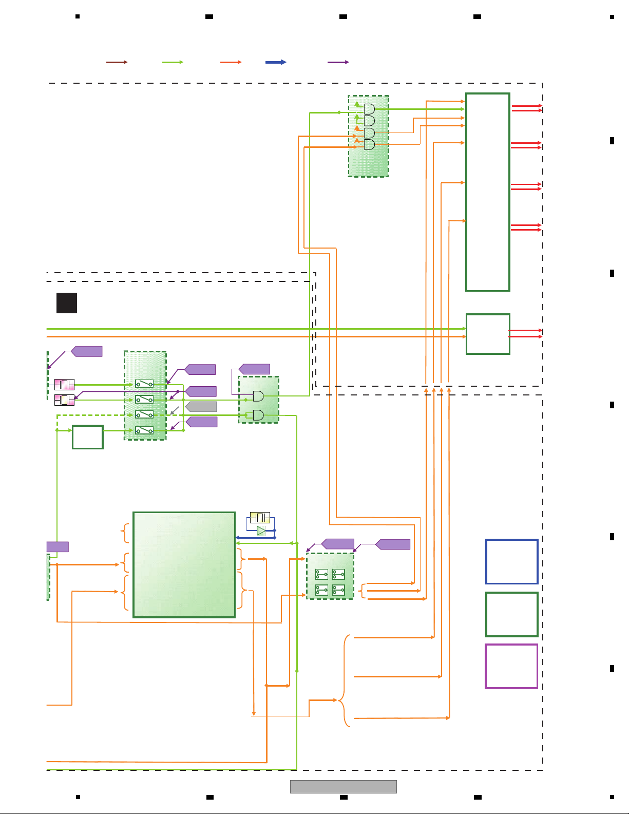
4. BLOCK DIAGRAM
4.1 OVERALL WIRING DIAGRAM
A
B
C
D
E
F
1
2 3 4
14
VSX-53
Page 15

5
!
!
AC CORD
SECONDARY
PRIMARY
MAIN TRANS
3/100
1.V+5_EV
2.POWLED
3.POWER KEY
4.GNDD
*2mm
1.JOGA
2.JOGB
3.GNDD
4/100
6
3.VF
4.V+5_V
5.GNDV
6.GNDV
7.ACWP
FAN
POWER AMP
A-REGV-REG
USB_RECT
!
FU7!FU6
PF06PG-S52
6/525
D20PYY0410E
D20PYY0310E
!
JH3003JH3002
CN3052
CN4102
CN4002
*1
*4
JXJ
!
*4
FU6,FU7 FU8,FU9
FXJ
(1.25A/125V)
REK1143-
AEK7072-
XXM3012-
MODEL
ATS7443-
ATS7445-
AC CORD
MAIN TRANS
*1
UXJCB
JXJ
DLPWXJ
AXJ5
FXJ
SYXJ5
!
ATS7444-
ADG7111-
BOARD IN
FFC
2.0mm FLAT CABLE
FFC CONNECTOR
2.0mm CABLE HOLDER
*2mm
XDG3061ADG7076XDG3061ADG7105XDG3032-
BOARD TO BOARD
T1501
AEK7075(T1.6A L/250V)
(1.6A/125V)
REK1144-
FU1 FU4
REK1154-
DEK1045-
(10A/125V)
(T10A L/250V)
REK1139(T2A H/250V)
REK1139(T2A H/250V) (T800mA L/250V)
CAUTION - FOR CONTINUED PROTECTION AGAINST RISK OF FIRE,
REPLACE WITH SAME TYPE AND RATINGS OF FUSE.
with same parts(safety regulation authorized) of identical
The mark found on some component parts should be replaced
designation.
CN4001
CN4101
CN83
CN82
RL1,RL1',RL7
RL4,RL5,RL8,RL9,RL10
RL2,RL3
RL6
UL TUBE
6
JP3001
ANOTHER CONNECTOR
CN3401 CN3501
DLPWXJ,FXJ
UXJCB,CUXJ
J3003
J3002
3
CN2501
28
CN2502
3
CN3785
28
CN3794
28
CN3793
3030
CN3783 CN3781
28
CN2103
30 30
CN2101 CN2102
CN3784
30 30
CN3782
3030
V-REG
A-REG
1.NC
2.SBMUTE
3.AMUTE
4.GNDA
5.GNDA
6.RS OUT
7.GNDA
8.LS OUT
9.GNDA
10.FR OUT
11.GNDA
12.C OUT
13.GNDA
14.FL OUT
15.GNDA
16.SB/FH R OUT
17.GNDA
18.SB/FH L OUT
19.GNDA
3.BT L
2.GNDD
1.BT R
28.GNDADS
27.FR IN
26.GNDADS
25.FL IN
24.GNDADS
23.FR OUT
22.GNDADS
21.FL OUT
20.GNDDAS
19.SW OUT
18.GNDDAS
17.C OUT
16.GNDDAS
15.SR OUT
14.GNDDAS
13.SL OUT
12.GNDDAS
11.SBR/FHR OUT
10.GNDDAS
9.SBL/FHL OUT
8.GNDDAS
7.NC
6.GNDDAS
5.NC
4.GNDDAS
3.ZR OUT
2.GNDDAS
1.ZL OUT
5.V+12_A
4.GNDA
3.GND
A
2.V
-12_A
1.V-12_A
7.SITX
8.V+3R3_D
9.V+3R3_D
10.GNDD
11.GNDD
12.V+5_D
13.V+5_D
14.DIRPOW
15.DSPSO
16.DSPSCK
17.RYAC
18.ZDZF
19.XZ2DARST
20.XDARST
21.DACS
22.F96K
23.F192K
24.XADRST
25.XTLO
26.XDIRRST
27.DSPSI
28.DIRCS
29.UNLK
30.DAZDB
1.BADA
2.SADA
3.CADA
4.FADA
5.DABCK
6.DALRCK
7.FLRCK
8.FBCK
9.FHADA
10.GNDD
11.DAMCK
12.GNDD
13.ZMCLK
14.GNDD
15.ZBCK
16.ZFADA
17.ZLRCK
18.GNDD
19.DIRMCKO
20.GNDD
21.DIRLRCK
22.DIRDATO
23.DIRINT
24.DAC0DET
25.GNDD
26.DIRMCKI
27.GNDD
28.DIRBCK
29.GNDD
30.MSPDIF
HDMI CONNECTOR
CN9002 CN9003
CN9501
CN4081
3
1.V+5_V
2.GNDV
3.GNDV
4.V-5_V
5.FANCTL
6.FANERR
30.BT L
1.DAZDB
30.BADA
1.MSPDIF
7
7.RYAC
6.GNDD
5.GNDD
4.GNDD
3.V+5R6_EV
2.V+5R6_EV
1.V+5R6_EV
ADX7762-
7/180
JP51
3.V+FAN
2.V-FAN
1.LOCK DET
1.GNDAD
2.V+5_AD
3.V+12_A
4.GNDA
5.GNDA
6.V-12_A
7/175
PF07PG0S17
4.GNDTRG
3.V+12_TRG
2.V-12_A
1.V+12_A
1.ACWP
2.GNDD
3.GNDD
4.V+5R6_V
5.-VF
6.AC2
7.AC1
CN4052
7
!
FU8!FU9
*4
PF06PG-S47
6/475
5
CN6510
5
CN6010
5
CN6210
CN6603
ADD7730-
19/50
reverse
555
CN5510 CN5210CN5010
CN5701
CN606
2
2/100
PG02KA-F10
2.GNDD
1.POS2
PIN JACK
JA71 YEL
JA71_1 WHT
*4
FU4
!
*4
FU1
!
CN81
CN84
(DLPWXJ,FXJ,AXJ5)
JP3701_1
JP3704_1
JP3705_1
JP3706_1
JP3703_1
JP3702_1
AXJ5
SYXJ5
DLPWXJ,FXJ
AXJ5
ORG
JP81_1
JP81
JP81_2
JP81_3
(UXJCB,CUXJ,JXJ)
(SYXJ5)
(DLPWXJ,FXJ,AXJ5)
(DLPWXJ,AXJ5)
(FXJ)
BRN
(DLPWXJ,AXJ5)
(FXJ)
GRN
BLU
(DLPWXJ,AXJ5)
(FXJ)
YEL
RED
(FXJ)
(DLPWXJ,AXJ5)
2VOLT SW-L ASSY
2VOLT SW-H ASSY
CN3711
(FXJ)
(DLPWXJ,AXJ5)
JP3704
JP3701
JP3702
JP3703
JP3706
JP3705
ORG
BRN
GRN
BLU
YEL
RED
CUXJ
(DLPWXJ,SYXJ5)
FU10MODEL
VSX-53
VSX-52
VSX-LX55
VSX-1326-K
VSX-1126-K
VSA-LX55
UXJCB
CUXJ
UXJCB
CUXJ
SYXJ5
DLPWXJ
VSX-1121-K
AXJ5
(4A/125V)
REK1149-
(10A/125V) (1.6A/125V)
REK1144-REK1154- REK1143-
(1.25A/125V)
REK1139(T2A H/250V)
(1.25A/125V)
REK1154- REK1143-
(10A/125V) (T2A H/250V)
REK1139- REK1144-
(1.6A/125V)
(T4A H/250V)
AEK7075(T1.6A L/250V)
AEK1061-
(T800mA L/250V)
AEK7072-
(T5A L/250V)
REK1104- AEK1059-
(T3.15A L/250V)
VSX-LX55
VSX-LX55
VSX-LX55
VSA-LX55
VSX-53
VSX-1126-K
VSX-52
VSX-1121-K
VSX-1326-K
JA3201JA3101JA2506JA2505
FH/FW
PRE OUT
SBS
L
R
L
R
C&SWF
CD-R/TAPE
INOUTCD
IN
JA2006JA2004JA2003JA2002JA2008
OPT OUT1OPT IN1 OPT IN2 OPT IN3
COAX
IN1 IN2
CN7002
JA1602
OUT2
JA9202
LAN
JA9301
BT ADAPTER
PORT
DB416NB2
DB118NB2
DB217NB2
DB320NB2
DB618NB2
DB522NB2
ATS7442- ADG7111-
1/160
1/180
1/170
1/200
1/180
1/220
ADX7737-
J0053
VSX-LX55
VSX-2021-K
VSX-2021-K
VSX-LX55
DLPWXJ
VSX-LX55
VSX-53
AXJ5
UXJCB
CUXJ
JXJ
FXJ
VSX-52
VSX-1326-K
MICROPHONE
MODEL
REMO-COM
*OPTION
AXD7613-
iPod CABLE
APM7010-
VSX-1121-K
VSX-1126-K
VSX-2021-K
VSA-LX55
APM7010- AXD7612- -
APM7010- AXD7613--
APM7010- AXD7614- ADE7136- -
SYXJ5
VSX-LX55
4/600
PF04PG-S60
AXD7613-APM7010-SYXJ5
-
(FXJ)
(FXJ)
SHIELD CABLE
4
*2mm
1.VOLA
2.VOLB
3.GNDD
CN3371
D20PYY0310E
J3004
3/100
JH3004
5.SBL
4.SBLIN2
3.SBLIN1
2.GAMP
1.GAMP
5.SBR
4.SBRIN2
3.SBRIN1
2.GAMP
1.GAMP
5.FL
4.FLIN2
3.FLIN1
2.GAMP
1.GAMP
7.VH_b
6.VL-H_b
5.VL-L_b
4.GND
3.VL-L_a
2.VL-H_a
1.VH_a
6.VIDEO_AC2
5.VIDEO_G
4.VIDEO_AC1
3.NC
2.FL_AC2
1.FL_AC1
1.AUDIO_AC1
2.NC
3.AUDIO_G
4.NC
5.AUDIO_AC2
CN4103
USB
JA9201
*1.25mm
4/170
JA71 ADX7771- /J ONLY
ADX7772- /OTHER
(4A/125V)
REK1149-
REK1149(4A/125V)
AEK1059(T3.15A L/250V)
ADE7136-
ADE7136-
ADE7136-
ADE7136-
WIFI CABLE
ADE7137-
ATS7442-
ATS7445-
ATS7445-
(No mount)
(No mount)
(No mount)
N
POWER SW ASSY
(VSX-53/52 : AWX9783)
(VSX-1326-K/1126-K/1121-K : AWX9900)
O
ENCODER ASSY
(AWX9784)
W
POSI 2 ASSY
(AWX9882)
C
DAC LOW ASSY
(AWX9773)
T
D-DAC BRIDGE
ASSY (AWX9770)
A
6-K : AWX9767)
6-K/1121-K : AWX9830)
K
PRIMARY ASSY
(AWX9786)
M
REGULATOR ASSY
(AWX9774)
AC
FFC GUARD ASSY
(AWX9777)
AD
AE
BIND R BACK ASSY
(AWX9586)
FFC GUARD 2 ASSY
(AWX9892)
Y
: AWX9825)
21-K : AWX9826)
()
()
A 1/3- A 3/3
C 1/2- C 2/2
)
10/10
When ordering service parts, be sure to refer to "EXPLODED VIEWS and PARTS
LIST" or "PCB PARTS LIST".
The mark found on some component parts indicates the importance of the safety
factor of the part. Therefore, when replacing, be sure to use parts of identical
designation.
: The power supply is shown with the marked box.
F
VOL ASSY (AWX9788)
6 7 8
A
B
C
D
E
5
6 7 8
VSX-53
F
15
Page 16

1
COAX2(CD)
IC9204
MNP
DM860
IC903
HDMI
RECEIVER
SII9233ACTU
OPT IN1(TV/SAT)
OPT IN2(DVR/BDR)
OPT IN3(VIDEO)
COAX1(DVD)
HDMI IN4
(VIDEO)
HDMI IN2
IC905
HDMI SWITCH
SII9387CTU
HDMI OUT1
IC9002
1st DSP
D810K013BZKB400
IC1604
BASIC AUDIO
SELECTOR
IC1602
HDMI
TRANSMITTER
SII9136CTU
IC2471
ZONE2 DAC
AK4388ET
TX1
LPF
JA907
JA901
JA2002
JA2003
JA2004
JA1601
JA2006
FRONT HDMI IN
DVR OUT
ZONE2 OUT
SW DownMix
JA8001
IC2701, IC2702
JA2951
JA2504
ZONE3 OUT
JA2951
HEADPHONE
<<AUDIO ZONE OUT>>
Sirius
JA2101
HDMI IN1
JA906
IC1603
HDMI
TRANSMITTER
SII9136CTU
JA1602
HDMI OUT2
NETWORK
JA9202
IC9203
ETHERNET
PHYCEIVER
LAN8700C-AEZG
S/PDIF
IC1816
DSP/2ch DIRECT
SELECTOR
I2S
I2S
S/PDIF
IC2451
(ZONE2)
LPF
S/PDIF
DSD(FR,SL)
I2S
(C,SW,SL,SR)
I2S(SBL,SBR)
DSD(C,SW,SR)
IC1809
S/PDIF
SELECTOR
I2S
I2S(FL,FR)
DSD(FL)
2ch PCM Only
I2S(FL,FR
A/D BUFFER
IC2401
NJM4565MD
NOTE
SPDIF:SONY/Philips Digital Interface
I2S:The Inter-IC Sound
USB
JA8101
IC8003
HDMI EQ
CXB1443R
IC1814
DIR(or USB)
/HDMI SELECTOR
IC1815
ZONE2
USB/NET
SELECTOR
OPT OUT1
I2S
DSD
BD
JA902
DSD(SL)
S/PDIF
S/PDIF
I2S(FL,FR)
DSD(FL)
I2S(except FL,FR)
JA2008
BT
IC101
MAIN LSI (EMMA)
UPD61283F1-407LU2A
IC2001
DIR&DIT
AK4118AEQ
S/PDIF
I2S
IC2431
ADC
PCM1804DB
I2S(DATA)
I2S(BCK,LRCK)
IC1817
DSD/PCM
SELECTOR
IC2201
DAC
PCM1691
IC2231(FL,FR)
IC2281(C,SW)
IC2331(SL,SR)
IC2381(SBL,SBR)
No mount
VSX-53/VSX-1326-K Only
HDMI IN5
(DVD)
JA903
HDMI IN6
(DVR/BDR)
JA904
I2S
JA1501
E
DIGITAL MAIN ASSY
C
DAC LOW ASSY
G
FRONT HDMI USB
ASSY
P
MIC HP ASSY
P
MIC HP ASSY
2 3 4
4.2 BLOCK DIAGRAM FOR AUDIO BLOCK
A
B
C
D
E
F
16
1
2 3 4
VSX-53
Page 17

5
FRONT HDMI IN
MIC
TV/SAT
VIDEO
CD
PHONO
PREOUT L/R
PREOUT SW1
PREOUT SL/SR
PREOUT SBL/SBR
DVR OUT
SP L/R
SP C
SP SL/SR
SP SBL/SBR
HP
SW DownMix
JA3471
JA8001
IC2701, IC2702
JA2502
JA2504
SW PRE Amp
IC2751
JA2504
JA3476
JA5800
JA5800
JA5801
JA5801
JA5802
JA3101
JA3101
JA3201
JA3201
PREOUT C
JA3101
DVD
DVR
JA2501
JA2501
ZONE3 OUT
JA2951
HEADPHONE
AMP
<<PREOUT>>
MIC Amp
IC3471
NJM4565MD
USB
JA8101
IC8003
HDMI EQ
CXB1443R
IC3101
IC3151
IC3201
IC3251
IC2801
NJM4565MD
JA2503
JA2503
PREOUT FHL/FHR
JA3201
IC3221
PRE SELECTOR
SP FHL/FHR
JA5802
RY5811,
RY5851
TUNER Module
IC3271
IC2501
Selector / Volume / PRE Amp
BD3473KS2
SW PRE Amp
IC2751
JA3102
PREOUT SW2
<<POWER AMP
INPUT BUFFER>>
<<POWER AMP>>
G
ASSY
P
MIC HP ASSY
A
AUDIO ASSY
I
PRESTAGE
ASSY
H
POWER AMP ASSY
P
MIC HP ASSY
6 7 8
A
B
C
5
D
E
VSX-53
F
17
6 7 8
Page 18

1
HDMI SW
Silicon Image
"SiI9387"
IC905
HDMI Rx
Silicon Image
"SiI9233ACTU"
IC903
Video Decoder
Analog Devices
"ADV7181C"
IC909
"UPD
Nor FLA
64Mb* 128M
Gate Array
SEIKO EPSON
"PE7008A"
IC603
LAN PHY
SMCS
"LAN8700"
IC9203
Media
Processor
BRIDGE CO
"DM860"
IC9204
SDRAM-166
128Mb(8Mx16)
FLASH ROM
64Mb(4Mx16)/90ns
36.864MHz
28.63636MHz
27MHz
HDMI IN4
HDMI IN3
HDMI BDIN
HDMI IN1
HDMI IN2
HDMI EQ
SONY
"CXB1443R"
HDMI
EDID
GU
COMPOSITE
COMPONENT
Pb
Pr
ETHERNET
CK:27M-148.5MHz
/DT:36bit/DE,VS,H
CK:27M
/DT:BT656
Only VDEC 480i output
CK:27MHz
/DT:BT656(8bit)
C
/
(DT:16b
CEC
ANALOG
VIDEO BLOCK
VBUSE2IN
VBUSMA
More than VDEC480p output
CK:27M-74.25MHz
/DT:16bit/DE,VS,HS
SD
VDE
Y
24.576 MHz
24MHz
25 MHz
HDMI IN5
G
FRONT HDMI USB ASSY
D
COMPONENT
ASSY
B
COMPOSITE
ASSY
2 3 4
4.3 BLOCK DIAGRAM FOR DIGITAL MAIN VIDEO BLOCK
A
B
C
D
E
F
18
1
2 3 4
VSX-53
Page 19

5
EMMA2RL2
NEC
"UPD61283F1-407LU2A"
IC101
IP.SCALER
Marvell
"88DE2750"
IC1204
HDMI Tx
Silicon Image
"SiI9136"
IC1602
HDMI Tx
Silicon Image
"SiI9136"
IC1603
DDR2-800
512Mb(32Mx16)
EVENT ucom
SANYO
"PDC188A8"
Nor FLASH
64Mb* 128Mb/90ns
iPod
Authentication
APPLE
(RENESAS)
"341S2164"
IC602
2
2
2
2
27MHz
20MHz
SD
VENC
USBuCOMGUI
COMPONENT-Y
COMPOSITE
COMPONENT-Pb
COMPONENT-Pr
USB(FRONT)
CK:27M
/DT:BT656
CK:27M-148.5MHz
/DT:36bit/DE,VS,HS
CK:27M-148.5MHz
/DT:36bit/DE,VS,HS
(DT:16bit)
CEC
HDMI OUT1
HDMI OUT2
POWER SUPPLY BLOCK Diagram
(DCDC,LDO)
TMDS
DIGITAL VIDEO
CEC
ANALOG VIDEO
CLOCK
DIGITAL AUDIO
VBUSMAIN
VBUSE2
I2C
SD
VDEC
DDR-333/400
256Mb(16Mx16)
CDCE925
(PDJ019A)
27MHz
24.576 MHz
48 MHz
ANALOG
VIDEO BLOCK
J
DISPLAY
ASSY
G
FRONT HDMI USB ASSY
B
COMPOSITE
ASSY
D
COMPONENT
ASSY
E
DIGITAL MAIN ASSY
6 7 8
A
B
C
5
VSX-53
6 7 8
D
E
F
19
Page 20

1
AND (SZ08)
IC1804
SEL (VHC125)
IC1817 1/2
SEL
(VHC125)
IC1817 2/2
SEL (VHCT125)
IC1809
DIR
IC2001
USB
EMMA
IC101
HDMI
TX
IC1602 (IC1603)
HDMI
RX
IC903
NMP
BCo
IC9204
COAX 1
COAX 2
OPT 1
OPT 2
XNET
ADC
IC2431
ZDB
IC1803
24.576MH
22.5792M
AMCLK
BCK
LRCK/DSDFR
FD/DSDFL
SD/DSDC
CD/DSDLFE
SPDIF/DSDS
BD/DSDSR
SD/DSDFR
--/DSDC
--/DSDLFE
CD/DSDSL
BD/DSDSR
HDMI-AMCLK
HDMI-I2S(LR)
USB-AMCLK
USB-I2S(LR)
THROUGH-I2S
SOURCE-I2S
(LR)
I2S DT(multi-c
SOURCE-AMCLK
XTI
MCKO1
BCK2
LRC K2
SDTO 2
DAUX
SEL (LCX157)
IC1815
SEL (LCX157)
IC1814
SEL (LCX157)
IC1604
XEMMASPDIF
XHARC
XHDSPDIF
DSDSW
XDSDS
XBAOUT
Z2ZNET
A:B:ZNET
HDI2S
A:/B:HDMI
27.0MHz
XXTL0
XZ2DAC
XS
SE
USB-AMCLK
USB-I2S(LR)
NMP-AMCLK
NMP-
CLOCK
GENERATOR
CDCE925
IC604
AND (SH08)
IC605
24MHz
24.576MHz
27.0MHz
MSPDIF
COAX 3
OPT 3
OPT 4
27MHz
SOURCE-I2S
(LR)
NETPOW
SOURCE/I2S(LR)
C
DAC LOW ASSY
E
DIGITA
2 3 4
4.4 BLOCK DIAGRAM FOR DIGITAL MAIN AUDIO BLOCK
A
B
C
D
E
F
20
VSX-53
1
2 3 4
Page 21
5
AND (WZ08)
IC1802
SEL
(VHC126)
IC1806
SPDIF
AMCLK I2S
1st D S P
D A 810
IC9002
AHCLKR0
ACLKR0
AFSR0
AXR0[0]
AHCLKR1
ACLKR1
AFSR1
AXR1[0]
AXR1[1]
AXR1[2]
AXR1[3]
AXR1[4]
AXR1[5]
AHCLKX
ACLKX
AFSX
AXR1[6]D1FDT
AXR1[7]D1CDT
AXR1[8]D1SDT
AXR1[9]D1BWDT
AXR1[10]D1HWDT
AXR1[11]D1DMDT
AMUTE
ZDB
IC1803
24.576MHz
22.5792MHz
SOURCE-I2S
THROUGH-I2S
I2S -BCK
I2S-LRCK
I2S-LR
I2S-SURR
I2S-C/LFE
I2S-SRB/HEIGHT
SOURCE-I2S
(LR)
I2S DT(multi-ch)
SYSCLK
DAMCLK
ZONE-I2S (LR)
ZONE-AMCLK
SEL (LCX157)
IC1816
20.0MHz
24PQLS
22PQLS
XPQLS
DAZDB
DACSIG
DSPPAS
SE
XDACSIG
XS
XXTL0
FLG
DAC
IC2201
I2S-LR
I2S-C/LFE
I2S-SURR
I2S-SRB/HEIGHT
Z2DAC
FL/FR
IC2471
AND
(LCX08)
IC2004
I2S-BCK
I2S-LRCK
SOURCE-I2S
(LR)
NETPOW
DIRPOW
DVCPOW
E
DIGITAL MAIN ASSY
6 7 8
A
B
C
D
5
VSX-53
6 7 8
E
F
21
Page 22

1
COMPOSITE VIDEO BLOCK DIAGRAM
IC8301
IC8401
IC8501
EMMA
COMPOSITE
INPUT
COMPOSITE
OUTPUT
VDEC
OSD IC
PDC162A
LPF
FRONT VIDEO
DVD
TV/SAT
VIDEO
DVR/BDR
VIDEO AMP
NJM2505AF
iPod
ZONE2 OUT
MONITOR OUT
DVR/BDR OUT
95949392918988
87
8382817977
757575
VIDEO SW
NJW1327FU1
96
E
DIGITAL MAIN ASSY
COMPONENT ASSY
D
2 3 4
4.5 BLOCK DIAGRAM FOR COMPOSITE VIDEO BLOCK
A
B
C
D
E
F
22
VSX-53
1
2 3 4
Page 23

5
I2C
IC8301
EMMA
IN 1
(DVD)
IN 2
(DVR/BDR)
MONITOR OUT
COMPONENT
INPUT
COMPONENT
OUTPUT
VCYOUT
VCBOUT
VCROUT
VDEC
LPF
LPF
LPF
CDET
LPF
LPF
LPF
VIDEO SW
NJW1327FU1
19
21
22
15
16
18
33
34
35
30
31
32
41
40
39
44
43
42
71
70
69
68
75
75
62
61
60
59
75
75
53
52
51
49
75
75
COMPONENT VIDEO BLOCK DIAGRAM
E
DIGITAL MAIN ASSY
COMPONENT ASSY
D
4.6 BLOCK DIAGRAM FOR COMPONENT VIDEO BLOCK
6 7 8
A
B
D
E
C
5
6 7 8
VSX-53
F
23
Page 24

1
Power Supply Block Diagram (SMPS Part)
SMPS
V+5R6_EV
V+5R6_DDD
DC-DC
DC-DC
2ch DC-DC
Controler
V+3R3_HHH
V+1R8_HHH
iPod IC
LDO
MAIN LSI
+ROM
+DDR-SDRAM
Video
Decoder
HDMI
Rx
LDO
Network LSI
+ROM+RAM
Network
PHY
V+3R3_NW
V+1R2_NW
V+3R3_EM
V+2R5_EM
LDO
V+1R05_EM
Gate Array
HDMI
SW
V+5_HD
HDMI
Cable EQ
LDO
+3.3V
LDO
V+1R2_RX
HDMI
Tx1
HDMI
Tx2
Load SW
HDMI OUT1 +5V
Load SW
Q9503
Scaler
+VRAM
LDO
V+1R8_SC
V+1_SC
V+1R8_DSP
MAIN Transformer
Other Circuits
AC Relay
RY71
IC9507
MB39C011A
IC9502
S-1172B12-U5
IC9508
S-1170B25UC-OTK
IC9509
MM1701WH
IC9511
S-1170B50UC-OUJ
IC9505
S-1172B12-U5
IC9501
S-1172B10-U5
Q601
IC1606
AAT4614AIGU-2
IC9503
IC8004
S-1132B33
CN9501
V+5R6_EV
IC9204
IC9201
IC9205
IC9203
IC101
IC402
IC403
IC404
IC603
IC602
IC909
IC905
JA905
IC903
IC1602
IC1603
JA1601
JA1602
HDMI OUT2 +5V
IC1605
AAT4614AIGU-2
IC1204
IC1212
IC8003
JA800
VSX-53
VSX-1326-K
VSX-52
Refer to
MAIN Transformer part
A
Q9501
Q9502
Q9505
LDO
IC9513
S-1170B50UC-OUJ
LDO Load SW
IC9202
BD2226G
JA9201
+5V for
Wireless LAN
Converter
V+5_WF
LDO
IC9506
S-1172B12-U5
V+1R2_TX
Clock
Generator
IC604
K
PRIMARY ASSY
G
FRONT HDMI USB ASSY
E
DIGITAL MAIN
ASSY
2 3 4
4.7 BLOCK DIAGRAM FOR POWER BLOCK(1)
A
B
C
D
E
F
24
1
VSX-53
2 3 4
Page 25

EVENT CPU
V+5_EV
Load SW
Q9503
Scaler
+VRAM
LDO
V+1R8_SC
V+1_SC
LDO
V+3R3_DS
LDO
V+1R2_D1
DSP
+ROM
+RAM
LDO
V+3R3_OS
OSC
24.576M
22.5792M
LDO
V+5_DSP
Logic for
Digital Audio
Load SW
DIR&DIT
OPT IO
RS232C
SR,IR
RYAC
DVCPOW
NETPOW
DIRPOW
232POW
BTPOW
IC9501
S-1172B10-U5
IC1606
AAT4614AIGU-2
from
EVENT CPU
from
MAIN LSI
/Gate Array
IC9503
S-1172B12-U5
IC9512
NJM2872BF33
IC9504
S-1170B50UC-OUJ
IC1505
BD2224G
Q8604
Q5971
Power Supply
Control Signals
JA160
HDMI OUT2 +5V
IC1204
IC1212
IC9510
NJM2846DL3-33
IC9002
IC9001
IC9003
IC9004
X1801
X1802
JA1501
BT Adaptor
CN9002
CN3784
CN3783
CN2101
IC2001
CN1722
CN8302
IC8601
CN602
CN601
JA5815
Power Supply for
Extention
CN3362
CN5804
CN3364
CN3001
FFC
IC3001
VSX-1326-K
VSX-52
WUSBPOW
V+5_D
V+3R3_D
Q
CONNECT ASSY
H
POWER AMP ASSY
J
DISPLAY ASSY
D
COMPONENT ASSY
C
DAC LOW
ASSY
T
D-DAC BRIDGE ASSY
5
6 7 8
A
B
C
D
E
VSX-53
5
6 7 8
F
25
Page 26

1
Power Supply Block Diagram (MAIN Transformer Part)
MAIN
Transformer
RECTIFIER
D5703
RECTIFIER
D5790,D5791
CN5701
VL+
VL-
7
RECTIFIER
D4101-4104
IC4101
NJM78M12FA
IC4102
NJM79M12FA
IC4021
NJM78M06FA
RECTIFIER
D4001
IC4001
NJM78M05FA
IC4001
NJM79M05FA
RECTIFIER
D4051-4053,C4051
RECTIFIER
D4125-4127,C4125
IC4121
NJM78M12FA
CN4101
3
3
CN4001
2
+
-
+
-
+
-
RECTIFIER
D4081,4082,C4081
+
Q4082
V+12A
V-12A
V+6AD
V+5V
V-5V
CN4081
FAN
CN4002
CN4052
AC1,AC2
-VF
V+5_V
CN4102
V+12TRG
No mount
2
for FL
Q3001
Q3002
Q3901
V
V
TUNER MODULE
CN3902
FFC
V+5_T
V-12_A
V+12_A
IC2183
NJM2845DL1-05
V+5_DA
IC2181
NJM2855DL1-33
V+3R3_DA
Q8401
Q8409
V+5_V
V-5_V
V+3_V
V-3_V
V+5_V
V-5_V
CN8303
CN3601
CN3001
CN3792
CN3791
CN2104
C
C
A
CN4103
Q5705
Q5707
J
DISP
M
REGULATOR ASSY
B
COMPOSITE AS
D
C
H
POWER AMP ASS
C
DAC LOW ASSY
R
A-DAC BRIDGE ASSY
A
AUDIO ASSY
2 3 4
4.8 BLOCK DIAGRAM FOR POWER BLOCK(2)
A
B
C
D
E
F
26
1
2 3 4
VSX-53
Page 27

5
AC1,AC2
-VF
V+5_V
RECTIFIER
D3651
+
V+5_USB
V-12A
V+12A
CN5805
CN3363
V+12TRG
for SP Relay
for FL
V+12_A
V-12_A
V+7_A
V-7_A
V+5_DA
V+3R3_DA
V+5_V
V-5_V
VH+
VH-
CN8303
CN3601
CN2504
CN3652
FFC
CN8302
CN1722
V+5_V
JA8101
USB +5V Supply
CN3651 CN3652
IC8102
BD9329EFJ
(DC-DC Conv.)
IC8101
TPS2557DRB
(Load SW)
V+UN_USB
CN3651
FFC
V+7_A
V-7_A
CN3471
CN5610
CN6610
J
DISPLAY ASSY
G
FRONT HDMI USB ASSY
L
USB RECT ASSY
D
COMPONENT ASSY
E
DIGITAL MAIN ASSY
Q
CONNECT ASSY
I
PRESTAGE
ASSY
P
MIC HP ASSY
U
MIC CONNECT
ASSY
6 7 8
A
B
C
5
VSX-53
6 7 8
D
E
F
27
Page 28
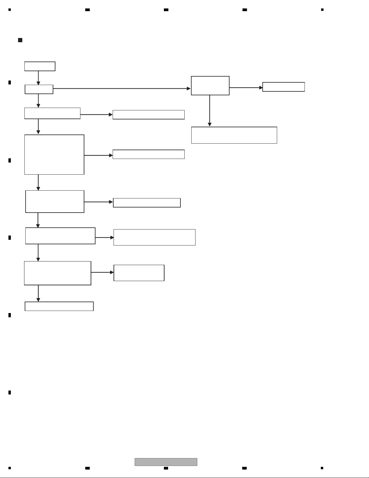
1
This is just for general reference and does not including every single case.
No Power
Error
Indications ?
Stand by
Replace D MAIN ASSY
No
Yes
Yes
Refer to
"5.4 ERROR INDICATIONS"
Other
trouble.
FUSE FU4 OPEN ?
No
Yes
Replace PRIMARY ASSY
Check PRIMARY
ASSY JP51-1,2,3Pin
or D MAIN ASSY
CN9501-1,2,3Pin
+5.6V
No
Replace PRIMARY ASSY
Yes
Check D MAIN
ASSY CN601-1,2Pin
+5.6V
No
Replace D MAIN ASSY
Yes
Check DISPLAY ASSY
CP3001-38,39Pin +5.6V
No
Replace FFC D MAIN ASSY
to DISPLAY ASSY
Yes
Check DISPLAY ASSY
C3021 +3.3V
and X3001 Oscillating
No
Replace
DISPLAY ASSY
Yes
No Power
No
2 3 4
5. DIAGNO SIS
5.1 DIAGNOSIS FLOWCHART
A
B
C
D
E
F
28
1
VSX-53
2 3 4
Page 29

5
This is just for general reference and does not including every single case.
No DISPLAY
Dimmer ?
No
"FL OFF" LED
Light on ?
Yes
No
JP3005 1-2pin
4.3Vac
Yes
No
Replace Transformer
V3301 1-62pin
4.3Vac
No
V3301Damage?
Yes
No
Yes
Replace V3301
Replace DISPLAY ASSY
JP3005 3pin -30V
JP3005 4pin +5V
Replace REGULATOR ASSY
No
Yes
No DISPLAY
6 7 8
A
B
C
D
E
F
VSX-53
5
6 7 8
29
Page 30

1
This is just for general reference and does not including every single case.
No Sound
Head Phone
Speaker Front ch
Speaker
Except Front ch
Pre OUT Front ch
Replace MIC HP ASSY
Yes
No
No
Analog in
Pure Direct
→
Pre out sound
Yes
A-DAC BRIDGE ASSY
CN3794,CN3793 21,23 pin
Signal
Replace AUDIO ASSY
Replace
POWER AMP ASSY and
PRESTAGE ASSY
No
No
No
Yes
No
No
Yes
Yes
Replace DAC LOW ASSY
Yes
Zone2 Audio No
output
Analog in
→
output
Yes
No
Digital in
→
output
No
Yes
No
Check MIC HP ASSY
CN3473 1 or 3 pin (HP
OUTPUT SIGNAL)
Yes
Check CONNECTORS
MIC HP ASSY CN3473 - AUDIO
ASSY JH2505
No Problem /
No Damage
No
Replace AUDIO ASSY
Analog Input
Digital Input
INPUT ?
Auto Surround
Pre OUT Front ch
A-DAC BRIDGE ASSY
CN3794,CN3793 25,27 pin Signal
D-DAC BRIDGE ASSY
CN3781 20,23,24,27 pin
Clock,Data
D-DAC BRIDGE ASSY
CN3781 3,9,10,12pin
Clock,Data
Replace D MAIN ASSY
D DAC BRIDGE ASSY
CN3781 5pin Clock
Replace DAC LOW ASSY
Yes
Pre OUT Front ch
Signal
No
Yes
AUDIO ASSY
CN3052 10,14pin Signal
Yes
No
Replace AUDIO ASSY
Pre OUT
Except Front ch
A-DAC BRIDGE ASSY
CN3794,CN3793
5,7,9,11,13,15,17pin Signal
Yes
No
Analog Input
Digital Input
A-DAC BRIDGE ASSY
CN3794,CN3793 25,27 pin Signal
No
D-DAC BRIDGE ASSY
CN3781 20,23,24,28,29,30 pin
Clock,Data
Yes
Replace DAC LOW ASSY
Yes
No
Pre OUT
Except Front ch
Signal
No
Yes
AUDIO ASSY
CN3052 6,8,12,16,18pin
Signal
Replace
POWER AMP ASSY and
PRESTAGE ASSY
Yes
No
A-DAC BRIDGE ASSY
CN3794,CN3793 1,3 pin Signal
D-DAC BRIDGE ASSY
CN3781 14,15,16,18pin
Clock,Data
Y
No
Replace AUDIO ASSY
Replace AUDIO ASSY
Replace AUDIO ASSY
INPUT ?
Replace AUDIO ASSY
Replace AUDIO ASSY
Replace D MAIN ASSY
No Sound
2 3 4
A
B
C
D
E
F
30
VSX-53
1
2 3 4
Page 31

BT in →(Other Analog OK)
Tuner →(Other Analog OK)
Sirius in →(Other Analog OK)
USB in →(Other Digital OK)
Front HDMI in
→
Zone2 Audio No
output
Analog in
→
output
Yes
No
Digital in
→
output
No
Yes
No
Rec out no output
Same input Function ?
It is specification.
Yes
No
Rear HDMI in
→
output
Replace FRONT HDMI USB
ASSY or HDMI Cable
from FRONT HDMI USB ASSY
Yes
No
Check D MAIN
ASSY CN1501
2,3 pin Digital Signal
Replace FRONT HDMI USB
ASSY
No
A-DAC BRIDGE ASSY
CN3794,CN3793 1,3 pin Signal
D-DAC BRIDGE ASSY
CN3781 14,15,16,18pin
Clock,Data
Yes
No
Zone3 Audio No
output
AUDIO ASSY CN3902
7,9pin Signal
AUDIO ASSY CN3902
8pin +5V
Yes
No
Yes
Replace TUNER MODULE
No
A-DAC BRIDGE ASSY
CN3791,CN3792
12,14pin Signal
Yes
No
Replace DAC LOW ASSY
D-DAC BRIDGE ASSY
CN3785 1,3pin Signal
Yes
No
FRONT HDMI USB ASSY
JP8101 1pin +13V
Yes
No
USB RECT ASSY
FU10 Open
Replace FU10
Yes
No
Replace USB RECT ASSY
Yes
No
H.M.G. in
→
(Other Digital OK)
Replace AUDIO ASSY
Replace D MAIN ASSY
Replace DAC LOW ASSY
Replace AUDIO ASSY
Replace AUDIO ASSY
Replace AUDIO ASSY
Replace AUDIO ASSY
Replace D MAIN ASSY
Replace D MAIN ASSY
Replace D MAIN ASSY
Replace D MAIN ASSY
Replace AUDIO ASSY
5
6 7 8
A
B
C
D
E
5
VSX-53
6 7 8
F
31
Page 32

1
This is just for general reference and does not including every single case.
No Picure
Composite in
→
Composite out or
zone2 Video out
Component in
→
Component out ?
HDMI in → HDMI out ?
Composite
(Component) in
→
HDMI out ?
GUI ?
iPod Video in
→
Composite out ?
R
C
No
No
No
Replace D MAIN ASSY
No
No
No
Analog Video IN ? DVC Setting ?
ON
OFF
DVC → OFF
There is problem
when DVC is OFF
No problem
when DVC is OFF
Ch
CO
CN
R
C
DVC → ON, Check
COMPONENT ASSY
CN8301 Video Signals
IN:OK,OUT:NG
Other Results
Replace
COMPONENT ASSY
No
Is there any problem
analog video IN ?
(When DVC=ON)
No
Yes
Replace D MAIN ASSY
No Picture
A
2 3 4
B
C
D
E
F
32
1
2 3 4
VSX-53
Page 33

5
Rear Composite in →
Composite out
Yes
No
No
No
No
Replace MIC HP
ASSY
Check MIC HP ASSY
→
MIC CONNECT ASSY
→
COMPONENT ASSY
Conection
No Problem
Problem
Replace Problem
Point
Check
COMPONENT ASSY
CN8303 Video Signals
IN:OK,OUT:NG
Other Results
Replace
COMPONENT ASSY
Replace
COMPOSITE ASSY
6 7 8
A
B
C
D
E
F
VSX-53
5
6 7 8
33
Page 34

1
This is just for general reference and does not including every single case.
12V Trig
RS-232C
RF Remote
IR/SR
Network
Connect or
iControlAV
No
Replace D MAIN ASSY
12VTrig
IR/SR
RS-232C
Replace POWER AMP ASSY
No
Remote Control
Replace DISPLAY ASSY
No
Yes
Replace COMPONENT ASSY
No
Replace POWER AMP ASSY
RF Remote
No
POWER AMP ASSY
JA5815 1pin +5V
Yes
Replace POWER AMP ASSY
No
Is 232C OK?
NG
OK
It's problem of the RF
Receiver Box or RF
Remote Controler
No
Network
A
2 3 4
B
C
D
E
F
34
1
VSX-53
2 3 4
Page 35

5
GAMP
R5747
C5743
CN602
-15
CN601
-26
[1] Protection Circuit Process List
DC Detection Circuit
Item Purpose Detection Method Process Warning Indication Remarks
DC
detection
To detect amplifier damage
(defect status)
A process to protect speakers
(for protection of connected
external devices)
Detects when the XDCERR port
becomes "L".
(Pin 80 of IC3001)
Turns muting on and
speaker relay off, then
turns off the power after 3
seconds. Then flashes
MCACC indicator.
Flashing "AMP ERR" for
3 seconds.
Once detected and turned
the power off, the power
cannot be turned on again
(*). If the XDCERR port
becomes "L" within 3
seconds, the unit returns
to normal condition
automatically.
AMP
overload
To detect overloading
(abnormal status)
With low-load driving or a
short circuit of the speaker
terminals (for protection of the
amplifier)
Detects when the XOLERR port
becomes "L" (checks by interrupt).
(Pin 71 of IC3001)
Turns muting on and
speaker relay off, and
immediately turns off the
power. Then flashes
iPod/iPhone indicator.
None
(*) To restore the previous staus, follow the procedure
described in “How to Enter Release Mode” (P.40)
then turn the unit back on.
R5744
R5746
R5742
Q5742
GAMP
GNDU
Q5741
Q5744
Q5743
Q5301
Q5302
R5341
OUTPUT
DC DETECTOR
R ch
C ch
SR ch
SBR ch
SL ch SBL ch
+VL
V+5UST
V+5_ST
Normal: High (5V)
DC det: Low (0V)
+DC detection: Q5741/Q5743 base is "H".
–> Collector of Q5741, Q5742, Q5743 and Q5744 are "L".
-DC detection: Q5742/Q5744 emitter is minus to the base.
–> Collector of Q5741, Q5742, Q5743 and Q5744 are "L".
-VL
R5342
R5441
R5442
R5541
R5542
R5325
R5327
R5326
R5741
R5641
R5642
C5741
R3057
C3015
D3005
D3004
UCOM
IC3001
80
CN5805
-16
L ch
R5041
R5042
R5141
R5142
R5241
R5242
CN3001
-14
POWER AMP ASSY DISPLAY ASSY
J
H
DIGITAL MAIN
ASSY
E
6 7 8
5.2 CIRCUIT DESCRIPTION
A
B
C
D
E
5
VSX-53
6 7 8
F
35
Page 36

1
OL (Over Load) Detection Circuit
Q5731
GAMP
GNDU
GNDU
Q5041
D5043
D5143
D5243
Q5001
Q5002
R5043
R5732
R5044
OUTPUT
OL DETECTOR
L ch
R ch
C ch
SL ch
SBL ch
SR ch
SBR ch
+VL
V+5_ST
V+5_UST
Normal: High (5V)
OL det: Low (0V)
-VL
R5025
R5027
R5026
R5045
R5047
R5733
R5736 R5735
D5041D5042
R5046
C5041
NP
C5731
C3014
D3003D3003
UCOM
IC3001
71
Normal: Low (0V)
OL det: 0.6V
CN5805
-10
CN3001
-31
POWER AMP ASSY
DISPLAY ASSY
J
D5443
D5543
D5343
D5143
DIGITAL MAIN
ASSY
E
R3049
H
CN603-2CN601
-9
A
2 3 4
B
C
D
E
F
36
VSX-53
1
2 3 4
Page 37

5
[2] Protection Circuit Process List (XPROTECT)
XPROTECT Circuit
Item Purpose Detection Method Process Warning Indication Remarks
XPROTECT
AMP power supply circuit and
Transformer short circuit
detect. (defect status)
Observe CN5701 pin3 or pin5
voltage, VL+ and VL-.
Detects when the XPROTECT
port becomes "L".
(Pin 83 of IC3001)
Turns muting on and
speaker relay off, and
immediately turns off the
power. Then flashes
MCACC indicator.
None
Once detected and turned
the power off, the power
cannot be turned on again.
(*)
(*) To restore the previous status, follow the procedure
described in “How to Enter Release Mode” (P.40)
then turn the unit back on.
POWER AMP ASSY
H
DISPLAY ASSY
J
UCOM
IC3001
83
R5723
47k
R5725
47k
R5726
47k
R5727
220k
R5728
220k
D5721
1SS352
D5722
1SS352
10u/63
C5723
TS
GAMP
D5782
UDZS7R5(B)
LTC124EUB
Q5781
LTC124EUB
Q5782
LTA124EUB
Q5783
LTA124EUB
Q5784
D5783
1SS352
D5784
1SS352
D5781
UDZS5R1(B)
C5781
0.01u/50
GNDU
R5781
1k
V+5_UST
Short circuit detect:
AMP power supply circuit (VL)
Short circuit detect:
Transformer
R5782
10k
R5783
10k
VL+
VL-
GNDU
V+5_UST
R5784
47k
LTC124EUB
Q5785
GNDU
R5785
100k
R5724
47k
C5782
1u/10
CN5701
-5
CN5805
-15
CN3001
-13
CN5701
-3
GNDU
R3060
1M
C3016
0.047u/50
DIGITAL MAIN ASSY
E
CN602
-17
CN601
-27
V+5_UST
V+5_ST
R5786
10k
D3005
D3004
6 7 8
A
B
C
D
5
VSX-53
6 7 8
E
F
37
Page 38

1
XVDDERR Circuit
GNDU
C3013
UCOM
IC3001
70
DISPLAY ASSY
J
R3048
FRONT HDMI USB ASSY
G
[3] Protection Circuit Process List (XVDDERR)
Item Purpose Detection Method Status of Equipment Warning Indication Remarks
USB
power
failure
detection
Detection of failure
in regulator circuit
for external supply
Detected when USB
voltage reaches 7V or
higher, or 4.1V or lower
and XVDDERR port is
set to "L"
Shuts down Blinks iPod
Restoration
possible with
Power ON
CN3003
-5
CN8004
-5
V+5_USB_DC
Q8102
LSC4081UB(QRS)
A
2 3 4
B
C
D
E
F
38
1
2 3 4
VSX-53
Page 39

5
FL Display LED flashes Status Timing (sec.) Description Remarks
AMP ERR
ADVANCED
MCACC
LED
When the AMP DC
is detected.
FL flashes 3 times.
LED flashes after
the power off.
NA
“AMP overload”
detection.
iPod iPhone
iPad LED
LED flashes after
the power off.
Abnormality detection
in the power supply
VL circuit.
Overheat detection
over 120 °
C
When the unit recovers the normal state within 3 seconds, FL
stops flashing and all zone off, and then the unit restarts auto-
matically. When the DC detect continues for more than 3 seconds,
after a failure in the amplifier block or high DC output is detected,
the shutdown process starts, then the power will be shut off.
Then the ADVANCED MCACC LED will flash.
The power cannot be turned on again.
If you wish to turn on the unit after a shutdown activated by DC
detection, enter DC detection cancellation mode,
by proceeding with the steps described in "How to enter release
mode" next page.
Upon detection of overcurrent at the amp output stage,
the unit power off immediately,
and the iPod iPhone iPad LED starts flashing.
The previous stage will be restored when the unit
is turned back on.
[4] Error Indications When an Abnormality in The Amplifier System Is Detected
[Purpose]
Errors upon detection of abnormalities in the amp system are indicated.
[Error Indications]
(1)
(2)
(3)NA
ADVANCED
MCACC
LED
iPod iPhone
iPad LED
When an abnormality is
detected in the output
voltage of the power
supply circuit.
LED flashes after
the power off.
(4) NA
When an abnormality is
detected in the output
voltage of the Digital
power supply circuit.
LED flashes after
the power off.
FL flashes 3 seconds.
LED flashes after
the power off.
(5) AMP OVERHEAT
FL OFF LED
When an abnormality of
temperature is detected
at the Amp output stage.
(6) Over Current NA
When the overload USB
device (over 500 mA) is
connected.
If abnormality voltage is detected in the power supply
VL circuit, the unit power off immediately, and the
ADVANCED MCACC LED starts flashing.
The power cannot be turned on again. If you wish to
turn on the unit after the shutdown activated by
XPROTECT, enter DC detection cancellation mode by
proceeding with the steps described in "How to enter
release mode" next page.
If abnormality voltage is detected in the Digital power supply
circuit, the unit power off immediately, and the iPod iPhone iPad
LED starts flashing. To restore the previous status, turn the unit
back on.
When the unit recovers the normal state within 3 seconds,
FL stops flashing.
When the overheat state continues for more than 3 seconds,
the power is shut off and FL OFF starts flashing.
To restore the previous status 1 minuite or more after a
shutdown, just turn the unit bac
k on.
The connected U
SB device is overload.
(7)
HDCP ERROR
NA
When an HDCP ERROR
is detected.
Flashes 5 seconds
Warning indication
for HDMI Simplay
6 7 8
A
B
C
D
E
F
VSX-53
5
6 7 8
39
Page 40

1
FL Display LED flashes Status Timing (sec.) Description Remarks
The Icon “OVER”
lights
(8) 12V TRG ERR NA
When the 12V trigger
circuit is short-circuited.
Flashes
During Standby mode, simultaneously press and hold the "TUNE [
↓
]" and "MULTI-ZONE ON/OFF" keys
for 5 seconds.
[How to Enter Release Mode]
The 12V trigger circuit is short-circuited, and a
overcurrent is generated.
(9) NANA
WLAN POW ERR
When the ANALOG INPUT
OVER is detected.
Icon lights 1 second
While the Icon lights 1 second, when the ANALOG INPUT
OVER is detected again, the Icon continues to light 1 second
more from that time.
While the Icon lights 1 second, when there is no ANALOG
INPUT OVER detection , the Icon stops lighting and returns
to normal display.
(10) NA
When BT Adapter is not
connected.
Lights
While the ADAPTER PORT function is selected, the BT Adapter
is not connected.
NO ADAPTER
(11) NA
Non-BT Adapter is
connected.
Lights
While the ADAPTER PORT function is selected, the non-BT
Adapter is connected.
NOT AVAILABLE
(12) NA
No wireless connection
between BT source and
AVR
Lights
While the ADAPTER PORT function is selected, there is no
wireless connection between BT source equipment and AVR.
WAITING DEVICE
(13)
(14)
NA
NA
When overcurrent is
detected in the Adapter port.
When power abnormality of
wireless LAN converter is
detected.
Lights
Flashes
While the ADAPTER PORT function is selected, overcurrent is
detected in the Adapter port, and Bluetooth function is not
available.
Over-current status is generated at the power terminal of
wireless LAN converter.
ADP OVERLOAD
A
2 3 4
B
C
D
E
F
40
1
2 3 4
VSX-53
Page 41

5
Key operation FL display
Display number of times
DC is detected.
Display number of times
OVERLOAD is detected.
Display number of times
COMBINATION is detected.
(Detects DC and OVERLOAD
simultaneously)
Display number of times
Power abnormality is
detected.
Display number of times
AMP overheat is
detected.
[↓]
[↑]
[↓]
[↑]
[↓]
[↑]
[↓]
[↑]
[↓]
[↑]
Display number of times
Digital Power abnormality is
detected.
Resetting the number of
times error is detected.
[↓]
[↑]
[↓]
[↑]
OL
:
DC
:
:
:
COM
XPRT
:
S TMP
RES ET
RES ET
RES ET
:
DERR
The numbers of detections for various protection processes are displayed.
[↓] : TUNE key
[↑] : TUNE key
[←] : PRESET key
[→] : PRESET key
During Standby mode, simultaneously press and hold “MULTI-ZONE ON/OFF” and “ENTER” keys for 5 seconds to enter
this mode.
Turning off the power or pressing the Return key returns to the normal mode.
Turn off the power to this unit by setting the main volume level to “---dB” and Multi-zone to “OFF”.
Display number of times
FAN STOP is detected.
This function does not work
on this model.
[↓]
[↑]
:
FAN
RES ET
HOLD
CLEAR?
Resetting the number of times error is detected
Key operation FL display
↓
Continued
[ENTER]
[←][→]
[1] Detected protection history
[Purpose]
[How to enter/exit]
[Basic operations]
Front Panel Key
6 7 8
6. SERVICE MODE
6.1 TEST MODE
A
B
C
D
E
5
VSX-53
6 7 8
F
41
Page 42

1
Key operation FL display
Display CEC(TEST) state.
Display FAN(TEST) state.
USB Backup state
[↓]
[↑]
[↓]
[↑]
[↓]
[↑]
U S B BAK
CEC
OFF
FAN
CEC
ON
OFF
HOLD
Display
Model Name/Destination
state.
[↓]
[↑]
V S X-53 /UXJCB
U S B BAK
PLEAS E WAIT
COMPLETE
S AVE?
U S B BAK LOAD?
Display CEC(TEST) state.
Key operation FL display
↓
Change cyclically
[←][→]
Saving and Loading of USB backup state.
(A/V Receiver
→ USB)
(USB → A/V Receiver)
Key operation FL display
↓
Change cyclically
5 sec
SAVE or LOAD
is completed.
[←][→]
[←][→]
Key operation FL display
↓
Power OFF
(All zone OFF)
FAN
ON
Key operation FL display
↓
Change cyclically
[←][→]
Change cyclically
Display accumulated
time & RESET.
[↓]
[↑]
CL?
R S T
123 45h20m
123 45h 20m
0h 0m
HLD
Resetting the accumulated time
Key operation FL display
↓
Continued
[ENTER]
[ENTER]
[←][→]
CEC TEST : The function for making the HDMI output terminal to
output 1 kHz square wave. If the square wave is output,
the CEC line is considered to be normal.
FAN TEST : The function for making the FAN to be forced to rotate.
[Description]
This function does not work
on this model.
A
2 3 4
B
C
D
E
F
42
1
2 3 4
VSX-53
Page 43

5
100Ω 3W
or more
100Ω 3W
or more
POWER AMP ASSY
D5790
D5790
C5722
C5722
J496
J496
J552
C5721
C5721
pin 1 +
pin 4 --
Front
Preparations Before Performing Diagnosis of the POWER AMP ASSY
Before performing diagnosis of the POWER AMP ASSY, it is necessary to discharge C5721 and C5722 on the board.
(See the photo below.)
If you don't, the protectors (P5001 and P5002) on the board may be open, and DC voltage may be generated at the power
amplifier output, which will result in "AMP ERR."
[Procedures]
(1) Unplug the power cord.
(2) Discharge C5721 and C5722 by connecting either J496 or J552 to pin 1 and 4 of D5790.
Note: For discharging, use a load of 100 Ω , 3 W or more, to protect the IC protectors. Do NOT discharge instantly by
short-circuiting.
(3) Check that the voltage between the electrodes of each C5721 and C5722 is 1 V or less.
6 7 8
7. DISASSEMBLY
7.1 DISASSEMBLY
A
B
C
D
5
VSX-53
6 7 8
E
F
43
Page 44

1
Ground any one of these points.
VSX-53/UXJCB, VSX-1326-K/CUXJ, VSX-52/UXJCB only
VSX-52/UXJCB, VSX-1126-K/CUXJ, VSX-1121-K/UXJCB only
VSX-53/UXJCB, VSX-1326-K/CUXJ only
Ground any one of these points.
Ground any one
of these points.
DCB
BBZ30P080FTB BMZ30P040FTB BBT30P100FCC ABA7078
A
Ground Points
Screws for Rear Panel
Note:
The points marked below must be grounded when the rear panel is removed.
Before turning the unit ON, be sure to ground the marked points with the Under Base 55. Or, you may short-circuit the ground
points on the solder surface, using pieces of wire.
B BBB
C C C C C C
D
D
A
A A
A
A
A
AA
A A
A
AA A A A A A A A
A
AAAA
AAAA
A
A
A
A
A
A
B B B B B
A
2 3 4
B
C
D
E
F
44
1
2 3 4
VSX-53
Page 45

5
Diagnosis
Note 1 : Even if the unit shown in the photos and illustrations in this manual may differ from your product, the procedures
described here are common.
Note 2 : For performing the diagnosis shown below, the following jigs for service is required.
• 19P FFC (GGD1678)
• 20P + 14P board to board extension jig cable (GGD1759)
• 20P + 20P board to board extension jig cable (GGD1677)
• 7P + 15P board to board extension jig cable (GGD1762)
• 30P board to board extension jig cable (GGD1682) x 2
• 28P + 14P board to board extension jig cable (GGD1763)
[1] Front Section
Remove the Bonnet 55 by removing the 16 screws.
-----------------------------------------------------------------
[1-1] Exterior
(1) Remove the two screws. (BBZ30P080FTB)
(2) Remove the two screws.
(VSX-53, VSX-1326-K: ABA1193)
(VSX-52, VSX-1126-K, VSX-1121-K:
BBZ30P080FTB)
(3) Disconnect the four connectors.
(4) Remove the three screws. (BBZ30P080FCC)
(5) Release the cables from the two
Binders.
(6) Disconnect the connector.
(7) Disconnect the connector.
(8) Remove the three screws. (BBZ30P080FCC)
2
2
1 1
5
8 8 8
6
5
CN4052
CN3473 CN3471
CN8101 JA8003
REGULATOR ASSY
MIC HP ASSY
FRONT HDMI USB ASSY
7
USB RECT ASSY
CN3652
3
4
4
3
6 7 8
A
B
C
D
E
F
VSX-53
5
6 7 8
45
Page 46

1
(9) Release the cables, as required.
(10) Disconnect the 39P FFC (ADD7751) from
the DIGITAL MAIN ASSY.
(11) Unhook the two hooks.
(12) Remove the Front Section.
(13) Release the three cables, as required.
(14) Remove the two screws. (BBZ30P080FCC)
(15) Remove the MIC CONNECT ASSY.
(16) Release the jumper wires from the Binder.
(17) Cut the Binder.
Note1: When assembled, the wires should be
styled as shown in the photo below.
Note2: Please connect a wire to the resistor
(R4022) in REGULATOR ASSY with
200-gf without touching.
9
x 4
9
DIGITAL MAIN ASSY
CN601
BIND L BACK ASSY
39P FFC
BIND L FRONT ASSY
Front Section
11 11
12
10
14
14
15
13
13
13
USB RECT ASSY
MIC CONNECT ASSY
16
17
BIND R FRONT ASSY
Jumper wire of
the AUDIO ASSY
Binder
JP2505
Front
Front
A
2 3 4
B
C
D
E
F
46
VSX-53
1
2 3 4
Page 47

5
[1-2] Diagnosis
Connect the seven connectors and arrange the unit as shown in the photo.
DIGITAL MAIN ASSY
CN601
DISPLAY ASSY
CN4052
CN3473 CN3471
CN8101
JA8003
REGULATOR ASSY
MIC HP ASSY
FRONT HDMI USB ASSY
USB RECT ASSY
CN3652
MIC CONNECT ASSY
POWER SW ASSY
ENCODER ASSY
VOL ASSY
6 7 8
A
B
C
D
5
VSX-53
6 7 8
E
F
47
Page 48

1
5
3
1
2
4
BIND R FRONT ASSY
BIND R BACK ASSY
PRESTAGE ASSY
Power Transformer
Front
DIGITAL MAIN ASSY
CN3052
CN6603
[2] POWER AMP ASSY, AUDIO ASSY
When you perform diagnosis on the side-B of
AUDIO ASSY, please refer to the last part of
Step, “[4-2] Diagnosis”.
(1) Remove the Bonnet 55 by removing the 16
screws.
(2) Discharge C5721 and C5722.
(Refer to the “discharge procedures.”)
-----------------------------------------------------------------
[2-1] Exterior
(1) Release the cables, as required.
(2) Cut the two Binders.
Note1: When assembled, the wires should be
styled as shown in the photo below.
Note2: Please connect a wire to the resistor
(R4022) in REGULATOR ASSY with
200-gf without touching.
(3) Release the cable, as required.
(4) Cut the Binder.
(5) 19P FFC (ADD7730) to 19P FFC (GGD1678)
to replace.
(6) Release the cables, as required.
(7) Cut the Binder.
(8) Disconnect the two connectors.
PRESTAGE ASSY
AUDIO ASSY
19P FFC
6
6
8
8
x 4
6
DIGITAL MAIN ASSY
CN601
JA905
BIND L BACK ASSY
7
Binder
39P FFC
HDMI CONN-Cable
BIND L FRONT ASSY
1
2
A
2 3 4
B
C
D
E
F
48
1
VSX-53
2 3 4
Page 49

5
(9) Release the 7P FFC (ADD7750) from the
PRESTAGE ASSY.
(10) Remove the Nylon Rivet.
(11) Remove the screw. (BBZ30P080FCC)
(12) Disconnect the two connectors.
(13) Remove the screw. (BBZ30P080FCC)
(14) Remove the Right Angle 55.
(15) Connect the 39P FFC. (ADD7751)
Note: The 39P FFC (ADD7751) is passed under
the 5P Housing ASSY.
DIGITAL MAIN ASSY
Front
Front
PRESTAGE ASSY
9
Right Angle 55
7P FFC
39P FFC
DIGITAL MAIN ASSY
DIGITAL MAIN ASSY
CONNECT ASSY
x 2
CN601
13
11
14
15
5P Housing ASSY
Right Angle 55
Right Angle 55
12
10
6 7 8
A
B
C
D
E
F
VSX-53
5
6 7 8
49
Page 50

1
(16) Remove the six Cushion Circle 14B.
(17) Remove the six screws. (BBT30P100FCC)
(18) Remove the eleven screws.
(BBZ30P080FTB)
(19) Remove the AC inlet.
[2-2] Diagnosis
(1) Arrange the unit as shown in the photo.
(2) Connect the Rear Panel to the Under Base
55 Ground.
(3) Insert the Insulation Sheet.
(4) Connect the two board to board extension
jig cables.
(DIGITAL MAIN CN602 <-> CONNECT CN3362)
(DIGITAL MAIN CN603 <-> CONNECT CN3361)
x 6
16
x 6
17
19
AC inlet
18
18
18
18
18
2
3
4
POWER AMP ASSY
AUDIO ASSY
Rear Panel
Under Base 55
1
Insulation Sheet
CN3361
CN3362
CN602
CN603
CONNECT ASSY
DIGITAL MAIN ASSY
20P + 14P board to board
extension jig cable (GGD1759)
A
B
2 3 4
C
D
E
F
50
1
VSX-53
2 3 4
Page 51

5
[2-3] Remove the POWER AMP ASSY
(1) Disconnect the two board to board extension
jig cables. (GGD1759)
(Refer to the step (4) of “[2-2] Diagnosis”)
(2) Cut the two Binders.
(3) Disconnect the two connectors.
(4) Disconnect the 19P FFC.
(Jig cables : GGD1678)
(5) Disconnect the five connectors from the
DIGITAL MAIN ASSY.
(6) Arrange the unit as shown in the photo.
DIGITAL MAIN ASSY
POWER AMP ASSY
PRESTAGE ASSY
CONNECT ASSY
AUDIO ASSY
DIGITAL MAIN ASSY
CN601
CN604
CN605
CN606
CN9501
CN3052
CN6603
39P FFC
Front
BIND L BACK ASSY
BIND L FRONT ASSY
2
2
3
19P FFC
x 2
4
5
5
5
5
5
4
6 7 8
A
B
C
D
5
VSX-53
6 7 8
E
F
51
Page 52

1
(7) Remove the two screws. (BBZ30P080FCC)
(8) Release the cables from the Wire Saddle.
(9) Disconnect the connector from the POWER
AMP ASSY.
(10) Remove the two Nylon Rivets.
(11) Remove the two screws. (BBZ30P080FCC)
(12) Remove the POWER AMP ASSY from the
three Locking Card Spacer 18, using Pliers.
(13) Remove the POWER AMP Unit.
Locking Card Spacer 18
12
CN5701
POWER AMP ASSY
POWER AMP Unit
POWER AMP ASSY
7
7
12
12
13
8
9
Power Transformer
Wire Saddle
Pliers
Front
11
10
10
A
B
C
2 3 4
D
E
F
52
1
2 3 4
VSX-53
Page 53

5
(14) Remove the Nylon Rivet.
(15) Disconnect the seven connectors and then
remove the PRESTAGE ASSY.
(16) Remove the two Nylon Rivets.
(17) Remove the 14 screws. (ABA7085)
(18) Remove the POWER AMP ASSY.
[2-4] Assembling of the POWER AMP ASSY
(1) Attach the POWER AMP ASSY to the Heat
Sink, using the 14 screws (ABA7085) and
two Nylon Rivets.
(Refer to the steps (17) and (16) of “[2-3]
Remove the POWER AMP ASSY”)
Note: Apply even coatings of silicon grease
(GEM1057) on the Heat Sink side of the
transistors.
(2) Connect the seven connectors and then
attach the PRESTAGE ASSY, using the
Nylon Rivet.
(Refer to the steps (15) and (14) of “[2-3]
Remove the POWER AMP ASSY”)
(3) Attach the POWER AMP Unit to the Under
Base 55.
(Refer to the steps (12) to (7) of “[2-3]
Remove the POWER AMP ASSY”)
14
15
POWER AMP ASSY
POWER AMP ASSY
PRESTAGE ASSY
16
17
18
16
Heat Sink
x 14
6 7 8
A
B
C
5
6 7 8
VSX-53
D
E
F
53
Page 54

1
(4) Allocate the Rear Section as shown in the
photo.
(5) Attach the nine screws. (BBZ30P080FTB)
(6) Attach the six screws. (BBT30P100FCC)
(7) Attach the AC inlet, using the two screws.
(BBZ30P080FTB)
(8) Attach the Right Angle 55, using the two
screws (BBZ30P080FCC) and Nylon Rivet.
Note: The 3P Housing ASSY is passed through
the hole of the Right Angle 55.
The jumper wires is passed over the Right
Angle 55.
Rear Section
x 6
AC inlet
15
5
5
5
5
5
6
7
3P Housing ASSY
Jumper wires
Right Angle 55
Hole
Front
8
8
8
A
B
2 3 4
C
D
E
F
54
1
2 3 4
VSX-53
Page 55

5
(9) Connect the two connectors.
(10) Connect the two connectors.
Note: The jumper wires is passed over the Right
Angle 55.
(11) Fix the 7P FFC (ADD7750) to the
PRESTAGE ASSY.
(12) Connect the connector.
(13) Fix the 39P FFC (ADD7751).
(14) Fix the 5P Housing ASSY.
(15) Connect the connector.
(16) Fix the some cables as shown in the photo.
(17) Fix the some cables as shown in the photo.
(18) Connect connector and fix the some cables
as required.
(Refer to steps (5) to (1) of “ [2-1] Exterior”)
Front
Front
DIGITAL MAIN ASSY
CONNECT ASSY
10
11
12
13
14
15
Jumper wires
Right Angle 55
7P FFC
39P FFC
DIGITAL MAIN ASSY
CN601
x 4
JA905
BIND L BACK ASSY
BIND L BACK ASSY
BIND L FRONT ASSY
BIND L FRONT ASSY
HDMI CONN-Cable
16
17
x 3
PRESTAGE ASSY
5P Housing ASSY
9
6 7 8
A
B
C
D
E
F
5
VSX-53
6 7 8
55
Page 56

1
(19) Connect the three connectors.
Note: The junper wire of the POSI 2 ASSY is
twined round the junper wire of the POSI 3
ASSY three times.
(20) Attach the six Cushion Circle 14B.
(Refer to step (16) of “ [2-1] Exterior”)
[3] DAC LOW ASSY
(1) Remove the Bonnet 55 by removing the 16
screws.
(2) Discharge C5721 and C5722.
(Refer to the “discharge procedures.”)
-----------------------------------------------------------------
[3-1] Exterior
(1) Remove the D-DAC BRIDGE ASSY.
(2) Remove the A-DAC BRIDGE ASSY.
(3) Remove the screw. (BMZ30P040FTB)
(4) Remove the five screws. (BBZ30P080FTB)
Front
DIGITAL MAIN ASSY
CN606
CN605 CN604
POSI 3 ASSY POSI 1 ASSYPOSI 2 ASSY
Front
x 5
4
3
DIGITAL MAIN ASSY
Screwdriver
A-DAC BRIDGE ASSY
D-DAC BRIDGE ASSY
1
2
A
2 3 4
B
C
D
E
F
56
1
VSX-53
2 3 4
Page 57

DIGITAL MAIN ASSY
AUDIO ASSY
(5) Remove the DAC LOW ASSY.
[3-2] Diagnosis
(1) Connect the two board to board extension jig
cables.
(DAC LOW CN2102 <-> DIGITAL MAIN CN9003)
(DAC LOW CN2101 <-> DIGITAL MAIN CN9002)
(2) Connect the two board to board extension jig
cables.
(DAC LOW CN2103 <-> AUDIO CN2502)
(DAC LOW CN2104 <-> AUDIO CN3001)
DAC LOW ASSY
Front
Front
DAC LOW ASSY
CN2102
CN2101
CN2103
CN2104
1
2
30P board to board extension
jig cable (GGD1682) x 2
28P + 14P board to board
extension jig cable (GGD1763)
CN2502
CN9003
CN9002
CN3001
5
6 7 8
A
B
C
D
E
VSX-53
5
6 7 8
F
57
Page 58

1
(3) Insert the Insulation Sheet.
(4) Connect the DAC LOW ASSY to the Rear
Panel ground.
(Refer to the “Ground points.”)
[4] DIGITAL MAIN ASSY
(1) Remove the Bonnet 55 by removing the 16
screws.
(2) Discharge C5721 and C5722.
(Refer to the “discharge procedures.”)
-----------------------------------------------------------------
[4-1] Exterior
(1) Release the cables, as required.
(2) Cut the Binder.
(3) Disconnect the two connectors.
(4) Disconnect the connector.
3
4
Rear Panel
Insulation Sheet
DAC LOW ASSY
CN3653
MIC CONNECT ASSY
3P Housing ASSY
Front
1
1
3
3
x 4
1
DIGITAL MAIN ASSY
CN601
JA905
BIND L BACK ASSY
BIND L FRONT ASSY
2
39P FFC
HDMI CONN-Cable
A
2 3 4
B
C
D
E
F
58
1
2 3 4
VSX-53
Page 59

5
(5) Connect the 39P FFC (ADD7751).
Note: The 39P FFC (ADD7751) is passed over
the HDMI CONN-Cable.
The 39P FFC (ADD7751) is passed under
the 5P Housing ASSY.
(6) Disconnect the two connectors.
(7) Remove the screw. (BBZ30P080FCC)
(8) Remove the two Hex head Screws.
(ABA7078)
(9) Remove the some screws.
(BMZ30P040FTB)
(VSX-53, VSX-1326-K: x 8)
(VSX-52, VSX-1126-K, VSX-1121-K: x 7)
(10) Remove the seven screws.
(BBZ30P080FTB)
(11) Remove the D-DAC BRIDGE ASSY.
(12) Remove the A-DAC BRIDGE ASSY.
(13) Remove the D-AUDIO BRIDGE ASSY.
Front
39P FFC
DIGITAL MAIN ASSY
CN601
5P Housing ASSY
CONNECT ASSY
HDMI CONN-Cable
x 2
6
5
7
8
9
x 6
D-AUDIO BRIDGE ASSY
DIGITAL MAIN ASSY
Screwdriver
D-DAC BRIDGE ASSY
A-DAC BRIDGE ASSY
11
12
10
10
13
6 7 8
A
B
C
D
E
F
VSX-53
5
6 7 8
59
Page 60

1
(14) Arrange the DIGITAL MAIN ASSY (with the
COMPONENT ASSY and the COMPOSITE
ASSY) as shown in the photo.
(15) Insert the Insulation Sheet.
(16) Disconnect the connector and then remove
the COMPOSITE ASSY.
[4-2] Diagnosis
(1) Attach the COMPOSITE ASSY, using the
four screws. (BBZ30P080FTB)
(2) Connect the two board to board extension jig
cables.
(DIGITAL MAIN CN602 <-> CONNECT CN3362)
(DIGITAL MAIN CN603 <-> CONNECT CN3361)
(3) Connect the two board to board extension jig
cables.
(COMPONENT CN8303 <-> CONPOSITE CN3601)
Front
x 4
3
2
CN3361
CN3362
CN602
CN603
CN3601
CN8303
CONNECT ASSY
DIGITAL MAIN ASSY
COMPOSITE ASSY
COMPONENT ASSY
20P + 14P board to board
extension jig cable (GGD1759)
20P + 20P board to board
extension jig cable (GGD1677)
COMPONENT ASSY
COMPOSITE ASSY
DIGITAL MAIN ASSY
Insulation Sheet
14
15
16
A
2 3 4
B
C
D
E
F
60
VSX-53
1
2 3 4
Page 61

5
(4) Remove the DAC LOW ASSY.
(Refer to steps (3) to (5) of
“[3-1] Exterior”)
(5) Connect the two board to board extension jig
cables.
(DIGITAL MAIN CN1503 <-> AUDIO CN3901)
(DIGITAL MAIN CN1502 <-> AUDIO CN2861)
(6) Connect the two board to board extension jig
cables.
(DAC LOW CN2103 <-> AUDIO CN2502)
(DAC LOW CN2104 <-> AUDIO CN3001)
(7) Connect the two board to board extension jig
cables.
(DAC LOW CN2102 <-> DIGITAL MAIN CN9003)
(DAC LOW CN2101 <-> DIGITAL MAIN CN9002)
(8) Insert the Insulation Sheet.
(9) Connect the DIGITAL MAIN ASSY and the
DAC LOW ASSY to the Rear Panel ground.
(Refer to the “Ground points.”)
Note1: In case of diagnosing DIGITAL MAIN ASSY
by this situation, do not connect HDMI
cable from FRONT HDMI USB ASSY to
prevent breakdown of HDMI connector.
If the HDMI connection is necessary, use
another normal HDMI cable and connect it
to DIGITAL MAIN ASSY without any stress
from HDMI cable.
Note2: By placing the DAC LOW ASSY on the
DIGITAL MAIN ASSY from the above
status, it is possible to perform diagnosis
both on the DAC LOW ASSY and the
side-B of AUDIO ASSY simultaneously.
5
6
7
9
9
CN2101
CN2102
CN9002
CN9003
CN2103
DIGITAL MAIN ASSY
DAC LOW ASSY
CN1502
CN1503
CN3001
CN2861
CN3901
7P + 15P board to board
extension jig cable (GGD1762)
28P + 14P board to board
extension jig cable (GGD1763)
30P board to board extension
jig cable (GGD1682) x 2
CN2502
AUDIO ASSY
AUDIO ASSY
CN2104
8
Insulation Sheet
Insulation Sheet
Rear Panel
DAC LOW ASSY
DIGITAL MAIN ASSY
6 7 8
A
B
C
D
E
F
VSX-53
5
6 7 8
61
Page 62

1
DISPLAY ASSY "8.3 REGION WRITING"
DIGITAL MAIN ASSY
"8.2 HOW TO SAVE AND LOAD THE SETTING USING
BACKUP FUNCTION WITH USB MEMORY"
Other assemblies No adjustment required
When any of the following assemblies is replaced
DIGITAL MAIN ASSY No adjustment required
The part listed below is difficult to replace as a discrete
component part. When the part listed in the table is
defective, replace whole Assy.
• IC101 (UPD61283F1-407LU2A)
• IC903 (
SII9233ACTU
)
• IC905 (
SII9387CTU
)
• IC1204 (88DE2750)
• IC1212(MAIN) (
H5PS5162GFR-S5C-K
)
• IC1212(SUB) (
K4T51163QI-HCE7
)
• JA1501 (
CKS5712-A )
• IC1602 (
SII9136C TU
)
• IC1603 (
SII9136C TU
)
• IC9002 (
D810K013BZKB400-K
)
• IC9203 (
LAN8700C-AEZG
)
• IC9204 (
DM860
)
• IC9205 (
AYW7346-A
)
• IC9509 (
MM1701WH
)
• IC9510 (
NJM2846DL3-33 )
Other assemblies No adjustment required
When any of the following parts is replaced
2 3 4
8. EACH SETTING AND ADJUSTMENT
8.1 ADJUSTMENT REQUIRED WHEN THE UNIT IS REPAIRED OR REPLACED
A
B
C
D
E
F
62
1
2 3 4
VSX-53
Page 63

5
[Introduction]
This model is capable of saving the set values stored in the MAIN Ucom of DIGITAL MAIN
ASSY in the USB and loadi n g th em in a new DIGITAL MAIN ASSY.
(Note that MAIN Ucom sho u l d normally operate to enable this func tion.)
When replacing DIGITAL MAIN ASSY, execute the above mentioned processes .
[Data that can be saved/cannot be saved]
The following data can not be saved. Data oth er than these can be saved.
(As the data saved by EVE NT Ucom is on t he DI SPLAY ASSY,
the data cannot be deleted unless Assy is replaced at the same time.)
[Requirements for USB memory]
USB memory to be used should meet the following requirements.
Compatibl e with USB Mass storage Class
With a file system of FAT(FAT32)
[File saving fo rm at]
Files are to be saved in the following format: Model number_backup version.extension( avr)
Example: V SX-53_BK01.avr
[How to save in the USB memory from AV amplifier]
1. Insert the usable USB memory into th e USB terminal when the main device is off.
2. Enter the SERVICE MODE and select [USB BAK
HOLD ] with keys.
(See [6.1 TEST MODE] for how to enter the SERVICE MODE.)
3. Select [USB BAK
SA VE ] with keys and press [ENTER].
4. Saving in the USB starts and the main device automatically goes off after th e nor mal completion ([ COMPLETE]
is displayed.).
5. Remove the USB and saving is finished.
*1. If the following errors occur after "SAVE" is executed, error message will be displayed and "SAVE" will be stopped
and the power will be turned off.
Ejecting of USB device
Short capacity of USB devic e
Error during writing in the USB device (Read Only or defective Sector, etc.)
*2. If the same file name exists in the USB, overwriting will b e automatically executed.
[How to write into AV amplifier from the USB memory]
1. Insert the USB with the saved file into the USB terminal when the main device is off.
2. Enter the TEST MODE and select [USB BAK
HOLD ] with keys.
(See [6.1 TEST MODE] for how to enter the TEST MODE.)
3. Select [USB BAK
LOAD ] with keys and press [ENTER].
4. Saving in the main de vi ce starts and it automatically go es off after the normal completion
([COMPLETE] is displayed.).
5. Remove the USB and loading is finished.
* If the following errors occur after "LOAD" is executed, error message will be displayed and "LOAD" will be stopped and
the power will be turned off.
No setting file
Mismatching between the setting file and the specification of the A/V RECEIVER type to be loaded back
Error due to Checksum, Signature C heck, and Size Check
Ejecting of USB device (during readi ng of the setting file)
Contents to save Destination to save
Last memory for turning ON/OFF the Main power and power supply for ZONE2 and ZONE3
Last memory for inputting the Main ZONE, ZONE2 and ZONE3
Setting for controlling HDMI
Remote c o n trol ID
Setting for RF remo te control (EXTENSION Setup)
Setting for Network Standby
Data to be save upon the operation of protection circuit
EVENT Ucom
Settings for H MG
Prese t Memory, Favorite, Recently played, etc.
BridgeCo IC
8.2
HOW TO SAVE AND LOAD THE SETTING USING BACKUP FUNCTION WITH USB MEMORY
6 7 8
A
B
C
D
E
F
VSX-53
5
6 7 8
63
Page 64

1
Precautions
Files are stored in Root of USB memory.
Files are read from Root of USB memory.
To make operations such as moving files, be sure to assign the saved file in Root
of the USB memory.
Also please be careful not to assign *.avr in multiple numbers.
The time and date of updating for saved file is fixed to "2010/01/01 0:00."
In principle, please implement Load without making of factory default settings.
To Load from factory default settings status, please take caution on the following points;
Please be sure to check the HDMI control setting for the user before performing of factory default settings.
Since the HDMI control setting of default settings is ON, turn OFF the HDMI control setting
and Load after performing of factory default settings if the checked user setting is OFF.
(If Load is executed with the setting ON, the assi
gnment i
nformation for each HDMI input
will be cleared.)
Procedures for turning OFF the HDMI control setting
HOME MENU 4.System Setup 4e.HDMI Setup Control OFF
Power On (Automatically)
Start up finished
Connect USB
Memory.
Loading finished
correctly
POWER ON
V S X-53 /UXJCB
S ET REGION
Key operation FL display
Plug in the AC cord.
(No Region information)
Function initial display
Region Writing finished
[Preparations]
1. Please copy the REGION File for the same model number and the point of destination with the object set to the route
directory of USB Memory.
Note: Copy only the REGION File to the USB memory. Never copy to other files.
[Precautions]
Please be sure to use the REGION File for the same model number and the point of destination with the object set.
If you make a mistake, it is impossible to rewrite. (Replacement of DISPLAY ASSY is required again)
[Procedures]
1. Connect an AC cord after replacing DISPLA Y
ASSY. (Power turns ON automatically)
2. [SET REGION] is displayed several seconds after
[POWER ON] is displayed on the front panel.
(Standby status for REGION File writing)
3. Automatic writing starts when USB memory
prepared by [Preparation: 1] is inserted.
(Degree of several seconds)
4. The written model number is displayed after the
normal completion of REGION File writing.
(14 characters, maximum)
5. Pull out the AC cord.
This is the function to write Region information by using an USB Memory.
Automatic start-up is conducted with POWER ON if the Region information is not written.
This work is carried out when DISPLAY ASSY is replaced.
A
B
8.3 REGION WRITING
2 3 4
C
D
E
F
64
1
2 3 4
VSX-53
Page 65

5
[Case of Abnormal Completion]
If REGION File writing did not complete normally, an error number is displayed rather than the model number.
Please perform rewriting based on the coping strategy by error numbers below.
MAIN com (EMMA), SUB com (EVENT) , DSP Flash ROM and BridgeCo IC Update
by USB Memory and the Confirmation of the Version
[Preparations]
UPDATE PANEL Mode (Version update)
1. Copy the UPDATE FILE to the root directory of the USB Memory.
Note: NEVER copy several UPDATE FILES to the root directory of the USB Memory.
Copy only the corresponding UPDATE FILE.
Enter the UPDATE PANEL mode.
Check a current version.
2. Turn off the power to this unit by setting Multi-Zone to "OFF".
3. Connect the USB Memory to the USB terminal (A type) of the front panel.
1. While holding down "TUNE↑" key on the front panel, press "STANDBY ON/OFF" key and
moves to the UPDATE PANEL mode.
2. The updating process is as follows.
[Procedures]
Workflow
Check an updated version.
Turn the power off.
(Release the UPDATE PANEL mode.)
Update it.
Update completed.
(Turn the power OFF automatically.)
Updating process
Enter the UPDATE PANEL mode again.
Checking process
FL Display Examples Reason for Display Coping Strategy
E R R O R R 0 1
6 7 8
A
Case of unsuccessful USB Read-in Try writing with ot her USB Memory
E R R O R R 0 2
E R R O R R 0 3
E R R O R R 0 4
8.4 HOW TO UPDATE FIRMWARE
Case of No File for Writing Place writing required REGION File
Case of destroyed File
Case of destination informati o n for
different mod e l is writte n
to root directory
Download REGION File again
Download REGION File for correct
model
B
C
5
6 7 8
VSX-53
D
E
F
65
Page 66

1
Update Menu
UPDATE
Update Confirmation
UPDATE ?
NO
Update Confirmation
UPDATE ?
YES
File searching
Accessing
Key operation FL display
[PRESET
→]
or
[PRESET
←]
[←]
[→]
[ENTER]
[ENTER]
UPDATE FILE searching
completed
Key operation FL display
[STANDBY ON/OFF]
[TUNE
↑] +
Version is displayed.
Version number of BridgeCo
Version number of DSP
Version number of Sub com
(EVENT)
Small version number of
Main com (EMMA)
Big version number of
Main com (EMMA)
Update Menu
Booting is completed
[TUNE↓] or [TUNE↑]
[↓]
[↑]
1-001002003 004
POWER ON
UPDATE
1-001002003 004
Front Panel Key
[↓] : TUNE key
[↑] : TUNE key
[←] : PRESET key
[→] : PRESET key
"" displayed instead of number indicates
the process while the version is obtained.
Wait for a while until the version is displayed.
A
2 3 4
B
C
D
E
F
66
1
2 3 4
VSX-53
Page 67

5
Key operation FL display
DSP UPDATE completed
Updating process
BridgeCo IC UPDATE
completed
MAIN com (EMMA) UPDATE
completed
5 Second
SUB com (EVENT) UPDATE
completed
Updating process
Update completion display
Power turns off automatically.
(All ZONE OFF)
Disconnect the USB MEMORY.
Updating process
∗ Upda ting. 20%
∗ Upda ting. 40%
∗ Upda ting. 60%
Updating process
∗ Upda ting. 8 0%
∗ Upda ting. 100%
UPDATE FILE searching
completed
[Confirmation]
Enter UPDATE PANEL mode and check that the programs have been updated.
Update time is fluctuated by contents of the update. It will take about 20 minutes at the maximum.
(Actual time is from 2 minutes to 15 minutes.)
Time required for updating varies, because only the programs that require updating will be updated.
6 7 8
A
B
C
D
VSX-53
5
6 7 8
E
F
67
Page 68

1
NOTES: - Parts marked by “NSP” are generally unavailable because they are not in our Master Spare Parts List.
-
The > mark found on some component parts indicates the importance of the safety factor of the part.
Therefore, when replacing, be sure to use parts of identical designation.
-
Screws adjacent to mark on product are used for disassembly.
-
For the applying amount of lubricants or glue, follow the instructions in this manual.
(In the case of no amount instructions, apply as you think it appropriate.)
Note ∗1: Please fix both ends of the
Protection Sheet LX with the tape.
Turn down an edge to be easy to peel off.
∗1
∗1
50
±
5mm
50
±
5mm
VSX-1121-K/UXJCB only
2 3 4
9. EXPLODED VIEWS AND PARTS LIST
A
9.1 PACKING SECTION
B
C
D
E
F
68
1
VSX-53
2 3 4
Page 69

5
(1) PACKING SECTION PARTS LIST
Mark No. Description Part No.
1 iPod Cable ADE7136
>
2 AC Power Cord ADG7111
3 FM Wire Antenna ADH7030
NSP 4 Polyethylene Bag AHG7117
5 MCACC Setup Microphone APM7010
6 7 8
Mark
No. Description Part No.
11 Remote Control Unit AXD7612
NSP 12
Dry Cell Battery
13 AM Loop Antenna XTB3004
14 Packing Pad /F AHA 7494
15 Packing Pad /R AHA7495
(AAA size IEC R03)
VEM1051
A
6 Operating instructions (En) See Contrast table (2)
7 Operating instructions (Fr) See Contrast table (2)
8Caution Sheet SP, E ARM708 3
9 Operating instructions
NSP 10 Warranty Card See Contrast table (2)
(CD-ROM)
See Contrast table (2)
16 Packing Case See Contrast table (2)
17 Packing Sheet RHC1023
18 Battery Cover AZ N8047
NSP 19 Serial Label S VRW2017
20 Protection Sheet LX See Contrast table (2)
(2) CONTR AST TABLE
VSX-53/UXJCB, VSX-1326-K/CUXJ, VSX-52/UXJCB, VSX-1126-K/CUXJ and VSX-1121-K/UXJCB are constructed
the same except for the following:
Mark No. Symbol and Description VSX-53/UXJCB
6 Operating Instructions (En) ARB7454 AR B7456 ARB7454 ARB7456 ARB7457
7 Operating Instructions (Fr) Not used ARC7994 Not used ARC7994 Not used
9 Operating Instructions (CD-ROM) ARU7005 ARU7015 ARU7019 ARU7020 ARU7017
NSP 10 Warranty Card ARY7007 Not used ARY7007 Not used Not used
16 Packing Case AHD8735 AHD8736 AHD8742 AHD8743 AHD8744
20 Protection Sheet LX Not used Not used Not used Not used AEH7030
VSX-1326-K/
CUXJ
VSX-52/UXJCB
VSX-1126-K/
CUXJ
VSX-1121-K/
UXJCB
B
C
D
E
F
VSX-53
5
6 7 8
69
Page 70

1
FRONT HDMI
USB ASSY
CN8101
Refer to
"9.3 REAR SECTION".
Refer to
"9.4 FRONT SECTION".
FRONT HDMI
USB ASSY
JA8003
AUDIO ASSY
JP3002
CONNECT ASSY
JP3365
COMPONENT ASSY
JP8403
FRONT HDMI
USB ASSY
JP8101
AUDIO ASSY
CN2504
COMPONENT ASSY
CN8404
MIC HP ASSY
CN3471
AUDIO ASSY
CN3052
VSX-53/UXJCB,
VSX-1326-K/CUXJ,
VSX-52/UXJCB only
AB
AA
AE
AC
AD
M
W
I
X
H
Y
Z
U
L
A
A
C
Silicon grease
GEM1057
A
F
C
E
E
B
B
B´
B´
A
C
C´
C´
B
V
F
B
D
D
C
D
D
CONTACT SIDE
NON-CONTACT
SIDE
H
G
H
G
I
I
9.2 EXTERIOR SECTION
A
B
2 3 4
C
D
E
F
70
1
2 3 4
VSX-53
Page 71

5
(1) EXTERIOR SECTION PARTS LIST
Mark No. Description Part No.
1 REGULATOR ASSY AWX9774
2 PRESTAGE ASSY AWX9775
3 USB RECT ASSY AWX9776
4 BIND R FRONT ASSY AWX9778
5 BIND L BACK ASSY AWX9779
6 7 8
Mark
No. Description Part No.
NSP 26 Panel Stay 55 (MTL) ANG7722
27 Right Angle 55 (MTL) ANG7723
NSP 28 Heat Sink 55 (AL) ANH7243
29 FFC Cushion AEB7404
30 Insulator See Contrast table (2)
A
6 BIND DISP FFC ASSY AWX9780
NSP 7 FFC GUARD ASSY AWX9777
NSP 8 FFC GUARD 2 ASSY AWX9892
9 POSI 1 ASSY AWX9879
10 POSI 2 ASSY AWX9882
11 POSI 3 ASSY AWX9884
12 POWER AMP ASSY See Contrast table (2)
13 BIND L FRONT ASSY AWX9891
NSP 14 BIND R BACK ASSY AWX9586
15 MIC CONNECT ASSY AWX9772
> 16 Power Transformer ATS7442
> 17 Fuse (FU6, FU7 : 1.25A) REK1143
> 18 Fuse (FU8, FU9 1.6A) REK1144
> 19 Fuse (FU10 : 4A) REK1149
NSP 20 Under Base 55 (MTL) ANA7237
21 Bonnet 55 (BOX) AZN8051
NSP 22 Primary Angle 56 (FE) AN G7526
23 H.S. Angle V5S L (MTL) ANG7611
24 H.S. Angle V5S R (MTL) ANG7612
25 Trans Frame 55 (MTL) A NG 7686
31 Push Rivet AEC7071
32 Nylon Rivet AEC7406
33 Locking Card Spacer 18 AEC7492
34 Wire Saddle (PLS) AEC7501
35 Spacer/PCB AEC7652
36 Cord Clamper/NIP AEC7655
37 Mica Sheet V5SEL AEE7068
38 Cushion Circle 14B AED7081
39 Cushion 11X7 AED7092
40 Screw See Contrast table (2)
41 Sems Screw 3X19 (FE) ABA7085
42 Screw 4X12 (FE) ABA7109
43 Screw BBT30P100FCC
44 Screw BBZ30P080FCC
45 Screw BBZ30P080FTB
46 Screw BCZ40P060FTB
NSP 47 Binder (BK-1) ZCA-BK1
B
C
(2) CONTRAST TABLE
VSX-53/UXJCB, VSX-1326-K/CUXJ, VSX-52/UXJCB, VSX-1126-K/CUXJ and VSX-1121-K/UXJCB are constructed
the same except for the following:
Mark No. Symbol and Description VSX-53/UXJCB
12 POWER AMP ASSY AWX9886 AWX9886 AWX9889 AWX9890 AWX9890
30 Insulator AMR7198 AMR7198 AMR7198 AMR7198 PNW2766
40 Screw ABA1193 ABA1193 BBZ30P080FTB BBZ30P080FTB BBZ30P080FTB
VSX-1326-K/
CUXJ
VSX-52/UXJCB
VSX-1126-K/
CUXJ
VSX-1121-K/
UXJCB
D
E
F
VSX-53
5
6 7 8
71
Page 72

1
K
E
A
B
C
T
R
Q
S
D
CONTACT SIDE
NON-CONTACT
SIDE
VSX-53/UXJCB,
VSX-1326-K/CUXJ only
REGULATOA ASSY
CN4002
MIC CONNECT ASSY
CN3653
MIC CONNECT ASSY
CN3652
REGULATOR ASSY
JP4103
PRESTAGE ASSY
CN6603
MIC HP ASSY
CN3473
REGULATOR ASSY
CN4102
A
C
A
B
D
B
D
C
A
B
B
A
9.3 REAR SECTION
A
B
2 3 4
C
D
E
F
72
VSX-53
1
2 3 4
Page 73

5
(1) REAR SECTION PARTS LIST
Mark No. Description Part No.
1 PRIMARY ASSY AWX9786
2 CONNECT ASSY AWX9878
3 AUDIO ASSY See Contrast table (2)
4 COMPOSITE ASSY AWX9768
5 D-AUDIO BRIDGE ASSY AWX9769
6 7 8
Mark
No. Description Part No.
16 7P FFC (J0054) ADD7750
17 3P Housing ASSY ADX7763
18 Rear Panel (MTL) See Contrast table (2)
19 SP Sheet 55 (PC) AEC7647
20 Screw BBZ30P080FTB
A
6 D-DAC BRIDGE ASSY AWX9770
7 A-DAC BRIDGE ASSY AWX9771
8 DAC LO W ASSY AWX9773
9 DIGITAL MAIN ASSY See Contrast table (2)
10 COMPONENT ASSY AWX9864
11 AM/FM TUNER Unit AXX7282
> 12 Fuse (FU4 : 2A) REK1139
> 13 Fuse (FU1 : 10A) REK1154
> 14 19P FFC/60V (J0053) ADD7730
15 9P FFC (J0055) ADD7748
21 Screw BMZ30P040FTB
NSP 22 Binder (BK-1) ZCA-BK1
23 Serial Label S VRW2017
24 Hex head Screw 2.85 X 7 (BS) ABA7078
(2) CONTR AST TABLE
VSX-53/UXJCB, VSX-1326-K/CUXJ, VSX-52/UXJCB, VSX-1126-K/CUXJ and VSX-1121-K/UXJCB are constructed
the same except for the following:
Mark No. Symbol and Description VSX-53/UXJCB
3 AUDIO ASSY AWX9767 AWX9767 AWX9830 AWX9830 AWX9830
9 DIGITAL MAIN ASSY AWX9825 AWX9825 AWX9826 AWX9826 AWX9826
18 Rear Panel (MTL) ANC8612 ANC8613 ANC8619 ANC8620 ANC8621
VSX-1326-K/
CUXJ
VSX-52/UXJCB
VSX-1126-K/
CUXJ
VSX-1121-K/
UXJCB
B
C
D
E
F
VSX-53
5
6 7 8
73
Page 74

1
Note ∗1: Please pay attention not to hurt Panel Base when you remove the Front Panel.
Note ∗2: Please tape up at four (4) places to protect
Panel Base as shown on the photograph
when you remove the Front Panel.
Note ∗3: Double Side Tape (10mm x 30mm) affixing position on Front Panel
Left side
Inside
Right side
VSX-53/UXJCB, VSX-1326-K/CUXJ
Inside
VSX-52/UXJCB, VSX-1126-K/CUXJ, VSX-1121-K/UXJCB
Center line
+0mm
5mm~10mm 5mm~10mm
-1.5mm
AUDIO ASSY
JH2505
MIC CONNECT ASSY
CN3651
DIGITAL MAIN ASSY
JA905
DIGITAL MAIN ASSY
CN601
REGULATOR ASSY
CN4052
USB RECT
ASSY CM3652
DIGITAL MAIN
ASSY CN1501
Accessory of
Panel Base
Nitto H9012
(9mm x 25mm)
Double side tape
15mm
Double side tape
15mm
Double side
tape 20mm
Double side
tape 30mm
∗2
∗2
∗2
∗3
∗2
∗1
Double side tape
20mm
Double side
tape
Nitto H9012
(9mm x 25mm)
Accessory of Panel Base
Accessory of
Panel Base
G
P
J
N
O
F
A
A
B
B
VSX-52/UXJCB,
VSX-1126-K/CUXJ,
VSX-1121-K/UXJCB only
VSX-52/UXJCB,
VSX-1126-K/CUXJ,
VSX-1121-K/UXJCB only
CONTACT SIDE
NON-CONTACT
SIDE
9.4 FRONT SECTION
A
2 3 4
B
C
D
E
F
74
1
2 3 4
VSX-53
Center line
+0mm
-1.5mm
Page 75

5
(1) FRONT SECTION PARTS LIST
Mark No. Description Part No.
1 DISPLAY ASSY See Contrast table (2)
2 POWER SW ASSY See Contrast table (2)
3 ENCODER ASSY AWX9784
4 MIC HP ASSY AWX9785
5 VOL ASSY AWX9788
6 7 8
Mark
No. Description Part No.
21 VOL.Knob LX55 (PLS) AAA7068
22 STDBY BTN LX85 ASSY AAD7804
23 Filter (PC) See Contrast table (2)
24 Display Panel See Contrast table (2)
25 Power Ring LX85 (PLS) AAK8571
A
6 FRONT HDMI USB ASSY AWX9897
7 9P FFC ADD7748
8 5P FFC (J0057) ADD7749
9 39P FFC (J0056) ADD7751
> 10 HDMI CONN-Cable (J0052) ADX7761
11 5P Housing ASSY (J0058) ADX7768
12 Ring ABH7213
13 Door Panel (PLS) See Contrast table (2)
14 Door Spring (SUS) ABK7061
15 Cushion Circle 6B A ED7083
16 Cushion 11X7 AED7092
17 Door Shaft 60 (PLS) AMR7531
18 Door Base 85 (PLS) AMR7565
19 Door Plate LX55 (MTL) ANG7682
20 Damper ASSY (240) LX AXA7156
26 VOL Stabilizer LX85 AEC7644
NSP 27 Panel Base 55U (PLS) AMB8041
28 Front Panel See Contrast table (2)
29 PIONEER Badge See Contrast table (2)
30 Screw BBZ30P080FTB
31 Screw BPZ30P080FNI
32 Nut NK90FTC
(2) CONTR AST TABLE
VSX-53/UXJCB, VSX-1326-K/CUXJ, VSX-52/UXJCB, VSX-1126-K/CUXJ and VSX-1121-K/UXJCB are constructed
the same except for the following:
Mark No. Symbol and Description VSX-53/UXJCB
1 DISPLAY ASSY AWX9782 AWX9839 AWX9782 AWX9839 AWX9839
2 POWER SW ASSY AWX9783 AWX9900 AWX9783 AWX9900 AWX9900
13 Door Panel (PLS) AAN7237 AAN7235 AAN7237 AAN7235 AAN7236
23 Filter (PC) AAK8443 AAK8459 AAK8443 A AK8459 AAK8459
24 Display Panel AAK8567 AAK8573 AAK8567 A AK8573 AAK8573
VSX-1326-K/
CUXJ
VSX-52/UXJCB
VSX-1126-K/
CUXJ
VSX-1121-K/
UXJCB
B
C
D
28 Front Panel ANB7572 ANB7574 AMB8035 AMB8037 AMB8038
29 PIONEER Badge VAM1159 VAM1158 VAM1159 VAM1158 YAM1005
VSX-53
5
6 7 8
E
F
75
Page 76

1
A
1/3
CN2501
CN3001
*CN2510
CN2502
*JA2951*JA2503 *JA2504 *JA2501
*JA2952
*JA2502
*JA2505
*JP3001
*JP3002
2125
2125
2125
(NO MOUNT)
SC Series ONLY
SC Series only
(NO MOUNT)
!
!
A_A_Z2LOUT
A_A_Z2ROUT
A_A_DA_FRMIX
A_A_DA_FLMIX
A_ADASWOUT
A_ADACOUT
A_ADARSOUT
A_ADALSOUT
A_ADAFHFWROUT
A_ADAFHFWLOUT
V
A_ADAFLOUT
A_ADASWOUT
A_ADAFROUT
A_ADAZFLOUT
Z2MUTE
Z3MUTE
GND_SIRIUSA_A_ANA_CIN
A_A_ANA_SWIN
A_A_ANA_FLIN
A_A_ANA_FRIN
A_SIRIUSR
A_SIRIUSL
A_AADFRIN
A_AADFLIN
GND_SIRIUS
A_ADAZFROUT
A_ADAZFROUT
A_ADAZFLOUT
MICIN
A_SIRIUSR
A_SIRIUSL
GNDADS
A_A_Z2ROUT
A_A_Z2LOUT
GNDA
GNDA
A_A_Z3ROUT
A_A_Z3LOUT
A_ADASBLOUT
A_A_Z3ROUT
A_A_Z3LOUT
A_A_ANA_LSIN
A_A_ANA_RSIN
A_A_ANA_SBLIN
A_A_ANA_SBLIN
A_A_ANA_SBRIN
A_A_ANA_SBRIN
GNDA
GNDA
XKP3072-A
1
BTR
2
GNDD
3
BTL
AKP7248-A
1
V-12_A2V-12_A
3
GNDA
4
GNDA
5
V+12_A
6
V+12_A
7
GNDAD
8
GNDAD
9
V+6_AD10V+6_AD
11
GNDSI
12
SIRIUS R
14
SIRIUS L
13
GNDSI
AKP7123-A
1
GNDA
2FR IN
3
GNDA
4FL IN
5GNDA
6
SW IN
7GNDA
8
C IN9GNDA
10SR IN
11GNDA
12
SL IN
13GNDA
14
SBR IN
15
GNDA
16
SBL IN
17GNDA
18
GNDA
AKP7269-A
1
ZL OUT2GNDDAS
3
ZR OUT
4
GNDDAS5SBL OUT
6
GNDDAS
ACH1479-A
C2694
NM
C3015NMC3016
NM
*C3005
2.2u/50
*C3001
100u/16
*C2680
100u/16
*C2679
10u/50
*C2664
47u/25
*C2670
2.2u/50
*C3002
10u/50
*C2677
ACH1479-A
C2693
22u/50
*C2505
22u/50
*C2506
22u/50
*C2525
22u/50
*C2526
10u/50
*C2566
22u/50
*C2546
NM
*C2585
NM
*C2586
NM
*C2605
NM
*C2606
22u/50
*C2732
47u/25
*C2669
10u/50
*C2663
2.2u/50
*C2908
2.2u/50
*C2907
2.2u/50
*C2904
2.2u/50
*C2903
NM
*C3006
22u/50
*C2545
10u/50
*C2565
NM
C3023
NM
C3024
10u/50
*C3025
10u/50
*C3026
22u/50
*C2609
22u/50
*C2610
22u/50
*C2587
22u/50
*C2588
10u/50
*C2678
22u/50
*C2731
*C2564
22p/50
*C2562
100p/50
*C2563
22p/50
*C2561
100p/50
C3022
NM
C3017
NM
C3018
NM
C3008
0.01u/50
YB
C3007
0.01u/50
YB
C2700
100p/50
*C2668
NM
C3014
NM
*C2671
8200p/50
C2703
100p/50
CH
C2982
NM
*C2502
NM
*C2974
NM
*C2973
NM
C2954
NM
C2953
NM
*C2972
470p/50
CH
*C2971
470p/50
CH
*C2952
470p/50
CH
*C2951
470p/50
CH
C2704
100p/50
CH
*C2672
8200p/50
*C2541
NM
*C2522
NM
*C2701
0.01u/50
C3012
330p
CH
C3011
CH
330p
*C3021
NM
YB
*C2501
NM
*C2504
33p/50
*C2503
33p/50
C2696
0.01u/16
CFHX
C2695
0.01u/16
CFHX
*C2665
NM
*C2675
NM
CH
*C2602
NM
*C3076
NM
CH
*C3075
NM
C3003
NM
*C2601
NM
C3004
NM
*C2666
NM
*C2691
330p/50
CH
*C2521
NM
*C2692
330p/50
CH
C2697
100p/50
CH
C2698
100p/50
CH
*C2662
NM
*C2683
0.01u/50
*C2681
NM
*C3073
NM
*C2682
NM
*C2604
22p/50
*C2603
22p/50
*C2524
68p/50
*C2543
56p/50
*C2612
NM
*C2611
NM
*C2581
NM
*C2544
56p/50
*C2542
NM
*C2684
NM
*C2712
NM
CFHX
*C2711
NM
CFHX
*C2584
47p/50
*C3077
NM
CH
C3019
NM
C3020
NM
*C3010
100p/50
CH
*C3009
100p/50
CH
*C2608
NM
*C2607
NM
C2984
NM
*C2983
0.01u/50
*C2674
NM
CH
*C3078
NM
*C2667
NM
*C2676
NM
CH
C2981
0.01u/50
C3013
NM
*C2702
0.01u/50
*C2582
NM
*C2583
47p/50
*C3074
NM
*C2673
NM
CH
*C2661
NM
*C2523
68p/50
C3957
NM
*C2699
NM
D2691
1SS302
D3002
HZU7R5(B2)
D3001
HZU7R5(B2)
GNDCH
GNDA
GNDD
GNDCH
GNDA
GNDA
GNDA
GNDA_RIP
GNDA_PN
GNDCH
GNDA
GNDA
GNDCH
GNDA
IC2701 TC4066BFN
IN/OUT1
1
OUT/IN1
2
OUT/IN2
3
IN/OUT2
4
5
CIN2
6
CIN3
7
VSS
8
IN/OUT3
9
OUT/IN3
10
OUT/IN4
11
IN/OUT4
12
CIN4
13
CIN1
14
VDD
*IC2661
NJM4565MD
3
4
2
1
8
*IC2661
NJM4565MD
5
4
6
7
8
IC2702
NJM4565MD
5
4
6
7
8
IC2702
NJM4565MD
3
4
2
1
8
BD3473KS2
IC2501
SBLOUT
1
SBROUT
2
COUT
3
SWOUT
4
SLOUT
5
SROUT
6
FLOUT
7
FROUT
8
VEE
9
CLOCK
10
DATA
11
DGND
12
VCC
13
TNF1
14
BNF1
15
BOUT1
16
BOUT2
17
BNF2
18
TNF2
19
AGND1
20
AGND2
21
SBLIN122SBRIN1
23
CIN1
24
SWIN125SLIN1
26
SRIN1
27
FLIN1
28
FRIN129AGND3
30
ADCL31ADCR
32
AGND433SUB1R34SUB1L35AGND5
36
INR137INL1
38
INR239INL2
40
INR3
41
INL3
42
INR4
43
INL4
44
INR5
45
INL5
46
INR6
47
INL6
48
INR7
49
INL7
50
INR8
51
INL8
52
INR9
53
INL9
54
INR10
55
INL10
56
INR11
57
INL11
58
INR12
59
INL12
60
AGND661INR13/FRIN262INL13/FLIN2
63
INR14/SRIN2
64
INL14/SLIN265INR15/SWIN2
66
INL15/CIN2
67
INR16/SBRIN2
68
INL16/SBLIN2
69
AGND770INR17/RECR171INL17/RECL1
72
INR18/RECR2
73
INL18/RECL274RECR3
75
RECL376RECR4/SUB2R
77
RECL4/SUB2L78AGND8
79
AGND9
80
7
7
7
7
AKB7218-A
5
R
6
4
W
AKB7218-A
5
R
6
4
W
2
R
3
1
W
2
R
3
1
W
AKB7218-A
5
R
6
4
W
2
R
3
1
W
2
R
3
1W
AKB7218-A
5
R
6
4
W
AKB7234-A
3
2
1
4
NM
3
2
1
4
NM
3
2
1
4
NM
V+6_AD1V+12A
2
GNDA3GNDA
4
V-12A
5
PF06PG-S47
1
GNDAD
2
V+6_AD
3
V+12A
4
GNDA5GNDA
6
V-12A
L2561
NM
*L2661
NM
*L2662
NM
L2562
NM
*L2663
NM
*L2664
NM
LTC124EUB
Q2721
LTA124EUB
Q2722
Q3001
2SD1858X(QR)
*Q2971
IMX25
Q2951
IMX25
*Q2971
IMX25
Q2951
IMX25
2SB1237X(QR)
Q3002
*R2676
NM
R2721
47k
*R2672
30k
R2506
NM
*R2662
100k
*R2671
30k
R2503
330
*R2668
560
R2584
330
R2566
NM
R2565
NM
*R2661
100k
*R3020
NM
*R3019
0
R2704
1.5k
*R2902
100k
R2703
1.5k
*R2667
560
*R2673
470
*R2675
NM
*R2697
0
R2586
NM
R2564
2.2k
R2563
2.2k
R2525
NM
R2562
100k
*R2670
390k
R26921kR2691
1k
*R2663
330
R2523
330
R2501
470k
R2521
470k
R2546
NM
R2541
470k
R2542
470k
R2581
470k
R2582
470k
R2601
470k
R2602
470k
*R2666
100k
*R2604
220
*R2665
100k
R2705
8.2k
R2951
1k
*R2972
1k
*R2973
1k
*R2974
1k
R2701
6.8k
R2689
NM
*R2975
10k
R2606
NM
R2505
NM
*R3033
NM
*R3032
8.2k
*R3031
NM
R3016
NM
*R2741
0
R2706
8.2k
*R2740
0
R2686
0
R2685
0
R2684
0
*R2700
0
R2504
330
R27220R2723
0
R2724
0
R2545
NM
*R3014
NM
R2707
5.6k
R2953
1k
*R2664
330
R2522
470k
*R3022
0
*R3021
0
*R3008
NM
R2585
NM
R3006
0
*R3005
0
R2544
330
R2587
NM
R2955
1k
*R3958
NM
R2583
330
R2502
470k
R3004
100
R2607
NM
R3003
100
R3002
5.1k
R3009
0
R2524
330
R3001
5.1k
*R2677
NM
R2958
NM
R2957
NM
R2960
NM
R2959
NM
*R2516
0
*R2517
0
*R2514
0
*R2515
0
*R2512
0
*R2513
0
*R2683
NM
*R2682
NM
*R2603
220
*R2679
NM
*R2680
0
*R2681
NM
R2698
NM
R3999
NM
R3998
NM
R3997
NM
R3996
NM
R3995
NM
*R3909
0
*R3908
0
*R2678
0
R3994
NM
R3993
NM
R3992
NM
R3991
NM
R3010
0
*R3957
NM
R2543
330
*R3013
NM
*R3953
NM
R3012
0
R3011
0
R2904
100k
*R3955
NM
R2696
0
*R3956
NM
*R3951
NM
*R3952
NM
*R2971
1k
R2956
1k
R2702
6.8k
*R2669
390k
*R2674
470
R2709
330
R2708
5.6k
R2952
1k
R2710
330
*R2688
NM
(2125)
*R3018
0
R2903
100k
R2605
NM
*R2901
100k
*R3007
NM
R2954
1k
R2725
0
*R2699
0
*R2976
10k
R2690
NM
*R2687
NM
(2125)
*R3954
NM
R2561
100k
R2608
NM
R2588
NM
R2526
NM
V-7_A
V+7_A
V-7_A
V-7_A
V+7_A
V+7_A
V-7_A
V+7_A
V-12_A
V+5_AD
V+7_A
V+12_A
V-7_A
V+7_A
V+12_A
V-12_A
V-7_A
A_A_TU_L
A_A_TU_R
EMC
EMC
SELMID
SELMID
SELMID
SELMID
JACK
SELMID
PHONO
EMC
EMC
SELMID
CONNECTOR
SELMID
SELMID
SELMID
SELMID
SELMID
SELMID
SELMID
SELMID
SELMID
SELMID
SELMID
SELMID
DVR/
PHONO
CD
EQUALIZER AMP
OUT
IN
LSSN
IC5301(CONT)
SW DOWN MIX SELECT
IC5301
LH
SW DOWN MIX
ON OFF
LH
(1/2)
(2/2)
(1/2)
(2/2)
(MAIN)
INPUT SELECTOR
& VOLUME
ZONE OUT
NO MOUNT
ZONE 2
OUT
ZONE 3
OUT
VIDEO
TV/
DVD
CD
INPUT<->
ZONE OUT
pattern A
HP<->
ZONE OUT
pattern A
DAC OUT<->
PRE OUT
pattern A
MULTICH IN
<->PRE OUT
pattern B
ZONE 2
OUT
10MID
ONLY
BDR
BDR
DVR/
SAT
(P3 A-1)
(P3 A-7)
(P3 A-7)
(P3 A-7)
(P3 A-7)
SC Series only
(MAIN)
(P3 E-7)
(P3 E-7)
(P3 E-7)
(P3 E-7)
(P3 A-7)
(P3 A-7)
(P3 A-7)
(P3 A-7)
(P3 A-7)
(A-2)
(A-2)
(A-2)
(A-2)
(A-2)
(K-1)
(A-1)
(P3 A-7)
AWX9834- /J
AWX9835- /J
AWX9790- /J
AWX9934- /J
AWX9832- /J
AWX9831- /J
AWX9833- /J
AWX9829- /J
AWX9828- /J
AWX9767- /J
AWX9830- /J
R2697
R2699
R2700
NM 0
0NM
0NM
AWX9790- /J
AWX9832- /J
AWX9831- /J
AWX9833- /J
AWX9829- /J
AWX9828- /J
AWX9767- /J
AWX9830- /J
AWX9835- /J
AWX9834- /J
AWX9934- /J
SELMID
(K-6)
NM
47k
CN2510
R3951-R3958
AKP7123-A
NM
(NO MOUNT)
: Audio Signal Route
R
CN3792
M
CN4102
T
CN3785
A-a A-b
A-a
A-b
A-b
A-a
Large size
SCH diagram
Guide page
Detailed page
Note: When ordering service parts, be sure to refer to " EXPLODED VIEWS AND PARTS LIST" or
"ELECTRICAL PARTS LIST".
A-a
1/3
2 3 4
10. SCHEMATIC DIAGRAM
10.1 AUDIO ASSY(1/3) ( G U IDE PAGE)
A
B
C
D
E
F
76
1
VSX-53
2 3 4
Page 77

5
A
1/3
AUDIO ASSY (1/3)
(VSX-53/VSX-1326-K : AWX9767)
(VSX-52/VSX-1126-K/VSX-1121-K : AWX9830)
A
1/3
NOTE
CN3901
CN2861
CN2502
*CN2504
*CN3902
*CN2503
*JH2505
1. RESISTORS
Unit: k-k
, M-M or unless otherwise noted.
Rated Power: 1/10w unless otherwise noted.
Toleranee: (J)5% unless otherwise noted.
2125 : RS1/8SQ
NO MARKED : RS1/10SR
2. CAPACITORS
No marked Ceramic Cap acitors are CKSRYB.
No marked Electrolytic Capa citers are CEAT(VSX and VS A series)
No marked Electrolytic Capa citers are CEAK(SC series)
CH:CCSRCH CFHX:CFHXSQ unless otherwise noted.
Unit: p-pF or u-uF unless otherwise noted.
Ratings: Capa city(F)/Voltage(V) unless otherwise noted.
1000p or less : CCSRCH, Over 1000p : CKSRYB
3. NM: No Mount
2125
(NO MOUNT)
SC Series ONLY
(SBL/FHL OUT)
(SBR/FHR OUT)
!
AMUTE
A_A_DA_FRMIX
A_A_DA_FLMIX
VLSO
VLSCK
A_A_PRE_FHFWR
LSSN
A_ADASWOUT
A_ADAZFLOUT
RYHP
A_A_PRE_FHFWL
A_A_PRE_LS
GNDD
SBMUTE
AMUTE
PRESEL
MICIN
A_ADAZFROUT
A_AADFRIN
A_AADFLIN
A_ADAFROUT
A_ADACOUT
A_ADARSOUT
A_ADALSOUT
A_ADAFHFWROUT
A_ADAFHFWLOUT
RYHP
Z3MUTE
Z2MUTE
VLSCK
GNDD
Z2VLSO
VLSCK
GNDA
A_ADAFLOUT
GNDADS
A_ADASBLOUT
A_ADASBROUT
A_A_ANA_SBRIN
A_A_ANA_SBLIN
A_ADASBROUT
A_ADASBLOUT
A_A_Z3ROUT
A_A_Z3LOUT
A_A_Z2ROUT
A_A_Z2LOUT
A_A_PRE_FR
FHMUTE
A_A_PRE_RS
A_A_PRE_SW1
A_A_PRE_FL
A_A_PRE_C
A_A_PRE_SW2
GNDA
A_A_PRE_SBL
A_A_PRE_SBR
AMUTE
SBMUTE
FHMUTE
LSSN
PRESEL
Z2VLSO
VLSO
XKP3074-A
1
TUSCL
2
TUSDA
3
TURST
4
TUADDR
5
TUSENSE
6
TUIREQ
7
RECMUTE
XKP3078-A
3
RYHP
15
GNDD
8
SBMUTE
11
Z2VLSO
2
XHPDET
4
MICDET
12
VLSO
10
Z3MUTE
5
LSSN
6
PRESEL
7
AMUTE
9
Z2MUTE
1
FHMUTE
14
GNDD
13
VLSCK
AKP7269-A
1
ZL OUT2GNDDAS
3
ZR OUT
4
GNDDAS5SBL OUT
6
GNDDAS7SBR OUT
8
GNDDAS
9
FHL/FWL OUT
10
GNDDAS11FHR/FWR OUT12GNDDAS13SL OUT14GNDDAS
15
SR OUT
16
GNDDAS17C OUT18GNDDAS19SW OUT20GNDDAS21FL OUT
22
GNDDAS
23
FR OUT24GNDDAS25FL IN26GNDADS27FR IN28GNDADS
52044-0745
1
MICOUT
2
GNDA
3
V+7_A
4
GNDA
5
GNDA
6
V-7_A
7
MICDET
9604S-09C
1
TURST
2
TUSDA
3
TUSCL
4
TUIREQ
5
NC
6
GNDT
7
TR
8
V+5T
9
TL
NM
1
XHPDET
2
GNDHP
3
HPR
4
GNDHP
5
GNDHP
6
HPL
7
GNDA
8
GNDA
9
MICOUT
10
GNDA
11
V+7_A
12
GNDA
13
GNDA
14
V-7_A
15
MICDET
100u/16
*C3903
470u/16
C2819
47u/25
*C2817
100u/35
*C2851
470u/16
C2820
10u/50
*C2758
10u/50
*C2757
10u/50
*C2754
10u/50
*C2753
10u/50
*C2756
10u/50
*C2755
10u/50
*C2760
100u/16
*C3906
*C2707
10u/50
*C2708
10u/50
47u/25
*C2818
1u/50
C2801
1u/50
C2802
1u/50
C2806
1u/50
C2805
NM
C2811
NM
*C2507
NM
*C2508
10u/50
*C2752
NM
C2812
10u/50
*C2826
ACH1479-A
*C2828
ACH1479-A
*C2836
10u/50
*C2827
10u/50
*C3952
10u/50
*C3953
10u/50
*C2751
10u/50
*C3954
*C2864
0.1u/50
C2863
0.1u/50
*C2862
NM
CH
*C2861
NM
CH
*C3907
0.01u/50
C2822
10p/50
C2821
10p/50
C2703
100p/50
CH
C2704
100p/50
CH
C2824
NM
CH
*C3913
10p/50
CH
*C3912
10p/50CH*C3911
10p/50
CH
*C3908
NM
CH
*C3909
330p/50
CH
*C3901
27p/50
*C3902
NM
CH
C2810
NM
*C2510
NM
CH
*C2509
NM
CH
*C2701
0.01u/50
*C2816
0.01u/50
C2814
NM
C2807
220p/50
CH
*C2762
0.01u/50
*C2761
0.01u/50
C2759
100p/50
CH
*C2815
0.01u/50
*C3905
0.1u/50
C2803
0.01u/50
C2813
NM
*C3904
0.01u/50
*C2705
0.01u/50
C2697
100p/50
CH
C2698
100p/50
CH
C2868NMC2867
NM
*C2866
0.1u/50
C2865
0.1u/50
*C2706
0.01u/50
C2808
220p/50
CH
*C3917
10p/50
CH
*C3916
10p/50
CH
*C3915
10p/50
CH
*C2712
NM
CFHX
*C2711
NM
CFHX
*C2710
NM
CFHX
*C2709
NM
CFHX
*C2763
NM
CFHX
*C2764
NM
CFHX
*C3914
100p/50
C2853
100p/50
CH
C2852
100p/50
CH
C2809
NM
C2804
0.01u/50
C3919
10p/50
C3920
10p/50
C3921
10p/50
*C2831
NM
CH
*C2829
100p/50
CH
*C2702
0.01u/50
*C2830
100p/50
CH
*C2834
0.01u/16
CFHX
*C2832
100p/50
*C2835
0.01u/16
CFHX
*C2833
NM
CH
*C3918
0.1u/50
C3951
100p/50
CH
*C3949
10p/50
C3956
NM
C3955
NM
C2823
NM
CH
*C3910
NM
*C3959
0.22u/25
*C3960
0.22u/25
D2851
1SS352
D2852
1SS352
*D3901
NM
*D2802
1SS352
*D2801
1SS352
*D2692
1SS302
D2702
1SS302
D2701
1SS302
*D3903
UDZS3R3(B)
*D3902
UDZS5R6(B)
GNDA
GNDTC
GNDD
GNDD
GNDA
GNDA
GNDA
GNDA
GNDCH
GNDA
GNDD
GNDA
GNDA
GNDTC
GNDA
GNDD
8
9
10
11
12
N4
13
N1
14
IC2751
NJM4565MD
5
4
6
7
8
IC2801
NJM4565MD
5
4
6
7
8
IC2801
NJM4565MD
3
4
2
1
8
IC2702
NJM4565MD
5
4
6
7
8
IC2702
NJM4565MD
3
4
2
1
8
IC2751
NJM4565MD
3
4
2
1
8
BD3473KS2
*IC3273
SBLOUT1SBROUT2COUT3SWOUT4SLOUT5SROUT6FLOUT7FROUT
8
VEE9CLOCK10DATA11DGND12VCC13TNF114BNF115BOUT1
16
BOUT2
17
BNF218TNF219AGND1
20
AGND2
21
SBLIN1
22
SBRIN1
23
CIN1
24
SWIN1
25
SLIN1
26
SRIN1
27
FLIN1
28
FRIN1
29
AGND3
30
ADCL
31
ADCR
32
AGND4
33
SUB1R
34
SUB1L
35
AGND5
36
INR1
37
INL1
38
INR2
39
INL2
40
INR341INL342INR443INL444INR545INL546INR647INL6
48
INR749INL750INR851INL852INR953INL9
54
INR1055INL10
56
INR1157INL1158INR1259INL12
60
AGND6
61
INR13/FRIN2
62
INL13/FLIN2
63
INR14/SRIN2
64
INL14/SLIN2
65
INR15/SWIN2
66
INL15/CIN2
67
INR16/SBRIN2
68
INL16/SBLIN2
69
AGND7
70
INR17/RECR1
71
INL17/RECL1
72
INR18/RECR2
73
INL18/RECL2
74
RECR3
75
RECL3
76
RECR4/SUB2R
77
RECL4/SUB2L
78
AGND8
79
AGND9
80
51048-0400
1
HPL
2
GNDHP
3
HPR
4
HPDET
LTC124EUB
Q2853
2SK208(Y)
*Q2801
2
3
1
2SK208(Y)
*Q2802
2
3
1
UMD2N
*Q2851
2E
1
2B
2
1C31E
4
5
1B
6
2C
Q2803
IMX25
(2/2)
*Q3901
2SD1664(PQR)
Q2803
IMX25
(1/2)
LSA1576UB(QRS)
Q2852
CSR1031-A
RY2851
+-
CSR1031-A
RY2851
2
2
3
3
4
4
77
88
99
R2712
10
R2721
47k
R2803
1k
R2764
22k
R2763
0
R2761
8.2k
R2760
6.8k
R2759
15k
R2804
1k
R2806
10k
*R3020
NM
0
R2713
NM
*R3903
0
R2813
5.6k
R26921kR2691
1k
R2819
33
1/4W
R2822
100k
R2811
220k
R2826
NM
R2705
8.2k
R2805
10k
R2825
NM
R2814
5.6k
R2820
33
1/4W
R2808
220k
R2751
47k
*R3916
330
*R3913
NM
*R3911
NM
*R3912
NM
R2701
6.8k
*R3906 R2856
NM
*R2741
0
R2706
8.2k
*R2740
0
R27220R2723
0
R2724
0
R2707
5.6k
R2855
47k
R2854
10k
R2807
220k
*R2863
470
*R3907
0
*R2868
2.2k
*R3905
R3999
NM
R3998
NM
R3997
NM
R3996
NM
R3995
NM
*R2828
NM
*R2827
NM
R2823
NM
R2824
NM
R3994
NM
R3993
NM
R2817
0
R2818
0
R3992
NM
R3991
NM
*R39010*R3902
0
*R2867
5.6k
R2865
5.6k
R2752
47k
R2757
47k
R2754
47k
R2753
47k
R2756
47k
R2755
47k
R2853
0
R2852
0
*R3914
3.3k
*R2861
470
*R2862
NM
*R2864
NM
R2866
2.2k
R2758
22k
*R3915
3.3k
R2702
6.8k
R2821
100k
*R2851
47k
R2816
22k
*R2610
NM
(2125)
*R2802
1M
*R3904
2.2k
*R2611
1k
R2815
22k
*R2801
1M
*R2609
NM
(2125)
R2812
220k
R2711
10
*R2612
1k
R2709
330
R2708
5.6k
*R3920
NM
*R3921
NM
R2710
330
)
R2810
220
*R3919
0
*R3918
0
*R3917
0
0
R6746
22k
R6745
0
R6743
6.8k
R6744
8.2k
R2809
220
R6742
15k
*R6737
10
*R6738
47k
R2725
0
*R6748
47k
*R6747
47k
R2714
NM
R2829
0
R2830
0
*R6751
47k
*R6750
47k
R2842
0
R2841
0
R2840
0
R2839
0
R2838
0
R2837
0
*R2836
0
*R2835
0
*R2834
0
*R2833
0
*R2832
0
*R2831
0
R2843
0
V+7_A
V-7_A
V-12_A
V-12_A
-7_A
V-12_A
V+12_A
V-12_A
V+12_A
V+7_A
V+5_T
V+12_AB
V-12_A_HP
V-12_A_RY
V+12_A_RY V+12_A
V+12_A
V-7_A
V-12_A
V+5_T
V+7_A
V+12_A
V+12_A
V-12_A
V-7_A
V+12_A
V-7_A
V+7_A
V-12_A
V+12_A_HP
V-12_A_HP
V+12_A_HP
V-7_A
PREOUT
SBMUTE
FHMUTE
PRESEL
A_A_TU_L
A_A_TU_R
AMUTE
TUNER
CONNECTOR
SELMID
SELMID
ID
SELMID
SELMID
ZONE3
VOL2
SELMID
SW DOWN MIX
(GNDHP)
SSN
LH
ON OFF
LH
(1/2)
(2/2)
(1/2)
(2/2)
(2/2)
(1/2)
HEADPHONE AMP
JP2505
D20PYY0455E
OUT
OUT
H IN
OUT
SW PRE AMP
(P3 E-1)
(P3 E-7)
(P3 A-7)
NM
INPUT SELECTOR
& VOLUME
IC2702
MID
SELECT
UPC4570G2-A-TFB
NJM4565V-TFB
AWX9790- /J
AWX9835- /J
AWX9832- /J
AWX9833- /J
AWX9834- /J
AWX9831- /J
ONLY
(P3 A-7)
(P3 A-7)
(P3 A-7)
(P3 A-7)
(A-1)
1MR3905-R3906 0
EXCEPT
AWX9835- /J
ONLY
AWX9829- /J
AWX9832- /J
AWX9835- /J
AWX9829- /J
AWX9832- /J
AWX9832- /J
AWX9934- /J
AWX9833- /J
AWX9767- /J
AWX9829- /J
AWX9834- /J
AWX9831- /J
AWX9790- /J
AWX9835- /J
AWX9830- /J
AWX9828- /J
C2815
C2816
0.01u/16
0.01u/16
0.01u/50
0.01u/50
A
2/3
S
CN3722
S
CN3774
P
CN3473
U
CN3652
R
CN3794
TUNER MODULE
A
2/3
(NO MOUNT)
A-b
1/3
Therefore, when replacing, be sure to use parts of identical designation.
When ordering service parts, be sure to refer to "EXPLODED VIEWS and PARTS LIST" or "PCB PARTS LIST".
The > mark found on some component parts indicates the importance of the safety factor of the part.
: The power supply is shown with the marked box.
6 7 8
A
5
6 7 8
VSX-53
B
C
D
E
F
77
Page 78

1
A-a A-b
A-b
1/3
CN2861
*CN2504
*CN2503
*JH2505
2125
(NO MOUNT)
SC Series ONLY
(SBL/FHL OUT)
(SBR/FHR OUT)
AMUTE
A_A_DA_FRMIX
A_A_DA_FLMIX
VLSO
VLSCK
LSSN
A_ADASWOUT
A_ADAZFLOUT
RYHP
GNDD
SBMUTE
AMUTE
PRESEL
MICIN
A_ADAZFROUT
A_AADFRIN
A_AADFLIN
A_ADAFROUT
A_ADACOUT
A_ADARSOUT
A_ADALSOUT
A_ADAFHFWROUT
A_ADAFHFWLOUT
RYHP
Z3MUTE
Z2MUTE
VLSCK
GNDD
Z2VLSO
VLSCK
GNDA
A_ADAFLOUT
GNDADS
A_ADASBLOUT
A_ADASBROUT
A_A_ANA_SBRIN
A_A_ANA_SBLIN
A_ADASBROUT
A_ADASBLOUT
A_A_Z2ROUT
A_A_Z2LOUT
FHMUTE
GNDA
A_A_PRE_SBL
A_A_PRE_SBR
AMUTE
SBMUTE
FHMUTE
LSSN
PRESEL
Z2VLSO
VLSO
XKP3078-A
3
RYHP
15
GNDD
8
SBMUTE11Z2VLSO
2
XHPDET4MICDET
12
VLSO
10
Z3MUTE
5
LSSN
6
PRESEL
7
AMUTE
9
Z2MUTE
1
FHMUTE
14
GNDD
13
VLSCK
1
ZL OUT
2
GNDDAS
3
ZR OUT
4
GNDDAS
5
SBL OUT
6
GNDDAS
7
SBR OUT
8
GNDDAS
9
FHL/FWL OUT
10
GNDDAS
11
FHR/FWR OUT
12
GNDDAS
13
SL OUT
14
GNDDAS
15
SR OUT
16
GNDDAS
17
C OUT
18
GNDDAS
19
SW OUT
20
GNDDAS
21
FL OUT
22
GNDDAS
23
FR OUT
24
GNDDAS
25
FL IN
26
GNDADS
27
FR IN
28
GNDADS
52044-0745
1
MICOUT
2
GNDA
3
V+7_A
4
GNDA5GNDA
6
V-7_A
7
MICDET
NM
1
XHPDET
2
GNDHP
3
HPR
4
GNDHP5GNDHP
6
HPL
7
GNDA8GNDA
9
MICOUT
10
GNDA
11
V+7_A
12
GNDA13GNDA
14
V-7_A
15
MICDET
470u/16
C2819
47u/25
*C2817
100u/35
*C2851
470u/16
C2820
*C2707
10u/50
*C2708
10u/50
47u/25
*C2818
1u/50
C2801
1u/50
C2802
1u/50
C2806
1u/50
C2805
NM
C2811
NM
*C2507NM*C2508
NM
C2812
10u/50
*C2826
ACH1479-A
*C2828
ACH1479-A
*C2836
10u/50
*C2827
10u/50
*C3953
10u/50
*C3954
*C2864
0.1u/50
C2863
0.1u/50
*C2862
NM
CH
*C2861
NM
CH
C2822
10p/50
C2821
10p/50
C2703
100p/50
CH
C2704
100p/50
CH
C2824
NM
CH
C2810
NM
*C2510
NM
CH
*C2509
NM
CH
*C2816
0.01u/50
C2814
NM
C2807
220p/50
CH
*C2815
0.01u/50
C2803
0.01u/50
C2813
NM
*C2705
0.01u/50
C2868
NM
C2867
NM
*C2866
0.1u/50
C2865
0.1u/50
*C2706
0.01u/50
C2808
220p/50
CH
*C2710
NM
CFHX
*C2709
NM
CFHX
C2853
100p/50
CH
C2852
100p/50
CH
C2809
NM
C2804
0.01u/50
*C2831
NM
CH
*C2829
100p/50
CH
*C2830
100p/50
CH
*C2834
0.01u/16
CFHX
*C2832
100p/50
*C2835
0.01u/16
CFHX
*C2833
NM
CH
*C3949
10p/50
C2823
NM
CH
*C3959
0.22u/25
*C3960
0.22u/25
D2851
1SS352
D2852
1SS352
*D2802
1SS352
*D2801
1SS352
*D2692
1SS302
D2702
1SS302
D2701
1SS302
GNDD
GNDA
GNDA
GNDA
GNDA
GNDD
GNDA
IC2801
NJM4565MD
546
7
8
IC2801
NJM4565MD
342
1
8
IC2702
NJM4565MD
546
7
8
IC2702
NJM4565MD
342
1
8
BD3473KS2
*IC3273
SBLOUT
1
SBROUT
2
COUT
3
SWOUT
4
SLOUT
5
SROUT
6
FLOUT
7
FROUT
8
VEE
9
CLOCK
10
DATA
11
DGND
12
VCC
13
TNF1
14
BNF1
15
BOUT1
16
BOUT2
17
BNF2
18
TNF2
19
AGND1
20
AGND2
21
SBLIN122SBRIN1
23
CIN1
24
SWIN125SLIN126SRIN127FLIN128FRIN129AGND3
30
ADCL31ADCR
32
AGND433SUB1R34SUB1L35AGND5
36
INR137INL138INR239INL2
40
INR3
41
INL3
42
INR4
43
INL4
44
INR5
45
INL5
46
INR6
47
INL6
48
INR7
49
INL7
50
INR8
51
INL8
52
INR9
53
INL9
54
INR10
55
INL10
56
INR11
57
INL11
58
INR12
59
INL12
60
AGND661INR13/FRIN262INL13/FLIN263INR14/SRIN264INL14/SLIN265INR15/SWIN266INL15/CIN267INR16/SBRIN268INL16/SBLIN269AGND770INR17/RECR171INL17/RECL172INR18/RECR273INL18/RECL274RECR375RECL376RECR4/SUB2R77RECL4/SUB2L78AGND879AGND9
80
51048-0400
1
HPL
2
GNDHP
3
HPR
4
HPDET
LTC124EUB
Q2853
2SK208(Y)
*Q2801
2
3
1
2SK208(Y)
*Q2802
2
3
1
UMD2N
*Q2851
2E12B21C
3
1E
4
51B6
2C
Q2803
IMX25
(2/2)
Q2803
IMX25
(1/2)
LSA1576UB(QRS)
Q2852
CSR1031-A
RY2851
+-
CSR1031-A
RY2851
2
2
3
3
44778899
R2712
10
R2803
1k
R2804
1k
R2806
10k
R2713
NM
R2813
5.6k
R2819
33
1/4W
R2822
100k
R2811
220k
R2826
NM
R2805
10k
R2825
NM
R2814
5.6k
R2820
33
1/4W
R2808
220k
R2856
NM
R2707
5.6k
R2855
47k
R2854
10k
R2807
220k
*R2863
470
*R2868
2.2k
*R2828
NM
*R2827
NM
R2823
NM
R2824
NM
R2817
0
R2818
0
*R2867
5.6k
R2865
5.6k
R2853
0
R2852
0
*R2861
470
*R2862
NM
*R2864
NM
R2866
2.2k
R2821
100k
*R2851
47k
R2816
22k
*R2610
NM
(2125)
*R2802
1M
*R2611
1k
R2815
22k
*R2801
1M
*R2609
NM
(2125)
R2812
220k
R2711
10
*R2612
1k
R2709
330
R2708
5.6k
R2710
330
R2810
220
R2809
220
*R6737
10
*R6738
47k
*R6748
47k
*R6747
47k
R2714
NM
R2829
0
R2830
0
*R6751
47k
*R6750
47k
R2842
0
R28410R28400R28390R28380R2837
0
*R28360*R28350*R28340*R28330*R28320*R2831
0
R2843
0
V+7_A
V-12_A
V-12_A
V-12_A
V+12_A
V-12_A
V+12_A
V+7_A
V-12_A_HP
V-12_A_RY
V+12_A_RY V+12_A
V+12_A
V-7_A
V-12_A
V-7_A
V+12_A
V-7_A
V+7_A
V-12_A
V+12_A_HP
V-12_A_HP
V+12_A_HP
PREOUT
SBMUTE
FHMUTE
PRESEL
AMUTE
CONNECTOR
SELMID
SELMID
ZONE3
VOL2
SELMID
SW DOWN MIX
(GNDHP)
(1/2)
(2/2)
(1/2)
(2/2)
HEADPHONE AMP
JP2505
D20PYY0455E
(P3 E-7)
NM
INPUT SELECTOR
& VOLUME
IC2702
MID
SELECT
UPC4570G2-A-TFB
NJM4565V-TFB
AWX9790- /J
AWX9835- /J
AWX9832- /J
AWX9833- /J
AWX9834- /J
AWX9831- /J
ONLY
(P3 A-7)
(P3 A-7)
(P3 A-7)
(A-1)
AWX9832- /J
AWX9934- /J
AWX9833- /J
AWX9767- /J
AWX9829- /J
AWX9834- /J
AWX9831- /J
AWX9790- /J
AWX9835- /J
AWX9830- /J
AWX9828- /J
C2815
C2816
0.01u/16
0.01u/16
0.01u/50
0.01u/50
(NO MOUNT)
AUDIO ASSY (1/3)
(VSX-53/VSX-1326-K : AWX9767)
(VSX-52/VSX-1126-K/VSX-1121-K : AWX9830)
A
1/3
A
2/3
S
CN3774
P
CN3473
U
CN3652
R
CN3794
A
B
C
D
E
F
78
1
2 3 4
2 3 4
VSX-53
Page 79

5
A-a A-b
A-b
1/3
NOTE
CN3901
*CN3902
1. RESIS TORS
Unit: k-k
, M-M or unless otherwise noted.
Rated Power: 1/10w unless otherwise noted.
Toleranee: (J)5% unless otherwise noted.
2125 : RS1/8SQ
NO MARKED : RS1/10SR
2. CAPACITORS
No marked Ceramic Ca pa citors are CKSRYB.
No marked Electrolytic Cap aciters a re CEAT(VSX and VS A series)
No marked Electrolytic Cap aciters a re CEAK(SC series)
CH:CCSRCH CFHX:CFHXSQ unless otherwise noted.
Unit: p-pF or u-uF unless otherwise noted.
Ratings: Cap acity(F)/Volta ge(V) unless otherwise noted.
1000p or less : CCSRCH, Over 1000p : CKSRYB
3. NM: No Mount
Therefore, when replacing, be sure to use parts of identical designation.
When ordering service parts, be sure to refer to "EXPLODED VIEWS and PARTS LIST" or "PCB PARTS LIST".
The > mark found on some component parts indicates the importance of the safety factor of the part.
: The power supply is shown with the marked box.
!
AMUTE
A_A_PRE_FHFWR
A_A_PRE_FHFWL
A_A_PRE_LS
RYHP
A_A_PRE_FR
A_A_PRE_RS
A_A_PRE_SW1
A_A_PRE_FL
A_A_PRE_C
A_A_PRE_SW2
XKP3074-A
1
TUSCL2TUSDA3TURST4TUADDR
5
TUSENSE6TUIREQ7RECMUTE
9604S-09C
1
TURST2TUSDA3TUSCL4TUIREQ5NC6GNDT7TR8V+5T9TL
100u/16
*C3903
10u/50
*C2758
10u/50
*C2757
10u/50
*C2754
10u/50
*C2753
10u/50
*C2756
10u/50
*C2755
10u/50
*C2760
100u/16
*C3906
1u/50
10u/50
*C2752
10u/50
*C3952
10u/50
*C2751
*C3907
0.01u/50
*C3913
10p/50
CH
*C3912
10p/50
CH
*C3911
10p/50
CH
*C3908
NM
CH
*C3909
330p/50
CH
*C3901
27p/50
*C3902
NM
CH
*C2762
0.01u/50
*C2761
0.01u/50
C2759
100p/50
CH
*C3905
0.1u/50
*C3904
0.01u/50
*C3917
10p/50
CH
*C3916
10p/50
CH
*C3915
10p/50
CH
*C2763
NM
CFHX
*C2764
NM
CFHX
*C3914
100p/50
C3919
10p/50
C3920
10p/50
C3921
10p/50
*C3918
0.1u/50
C3951
100p/50
CH
C3956
NM
C3955
NM
*C3910
NM
*D3901
NM
*D3903
UDZS3R3(B)
*D3902
UDZS5R6(B)
GNDA
GNDTC
GNDA
GNDCH
GNDA
GNDTC
GNDD
IC2751
NJM4565MD
546
7
8
IC2801
NJM4565MD
5
IC2751
NJM4565MD
342
1
8
LTC124EUB
Q2853
*Q3901
2SD1664(PQR)
R2764
22k
R2763
0
R2761
8.2k
R2760
6.8k
R2759
15k
1k
*R3903
0
1/4W
R2751
47k
*R3916
330
*R3913
NM
*R3911NM*R3912
NM
*R3906
*R3907
0
*R3905
R2828
NM
R2818
0
*R3901
0
*R3902
0
R2752
47k
R2757
47k
R2754
47k
R2753
47k
R2756
47k
R2755
47k
R2853
0
*R3914
3.3k
R2758
22k
*R3915
3.3k
*R3904
2.2k
*R3920NM*R3921
NM
R2810
220
*R3919
0
*R3918
0
*R3917
0
R6746
22k
R6745
0
R6743
6.8k
R6744
8.2k
R6742
15k
V-12_A
V+5_T
V+12_AB
V-12_A_HP
V-12_A_RY
V-12_A
V+5_T
V+12_A
V+12_A
V-12_A
PREOUT
A_A_TU_L
A_A_TU_R
TUNER
(2/2)
(2/2)
(1/2)
HEADPHONE AMP
SW PRE AMP
(P3 E-1)
1MR3905-R3906 0
EXCEPT
AWX9835- /J
ONLY
AWX9829- /J
AWX9832- /J
AWX9835- /J
AWX9829- /J
AWX9832- /J
S
CN3722
TUNER MODULE
A
2/3
6 7 8
A
B
C
D
E
F
VSX-53
5
6 7 8
79
Page 80

1
A-bA-a
A-a
1/3
CN2501
CN3001
CN2502
*JA2951*JA2501
*JA2952
*JP3001
*JP3002
2125
2125
2125
SC Series only
(NO MOUNT)
!
!
A_A_Z2LOUT
A_A_Z2ROUT
A_A_DA_FRMIX
A_A_DA_FLMIX
A_ADASWOUT
A_ADACOUT
A_ADARSOUT
A_ADALSOUT
A_ADAFHFWROUT
A_ADAFHFWLOUT
A_ADAFLOUT
A_ADASWOUT
A_ADAFROUT
Z2MUTE
Z3MUTE
GND_SIRIUS
A_SIRIUSR
A_SIRIUSL
A_AADFRIN
A_AADFLIN
GND_SIRIUS
A_ADAZFROUT
A_ADAZFLOUT
MICIN
A_SIRIUSR
A_SIRIUSL
GNDADS
A_A_Z2ROUT
A_A_Z2LOUT
GNDA
GNDA
A_A_Z3ROUT
A_A_Z3LOUT
GNDA
XKP3072-A
1
BTR2GNDD3BTL
AKP7248-A
1
V-12_A
2
V-12_A
3
GNDA
4
GNDA
5
V+12_A
6
V+12_A
7
GNDAD
8
GNDAD
9
V+6_AD
10
V+6_AD
11
GNDSI
12
SIRIUS R
14
SIRIUS L
13
GNDSI
AKP7269-A
ACH1479-A
C2694
NM
C3015
NM
C3016
NM
*C3005
2.2u/50
*C3001
2.2u/50
*C3002
ACH1479-A
C2693
22u/50
*C2505
22u/50
*C2506
22u/50
*C2525
22u/50
*C2732
2.2u/50
*C2908
2.2u/50
*C2907
2.2u/50
*C2904
2.2u/50
*C2903
NM
*C3006
NM
C3023
NM
C3024
10u/50
*C3025
10u/50
*C3026
22u/50
*C2731
C3022
NM
C3017
NM
C3018
NM
C3008
0.01u/50
YB
C3007
0.01u/50
YB
C2700
100p/50
C3014
NM
C2982
NM
*C2502
NM
*C2974
NM
*C2973
NM
C2954
NM
C2953
NM
*C2972
470p/50
CH
*C2971
470p/50
CH
*C2952
470p/50
CH
*C2951
470p/50
CH
*C2701
0.01u/50
C3012
330p
CH
C3011
CH
330p
*C3021
NM
YB
*C2501
NM
*C2504
33p/50
*C2503
33p/50
C2696
0.01u/16
CFHX
C2695
0.01u/16
CFHX
C3003
NM
C3004
NM
*C2691
330p/50
CH
21
M
*C2692
330p/50
CH
C2697
100p/50
CH
C2698
100p/50
CH
*C2712
NM
CFHX
*C2711
NM
CFHX
C3019
NM
C3020
NM
*C3010
100p/50
CH
*C3009
100p/50
CH
C2984
NM
*C2983
0.01u/50
C2981
0.01u/50
C3013
NM
*C2702
0.01u/50
23
50
C3957
NM
*C2699
NM
D2691
1SS302
D3002
HZU7R5(B2)
D3001
HZU7R5(B2)
GNDA
GNDD
GNDCH
GNDA
GNDA_RIP
GNDA
GNDA
IC2701 TC4066BFN
IN/OUT11OUT/IN12OUT/IN23IN/OUT2
4
5
CIN26CIN37VSS
8
IN/OUT39OUT/IN310OUT/IN411IN/OUT4
12
CIN413CIN1
14
VDD
BD3473KS2
IC2501
FROUT
VEE
9
CLOCK
10
DATA11DGND
12
VCC
13
TNF114BNF1
15
BOUT116BOUT2
17
BNF218TNF2
19
AGND1
20
AGND2
21
SBLIN1
22
SBRIN1
23
CIN1
24
SWIN1
25
SLIN1
26
SRIN1
27
FLIN1
28
FRIN1
29
AGND3
30
ADCL
31
ADCR
32
AGND4
33
SUB1R
34
SUB1L
35
AGND5
36
INR1
37
INL1
38
INR2
39
INL2
40
INR341INL342INR443INL444INR545INL546INR647INL648INR749INL750INR851INL852INR9
7
7
AKB7218-A
5R6
4
W
2R3
1
W
1
W
AKB7218-A
5R6
4
W
NM
321
4
NM
V+6_AD
1
V+12A
2
GNDA
3
GNDA
4
V-12A
5
PF06PG-S47
1
GNDAD
2
V+6_AD
3
V+12A
4
GNDA
5
GNDA
6
V-12A
LTC124EUB
Q2721
LTA124EUB
Q2722
Q3001
2SD1858X(QR)
*Q2971
IMX25
Q2951
IMX25
*Q2971
IMX25
Q2951
IMX25
2SB1237X(QR)
Q3002
R2721
47k
R2506
NM
R2503
330
*R3020
NM
*R3019
0
R2704
1.5k
*R2902
100k
R2703
1.5k
*R2697
0
25
NM
R2692
1k
R2691
1k
R2523
330
R2501
470k
21
0k
R2705
8.2k
R2951
1k
*R2972
1k
*R2973
1k
*R2974
1k
R2701
6.8k
R2689
NM
*R2975
10k
R2505
NM
*R3033
NM
*R3032
8.2k
*R3031
NM
R3016
NM
*R2741
0
R2706
8.2k
*R2740
0
R26860R26850R2684
0
*R2700
0
R2504
330
R2722
0
R2723
0
R2724
0
*R3014
NM
R2953
1k
*R3022
0
*R3021
0
*R3008
NM
R3006
0
*R3005
0
R2955
1k
R2502
470k
R3004
100
R3003
100
R3002
5.1k
R3009
0
R3001
5.1k
R2958NMR2957
NM
R2960NMR2959
NM
R2698
NM
*R39090*R3908
0
R3010
0
*R3013
NM
R30120R3011
0
R2904
100k
R2696
0
*R2971
1k
R2956
1k
R2702
6.8k
R2952
1k
*R2688
NM
(2125)
*R3018
0
R2903
100k
*R2901
100k
*R3007
NM
R2954
1k
R2725
0
*R2699
0
*R2976
10k
R2690
NM
*R2687
NM
(2125)
V-7_A
V+7_A
V-7_A
V+7_A
V+7_A
V-7_A
V+7_A
V-12_A
V+5_AD
V+12_A
V-7_A
A_A_TU_L
A_A_TU_R
EMC
EMC
SELMID
JACK
CONNECTOR
SELMID
SELMID
SELMID
SELMID
SELMID
SELMID
SELMID
SELMID
SELMID
SELMID
LSSN
IC5301(CONT)
SW DOWN MIX SELECT
IC5301
LH
SW DOWN MIX
ON OFF
LH
(MAIN)
INPUT SELECTOR
& VOLUME
ZONE OUT
NO MOUNT
ZONE 2
OUT
ZONE 3
OUT
DVD
ZONE 2
OUT
(P3 A-7)
(P3 A-7)
(P3 A-7)
(P3 A-7)
(MAIN)
(P3 E-7)
(P3 E-7)
(P3 A-7)
(P3 A-7)
(P3 A-7)
(P3 A-7)
(A-2)
(K-1)
(A-1)
(P3 A-7)
AWX9834- /J
AWX9835- /J
AWX9790- /J
AWX9934- /J
AWX9832- /J
AWX9831- /J
AWX9833- /J
AWX9829- /J
AWX9828- /J
AWX9767- /J
AWX9830- /J
R2697
R2699
R2700
NM 0
0NM
0NM
R
CN3792
M
CN4102
T
CN3785
2 3 4
A
B
C
D
E
F
80
VSX-53
1
2 3 4
Page 81

5
A-bA-a
A-a
1/3
*CN2510
*JA2503 *JA2504 *JA2501*JA2502
*JA2505
(NO MOUNT)
SC Series ONLY
A_A_ANA_CIN
A_A_ANA_SWIN
A_A_ANA_FLIN
A_A_ANA_FRIN
A_A_Z3ROUT
A_A_Z3LOUT
A_A_ANA_LSIN
A_A_ANA_RSIN
A_A_ANA_SBLIN
A_A_ANA_SBLIN
A_A_ANA_SBRIN
A_A_ANA_SBRIN
GNDA
AKP7123-A
1
GNDA
2
FR IN
3
GNDA
4
FL IN
5
GNDA
6
SW IN
7
GNDA
8
C IN
9
GNDA
10
SR IN
11
GNDA
12
SL IN
13
GNDA
14
SBR IN
15
GNDA
16
SBL IN
17
GNDA
18
GNDA
ACH1479-A
C2694
100u/16
*C2680
100u/16
*C2679
10u/50
*C2664
47u/25
*C2670
10u/50
*C2677
22u/50
22u/50
*C2506
22u/50
*C2525
22u/50
*C2526
10u/50
*C2566
22u/50
*C2546
NM
*C2585
NM
*C2586
NM
*C2605
NM
*C2606
47u/25
*C2669
10u/50
*C2663
22u/50
*C2545
10u/50
*C2565
22u/50
*C2609
22u/50
*C2610
22u/50
*C2587
22u/50
*C2588
10u/50
*C2678
*C2564
22p/50
*C2562
100p/50
*C2563
22p/50
*C2561
100p/50
*C2668
NM
*C2671
8200p/50
*C2502
NM
*C2672
8200p/50
*C2541
NM
*C2522
NM
*C2501
NM
*C2504
33p/50
*C2503
33p/50
*C2665
NM
*C2675
NM
CH
*C2602
NM
*C3076
NM
CH
*C3075
NM
*C2601
NM
*C2666
NM
*C2521
NM
100p/50
CH
*C2662
NM
*C2683
0.01u/50
*C2681
NM
*C3073
NM
*C2682
NM
*C2604
22p/50
*C2603
22p/50
*C2524
68p/50
*C2543
56p/50
*C2612
NM
*C2611
NM
*C2581
NM
*C2544
56p/50
*C2542
NM
*C2684
NM
*C2584
47p/50
*C3077
NM
CH
*C2608
NM
*C2607
NM
*C2674
NM
CH
*C3078
NM
*C2667
NM
*C2676
NM
CH
*C2582
NM
*C2583
47p/50
*C3074
NM
*C2673
NM
CH
*C2661
NM
*C2523
68p/50
GNDCH
GNDD
GNDA
GNDA
GNDA_PN
GNDCH
GNDCH
GNDA
*IC2661
NJM4565MD
342
1
8
*IC2661
NJM4565MD
546
7
8
BD3473KS2
IC2501
SBLOUT1SBROUT
2
COUT
3
SWOUT4SLOUT5SROUT6FLOUT7FROUT
8
VEE
9
CLOCK
10
DATA11DGND
12
VCC
13
TNF114BNF1
15
BOUT1
16
1744
INR545INL546INR647INL648INR749INL750INR851INL852INR953INL954INR1055INL1056INR1157INL1158INR1259INL12
60
AGND6
61
INR13/FRIN2
62
INL13/FLIN2
63
INR14/SRIN2
64
INL14/SLIN2
65
INR15/SWIN2
66
INL15/CIN2
67
INR16/SBRIN2
68
INL16/SBLIN2
69
AGND7
70
INR17/RECR1
71
INL17/RECL1
72
INR18/RECR2
73
INL18/RECL2
74
RECR3
75
RECL3
76
RECR4/SUB2R
77
RECL4/SUB2L
78
AGND8
79
AGND9
80
7
7
AKB7218-A
5R6
4
W
AKB7218-A
5R6
4
W
2R3
1
W
AKB7218-A
5R6
4
W
2R3
1
W
2R3
1W
AKB7234-A
321
4
NM
321
4
L2561
NM
*L2661
NM
*L2662
NM
L2562
NM
*L2663
NM
*L2664
NM
*R2676
NM
*R2672
30k
R2506
NM
*R2662
100k
*R2671
30k
330
*R2668
560
R2584
330
R2566
NM
R2565
NM
*R2661
100k
*R2667
560
*R2673
470
*R2675
NM
R2586
NM
R2564
2.2k
R2563
2.2k
R2525
NM
R2562
100k
*R2670
390k
*R2663
330
R2523
330
R2501
470k
R2521
470k
R2546
NM
R2541
470k
R2542
470k
R2581
470k
R2582
470k
R2601
470k
R2602
470k
*R2666
100k
*R2604
220
*R2665
100k
R2606
NM
R2505
NM
R2504
330
R2545
NM
*R2664
330
R2522
470k
R2585
NM
R2544
330
R2587
NM
*R3958
NM
R2583
330
R2502
470k
R2607
NM
R2524
330
*R2677
NM
*R25160*R2517
0
*R25140*R2515
0
*R25120*R2513
0
*R2683
NM
*R2682
NM
*R2603
220
*R2679
NM
*R2680
0
*R2681
NM
R3999NMR3998NMR3997NMR3996NMR3995
NM
*R2678
0
R3994NMR3993NMR3992NMR3991
NM
*R3957
NM
R2543
330
*R3953NM*R3955NM*R3956
NM
*R3951NM*R3952
NM
*R2669
390k
*R2674
470
*R2688
NM
(2125)
R2605
NM
*R3954
NM
R2561
100k
R2608
NM
R2588
NM
R2526
NM
V-7_A
V+7_A
V-7_A
V+7_A
V-7_A
SELMID
SELMID
SELMID
SELMID
PHONO
EMC
EMC
SELMID
SELMID
DVR/
PHONO
CD
EQUALIZER AMP
OUT
IN
(1/2)
(2/2)
INPUT SELECTOR
& VOLUME
VIDEO
TV/
DVD
CD
INPUT<->
ZONE OUT
pattern A
HP<->
ZONE OUT
pattern A
DAC OUT<->
PRE OUT
pattern A
MULTICH IN
<->PRE OUT
pattern B
10MID
ONLY
BDR
BDR
DVR/
SAT
(P3 A-1)
SC Series only
(P3 E-7)
(P3 E-7)
(A-2)
(A-2)
(A-2)
(A-2)
AWX9790- /J
AWX9832- /J
AWX9831- /J
AWX9833- /J
AWX9829- /J
AWX9828- /J
AWX9767- /J
AWX9830- /J
AWX9835- /J
AWX9834- /J
AWX9934- /J
SELMID
(K-6)
NM
47k
CN2510
R3951-R3958
AKP7123-A
NM
(NO MOUNT)
: Audio Signal Route
6 7 8
A
B
C
VSX-53
D
E
F
81
5
6 7 8
Page 82

1
A
2/3
!
*CN3051
*CN3052
The mark found on some component parts should be repla ced
designation.
with same parts(sa fety regulation a uthorized) of identical
A_A_PRE_RS
A_A_PRE_LS
A_A_PRE_FR
A_A_PRE_C
A_A_PRE_FL
A_A_PRE_FHFWR
A_A_PRE_FHFWL
A_A_PRE_FL
A_A_PRE_C
A_A_PRE_LS
A_A_PRE_RS
A_A_PRE_FR
A_A_PRE_SBR
A_A_PRE_SBL
A_A_PRE_SBL
A_A_PRE_SBR
A_A_PRE_SW2
A_A_PRE_SW1
A_A_PRE_FHFWL
A_A_PRE_FHFWR
NM
1
GNDA
2
SB L OUT
3
GNDA
4
SB R OUT
5
GNDA
6
FH/FW L OUT
7
GNDA
8
FH/FW R OUT
9GNDA
10
FL OUT
11
GNDA
12
C OUT
14
FR OUT
15
GNDA
16
SL OUT
17
GNDA
18
SR OUT
19
GNDA20GNDA
21
V-7_A
22
V+7_A
23
PRESEL7
13
GNDA
9607S-19F
1
NON
2
SBMUTE
3
AMUTE
4
GNDA5GNDA
6
RS OUT
7
GNDA
8
LS OUT
9
GNDA
10
FR OUT
11
GNDA
12
C OUT
13
GNDA
14
FL OUT
15
GNDA
16
SB/FH R OUT
17
GNDA
18
SB/FH L OUT
19
GNDA
22u/50
*C3106
NM
*C3053
22u/50
*C3205
22u/50
*C3105
22u/50
*C3206
22u/50
*C3155
NM
*C3054
22u/50
*C3217
22u/50
*C3218
*C3204
NM
*C3203
NM
C3102
NM
*C3051
NM
CH
*C3223
0.01u/50
*C3052
NM
CH
*C3224
0.01u/50
*C3222
NM
CFHX
*C3221
NM
CFHX
*C3285
0.01u/50
*C3055
NM
*C3225
NM
*C3286
0.01u/50
*C3253
NM
*C3265
0.01u/50
*C3103
NM
*C3273
NM
*C3266
0.01u/50
*C3274
NM
*C3216
NM
*C3056
NM
C3101
NM
C3151
NM
*C3165NM*C3153
NM
*C3058
NM
CH
C3251
NM
C3252
NM
*C3166
NM
*C3115
NM
*C3104
NM
C3272
NM
*C3116
NM
C3271
NM
*C3057
NM
CH
*C3154
NM
C3201
NM
*C3931
NM
*C3937
NM
*C3929
NM
*C3933
NM
*C3928
NM
*C3939
NM
*C3215
NM
C3059
NM
C3060
NM
*C3254
NM
C3202
NM
GNDA
GNDA
GNDA
GNDA
GNDA
GNDA
GNDA
GNDA
TC4052BFN
IC3221
0Y
1
2Y
2
Y-COM
3
3Y
4
5
1Y
6
INH
7
VEE
8
VSS9B
10
A
11
3X
12
0X
13
X-COM
14
1X
15
2X
16
VDD
*IC3271
NJM4580V
3
4
2
1
8
*IC3151
NM
3
4
2
1
8
*IC3272
NM
3
4
2
1
8
*IC3151
NM
5
4
6
7
8
*IC3201
NM
3
4
2
1
8
*IC3201
NM
5
4
6
7
8
*IC3272
NM
5
4
6
7
8
*IC3101
NM
5
4
6
7
8
*IC3101
NM
3
4
2
1
8
*IC3251
NJM4580V
3
4
2
1
8
*IC3271
NJM4580V
5
4
6
7
8
*IC3251
NJM4580V
5
4
6
7
8
LTC124EUB
Q3221
LTC124EUB
Q3222
*R3051
NM
*R3052
NM
*R3053
10
*R3054
10
R3086
NM
*R3151
0
*R3103
0
*R3154
NM
*R3203
0
*R3204
0
R3088
NM
R3098
NM
*R3202
0
R3083
NM
*R3153
0
R3156
0
R3090
NM
R3099
NM
R3089
NM
*R3253
NM
R3059
NM
R3094
NM
R3221
47k
R3222
47k
*R3252
100
R3092
NM
*R3272
100
*R3273
NM
R3087
NM
*R3271
100
*R3251
100
R3084
NM
R3223
100k
R3224
100k
R3225
100k
R3226
100k
*R3201
0
R3057
NM
R3058
NM
R3096
NM
R3097
NM
R3060
NM
*R6703
100k
R3095
NM
*R6708
NM
*R6705
NM
*R6706
NM
*R3102
0
*R6701
NM
*R6702
47k
R3091
NM
*R3254
NM
R3081
NM
R3082
NM
*R6704
100k
R3093
NM
*R6707
NM
R3227
0
*R6740
0
R3085
NM
*R3104
0
*R6741
NM
*R3101
0
R3100
NM
R3152
0
*R3274
NM
*R3205
NM
*R3206
NM
V+7_A
V+12_A
V+12_A
V-12_A
V-12_A
V+12_A
V+7_A
V+12_A
V-12_A
V-12_A
V-7_A
V+7_A
V-7_A
V-12_A
V+7_A
V+12_A
V-12_A
V+12_A
V-12_A
V+12_A
AMUTE
SBMUTE
FHMUTE
PREOUT
PRESEL
PREBUFFER
SELMID
SELMID
SELMID
SELMID
FH/FW
SELMID
H
SELECT
L
PRESEL
MID
MULTICH IN
<->PRE OUT
pattern B
CD-R
<->PRE OUT
pattern B
MULTICH IN
<->PRE OUT
pattern A
CD-R
<->PRE OUT
pattern A
INPUT<->
ZONE3 OUT
pattern A
ZONE2<->
ZONE3 OUT
pattern A
ZONE2<->
ZONE3 OUT
pattern A
PRE BUFFER
(SC- Series ONLY / NO MOUNT)
(P3 D-4)
(P3 A-8)
FHL/FHR
SBL/SBR
FWL/FWR
FHL/FHR
IC3251,IC3271
MID
SELECT
NJM4580V-TFB
NJM4565V-TFB
AWX9790- /J
AWX9835- /J
AWX9831- /J
AWX9833- /J
AWX9834- /J
AWX9832- /J
AWX9767- /J
AWX9828- /J
AWX9829- /J
AWX9934- /J
AWX9830- /J
R6701
R6702
NM
NM
47K
47K
0
0
AWX9767- /J
AWX9828- /J
AWX9934- /J
AWX9829- /J
AWX9790- /J
AWX9831- /J
R6741
AWX9832- /J
AWX9830- /J
NM
NM
R6740
AWX9834- /J
AWX9833- /J
AWX9835- /J
(I-14)
(A-1)
C3223
C3224NMNM
0.01u/50
AWX9934- /J
AWX9830- /J
AWX9790- /J
AWX9835- /J
AWX9831- /J
AWX9833- /J
AWX9834- /J
AWX9832- /J
AWX9767- /J
AWX9828- /J
AWX9829- /J
0.01u/50
A
1/3
A
1/3
A
1/3
I
CN6603
10.2 AUDIO ASSY(2/3)
A
B
C
2 3 4
D
E
F
82
1
2 3 4
VSX-53
Page 83

A
2/3
*JA3201
*JA3101
*JA3102
*JA3101
*JA3201
*JA3201
*JA3101
*JA3201
*JA3202
1. RESIS TORS
Unit: k-k
, M-M or unless otherwise noted.
Rated Power: 1/10w unless otherwise noted.
Toleranee: (J)5% unless otherwise noted.
2125 : RS1/8SQ
NO MARKED : RS1/10SR
2. CAPACITORS
No marked Ceramic Ca pa citors are CKSRYB.
No marked Electrolytic Cap aciters a re CEAT(VSX and VSA series)
No marked Electrolytic Cap aciters a re CEAK(SC series)
CH:CCSRCH CFHX:CFHXSQ unless otherwise noted.
Unit: p-pF or u-uF unless otherwise noted.
Ratings: Cap acity(F)/Volta ge(V) unless otherwise noted.
1000p or less : CCSRCH, Over 1000p : CKSRYB
3. NM: No Mount
NOTE
22u/50
*C3106
22u/50
*C3255
22u/50
*C3256
22u/50
*C3276
22u/50
*C3205
22u/50
*C3105
22u/50
*C3206
NM
*C3926
22u/50
*C3155
22u/50
*C3275
NM
*C3927
*C3214
100p/50
C3160
NM
C3108
NM
*C3211
330p/50
*C3261
330p/50
*C3292
NM
*C3285
0.01u/50
C3280
NM
*C3284
100p/50
*C3213
100p/50
*C3283
100p/50
*C3281
330p/50
C3158
NM
*C3264
100p/50
C3277
NM
C3278
NM
*C3282
330p/50
C3279
NM
*C3286
0.01u/50
*C3253
NM
*C3265
0.01u/50
*C3273
NM
*C3191
NM
*C3266
0.01u/50
*C3274
NM
C3109
NM
*C3291
NM
*C3262
330p/50
*C3161
330p/50
C3107
NM
C3209
NM
*C3163
100p/50
*C3112
330p/50
C3251
NM
C3252
NM
*C3162
330p/50
C3110
NM
*C3212
330p/50
C3272
NM
*C3111
330p/50
*C3192
NM
C3207
NM
C3159
NM
C3257
NM
*C3113
100p/50
C3208
NM
C3271
NM
C3259
NM
C3258
NM
*C3167
NM
C3157
NM
C3210
NM
C3260
NM
*C3263
100p/50
*C3944
330p/50
*C3946
NM
C3942
NM
C3943
NM
*C3945
100p/50
*C3947
NM
*C3948
NM
*C3936
NM
*C3931
NM
*C3924
330p/50
*C3937
NM
*C3925
330p/50
*C3938
NM
*C3935
NM
*C3934
NM
*C3923
100p/50
*C3922
100p/50
*C3941
NM
*C3929
NM
*C3940
NM
*C3933
NM
*C3928
NM
*C3939
NM
*C3114
100p/50
*C3164
100p/50
*C3254
NM
*D3191
NM
D3192
NM
*D3292
NM
*D3291
NM
GNDCHA
GNDCHC
GNDCHC
GNDCHA
GNDCHB
GNDCHD
GNDCHD
GNDCHB
GNDCHC
GNDA
*IC3271
NJM4580V
3
4
2
1
8
*IC3272
NM
3
4
2
1
8
*IC3272
NM
5
4
6
7
8
*IC3251
NJM4580V
3
4
2
1
8
*IC3271
NJM4580V
5
4
6
7
8
*IC3251
NJM4580V
5
4
6
7
8
AKB7221-A
10
AKB7218-A
7
AKB7237-A
3
2
1
AKB7218-A
2
R
3
1
W
AKB7221-A
7
R
8
9
W
AKB7221-A
1
R
2
3
W
AKB7218-A
5
R
6
4W
AKB7221-A
4
R
5
6
W
NM
3
2
1
4
Q3274
IMX25
Q3251
IMX25
Q3201
IMX25
Q3102
IMX25
Q3271
IMX25
Q3251
IMX25
Q3202
IMX25
*Q3275
NM
Q3271
IMX25
Q3252
IMX25
Q3201
IMX25
Q3102
IMX25
Q3152
IMX25
Q3151
IMX25
Q3274
IMX25
*Q3275
NM
Q3152
IMX25
Q3272
IMX25
*Q3276
NM
Q3151
IMX25
Q3272
IMX25
Q3101
IMX25
Q3202
IMX25
Q3101
IMX25
*Q3276
NM
Q
3252
IMX25
*R3293
0
R3215
10k
*R3192
0
R3207
47k
R3220
NM
R3257
47k
R3258
47k
R3108
47k
R3265
10k
R3157
47k
R3111
10k
R3218
100
R3262
10k
R3212
10k
*R3165
1k
R3259
270
R3156
0
*R3253
NM
*R3110
150
R3164
120
R3268
100
*R3161
1k
R3120
NM
R3115
10k
R3263
120
R3277
47k
*R3273
NM
R3163
120
*R3209
150
R3119
NM
*R6732
0
R3168
100
R3113
120
R3117
100
R3118
100
R3116
10k
*R6715
NM
*R3160
150
*R6730
NM
*R6724
NM
*R6736
NM
*R6717
NM
*R6708
NM
R3266
10k
R3219
NM
R3285
10k
*R6731
NM
*R6728
NM
R3288
100
R3211
10k
R3261
10k
R3269
NM
R3284
120
R3281
10k
*R6725
NM
R3287
100
*R6716
NM
R3283
120
*R6727
NM
R3289
NM
R3290
NM
*R6711
47k
R3169
NM
R3280
270
*R6721
NM
*R3292
0
R3170
NM
R3279
270
*R6712
47k
R3286
10k
*R3210
150
R6729
NM
*R6719
1k
R6726
100
R3282
10k
*R3254
NM
*R6723
1k
*R6718
NM
*R3109
150
R6713
100k
R6720
120
R6714
270
R3107
47k
R3216
10k
R3162
10k
R3166
10k
*R6734
0
R3267
100
*R6735
0
*R3294
0
R3158
100k
*R6722
NM
*R6707
NM
*R6739
0
R3217
100
R3167
100
R3270
NM
R3159
270
*R3191
0
R3260
270
*R3291
0
R3213
120
*R3193
0
R3112
10k
R3114
120
*R3274
NM
R3208
47k
*R6733
0
R3264
120
R3278
47k
R3214
120
V+12_A
V-12_A
V-12_A
V-12_A
V+12_A
V+12_A
EMC
SELMID
SELMID
JACK
SELMID
SBR
LS
RS
SBL
SBR
LS
L
R
RS
PRE OUT
SW1
SBL
R
L
C
SW1
C
FHL
FHR
FHL
FHR
(P3 E-10)
(D-14)
SW2
SW2
FWL
FWR
FWL
FWR
(FHL/FWL)
(FHR/FWR)
IC3251,IC3271
MID
SELECT
NJM4580V-TFB
NJM4565V-TFB
R3161
R3165
R6719
R6723
AWX9829- /J
AWX9829- /JONLY
EXCEPT
1k 10k
(D-14)
(E-14)
(B-13)
: Audio Signal Route
AUDIO ASSY (2/3)
(VSX-53/VSX-1326-K : AWX9767)
(VSX-52/VSX-1126-K/VSX-1121-K : AWX9830)
A
2/3
5
6 7 8
A
B
C
6 7 8
VSX-53
D
E
F
83
5
Page 84

1
A
3/3
10.3 AUDIO ASSY(3/3)
A
B
2 3 4
C
D
E
F
84
VSX-53
1
2 3 4
Page 85

5
A
3/3
1. RESIS TORS
Unit: k-k
, M-M or unless otherwise noted.
Rated Power: 1/10w unless otherwise noted.
Toleranee: (J)5% unless otherwise noted.
2125 : RS1/8SQ
NO MARKED : RS1/10SR
2. CAPACITORS
No marked Ceramic Ca pa citors are CKSRYB.
No marked Electrolytic Cap aciters a re CEAT(VSX and VSA series)
No marked Electrolytic Cap aciters a re CEAK(SC series)
CH:CCSRCH CFHX:CFHXSQ unless otherwise noted.
Unit: p-pF or u-uF unless otherwise noted.
Ratings: Cap acity(F)/Volta ge(V) unless otherwise noted.
1000p or less : CCSRCH, Over 1000p : CKSRYB
3. NM: No Mount
NOTE
AUDIO ASSY (3/3)
(VSX-53/VSX-1326-K : AWX9767)
(VSX-52/VSX-1126-K/VSX-1121-K : AWX9830)
A
3/3
6 7 8
A
B
C
5
VSX-53
6 7 8
D
E
F
85
Page 86

1
B
CN3601
*JA3605
NOTE
1. RESISTORS
Unit: k-k
, M-M or unless
otherwise noted.
Rated Power: 1/10w unless
otherwise noted.
Toleranee: (J)5% unless
otherwise noted.
2. CAPACITORS
Unit: p-pF or u-uF unless
otherwise noted.
Ratings: Capacity(F)/Voltage(V)
unless otherwise noted.
CH : CCSRCH
NO MARKED : CKSRYB
3. NM: No Mount
AKP7249-A
1
V-5_V
2
GNDV
3
V+5_V
4
GNDV
5
ZONE3_OUT
6
GNDV
7
ZONE2_OUT
8
GNDV
9
DVR_OUT
10
GNDV
11
MONITOR_OUT
12
GNDV
14
GNDV
15
VIDEO_IN
16
GNDV
17
TV/SAT_IN
18
GNDV
19
DVD_IN
13
DVR_IN
20
GNDV
100u/16
*C3622
100u/16
*C3621
C3617
1000p/50
C3616
0.1u/50
C3615
0.1u/50
C3614
1000p/50
C3613
0.1u/50
C3612
0.1u/50
C3619
180p/50
GNDV
GNDV
GNDV
GNDV
GNDV
AKB7231-A
2
1
Q3607
HN1C01FU(YGR)
Q3607
HN1C01FU(YGR)
LSA1576UB(QRS)
Q3608
R3628
0
R3636
NM
F
R3626
100
R3625
2.2k
R3624
100
R3643
220
R3623
1k
R3622
220
R3627
68
F
V+5_V
V+5_V
V-5_V
V-5_V
ZONE2
OUT
: Video Signal Route
D
CN8303
10.4 COMPOSITE ASSY
A
B
C
2 3 4
D
E
F
86
1
VSX-53
2 3 4
Page 87

5
B
B
*JA3604
*JA3602
*JA3603
*JA3601
unless
B
100u/16
*C3624
100u/16
*C3623
*C3608
0.1u/50
C3606
0.1u/50
C3607
180p/50
*C3610
0.1u/50
C3605
0.1u/50
*C3618
180p/50
C3620
180p/50
C3602
0.1u/50
C3603
0.1u/50
GNDV
GNDV
GNDV
GNDV
GNDV
GNDV
GNDV
GNDV
GNDV
GNDV
GNDV
GNDV
GNDV
GNDV
GNDV
GNDV
GNDV
AKB7231-A
2
1
AKB7229-A
4
3
2
1
AKB7229-A
4
3
2
1
AKB7229-A
4
3
2
1
Q3602
HN1C01FU(YGR)
*Q3606
HN1C01FU(YGR)
Q3603
HN1C01FU(YGR)
Q3603
HN1C01FU(YGR)
Q3602
HN1C01FU(YGR)
*Q3606
HN1C01FU(YGR)
LSA1576UB(QRS)
Q3604
LSA1576UB(QRS)
Q3601
LSA1576UB(QRS)
*Q3605
R3629
75
F
R3631
75
F
R3632
75
F
*R3619
100
*R3618
100
*R3617
1k
*R3616
68
F
*R3620
2.2k
R3630
75
F
R3609
68
F
R3640
0
R3638
0
*R3615
0
R3614
220
R3613
100
*R3621
220
R3612
2.2k
R3637
0
*R3635
NM
F
R3634
NM
F
R3633
NM
F
R3611
100
R3610
0
R3641
220
R3608
1k
R3639
0
R3642
220
R3601
100
R3607
0
R3606
68
F
R3605
1k
R3604
220
R3603
100
R3602
2.2k
*R3644
220
V+5_V
V-5_V
V-5_V
V-5_V
V+5_V
V+5_V
ZONE3
OUT
IN
IN
TV/SAT
DVD
OUT
DVR
VIDEO
IN
OUT
MONITOR
DVR
IN
SC series only
(NO MOUNT)
B
COMPOSITE ASSY
(AWX9768)
6 7 8
A
B
C
D
E
F
5
6 7 8
VSX-53
87
Page 88

1
C
1/2
NOTE
*JA2101
JA2008
JA2006
JA2003
JA2002
JA2004
The mark found on some component
parts should be replaced with sa me
parts (safety regula tion authorized)
of identical designation.
1. RESIS TORS
Unit: k-k
, M-M or unless otherwise noted.
Rated Power: 1/16w or NETWORKS-1/3 2w unless otherwise noted.
Toleranee: (J)5% unless otherwise noted.
2. CAPACITORS
Unit: p-pF or u-uF unless otherwise noted.
Ratings: Cap acity(F)/Volta ge(V) unless otherwise noted.
YB:CKSRYB, QYB:CKSQYB, S YB:CKSSYB, CH:CCSRCH, S CH:CCSSCH
AT:CEAT, ZL:CEHAZL, QHX:CFHXSQ
3. NM: No Mount
DIR & DIT
XDIRRST
XTL0
DSPSI
DIRSO
DIRSCK
DIRCS
A_SIRIUS_R
A_SIRIUS_L
ZDZF
F96K
DACS
XDARST
XZ2DARST
DIRPOW
DSPSO
DSPSCK
RYAC
RYAC
SITX
SIRX
SIXRST
UNLK
DIRINT
F96k9DACS
10
XDARST
11
XZ2DARST
12
RYAC
14
DSPSCK
15
DSPSO
16
DIRPOW
17
V+5D18V+5D19GNDD20GNDD21V+3D22V+3D
23
SITX
24
SIRX
25
XSIRST
26
GNDBT
27
BT R
28
GNDBT
29
BT L
30
ZDZF
13
ACH7272-A
C2030
220u/6.3
100u/16
C2018
22u/50
*C2128
100u/16
C2024
1000u/16
C2055
220u/16
C2059
22u/50
*C2127
100u/16
C2021
C2004
NM
C2014
0.1u/16
YB
C2006
0.1u/16
YB
C2005
0.01u/50
YB
C2012
0.1u/16
YB
C2023
0.1u/16
SYB
C2002
0.01u/50
YB
C2020
0.1u/16
SYB
C2065
0.47u/16
YB
C2066
0.47u/16
YB
C2003
0.1u/16
YB
*C2022
470p/50
SCH
C2026
0.47u/16
YB
C2001
NM
*C2126
0.01u/50
YB
C2125
NM
C2175NMC2174
NM
C2028
470p/50
SCH
C2029
0.1u/16
SYB
C2058
NM
QYB
C2054
100p/50
SCH
C2025
NM
C2010
0.1u/16
YB
C2011
0.1u/16
YB
C2068
NM
C2056
NM
SYB
*C2124
0.01u/50
YB
C2019
470p/50
SCH
C2122
0.1u/16
C2130
0.01u/50
C2251
0.01u/50
C2252
0.01u/50
C2057
NM
SYB
C2129
0.01u/50
C2297
NM
YB
C2296
NM
YB
D2137
NM
D2138NMD2139
NM
*D2130
1SS302
D2122
NM
D2123
NM
D2124
NM
D2121
NM
L2005
QTL1013-A
L2006
QTL1013-A
L2002
NM
L2001
NM
L2004
QTL1013-A
GNDDA
GNDSI3
GNDSI2
GNDSI1
GNDSIA
GNDBTGNDD
GNDD
GNDD
GNDSID
GNDCH
IC2015
NM
REGULATOR 3.3V
CONTROL
1
GND
2
NB3VOUT
4
5
VIN
AK4118AEQ
IC2001
IPS0/RX4
1
NC_AVSS1
2
DIF0/RX5
3
TEST2
4
DIF1/RX6
5
VSS1
6
DIF2/RX7
7
IPS1/IIC
8
P/SN
9
XTL0
10
XTL1
11
VIN/GP0
12
TVDD13NC_DVSS1
14
TX0/GP215TX1/GP3
16
BOUT/GP4
17
COUT/GP518UOUT/GP619VOUT/GP7
20
DVDD
21
VSS222MCKO1
23
LRCK
24
SDTO
25
BICK
26
MCKO2
27
DAUX
28
XTO
29
XTI
30
PDN
31
CM0/CDTO/CAD1
32
CM1/CDTI/SDA
33
OCKS1/CCLK/SCL
34
OCSK0/CSN/CAD0
35
INT0
36
INT137AVDD
38R39
VCOM40VSS3
41
RX0
42
NC_AVSS2
43
RX1
44
TEST1
45
RX2
46
VSS4
47
RX3
48
BKP1127-A
SIRIUS
(NC)
1
SIRIUS_RST
2
SIRIUS_TX
3
GND
4
SIRIUS_R
5
SIRIUS_RX
6
GNDA
7
SIRIUS_L
8
GNDCH
RT1
GNDCH
RT2
GNDCH
RT3
AKB7173-A
123 4
AKS7007-A
OPT OUT1
1
2
3
AKS7001-A
OPT IN1
1
2
3
AKS7001-A
OPT IN3
1
2
3
AKS7001-A
OPT IN2
1
2
3
KN2201
VNE1948-A
GND11GND2
2
GND33GND4
4
R2152 100k
*R2135
0
R2051
0
R2052
0
R2263
100
R2121
0
R2137
0
R2027
100
R2136
0
*R2144
0
*R2140
470k
*R2134
0
R2009
100
R2004 22
*R2142
330
*R2145
0
R2154 100k
R2023
100
*R2133
0
R2024
100
R2025
100
R2026
470
*R2143
330
R2008 100
R2022
220
R2020
10
R2016
100
R2151 100k
R2002 22
R2028
10k
F%
R2003
75
R2018
47
R2017
10
R2007 100
*R2141
470k
R2001
75
R2150
0
R2153 100k
R2148
NM
*R2131
0
*R2132
0
*R2130
0
R2019
68
R2021
100
*R2147
NM
*R2146
NM
R2029
100
R2096
R2012
100
V+5_D
V+5_DV+5_D1
V+3R3_DF V+5_D
V+3R3_D
V+3R3_DIR1
V+3R3_DF
V+5_DIR1
MSPDIF
A_SIRIUS_L
A_SIRIUS_R
COAX IN1
COAX IN2
NO MOUNT
NO MOUNT
NO MOUNT
C
2/2
T
CN3783
10.5 DAC LOW ASSY(1/2)
A
B
C
2 3 4
D
E
F
88
1
VSX-53
2 3 4
Page 89

5
C
1/2
CN2101
CN2102
DAMCK
DAMCLK
NM
FDBCK
FLRCK
ADBCK
ADLRCK
ADMCLK
ADFADAT
XDIRRST
DSPSI
DIRSO
DIRSCK
DIRCS
DIRSO
FDBCK
FLRCK
DASCK
DIRBCK
DIRDATO
DIRLRCK
DIRMCKO
DIRMCKI
DIRDATO
DIRLRCK
DIRMCKO
ZLRCK
ZFADA
BADA
SADA
CADA
FADA
ZBCK
DASO
DIRSCK
ZDZF
DSPSI
DAZDB
DIRCS
XDIRRST
XTL0
XADRST
F192K
F96K
DACS
XDARST
XZ2DARST
DIRPOW
DSPSO
DSPSCK
RYAC
RYAC
RYAC
FDMCK FDMCK
ZMCLK
DIRBCK
DIRMCKI
DAMCLK
UNLK
DIRINT
UNLK
DIRINT
DAC0DET
BKP1047-A
MSPDIF
1
GNDD
2
DIRBCK
3
GNDD
4
DIRMCKI
5
GNDD
6
DAC0DET
7
DIRINT
8
DIRDATO9DIRLRCK
10
GNDD
11
DIRMCKO
12
ZLRCK
14
ZFADA
15
ZBCK16GNDD
17
ZMCLK
18
GNDD
19
DAMCK
20
GNDD
21
FHADA
22
FBCK
23
FLRCK
24
DALRCK
25
DABCK
26
FADA
27
CADA
28
SADA29BADA
30
GNDD
13
BKP1047-A
DAZDB
1
UNLK
2
DIRCS
3
DSPSI
4
XDIRRST
5
XTL0
6
XADRST
7
F192k
8
F96k9DACS
10
XDARST
11
XZ2DARST
12
RYAC
14
DSPSCK
15
DSPSO
16
DIRPOW
17
V+5D18V+5D19GNDD20GNDD21V+3D
22
ZDZF
13
NM
C2039
C2047 0.1u/16
SYB
C2046 470p/50
SCH
*C2033
470p/50
SCH
C2032
0.1u/16
SYB
C2112
470p/50
SCH
C2277
10p/50
C2174
NM
C2035
NM
CH
C2037
NM
CH
C2040
NM
SCH
C2031NM
SYB
C2036
NM
YB
C2038
NM
YB
C2106 0.1u/16
SYB
C2069 NM
SYB
C2070 NM
SCH
C2298
NM
YB
C2299
NM
YB
C2060
10p/50
CH
L2102
QTL1013-A
L2007
QTL1013-A
L2009
NM
L2011
NM
L2008
QTL1013-A
GNDD
GNDD
GNDDA
GNDD
IC2010
TC74VHC08FK
(4/4)
11
12
13
14
7
IC2010
TC74VHC08FK
(3/4)
8
9
10
14
7
IC2010
TC74VHC08FK
(2/4)
6
4
5
14
7
IC2004
TC74LCX08FK
(4/4)
11
12
13
14
7
IC2004
TC74LCX08FK
(3/4)
8
9
10
14
7
IC2004
TC74LCX08FK
(2/4)
6
4
5
14
7
IC2004
TC74LCX08FK
(1/4)
3
1
2
14
7
IC2010
TC74VHC08FK
(1/4)
3
1
2
14
7
G
AY
VCC
GND
G
AY
VCC
GND
G
AY
VCC
GND
IC2106
TC74VHC126FK
G
AY
VCC
GND
NM
IC2008
ICLK
1
VDD1
2
GND1
3
4
CLK2
5
GND2
6
VDD2
7
CLK1
8
NC
NM
IC2009
A
1
B
2
Y
3
GND
45
Y
6
SELECT
7
ST
8
VCC
NM
IC2011
SEL
1
1A
2
1B
3
1Y
4
5
2A
6
2B
7
2Y
8
GND93Y
10
3B
11
3A
12
4Y
13
4B
14
4A
15
ST
16
VCC
L2440
R2155 100k
R2115
100
R2116
22
R2178 100k
R2158 100k
52 100k
R2157 100k
R2163 100k
R2118
22
R2119
100
R2159 100k
R2160 100k
R2440
0
R2184 100k
R2487
47
R2172 100k
R2176 0
R2490
82
R2120
22
R2174 100k R2183 100k
R2177 100k
R2187 100k
R2161 100k
54 100k
R2171 100k
R2087
47
R2162 100k
51 100k
R2182 100k
R2041
NM
R2164 100k
R2037
NM
R2036
NM
R2086
47
R2039
NM
R2040
NM
R2179 100k
R2181 NM
R2169
0
R2168
100
R21670R2166
0
R2165
0
R2185 100k
R2095
NM
R2094
NM
R2093
NM
R2091
NM
R2090
NM
R2117
22
53 100k
R2049
100
R2186 100k
R2175 0
R2173 100k
*R2089
0
R2085
47
R2084
47
R2048
220
R2469
220
R2489
68
R2170
0
NM
*R2146
NM
R2096
0
R2097
0
R2192
0
R2156 100k
R2180 100k
R2088
100
R2038
NM
V+3R3_D6
V+3R3_D3
V+3R3_D
V+3R3_D4
V+3R3_D V+3R3_D
V+3R3_D
V+3R3_D
V+3R3_D2
V+3R3_D7 V+3R3_D
V+3R3_D5
DAC/ADC
MSPDIF
A/D GATE
DAC LOW ASSY (1/2)
(AWX9773)
C
1/2
C
2/2
T
CN3783
T
CN3781
6 7 8
A
B
C
D
E
F
5
6 7 8
VSX-53
89
Page 90

1
C
2/2
!
1. RESIS TORS
Unit: k-k
, M-M or unless otherwise noted.
Rated Power: 1/16w or NETWORKS-1/3 2w unless otherwise noted.
Toleranee: (J)5% unless otherwise noted.
2. CAPACITORS
Unit: p-pF or u-uF unless otherwise noted.
Ratings: Cap acity(F)/Volta ge(V) unless otherwise noted.
YB:CKSRYB, QYB:CKSQYB, S YB:CKSSYB, CH:CCSRCH, S CH:CCSSCH
AT:CEAT, ZL:CEHAZL, QHX:CFHXSQ
3. NM: No Mount
with same parts(sa fety regulation a uthorized) of identical
designation.
The mark found on some component parts should be repla ced
NOTE
A_ADASBLOUT
A_ADASBROUT
A_ADASLOUT
A_ADASROUT
A_ADACOUT
A_ADASWOUT
A_ADAFLOUT
A_ADAFROUT
AADAFROUT
A_AADFLIN
FLRCK
FDBCK
BADA
SADA
CADA
FADA
FDMCK
XDARST
DASO
DASCK
DACS
DAC0DET
A_AADFRIN
24
GNDDAS
25
FL IN
26
GNDADS
27
FR IN
28
GNDADS
100u/16
C2212
100u/16
C2204
100u/16
C2216
10u/50
C2390
10u/50
C2389
10u/50
C2340
10u/50
C2339
10u/50
C2289
10u/50
C2290
10u/50
C2239
10u/50
C2240
1u/50
C2232
1u/50
C2231
1u/50
C2282
1u/50
C2281
1u/50
C2332
1u/50
C2331
1u/50
C2382
1u/50
C2381
47u/25
C2203
C2245
0.01u/50
YB
C2388
390p/50
1
C2387
390p/50
1
C2385
270p/50
C2384
330p/50
C2373
0.01u/50
C2295
0.01u/50
YB
C2386
270p/50
C2383
330p/50
C2372
NM
C2374
0.01u/50
C2371
NM
C2337
390p/50
C2345
0.01u/50
YB
C2334
330p/50
C2338
390p/50
C2333
330p/50
C2322
NM
C2321
NM
C2336
270p/50
C2324
0.01u/50
C2335
270p/50
C2323
0.01u/50
C2272
NM
C2395
0.01u/50
YB
C2274
0.01u/50
C2284
0.022u/50
C2273
0.01u/50
C2271
NM
C2287
390p/50
C2288
5600p/50
C2286
0.01u/50
C2283
330p/50
C2224
0.01u/50
C2223
0.01u/50
C2235
270p/50
C2238
330p/50
C2233
470p/50
C2234
470p/50
C2236
270p/50
C2237
330p/50
C2211
1u/16
C2202
1u/16
C2201
1u/16
C2180
NM
C2215
0.1u/50C2217
0.1u/50
C2206
0.1u/16
C2208
0.1u/16
C2207
330p/50
C2220
0.1u/16
C2219
470p/50
C2422
0.1u/16
C2421
470p/50
*C2205
330p/50
C2285
270p/50
C2214
0.1u/50
L2202
QTL1013-A
L2201
QTL1013-A
GNDADS
GNDDA
GNDD
GNDDA
IC2201
PCM1691DCA
RSV2_1
1
RSV1_2
2
RSV2_2
3
RSV1_1
4
5
RSV2_3
6
LRCK
7
BCK
8
DIN1
9
DIN2
10
DIN3
11
DIN4
12
VDD
13
DGND
14
SCKI
15
RST
16
ZERO1
17
ZERO2
18
AMUTEI
19
AMUTEO
20
MD/SDA/DEMP
21
MC/SCL/FMT
22
MS/ADR0/RSV
23
TEST/ADR1/RSV
24
MODE
25
VCC1
26
VCOM
27
AGND1
28
RSV2_4
29
VOUT8
30
RSV2_5
31
VOUT7
32
RSV2_6
33
VOUT6
34
RSV2_7
35
VOUT5
36
RSV2_8
37
VOUT4
38
RSV2_9
39
VOUT3
40
RSV2_14
41
VOUT2
42
RSV2_10
43
VOUT1
44
RSV2_11
45
RSV2_12
46
AGND2
47
VCC2
48
RSV2_13
49
GND
IC2331
NJM4565MD
5
4
6
7
8
IC2381
NJM4565MD
5
4
6
7
8
IC2331
NJM4565MD
3
4
2
1
8
IC2231
NJM4565MD
3
4
2
8
IC2381
NJM4565MD
3
4
2
1
8
IC2281
NJM4565MD
3
4
2
1
8
IC2231
NJM4565MD
5
4
6
8
IC2281
NJM4565MD
5
4
6
7
8
R2226
470k
R2235
3.9k
R2201
10k
R2286
5.6k
R2223
220
R2285
3.3k
R2199
NM
R2273
220
R2234
3.3k
R2278
100
R2395
NM
12
R2271
1k
R2277
100
R2275
NM
R2287
2.7k
R2274
390
R2283
2.7k
R2290
1.8k
R2284
3.3k
R2289
8.2k
R2282
47k
R2328
100
R2334
2.7k
R2324
220
R2335
3.3k
R2345
NM
R2333
2.7k
R2331
47k
R2338
2.7k
R2323
220
R2337
2.7k
R2325
NM
R2327
100
R2322
1k
R2332
47k
R2339
8.2k
R2340
8.2k
R2326
NM
R2218
47
R2321
1k
R2385
3.3k
R2375
NM
R2372
1k
R2382
47k
R2387
2.7k
R2376
NM
R2384
2.7k
R2233
3.3k
R2377
100
R2373
220
R2378
100
R2386
3.3k
R2390
8.2k
R2381
47k
R2281
47k
R2383
2.7k
R2295
NM
R23711kR2389
8.2k
R2374
220
R2388
2.7k
R2276
NM
R2245
NM
R2367
NM
R2366
NM
R2365
NM
R2364
NM
R2363
NM
R2362
NM
R2361
NM
R2360
NM
R2238
3.9k
R2224
220
R2236
3.9k
R2225
470k
R2202
10k
R2237
3.9k
R2221
1k
R2231
47k
R2220
47
R22221kR2240
3.9k
R2239
3.9k
R2232
47k
R2217
47
R2219
47
R2215
220
R2214
220
R2213
220
R2212
220
R2211
68
R2216
220
R2210
47
R2272
2.7k
R2227
47
R2288
39k
R2336
3.3k
V+3R3_DA V+5_DAV+3R3_DA1 V+5_DA1
V-12_A
V+12_A
V+12_A
V-12_A
V-12_A
V-12_A
V+12_A
V+12_A
FL/FR LPF
C/SW LPF
SL/SR LPF
SBL/SBR LPF
: Audio Signal Route
10.6 DAC LOW ASSY(2/2)
A
2 3 4
B
C
D
E
F
90
1
VSX-53
2 3 4
Page 91

C
2/2
CN2104
CN2103
ZMCLK
ZBCK
ZFADA
A_AADFRIN
A_AADFLIN
A_ADAZFLOUT
A_ADAZFROUT
ADFADAT
ADBCK
ADLRCK
ADMCLK
XADRST
F192K
F96K
ZDZF
A_ADASBLOUT
A_ADASBROUT
A_ADASLOUT
A_ADASROUT
A_ADACOUT
A_ADASWOUT
A_ADAFLOUT
A_ADAFROUT
XZ2DARST
ZLRCK
A_ADAZFLOUT
A_ADAZFROUT
A_ADASBLOUT
A_ADASBROUT
A_ADASLOUT
A_ADASROUT
A_ADACOUT
A_ADASWOUT
A_ADAFLOUT
A_ADAFROUT
A_AADFLIN
A_AADFRIN
AKP7248-A
V-12_A1V-12_A
2
GNDA3GNDA
4
V+12_A5V+12_A
6
GNDAD
7
GNDAD
8
V+6_AD9V+6_AD
10
GNDSI
11
SIRIUS R
12
SIRIUS L
14
GNDSI
13
AKP7269-A
1
ZL OUT2GNDDAS
3
ZR OUT
4
GNDDAS
5NC6
GNDDAS
7
NC
8
GNDDAS
9
SBL/FHL OUT
10
GNDDAS
11
SBR/FHR OUT
12
GNDDAS13SL OUT
14
GNDDAS
15
SR OUT16GNDDAS
17
C OUT
18
GNDDAS19SW OUT20GNDDAS21FL OUT22GNDDAS23FR OUT
24
GNDDAS
25
FL IN
26
GNDADS
27
FR IN
28
GNDADS
100u/35
C2187
100u/35C2184
100u/35
C2179
100u/35C2432
47u/25
C2474
*C2407
10u/50
*C2408
10u/50
*C2405
10u/50
*C2406
10u/50
C2436
47u/25
C2437
47u/25
100u/16
C2440
100u/16
C2195
10u/50
C2459
22u/50
C2452
22u/50
C2451
10u/50
C2460
100u/16
C2181
47u/25C2473
C2475
470p/50
YB
C2193
2.2u/10
QYB
C2194
0.1u/16
SYB
C2483 470p/50
SCH
C2482 0.1u/16
SYB
C2481 470p/50
SCH
C2199
NM
C2198
NM
C2484 470p/50
SCH
C2442
0.1u/50
YB
C2439 0.01u/50
YB
C2434 0.01u/50
YB
C2443 0.1u/50
YB
C2441
0.1u/50
YB
C2433 0.1u/50
YB
C2438 0.1u/50
YB
C2455
470p/50
CH
C2464
0.01u/50
YB
C2446
0.1u/50
YB
C2431
NM
C2182
1000p/50
CH
C2413
100p/50
CH
C2414
100p/50
CH
C2445
470p/50
CH
C2402
0.1u/50
YB
C2489
470p/50
CH
C2132 NM
C2191 NM
C2180
NM
C2480
0.1u/50
YB
C2458
0.1u/50
YB
C2178
0.1u/50
YB
C2472 0.1u/50
YB
C2454
390p/50
CH
C2476
0.1u/50
YB
C2412
0.01u/50
H:QHX
L:QYB
C2411
0.01u/50
H:QHX
L:QYB
C2415
0.01u/50
H:QHX
L:QYB
C2416
0.01u/50
H:QHX
L:QYB
C2186
0.1u/50
YB
C2185
0.1u/50
YB
C2196
NM
QHX
C2197
NM
QHX
C2453
390p/50
CH
C2457
0.1u/50
YB
C2456
470p/50
CH
C2183
0.1u/16
SYB
C2477
1u/16
YB
C2471
NM
C2478
0.01u/50
YB
C2404
DCH1201-A
10u/10
C2403
DCH1201-A
10u/10
C2449NMC2450
NM
C2448NMC2447
NM
C2409
NM
C2401
0.1u/50
YB
C2410
NM
C2435
0.1u/50
YB
C2444
NM
YB
D2434
1SS300
D2433
1SS300
D2431
1SS301
D2432
1SS301
L2442
QTL1013-A
L2471
QTL1013-A
L2431
QTL1013-A
GNDDAS
GNDAP
GNDADS GNDSI3
GNDDAS
GNDD
GNDDA
NJM2855DL1-33
IC2181
REGULATOR 3.3V
1
Vin2GND3Vout
IC2183
NJM2845DL1-05
REGULATOR 5V
VIN
1
GND2VOUT
3
AK4388ET
IC2471
MCLK
1
BICK
2
SDTI
3
LRCK
4
5
RSTN
6
SMUTE
7
ACKS
8
DIF09DIF1
10
AOUTR
11
AOUTL
12
VCOM
13
VSS
14
VDD
15
DEM
16
DZF
IC2431
PCM1804DB
A/D CONVERTER
VREFL
1
AGNDL
2
VCOML
3
VINL+
4
5
VINL-
6
FMT0
7
FMT1
8
S/M
9
OSR0
10
OSR1
11
OSR2
12
BYPAS
13
DGND
14
VDD15DATA/DSDR
16
BCK/DSDL
17
LRCK/DSDBCK
18
SCKI
19
RST
20
OVFR
21
OVFL
22
VCC
23
AGND
24
VINR-
25
VINR+
26
VCOMR
27
AGNDR
28
VREFR
IC2402
NJM4565MD
(2/2)
5
4
6
7
8
IC2402
NJM4565MD
(1/2)
3
4
2
1
8
IC2451
NJM4565MD
(2/2)
5
4
6
7
8
IC2451
NJM4565MD
(1/2)
3
4
2
1
8
IC2401
NJM4565MD
(1/2)
3
4
2
1
8
IC2401
NJM4565MD
(2/2)
5
4
6
7
8
L2473 CTF1379-A
L2472 CTF1379-A
R2420
8.2k
R2453
3k
R2406
10k
R2412
6.8k
R2409
10k
R2478
NM
R2411
6.8k
R2413
3.9k
R2415
3.9k
R2199
NM
R2403
22
R2407
6.8k
R2417
3.9k
12
R2463
470k
R2418
3.9k
R2416
3.9k
R2419
8.2k
R2474
1k
R2464
470k
R2401
22
R2451
22k
R2486
10k
R2452
22k
R2456
3.3k
R2485
100
R2435
100
R2414
3.9k
R2405
10k
R2455
3.3k
R2436
NM
R2445
0
R2443
NM
R2458
3.9k
R2479
NM
R2194
NM
R2481
100
R2482NM
R2408
6.8k
R2483
NM
R2410
10k
R2197
NM
*R2431
10
R2432
10
R2433
100
R2434
100
R2404
22
R2402
22
R2444
0
R2454
3k
R2462
220
R2476
0
R2457
3.9k
R2196
NM
R2421
910
R2422
910
R2472
220
R2471
220
R2460
3.9k
R2459
3.9k
R2461
220
R2188
NM
2W
R2480 100
R2437
100
R2438
100
R2473
1k
*R2191
1M
*R2190
4.7M
*R2189
2.2M
R2200
NM
R2138
NM
R2193
NM
R2484
47k
R2127
0
R2128
0
R2477
NM
V+3R3_DA
V+5_DA
V+3R3_AD1
V-12_A
V+5_AD1
V-12_A
V+12_A
V+12_A
V-12_A
V+5_DAV+3R3_DA
V+12_A
V+5_DA5
V+5_DAF
V+5_ZDA
A_SIRIUS_L
A_SIRIUS_R
DAC/ADC
LPF
BUFFER
(FHL/FWL OUT)
(FHR/FWR OUT)
(SBL OUT)
(SBR OUT)
DAC LOW ASSY (2/2)
(AWX9773)
C
2/2
C
1/2
C
1/2
R
CN3793
R
CN3791
5
6 7 8
A
B
C
D
E
F
VSX-53
5
6 7 8
91
Page 92

1
D
NOTE
CN8302
CN8301
*JA8302
*JA8305
*JA8304
*JA8301
JA8601
1. RESIS TORS
Unit: k-k
, M-M or unless otherwise note
Rated Power: 1/10w unless otherwise noted.
Toleranee: (J)5% unless otherwise noted.
2125 : RS1/8SQ
NO MARKED : RS1/10SR
2. CAPACITORS
Unit: p-pF or u-uF unless otherwise noted.
Ratings: Cap acity(F)/Volta ge(V) unless otherwi
AK : CEAK
1000p or less : CCSRCH, Over 10u and 2125 :
NO MARKED : CKSRYB
3. NM: No Mount
A_CROUT1
A_CBOUT1
A_CYOUT1
232TX
232RX
A_CROUT2
A_CBOUT2
A_CYOUT2
OSDSCK_5
OSDCS_5
232CDET
232CDET
232TX
232RX
XOSDRST_5
OSDSO_5
FANERR
FANCTL
A_CYIN1
A_CYIN2
A_CYIN3
A_CYOUT_DVC
A_CBIN1
A_CBIN2
A_CBIN3
A_CBOUT_DVC
A_CROUT_DVC
A_CRIN1
A_CRIN2
A_CRIN3
A_CRIN_DVC
A_CBIN_DVC
A_CYIN_DVC
232POW
232POW
SDA
SCL
AKM7171-A
1
V+5_V
2
V+5_V
3
CDET
4
SDA
5
SCL
6
OSDSO
7
OSDSCK
8
OSDCS
9
XOSDRST
10
FANERR
11
FANCTL
12
GNDD14232CDET
15
EV232TX
16
EV232RX
17
GNDD
18
GNDD
19
V+5R6_EV
13
232POW
20
V+5R6_EV
AKM7171-A
1
GNDV2CYIN
3
GNDV
4
CBIN5GNDV
6
CRIN
7
GNDV
8
CROUT9GNDV
10
CBOUT11GNDV
12
CYOUT
14
SCOUT
15
GNDV
16
CV/SYOUT
17
GNDV
18
CVBSIN
19
GNDV
13
GNDV
20
GNDV
*C8302
100u/16 AK
*C8301
*C8613
100u/16 AK
NM
C8363
NM
C8362
NM
C8361
NM
C8365
NM
C8366
NM
C8364
C8339
0.01u/50
C8338
0.01u/50
C8337
0.1u/50
C8334
1000p/50
C8331
0.01u/50
C8330
0.01u/50
C8328
0.1u/50
C8327
0.1u/50
C8319
1000p/50
C8312
0.01u/50
C8311
0.01u/50
C8304
0.1u/50
C8303
1000p/50
NM
C8367
NM
C8369
NM
C8368
C8602
0.1u/50
C8605
0.1u/50
C8606
0.1u/50
NM
C8370
C8604
0.1u/50
NM
C8372
NM
C8371
C8610
330p/50
C8612
10p/50
CH
NM
C8373
NM
C8374
C8603
NM
C8336
0.1u/50
C8608
470p/50
CH
C8601
0.01u/50
NM
C8375
C8349
0.1u/50
C8344
0.1u/50
C8381
1u/16
C8382
1u/16
C8347
0.1u/50
C8320
1000p/50
C8323
0.1u/50
C8316
0.1u/50
C8314
0.1u/50
C8308
0.1u/50
C8306
0.1u/50
C8333
1000p/50
C8326
DCH1201-A
C8324
DCH1201-A
*C8322
DCH1201-A
C8321
DCH1201-A
C8318
DCH1201-A
*C8317
DCH1201-A
C8315
DCH1201-A
C8313
DCH1201-A
C8310
DCH1201-A
*C8309
DCH1201-A
C8307
DCH1201-A
C8305
DCH1201-A
NM
C8380
C8384
0.047u/50
C8377
10p/50
*C8378
1000p/50
C8379
10p/50
*C8614
100p/50
C8395
0.1u/50
C8359
47p/50
C8358
47p/50
10p/50
*C8335
C8615
NM
NM
C8616
1000p/50
C8389
C8390
1u/16
C8386
5600p/50
C8385
0.047u/50
C8360
0.01u/50
C8376
10p/50
C8325
0.1u/50
C8609
NM
C8611
10p/50
CH
C8353
NM
*C8617
10p/50
NM
C8618
C8607
0.01u/50
R8613
10p/50
(C8619)
D8605
1SS352
D8302
1SS352
D8301
1SS352
D8601
1SS352
D8603 NM
D8602 NM
D8604
NM
L8601
NM
GNDD
GNDV
GNDCH232
GNDD
GNDV
GNDV
GNDD
GNDV
GNDV
GNDV
GNDV
G
HIN202EIBNZ
IC8601
C1+
1
V+
2
C1-
3
C2+
4
5
C2-
6
V-
7
T2OUT
8
R2IN9R2OUT
10
T2IN
11
T1IN
12
R1OUT
13
R1IN
14
T1OUT
15
GND
16
VCC
IC8301
NJW1327FU1
VEE1
1
NC1
2PS3
NC2
4
SDA
5
SCL6NC3
7
EX1
8
EX29NC4
10
VEE2
11
NC5
12
BIASY1
13
NC6
14
YIN115YIN2
16
NC7
17
YIN3
18
YIN4
19
NC8
20
YIN521YIN6
22
NC9
23
VCC124NC1025VEE326NC11
27
BIASPB1
28
NC12
29
PBIN1
30
PBIN2
31
PBIN3
32
PBIN4
33
PBIN5
34
PBIN6
35
VCC2
36
VEE4
37
BIASPR1
38
PRIN6
39
PRIN5
40
PRIN4
41
PRIN3
42
PRIN2
43
PRIN1
44
VCC3
45
VEE5
46
BIASPR2
47
NC13
48
PROUT4
49
NC14
50
PROUT3
51
PROUT252PROUT153VCC454NC1555VEE656NC1657BIASPB258PBOUT459PBOUT360PBOUT261PBOUT162VCC5
63
NC1764VEE765NC1866BIASY2
67
YOUT468YOUT369YOUT270YOUT171VCC672NC1973VEE8
74
NC2075BIASV276VOUT577NC2178VOUT479NC22
80
VOUT3
81
VOUT2
82
VOUT1
83
VCC7
84
VEE9
85
BIASV1
86
VIN1
87
VIN2
88
VIN3
89
NC23
90
VIN4
91
VIN5
92
VIN6
93
VIN7
94
VIN8
95
VIN9
96
VCC8
97
NC24
98
VDD
99
GND
100
AKB7227-A
4
3
2
1
AKB7227-A
4
3
2
1
AKB7227-A
4
3
2
1
AKB7224-A
4
3
2
1
5
6
7
8
AKP7256-A
1
(CD)
2
RXD(TD)
3
TXD(RD)
4
(DTR)
5
GND
6
(DSR)
7
BUSY(CTS)
8
(NC)
9
(NC)
Q8305
NM
1
2
3 4
5
6
LTC114EUB
Q8605
Q8302
LSC4081UB(QRS)
Q8603
LSC4081UB(QRS)
LSA1576UB(QRS)
Q8301
LSA1576UB(QRS)
Q8604
R8608
NM
68
R8314
(F)
75
*R8307
(F)
75
*R8309
(F)
3.9
R8313
R8612
NM
NM
*R8365NM*R8366
0
R8359
68
R8312
(F)
0
R83610R836210R836310R8364
NM
R8356
75
R8306
(F)
75
R8302
(F)
R8611
0
R8614
220k
75
*R8308
(F)
R8609
NM
68
*R8320
(F)
NM
R8610
75
R8301
(F)
68
R8310
(F)
0
R8619
0
R8358
0
R8355
0
R8353
R8606
100
0
R8351
0
R8350
R8326
22k
R8325
22k
22
R8324
22
R8323
1.2k
R8342
3.9
R8315
47k
R8347
0
R8367
68
*R8316
(F)
68
*R8318
(F)
3.9
R8311
R8617
220k
R8618
100
R8616
10k
R8601
0
R8607
100
3.9
*R8317
3.9
*R8321
75
R8304
(F)
R8615
470k
47k
R8343
R8605
100
75
R8303
(F)
1k
R8341
8.2k
R8345
4.7k
R8348
75
R8305
(F)
100
R8346
NM
R8322
3.9
*R8319
R8623
NM
R8621
4.7k
R8604
100
R8622
NM
R8620
22k
0
R8334
0
R8352
0
R8354
0
R8360
0
R8336
0
R8357
R8349
4.7k
270
R8344
R8624
0
0
R8335
V+5_V
V+3_V
V+5R6_EV
V-3_V
V+3_V
V+3_V
V+5R
A_CVIN_DVC
CDET
FAN 232C
232C
A_SCOUT_DVC
A_CVIN_DVC
A_SYOUT_DVC
IN2
IN1
MONITOR
OUT
OUT
ZONE2
IN3
CDET
232C
NOT MOUNT
REAR
REAR
FRONT
FRONT
[Max +15mA]
COMP
IN1
IN2
IN3
D-MA
from
INPUT
75 (F)
R8307
C8309
10u/6.3V 1u/16V
0
JA8301 AKB7225-A
JA8302,JA8304,JA8305
AKB7228-A
R8308
R8309
C8317
C8322
AWX9865
AWX9867
AWX9866
AWX9864
Only AWX9866, Use Gold Pinjack
NO MOUNT
DCH1201 10u/10V (2125)
AWX9933
AWX9946
(CVBS)
(CB)
(CR)
(Y)
(CB)
(CR)
(Y)
(CB)
(CR)
(Y)
(Y)
(CVBS)
(CB)
(Y)
(CR)
(CB)
(CB)
(Y)
(CB)
(Y)
(CR)
(CR)
(CR)
(CR)
(CR)
(CB)
(CB)
(CB)
(Y)
(Y) (Y)
(Y)
(CVBS)
(CB)
(Y)
(CR)
(CB)
(Y)
(CR)
(CR)
(CB)
(CR)
(Y)
(CR)
(CB)
(Y)
(CR)
(CB)
(Y)
E
5/10
CN1723
E
5/10
CN1722
!
with same parts(sa fety regulation a uthorized) of identical
designation.
The mark found on some component parts should be repla ced
10.7 COMPONENT ASSY
A
2 3 4
B
C
D
E
F
92
1
VSX-53
2 3 4
Page 93

5
D
*CN8401
*CN8404
CN8303
*JP8402
*JP8403
RS
or unless otherwise noted.
(J)5% unless otherwise noted.
/8SQ
D : RS1/10SR
ORS
ss : CCSRCH, Over 10u and 2125 : CKS QYB
D : CKSRYB
!
!
A_CVOUT_DVR
A_CVOUT_Z3
OSDSCK_5
OSDCS_5
232CDET
232TX
232RX
OSDSO_5
232POW
A_CVIN_DVD
A_CVIN_TVSAT
A_CVIN_VIDEO
A_CVIN_DVR
FANERR
FANCTL
A_CVOUT_MONI
A_CVOUT_Z2
A_CVIN_FV
KM200NA2L
1
FRONTV
2
GNDF
NM
1
NC
2
FRONTV
3
GNDF
14
232CDET
15
EV232TX
16
EV232RX
17
GNDD
18
GNDD
19
V+5R6_EV
13
232POW
20
V+5R6_EV
AKM7171-A
1
V-5_V
2
GNDV
3
V+5_V
4
GNDV
5
ZONE3_OUT
6
GNDV
7
ZONE2_OUT
8
GNDV
9
DVR_OUT
10
GNDV
11
MONI_OUT
12
GNDV
14
GNDV
15
VIDEO_IN
16
GNDV
17
TV/SAT_IN
18
GNDV
19
DVD_IN
13
DVR_IN
20
GNDV
*C8419
220u/16 AK
*C8521
100u/16 AK
*C8302
100u/16 AK
*C8301
100u/16 AK
*C8520
100u/16 AK
*C8417
100u/16 AK
*C8383
100u/16 AK
*C8418
100u/16 AK
*C8420
220u/16 AK
100p/50
C8509
NM
C8514
1200p/50
C8510
CH
100p/50
C8512
C8507
1200p/50
CH
NM
C8502
NM
C8517
5p/50
C8505
C8405
DCH1201-A
C8403
1000p/50
C8404
DCH1201-A
C8402
0.01u/50
C8401
0.1u/50
C8350
NM
C8416
NM
C8351
NM
1000p/50
C8513
C8504
5p/50
C8339
0.01u/50
C8338
0.01u/50
NM
C8518
1u/16
C8387
100p/50
C8511
C8303
1000p/50
24p/50
C8506
C8408
1000p/50
0.01u/50
C8515
C8410
1000p/50
C8352
NM
C8415
1000p/50
C8411
NM
1000p/50
C8501
100p/50
C8503
C8409
DCH1201-A
C8414
DCH1201-A
C8349
0.1u/50
C8340
1u/25
(2125)
C8341
DCH1201-A
C8342
DCH1201-A
C8343
DCH1201-A
C8345
DCH1201-A
C8346
DCH1201-A
C8348
DCH1201-A
C8344
0.1u/50
C8382
1u/16
C8347
0.1u/50
C8422
1000p/50
C8421
1000p/50
C8388
0.047u/50
C8523
0.1u/50
C8522
0.1u/50
C8377
10p/50
*C8378
1000p/50
C8379
10p/50
C8413
1000p/50
C8407
100p/50
C8406
100p/50
C8357
NM
C8356
NM
NM
C8519
10p/50
*C8335
NM
C8524
C8393
NM
C8391
NM
47p/50
*C8394
NM
C8392
C8386
C8385
0.047u/50
C8355
1u/16
C8354
1u/16
C8376
10p/50
24p/50
C8508
C8430
NM
D8406
NM
D8405
NM
D8410
NM
D8302
1SS352
D8409
NM
D8401
1SS302
D8402
NM
D8404
UDZS3R9(B)
D8408
UDZS3R9(B)
GNDV
(GNDOS2)
(GNDOS1)
GNDV
GNDV
(GNDOS2)
GNDV
GNDD
GNDD
GNDV
GNDV
GNDV
GNDV
GNDV
GNDV
GNDV
GNDV
GNDV
GNDF
GNDV
GNDV
(GNDOS1)
GNDF
GNDV
IC8401
NJM2505AF
Vout
1
GND
2
V+3Vin
4
5
VGND
IC8302
NM
NC
1
OUT
2
VCC3CIN
4
5
GND
6
YIN
PDC162A
IC8501
VSS11XtalIN2XtalOUT3CTAL1
4
5
BLANK
6
OSCIN7OSCOUT8CHARA9CS10SCLK11SIN
12
VDD2
13
CVout
14
NC
15
CVin
16
VDD3
17
SYNin
18
SEPC
19
SEPout
20
SEPin
21
CTRL222CTRL3
23
RST
24
VDD1
VEE1
1
NC1
2
VOUT479NC22
80
VOUT3
81
VOUT2
82
VOUT1
83
VCC7
84
VEE9
85
BIASV1
86
VIN1
87
VIN2
88
VIN3
89
NC23
90
VIN4
91
VIN5
92
VIN6
93
VIN7
94
VIN8
95
VIN9
96
VCC8
97
NC24
98
VDD
99
GND
100
ADX7746-A
1
V+5_V
2
GNDV
3
GNDV
4
V-5_V
NM
1
V+5_V
2
GNDV
3
GNDV
4
V-5_V
5
FANCTL
6
FANERR
L8501
33u
LTC114EUB
Q8303
Q8501
LSC4081UB(QRS)
Q8401
2SD1664(QR)
Q8302
LSC4081UB(QRS)
2SB1132(QR)
Q8402
22
*R8414
330
R8412
330
R8407
3.9k
R8507
R8405
NM
22
*R8409
*R8423
0
R8332
NM
R8402
270
NM
R8391
NM
R8392
*R8424
0
22k
NM
R8408
47k
R8347
NM
R8512
R8406
NM
5.1k
R8503
NM
R8510
0
R8331
0
R8416
0
R8330
0
R8329
0
R8328
0
R8327
0
R8372
1k
R8502
0
R8415
NM
R8511
NM
R8371
1k
R8508
330
R8506
R8401
NM
330
R8505
0
R8373
R8370
1k
NM
R8509
4.7k
R8348
100
R8346
R8404
0
0
R8521
0
R8520
R8403
270
R8349
4.7k
NM
R8501
330
R8504
R8333
NM
NM
R8413
470k
*R8418
2125
1M
*R8417
2125
TP8502
V+5_OS1
V+3_V
V+5_V
V+5_V
V-5_V
V+5_V
V-5_V
V+5_V
V+3_V
V+5_V
V-5_V
V-5_V
V+5_V
V-3_V
V-3_V
V+5_OS2
V+5_OS2
V+5_OS1
V+5_V
V+5_V
V+5_V
V+5R6_EV
ASS7080-A
X8501
14.31818MHz
A_CVIN_OSD
A_SYOUT_DVC
A_SCOUT_DVC
FAN
232C
A_CVIN_OSD
CDET
[Max 165mA]
BOTTOM
TOP
TOP
BOTTOM
OSD
CDET
FRONT
[Typ 110mA]
[Max
+15mA]
[Max
+20mA]
[PCB : ANP7788]
REAR
FRONT
AWX9865,AWX9866,AWX9867
CN8401: KM200NA2L
AWX9864,AWX9933,AWX9946
CN8484: KM200NA3L
JP8403: PF06PG0S50
JP8402: ADX7746-
COMPONENT NJW1327FU1
YIN1 (15)
PBIN1(30)
PRIN1(44)
IN1
PRIN3(42)
IN2
YIN3 (18)
PBIN3(32)
PRIN4(41)
IN3
YIN4 (19)
PBIN4(33)
PRIN6(39)
D-MAIN
YIN6 (22)
PBIN6(35)
from
PROUT2(52)
MONITOR
PROUT1(53)
NJW1327FU1
YOUT1 (71)
PBOUT1(62)
YOUT2 (70)
YOUT3 (69)
PROUT4(49)
D-MAIN
YOUT4 (68)
PBOUT4(59)
to
PBOUT2(61)
COMPONENT
INPUT TERMINAL
CORRESPOND TERMINAL CORRESPOND TERMINAL
OUTPUT TERMINAL
OUT
ZONE2
OUT
for CDET (YOUT3=YOUT4)
VIN3 (89)
OSD IC
VIN6 (93)
NJW1327FU1
TV/SAT_IN
VIN4 (91)
VIN5 (92)
VIN1 (87)
DVD_IN
VIN7 (94)
D-MAIN
VIN9 (96)
from
COMPOSITE
DVR_IN
VIDEO_IN
FrontV
VOUT2 (82)DVR OUT
MONITOR
NJW1327FU1
VOUT3 (81)
VOUT1 (83)
VOUT4 (79)
OUT
D-MAIN
VOUT5 (77)
to
COMPOSITE
CORRESPOND TERMINAL
INPUT TERMINAL
CORRESPOND TERMINAL
OUTPUT TERMINAL
OUT
ZONE2
OUT
ZONE3
AWX9865
AWX9867
C8420
C8301
C8335
C8383
AWX9866
C8302
C8419
AWX9864
C8417
C8418
C8520
C8613
C8521
220u/10V
CEAT
100u/10V
CEAT
C8378
C8614
R8417
R8418
NM
NM
NM
R8366
R8365
0
AWX9865,AWX9866,AWX9867
AWX9864,AWX9933,AWX9946
10p
NM
18
C8617
R8409
R8414
CEAK
22
100p
1M
10p
100u/16V
220u/16V
NM
1000p(CH)
CEAK
10p
1M
NM
470k
C8394
47p
NM
NM
AWX9933
CEAT
10p
NM
1M
10
18
10p
CEAT
NM
220u/10V
100u/10V
560
NM
AWX9946
NM
220u/10V
10p
CEAT
10
27
100u/10V
560
CEAT
10p
NM
1M
NM
NO MOUNT
NO MOUNT
(CVBS)
: Video Signal Route
(CVBS)
(CVBS)
(CB)
(CR)
(Y)
: Video Signal Route
: Video Signal Route
: Video Signal Route
: Video Signal Route
COMPONENT ASSY
(AWX9864)
D
722
B
CN3601
M
CN4002
U
CN3653
6 7 8
A
5
6 7 8
VSX-53
B
C
D
E
F
93
Page 94

1
E
1/10
XSIRST
VCH1234-A-TRB
1u/10
NM
1000p/50
NM
NM
NM
NM
1000p/50
NM
0.01u/25
330p/50
NM
0.1u/16
NM
NM NM
DTL1106-A
reference=IC101
UPD61283F1-407LU2A-K
R273
R247
R239
R269
R261
R169
R168
R256
(F)
(F)
(F)
R257
F
F
F
JTDI
JTDO
JTMS
JTCL
JTRST
HADRS5
HADRS7
HADRS6
JTDI
JTMS
JTDO
JTMRST
EDINT
JTCL
DDATA1
DDATA19
DDM0
DDATA0
DDQS0
DDATA16
DDATA17
DDATA2
DDATA18
DDATA3
DDATA6
DDATA7
DDATA22
DDATA21
DDATA20
DDATA4
DDATA5
DDM2
DDQS2
DDATA23
DADRS5
DADRS12
DADRS9
DADRS4
DADRS7
DADRS11
DADRS6
DADRS8
DWE
DCLKO
DCS0B
DCAS
DCLKNO
DRAS
DBA1
DBA0
DADRS1
DADRS0
DADRS10
DDM1
DADRS3
DADRS2
DCKE
DDATA13
DDATA12
DDATA30
DDQS1
DDATA31
DDATA14
DDATA28
DDATA11
DDATA29
DDATA15
DDATA10
DDATA26
DDATA8
DDATA27
DDATA9
DDQS3
DDATA24
DDATA25
DDM3
D-
D+
EDINT
JTMRST
XRDGA
XWRGA
VOD1
VOD0
VOD2
VOD4
VOCLK
HDRXINT
HDRXMUTE
X12VERR
XAMUTE
XSBMUTE
XZ2MUTE
XZ3MUTE
HDTX2INT
AT1INTRQ
AT1D00
AT1D13
AT1D09
AT1D06
AT1D11
AT1D02
AT1D05
AT1D03
AT1D01
AT1D10
AT1D08
AT1D07
AT1IORDY
AT1D14
AT1D12
AT1DMARQ
AT1D15
EM232TX
EM232RX
12VTRG1
XRECMUTE
HDSCL
EVSI
EVSO
EVSCK
VLSCK
XINTGA
XEMRST
EVREQI
EVREQO
XGARST
SITX
ZDZF
EVSO
EVSI
VLSCK
EVSCK
AT0D05
AT0D02
AT0D04
AT0D03
AT0D00
AT0D01
AT0D06
AT0D07
AT0D08
AT0D09
AT0D10
AT0D11
AT0D12
AT0D13
AT0D14
AT0D15
AT0INTRQ
AT0DMARQ
AT0IORDY
HDATA9
HDATA14
HDATA13
HDATA7
HDATA12
HDATA15
HDATA8
HDATA11
HDATA10
HDATA5
HDATA3
HDATA6
HDATA4
HDATA0
HDATA1
HDATA2
HDRXSCDT
HADRS17
HADRS18
HADRS10
HADRS12
HADRS22
HADRS20
HADRS16
HADRS19
HADRS14
HADRS13
HADRS7
HADRS5
HADRS21
HADRS4
HADRS1
HADRS9
HADRS6
HADRS2
HADRS3
HADRS8
HADRS15
XINTGA
HADRS11
VOD3
VOD6
TEMPERR
XSIRST
CPSOMI
XCSGA
TUSENSE
EMBCK
EMADAT
COMPDET
RYB
RYAF
RYCR
XDSP1EN
XDSP1IRQ
VLSO
Z2VLSO
EMLRCK
HDTX1INT
EMMCLK
HCS0
TUIREQ
XVDECRST
A_VCBO
A_VYO
A_VCRO
A_VCVBSO
VOD5
VOD7
VID3
VID5
VID7
VID6
VID2
VID1
VID0
VID4
VICLK
TUSENSE
TUIREQ
XRECMUTE
XDSP2EN
12VTRG2
HDSDA
UNLK
DIRINT
BTOL
AT1D04
DAC0DET
DAZDB
XUSBERR
USBPOW
WUSBPOW
NM
CN101
1
2
3
4
5
6
7
8
9
10
11
12
13
14
10u/16
C186
*C156
*C140
C162
100u/4
C166
100u/4
C194
100u/4
C123
C171
1000p
C169
1u/10
C157
1u/10
C110
1000p
C137
0.1u/16
C105
C127
1u/10
C136
0.1u/16
C120
0.1u/16
C164
NM
C180
CH
C122
0.1u/16
C129
0.1u/16
C116
0.1u/16
C183
NM
C176
C181
(2125)
C160
CH
C163
CH
C125
0.1u/16
C131
1000p/50
C143
1u/10
C148
NM
C133
0.1u/16
C108
0.1u/16
C115
0.1u/16
C182
CH
C138
0.1u/16
C153
0.1u/16
C132
C161
(2125)
C146
0.1u/16
C167
1u/10
C117
1000p/50
C135 0.1u/16
C177
1u/10
C179
NM
C119
0.1u/16
C152
0.1u/16
C112
DCH1201-A
(2125)
C106
1000p/50
C151
1000p
C142
330p
C141
1000p
C144
1u/10
C145
0.1u/16
C170
1u/10
C172
0.1u/16
C173
10p
C174
1000p
C158
1u/10
C159
0.1u/16
C150
100p
C190
1000p
C168
0.01u/25
C188
0.1u/16
C111
1u/10
C118
C113
1u/10
C107
0.1u/16
C187
1u/10
C109
1u/10
C192
NM
C147
330p/50
C130
1u/10
C134
1u/10
C139
1u/10
C121
1u/10
C165
NM
C128
1u/10
C114
0.01u/25
C175
CH
C126
DCH1201-A
(2125)
C191
NM
C193
C189
NM
(2125)
C154
C102NMC101
F109
3
2
1
F102
DTL1106-A
3
2
1
F108
DTL1106-A
3
2
1
F103
DTL1106-A
3
2
1
F111
3
2
1
F107
321
GNDD
GNDD
GNDD
GNDD
GNDD
GNDD
GNDD
GNDD
GNDD
GNDD
GNDD
GNDD
GNDD
GNDD
GNDD
GNDD
GND1
A1
DRAS
A2
DBA1
A3
DADRS1
A4
DDM1
A5
DDATA13
A6
DDATA11
A7
DDATA8
A8
DIHM
A9
VOD15
A10
VOD10
A11
VOD7
A12
VOCLK
A13
VOD3
A14
VOD0
A15
HTX_VSYNC
A16
HTX_DSDA
A17
EMDE
A18
DA2_GND
A19
A_VSYOUT_EM
A20
RSET1
A21
A_VCROUT_EM
A22
RSET0
A23
A_VCBOUT_EM
A24
DCLKNO
B1
DCAS
B2
DBA0
B3
DADRS0
B4
DADRS3
B5
DDATA12
B6
DDATA15
B7
DDATA9
B8
DDM3
B9
HTX_RSEN
B10
VOD11
B11
VOD8
B12
VOD5
B13
VOD2
B14
VOD14
B15
VOD12
B16
HTX_DSCL
B17
VSYNCO
B18
DA2_VDD3
B19
COMP1
B20
A_VSCOUT_EM
B21
VREF
B22
A_VCYOUT_EM
B23
COMP0
B24
DCLK
C1
DWEB
C2
DCS0B
C3
DADRS10
C4
DADRS2
C5
DDQS1
C6
DDATA14
C7
DDATA10
C8
DDQS3
C9
DILM
C10
VOD13
C11
VOD9
C12
VOD6
C13
VOD4
C14
VOD1
C15
HTX_HSYNC
C16
HTX_HPD
C17
VSSDA
C18
EMBCK
C19
AIOMCK0
C20
DA1_VDD3
C21
DA1_GND
C22
VCOMB
C23
VRTB
C24
DADRS6
D1
DADRS7
D2
DADRS8
D3
DADRS11
D4
DCKE
D5
DDATA30
D6
DDATA28
D7
DDATA26
D8
DDATA24
D9
VID7
D10
VID5
D11
VID3
D12
VID1
D13
CTL1
D14
VICLK
D15
LPS
D16
VSSCL
D17
XMICDET
D18
ATX
D19
EMLRCK
D20
VCOMY
D21
VRTY
D22
ABI
D23
VRBB
D24
DADRS4
E1
DADRS5
E2
DCS1B
E3
DADRS9
E4
DADRS12
E5
DDATA31
E6
DDATA29
E7
DDATA27
E8
DDATA25
E9
VID6
E10
VID4
E11
VID2
E12
VID0
E13
CTL0
E14
LREQ
E15
LINKON
E16
HSYNCO
E17
EMADAT
E18
AIBCK0
E19
AIBD0
E20
EMMCLK
E21
VRBY
E22
VCLY
E23
AYI
E24
DDATA19
F1
DDQS0
F2
DDM0
F3
DDATA1
F4
DDATA0
F5
DVREF
F6
DVDD25_1
F7
DVDD25_2
F8
DVDD25_3
F9
DVDD25_4
F10
DVDD25_5
F11
GND2
F12
GND3
F13
GND4
F14
GND5
F15
GND6
F16
XHPDET
F17
HDMI5VDET
F18
AILRCK0
F19
CPSOMI
F20
JTDI
F21
VRTR
F22
ARI
F23
VRBR
F24
DDATA16
G1
DDATA17
G2
DDATA18
G3
DDATA3
G4
DDATA2
G5
DVDD25_6
G6
DVDD25_7
G7
JTDO
G19
JTMS
G20
VCOMR
G21
VRTC
G22
VRBC
G23
ACI
G24
DDATA22
H1
DDATA21
H2
DDATA20
H3
DDATA6
H4
DDATA7
H5
DVDD25_8
H6
EDINT
H19
JTRST
H20
HLCI
H21
VCOMC
H22
AD2_VDD3(3.3V)
H23
AD2_GND
H24
DDM2
J1
DDQS2
J2
DDATA23
J3
DDATA4
J4
DDATA5
J5
DVDD25_9
J6
JTCL
J19
PH_VDD1(1.0V)
J20
HCBP
J21
FCBP
J22
PF_GND
J23
FSCI
J24
PLL_VDD(1.0V)
K1
CLK27AOUT
K2
VLSO
K3
VLSCK
K4
EVSCK
K5
DVDD25_10
K6
GND7
K10
GND8
K11
DVDD33_1
K12
DVDD33_2
K13
DVDD33_3
K14
DVDD33_4
K15
DGND
K19
HLCO
K20
HC_VDD3(3.3V)
K21
FC_VDD3(3.3V)
K22
FSCO
K23
PF_VDD1(1.0V)
K24
CLK27AIN
L1
PLL_GND
L2
Z2VLSO
L3
EVSO
L4
EVSI
L5
DLL_VDD
L6
GND9
L10
DVDD33_5
L11
DVDD33_6
L12
DVDD33_7
L13
DVDD33_8
L14
DVDD33
_9
L15
HDSDA
L19
NMI
L20
XEMRST
L21
PH_GND
L22
AD1_VDD3(3.3V)
L23
CLK24OUT
L24
DM1
D+
M2
USBERR
M3
AT1D00
M4
AT1INTRQ
M5
DLL_GND
M6
TEST_MODE
M10
FPIND
M11
LVSPOWD
M12
DVDD33_10
M13
DVDD33_11
M14
DVDD33_12
M15
HDSCL
M19
HADRS23
M20
HADRS17
M21
HDATA9
M22
AD1_GND
M23
CLK24IN
M24
USBCLK
N1
USBPOW
N2
BTOL
N3
AT1D13
N4
AT1D04
N5
GND10
N6
DVDD10_1
N10
DVDD10_2
N11
DVDD10_3
N12
DVDD10_4
N13
DVDD33_13
N14
DVDD33
N15
EVREQI
N19
HDATA14
N20
HADRS18
N21
HDATA13
N22
HDATA7
N23
GND11
N24
USB_D_DN0
P1
USB_D_DP0
P2
DAC0DET
P3
AT1D06
P4
AT1D09
P5
GND12
P6
DVDD10_5
P10
DVDD10_6
P11
DVDD10_7
P12
AT0D06
P13
AT0DIOWB
P14
AT0D10
P15
EVREQO
P19
XGARST
P20
HDATA12
P21
HADRS10
P22
HADRS12
P23
HADRS22
P24
AT1D01
R1
AT1D03
R2
AT1D05
R3
AT1D02
R4
AT1D11
R5
GND13
R6
DVDD10_8
R10
DVDD10_9
R11
AT0DIORB
R12
AT0D08
R13
AT0D12
R14
AT0D07
R15
XDSP2EN
R19
XINTGA
R20
HDATA15
R21
HADRS20
R22
HDATA8
R23
HADRS16
R24
AT1D07
T1
AT1D08
T2
AT1D10
T3
AT1CS0B
T4
AT1DA2
T5
GND14
T6
DVDD10_10
T10
DVDD10_11
T11
AT0D05
T12
AT0IORDY
T13
AT0D15
T14
AT0DMARQ
T15
TUSENSE
T19
XCSLAN
T20
HDATA11
T21
HDATA10
T22
HADRS19
T23
HDATA5
T24
AT1D12
U1
AT1D14
U2
AT1DA0
U3
AT1IORDY
U4
AT1DIOWB
U5
GND15
U6
AT0DA1
U10
AT0D01
U11
AT0D02
U12
AT0D11
U13
AT0DA2
U14
AT0D13
U15
HDTX1INT
U19
HADRS14
U20
HADRS13
U21
HADRS11
U22
HDATA3
U23
HDATA6
U24
AT1DIORB
V1
AT1DMACKB
V2
AT1CS1B
V3
AT1RESETB
V4
AT1DMARQ
V5
GND16
V6
AT0D09
V10
AT0D04
V11
AT0INTRQ
V12
AT0RESETB
V13
AT0D00
V14
AT0DMACKB
V15
HDRXMUTE
V19
XCSGA
V20
HADRS7
V21
HDATA4
V22
HADRS5
V23
HCS0
V24
AT1D15
W1
AT1DA1
W2
MD9
W3
MD6
W4
MD8
W5
DGND
W6
GND17
W10
AT0CS1B
W11
AT0CS0B
W12
AT0D14
W13
AT0DA0
W14
AT0D03
W15
RYCR
W19
HADRS21
W20
HDATA0
W21
XRDGA
W22
HADRS4
W23
HCS1
W24
MD15
Y1
MD11
Y2
MD0
Y3
MD7
Y4
MD10
Y5
DGND
Y6
GND18
Y10
GND19
Y11
DGND
Y12
DGND
Y13
DGND
Y14
DGND
Y15
HDRXINT
Y19
HADRS1
Y20
HDATA1
Y21
HADRS9
Y22
HADRS6
Y23
HADRS2
Y24
MD14
AA1
LDQM
AA2
MD5
AA3
MD1
AA4
MD3
AA5
DGND
AA6
HDRXSCDT
AA19
XZ2MUTE
AA20
HDATA2
AA21
HADRS3
AA22
HADRS8
AA23
XWRGA
AA24
MD2
AB1
UDQM
AB2
MD4
AB3
MCLKOUT
AB4
MD13
AB5
DGND
AB6
HDTX2INT
AB19
WUSBPOW
AB20
X12VERR
AB21
XZ3MUTE
AB22
RYB
AB23
HADRS15
AB24
MA9
AC1
MD12
AC2
MA10
AC3
DGND
AC4
MA7
AC5
DGND
AC6
DGND
AC19
RYAF
AC20
TEMPERR
AC21
XAMUTE
AC22
XWUSBERR
AC23
UNLK
AC24
MA6
AD1
MA5
AD2
MA1
AD3
MA8
AD4
MBA
AD5
DGND
AD6
DGND
AD7
HDSWINT
AD8
XDSP2IRQ
AD9
RYFH
AD10
PRESEL
AD11
DGND
AD12
DVDD33
AD13
DVDD33
AD14
DVDD33
AD15
DVDD33
AD16
TEST1
AD17
DGND
AD18
DGND
AD19
XRECMUTE
AD20
XSIRST
AD21
TUIREQ
AD22
DIRINT
AD23
XDSPIRQ
AD24
DGND
AE1
DGND
AE2
MA0
AE3
MA4
AE4
MA3
AE5
DGND
AE6
DGND
AE7
DGND
AE8
DGND
AE9
DGND
AE10
DGND
AE11
DGND
AE12
DGND
AE13
DGND
AE14
DGND
AE15
DGND
AE16
DGND
AE17
CBHLPP/CRAPC
AE18
DGND
AE19
XSBMUTE
AE20
XDSPEN
AE21
12VTRG2
AE22
XVDECRST
AE23
COMPDET
AE24
DGND
AF1
WEB
AF2
MA2
AF3
RASB
AF4
PB2
AF5
DGND
AF6
DGND
AF7
DGND
AF8
DGND
AF9
DGND
AF10
DGND
AF11
DGND
AF12
DGND
AF13
DGND
AF14
DGND
AF15
DGND
AF16
DGND
AF17
DGND
AF18
DGND
AF19
DGND
AF20
BTRX
AF21
BTTX
AF22
DAZDB
AF23
NETREQI
AF24
DGND
AG1
DGND
AG2
DGND
AG3
DGND
AG4
DGND
AG5
DGND
AG6
DGND
AG7
DGND
AG8
DGND
AG9
DGND
AG10
DGND
AG11
DGND
AG12
DGND
AG13
DGND
AG14
DGND
AG15
DGND
AG16
DGND
AG17
DGND
AG18
CDEF
AG19
DGND
AG20
RFT1/SWRF1/RFP1
AG21
EM232TX
AG22
EM232RX
AG23
12VTRG1
AG24
DGN
AH1
DGN
AH2
DGN
AH3
DGN
AH4
DGN
AH5
DGN
AH6
DGN
AH7
DGN
AH8
DGN
AH9
DGN
AH10
DGN
AH11
DGN
AH12
DGN
AH13
DGN
AH14
DGN
AH15
DGN
AH16
DGN
AH17
DGN
AH18
DGN
AH19
DGN
AH20
DGN
AH21
DGN
AH22
SITX
AH23
XZDZ
AH24
IC103
NM
3
4
2
1
8
IC103
NM
5
6
7
L104
NM
15u
L101
NM
L103
15u
L102
NM
39u
L105
VTL1129-A
NM
Q101
NM
Q102
R107
220
2
1
4
3
6
5
8
7
47k
214
3
658
7
47k
214
3
658
7
47k
214
3
658
7
47k
214
3
658
7
47k
214
3
658
7
R238
47k
214
3
658
7
R229
47k
2
1
4
3
658
7
R106
220
2
1
4
3
6
5
8
7
R150
10k
214
3
6
5
8
7
R165
10k
214
3
6
587
R108
47
R120
22
R121
22
R206
NM
R123
22
R143
47k
R116
22
R149
10k
R138
10k
R139
10k
R140
10k
R275
47k
R131
22
R133
47
R135
10
R142
47k
R159
10k
R181
47k
R132
47k
R148
0
R242
47
R223
47
R219
NM
R114
43
D(1608)
R212
NM
R189
0
R152
0
NM
R215
47
R251
47k
R136
22k
R112
10k
R156
1.8k
R163
1.8k
R103
10
R104
10
22
R128
680
R255
0
R187
47k
R185
47k
R161
NM
R145
100
D(1608)
47k
R253
0
R260
0
R164
NM
R126
470
R157
NM
R283
10k
R272
10k
R271
10k
R16722R17322R17522R17622R18222R19022R19422R19922R20222R20422R21022R21122R21722R22122R23122R237
22
R16656R17456R18356R18456R18656R19256R19556R20356R20756R20856R21656R21856R22056R22456R22856R23256R23356R23456R24056R241
56
R250
56
R209
56
R130
47k
R134
47k
R287
R171
10k
R179
10k
R162
10k
R180
47k
R155
10k
R119
22
R307
100
R306
47k
R244
47k
R122
22
R124
22
R115
22
R158
10k
R160
NM
R146
100
D(1608)
R172
15k
R170
15k
R141
43
D(1608)
R118
22
R214
NM
R137
47k
R196
47k
R193
470
R200
1k
R198
1k
R111
NM
R270
47k
R109
47k
R277
47k
R259
47k
R282NMR281
47k
R280NMR279
47k
R262NMR642
47k
R644
47k
R643
NM
47k
R243
NM
R225
47k
R222
47k
R236
100k
R226
47k
R213
10k
R205
NM
R201
10k
R264
1k
R278
NM
R188
10k
R265
NM
R263
470
R129
22
R151
47k
R144
47k
R105
47k
R117
22
R284
47k
VREF_D
V+3R3_EM
VREF_V
V+2R5_EM
V+3R3_EM
VREF_V
V+1_EM_CORE
V+1_EM_DLL
V+1R05_EM
V+3R3_EM
V+3R3_EM
V+3R3_EM
V+3R3_EM
V+1_EM_CORE
V+2R5_EM
V+3R3_EM
V+3R3_EM
V+3R3_EM
V+1_EM_PLL
V+1R05_EM
V+3R3_EM
V+3R3_EM
V+3R3_EM
V+3R3_EM
V+3R3_EM
V+3R3_EM
V+3
VSSCL
CLK24.576EM
VSSDA
XMICDET
CLK27EM
CLK48USB
XWUSBERR
XHPDET
DV_EMIN
SPIREQ_NET
HDMI5VDET
HDSDA
USB
Analog_Video_Out
DSP
HDSCL
DV_EMOUT
EMSPDIF
R113
10
C205NMC206
NM
R127
10
C207
NM
R147
10
D101NMD102
NM
V+3R3_DSP
R153
22k
R154
0
R177
0
R178
0
*R191
0
R19710R227
10
*R230
0
C140
TRST
EJSNGEN
TDI
GND
TDO
DINTEN
TMS
GND
TCK
GND
RST
JTSEL
DINT
V+3
EJTAG
fsc BPFHCL BPF
to DDR SDRAM
A
B
MAIN LSI
(CB)
(CR)
(CVBS)
(Y)
E
5/10
E
6/10
E
3/10,5/10,
6/10 - 8/10
E
4/10
E
2/10
E
2/10
E
6/10
E
2/10
E
9/10
NOTE
1. NM : NO MOUNT
A-a A-b
A-a
A-b
A-b
A-a
Large size
SCH diagram
Guide page
Detailed page
Note: When ordering service parts, be sure to refer to " EXPLODED VIEWS AND PARTS LIST" or
"ELECTRICAL PARTS LIST".
E-a
1/10
2 3 4
10.8 DIGITAL MAIN ASSY(1/10)(GUIDE PAGE)
A
VSX-53
B
C
D
E
F
94
1
2 3 4
Page 95

E
1/10
DIGITAL MAIN ASSY (1/10)
(VSX-53/VSX-1326-K : AWX9825)
(VSX-52/VSX-1126-K/VSX-1121-K : AWX9826)
E
1/10
XSIRST
0.01u/25
0.01u/25
330p/50
1000p/50
0.01u/25
0.01u/25
0.1u/16
0.1u/16
1000p/50
0.1u/16
1000p/50
1000p/50
330p/50
DCH1201-A
DCH1201-A
1000p/50
0.1u/16
NM
10p/50
R273
R269
R261
(F)
R290
(F)
(F)
(F)
R257
SEL:AYW7345- /J
MID:AYW7354- /J
DADRS9
DADRS5
DADRS4
DADRS1
DADRS3
DADRS2
DADRS0
DADRS7
DADRS12
DADRS11
DADRS6
DCAS
DCS0B
DRAS
DWE
DCLKNO
DCLKO
DADRS10
DBA0
DBA1
TADRS8
TADRS3
TADRS2
TADRS1
TADRS12
TADRS11
TADRS7
TADRS10
TCS
TRAS
DDQS3
TADRS9
HDATA5
HDATA13
HDATA14
HDATA6
HDATA15
HDATA7
HADRS8
HADRS4
HADRS3
HADRS2
DADRS8
TADRS6
HDATA3
HDATA11
HDATA10
HDATA2
HDATA9
HDATA1
HDATA8
HDATA0
HDATA4
HDATA12
DDM1
TWE
TCAS
TRAS
TCS
TBA0
TBA1
TADRS10
TADRS0
TADRS1
TADRS2
TADRS3
DDQS1
DDATA15
DDATA14
DDATA13
DDATA12
DDATA11
DDATA10
DDATA9
DDATA8
TADRS3
TADRS2
TADRS1
TADRS0
TADRS10
TBA1
TBA0
TCS
TRAS
TCAS
TWE
DDM0
DDQS0
DDATA7
DDATA6
DDATA5
DDATA4
DDATA3
DDATA2
DDATA0
DDATA1
DDM3
TADRS12
TADRS11
TADRS9
TADRS8
TADRS7
TADRS6
TADRS5
TADRS4
DDATA24
DDATA25
DDATA26
DDATA27
DDATA28
DDATA29
DDATA30
DDATA31
TADRS4
TADRS5
TADRS6
TADRS7
TADRS8
TADRS9
TADRS11
TADRS12
DDM2
DDQS2
DDATA16
DDATA17
DDATA18
DDATA19
DDATA20
DDATA21
DDATA22
DDATA23
HADRS19
HADRS18
DCKE
TCLKNO
TCLKO
TCLKO
TCLKNO
TADRS0
TWE
XSBMUTE
TBA0
TCAS
AT1D00
AT1D13
AT1D04
AT1D09
AT1D01
AT1D03
AT1D05
AT1D07
AT1D06
AT1D02
AT1D11
AT1D15
AT1D14
AT1D12
AT1D10
AT1D08
AT1INTRQ
AT1IORDY
TADRS4
TADRS5
TBA1
HADRS12
EM232TX
EM232RX
12VTRG1
AT1DMARQ
SIRX
SITX
ZDZF
AT0D05
AT0D06
AT0D08
AT0D11
AT0D09
AT0D01
AT0D04
AT0D02
AT0D03
AT0D13
AT0D07
AT0D10
AT0D14
AT0D00
AT0D15
AT0D12
AT0DMARQ
AT0IORDY
AT0INTRQ
12VTRG1
HADRS11
HADRS20
EM232TX
EM232RX
RYFH
XSBMUTE
XZ2MUTE
XAMUTE
XZ3MUTE
XSIRST
X12VERR
BTRX
HADRS16
HADRS15
HADRS14
HADRS13
HADRS12
HADRS11
HADRS10
HADRS9
HADRS20
XWRGA
HADRS8
HADRS7
HADRS6
HADRS5
HADRS4
HADRS3
HADRS2
HADRS19
HADRS18
HADRS17
HCS0
HDATA15
HDATA7
HDATA14
HDATA6
HDATA13
HDATA5
HDATA4
HDATA11
HDATA3
HDATA10
HDATA2
HDATA9
HDATA1
HDATA8
HDATA0
XRDGA
HADRS1
XEMRST
COMPDET
RYAF
RYB
RYCR
COMPDET
XDSP1EN
XDSP1IRQ
XDSP1IRQ
XDSP1EN
12VTRG2
HADRS21
HADRS22
TCLKNO
TCLKO
HDATA12
TUIREQ
XVDECRST
HADRS10
TUSENSE
TUIREQ
XRECMUTE
PRESEL
BTTX
HDSWINT
XDSP2IRQ
12VTRG2
DIRINT
DAZDB
100u/4
C436
100u/4
C430
100u/4
C194
C416
1u/10
C437
1u/10
C421
1u/10
C418
1u/10
C422
1u/10
C197
NM
C410
1u/10
C419
C438
C423
CH
C412
CH
C411
C406
10p/50
C198
2.2u/16
(2125)
C432
C409
C435
C407
0.1u/16
C442
C434
1u/10
C196
C415
CH
C420
CH
C439
C199
DCH1201-A
(2125)
C424
(2125)
C440
0.1u/16
C417
0.1u/16
C195
0.1u/16
C192
NM
C402
1000p/50
C401
1u/10
C405NMC404
1u/10
C403
0.1u/16
C425
(2125)
C444
NM
C431
1u/10
C408
1u/10
C441
C429
0.1u/16
C443
0.1u/16
C445
0.1u/16
*C446
0.1u/16
C447
0.1u/16
C414
1u/10
C413
1u/10
C154
C102NMC101
C433
*C103
NM
C104
0.1u/16
C124
0.1u/16
C149
0.1u/16
C155
0.1u/16
C178
0.1u/16
C184
0.1u/16
*C185
0.1u/16
C200
0.1u/16
C201
0.1u/16
C202
NM
C203
0.1u/16
C204
0.1u/16
C428
0.1u/16
GNDD
GNDD
GNDD
GNDD
GNDD
GNDD
GNDD
GNDD
GNDD
GNDD
GNDD
GNDD
GNDD
GNDD
GNDD
GNDD
MA6
AD1
MA5
AD2
MA1
AD3
MA8
AD4
MBA
AD5
DGND
AD6
DGND
AD7
HDSWINT
AD8
XDSP2IRQ
AD9
RYFH
AD10
PRESEL
AD11
DGND
AD12
DVDD33
AD13
DVDD33
AD14
DVDD33
AD15
DVDD33
AD16
TEST1
AD17
DGND
AD18
DGND
AD19
XRECMUTE
AD20
XSIRST
AD21
TUIREQ
AD22
DIRINT
AD23
XDSPIRQ
AD24
DGND
AE1
DGND
AE2
MA0
AE3
MA4
AE4
MA3
AE5
DGND
AE6
DGND
AE7
DGND
AE8
DGND
AE9
DGND
AE10
DGND
AE11
DGND
AE12
DGND
AE13
DGND
AE14
DGND
AE15
DGND
AE16
DGND
AE17
CBHLPP/CRAPC
AE18
DGND
AE19
XSBMUTE
AE20
XDSPEN
AE21
12VTRG2
AE22
XVDECRST
AE23
COMPDET
AE24
DGND
AF1
WEB
AF2
MA2
AF3
RASB
AF4
PB2
AF5
DGND
AF6
DGND
AF7
DGND
AF8
DGND
AF9
DGND
AF10
DGND
AF11
DGND
AF12
DGND
AF13
DGND
AF14
DGND
AF15
DGND
AF16
DGND
AF17
DGND
AF18
DGND
AF19
DGND
AF20
BTRX
AF21
BTTX
AF22
DAZDB
AF23
NETREQI
AF24
DGND
AG1
DGND
AG2
DGND
AG3
DGND
AG4
DGND
AG5
DGND
AG6
DGND
AG7
DGND
AG8
DGND
AG9
DGND
AG10
DGND
AG11
DGND
AG12
DGND
AG13
DGND
AG14
DGND
AG15
DGND
AG16
DGND
AG17
DGND
AG18
CDEF
AG19
DGND
AG20
RFT1/SWRF1/RFP1
AG21
EM232TX
AG22
EM232RX
AG23
12VTRG1
AG24
DGND
AH1
DGND
AH2
DGND
AH3
DGND
AH4
DGND
AH5
DGND
AH6
DGND
AH7
DGND
AH8
DGND
AH9
DGND
AH10
DGND
AH11
DGND
AH12
DGND
AH13
DGND
AH14
DGND
AH15
DGND
AH16
DGND
AH17
DGND
AH18
DGND
AH19
DGND
AH20
DGND
AH21
DGND
AH22
SITX
AH23
XZDZF
AH24
DGND
AJ1
DGND
AJ2
DGND
AJ3
DGND
AJ4
DGND
AJ5
DGND
AJ6
DGND
AJ7
DGND
AJ8
DGND
AJ9
DGND
AJ10
DGND
AJ11
DGND
AJ12
DGND
AJ13
DGND
AJ14
DGND
AJ15
DGND
AJ16
DGND
AJ17
DGND
AJ18
DGND
AJ19
DGND
AJ20
DGND
AJ21
DGND
AJ22
DGND
AJ23
SIRX
AJ24
IC401
MX29LV640ETTI-70G
A15
1
A14
2
A13
3
A12
4
5
A11
6
A10
7
A9
8
A8
9
A19
10
A20
11
WE#
12
RESET#
13
A21
14
WP#/ACC
15
RY/BY#
16
A18
17
A17
18
A7
19
A6
20
A5
21
A4
22
A3
23
A2
24
A1
25
A0
26
CE#
27
VSS1
28
OE#
29
DQ0
30
DQ8
31
DQ1
32
DQ9
33
DQ2
34
DQ10
35
DQ3
36
DQ11
37
VCC
38
DQ4
39
DQ12
40
DQ5
41
DQ13
42
DQ6
43
DQ14
44
DQ7
45
DQ15/A-1
46
VSS2
47
BYTE#
48
A16
IC404
H5DU2562GTR-J3C
VDD1
1
DQ0
2
VDDQ1
3
DQ1
4
5
DQ2
6
VSSQ1
7
DQ3
8
DQ4
9
VDDQ2
10
DQ5
11
DQ6
12
VSSQ2
13
DQ7
14
NC1
15
VDDQ3
16
LDQS
17
NC2
18
VDD2
19
NC3
20
LDM
21
WE
22
CAS
23
RAS
24
CS
25
NC4
26
BA0
27
BA1
28
A10/AP
29
A0
30
A1
31
A2
32
A3
33
VDD334VSS1
35
A4
36
A5
37
A6
38
A7
39
A8
40
A9
41
A11
42
A12
43
NC5
44
CKE
45
CK
46
CK
47
UDM
48
VSS2
49
VREF
50
NC6
51
UDQS
52
VSSQ3
53
NC7
54
DQ8
55
VDDQ4
56
DQ9
57
DQ10
58
VSSQ4
59
DQ11
60
DQ12
61
VDDQ5
62
DQ13
63
DQ14
64
VSSQ5
65
DQ15
66
VSS3
IC403
H5DU2562GTR-J3C
VDD1
1
DQ0
2
VDDQ1
3
DQ1
4
5
DQ2
6
VSSQ1
7
DQ3
8
DQ4
9
VDDQ2
10
DQ5
11
DQ6
12
VSSQ2
13
DQ7
14
NC1
15
VDDQ3
16
LDQS
17
NC2
18
VDD2
19
NC3
20
LDM
21
WE
22
CAS
23
RAS
24
CS
25
NC4
26
BA0
27
BA1
28
A10/AP
29
A0
30
A1
31
A2
32
A3
33
VDD334VSS1
35
A4
36
A5
37
A6
38
A7
39
A8
40
A9
41
A11
42
A12
43
NC5
44
CKE
45
CK
46
CK
47
UDM
48
VSS2
49
VREF
50
NC6
51
UDQS
52
VSSQ3
53
NC7
54
DQ8
55
VDDQ4
56
DQ9
57
DQ10
58
VSSQ4
59
DQ11
60
DQ12
61
VDDQ5
62
DQ13
63
DQ14
64
VSSQ5
65
DQ15
66
VSS3
IC104
NJM12904V
3
4
2
1
8
1
IC104
NJM12904V
5
6
7
7
L105
VTL1129-A
R462
33
2
1
4
3
6
5
8
7
R417
10k
2
1
4
3
6
5
8
7
R409
56
2
1
4
3
6
5
8
7
R467
33
2
1
4
3
6
5
8
7
R461
33
2
1
4
3
6
5
8
7
R418
10k
2
1
4
3
6
5
8
7
R425
56
2
1
4
3
6
5
8
7
R426
56
2
1
4
3
6
5
8
7
R420
10k
2
1
4
3
6
5
8
7
R448
33
2
1
4
3
6
5
8
7
R441
22
2
1
4
3
6
5
8
7
R424
56
2
1
4
3
6
5
8
7
R487
22
2
1
4
3
6
5
8
7
R460
33
2
1
4
3
6
5
8
7
R477
NM
2
1
4
3
6
5
8
7
R478
4.7k
2
1
4
3
6
5
8
7
R468
22
2
1
4
3
6
5
8
7
R469
22
2
1
4
3
6
5
8
7
47k
214
3
658
7
47k
214
3
658
7
R470
22
2
1
4
3
6
5
8
7
47k
214
3
658
7
R415
10k
2
1
4
3
6
5
8
7
R442
22
2
1
4
3
6
5
8
7
R436
22
2
1
4
3
6
5
8
7
R408
10k
2
1
4
3
6
5
8
7
R435
22
2
1
4
3
6
5
8
7
R434
10k
2
1
4
3
6
5
8
7
R433
10k
2
1
4
3
6
5
8
7
R432
10k
2
1
4
3
6
5
8
7
R431
10k
2
1
4
3
6
5
8
7
R419
10k
2
1
4
3
6
5
8
7
R449
33
2
1
4
3
6
5
8
7
R450
33
2
1
4
3
6
5
8
7
R455
33
2
1
4
3
6
5
8
7
R416
10k
2
1
4
3
6
5
8
7
R407
10k
2
1
4
3
6
5
8
7
R288
47k
214
3
658
7
R405
10k
R404
10k
R471
22
R294
1k
R297
47k
R275
47k
R458
33
R296
47k
R472
22
R474
22
R410
56
R304
47k
R411
56
R412
56
R414
0
R413
0
R292
47k
R401
0
R402
47
R482
NM
R291
47k
R473
22
R422
0
R421
NM
R298
47k
NM
R301
10k
R300
10k
R481
NM
R363
10k
R364
10k
R299
47k
R267
47k
R283
10k
R272
10k
R271
10k
R302
47k
R287
47k
R464
33
R465
33
R463
33
R451
33
R452
33
R453
33
*R286
47k
R285
47k
R429
68
R110
47k
R406
10k
R268
47k
R439
22
R440
22
R438
22
R293
1k
(F)
R289
10k
R437
22
R193
470
R200
1k
R198
1k
R102
NM
R101
NM
R270
47k
R454
33
R277
47k
R282NMR281
47k
R280NMR279
47k
R262NMR642
47k
R644
47k
R643
NM
R476
4.7k
47k
R278
NM
R466
10
R459
10
R475
56
R303
0
(1608)
R488
10k
R443
470
R444
470
R125
10k
R428
68
R403
10k
R284
47k
V+3R3_EM
V+3R3_EM
VREF_V
V+3R3_EM
V+2R5_EM
V+2R5_EM
VREF_D
V+3R3_EM
VREF_D
VREF_D
V+3R3_EM
V+3R3_EM
V+2R5_EM
V+3R3_EM
V+3R3_EM
V+3R3_EM
V+3R3_EM
V+3R3_DSP
V+3R3_DSP
SPIREQ_NET
CONT_EMMA
NM
C207
NM
R147
10
D101NMD102
NM
R153
22k
*R191
0
Clock:166MHz
DDR
to FLASH
to DDR SDRAM
1
1
1
(CB)
(CVBS)
(CR)
(Y)
: Video Signal Route
: Video Signal Route
: Video Signal Route
: Video Signal Route
E
9/10
E
2/10 - 8/10
NOTE
1. NM : NO MOUNT
E-b
1/10
All 1u/10 is DCH1246-A.
5
6 7 8
A
5
VSX-53
6 7 8
B
C
D
E
F
95
Page 96

1
A-a A-b
E-b
1/10
1000p/50
0.01u/25
0.01u/25
0.1u/16
0.1u/16
DCH1201-A
1000p/50
10p/50
(F)
R290
SEL:AYW7345- /J
MID:AYW7354- /J
HDATA5
HDATA13
HDATA14
HDATA6
HDATA15
HDATA7
HADRS8
HADRS4
HADRS3
HADRS2
HDATA3
HDATA11
HDATA10
HDATA2
HDATA9
HDATA1
HDATA8
HDATA0
HDATA4
HDATA12
DDQS0
DDATA7
DDATA6
DDATA5
DDATA4
DDATA3
DDATA2
DDATA0
DDATA1
DDQS2
DDATA16
DDATA17
DDATA18
DDATA19
DDATA20
DDATA21
DDATA22
DDATA23
HADRS19
HADRS18
DCKE
HADRS12
SIRX
SITX
ZDZF
AT0D05
AT0D06
AT0D08
AT0D11
AT0D09
AT0D01
AT0D04
AT0D02
AT0D03
AT0D13
AT0D07
AT0D10
AT0D14
AT0D00
AT0D15
AT0D12
AT0DMARQ
AT0IORDY
12VTRG1
HADRS11
HADRS20
EM232TX
EM232RX
XSBMUTE
XZ2MUTE
XAMUTE
XZ3MUTE
X12VERR
BTRX
HADRS16
HADRS15
HADRS14
HADRS13
HADRS12
HADRS11
HADRS10
HADRS9
HADRS20
XWRGA
HADRS8
HADRS7
HADRS6
HADRS5
HADRS4
HADRS3
HADRS2
HADRS19
HADRS18
HADRS17
HCS0
HDATA15
HDATA7
HDATA14
HDATA6
HDATA13
HDATA5
HDATA4
HDATA11
HDATA3
HDATA10
HDATA2
HDATA9
HDATA1
HDATA8
HDATA0
XRDGA
HADRS1
XEMRST
COMPDET
RYAF
RYB
RYCR
XDSP1IRQ
XDSP1EN
12VTRG2
HADRS21
HADRS22
HDATA12
HADRS10
XRECMUTE
BTTX
100u/4
C430
C197
NM
C410
1u/10
C412
CH
C411
C406
10p/50
C198
2.2u/16
(2125)
C432
C409
C407
0.1u/16
C196
C199
DCH1201-A
(2125)
C424
(2125)
C195
0.1u/16
C402
1000p/50
C401
1u/10
C405
NM
C404
1u/10
C403
0.1u/16
C444
NM
C431
1u/10
C408
1u/10
C441
C429
0.1u/16
C443
0.1u/16
C445
0.1u/16
*C446
0.1u/16
C447
0.1u/16
C413
C433
*C103
NM
C104
0.1u/16
C124
0.1u/16
C149
0.1u/16
C155
0.1u/16
C178
0.1u/16
C184
0.1u/16
*C185
0.1u/16
C200
0.1u/16
C201
0.1u/16
C202
NM
C203
0.1u/16
C204
0.1u/16
C428
0.1u/16
GNDD
GNDD
GNDD
GNDD
GNDD
GNDD
GNDD
GNDD
GNDD
GNDD
GNDD
6
7
8
9
DGND
AH16
DGND
AH17
DGND
AH18
DGND
AH19
DGND
AH20
DGND
AH21
DGND
AH22
SITX
AH23
XZDZF
AH24
DGND
AJ16
DGND
AJ17
DGND
AJ18
DGND
AJ19
DGND
AJ20
DGND
AJ21
DGND
AJ22
DGND
AJ23
SIRX
AJ24
IC401
MX29LV640ETTI-70G
A151A142A133A12
4
5
A116A107A98A89A1910A2011WE#12RESET#13A2114WP#/ACC15RY/BY#16A1817A1718A719A620A5
21A422A323A224
A1
25A026
CE#
27
VSS1
28
OE#29DQ030DQ831DQ132DQ933DQ2
34
DQ10
35
DQ3
36
DQ11
37
VCC38DQ4
39
DQ12
40
DQ5
41
DQ13
42
DQ6
43
DQ14
44
DQ7
45
DQ15/A-1
46
VSS2
47
BYTE#
48
A16
IC403
H5DU2562GTR-J3C
VDD11DQ02VDDQ13DQ1
4
5
DQ26VSSQ17DQ38DQ49VDDQ210DQ511DQ612VSSQ213DQ714NC115VDDQ316LDQS17NC2
18
49
50
NC6
51
UDQS
52
VSSQ3
53
NC754DQ8
55
VDDQ4
56
DQ9
57
DQ10
58
VSSQ4
59
DQ1160DQ12
61
VDDQ5
62
DQ1363DQ14
64
VSSQ5
65
DQ1566VSS3
IC104
NJM12904V
342
1
8
IC104
NJM12904V
5
6
7
R467
33
214
3
658
7
R448
33
214
3
658
7
R441
22
214
3
658
7
R487
22
214
3
658
7
R460
33
214
3
658
7
R477
NM
214
3
658
7
R478
4.7k
214
3
658
7
R468
22
214
3
658
7
R415
10k
214
3
658
7
R408
10k
214
3
658
7
R435
22
214
3
658
7
R434
10k
214
3
658
7
R433
10k
214
3
658
7
R432
10k
214
3
658
7
R431
10k
214
3
658
7
R449
33
214
3
658
7
R416
10k
214
3
658
7
R407
10k
214
3
658
7
R288
47k
2
1
4
3
6
5
8
7
R471
22
R294
1k
R297
47k
R296
47k
R304
47k
R292
47k
R401
0
R402
47
R482
NM
R291
47k
R422
0
R421
NM
R298
47k
NM
R301
10k
R300
10k
R481
NM
R363
10k
R364
R299
47k
R283
10k
R302
47k
R287
47k
R463
33
R451
33
*R286
47k
R285
47k
R438
22
R293
1k
(F)
R289
10k
R102NMR101
NM
R282
NM
R281
47k
R280
NM
R279
47k
R476
4.7k
R475
56
R303
0
(1608)
R488
10k
V+3R3_EM
V+3R3_EM
V+2R5_EM
V+2R5_EM
VREF_D
V+3R3_EM
VREF_D
V+3R3_EM
V+3R3_EM
V+2R5_EM
V+3R3_EM
V+3R3_EM
V+3R3_EM
V+3R3_DSP
CONT_EMMA
R153
22k
Clock:166MHz
DDR
to FLASH
1
1
1
DIGITAL MAIN ASSY (1/10)
(VSX-53/VSX-1326-K : AWX9825)
(VSX-52/VSX-1126-K/VSX-1121-K : AWX9826)
E
1/10
E
9/10
E
2/10 - 8/10
A
B
C
D
2 3 4
E
F
96
1
2 3 4
VSX-53
Page 97

5
A-a A-b
E-b
1/10
0.01u/25
0.01u/25
330p/50
1000p/50
0.01u/25
0.1u/16
1000p/50
1000p/50
1000p/50
330p/50
DCH1201-A
1000p/50
10p/50
DADRS9
DADRS5
DADRS4
DADRS1
DADRS3
DADRS2
DADRS0
DADRS7
DADRS12
DADRS11
DADRS6
DCAS
DCS0B
DRAS
DWE
DCLKNO
DCLKO
DADRS10
DBA0
DBA1
TADRS8
TADRS3
TADRS2
TADRS1
TADRS12
TADRS11
TADRS7
TADRS10
TCS
TRAS
DDQS3
TADRS9
DADRS8
TADRS6
DDM1
TWE
TCAS
TRAS
TCS
TBA0
TBA1
TADRS10
TADRS0
TADRS
1
TADRS2
TADRS3
DDQS1
DDATA15
DDATA14
DDATA13
DDATA12
DDATA11
DDATA10
DDATA9
DDATA8
TADRS3
TADRS2
TADRS1
TADRS0
TADRS10
TBA1
TBA0
TCS
TRAS
TCAS
TWE
DDM0
DDQS0
DDATA7
DDATA6
DDATA5
DDATA4
DDM3
TADRS12
TADRS11
TADRS9
TADRS8
TADRS7
TADRS6
TADRS5
TADRS4
DDATA24
DDATA25
DDATA26
DDATA27
DDATA28
DDATA29
DDATA30
DDATA31
TADRS4
TADRS5
TADRS6
TADRS7
TADRS8
TADRS9
TADRS11
TADRS12
DDM2
DDQS2
DDATA16
DDATA17
DDATA18
DDATA19
TCLKNO
TCLKO
TCLKO
TCLKNO
TADRS0
TWE
TBA0
TCAS
AT1D00
AT1D13
AT1D04
AT1D09
AT1D01
AT1D03
AT1D05
AT1D07
AT1D06
AT1D02
AT1D11
AT1D15
AT1D14
AT1D12
AT1D10
AT1D08
AT1INTRQ
AT1IORDY
TADRS4
TADRS5
TBA1
AT1DMARQ
AT0D13
AT0D07
AT0D10
AT0D14
AT0D00
AT0D15
AT0D12
AT0DMARQ
AT0IORDY
AT0INTRQ
RYFH
TCLKNO
TCLKO
PRESEL
HDSWINT
XDSP2IRQ
100u/4
C436
C416
1u/10
C437
1u/10
C421
1u/10
C418
1u/10
C422
1u/10
C419
C438
C423
CH
C412
CH
C411
C435
C442
C434
1u/10
C415
CH
C420
CH
C439
C440
0.1u/16
C417
0.1u/16
C425
(2125)
C441
C414
1u/10
C413
1u/10
C433
GNDD
GNDD
GNDD
0
1
2
3
4
5
6
7
8
DGND
AH1
DGND
AH2
DGND
AH3
DGND
AH4
DGND
AH5
DGND
AH6
DGND
AH7
DGND
AH8
DGND
AH9
DGND
AH10
DGND
AH11
DGND
AH12
DGND
AH13
DGND
AH14
DGND
AH15
DGND
AH16
DGND
AH17
DGND
AH18
DGND
AJ1
DGND
AJ2
DGND
AJ3
DGND
AJ4
DGND
AJ5
DGND
AJ6
DGND
AJ7
DGND
AJ8
DGND
AJ9
DGND
AJ10
DGND
AJ11
DGND
AJ12
DGND
AJ13
DGND
AJ14
DGND
AJ15
DGND
AJ16
DGND
AJ17
DGND
AJ18
IC404
H5DU2562GTR-J3C
VDD11DQ02VDDQ13DQ1
4
5
DQ26VSSQ17DQ38DQ49VDDQ210DQ511DQ612VSSQ213DQ714NC115VDDQ316LDQS17NC218VDD219NC320LDM21WE
22
CAS23RAS24CS25NC426BA027BA128A10/AP29A030A131A232A333VDD3
34
VSS1
35
A436A537A638A739A840A9
41
A1142A1243NC544CKE
45CK46
CK
47
UDM
48
VSS2
49
VREF
50
NC6
51
UDQS
52
VSSQ3
53
NC754DQ8
55
VDDQ4
56
DQ9
57
DQ10
58
VSSQ4
59
DQ1160DQ12
61
VDDQ5
62
DQ1363DQ14
64
VSSQ5
65
DQ1566VSS3
9
VDDQ210DQ511DQ612VSSQ213DQ714NC115VDDQ316LDQS17NC218VDD219NC320LDM21WE
22
CAS23RAS24CS25NC426BA027BA128A10/AP29A030A131A232A333VDD3
34
VSS1
35
A436A537A638A739A840A9
41
A1142A1243NC544CKE
45CK46
CK
47
UDM
48
VSS2
49
VREF
50
NC6
51
UDQS
52
VSSQ3
53
NC754DQ8
55
VDDQ4
56
DQ9
57
DQ10
58
VSSQ4
R462
33
214
3
658
7
R417
10k
214
3
658
7
R409
56
214
3
658
7
R461
33
214
3
658
7
R418
10k
214
3
658
7
R425
56
214
3
658
7
R426
56
214
3
658
7
R420
10k
214
3
658
7
22
214
3
658
7
R424
56
214
3
658
7
33
214
3
658
7
22
214
3
658
7
R469
22
214
3
658
7
R470
22
214
3
658
7
R415
10k
214
3
658
7
R442
22
214
3
658
7
R436
22
214
3
658
7
R419
10k
214
3
658
7
33
214
3
658
7
R450
33
214
3
658
7
R455
33
214
3
658
7
R416
10k
214
3
658
7
R405
10k
R404
10k
R471
22
R458
33
R472
22
R474
22
R41056R41156R412
56
R414
0
R413
0
R292
47k
R473
22
R363
10k
R364
10k
R267
47k
R464
33
R465
33
R463
33
R45133R452
33
R453
33
R429
68
R110
47k
R406
10k
R268
47k
R439
22
R440
22
R438
22
R437
22
R454
33
R466
10
R459
10
R443
470
R444
470
R125
10k
R428
68
R403
10k
VREF_D
VREF_D
V+3R3_EM
V+3R3_DSP
to DDR SDRAM
1
1
1
(CB)
(CVBS)
(CR)
(Y)
: Video Signal Route
: Video Signal Route
: Video Signal Route
: Video Signal Route
All 1u/10 is DCH1246-A.
6 7 8
A
B
C
D
E
F
97
VSX-53
6 7 8
5
Page 98

1
A-bA-a
E-a
1/10
XSIRST
1u/10
NM
1000p/50
NM
NM
NM
NM
1000p/50
NM
0.01u/25
NM
0.1u/16
NM
NM NM
reference=IC101
UPD61283F1-407LU2A-K
R169
R168
(F)
(F)
(F)
F
F
F
JTDI
JTDO
JTMS
JTCL
JTRST
HADRS5
HADRS7
HADRS6
JTDI
JTMS
JTDO
JTMRST
EDINT
JTCL
EDINT
JTMRST
XRDGA
XWRGA
HDRXINT
HDRXMUTE
X12VERR
XAMUTE
XSBMUTE
XZ2MUTE
XZ3MUTE
HDTX2INT
EM232TX
EM232RX
12VTRG1
XRECMUTE
HDSCL
XINTGA
XEMRST
EVREQI
EVREQO
XGARST
SITX
HDATA9
HDATA14
HDATA13
HDATA7
HDATA12
HDATA15
HDATA8
HDATA11
HDATA10
HDATA5
HDATA3
HDATA6
HDATA4
HDATA0
HDATA1
HDATA2
HDRXSCDT
HADRS17
HADRS18
HADRS10
HADRS12
HADRS22
HADRS20
HADRS16
HADRS19
HADRS14
HADRS13
HADRS7
HADRS5
HADRS21
HADRS4
HADRS1
HADRS9
HADRS6
HADRS2
HADRS3
HADRS8
HADRS15
XINTGA
HADRS11
TEMPERR
XSIRST
CPSOMI
XCSGA
TUSENSE
EMBCK
EMADAT
COMPDET
RYB
RYAF
RYCR
XDSP1EN
XDSP1IRQ
EMLRCK
HDTX1INT
EMMCLK
HCS0
TUIREQ
XVDECRST
A_VCBO
A_VYO
A_VCRO
A_VCVBSO
TUSENSE
TUIREQ
XDSP2EN
12VTRG2
HDSDA
UNLK
DIRINT
DAZDB
WUSBPOW
NM
CN101
123456789
1011121314
10u/16
86
*C156
100u/4
C194
100u/4
C123
C137
0.1u/16
C105
C127
1u/10
C136
0.1u/16
C120
0.1u/16
C164
NM
C180
CH
C122
0.1u/16
C129
0.1u/16
C116
0.1u/16
C183
NM
C176
C181
(2125)
C160
CH
C163
CH
C125
0.1u/16
C131
1000p/50
C148
NM
C133
0.1u/16
C108
0.1u/16
C115
0.1u/16
C182
CH
C138
0.1u/16
C153
0.1u/16
C132
C161
(2125)
C146
0.1u/16
C135 0.1u/16
C177
1u/10
C179
NM
C119
0.1u/16
C152
0.1u/16
C106
1000p/50
90
1000p
C168
0.01u/25
88
0.1u/16
C111
1u/10
C118
C107
0.1u/16
87
1u/10
C192
NM
C130
1u/10
C134
1u/10
C139
1u/10
C121
1u/10
C128
1u/10
C126
DCH1201-A
(2125)
C191
NM
C193
C189
NM
(2125)
C154
C102
NM
C101
F109
3
2
1
F103
DTL1106-A
3
2
1
F111
3
2
1
GNDD
GNDD
GNDD
GNDD
GNDD
GNDDGNDD
GNDD
GNDD
HTX_VSYNC
A16
HTX_DSDA
A17
EMDE
A18
DA2_GND
A19
A_VSYOUT_EM
A20
RSET1
A21
A_VCROUT_EM
A22
RSET0
A23
A_VCBOUT_EM
A24
VOD12
B16
HTX_DSCL
B17
VSYNCO
B18
DA2_VDD3
B19
COMP1
B20
A_VSCOUT_EM
B21
VREF
B22
A_VCYOUT_EM
B23
COMP0
B24
HTX_HSYNC
C16
HTX_HPD
C17
VSSDA
C18
EMBCK
C19
AIOMCK0
C20
DA1_VDD3
C21
DA1_GND
C22
VCOMB
C23
VRTB
C24
LPS
D16
VSSCL
D17
XMICDET
D18
ATX
D19
EMLRCK
D20
VCOMY
D21
VRTY
D22
ABI
D23
VRBB
D24
LINKON
E16
HSYNCO
E17
EMADAT
E18
AIBCK0
E19
AIBD0
E20
EMMCLK
E21
VRBY
E22
VCLY
E23
AYI
E24
GND6
F16
XHPDET
F17
HDMI5VDET
F18
AILRCK0
F19
CPSOMI
F20
JTDI
F21
VRTR
F22
ARI
F23
VRBR
F24
JTDO
G19
JTMS
G20
VCOMR
G21
VRTC
G22
VRBC
G23
ACI
G24
EDINT
H19
JTRST
H20
HLCI
H21
VCOMC
H22
AD2_VDD3(3.3V)
H23
AD2_GND
H24
JTCL
J19
PH_VDD1(1.0V)
J20
HCBP
J21
FCBP
J22
PF_GND
J23
FSCI
J24
DGND
K19
HLCO
K20
HC_VDD3(3.3V)
K21
FC_VDD3(3.3V)
K22
FSCO
K23
PF_VDD1(1.0V)
K24
HDSDA
L19
NMI
L20
XEMRST
L21
PH_GND
L22
AD1_VDD3(3.3V)
L23
CLK24OUT
L24
HDSCL
M19
HADRS23
M20
HADRS17
M21
HDATA9
M22
AD1_GND
M23
CLK24IN
M24
EVREQI
N19
HDATA14
N20
HADRS18
N21
HDATA13
N22
HDATA7
N23
GND11
N24
EVREQO
P19
XGARST
P20
HDATA12
P21
HADRS10
P22
HADRS12
P23
HADRS22
P24
XDSP2EN
R19
XINTGA
R20
HDATA15
R21
HADRS20
R22
HDATA8
R23
HADRS16
R24
TUSENSE
T19
XCSLAN
T20
HDATA11
T21
HDATA10
T22
HADRS19
T23
HDATA5
T24
HDTX1INT
U19
HADRS14
U20
HADRS13
U21
HADRS11
U22
HDATA3
U23
HDATA6
U24
HDRXMUTE
V19
XCSGA
V20
HADRS7
V21
HDATA4
V22
HADRS5
V23
HCS0
V24
RYCR
W19
HADRS21
W20
HDATA0
W21
XRDGA
W22
HADRS4
W23
HCS1
W24
HDRXINT
Y19
HADRS1
Y20
HDATA1
Y21
HADRS9
Y22
HADRS6
Y23
HADRS2
Y24
HDRXSCDT
AA19
XZ2MUTE
AA20
HDATA2
AA21
HADRS3
AA22
HADRS8
AA23
XWRGA
AA24
HDTX2INT
AB19
WUSBPOW
AB20
X12VERR
AB21
XZ3MUTE
AB22
RYB
AB23
HADRS15
AB24
DGND
AC19
RYAF
AC20
TEMPERR
AC21
XAMUTE
AC22
XWUSBERR
AC23
UNLK
AC24
DVDD33
AD16
TEST1
AD17
DGND
AD18
DGND
AD19
XRECMUTE
AD20
XSIRST
AD21
TUIREQ
AD22
DIRINT
AD2
3
XDSPIRQ
AD24
DGND
AE16
DGND
AE17
CBHLPP/CRAPC
AE18
DGND
AE19
XSBMUTE
AE20
XDSPEN
AE21
12VTRG2
AE22
XVDECRST
AE23
COMPDET
AE24
DGND
AF16
DGND
AF17
DGND
AF18
DGND
AF19
DGND
AF20
BTRX
AF21
BTTX
AF22
DAZDB
AF23
NETREQI
AF24
DGND
AG16
DGND
AG17
DGND
AG18
CDEF
AG19
DGND
AG20
RFT1/SWRF1/R
AG21
EM232TX
AG22
EM232R
AG23
12VTRG
AG24
IC103
NM
342
1
8
IC103
NM
5
6
7
L104
NM
15u
L101
NM
L102
NM
39u
L105
VTL1129-A
NM
Q101
NM
Q102
R150
10k
2
1
4
3
6
5
8
7
R12022R121
22
R206
NM
R123
22
R143
47k
R116
22
R149
10k
R275
47k
R131
22
R133
47
R135
10
R142
47k
R132
47k
R242
47
R223
47
R219
NM
R212
NM
R189
0
R152
0
NM
R215
47
R251
47k
R136
22k
R112
10k
R156
1.8k
R163
1.8k
R103
10
R104
10
22
R128
680
R255
0
R161
NM
R253
0
R260
0
R164
NM
R126
470
R157
NM
R272
10k
R271
10k
R167
22
R173
22
R175
22
R176
22
R182
22
R190
22
R194
22
R199
22
R202
22
R204
22
R210
22
R211
22
R217
22
R221
22
R231
22
R237
22
R166
56
R174
56
R183
56
R184
56
R186
56
R192
56
R195
56
R203
56
R207
56
R208
56
R216
56
R218
56
R220
56
R224
56
R228
56
R232
56
R233
56
R234
56
R240
56
R241
56
R250
56
R209
56
R130
47k
R134
47k
R171
10k
R179
10k
R162
10k
R119
22
R307
100
R306
47k
R244
47k
R12222R124
22
R115
22
R158
10k
R160
NM
R118
22
R214
NM
R137
47k
R196
47k
R193
470
R200
1k
R198
1k
R270
47k
R277
47k
R259
47k
R279
47k
R262
NM
R642
47k
R644
47k
R643
NM
R243
NM
R236
100k
R226
47k
R213
10k
R205
NM
R201
10k
R264
1k
R278
NM
R188
10k
R265
NM
R263
470
R129
22
R151
47k
R105
47k
R117
22
R284
47k
V+3R3_EM
VREF_V
V+3R3_EM
VREF_V
V+3R3_EM
V+3R3_EM
V+3R3_EM
V+3R3_EM
V+1_EM_CORE
V+3R3_EM
V+3R3_EM
V+3R3_EM
V+3R3_EM
V+3R3_EM
V+3R3_EM
V+3R3_EM
VSSCL
CLK24.576EM
VSSDA
XMICDET
XWUSBERR
XHPDET
DV_EMIN
SPIREQ_NET
HDMI5VDET
HDSDA
Analog_Video_Out
DSP
HDSCL
DV_EMOUT
EMSPDIF
R113
10
C205
NM
C206
NM
R127
10
C207
NM
R147
10
D101
NM
D102
NM
V+3R3_DSP
R1540R177
0
*R191
0
*R230
0
TRST
EJSNGEN
TDI
GND
TDO
DINTEN
TMS
GND
TCK
GND
RST
JTSEL
DINT
V+3
EJTAG
fsc BPFHCL BPF
A
B
MAIN LSI
(CB)
(CR)
(CVBS)
(Y)
E
5/10
E
6/10
E
3/10,5/10,
6/10 - 8/10
E
4/10
E
2/10
E
9/10
2 3 4
A
B
C
D
E
F
98
VSX-53
1
2 3 4
Page 99

A-bA-a
E-a
1/10
VCH1234-A-TRB
330p/50
DTL1106-A
reference=IC101
UPD61283F1-407LU2A-K
R273
R247
R239
R269
R261
R256
R257
DDATA1
DDATA19
DDM0
DDATA0
DDQS0
DDATA16
DDATA17
DDATA2
DDATA18
DDATA3
DDATA6
DDATA7
DDATA22
DDATA21
DDATA20
DDATA4
DDATA5
DDM2
DDQS2
DDATA23
DADRS5
DADRS12
DADRS9
DADRS4
DADRS7
DADRS11
DADRS6
DADRS8
DWE
DCLKO
DCS0B
DCAS
DCLKNO
DRAS
DBA1
DBA0
DADRS1
DADRS0
DADRS10
DDM1
DADRS3
DADRS2
DCKE
DDATA13
DDATA12
DDATA30
DDQS1
DDATA31
DDATA14
DDATA28
DDATA11
DDATA29
DDATA15
DDATA10
DDATA26
DDATA8
DDATA27
DDATA9
DDQS3
DDATA24
DDATA25
DDM3
D-
D+
VOD1
VOD0
VOD2
VOD4
VOCLK
AT1INTRQ
AT1D00
AT1D13
AT1D09
AT1D06
AT1D11
AT1D02
AT1D05
AT1D03
AT1D01
AT1D10
AT1D08
AT1D07
AT1IORDY
AT1D14
AT1D12
AT1DMARQ
AT1D15
EVSI
EVSO
EVSCK
VLSCK
EVSO
EVSI
VLSCK
EVSCK
AT0D05
AT0D02
AT0D04
AT0D03
AT0D00
AT0D01
AT0D06
AT0D07
AT0D08
AT0D09
AT0D10
AT0D11
AT0D12
AT0D13
AT0D14
AT0D15
AT0INTRQ
AT0DMARQ
AT0IORDY
VOD3
VOD6
EMADAT
VLSO
Z2VLSO
VOD5
VOD7
VID3
VID5
VID7
VID6
VID2
VID1
VID0
VID4
VICLK
BTOL
AT1D04
DAC0DET
XUSBERR
USBPOW
10u/16
C186
*C156
*C140
C162
100u/4
C166
C171
1000p
C169
1u/10
C157
1u/10
C110
1000p
C143
1u/10
C167
1u/10
C117
1000p/50
C112
DCH1201-A
(2125)
C151
1000p
C142
330p
C141
1000p
C144
1u/10
C145
0.1u/16
C170
1u/10
C172
0.1u/16
C173
10p
C174
1000p
C158
1u/10
C159
0.1u/16
C150
100p
C190
1000p
C188
0.1u/16
C113
1u/10
C187
1u/10
C109
1u/10
C147
330p/50
C165
NM
C114
0.01u/25
C175
CH
F102
DTL1106-A
3
2
1
F108
DTL1106-A
3
2
1
F107
3
2
1
GNDD
GND
GNDD
GNDD
GNDD
GNDD
GNDD
GND1
A1
DRAS
A2
DBA1
A3
DADRS1
A4
DDM1
A5
DDATA13
A6
DDATA11
A7
DDATA8
A8
DIHM
A9
VOD15
A10
VOD10
A11
VOD7
A12
VOCLK
A13
VOD3
A14
VOD0
A15
HTX_VSYNC
A16
HTX_DSDA
A17
EMDE
A18
DCLKNO
B1
DCAS
B2
DBA0
B3
DADRS0
B4
DADRS3
B5
DDATA12
B6
DDATA15
B7
DDATA9
B8
DDM3
B9
HTX_RSEN
B10
VOD11
B11
VOD8
B12
VOD5
B13
VOD2
B14
VOD14
B15
VOD12
B16
HTX_DSCL
B17
VSYNCO
B18
DCLK
C1
DWEB
C2
DCS0B
C3
DADRS10
C4
DADRS2
C5
DDQS1
C6
DDATA14
C7
DDATA10
C8
DDQS3
C9
DILM
C10
VOD13
C11
VOD9
C12
VOD6
C13
VOD4
C14
VOD1
C15
HTX_HSYNC
C16
HTX_HPD
C17
VSSDA
C18
DADRS6
D1
DADRS7
D2
DADRS8
D3
DADRS11
D4
DCKE
D5
DDATA30
D6
DDATA28
D7
DDATA26
D8
DDATA24
D9
VID7
D10
VID5
D11
VID3
D12
VID1
D13
CTL1
D14
VICLK
D15
LP
S
D16
VSSCL
D17
XMICDET
D18
DADRS4
E1
DADRS5
E2
DCS1B
E3
DADRS9
E4
DADRS12
E5
DDATA31
E6
DDATA29
E7
DDATA27
E8
DDATA25
E9
VID6
E10
VID4
E11
VID2
E12
VID0
E13
CTL0
E14
LREQ
E15
LINKON
E16
HSYNCO
E17
EMADAT
E18
DDATA19
F1
DDQS0
F2
DDM0
F3
DDATA1
F4
DDATA0
F5
DVREF
F6
DVDD25_1
F7
DVDD25_2
F8
DVDD25_3
F9
DVDD25_4
F10
DVDD25_5
F11
GND2
F12
GND3
F13
GND4
F14
GND5
F15
GND6
F16
XHPDET
F17
HDMI5VDET
F18
DDATA16
G1
DDATA17
G2
DDATA18
G3
DDATA3
G4
DDATA2
G5
DVDD25_6
G6
DVDD25_7
G7
DDATA22
H1
DDATA21
H2
DDATA20
H3
DDATA6
H4
DDATA7
H5
DVDD25_8
H6
DDM2
J1
DDQS2
J2
DDATA23
J3
DDATA4
J4
DDATA5
J5
DVDD25_9
J6
PLL_VDD(1.0V)
K1
CLK27AOUT
K2
VLSO
K3
VLSCK
K4
EVSCK
K5
DVDD25_10
K6
GND7
K10
GND8
K11
DVDD33_1
K12
DVDD33_2
K13
DVDD33_3
K14
DVDD33_4
K15
CLK27AIN
L1
PLL_GND
L2
Z2VLSO
L3
EVSO
L4
EVSI
L5
DLL_VDD
L6
GND9
L10
DVDD33_5
L11
DVDD33_6
L12
DVDD33_7
L13
DVDD33_8
L14
DVDD33_9
L15
D-
M1
D+
M2
USBERR
M3
AT1D00
M4
AT1INTRQ
M5
DLL_GND
M6
TEST_MODE
M10
FPIND
M11
LVSPOWD
M12
DVDD33_10
M13
DVDD33_11
M14
DVDD33_12
M15
USBCLK
N1
USBPOW
N2
BTOL
N3
AT1D13
N4
AT1D04
N5
GND10
N6
DVDD10_1
N10
DVDD10_2
N11
DVDD10_3
N12
DVDD10_4
N13
DVDD33_13
N14
DVDD33
N15
USB_D_DN0
P1
USB_D_DP0
P2
DAC0DET
P3
AT1D06
P4
AT1D09
P5
GND12
P6
DVDD10_5
P10
DVDD10_6
P11
DVDD10_7
P12
AT0D06
P13
AT0DIOWB
P14
AT0D10
P15
AT1D01
R1
AT1D03
R2
AT1D05
R3
AT1D02
R4
AT1D11
R5
GND13
R6
DVDD10_8
R10
DVDD10_9
R11
AT0DIORB
R12
AT0D08
R13
AT0D12
R14
AT0D07
R15
AT1D07
T1
AT1D08
T2
AT1D10
T3
AT1CS0B
T4
AT1DA2
T5
GND14
T6
DVDD10_10
T10
DVDD10_11
T11
AT0D05
T12
AT0IORDY
T13
AT0D15
T14
AT0DMARQ
T15
AT1D12
U1
AT1D14
U2
AT1DA0
U3
AT1IORDY
U4
AT1DIOWB
U5
GND15
U6
AT0DA1
U10
AT0D01
U11
AT0D02
U12
AT0D11
U13
AT0DA2
U14
AT0D13
U15
AT1DIORB
V1
AT1DMACKB
V2
AT1CS1B
V3
AT1RESETB
V4
AT1DMARQ
V5
GND16
V6
AT0D09
V10
AT0D04
V11
AT0INTRQ
V12
AT0RESETB
V13
AT0D00
V14
AT0DMACKB
V15
AT1D15
W1
AT1DA1
W2
MD9
W3
MD6
W4
MD8
W5
DGND
W6
GND17
W10
AT0CS1B
W11
AT0CS0B
W12
AT0D14
W13
AT0DA0
W14
AT0D03
W15
MD15
Y1
MD11
Y2
MD0
Y3
MD7
Y4
MD10
Y5
DGND
Y6
GND18
Y10
GND19
Y11
DGND
Y12
DGND
Y13
DGND
Y14
DGND
Y15
MD14
AA1
LDQM
AA2
MD5
AA3
MD1
AA4
MD3
AA5
DGND
AA6
MD2
AB1
UDQM
AB2
MD4
AB3
MCLKOUT
AB4
MD13
AB5
DGND
AB6
MA9
AC1
MD12
AC2
MA10
AC3
DGND
AC4
MA7
AC5
DGND
AC6
MA6
AD1
MA5
AD2
MA1
AD3
MA8
AD4
MBA
AD5
DGND
AD6
DGND
AD7
HDSWINT
AD8
XDSP2IRQ
AD9
RYFH
AD10
PRESEL
AD11
DGND
AD12
DVDD33
AD13
DVDD33
AD14
DVDD33
AD15
DVDD33
AD16
TEST1
AD17
DGND
AD18
DGND
AE1
DGND
AE2
MA0
AE3
MA4
AE4
MA3
AE5
DGND
AE6
DGND
AE7
DGND
AE8
DGND
AE9
DGND
AE10
DGND
AE11
DGND
AE12
DGND
AE13
DGND
AE14
DGND
AE15
DGND
AE16
DGND
AE17
CBHLPP/CRAPC
AE18
DGND
AF1
WEB
AF2
MA2
AF3
RASB
AF4
PB2
AF5
DGND
AF6
DGND
AF7
DGND
AF8
DGND
AF9
DGND
AF10
DGND
AF11
DGND
AF12
DGND
AF13
DGND
AF14
DGND
AF15
DGND
AF16
DGND
AF17
DGND
AF18
DGND
AG1
DGND
AG2
DGND
AG3
DGND
AG4
DGND
AG5
DGND
AG6
DGND
AG7
DGND
AG8
DGND
AG9
DGND
AG10
DGND
AG11
DGND
AG12
DGND
AG13
DGND
AG14
DGND
AG15
DGND
AG16
DGND
AG17
DGND
AG18
L103
15u
R107
220
214
3
658
7
47k
2
1
4
3
6
5
8
7
47k
2
1
4
3
6
5
8
7
47k
2
1
4
3
6
5
8
7
47k
2
1
4
3
6
5
8
7
47k
2
1
4
3
6
5
8
7
R238
47k
2
1
4
3
6
5
8
7
R229
47k
2
1
4
3
6
5
8
7
R106
220
214
3
658
7
R165
10k
2
1
4
3
6
5
8
7
R108
47
R143
47k
R138
10k
R139
10k
R140
10k
R135
10
R142
47k
R159
10k
R181
47k
R148
0
R114
43
D(1608)
R136
22k
R112
10k
R103
10
R104
10
R187
47k
R185
47k
R145
100
D(1608)
47k
R180
47k
R155
10k
R146
100
D(1608)
R172
15k
R170
15k
R141
43
D(1608)
R137
47k
R111
NM
R109
47k
47k
R225
47k
R222
47k
R144
47k
VREF_D
V+2R5_EM
V+1_EM_CORE
V+1_EM_DLL
V+1R05_EM
V+3R3_EM
V+2R5_EM
V+1_EM_PLL
V+1R05_EM
V+3R3_EM
V+3R3_EM
V+3R3_EM
VSSCL
VSSDA
XMICDET
CLK27EM
CLK48USB
XHPDET
DV_EMIN
USB
DV_EMOUT
R1540R177
0
R178
0
R197
10
R227
10
C140
to DDR SDRAM
MAIN LSI
E
4/10
E
2/10
E
2/10
E
6/10
NOTE
1. NM : NO MOUNT
5
6 7 8
A
B
C
D
E
F
VSX-53
5
6 7 8
99
Page 100

1
E
2/10
NOTE
1. NM : NO MOUNT
1000p/50
0.1u/16
1000p/50
1000p/50
NM
NM
NM
NM
XDSP1CS
SITX
BTRX2
DACSIG
HDATA6
HDATA2
HDATA0
HDATA3
HDATA5
HDATA1
HDATA4
HDATA7
HDATA8
HDATA9
HDATA10
HDATA12
HDATA13
HDATA15
HDATA14
HDATA11 XGARST
DSPSCK
DSPSO
HOTDETB
HOTDETC
PUSEL2
PUSEL1
XHDTX1RST
XVPRST
XHDTX2RST
RYHP
XHDRXRST
DACS1
XDSP1RST
HADRS1
HADRS2
HADRS3
HADRS4
HADRS5
HADRS6
HADRS7
HADRS8
XRDGA
XWRGA
XCSGA
F192K
XBAOUT
XINTGA
XNETRST
22PQLS
NETCS
XAPPLERST
FANCTLH
HOTDETA
SIRX
XSIRST
LSSN
USBSW
24PQLS
DSPPASS
FANCTLL
EXST5/NECK8
RYVL
F96K
OSDCS
EXOE5/NECK6
XOSDRST
DIRCS
APSCK
XNET
Z2NET
XTL0
NETPOW
DIRPOW
XAPPLERST
HDI2S
DSDSW
XDARST
TURST
VBUSMAIN
XIRMUTE01
XDIRRST
XIRMUTE00
XADRST
XZ2DAC
NETSCK
NETSO
NETSI
APCS
APCS
APSO
APSCK
WP5
APSI
CPSOMI
XMICDET
BTPOW
FANCTLH
FANCTLL
NETPOW
VBUSE2OUT
VBUSE2IN EXST
EXOE
EXST
OSDSCK/EXSCK
OSDSO/EXSO
OSDSO/EXSO
OSDSCK/EXSCK
XDSP2RST
XDSP2CS
HPD5
APSO
TUSDA
TUSCL
XOSDRST
OSDCS
RYFW
XZ2DARST
XHARC
XEMSPDIF
EXOE
XHDSPDIF
BTPOW
XFHMUTE
XIRMUTEFH
APSI
XIRMUTE01
XIRMUTE00
HDMISELA
HDMISELB
DSPSI
100u/16
C609
47u/4
C663
47u/4
C646
100u/16
C655
C645
0.1u/16
C653
0.01u/25
C628
0.1u/16
C643
0.1u/16
C648
330p/50
C620
C616
C618
330p/50
C619
C621
10p/50
C624
330p/50
C633
C641
1000p/50
C631
330p/50
C635
1000p/50
C647
330p/50
C649
1000p/50
C650
1000p/50
C642
0.1u/16
C6
C6
C615
0.1u/16
C622
0.1u/16
*C640
0.1u/16
C612
NM
C632
0.1u/16
C634
10p/50
C613
0.1u/16
C637
0.1u/16
C626
0.1u/16
C639
1000p/50
C617
0.1u/16
C630
10p/50
C629
10p/50
C651
10p/50
C611
10p/50
C638
0.1u/16
C654
0.1u/16
C614
0.01u/25
C605
NM
(1608)
C606
0.01u/25
C607
0.1u/16
C644
0.1u/16
C610
0.1u/16
C608
10p/50
C656
NM
C636
100p/50
*C671
0.1u/16
C667
0.01u/25
C625
0.01u/25
C670
1000p/50
CH
*C661
0.1u/16
*C672
1000p/50
*C658
1000p/50
*C652
0.1u/16
C627
1000p/50
CH
C666
9p/50
C665
8p/50
*C677
1000p/50
C676
0.1u/16
C601
C602
C603
C673
*C657
1000p/50
GNDD
GNDD
GNDD
GNDD
GNDD
GNDD
GNDD
GND
GNDD
GNDD
GNDD
341S2164
IC602
NC1
1
MODE/SPI_nSS
2
NC2
3
nRESET
4
VCC
5
NC3
6
NC4
7
NC58NC6
9
NC7
10
VSS
11
I2C_SCL/SPI_SIMO
12
I2C_SDA/SPI_SOMI
13
I2C_ADDR0/SPI_CLK
14
NC8
15
NC9
16
NC10
17
NC1118NC12
19
NC13
20
*IC607
(3/4)
4
5
14
7
1
2
14
7
IC610
TC74VH
IC605
TC7SH08FUS1
INB
1
INA
2
GND3OUTY
4
5
VCC
PDJ019A
IC604
XIN/CLK
1
S0
2
VDD
3
VCTRL
4
5
GND1
6
VDDOUT1
7
Y1
8
Y2
9
VDDOUT2
10
Y3
11
Y4
12
GND2
13
Y5
14
SCL/S2
15
SDA/S1
16
XOUT
TC7
G1
1
A1
2
A2
3
A3
4
5
A4
6
A5
7
A6
8
A7
9
A8
10
GND
PE7008A-K
IC603
XADRST
1
DSDSW
2
HDMISELB
3
XFHMUTE(WP6)
4
VCCCORE
5
GND
6
HDATA0
7
HDATA1
8
HDATA2
9
HDATA3
10
HDATA4
11
HDATA5
12
HDATA6
13
HDATA7
14
HDATA8
15
HDATA9
16
HDATA10
17
VCCIO
18
CLK_IN
19
GND_IO
20
SCAN1
21
VCCIO
22
HDATA11
23
HDATA12
24
HDATA13
25
HDATA14
26
HDATA15
27
HADRS1
28
HADRS2
29
HADRS3
30
GND
31
VCCCORE
32
HADRS4
33
HADRS5
34
HADRS6
35
HADRS7
36
HADRS8
37
XRDGA38XWRGA39XCSGA
40
XINTGA
41NC42
WP543XIRMUTEFH(WP1)44XDSP2RST45DSP2CS46VCCIO47GND_IO48TUSDA49TUSCL
50
DIRCS
51
HOTDET552XDIRRST53XNETRST54GND55VCCCORE56HDMISELC57XDARST58XDSPRST59HDMISELA60VBUSMAIN61DACS162TURST63F96K
64
XZ2DAC
65
XHDSPDIF
66
GND_IO67VCCIO
68
XIRMUTE00
69
XIRMUTE01
70
NETPOW71DIRPOW
72
XHARC
73
DSPON2
74
XZ2DARST
75
XHDRXRST
76
VCCCORE
77
GND
78
XHDRRST
79
XHDTX1RST
80
XHDTX2RST
81
XVPRST
82
XOSDRST
83
OSDCS
84
NECK6/6OHM
85
NECK8
86
RYVL
87
VCCIO
88
GND_IO
89
GND_IO
90
XGARST
91
VCCIO
92
XAPPLERST
93
HOTDETA
94
RYHP
95
NC
96
NC
97
DAOFF
98
BTPOW
99
F192K
100
XBAOUT
101
PUSEL1
102
GND_IO
103
VCCIO
104
PUSEL2
105
DSPPASS
106
HOTDETC
107
HOTDETB
108
LSSN
109
FANCTLL
110
FANCTLH
111
DIRXAD
112
XTL0
113
RYFW
114
DACSIG
115
VCCIO
116
GND_IO
117
APCS
118
APSCK
119
APSO
120
APSI
121
VCCCORE
122
NETCS
123
NETSCK
124
NETSO
125
NETSI
126
GND_IO
127
TEST
128
VCCIO
129
EXST
130
OSDSCK/EXSCK
131
OSDSO/EXSO
132
EXOE
133
DSP1SS0
134
DSPSCK
135
DSPSO
136
DSPSI
137
VCCIO
138
GND_IO
139
24PQLS
140
USBSW
141
XPQLS
142
22PQLS
143
HDI2S
144
L603
VTL1129-A
L605
VTL1129-A
L602
VTL1129-A
L604
VTL1129-A
L601
VTL1129-A
L606
VTL1129-A
RN4983
Q601
1
2
3 4
5
6
R701
100
2
1
4
3
6
5
8
7
R611
100
2
1
4
3
6
5
8
7
R609
0
2
1
4
3
6
5
8
7
*R615
10
214
3
658
7
R608
0
2
1
4
3
6
5
8
7
R680
47k
214
3
658
7
R641
100
214
3
658
7
*R624
10
214
3
658
7
R612
100
2
1
4
3
6
5
8
7
R613
100
2
1
4
3
6
5
8
7
R614
100
2
1
4
3
6
5
8
7
R673
100
R660
100
R675
100
R636
NM
R696
100
R697
100
R698
NM
R666
100
R679
NM
R699
100
R700
100
R632
47k
R645
100
*R686
NM
*R687
NM
R674
10k
*R688
NM
R604
470
R661
100
R664
100
R655
100
R607
NM
R707
47k
R714
100
R713
100
R695
NM
R694
NM
R692
NM
R691
NM
R620
NM
R630
100
R706
4.7k
R622
10k
R619
10k
R654
100
R797
100
R606
10k
R635
100
R648
10k
R603
100
R689
100
*R715
47k
*R712
47k
R709
0
R794
47k
R681
47k
R678
47k
R672
47k
R670
47k
R682
100k
R626
100k
R631
100k
R623
NM
R799
47k
R798
47k
R740
NM
R731
NM
R663
10k
R721
100
R605
4.7k
R685
470
R646
100
R621
47k
R602
47k
R601
100
R751
100
R749
100
R634
NM
R676
4.7k
R684
NM
R668
47k
R719
NM
R627
68
R659
27
*R638
100
R658
100
R633
220
R610
NM
(2125)
R617
NM
R637
220
R662
68
R690
NM
R657
100
R639
100
*R667
0
R720
4.7k
R616
0
R669
10k
R647
0
R650
100
R651
100
R653
100
R618
NM
2125)
R677
4.7k
R671
47k
R693
47k
R683
NM
V+3R3_HHH
V+5_HD
V+3R3_HHH
V+2R5_EM
V+3R3_HHH
V+3R3_HHH
V+3R3_HHH
V+1R8_HHH
V+3R3_DSP
X602
ASS7092-A
12
43
AMUTE
SBMUTE
DVCPOW
XAPRST
CLK36.864GA
APSO
CONT_EMMA
BCOAPSI
CONT_GA
CLK24.576EM
CLK36.864GA
CLK27EM
CLK48USB
CLK24NET
L607
VTL1132-A
*R625
0
*R718
0
*R723
0
*R725
0
C623
100p/50
MID ONLY
(NO MOUNT)
E
9/10
E
9/10
E
1/10
E
1/10
E
9/10
E
6/10
E
6/
E
1/10,
3/10 - 8/10
E
3/10 - 10/10
10.9 DIGITAL MAIN ASSY(2/10)
A
2 3 4
B
C
D
E
F
100
1
VSX-53
2 3 4
 Loading...