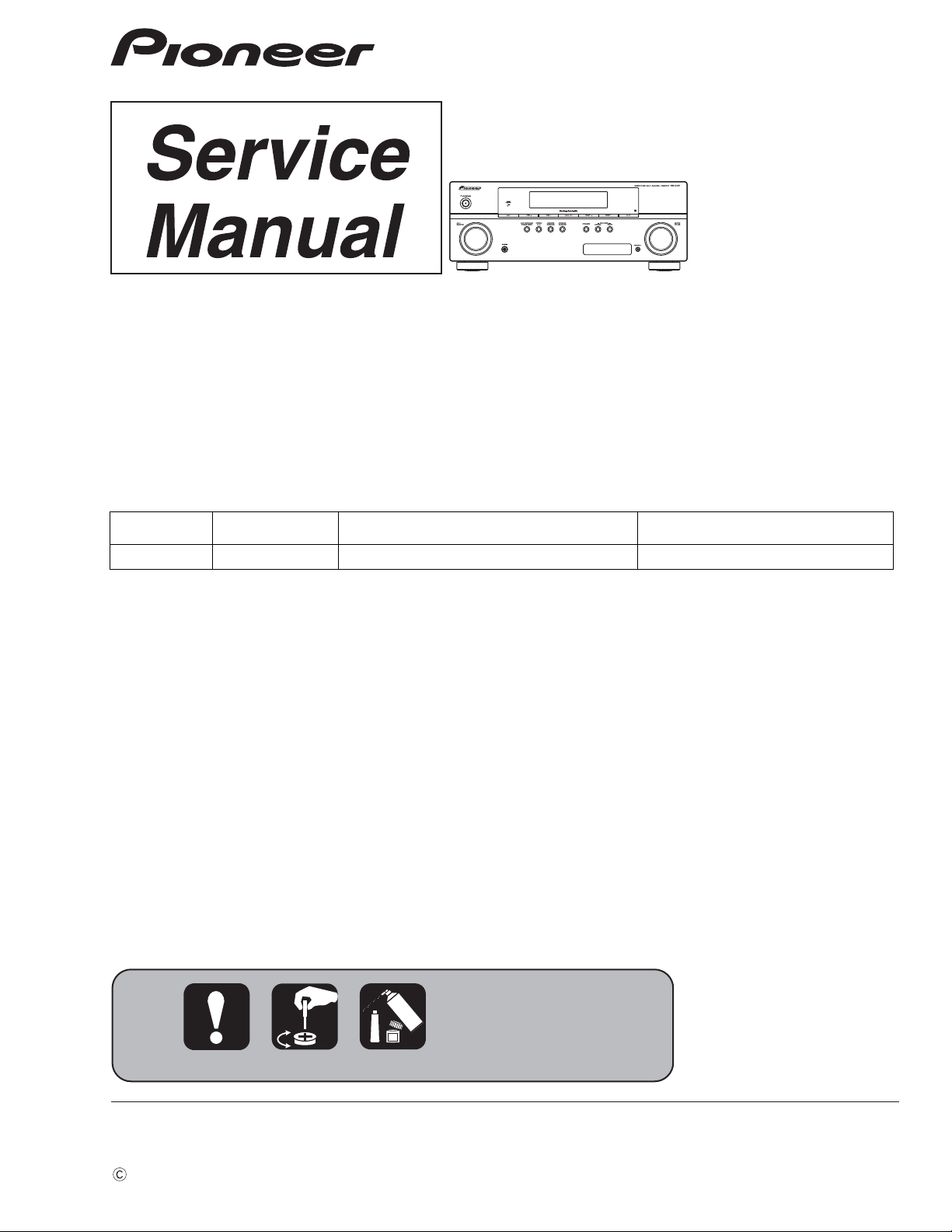
Pioneer VSX-519-K, VSX-519-V Service manual
PIONEER CORPORATION 4-1, Meguro 1-chome, Meguro-ku, Tokyo 153-8654, Japan
PIONEER ELECTRONICS (USA) INC. P.O. Box 1760, Long Beach, CA 90801-1760, U.S.A.
PIONEER EUROPE NV Haven 1087, Keetberglaan 1, 9120 Melsele, Belgium
PIONEER ELECTRONICS ASIACENTRE PTE. LTD. 253 Alexandra Road, #04-01, Singapore 159936
PIONEER CORPORATION
2009
VSX-519V-K
For details, refer to "Important Check Points for good servicing".
AUDIO/VIDEO MULTI-CHANNEL RECEIVER
VSX-519V-K
THIS MANUAL IS APPLICABLE TO THE FOLLOWING MODEL(S) AND TYPE(S).
Model Type Power Requirement Remarks
VSX-519V-K KUCXCN AC 120 V
ORDER NO.
RRV3895
T-ZZK M A R .
2009 Printed in Japan
1
NOTICE
(FOR CANADIAN MODEL ONLY )
Fuse symbols (fast operating fuse) and/or (slow operating fuse) on PCB indicate that replacement parts must
be of identical designation.
REMARQUE
(POUR MODÈLE CANADIEN SEULEMENT)
Les symboles de fusible (fusible de type rapide) et/ou (fusible de type lent) sur CCI indiquent que les pièces
de remplacement doivent avoir la même désignation.
This service manual is intended for qualified service technicians; it is not meant for the casual
do-it-yourselfer. Qualified technicians have the necessary test equipment and tools, and have been
trained to properly and safely repair complex products such as those covered by this manual.
Improperly performed repairs can adversely affect the safety and reliability of the product and may
void the warranty. If you are not qualified to perform the repair of this product properly and safely,
you should not risk trying to do so and refer the repair to a qualified service technician.
WARNING
This product may contain a chemical known to the State of California to cause cancer, or birth defects or other reproductive
harm.
Health & Safety Code Section 25249.6 - Proposition 65
ANY MEASUREMENTS NOT WITHIN THE
LIMITS OUTLINED ABOVE ARE INDICATIVE
OF A POTENTIAL SHOCK HAZARD AND
MUST BE CORRECTED BEFORE RETURNING THE APPLIANCE TO THE CUSTOMER.
2. PRODUCT SAFETY NOTICE
Many electrical and mechanical parts in the appliance
have special safety related characteristics. These are
often not evident from visual inspection nor the
protection afforded by them necessarily can be obtained
by using replacement components rated for voltage,
wattage, etc. Replacement parts which have these
special safety characteristics are identified in this
Service Manual.
Electrical components having such features are
identified by marking with a on the schematics and
on the parts list in this Service Manual.
The use of a substitute replacement component which
does not have the same safety characteristics as the
PIONEER recommended replacement one, shown in the
parts list in this Service Manual, may create shock, fire,
or other hazards.
Product Safety is continuously under review and new
instructions are issued from time to time. For the latest
information, always consult the current PIONEER
Service Manual. A subscription to, or additional copies
of, PIONEER Service Manual may be obtained at a
nominal charge from PIONEER.
(FOR USA MODEL ONLY)
1. SAFETY PRECAUTIONS
The following check should be performed for the
continued protection of the customer and service
technician.
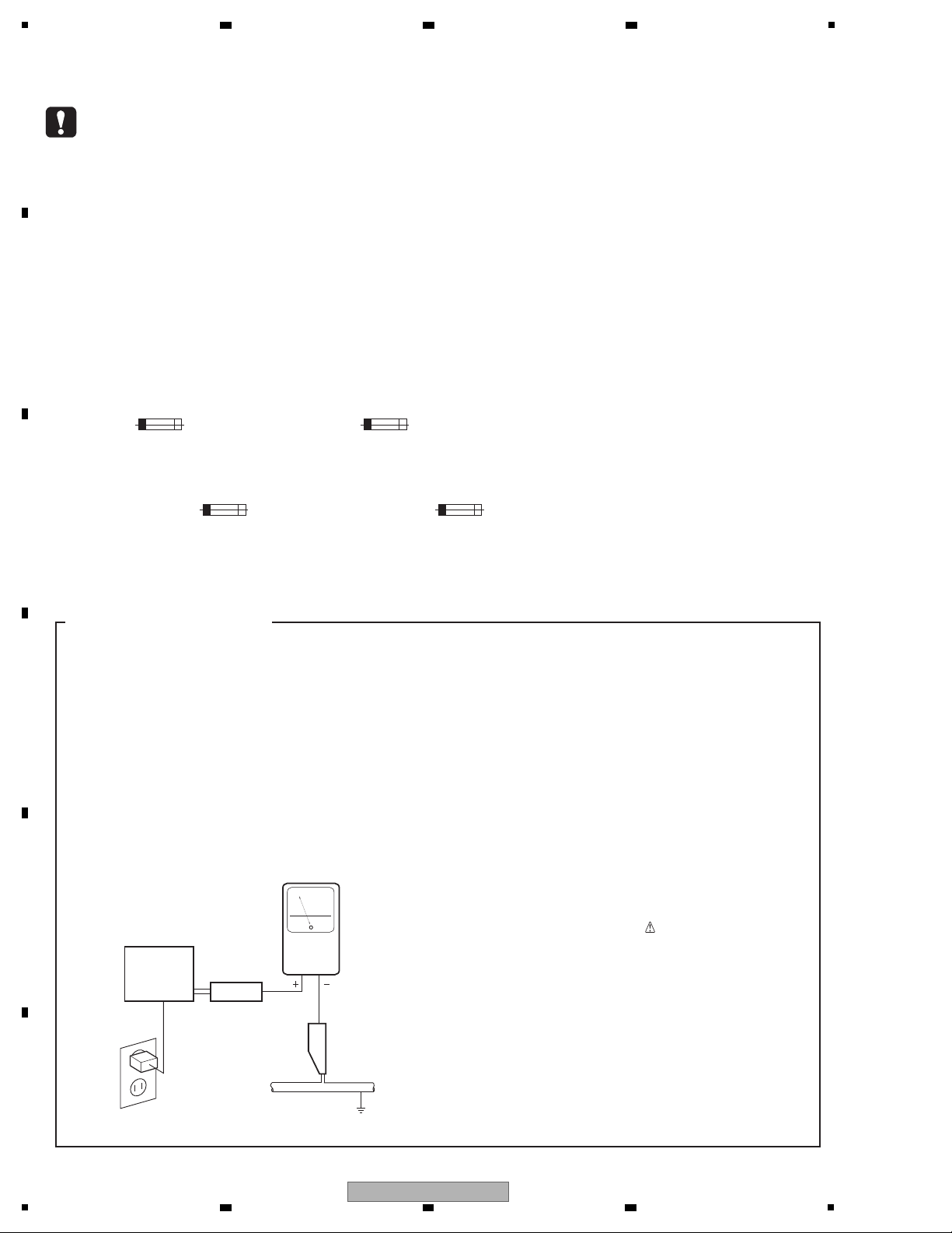
LEAKAGE CURRENT CHECK
Measure leakage current to a known earth ground
(water pipe, conduit, etc.) by connecting a leakage
current tester such as Simpson Model 229-2 or
equivalent between the earth ground and all exposed
metal parts of the appliance (input/output terminals,
screwheads, metal overlays, control shaft, etc.). Plug
the AC line cord of the appliance directly into a 120V
AC 60 Hz outlet and turn the AC power switch on. Any
current measured must not exceed 0.5 mA.
Device
under
test
Leakage
current
tester
Earth
ground
Reading should
not be above
0.5 mA
Also test with
plug reversed
(Using AC adapter
plug as required)
Test al l
exposed metal
surfaces
AC Leakage Test
2 3 4
SAFETY INFORMATION
A
B
C
D
E
F
2
1
2 3 4
VSX-519V-K
5
[Important Check Points for Good Servicing]
In this manual, procedures that must be performed during repairs are marked with the below symbol.
Please be sure to confirm and follow these procedures.
1. Product safety
Please conform to product regulations (such as safety and radiation regulations), and maintain a safe servicing environment by
following the safety instructions described in this manual.
1 Use specified parts for repair.
Use genuine parts. Be sure to use important parts for safety.
2 Do not perform modifications without proper instructions.
Please follow the specified safety methods when modification(addition/change of parts) is required due to interferences such as
radio/TV interference and foreign noise.
3 Make sure the soldering of repaired locations is properly performed.
When you solder while repairing, please be sure that there are no cold solder and other debris.
Soldering should be finished with the proper quantity. (Refer to the example)
4 Make sure the screws are tightly fastened.
Please be sure that all screws are fastened, and that there are no loose screws.
5 Make sure each connectors are correctly inserted.
Please be sure that all connectors are inserted, and that there are no imperfect insertion.
6 Make sure the wiring cables are set to their original state.
Please replace the wiring and cables to the original state after repairs.
In addition, be sure that there are no pinched wires, etc.
7 Make sure screws and soldering scraps do not remain inside the product.
Please check that neither solder debris nor screws remain inside the product.
8 There should be no semi-broken wires, scratches, melting, etc. on the coating of the power cord.
Damaged power cords may lead to fire accidents, so please be sure that there are no damages.
If you find a damaged power cord, please exchange it with a suitable one.
9 There should be no spark traces or similar marks on the power plug.
When spark traces or similar marks are found on the power supply plug, please check the connection and advise on secure
connections and suitable usage. Please exchange the power cord if necessary.
a Safe environment should be secured during servicing.
When you perform repairs, please pay attention to static electricity, furniture, household articles, etc. in order to prevent injuries.
Please pay attention to your surroundings and repair safely.
2. Adjustments
To keep the original performance of the products, optimum adjustments and confirmation of characteristics within specification.
Adjustments should be performed in accordance with the procedures/instructions described in this manual.
4. Cleaning
For parts that require cleaning, such as optical pickups, tape deck heads, lenses and mirrors used in projection monitors, proper
cleaning should be performed to restore their performances.
3. Lubricants, Glues, and Replacement parts
Use grease and adhesives that are equal to the specified substance.
Make sure the proper amount is applied.
5. Shipping mode and Shipping screws
To protect products from damages or failures during transit, the shipping mode should be set or the shipping screws should be
installed before shipment. Please be sure to follow this method especially if it is specified in this manual.
6 7 8
A
B
C
D
5
VSX-519V-K
6 7 8
E
F
3

1
2 3 4
CONTENTS
SAFETY INFORMATION ..........................................................................................................................................................2
1. SERVICE PRECAUTIONS ....................................................................................................................................................5
A
B
C
D
E
1.1 NOTES ON SOLDERING ...............................................................................................................................................5
1.2 CAUTION ........................................................................................................................................................................5
2. SPECIFICATIONS .................................................................................................................................................................6
2.1 SPECIFICATIONS...........................................................................................................................................................6
2.2 PANEL FACILITIES.........................................................................................................................................................7
3. BASIC ITEMS FOR SERVICE.............................................................................................................................................11
3.1 CHECK POINTS AFTER SERVICING..........................................................................................................................11
3.2 PCB LOCATIONS .........................................................................................................................................................12
3.3 JIGS LIST......................................................................................................................................................................13
4. BLOCK DIAGRAM...............................................................................................................................................................14
4.1 OVERALL CONNECTION DIAGRAM...........................................................................................................................14
4.2 AUDIO BLOCK DIAGRAM ............................................................................................................................................16
4.3 VIDEO BLOCK DIAGRAM ............................................................................................................................................18
4.4 U-COM BLOCK DIAGRAM ...........................................................................................................................................19
4.5 POWER SUPPLY BLOCK DIAGRAM ...........................................................................................................................20
5. DIAGNOSIS.........................................................................................................................................................................21
5.1 DIAGNOSIS FLOWCHART...........................................................................................................................................21
5.2 DETECTION CIRCUIT..................................................................................................................................................30
6. SERVICE MODE .................................................................................................................................................................33
6.1 SERVICE MODE...........................................................................................................................................................33
7. DISASSEMBLY....................................................................................................................................................................36
7.1 DISASSEMBLY .............................................................................................................................................................36
8. EACH SETTING AND ADJUSTMENT ................................................................................................................................44
8.1 IDLE CURRENT ADJUSTMENT ..................................................................................................................................44
9. EXPLODED VIEWS AND PARTS LIST...............................................................................................................................46
9.1 PACKING SECTION......................................................................................................................................................46
9.2 EXTERIOR SECTION...................................................................................................................................................48
10. SCHEMATIC DIAGRAM ....................................................................................................................................................52
10.1 P.C.B SUB ASSY (MAIN-519) and P.C.B SUB ASSY (P/T) ........................................................................................52
10.2 P.C.B SUB ASSYS (FRONT), (VOLUME), (FUNCTION), (HEADPHONE) and (PORTABLE)....................................54
10.3 P.C.B SUB ASSY (AMP) .............................................................................................................................................56
10.4 P.C.B SUB ASSY (INPUT) ..........................................................................................................................................58
10.5 P.C.B SUB ASSY (VIDEO-519)...................................................................................................................................60
10.6 P.C.B SUB ASSY (SPEAKER-519) and P.C.B SUB ASSY (CNT)...............................................................................62
10.7 P.C.B SUB ASSY (DSP) (1/2) .....................................................................................................................................64
10.8 P.C.B SUB ASSY (DSP) (2/2) .....................................................................................................................................66
11. PCB CONNECTION DIAGRAM ........................................................................................................................................68
11.1 P.C.B SUB ASSY (MAIN-519) and P.C.B SUB ASSY (P/T) ........................................................................................68
11.2 P.C.B SUB ASSYS (FRONT) ......................................................................................................................................72
11.3 P.C.B SUB ASSYS (VOLUME), (FUNCTION), (HEADPHONE) and (PORTABLE).....................................................74
11.4 P.C.B SUB ASSY (AMP) .............................................................................................................................................76
11.5 P.C.B SUB ASSY (INPUT) ..........................................................................................................................................78
11.6 P.C.B SUB ASSY (VIDEO-519)...................................................................................................................................80
11.7 P.C.B SUB ASSY (SPEAKER-519) .............................................................................................................................84
11.8 P.C.B SUB ASSY (DSP) and P.C.B SUB ASSY (CNT) ...............................................................................................86
11.9 P.C.B SUB ASSY (HDMI-519).....................................................................................................................................90
12. PCB PARTS LIST ..............................................................................................................................................................92
F
4
1
2 3 4
VSX-519V-K

5
• For environmental protection, lead-free solder is used on the printed circuit boards mounted in this unit.
Be sure to use lead-free solder and a soldering iron that can meet specifications for use with lead-free solders for repairs
accompanied by reworking of soldering.
• Compared with conventional eutectic solders, lead-free solders have higher melting points, by approximately 40 ºC.
Therefore, for lead-free soldering, the tip temperature of a soldering iron must be set to around 373 ºC in general, although
the temperature depends on the heat capacity of the PC board on which reworking is required and the weight of the tip of
the soldering iron.
Do NOT use a soldering iron whose tip temperature cannot be controlled.
Compared with eutectic solders, lead-free solders have higher bond strengths but slower wetting times and higher melting
temperatures (hard to melt/easy to harden).
The following lead-free solders are available as service parts:
• Parts numbers of lead-free solder:
GYP1006 1.0 in dia.
GYP1007 0.6 in dia.
GYP1008 0.3 in dia.
• Discharging
For more detail, please refer to “7. DISASSEMBLY - 1. Discharging”.
• Notes on Ground Points Connection
For more detail, please refer to “7. DISASSEMBLY - 2. Notes on Ground Points Connection”.
6 7 8
1. SERVICE PRECAUTIONS
1.1 NOTES ON SOLDERING
A
B
1.2 CAUTION
C
D
E
5
VSX-519V-K
6 7 8
F
5
1
Amplifi er section
Continuous average power output of 80 watts* per
channel, min., at 8 ohms, from 20 Hz to 20 000 Hz with
no more than 0.2 %** total harmonic distortion.
Front (stereo) . . . . . . . . . . . . . . . . . . . . . . . .80 W + 80 W
Power output (1 kHz, 8 Ω, 0.05 %). . . . . 110 W per channel
Guaranteed speaker impedance . . . . . . . . . . . . 6 Ω to 16 Ω
* Measured pursuant to the Federal Trade Commission’s
Trade Regulation rule on Power Output Claims for
Amplifi ers
** Measured by Audio Spectrum Analyzer
Audio Section
Input (Sensitivity/Impedance)
LINE . . . . . . . . . . . . . . . . . . . . . . . . . . . . . . 200 mV/47 kΩ
Output (Level/Impedance)
REC. . . . . . . . . . . . . . . . . . . . . . . . . . . . . . .200 mV/330 Ω
ZONE 2 . . . . . . . . . . . . . . . . . . . . . . . . . . . . .200 mV/1 kΩ
Signal-to-Noise Ratio (IHF, short circuited, A network)
LINE . . . . . . . . . . . . . . . . . . . . . . . . . . . . . . . . . . . . .98 dB
Signal-to-Noise Ratio [EIA, at 1 W (1 kHz)]
LINE . . . . . . . . . . . . . . . . . . . . . . . . . . . . . . . . . . . . .79 dB
Tuner Section
Frequency Range (FM) . . . . . . . . . . . 87.5 MHz to 108 MHz
Antenna Input (FM) . . . . . . . . . . . . . . . . . .75 Ω unbalanced
Frequency Range (AM) . . . . . . . . . . . .530 kHz to 1700 kHz
Antenna (AM) . . . . . . . . . . . . . . . . . . . . . . . . . Loop antenna
Video Section
Signal level
Composite. . . . . . . . . . . . . . . . . . . . . . . . . . 1 Vp-p (75 Ω)
Component Video. . . . . . . . . . . . . . . . . Y: 1.0 Vp-p (75 Ω)
PB, PR: 0.7 Vp-p (75 Ω)
Corresponding maximum resolution
Component Video. . . . . . . . . . . . . . . . . . . . 1080p
(1125p)
Digital I/O
HDMI terminal . . . . . . . . . . . . . . . . . . . . . . 19-pin (Not DVI)
HDMI output type . . . . . . . . . . . . . . . . . . . . . . . .5 V, 100 mA
Integrated control section
Control (IR) terminal. . . . . . . . . . . . . φ 3.5 Mini-jack (MONO)
IR signal . . . . . . . . . . . . . . . High Active (High Level : 2.0 V)
Miscellaneous
Power Requirements . . . . . . . . . . . . . . . . . AC 120 V, 60 Hz
Power Consumption. . . . . . . . . . . . . . . . . . . . . . . . . . 245 W
In standby. . . . . . . . . . . . . . . . . . . . . . . . . . . . . . . . . . .0.5 W
Dimensions . . . 420 mm (W) x 158 mm (H) x 347.7 mm (D)
16
9
/16 in. (W) x 61/4 in. (H) x 133/4 in. (D)
Weight (without package). . . . . . . . . . . . . 8.8 kg (19 lb 7 oz)
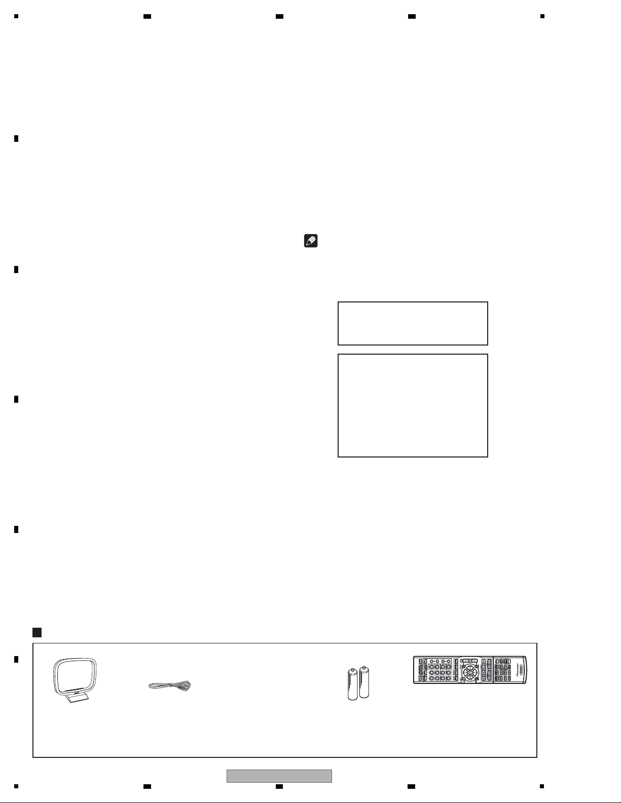
Furnished Parts
Remote control. . . . . . . . . . . . . . . . . . . . . . . . . . . . . . . . . . 1
Dry cell batteries (AAA size IEC R03) . . . . . . . . . . . . . . . . 2
AM loop antenna . . . . . . . . . . . . . . . . . . . . . . . . . . . . . . . . 1
FM wire antenna. . . . . . . . . . . . . . . . . . . . . . . . . . . . . . . . . 1
Operating instructions
Note
Specifi cations and the design are subject to possible
•
modifi cations without notice, due to improvements.
Manufactured under license from Dolby
Laboratories. Dolby, Pro Logic and
the double-D symbol are trademarks
of Dolby Laboratories.
Manufactured under license under U.S.
Patent #’s: 5,451,942; 5,956,674;
5,974,380; 5,978,762; 6,226,616;
6,487,535 & other U.S. and worldwide
patents issued & pending.
DTS and DTS Digital Surround are
registered trademarks and the DTS
logos, Symbol and DTS 96/24 are
trademarks of DTS, Inc. © 1996-2007
DTS, Inc. All Rights Reserved.
Accessories
Remote control
(8300753500010-IL)
AM loop antenna
(E601016000010-IL)
FM wire antenna
(E605010070001-IL)
AAA size IEC R03
Dry cell batteries (x2)
2. SPECIFICATIONS
2.1 SPECIFICATIONS
A
2 3 4
B
C
D
E
F
6
1
VSX-519V-K
2 3 4
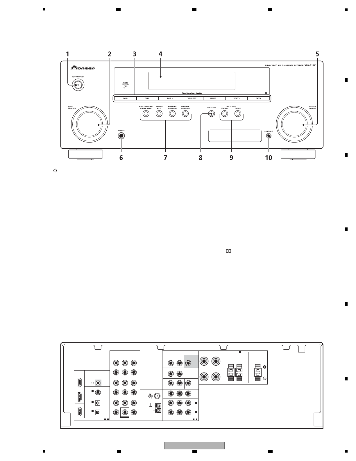
1 STANDBY/ON
2 INPUT SELECTOR dial
Selects an input source.
3 Tuner control buttons
BAND
Switches between AM, FM ST (stereo) and FM MONO
radio bands.
TUNE +/–
Used to fi nd radio frequencies.
TUNER EDIT
Use with TUNE +/–, PRESET +/– and ENTER to
memorize and name stations for recall.
PRESET +/–
Use to select preset radio stations.
4 Character display
5 MASTER VOLUME dial
6 PHONES jack
Use to connect headphones.
7 Listening mode buttons
AUTO SURROUND/STREAM DIRECT
Switches between Auto surround mode and Stream
Direct playback. Stream Direct playback bypasses the
tone controls for the most accurate reproduction of a
source .
STEREO/A.L.C.
Switches between stereo playback, Auto level control
stereo mode and Front Stage Surround Advance
modes.
ADVANCED SURROUND
Switches between the various surround modes.
STANDARD SURROUND
Press for Standard decoding and to switch between the
various
Pro Logic II options.
8 SPEAKERS
Use to change the speaker system on or off.
9 MULTI ZONE controls
If you’ve made MULTI-ZONE connections use these
conrols to control the sub zone from the main zone.
10 PORTABLE audio input jack
Connect an auxiliary component using a stereo mini-jack
cable.
Rear panel
Front panel
AUDIO
AUDIO
DIGITAL
COMPONENT VIDEO
BD/DVD MULTI CH IN
BD/DVD IN
HDMI
ANTENNA
AM
LOOP
FRONT
L
R
L
R
CENTERSURROUND
COAXIAL
(CD)
IN 1
Class 2 Wiring
SPEAKERS A
(CD-R/TAPE)
IN 1
1-2
(DVR/VCR)
IN 2
(BD/DVD)
IN 1
(TV/SAT)
IN 2
OPTICAL
ASSIGNABLE
IR
ASSIGNABLE
1-2
ASSIGNABLE
OUT
OUT
YPBP
R
IN
FRONT
ZONE2 OUT
MONITOR OUT BD/DVD IN TV/SAT IN
RL
SURROUND CENTER
SUBWOOFER
PRE OUT
L R
DVR/VCR TV/SAT
OUT
IN
DVR/VCR VIDEO
L
R
OUT
BD/DVD
IN
TV/SAT
IN
OUT
IN IN
IN
CD-R/TAPE CD
SUBWOOFER
IN
RL
5
2.2 PANEL FACILITIES
6 7 8
A
B
C
D
E
5
VSX-519V-K
F
7
6 7 8
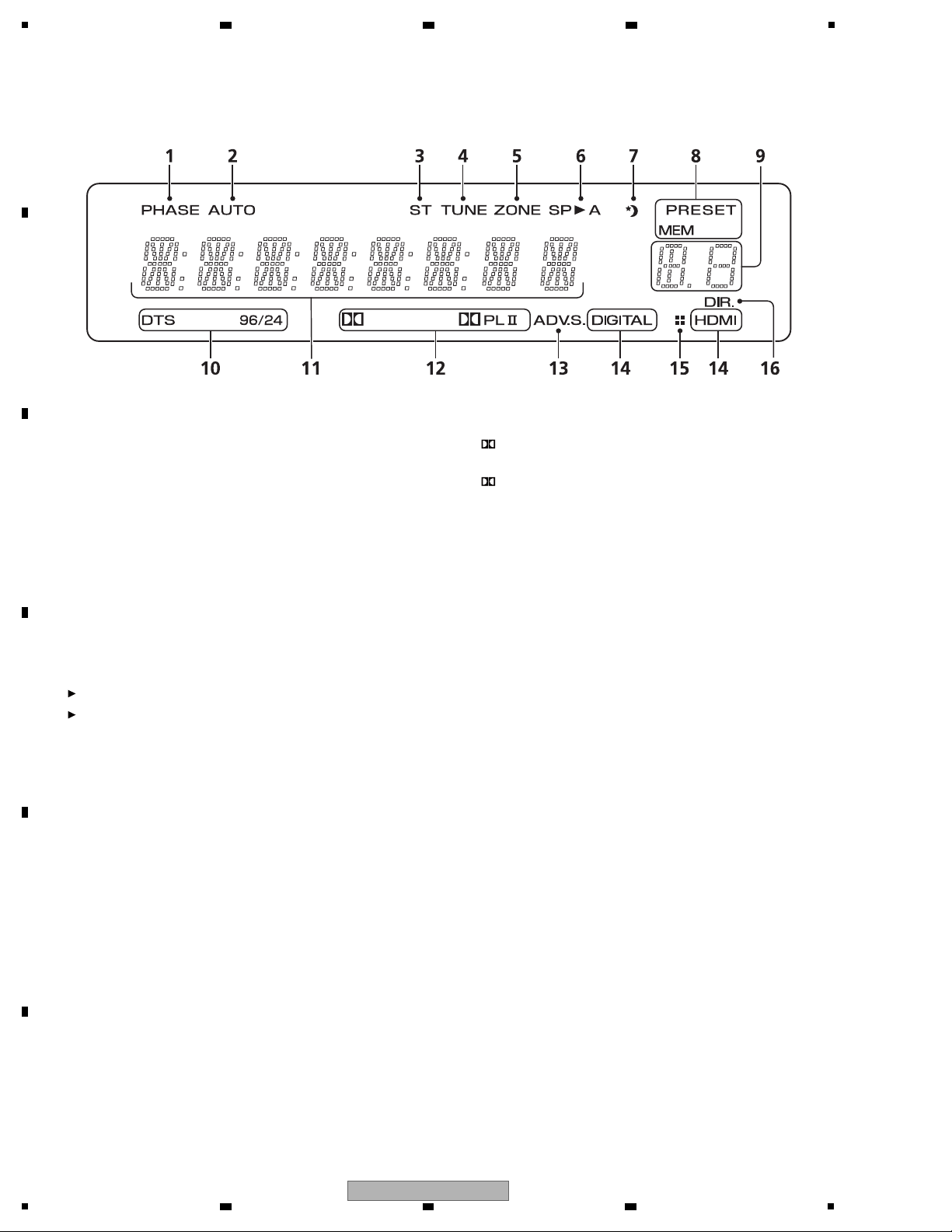
A
1 PHASE
Lights when the Phase Control is switched on.
2 AUTO
Lights when the Auto Surround feature is switched on.
3 ST
Lights when a stereo FM broadcast is being received in
auto stereo mode.
4 TUNE
Lights when a broadcast is being received.
5 ZONE
Lights when the MULTI-ZONE feature is active.
6 Speaker indicator
Shows if the speaker system is on or not.
SP
A means the speakers are switched on.
SP
means the speakers are switched off and sound is
output from the headphone jack.
7 Sleep timer indicator
Lights when the receiver is in sleep mode.
8 Tuner preset indicators
PRESET
Shows when a preset radio station is registered or
called.
MEM
Blinks when a radio station is registered.
9 PRESET information or input signal indicator
Shows the preset number of the tuner or the input signal
type etc.
10 DTS indicators
DTS
Lights when a source with DTS encoded audio signals
is detected.
96/24
Lights when a source with DTS 96/24 encoded audio
signals is detected.
11 Character display
Displays various system information.
12 Dolby Digital indicators
Lights when a Dolby Digital encoded signal is detected.
PLll
Lights to indicate Pro Logic II decoding.
13 ADV.S.
Lights when one of the Advanced Surround modes has
been selected.
14 SIGNAL SELECT indicators
DIGITAL
Lights when a digital audio signal is selected.
Blinks when a digital audio signal is not selected.
HDMI
Lights when an HDMI signal is selected.
Blinks when an HDMI signal is not selected.
15 DIMMER indicator
Shows when the display is set to turn off as the DIMMER
setting.
16 DIR.
Lights when the DIRECT or PURE DIRECT mode is
switched on.
Display
B
1
2 3 4
C
D
E
F
8
1
2 3 4
VSX-519V-K
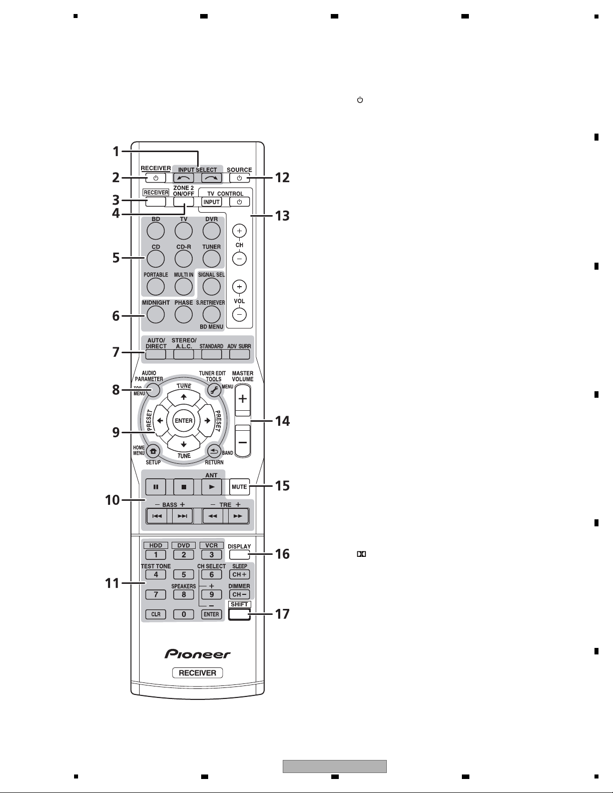
5
Remote control
As for operating other devices, the remote control codes
for the Pioneer products are preset. The settings cannot be
changed.
1 INPUT SELECT
Use to select the input source.
2
RECEIVER
Switches the receiver between standby and on.
3 RECEIVER
Switches the remote to control the receiver (used to select
the white commands above the number buttons (TEST
TONE, etc)). Also use this button to set up surround sound
or Audio parameters.
4 ZONE 2 ON /OFF
Switches zone 2 of the multi-zone function between on and
off.
5 MULTI CONTROL buttons
Press to select control of other components.
6 Receiver control buttons
SIGNAL SEL
Use to select an input signal.
MIDNIGHT
Switches to Midnight or Loudness listening.
PHASE
Press to switch on/off Phase Control.
S.RETRIEVER
Press to restore CD quality sound to compressed audio
sources.
Press BD fi rst to access:
BD MENU
Displays the disc menu of Blu-ray Discs.
7 Listening mode buttons
AUTO /DIRECT
Switches between Auto surround mode and Stream
Direct playback. Stream Direct playback bypasses the
tone controls for the most accurate reproduction of a
source.
STEREO/A.L.C.
Switches between stereo playback, Auto level control
stereo mode and Front Stage Surround Advance
modes.
STANDARD
Press for Standard decoding and to switch between
Pro Logic II options.
ADV SURR
Switches between the various surround modes.
8 System Setup and Component control buttons
The following button controls can be accessed after you
have selected the corresponding MULTI CONTROL button
(BD, TV, etc.).
Press RECEIVER fi rst to access:
AUDIO PARAMETER
Use to access the Audio options.
SETUP
Press to access the System Setup menu.
RETURN
Confi rm and exit the current menu screen.
Press BD or DVR fi rst to access:
TOP MENU
6 7 8
A
5
6 7 8
VSX-519V-K
B
C
D
E
F
9

1
Displays the disc ‘top’ menu of a BD/DVD.
HOME MENU
Displays the HOME MENU screen.
RETURN
Confi rm and exit the current menu screen.
MENU
Displays the TOOLS menu of Blu-ray Disc player.
Press TUNER fi rst to access:
T.E DIT
Memorizes/names stations for recall.
BAND
Switches between AM, FM ST (stereo) and FM MONO
radio bands.
9
(TUNE / , PRESET / ), ENTER
Use the arrow buttons when setting up your surround sound
system. Also used to control BD/DVD menus/options.
Use the TUNE
/ buttons can be used to fi nd radio
frequencies and the PRESET
/ buttons can be used to
select preset radio stations.
10 Component control buttons
The main buttons (
, , etc.) are used to control a
component after you have selected it using the input source
buttons.
The controls above these buttons can be accessed after
you have have selected the corresponding input source
button (for example BD, DVR or TV). These buttons also
function as described below.
Press RECEIVER fi rst to access:
BASS – /+
Use to adjust Bass
1
TRE – /+
Use to adjust Treble
1
Press TV fi rst to access:
ANT
Use to select the VHF/UHF antennas or Cable TV.
11 Number buttons and other component controls
Use the number buttons to directly select the tracks on
a CD, DVD, etc. There are other buttons that can be
accessed after the RECEIVER button is pressed. (For
example TEST TONE, etc.)
HDD*, DVD*, VCR*
These buttons switch between the hard disk, DVD and
VCR controls for HDD/DVD/VCR recorders.
TEST TONE
Outputs the test tones on each channel. Use the
/
buttons to select the channel and use the
/ buttons
to adjust the level on each channel. Pressing TEST
TONE again exits the test tone mode.
CH SELECT
Press repeatedly to select a channel, then use +/– to
adjust the level.
CH SELECT +/–
Use to adjust the channel levels.
SPEAKERS
Use to change the speaker system on or off.
SLEEP
Press to change the amount of time before the receiver
switches into standby (30 min – 60 min – 90 min –
Off). You can check the remaining sleep time at any
time by pressing SLEEP once.
DIMMER
Dims or brightens the display. The brightness can be
controlled in four steps.
12
SOURCE
Turns on or off the power of the Pioneer DVD/DVR units
when BD or DVR is selected using the MULTI CONTROL
buttons.
13 TV CONTROL buttons
These buttons can control only be used with Pioneer fl at
panel TVs.
Use to turn on/off the power of the TV.
INPUT
Use to select the TV input signal.
CH +/–
Use to select channels.
VOL +/ –
Use to adjust the volume on your TV.
14 MASTER VOLUME +/–
Use to set the listening volume.
15 MUTE
Mutes/unmutes the sound.
16 DISPLAY
Switches the display of this unit. The input name, listening
mode or sound volume can be checked by selecting an
input source.
17 SHIFT
Press to access the ‘boxed’ commands (above the buttons)
on the remote. These buttons are marked with an asterisk
(* ) in this section. This button is also used for operating
ZONE 2.
Note
1 The tone controls are disabled when the listening mode
is set to DIRECT or PURE DIRECT.
A
2 3 4
B
C
D
E
F
10
1
2 3 4
VSX-519V-K
5
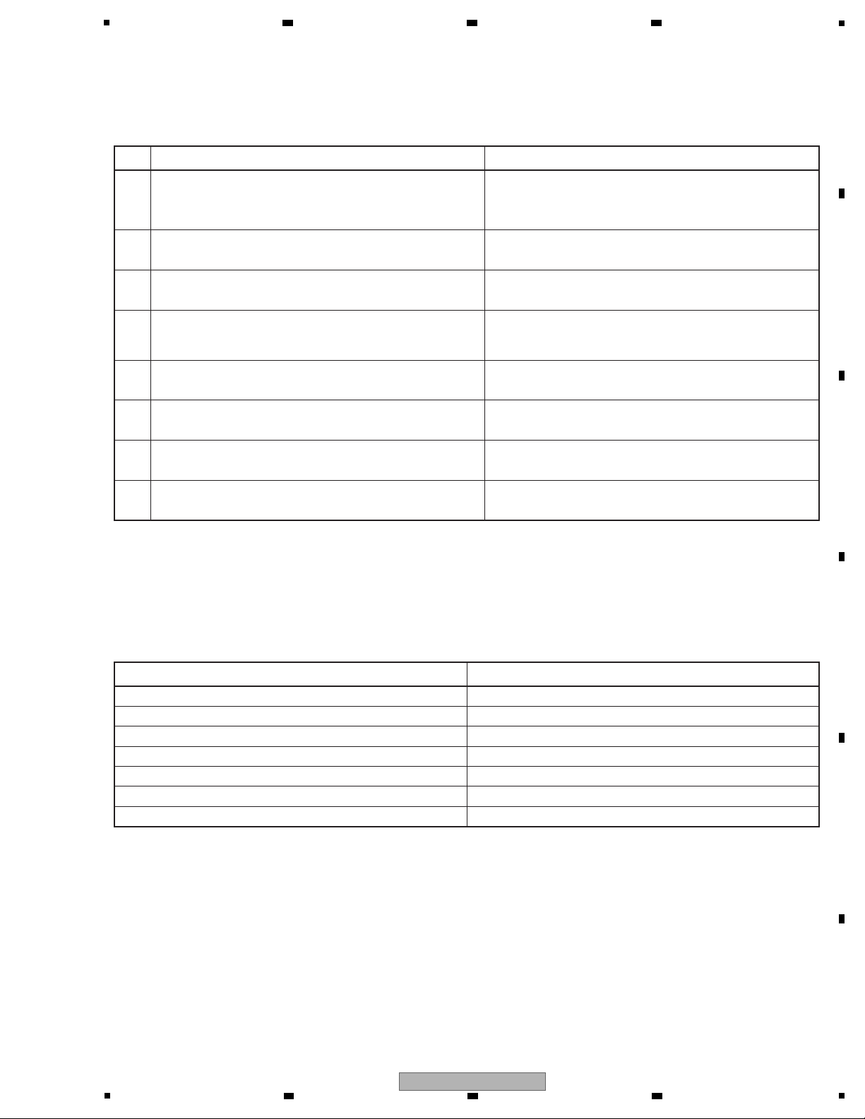
Item to be checked regarding video Item to be checked regarding audio
Block noise Distortion
Horizontal noise Noise
Flicker Volume too low
Disturbed image (video jumpiness) Volume too high
Too dark Volume fluctuating
Too bright Sound interrupted
Mottled color
No. Procedures Check points
1
2
3
4
5
6
7
8
Confirm whether the customer complain has been solved.
If the customer complain occurs with the particular source,
such as Dolby Digital, DTS, AAC, DVD-A and HDMI, input it for
the operation check.
The customer complain must not be reappeared.
Video, Audio and operations must be normal.
Check the analog audio playback.
(Make the analog connections with a DVD player.)
Each channel audio and operations must be normal.
Check the digital audio playback.
(Make the digital connections with a DVD player.)
Each channel audio and operations must be normal.
Check surround playback.
(Select Surround mode and check the multichannel operations
via the DSP circuit.)
Each channel audio and operations must be normal.
Check the tuner (AM and FM) operations. Audio and operations must be normal.
Check the video outputs.
(Connect with a DVD player.)
Video and operations must be normal.
Check the sound from headphone output. Sound must be normal, without noise.
Check the appearance of the product. No scratches or dirt on its appearance after receiving it for
service.
Items to be checked after servicing / VSX, SC
To keep the product quality after servicing, confirm recommended check points shown below.
See the table below for the items to be checked regarding video and audio.
6 7 8
3. BASIC ITEMS FOR SERVICE
3.1 CHECK POINTS AFTER SERVICING
A
B
C
D
E
F
VSX-519V-K
5
6 7 8
11
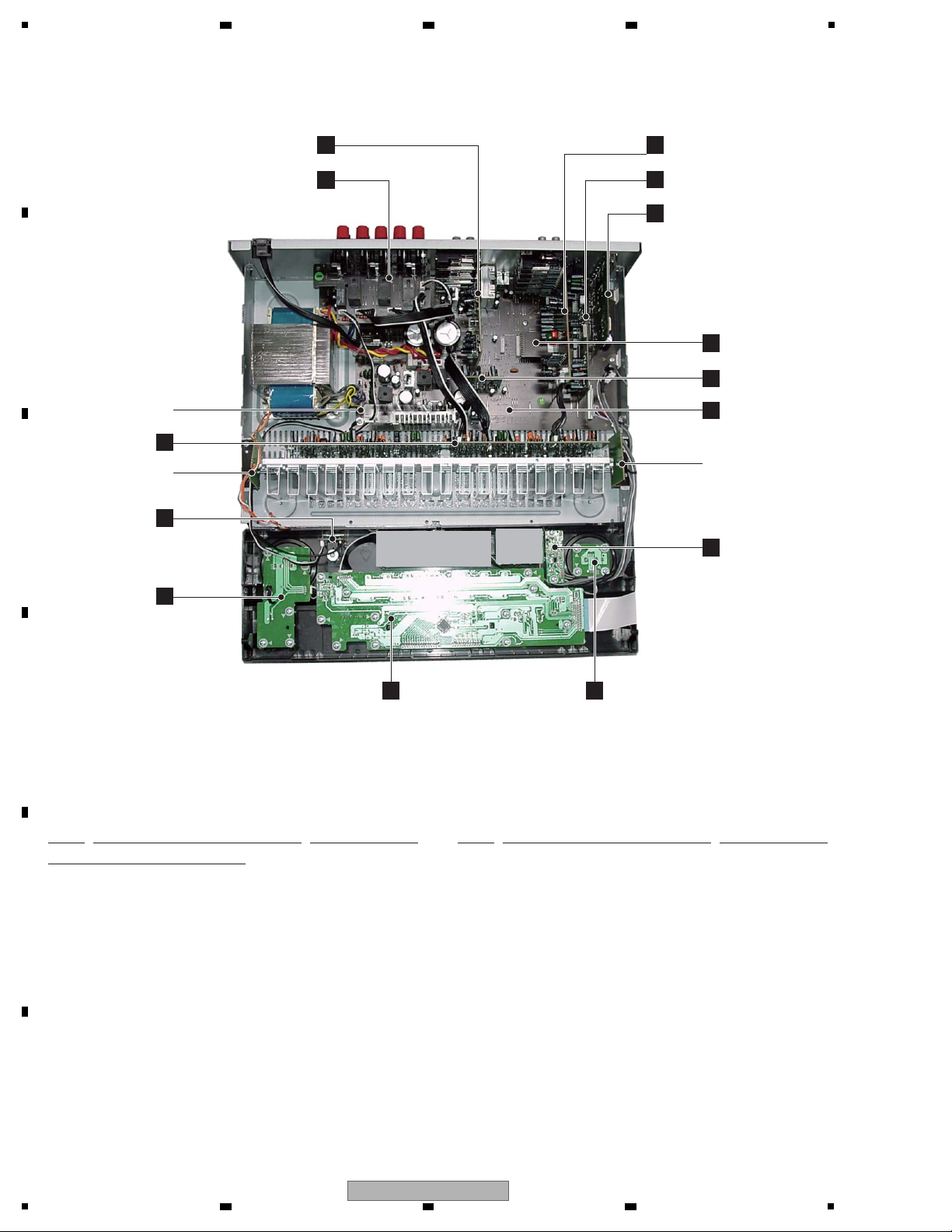
1
C
P.C.B SUB ASSY
(FRONT)
D
P.C.B SUB ASSY
(VOLUME)
P.C.B SUB ASSY
(GUIDE PCB R)
A
P.C.B SUB ASSY
(MAIN-519)
B
P.C.B SUB ASSY
(P/T)
P.C.B SUB ASSY
(FUNCTION)
E
P.C.B SUB ASSY
(AMP)
J
P.C.B SUB ASSY
(GUIDE PCB L)
P
P.C.B SUB ASSY
(DSP)
K
P.C.B SUB ASSY
(INPUT)
L
P.C.B SUB ASSY
(VIDEO-519)
M
P.C.B SUB ASSY
(SPEAKER-519)
Mark No. Description Part No. Mark No. Description Part No.
LIST OF ASSEMBLIES
NOTES: - Parts marked by “NSP” are generally unavailable because they are not in our Master Spare Parts List.
-
The > mark found on some component parts indicates the importance of the safety factor of the part.
Therefore, when replacing, be sure to use parts of identical designation.
P.C.B SUB ASSY
(HEADPHONE)
F
N
P.C.B SUB ASSY
(CNT)
> NSP 1..P.C.B TOTAL ASSY (AMP) 7025HK0811012-IL
2..P.C.B SUB ASSY (AMP) 7028067521010-IL
NSP 1..P.C.B TOTAL ASSY (FRONT) 7025HK0812011-IL
2..P.C.B SUB ASSY (FRONT) 7028067511020-IL
2..P.C.B SUB ASSY (HEADPHONE) 7028067512010-IL
2..P.C.B SUB ASSY (VOLUME) 7028067513010-IL
2..P.C.B SUB ASSY (FUNCTION) 7028067514010-IL
2..P.C.B SUB ASSY (PORTABLE) 7028067518010-IL
NSP 1..P.C.B TOTAL ASSY (INPUT) 7025HK0812013-IL
2..P.C.B SUB ASSY (INPUT) 7028067531020-IL
NSP 1..P.C.B TOTAL ASSY (VIDEO-519) 7025HK0812014-IL
2..P.C.B SUB ASSY (VIDEO-519) 7028067551010-IL
NSP 1..P.C.B TOTAL ASSY (DSP) 7025HK0812015-IL
2..P.C.B SUB ASSY (DSP) 7028067561020-IL
NSP 1..P.C.B TOTAL ASSY (HDMI-519) 7025HK0812016-IL
2..P.C.B SUB ASSY (HDMI-519) 7028067581010-IL
NSP 1..P.C.B TOTAL ASSY (MAIN-519) 7025HK0812020-IL
2..P.C.B SUB ASSY (MAIN-519) 7028067501080-IL
2..P.C.B SUB ASSY (GUIDE-L) 7028067502010-IL
2..P.C.B SUB ASSY (GUIDE-R) 7028067503010-IL
2..P.C.B SUB ASSY (CNT) 7028067504010-IL
2..P.C.B SUB ASSY (P/T) 7028067505010-IL
2..P.C.B SUB ASSY (H/P GUIDE) 7028067506010-IL
NSP 1..P.C.B TOTAL ASSY (SPEAKER-519) 7025HK0812021-IL
2..P.C.B SUB ASSY (SPEAKER-519) 7028067601040-IL
Q
P.C.B SUB ASSY
(HDMI-519)
I
P.C.B SUB ASSY
(PORTABLE)
P.C.B SUB ASSY
(H/P GUIDE)
3.2 PCB LOCATIONS
A
2 3 4
B
C
D
E
F
12
1
2 3 4
VSX-519V-K
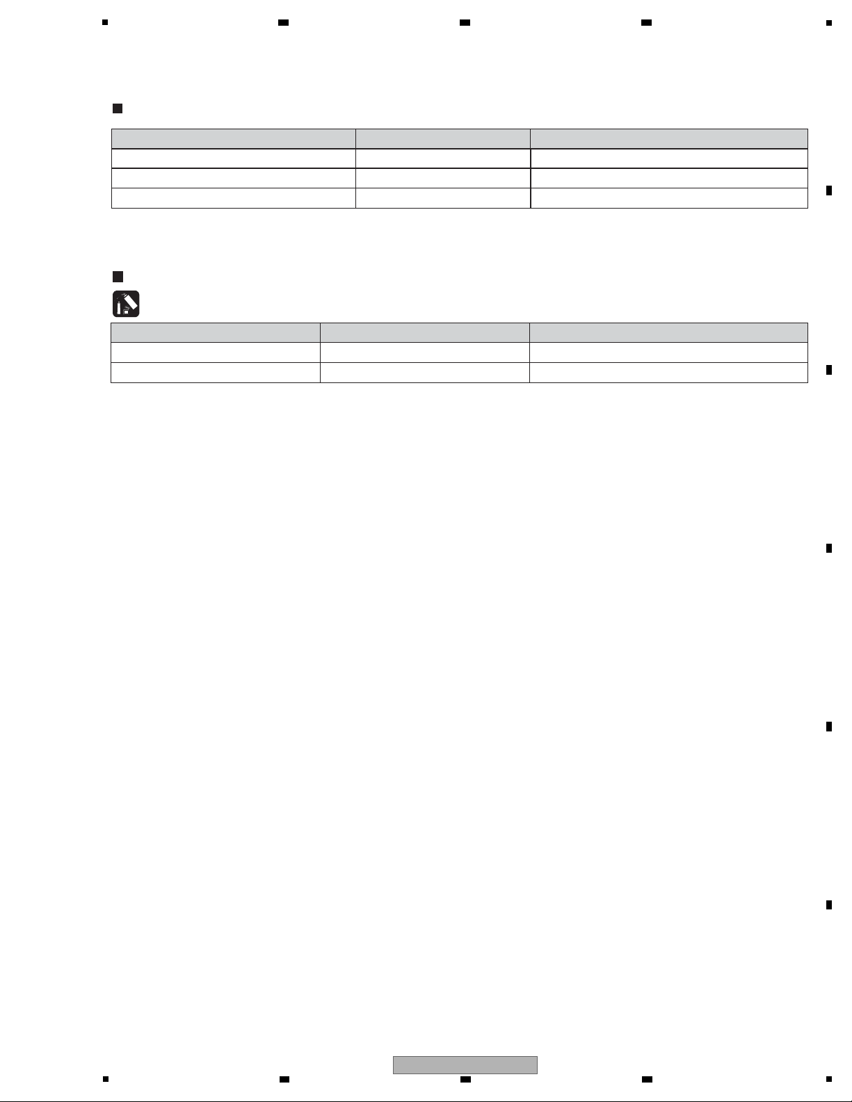
5
Silicon grease GEM1057
GYA1011 (KE40RTV-W)
Silicon adhesive
Name Lubricants and Glues No. Remarks
Refer to "9.2 EXTERIOR SECTION"
Refer to "9.2 EXTERIOR SECTION"
Lubricants and Glues list
Name Jig No. Remarks
10P extension jig
cable GGD1628
Diagnosis
8P extension jig cable
GGD1629
Diagnosis
Board to board extension jig cable
GGD1630
Diagnosis
Jigs list
3.3 JIGS LIST
6 7 8
A
B
C
D
E
F
VSX-519V-K
5
6 7 8
13
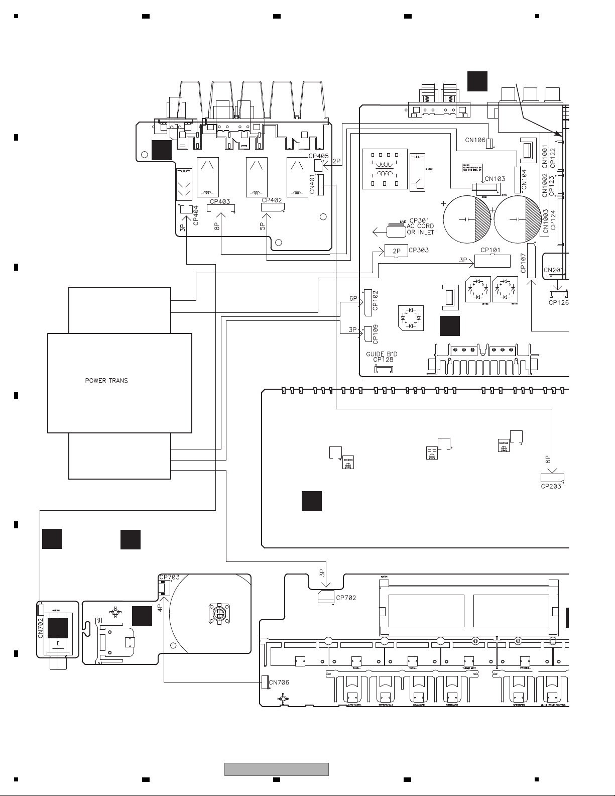
1
P.C.B SUB ASSY
L
P.
(7
P.C.B SUB ASSY
(FUNCTION)
(7028067514010-IL)
E
E
P.C.B SUB
ASSY
(HEADPHONE)
(7028067512010-IL)
F
F
P.C.B SUB ASSY
(SPEAKER-519)
(7028067601040-IL)
M
P.C.B SUB ASSY
(7028067501080-IL
A
P.C.B SUB ASSY (AMP)
(7028067521010-IL)
J
P
A
(
2 3 4
4. BLOCK DIAGRAM
4.1 OVERALL CONNECTION DIAGRAM
A
B
C
D
E
F
14
1
VSX-519V-K
2 3 4
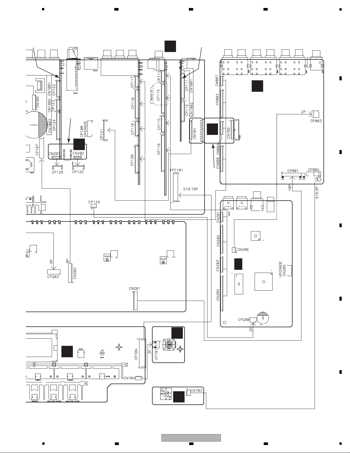
5
P.C.B SUB ASSY (FRONT)
(7028067511020-IL)
C
P.C.B SUB ASSY
(VOLUME)
(7028067513010-IL)
D
P.C.B SUB ASSY
(CNT)
(7028067504010-IL)
N
P.C.B SUB ASSY
(INPUT)
(7028067531020-IL)
K
P.C.B SUB ASSY (HDMI-519)(7028067581010-IL)
Q
P 1/2,2/2
P.C.B SUB ASSY (DSP)
(7028067561020-IL)
SUB ASSY (MAIN-519)
67501080-IL)
P.C.B SUB
ASSY (P/T)
(7028067505010-IL)
B
P.C.B SUB ASSY (PORTABLE)
(7028067518010-IL)
I
6 7 8
A
B
C
D
E
5
6 7 8
VSX-519V-K
F
15
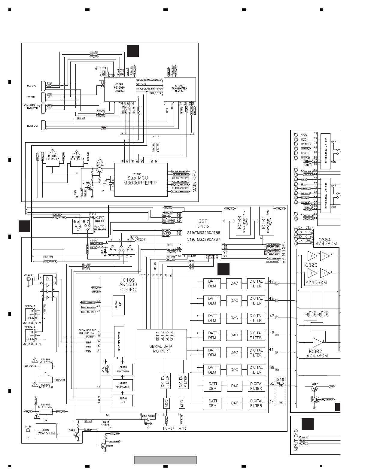
1
I
P.C.B SUB ASSY
(HDMI-519)
Q
P.C.B SUB ASSY
(DSP)
P.C.B SUB
ASSY (MAIN)
A
P
K
P.C.B SUB
(PORTABL
4.2 AUDIO BLOCK DIAGRAM
A
B
2 3 4
C
D
E
F
16
1
2 3 4
VSX-519V-K
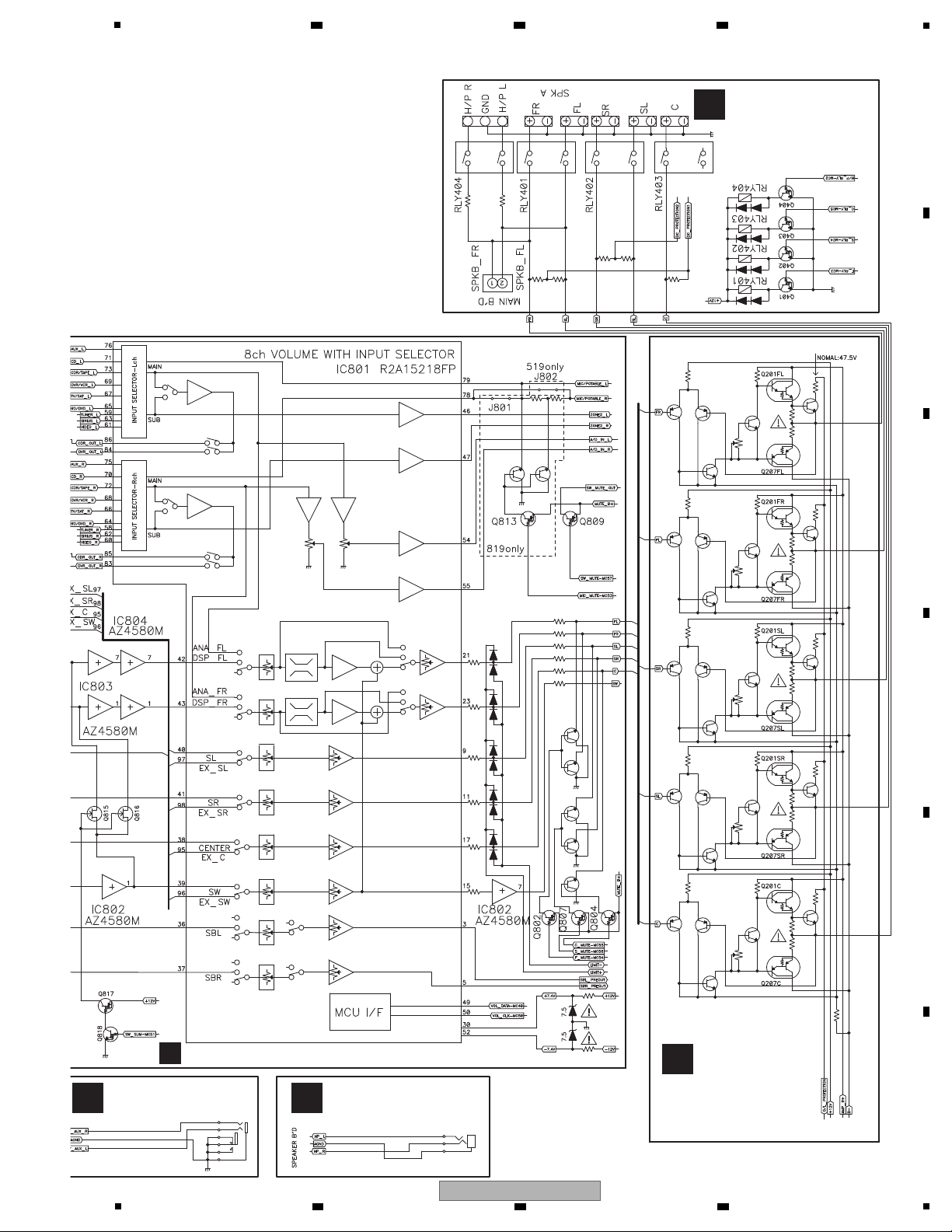
5
P.C.B SUB ASSY
(HEADPHONE)
FI
P.C.B SUB ASSY (INPUT)
P.C.B SUB ASSY
(AMP)
J
P.C.B SUB ASSY
(SPEAKER-519)
M
K
P.C.B SUB ASSY
(PORTABLE)
6 7 8
A
B
C
D
E
5
VSX-519V-K
6 7 8
F
17
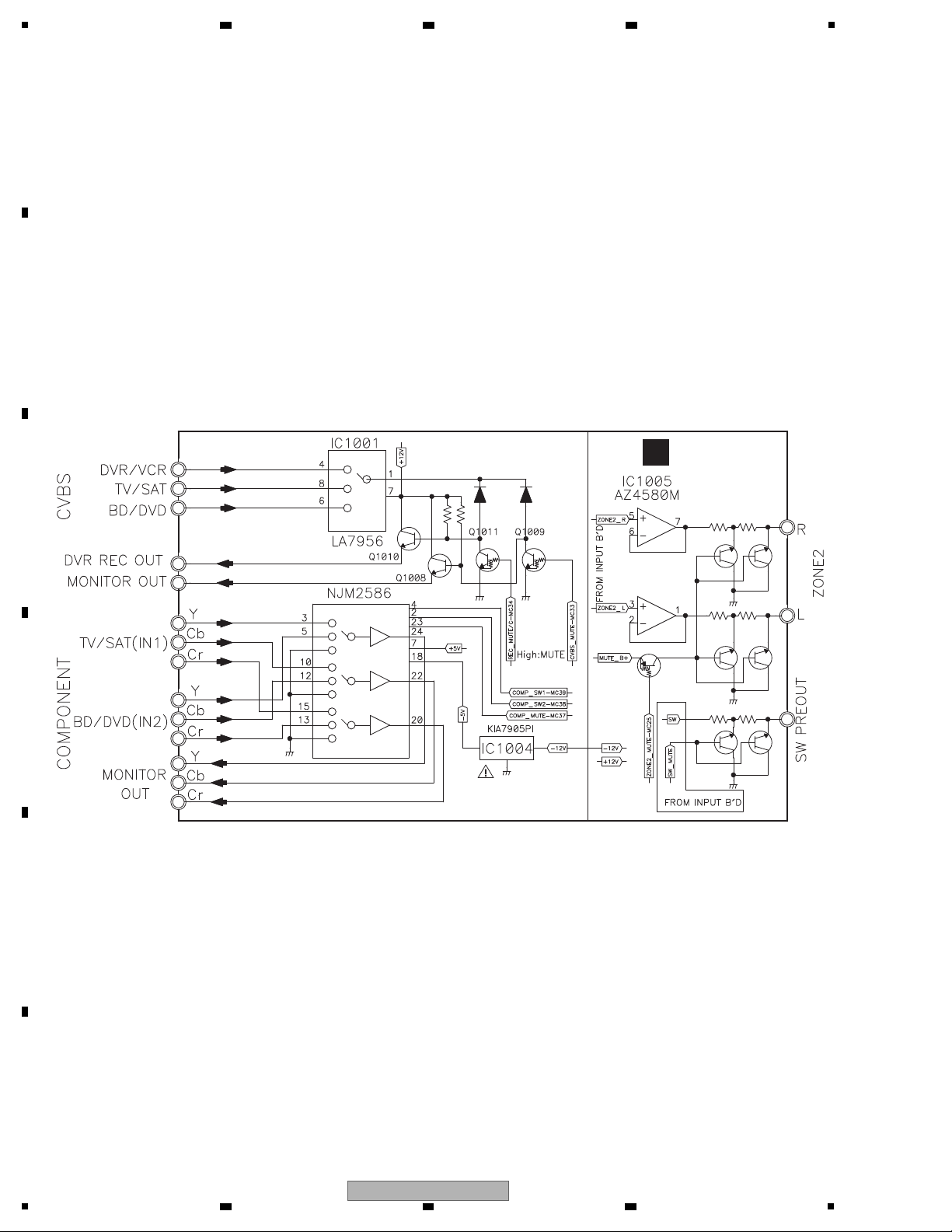
1
P.C.B SUB ASSY
(VIDEO-519)
L
4.3 VIDEO BLOCK DIAGRAM
A
B
2 3 4
C
D
E
F
18
1
2 3 4
VSX-519V-K
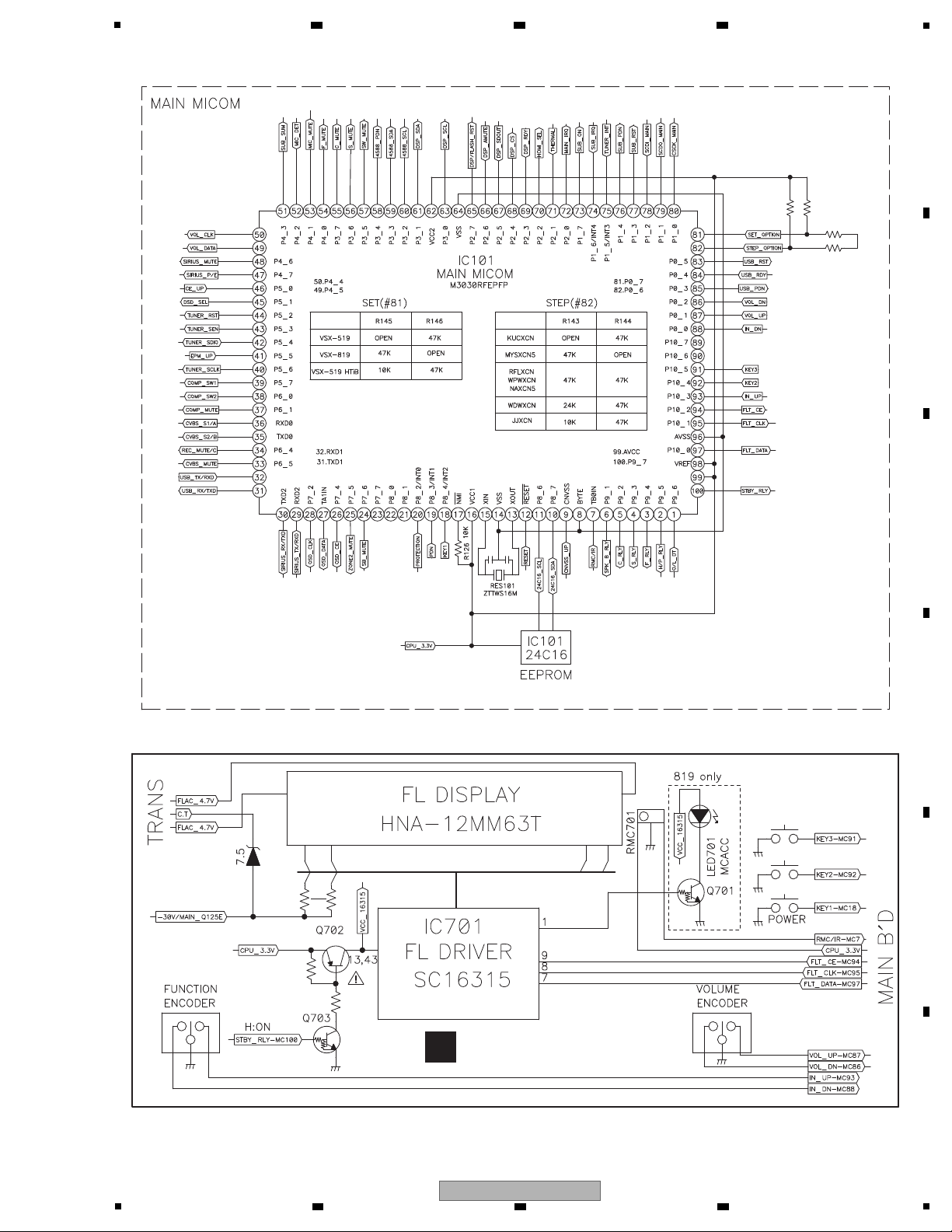
5
P.C.B SUB ASSY
(FRONT)
C
4.4 U-COM BLOCK DIAGRAM
6 7 8
A
B
C
D
E
VSX-519V-K
5
6 7 8
F
19
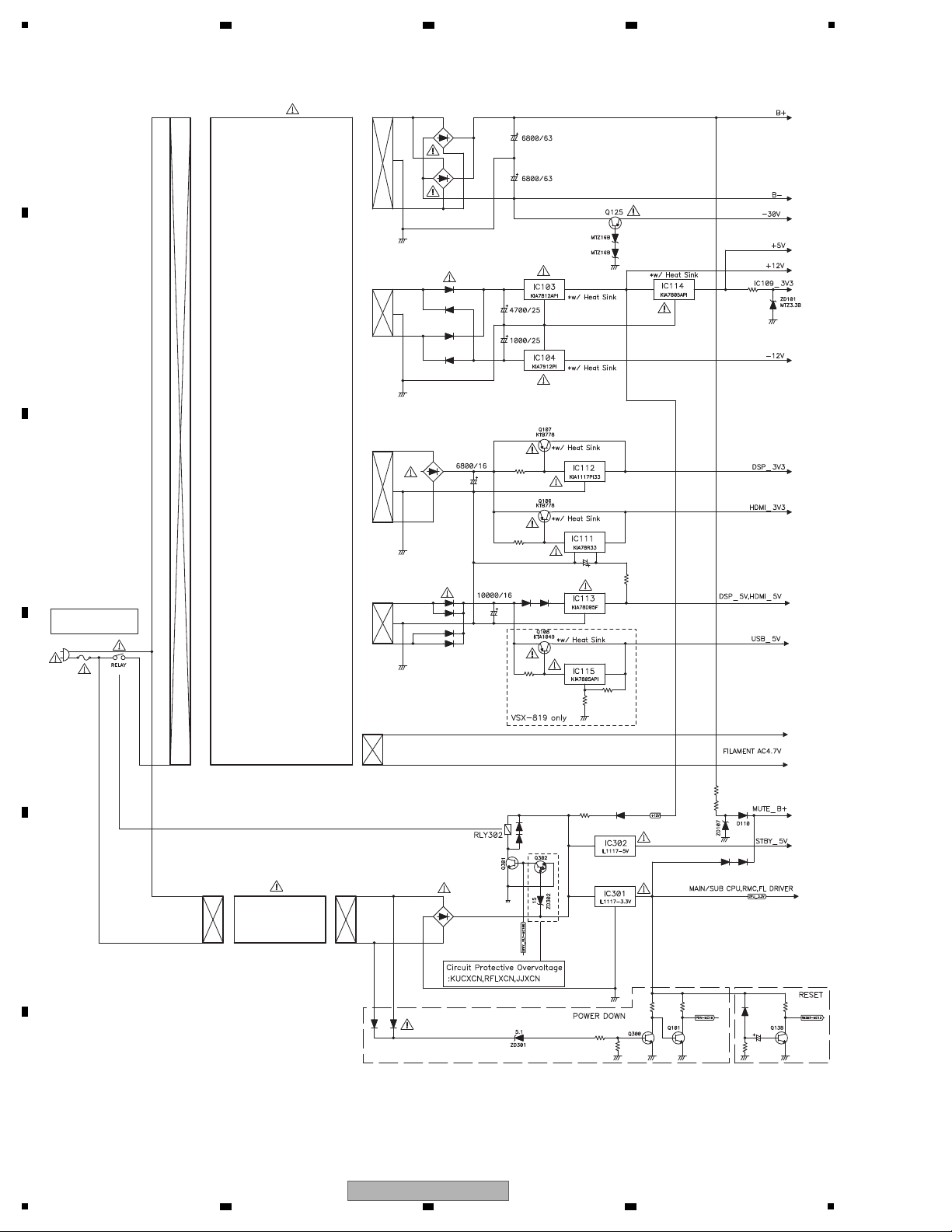
1
S4(FLT)
S3(DSP, HDMI)
AC CORD
S2(+12V,-12V)
S1(AMP B+/B-)
S4(DIR/CODEC, HDMI, USB)
MAIN TRANS
SUB TRANS
2 3 4
4.5 POWER SUPPLY BLOCK DIAGRAM
A
B
C
D
E
F
20
1
2 3 4
VSX-519V-K
5
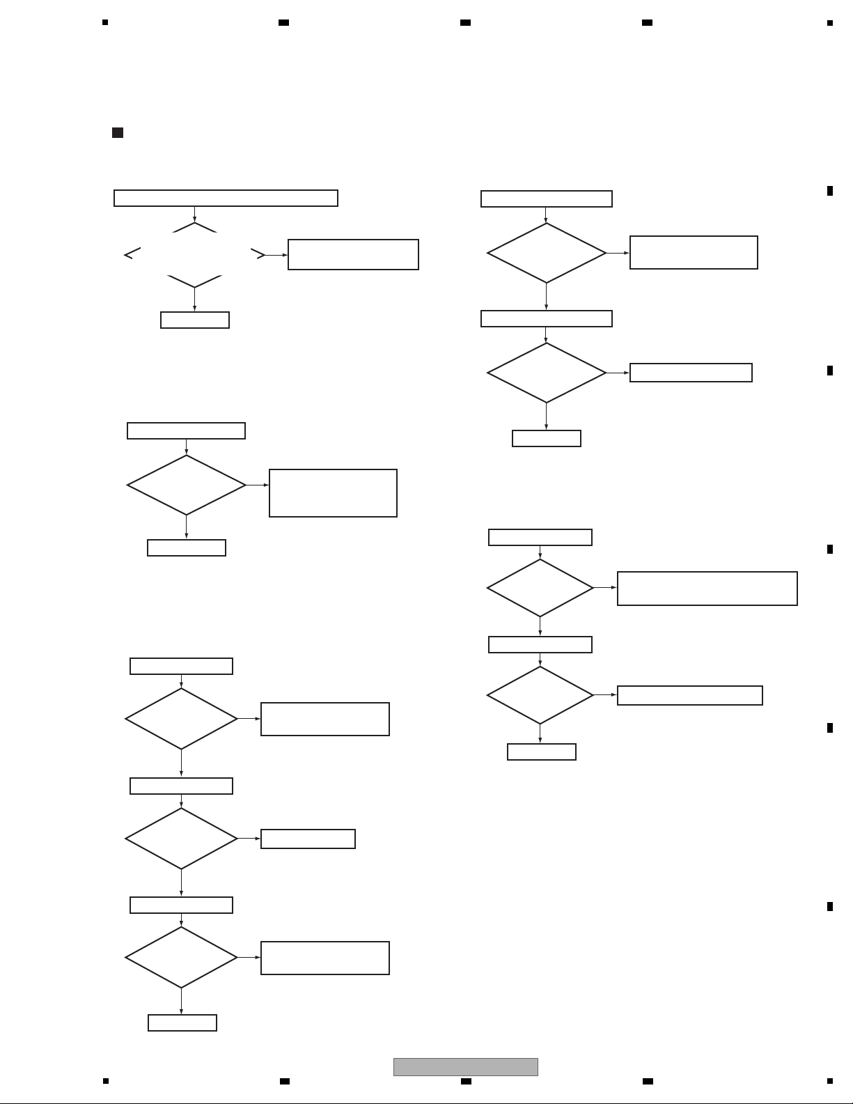
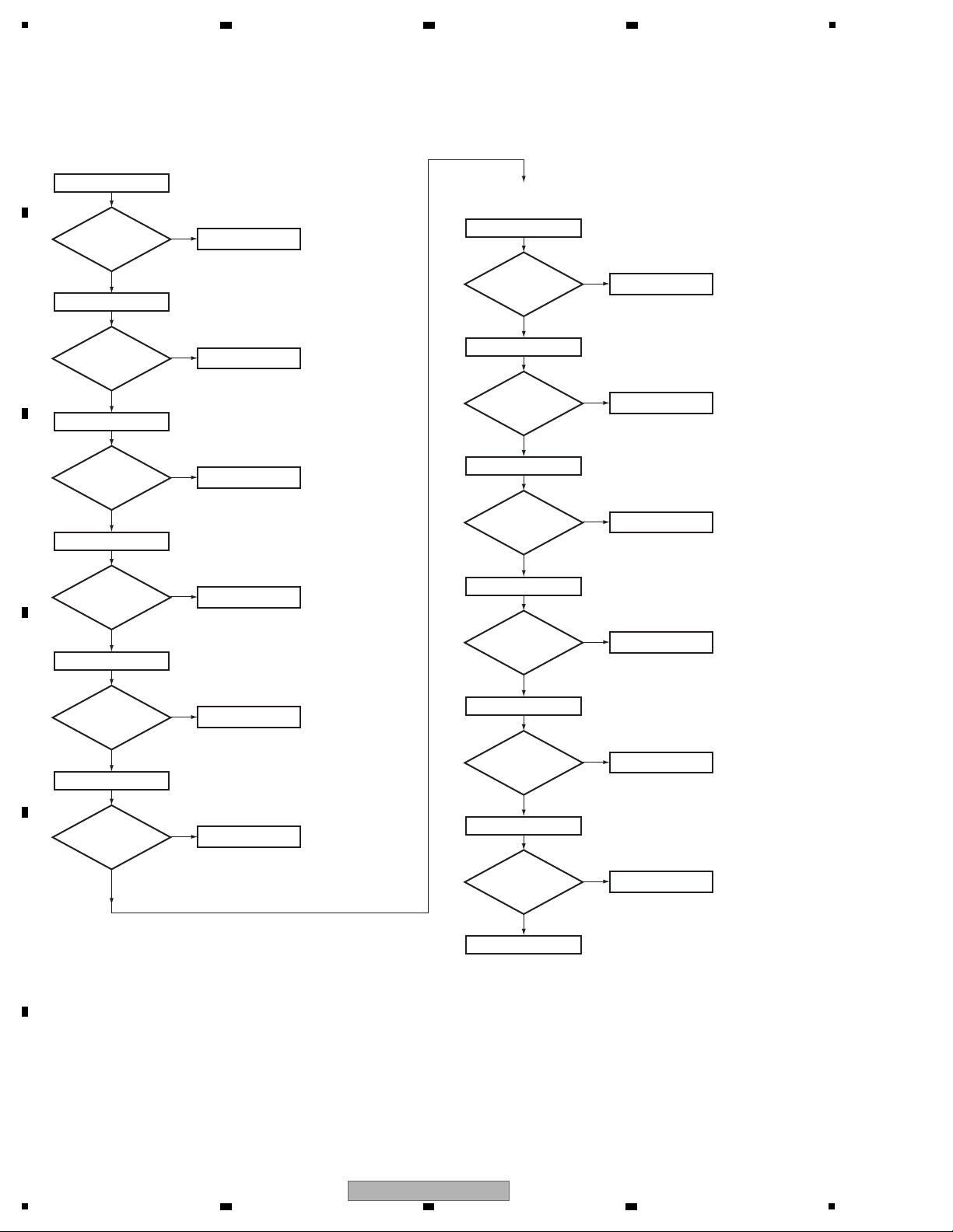
Step 3: Regulator IC
REG101, REG102 (Pin 3)
Is the
voltage of 3.3 V
input?
Replace REG103.
Check the ZD200 2.4 VB
and IC106.
To Step 3
To Step 4
Step 0: Preliminary confirmation
Confirm the following items before checking
Tighten screws securely.
No
Ye s
To Step 1
No
Troubleshooting
[1] DSP TROUBLESHOOTING
Step 2: Regulator IC
Check the REG101,
REG102 and MAIN Assy
Check the REG103 and
MAIN Assy.
REG103 (Pin 3)
Is the
voltage of around
5 V input?
No
Ye s
(to chassis)
ZD200 kathode
Is the
voltage of 2.5 V
output?
No
*The I/O power of DSP Assy is OK
*The IC106 power of DSP Assy
*the DSP IC CORE power of DSP Assy
XMCK
Note: REG101, REG102 is made of
parallel connection.
REG103 (Pin 2)
Is the
voltage of 3.3 V
output?
No
Ye s
Ye s
Ye s
Is the
voltage of 1.2 V
output?
Replace REG101, 102.
Check the path to XTAL101.
No
Ye s
(to chassis)
(to chassis)
REG101, REG102 (Pin 2)
(to chassis)
Step 1: BtoB connector
CP200,CN206,CP105
Are the
connectors securely
inserted?
Turn the power off and
insert the connectors
securely.
No
Ye s
To Step 2
*CN206,CP200 connectors
doesn't connection in case
of DSP JIG B'D use.
BtoB connector
Do screws of COAX
Jack securely tighten?
OR connect GND wire of
DSP JIG B'D to chassis.
Step 4: X'tal
To Step 5
Ye s
IC109 (Pin 6, 7)
No
Is there
a 24.576 MHz
output?
Check the path to pin 6, 7 of IC109.
Replace XTAL101.
Ye s
IC102 (Pin 17)
No
Is there
a 24.576 MHz
input?
5. DIAGNOSIS
5.1 DIAGNOSIS FLOWCHART
6 7 8
A
B
C
D
5
VSX-519V-K
6 7 8
E
F
21
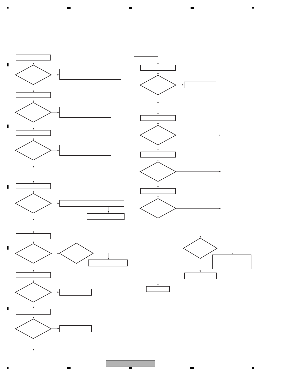
1
Replace IC109.
Ye s
IC109 (Pin 15)
DIR_BCK (Bit clock)
No
Is there
a bit clock
output?
(0 V ⇔ 3.3 V)
Ye s
IC106 (Pin 4)
DAI_MCK (Master clock)
Is there
a master clock
output?
(0 V ⇔ 2.5 V)
Ye s
IC106 (Pin 7)
DAI_LRCK (LR clock)
Is there
a LR clock
output?
(0 V ⇔ 2.5 V)
Ye s
IC106 (Pin 9)
DAI_BCK (Bit clock)
*IC106 Pin1
0 V : DIR
3.3 V : HDMI
Is there
a bit clock
output?
(0 V ⇔ 2.5 V)
Replace IC106.
Check the path
between IC106-pin 1
and MAIN Assy.
No
No
No
No
Is the
voltage of
IC106-pin 1
0 V?
Ye s
Switch
Step 5: DIR
Check the path to pins 10-13
of IC110 or replace IC110.
Check the path to CP105 connector.
Replace IC109.
Check the path to OUTPUT PIN of
JACK105, JACK106.
IC110 (Pins 3, 5)
OPTICAL (Pin3: OPT2, Pin1: OPT1)
Check that the S/PDIF signal is output.
Check that changes by pulling out and inserting the
digital input lines.
Can
observe the
digital signal
?
No
(0 V ⇔ 3.3 V)
Ye s
IC109 (Pin 67)
COAX
Can
observe the
digital signal
?
No
Ye s
Ye s
Check that the data and clock signals are output.
Check that it changes in the Playback and Pause modes of
the USB (iPod).
(0 V ⇔ 3.3 V)
(0 V ⇔ 3.3 V)
(0 V ⇔ 3.3 V)
Ye s
IC109 (Pin 71)
From USB Assy
Can
observe the
digital signal
?
No
(0 V ⇔ 3.3 V)
Check the path to pins 4, 6 of
IC110 or replace IC110.
IC109 (Pins 61, 63)
OPTICAL (Pin61: OPT2, Pin63: OPT1)
Can
observe the
digital signal
?
No
Ye s
(0 V ⇔ 3.3 V)
Check the MAIN Assy.
IC109 (Pin 10)
DIR_MCK (Master clock)
No
No
Ye s
Is there
a master clock
output?
IC109 (Pin 16)
DIR_LRCK (LR clock)
No
Is there
a LR clock
output?
Replace IC109.
(0 V ⇔ 3.3 V)
Ye s
IC109 (Pin 14)
DIR_SDTO (Data)
No
Is there
a data
output?
Is the
voltage of PDN
IC109-pin 31
3.3 V?
Check the USB Assy.
No
To Step 6
A
2 3 4
B
C
D
E
F
22
1
2 3 4
VSX-519V-K
5
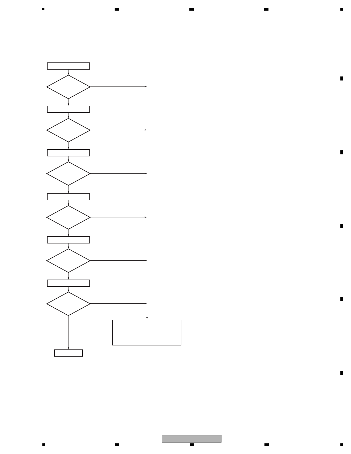
Step 6: DSP output (digital)
Ye s
Digital output of each CH when inputting the digital
signal with audio.
IC109 (Pin 26)
Center/LFE data
No
Is there
a data input?
Ye s
Check the path between IC102
and data & address lines.
SDRAM (IC100), FLASH ROM
(IC101)
IC109 (Pin 25)
Surround back L/R data
No
Is there
a data input?
Ye s
IC109 (Pin 27)
Surround L/R data
No
IIs there
a data input?
Ye s
IC109 (Pin 18)
DSP_BCK (Bit clock)
No
Is there
a bit clock
input?
Ye s
IC109 (Pin 19)
DSP_LRCK (LR clock)
No
Is there
a LR clock
output?
Ye s
IC109 (Pin 28)
Front L/R data
No
Is there
a data input?
(0 V ⇔ 3.3 V)
(0 V ⇔ 3.3 V)
(0 V ⇔ 3.3 V)
(0 V ⇔ 3.3 V)
(0 V ⇔ 3.3 V)
(0 V ⇔ 3.3 V)
To Step 7
6 7 8
A
B
C
D
E
F
VSX-519V-K
5
6 7 8
23
1
Ye s
Replace IC109.
IC109 (Pin 49)
Front R out
No
Is the output
2.5 V fixing?
Replace IC109.
Ye s
Ye s
IC109 (Pin 43)
Surround L out
No
Is the output
2.5 V fixing?
Replace IC109.
IC109 (Pin 41)
Center out
No
Is the output
2.5 V fixing?
Ye s
Replace IC109.
IC109 (Pin 39)
End
LFE out
No
Is the output
2.5 V fixing?
Ye s
Ye s
Replace IC109.
IC109 (Pin 47)
Front L out
No
Is the output
2.5 V fixing?
Replace IC109.
IC109 (Pin 45)
Surround R out
No
Is the output
2.5 V fixing?
Analog output of each CH when inputting the digital
signal (-∞ dB (no signal)).
Replace IC109.
Ye s
IC109 (Pin 43)
Surround L out
No
Is there
a audio signal
output?
Replace IC109.
Ye s
IC109 (Pin 41)
Center out
No
Is there
a audio signal
output?
Replace IC109.
Ye s
IC109 (Pin 39)
LFE out
No
Is there
a audio signal
output?
Step 7: Codec output (analog)
Analog output of each CH when inputting the digital
signal with audio.
Replace IC109.
Ye s
IC109 (Pin 49)
Front R out
No
Is there
a audio signal
output?
Replace IC109.
Ye s
IC109 (Pin 47)
Front L out
No
Is there
a audio signal
output?
Replace IC109.
Ye s
IC109 (Pin 45)
Surround R out
No
Is there
a audio signal
output?
A
2 3 4
B
C
D
E
F
24
1
2 3 4
VSX-519V-K
5
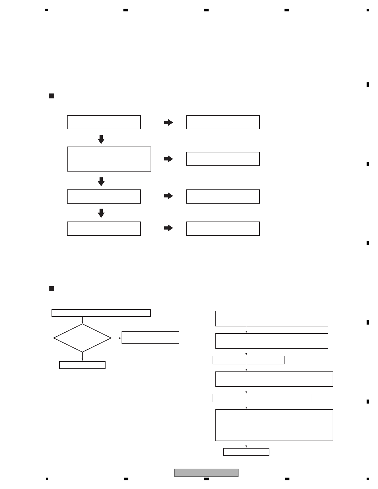
1. Causes for noncompletion of HDMI authentication between the source equipment and this unit
(the HDMI indicator is unlit or flashes)
[2] HDMI TROUBLESHOOTING
Causes for no display or sound from the monitor
HDMI Simple Diagnosis
Replace the HDMI cable.
NG
OK
OK
OK
Connect the source equipment
(player) to the Sink equipment
(monitor) directly.
Replace the Player.
Replace the HDMI cable.
Repare the Receiver.
Repare the Player.
NG
OK
Replace the Monitor.
Repare the Monitor.
NG
POWER ON
Confirm the following items before checking
Do
screws of COAX
jack securely
tighten?
Tighten screws securely.
No
Ye s
Source equipment:
Connect a DVD player to BD, TV or DVR.
To Step 2
To Step 1
Sink equipment:
Connect a TV to HDMI OUT.
Turn on the power of the Receiver and equipments
which was connected with HDMI.
Function switch (BD, TV or DVR)
Switch the function that HDMI was assigned.
Factory shipments setting:
HDMI 1: BD/DVD
HDMI 2: TV/SAT
HDMI 3: DVR/VCR
HDMI Troubleshooting
Step 0: Preliminary confirmation
Step 1: Connect the HDMI equipment
6 7 8
A
B
C
D
5
VSX-519V-K
6 7 8
E
F
25
1
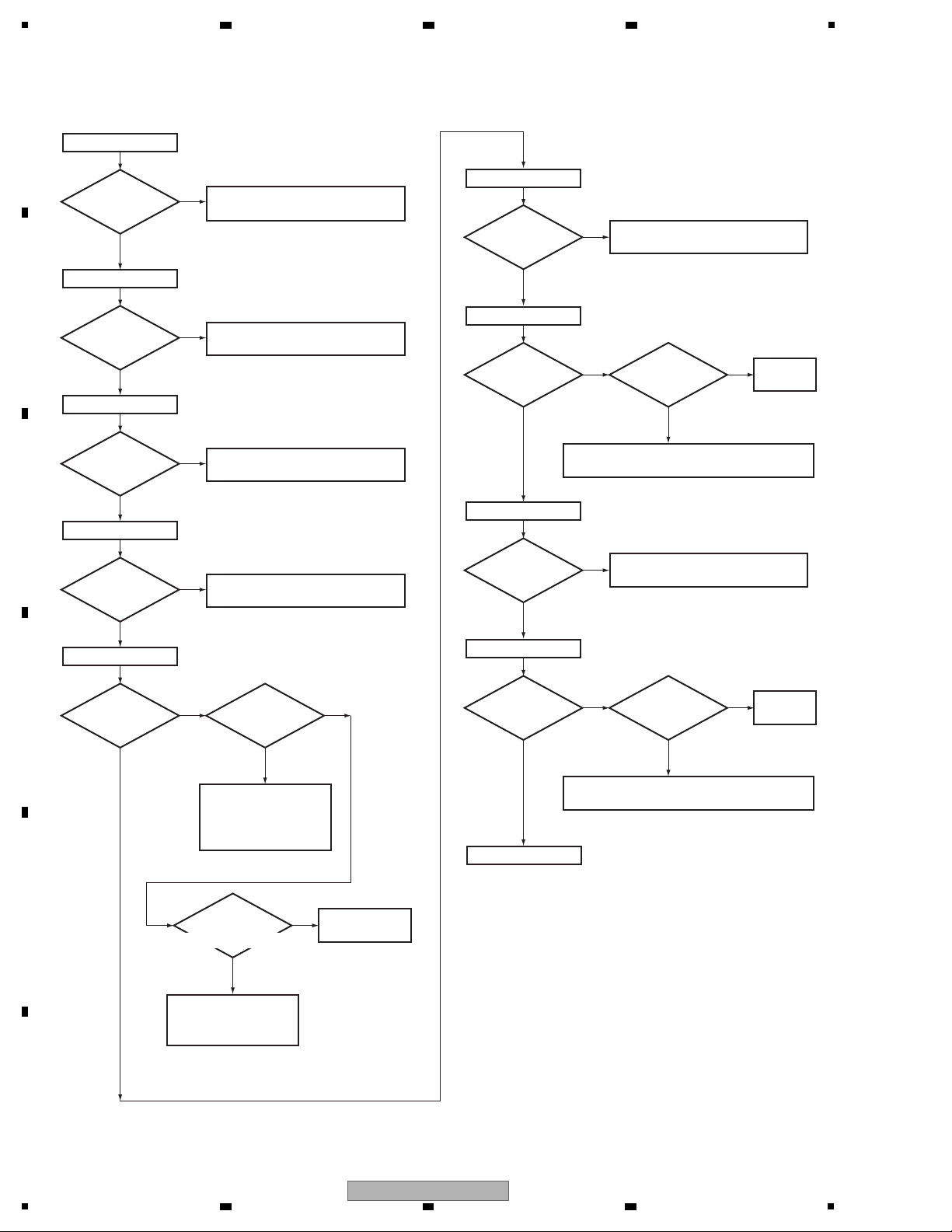
CN1002 (Pin 10)
Is the voltage
0 to 3.3 V?
No
SUB_ON
Diagnose the MAIN Assy.
Diagnose the MAIN Assy.
Diagnose the MAIN Assy.
Diagnose the MAIN Assy.
Ye s
CN1002 (Pins 1, 2)
Is the voltage
3.3 V?
Is the voltage
3.3 V?
Is the voltage
3.3 V?
Is the voltage
5 V?
No
SUB MICOM 3.3V
Q1204 (collector)
No
SUB MICOM 3.3V
Ye s
Ye s
CN1001 (Pin 3)
No
HDMI_5V
Ye s
CN1001 (Pins 1, 2)
No
HDMI_3.3V
Ye s
Is Q1204
base voltage
2.6 V?
No
Ye s
To Step 3
Is the voltage
3.3 V?
Is the voltage
1.8 V?
Is the voltage
3.3 V?
Is the voltage
1.2 V?
replace
IC1005
replace
IC1004
IC1005 (Pin 3)
No
HDMI 3.3V
Ye s
IC1005 (Pin 2)
No
HDMI 1.8V
Ye s
Check the parts and patterns in
the path.
Check the parts and patterns in
the path.
Is IC1005
abnormally
hot?
Is IC1004
abnormally
hot?
No
Ye s
IC1004 (Pin 3)
No
HDMI 3.3V
HDMI 1.2V
Ye s
The output and GND may be short-circuited.
Check the path between them.
Check the parts and
patterns in the path.
Replace Q1204,
IC1003, etc.
Check the parts and
patterns in the path
Q1405, Q1204, etc.
The output and GND may be short-circuited.
Check the path between them.
IC1004 (Pin 2)
No
Ye s
No
Ye s
Step 2: Power supply
replace Q1405
No
Ye s
Is Q1405
collector voltage
0 V? (base is 3.3 V)
A
2 3 4
B
C
D
E
F
26
1
VSX-519V-K
2 3 4
5
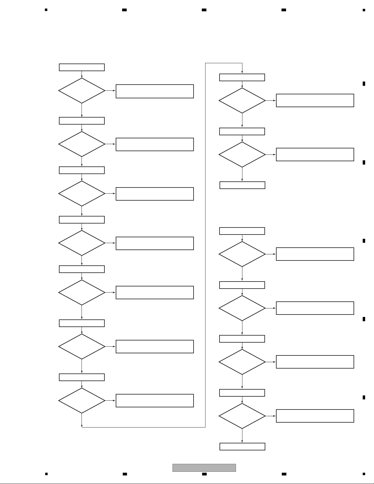
To Step 5
Step 4: X'TAL
Replace IC1003 or X1401.
Replace IC1001 or X1001.
Is there
a 12 MHz
output?
Is there
a 12 MHz
output?
Is there
a 27 MHz
output?
Is there
a 27 MHz
output?
IC1003 (Pin 15)
No
Ye s
IC1003 (Pin 13)
No
Ye s
Check the path to pin13 of IC1003.
Replace IC1003.
IC1001 (Pin 5)
No
Ye s
IC1001 (Pin 4)
No
Ye s
Check the path to pin4 of IC1001.
Replace IC1001.
To Step 4
Check the parts and patterns in
the path pin 87 of IC1003.
Is the voltage
0 to 3.3 V?
Is there a data
0 to 3.3 V?
IC1001 (Pin 21)
No
HR_RST
Ye s
IC1002 (Pin 25)
No
Ye s
Check the parts and patterns in
the path pin 89 of IC1003.
Step 3: Diagnosis
CN1002 (Pin 6)
Is the voltage
0 to 3.3 V?
No
CE
Diagnose the MAIN Assy.
Diagnose the MAIN Assy.
Diagnose the MAIN Assy.
Diagnose the MAIN Assy.
Diagnose the MAIN Assy.
Ye s
CN1002 (Pin 7)
Is the voltage
0 to 3.3 V?
No
SUB_PDN
CN1002 (Pin 3)
Is there
a data input?
(0 to 3.3 V)
Is there
a data input?
(0 to 3.3 V)
No
CSCK_MAIN
Ye s
Ye s
CN1002 (Pin 8)
Is there
a data input?
(0 to 3.3 V)
No
MAIN_IRQ
Ye s
CN1002 (Pin 9)
Is there
a data output?
(0 to 3.3 V)
Is there
a data output?
(0 to 3.3 V)
No
SUB_IRQ
Check the parts and patterns in
the path IC1003.
Ye s
CN1002 (Pin 4)
No
SCDO_MAIN
Ye s
CN1002 (Pin 5)
No
SCDI_MAIN
Ye s
Check the parts and patterns in
the path IC1003.
Each data lines confirmation checks it after standby OFF/ON.
6 7 8
A
B
C
D
5
VSX-519V-K
6 7 8
E
F
27
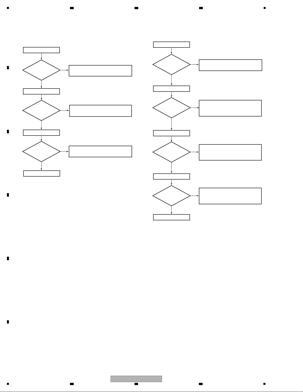
1
JACK1004 (Pin 19)
HPD_SINK
Check the JACK1004. If JACK
1004 is failure, replace JACK1004.
Ye s
JACK1003 (Pin 19)
HPD3
Ye s
No
No
Check the JACK1002 and IC1001.
If JACK1002 or IC1001 is failure,
replace JACK1002 or IC1001.
JACK1002 (Pin 19)
No
HPD2
Check the JACK1003 and IC1001.
If JACK1003 or IC1001 is failure,
replace JACK1003 or IC1001.
Ye s
JACK1001 (Pin 19)
HPD1
* When connected the equipment to IN2 (TV/SAT);
* When connected the equipment to IN1 (BD/DVD);
* When connected the equipment to IN3 (DVR/VCR)
Is the
voltage 5 V
when selecting
IN2?
Is the
voltage 5 V
when selecting
IN3?
JACK1003 (Pin 18)
+5V_R3
Is the voltage
5 V?
Is the voltage
5 V?
Is the voltage
5 V?
Is the voltage
5 V?
Check the JACK1003. If JACK
1003 is failure, replace JACK1003.
Check the JACK1001. If JACK
1001 is failure, replace JACK1001.
Check the JACK1002. If JACK
1002 is failure, replace JACK1002.
Ye s
JACK1002 (Pin 18)
+5V_R2
Ye s
No
No
JACK1001 (Pin 18)
No
+5V_R1
Ye s
* When connected the equipment to IN1(BD/DVD);
Check the JACK1001 and IC1001.
If JACK1001 or IC1001 is failure,
replace JACK1001 or IC1001.
No
Ye s
Is the
voltage 5 V
when selecting
IN1?
To Step 7
To Step 6
Step 5: IN/OUTPUT Diagnosis
Step 6: Hot plug detect
A
2 3 4
B
C
D
E
F
28
1
2 3 4
VSX-519V-K
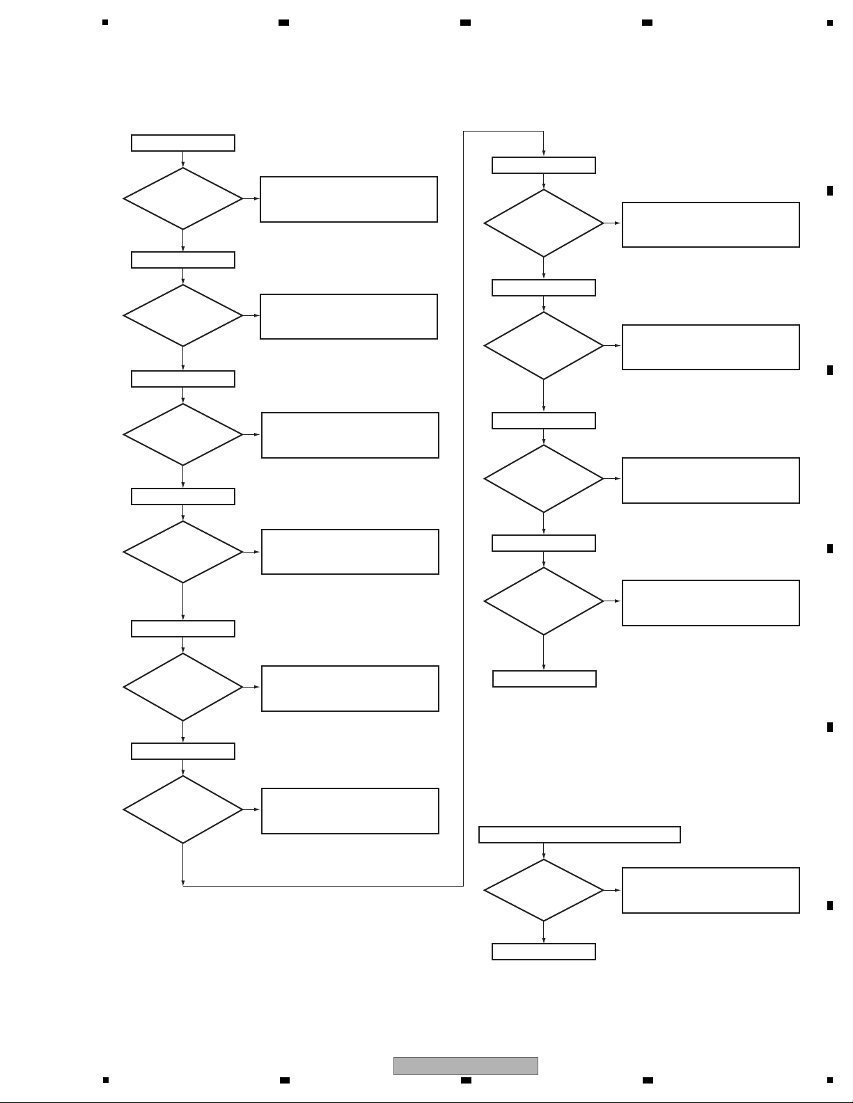
IC1002 (Pins 30,31,33,34,36,37,39,40)
TMDS OUTPUT
SDA (HDMI IN2 (TV/SAT))
No
IC1001 (Pin 40)
Is
there a same
signal as IC1002-pin 49
when selecting
IN2?
Ye s
Check the IC1001 and JACK1002.
If IC1001 or JACK1002 is failure,
replace IC1001 or JACK1002.
* When connected the equipment to IN2 (TV/SAT):
SCL (HDMI IN2 (TV/SAT))
No
IC1001 (Pin 39)
Is
there a same
signal as IC1002-pin 48
when selecting
IN2?
Ye s
Check the IC1001 and JACK1002.
If IC1001 or JACK1002 is failure,
replace IC1001 or JACK1002.
Check the IC1001 or IC1002.
If IC1001 or IC1002 is failure,
replace IC1001 or IC1002.
(0 to 5 V)
(0 to 5 V)
End
No
Are there
signals(approx. 0.5
Vp-p) in all
lines?
Ye s
Step 8: TMDS
SDA (HDMI IN3 (DVR/VCR))
No
IC1001 (Pin 36)
Is
there a same
signal as IC1002-pin 49
when selecting
IN3?
Ye s
Check the IC1001 and JACK1001.
If IC1001 or JACK1001 is failure,
replace IC1001 or JACK1001.
* When connected the equipment to IN3 (DVR/VCR):
SCL (HDMI IN3 (DVR/VCR))
No
IC1001 (Pin 35)
Is
there a same
signal as IC1002-pin 48
when selecting
IN3?
Ye s
Check the IC1001 and JACK1001.
If IC1001 or JACK1001 is failure,
replace IC1001 or JACK1001.
(0 to 5 V)
(0 to 5 V)
To Step 8
IC1002 (Pin 47)
SDA (HDMI OUT)
SDA (HDMI IN1(BD/DVD))
Does
a signal output in
constant period
(0 to 5 V)
?
Check the JACK1004 and IC1002.
If JACK1004 or IC1002 is failure,
replace JACK1004 or IC1002.
No
No
No
Ye s
IC1002 (Pin 46)
SCL (HDMI OUT)
Does
a clock output in
constant period
(0 to 5 V)
?
Check the JACK1004 and IC1002.
If JACK1004 or IC1002 is failure,
replace JACK1004 or IC1002.
Ye s
IC1001 (Pin 44)
Is
there a same
signal as IC1002-pin 49
when selecting
IN1?
Ye s
Check the IC1001 and JACK1003.
If IC1001 or JACK1003 is failure,
replace IC1001 or JACK1003.
* When connected the equipment to IN1(BD/DVD);
SCL (HDMI IN1(BD/DVD))
No
IC1001 (Pin 43)
Is
there a same
signal as IC1002-pin 48
when selecting
IN1?
Ye s
Check the IC1001 and JACK1003.
If IC1001 or JACK1003 is failure,
replace IC1001 or JACK1003.
SDA_SINK
No
No
SCL_SINK
IC1002 (Pin 49)
Is
there a same
signal as IC1001-pin 24
(0 to 3.3V)
?
Ye s
Check the IC1002 and IC1001.
If IC1002 or IC1001 is failure,
replace IC1002 or IC1001.
Check the IC1002 and IC1001.
If IC1002 or IC1001 is failure,
replace IC1002 or IC1001.
IC1002 (Pin 48)
Is
there a same
signal as IC1001-pin 23
(0 to 3.3V)
?
Ye s
(0 to 5 V)
(0 to 5 V)
Step 7: SDA /SCL
5
6 7 8
A
B
C
D
5
VSX-519V-K
6 7 8
E
F
29
 Loading...