

Page 1
PIONEER CORPORATION 1-1, Shin-ogura, Saiwai-ku, Kawasaki-shi, Kanagawa 212-0031, Japan
PIONEER ELECTRONICS (USA) INC. P.O. Box 1760, Long Beach, CA 90801-1760, U.S.A.
PIONEER EUROPE NV Haven 1087, Keetberglaan 1, 9120 Melsele, Belgium
PIONEER ELECTRONICS ASIACENTRE PTE. LTD. 253 Alexandra Road, #04-01, Singapore 159936
PIONEER CORPORATION
2012
ADVANCED
MCACC
FL OFF
iPod iPhone iPadHDMI
AV RECEIVER
SC-68
SC-67
INPUT
SELECTOR
STANDBY/ON
MASTER
VOLUME
ORDER NO.
RRV4325
SC-68
THIS MANUAL IS APPLICABLE TO THE FOLLOWING MODEL(S) AND TYPE(S).
Model Type Power Requirement Remarks
SC-68 UXJCB AC 120V
SC-67 UXJCB AC 120V
K-FZV JULY
2012 Printed in Japan
Page 2
1
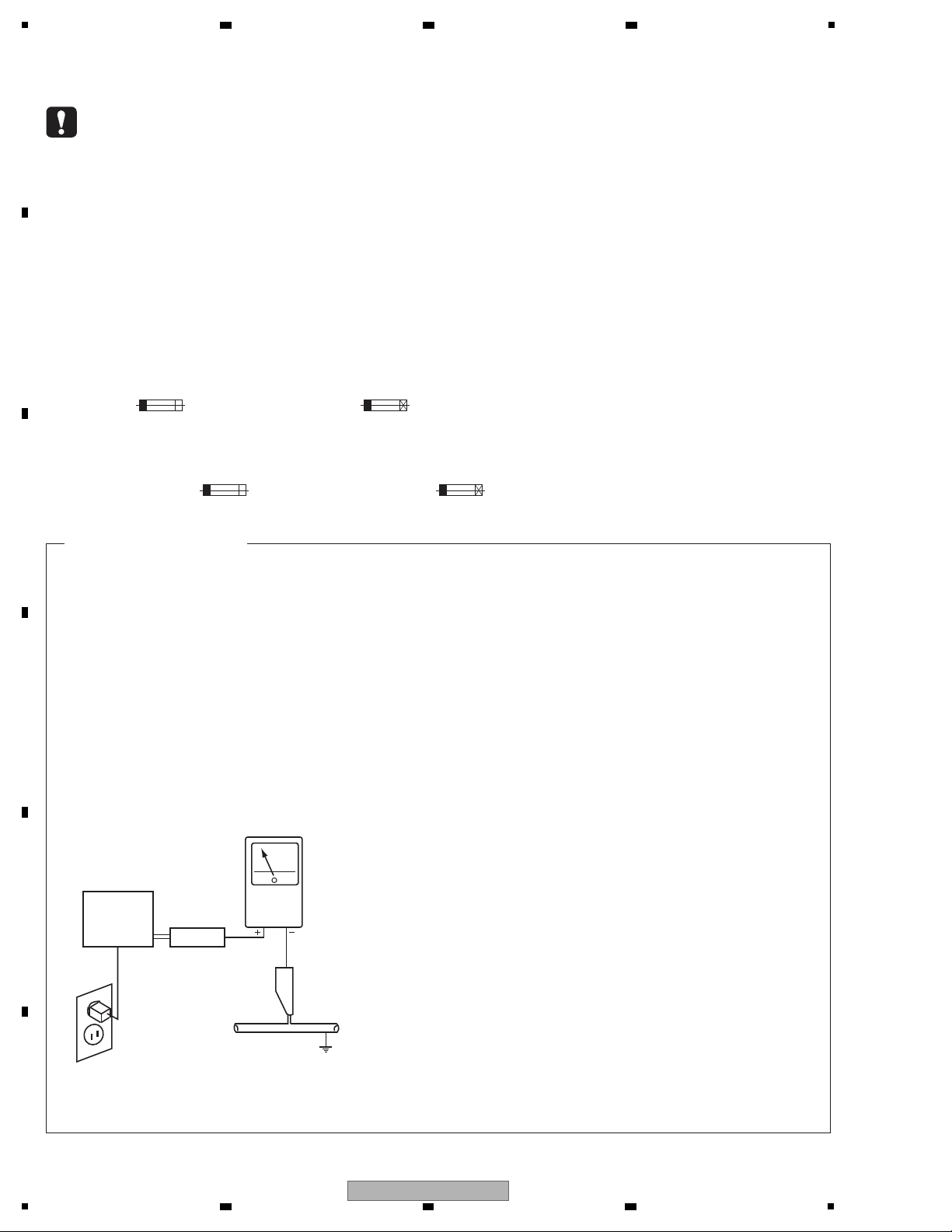
1. SAFETY PRECAUTIONS
The following check should be performed for the
continued protection of the customer and service
technician.
LEAKAGE CURRENT CHECK
Measure leakage current to a known earth ground
(water pipe, conduit, etc.) by connecting a leakage
current tester such as Simpson Model 229-2 or
equivalent between the earth ground and all exposed
metal parts of the appliance (input/output terminals,
screwheads, metal overlays, control shaft, etc.). Plug
the AC line cord of the appliance directly into a 120V
AC 60 Hz outlet and turn the AC power switch on. Any
current measured must not exceed 0.5 mA.
ANY MEASUREMENTS NOT WITHIN THE LIMITS
OUTLINED ABOVE ARE INDICATIVE OF A POTENTIAL
SHOCK HAZARD AND MUST BE CORRECTED BEFORE
RETURNING THE APPLIANCE TO THE CUSTOMER.
2. PRODUCT SAFETY NOTICE
Many electrical and mechanical parts in the appliance
have special safety related characteristics. These are
often not evident from visual inspection nor the protection
afforded by them necessarily can be obtained by using
replacement components rated for voltage, wattage, etc.
Replacement parts which have these special safety
characteristics are identified in this Service Manual.
Electrical components having such features are
identified by marking with a > on the schematics and on
the parts list in this Ser
vice Manual.
The use of a substitute replacement component which
does not have the same safety characteristics as the
PIONEER recommended replacement one, shown in the
parts list in this Service Manual, may create shock, fire,
or other hazards.
Product Safety is continuously under review and new
instructions are issued from time to time. For the latest
information, always consult the current PIONEER Service
Manual. A subscription to, or additional copies of,
PIONEER Service Manual may be obtained at a nominal
charge from PIONEER.
Leakage
current
tester
Reading should
not be above
0.5 mA
Device
under
test
Test all
exposed metal
surfaces
Also test with
plug reversed
(Using AC adapter
plug as required)
Earth
ground
AC Leakage Test
(FOR USA MODEL ONLY)
WARNING
This product contains lead in solder and certain electrical parts contain chemicals which are known to the state of California to
cause cancer, birth defects or other reproductive harm.
56 noitisoporP - 6.94252 noitceS edoC ytefaS & htlaeH
NOTICE
(FOR CANADIAN MODEL ONLY)
Fuse symbols (fast operating fuse) and/or (slow operating fuse) on PCB indicate that replacement parts must
be of identical designation.
REMARQUE
(POUR MODÈLE CANADIEN SEULEMENT)
Les symboles de fusible (fusible de type rapide) et/ou (fusible de type lent) sur CCI indiquent que les pièces
de remplacement doivent avoir la même désignation.
This service manual is intended for qualified service technicians ; it is not meant for the casual do-it-
yourselfer. Qualified technicians have the necessary test equipment and tools, and have been trained
to properly and safely repair complex products such as those covered by this manual.
Improperly performed repairs can adversely affect the safety and reliability of the product and may
void the warranty. If you are not qualified to perform the repair of this product properly and safely, you
should not risk trying to do so and refer the repair to a qualified service technician.
2 3 4
SAFETY INFORMATION
A
B
C
D
E
F
2
1
2 3 4
SC-68
Page 3

5
6 7 8
CONTENTS
SAFETY INFORMATION.......................................................................................................................................................... 2
1. SERVICE PRECAUTIONS.................................................................................................................................................... 5
1.1 NOTES ON SOLDERING...............................................................................................................................................5
1.2 NOTES ON REPLACING ...............................................................................................................................................5
1.3 CAUTION........................................................................................................................................................................ 5
1.4 NOTES ON ASSEMBLING.............................................................................................................................................6
2. SPECIFICATIONS................................................................................................................................................................. 7
3. BASIC ITEMS FOR SERVICE ............................................................................................................................................10
3.1 CHECK POINTS AFTER SERVICING ......................................................................................................................... 10
3.2 PCB LOCATIONS ......................................................................................................................................................... 11
3.3 JIGS LIST .....................................................................................................................................................................13
4. BLOCK DIAGRAM .............................................................................................................................................................. 14
4.1 OVERALL WIRING DIAGRAM ..................................................................................................................................... 14
4.2 BLOCK DIAGRAM FOR AUDIO BLOCK......................................................................................................................16
4.3 BLOCK DIAGRAM FOR DIGITAL MAIN VIDEO BLOCK .............................................................................................20
4.4 BLOCK DIAGRAM FOR DIGITAL MAIN AUDIO BLOCK .............................................................................................22
4.5 BLOCK DIAGRAM FOR COMPOSITE VIDEO BLOCK ............................................................................................... 24
4.6 BLOCK DIAGRAM FOR COMPONENT VIDEO BLOCK..............................................................................................25
4.7 BLOCK DIAGRAM FOR POWER BLOCK (1) ..............................................................................................................26
4.8 BLOCK DIAGRAM FOR POWER BLOCK (2) ..............................................................................................................28
5. DIAGNOSIS ........................................................................................................................................................................30
5.1 DIAGNOSIS FLOWCHART .......................................................................................................................................... 30
5.2 CIRCUIT DESCRIPTION..............................................................................................................................................39
6. SERVICE MODE................................................................................................................................................................. 48
6.1 TEST MODE.................................................................................................................................................................48
7. DISASSEMBLY ...................................................................................................................................................................50
8. EACH SETTING AND ADJUSTMENT................................................................................................................................70
8.1 ADJUSTMENT REQUIRED WHEN THE UNIT IS REPAIRED OR REPLACED..........................................................70
8.2 HOW TO SAVE AND LOAD THE SETTING USING BACKUP FUNCTION WITH USB MEMORY.............................. 71
8.3 REGION WRITING.......................................................................................................................................................72
8.4 HOW TO UPDATE FIRMWARE.................................................................................................................................... 73
9. EXPLODED VIEWS AND PARTS LIST...............................................................................................................................76
9.1 PACKING SECTION .....................................................................................................................................................76
9.2 EXTERIOR SECTION .................................................................................................................................................. 78
9.3 REAR SECTION...........................................................................................................................................................80
9.4 CHASSIS SECTION.....................................................................................................................................................82
9.5 FRONT SECTION ........................................................................................................................................................84
10. SCHEMATIC DIAGRAM.................................................................................................................................................... 86
10.1 AUDIO ASSY (1/3) (GUIDE PAGE) ............................................................................................................................ 86
10.2 AUDIO ASSY (2/3)......................................................................................................................................................92
10.3 AUDIO ASSY (3/3)......................................................................................................................................................94
10.4 DAC HIGH ASSY (1/2) ...............................................................................................................................................96
10.5 DAC HIGH ASSY (2/2) ...............................................................................................................................................98
10.6 FRONT HDMI USB ASSY ........................................................................................................................................100
10.7 USB RECT ASSY and MULTI CH IN ASSY (SC-68)................................................................................................ 102
10.8 USB DAC ASSY (SC-68).......................................................................................................................................... 104
10.9 DIGITAL MAIN ASSY (1/11) ..................................................................................................................................... 106
10.10 DIGITAL MAIN ASSY (2/11) ................................................................................................................................... 108
10.11 DIGITAL MAIN ASSY (3/11) ................................................................................................................................... 110
10.12 DIGITAL MAIN ASSY (4/11) ................................................................................................................................... 112
10.13 DIGITAL MAIN ASSY (5/11) ................................................................................................................................... 114
10.14 DIGITAL MAIN ASSY (6/11) ..................................................................................................
10.15 DIGITAL MAIN ASSY (7/11) ................................................................................................................................... 118
10.16 DIGITAL MAIN ASSY (8/11) ................................................................................................................................... 120
10.17 DIGITAL MAIN ASSY (9/11) ................................................................................................................................... 122
10.18 DIGITAL MAIN ASSY (10/11) ................................................................................................................................. 124
10.19 DIGITAL MAIN ASSY (11/11) ................................................................................................................................. 126
10.20 INTERFACE ASSY .................................................................................................................................................128
10.21 COMPONENT ASSY (1/2) ..................................................................................................................................... 130
10.22 COMPONENT ASSY (2/2) ..................................................................................................................................... 132
10.23 COMPOSITE ASSY................................................................................................................................................134
10.24 MIC HP ASSY.........................................................................................................................................................136
10.25 DISPLAY ASSY (1/2) ..............................................................................................................................................138
10.26 DISPLAY ASSY (2/2) ..............................................................................................................................................140
10.27 VOL ASSY and POWER SW ASSY ....................................................................................................................... 142
SC-68
5
6 7 8
.................................116
A
B
C
D
E
F
3
Page 4

1
2 3 4
10.28 ENCODER ASSY....................................................................................................................................................143
10.29 IR INTERFACE_M ASSY and BUFFER GND ASSY..............................................................................................144
10.30 IR BUFFER ASSY...................................................................................................................................................146
10.31 D AMP ASSY (1/7)..................................................................................................................................................148
A
10.32 D AMP ASSY (2/7)..................................................................................................................................................150
10.33 D AMP ASSY (3/7)..................................................................................................................................................152
10.34 D AMP ASSY (4/7)..................................................................................................................................................154
10.35 D AMP ASSY (5/7)..................................................................................................................................................156
10.36 D AMP ASSY (6/7)..................................................................................................................................................158
10.37 D AMP ASSY (7/7)..................................................................................................................................................160
10.38 PRIMARY ASSY .....................................................................................................................................................162
10.39 PRIMARY SHIELD ASSY (SC-67) and REG ASSY ...............................................................................................164
10.40 IR REG ASSY .........................................................................................................................................................166
10.41 B DIODE ASSY.......................................................................................................................................................168
10.42 CONNECT ASSY....................................................................................................................................................169
B
10.43 FB-CONNECT ASSY..............................................................................................................................................170
10.44 PRE BRIDGE ASSY ...............................................................................................................................................171
10.45 A-DAC BRIDGE ASSY............................................................................................................................................172
10.46 D-AUDIO BRIDGE ASSY........................................................................................................................................173
10.47 D-DAC BRIDGE ASSY............................................................................................................................................174
10.48 FRONT BRIDGE ASSY ..........................................................................................................................................175
10.49 DISPLAY BRIDGE ASSY ........................................................................................................................................176
10.50 F-IN BRIDGE ASSY................................................................................................................................................177
10.51 MCH BRIDGE ASSY (SC-68).................................................................................................................................178
10.52 A REG BRIDGE ASSY............................................................................................................................................179
10.53 MIC HP GUARD, FAN CONNECT, BIND DM CABLE and BIND B CABLE ASSYS...............................................180
10.54 FFC GUARD, VREG GUARD and PANEL GUARD ASSYS ...................................................................................181
11. PCB CONNECTION DIAGRAM ......................................................................................................................................182
C
11.1 AUDIO ASSY ............................................................................................................................................................182
11.2 DAC HIGH ASSY ......................................................................................................................................................186
11.3 FRONT HDMI USB ASSY.........................................................................................................................................190
11.4 USB RECT ASSY .....................................................................................................................................................191
11.5 MULTI CH IN ASSY (SC-68).....................................................................................................................................192
11.6 USB DAC ASSY (SC-68) ..........................................................................................................................................194
11.7 DIGITAL MAIN ASSY ................................................................................................................................................198
11.8 INTERFACE ASSY....................................................................................................................................................202
11.9 COMPONENT ASSY ................................................................................................................................................204
11.10 COMPOSITE ASSY................................................................................................................................................208
11.11 MIC HP ASSY.........................................................................................................................................................210
D
11.12 DISPLAY ASSY.......................................................................................................................................................212
11.13 VOL ASSY, POWER SW ASSY and ENCODER ASSY..........................................................................................216
11.14 IR BUFFER ASSY...................................................................................................................................................218
11.15 BUFFER GND ASSY and IR INTERFACE_M ASSY ..............................................................................................222
11.16 D AMP ASSY ..........................................................................................................................................................224
11.17 PRIMARY ASSY and PRIMARY SHIELD ASSY (SC-67) .......................................................................................228
11.18 REG ASSY..............................................................................................................................................................232
11.19 IR REG ASSY and B DIODE ASSY........................................................................................................................234
11.20 CONNECT ASSY and FB-CONNECT ASSY..........................................................................................................238
11.21 PRE BRIDGE, A-DAC BRIDGE, D-AUDIO BRIDGE and D-DAC BRIDGE ASSYS................................................240
11.22 FRONT BRIDGE ASSY and DISPLAY BRIDGE ASSY ..........................................................................................244
E
11.23 F-IN BRIDGE ASSY................................................................................................................................................246
11.24 MCH BRIDGE ASSY (SC-68).......................................................................................................
..........................248
11.25 A REG BRIDGE ASSY............................................................................................................................................249
11.26 MIC HP GUARD ASSY and FAN CONNECT ASSY...............................................................................................250
11.27 BIND DM CABLE, BIND B CABLE, FFC GUARD and VREG GUARD ASSYS......................................................254
12. PCB PARTS LIST ............................................................................................................................................................256
F
4
1
2 3 4
SC-68
Page 5
5
• For environmental protection, lead-free solder is used on the printed circuit boards mounted in this unit.
Be sure to use lead-free solder and a soldering iron that can meet specifications for use with lead-free solders for repairs
accompanied by reworking of soldering.
• Compared with conventional eutectic solders, lead-free solders have higher melting points, by approximately 40 °C.
Therefore, for lead-free soldering, the tip temperature of a soldering iron must be set to around 373 °C in general, although
the temperature depends on the heat capacity of the PC board on which reworking is required and the weight of the tip of
the soldering iron.
Do NOT use a soldering iron whose tip temperature cannot be controlled.
Compared with eutectic solders, lead-free solders have higher bond strengths but slower wetting times and higher melting
temperatures (hard to melt/easy to harden).
The following lead-free solders are availab
le as service parts:
• Parts numbers of lead-free solder:
GYP1006 1.0 in dia.
GYP1007 0.6 in dia.
GYP1008 0.3 in dia.
The part listed below is difficult to replace as a discrete component part.
When the part listed in the table is defective, replace whole Assy.
Parts that is Difficult to Replace
ASSY NAME
PCB ASSY
Part No.
Ref No. FUNCTION Part No. Remarks
IC903 HDMI RECEIVER ------------------- IC with heat-pad
IC1204 DIGITAL VIDEO FORMAT
CONVERTER
-------------------
BGA
IC1212 DDR2-SDRAM ------------------- BGA
IC1602 HDMI TRANSMITTER ------------------- IC with heat-pad
IC1609 HDMI TRANSMITTER ------------------- IC with heat-pad
IC9002 1st DSP ------------------- IC with heat-pad
IC9203 LAN PHY ------------------- IC with heat-pad
IC9204 MEDIA PROCESSOR ------------------- BGA
IC9510 REGULATOR ------------------- IC with heat-pad
IC9520 REGULATOR ------------------- IC with heat-pad
IC9521 REGULATOR ------------------- IC with heat-pad
IC9522 REGULATOR ------------------- IC with heat-pad
IC9524 REGULATOR ------------------- IC with heat-pad
IC9602 HDMI RECEIVER
HI-PASS FILTER
HI-PASS FILTER
------------------- IC with heat-pad
DIGITAL MAIN
ASSY
AWX9904
(SC-68)
AWX1198
(SC-67)
IC9702
C9577
C9578
2nd DSP ------------------- IC with heat-pad
------------------- IC with heat-pad
------------------- IC with heat-pad
D AMP ASSY
AWX1214
(SC-68)
AWX1218
(SC-67)
Q4101,4102
Q4201,4202
Q4301,4302
Q4401,4402
Q4501,4502
Q4601,4602
Q4701,4702
Q4801,4802
Q4901,4902
FET ------------------- Land is under parts
• Discharging
Before starting the diagnosis, wait for three minutes until the electricity of the unit is discharged.
• Ground Points
Please refer to “Ground Points”.
6 7 8
1. SERVICE PRECAUTIONS
1.1 NOTES ON SOLDERING
1.2 NOTES ON REPLACING
A
B
1.3 CAUTION
5
6 7 8
SC-68
C
D
E
F
5
Page 6
1
IR BUFFER ASSY
Accessory of Panel Base
IR Cover 85
D AMP ASSY
Rear Panel
BUFFER GND ASSY
BIND DM CABLE ASSY
Note : The right and left positions for the attachment positioning of digital amplifier block are gradual, however, adjust the
front and back positions correctly. For the positioning procedure, refer to "7. DISASSEMBLY".
When assembling the digital amplifier block, please note the following points of screws to prevent from short-circuit.
The following 7 points of screws must always be used AMZ30P060FTC
Points to be watched for swarf
If a screw at any of these points needs to be removed for service,
be sure to check that the swarf is not on the screw before refastening.
2 3 4
1.4 NOTES ON ASSEMBLING
A
B
C
D
E
F
6
1
2 3 4
SC-68
Page 7

5
Amplifier section
Continuous average power output*
8 Ω ................................................................................................................................. 140 W** per channel
6 Ω ..................................................................................... 190 W (SC-68)*** / 180 W (SC-67)*** per channel
* Measured pursuant to the Federal Trade Commission’s Trade Regulation rule on Power Output Claims for
Amplifiers
** 1 kHz with no more than 0.08 %**** total harmonic distortion
*** 1 kHz with no more than 1 %**** total harmonic distortion
**** Measured by Audio Spectrum Analyzer
Multi channel simultaneous power output (1 kHz, 1 %, 8 Ω)
9 ch total.......................................................................................................... 810 W (SC-68)/770 W (SC-67)
Continuous Power Output (1 kHz, 8 Ω, 0.08 %)
Front ..................................................................................................................................... 140 W + 140 W
Center .................................................................................................................................... 140 W
Surround ............................................................................................................................... 140 W + 140 W
Surround back ....................................................................................................................... 140 W + 140 W
Front height/Front wide .......................................................................................................... 140 W + 140 W
Continuous Power Output (1 kHz, 6 Ω, 1.0 %)
In case of SC-68
Front ...................................................................................................................................... 190 W + 190 W
Center..................................................................................................................................... 190 W
Surround ................................................................................................................................ 190 W + 190 W
Surround back ........................................................................................................................ 190 W + 190 W
Front height/Front wide........................................................................................................... 190 W + 190 W
In case of SC-67
Front....................................................................................................................................... 180 W + 180 W
Center..................................................................................................................................... 180 W
Surround................................................................................................................................. 180 W + 180 W
Surround back
........................................................................................................................ 180 W + 180 W
Front height/Front wide........................................................................................................... 180 W + 180 W
Continuous Power Output (1 kHz, 4 Ω, 1.0 %)
In case of SC-68
Front....................................................................................................................................... 250 W + 250 W
Center..................................................................................................................................... 250 W
Surround ................................................................................................................................ 250 W + 250 W
Surround back ....................................................................................................................... 250 W + 250 W
Front height/Front wide........................................................................................................... 250 W + 250 W
In case of SC-67
Front ...................................................................................................................................... 230 W + 230 W
Center .................................................................................................................................... 230 W
Surround ............................................................................................................................... 230 W + 230 W
Surround back ....................................................................................................................... 230 W + 230 W
Front height/Front wide .......................................................................................................... 230 W + 230 W
Total harmonic distortion .............................................................................. 0.04 % (1 kHz, 130 W + 130 W, 8 Ω )
Guaranteed speaker impedance........................................................................................................... 4 Ω to 16 Ω
Audio Section
Input (Sensitivity/Impedance)
PHONO MM ............................................................................................................................... 5 mV/47 k Ω
LINE ........................................................................................................................................ 400 mV/47 k Ω
Output (Level/Impedance)
REC........................................................................................................................................400 mV/2.2 k Ω
Signal-to-Noise Ratio (IHF, short circuited, A network)
LINE .................................................................................................................................................... 103 dB
Tuner Section
Frequency Range (FM)......................................................................................................... 87.5 MHz to 108 MHz
Antenna Input (FM) .................................................................................................................... 75 Ω unbalanced
Frequency Range (AM)...........................................................................................................530 kHz to 1700 kHz
Antenna (AM) ................................................................................................................. Loop antenna (balanced)
6 7 8
2. SPECIFICATIONS
SC-68
5
6 7 8
A
B
C
D
E
F
7
Page 8

1
Video Section
Signal level
Composite Video....................................................................................................................... 1 Vp-p (75 Ω)
Component Video ....................................................................... Y: 1.0 Vp-p (75 Ω), PB/PR: 0.7 Vp-p (75 Ω)
Corresponding maximum resolution
Component Video.........................................................................................1080p (1125p) (Video convert off)
Digital In/Out Section
HDMI terminal ...............................................................................................................................19-pin (Not DVI)
HDMI output type.................................................................................................................................. 5 V, 55 mA
HDMI input/MHL terminal ......................................................................................................................... 5 V, 1 A
USB terminal........................................................................................... USB2.0 High Speed (Type A) 5 V, 2.1 A
USB terminal (SC-68 only)....................................................................................... USB2.0 High Speed (Type B)
iPod terminal............................................................................................................. USB, and Video (Composite)
ADAPTER PORT terminal ................................................................................................................. 5 V, 100 mA
WIRELESS LAN ADAPTER terminal ................................................................................................. 5 V, 600 mA
Integrated Control Section
Control (IR) terminal ...................................................................................................... ø 3.5 Mini-jack (MONO)
IR signal ............................................................................................................... High Active (High Level: 2.0 V)
12 V Trigger terminal ........................................................................................................ ø 3.5 Mini-jack (MONO)
12 V Trigger output type ...........................................................................................................12 V, Total 150 mA
RS-232C cable type .............................................................................................9-pin, cross type, female-female
EXTENSION terminal ......................................................................................................................... 5 V, 150 mA
Network Section
LAN terminal ..................................................................................................................10 BASE-T/100 BASE-TX
Miscellaneous
Power requirements .................................................................................................................... AC 120 V, 60 Hz
Power consumption.................................................................................................................................... 370 W
In standby............................................................................................... 0.1 W (HDMI Setup – Control : OFF)
0.3 W (HDMI Setup – Control : ON)
Dimensions ............................................................................................ 435 mm (W) x 185 mm (H) x 441 mm (D)
(17 1/8 in. (W) x 7 1/4 in. (H) x 17 3/8 in. (D))
Weight (without package)
SC-68 .................................................................................................................................. 17.8 kg (39.2 lb)
SC-67 .................................................................................................................................. 17.5 kg (38.6 lb)
Number of Furnished Parts
MCACC Setup microphone ............................................................................................................................... 1
Remote control unit .......................................................................................................................................... 1
AAA size IEC R03 dry cell batteries .................................................................................................................. 2
iPod cable ......................................................................................................................................................... 1
MHL cable ........................................................................................................................................................ 1
AM loop antenna ............................................................................................................................................... 1
FM wire antenna ............................................................................................................................................... 1
Power cord
CD-ROM (AVNavigator)
Quick start guide
Safety Brochure
Warranty sheet
Note
Specifications and the design are subject to possible modifications without notice, due to improvements.
This product includes FontAvenue
®
fonts licensed by NEC Corporation. FontAvenue is a registered trademark of
NEC Corporation.
A
2 3 4
B
C
D
E
F
8
1
2 3 4
SC-68
Page 9

5
Manufactured under license from Dolby Laboratories. “Dolby”, “Pro Logic”, “Surround EX” and the double-D symbol
are trademarks of Dolby Laboratories.
Manufactured under license under U.S. Patent No’s: 5,956,674; 5,974,380; 5,978,762; 6,487,535; 6,226,616;
7,212,872; 7,003,467; 7,272,567; 7,668,723; 7,392,195; 7,930,184; 7,333,929; 7,548,853; 7,283,634 & other U.S. and
worldwide patents issued and pending. DTS-HD, the Symbol, & DTS-HD and the Symbol together are registered
trademarks & DTS-HD Master Audio is a trademark of DTS, Inc. Product includes software. © DTS, Inc. All Rights
Reserved.
THX, the THX logo Ultra2 Plus and Select2 Plus are trademarks of THX Ltd. which are registered in some jurisdictions.
All rights reserved. All other trademarks are the property of their respective owners.
Apple, AirPlay, iPad, iPhone, iPod, iPod nano, iPod touch, iTunes and Mac are trademarks of Apple Inc., registered in
the U.S. and other countries.
The AirPlay logo is a trademark of Apple Inc.
Windows and the Windows logo are trademarks of the Microsoft group of companies.
MHL, the MHL Logo, and Mobile High-Definition Link are trademarks or registered trademarks of MHL LLC in the
United States and other countries.
6 7 8
A
B
C
D
E
F
SC-68
5
6 7 8
9
Page 10
1
oidua gnidrager dekcehc eb ot metIoediv gnidrager dekcehc eb ot metI
Block noise Distortion
Horizontal noise Noise
Flicker Volume too low
Disturbed image (video jumpiness) Volume too high
Too dark Volume fluctuating
detpurretni dnuoSthgirb ooT
Mottled color
stniop kcehCserudecorP.oN
1
2
3
4
5
6
7
8
Confirm whether the customer complain has been solved.
If the customer complain occurs with the particular source,
such as Dolby Digital, DTS, AAC, DVD-A and HDMI, input it for
the operation check.
The customer complain must not be reappeared.
Video, Audio and operations must be normal.
Check the analog audio playback.
(Make the analog connections with a DVD player.)
Each channel audio and operations must be normal.
Check the digital audio playback.
(Make the digital connections with a DVD player.)
Each channel audio and operations m
ust be normal.
Check surround playback.
(Select Surround mode and check the multichannel operations
via the DSP circuit.)
Each channel audio and operations must be normal.
.lamron eb tsum snoitarepo dna oiduA.snoitarepo )MF dna MA( renut eht kcehC
Chec
k the video outputs.
(Connect with a DVD player.)
Video and operations must be normal.
.esion tuohtiw ,lamron eb tsum dnuoS.tuptuo enohpdaeh morf dnuos eht kcehC
Chec
k the appearance of the product. No scratches or dirt on its appearance after receiving it for
service.
Items to be checked after servicing
To keep the product quality after servicing, confirm recommended check points shown below.
See the table below for the items to be checked regarding video and audio.
Cleaning
Before shipping out the product, be sure to clean the following positions by using the prescribed cleaning tools.
Name skrameR.oN traPdenaelc eb ot noitisoP
Refer to “9.4 CHASSIS SECTION”.Cleaning paper 00-DEGsnaF 8
2 3 4
3. BASIC ITEMS FOR SERVICE
3.1 CHECK POINTS AFTER SERVICING
A
B
C
D
E
F
10
1
2 3 4
SC-68
Page 11
5
AE
AL
DIGITAL MAIN ASSY
B DIODE ASSY
IR REG ASSY
REG ASSY
FRONT BRIDGE ASSY
BIND DM CABLE ASSY
A REG BRIDGE ASSY
COMPONENT ASSY
USB RECT ASSY
FFC GUARD2 ASSY
V
G
X
W
AC
D-AUDIO BRIDGE ASSY
BIND B CABLE ASSY
SC-68/UXJCB:
USB DAC ASSY
SC-67/UXJCB:
PRIMARY SHIELD ASSY
U
MIC HP GUARD ASSY
IR BUFFER ASSY
COMPOSITE ASSY
J
AUDIO ASSY
A
INTERFACE ASSY
H
FAN CONNECT ASSY
I
D
AK
AJ
A-DAC BRIDGE ASSY
AB
P
PRIMARY ASSY
T
DAC HIGH ASSY
B
MULTI CH IN ASSY
(SC-68/UXJCB only)
E
D AMP ASSY
S
BUFFER GND ASSY
Q
MCH BRIDGE ASSY
(SC-68/UXJCB only)
AH
D-DAC BRIDGE ASSY
AD
CONNECT ASSY
Y
DISPLAY BRIDGE
ASSY
AF
VREG GUARD ASSY
FB-CONNECT ASSY
F-IN BRIDGE ASSY
AG
AO
Z
IR INTERFACE_M ASSY
R
PRE BRIDGE ASSY
AA
AI
AM
AN
F
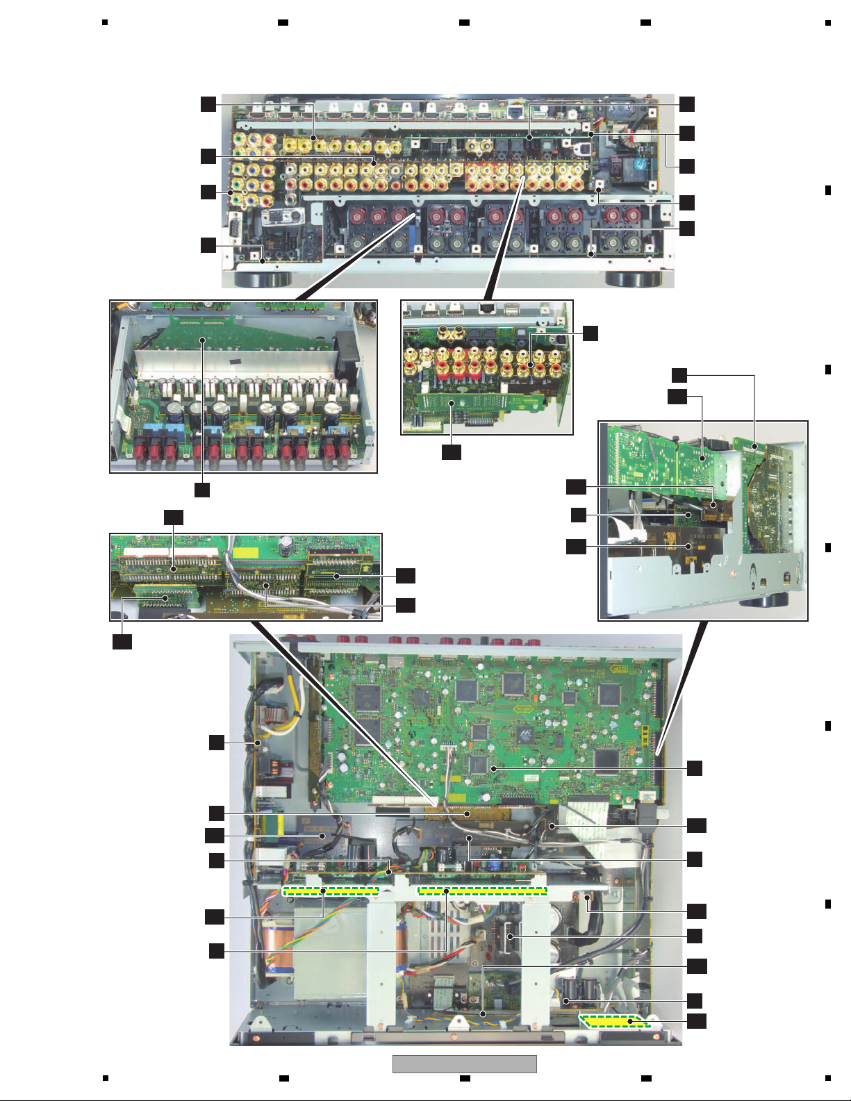
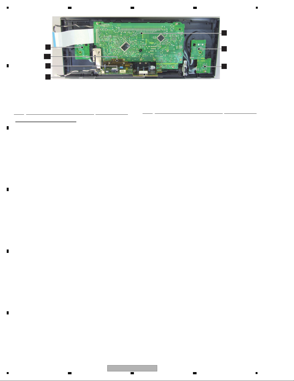
3.2 PCB LOCATIONS
6 7 8
A
B
C
D
E
F
SC-68
5
6 7 8
11
Page 12
1
VOL ASSY
ENCODER ASSY
DISPLAY ASSY
POWER SW ASSY
FRONT HDMI USB
ASSY
C
PANEL GUARD
ASSY
MIC HP ASSY
K
M
AP
O
L
N
NOTES: - Parts marked by “NSP” are generally unavailable because they are not in our Master Spare Parts List.
-
The > mark found on some component parts indicates the importance of the safety factor of the part.
Therefore, when replacing, be sure to use parts of identical designation.
A
B
2 3 4
Mark No. Description Part No.
Mark No. Description Part No.
LIST OF ASSEMBLIES
NSP 1..D AMP ASSY (SC-68) AWH7052
2..D AMP ASSY AWX1214
NSP 1..D AMP ASSY (SC-67) AWH7056
2..D AMP ASSY AWX1218
C
NSP 1..IR BUFFER ASSY AWM8307
2..IR BUFFER ASSY AWX1170
2..BUFFER GND ASSY AWX1171
NSP 1..PRIM DISPLAY ASSY AWM8300
2..DISPLAY ASSY AWX1133
2..VOL ASSY AWX1134
2..POWER SW ASSY AWX1135
2..PRIMARY ASSY AWX1142
2..MIC HP ASSY AWX1149
2..ENCODER ASSY AWX1150
2..MIC HP GUARD ASSY AWX1152
D
E
F
2..FAN CONNECT ASSY AWX1197
NSP 2..VREG GUARD ASSY AWX1153
NSP 2..PANEL GUARD ASSY AWX1154
NSP 1..AUDIO COMPOSITE ASSY (SC-68) AWR7141
2..AUDIO ASSY AWX1119
2..COMPOSITE ASSY AWX1125
2..D-AUDIO BRIDGE ASSY AWX1127
2..D-DAC BRIDGE ASSY AWX1128
2..A-DAC BRIDGE ASSY AWX1129
NSP 1..AUDIO COMPOSITE ASSY (SC-67) AWR7144
2..AUDIO ASSY AWX1122
2..COMPOSITE ASSY AWX1126
2..D-AUDIO BRIDGE ASSY AWX1127
2..D-DAC BRIDGE ASSY AWX1128
2..A-DAC BRIDGE ASSY AWX1129
NSP 1..INTERFACE REG ASSY (SC-68) AWR7150
2..INTERFACE ASSY AWX1172
2..IR REG ASSY AWX1173
2..B DIODE ASSY AWX1174
2..PRE BRIDGE ASSY AWX1177
2..A REG BRIDGE ASSY AWX1178
NSP 2..BIND B CABLE ASSY AWX1179
NSP 2..FFC GUARD ASSY AWX1176
12
1
2 3 4
SC-68
NSP 1..INTERFACE REG ASSY (SC-67) AWR7155
2..INTERFACE ASSY AWX1172
2..IR REG ASSY AWX1173
2..B DIODE ASSY AWX1174
2..PRE BRIDGE ASSY AWX1177
2..A REG BRIDGE ASSY AWX1178
2..PRIMARY SHIELD ASSY AWX1175
NSP 2..BIND B CABLE ASSY AWX1179
NSP 2..FFC GUARD ASSY AWX1176
NSP 1..REG BRIDGE ASSY (SC-68) AWR7151
2..REG ASSY AWX1180
2..FRONT BRIDGE ASSY AWX1181
2..DISPLAY BRIDGE ASSY AWX1182
2..F-IN BRIDGE ASSY AWX1183
2..MULTI CH IN ASSY AWX1184
2..MCH BRIDGE ASSY AWX1185
2..FB-CONNECT ASSY AWX1186
2..CONNECT ASSY AWX1187
2..USB RECT ASSY AWX1188
2..BIND DM CABLE ASSY AWX1189
NSP 1..REG BRIDGE ASSY (SC-67) AWR7153
2..REG ASSY AWX1180
2..FRONT BRIDGE ASSY AWX1181
2..DISPLAY BRIDGE ASSY AWX1182
2..F-IN BRIDGE ASSY AWX1183
2..FB-CONNECT ASSY AWX1186
2..CONNECT ASSY AWX1187
2..USB RECT ASSY AWX1188
2..BIND DM CABLE ASSY AWX1189
1..USB DAC ASSY (SC-68) AWX1097
1..DAC HIGH ASSY (SC-68) AWX1104
1..DAC HIGH ASSY (SC-67) AWX1109
1..COMPONENT ASSY (SC-68) AWX1106
1..COMPONENT ASSY (SC-67) AWX1107
1..FRONT HDMI USB ASSY AWX1111
1..IR INTERFACE_M ASSY AWX1169
1..DIGITAL MAIN ASSY (SC-68) AWX9904
1..DIGITAL MAIN ASSY (SC-67) AWX1198
Page 13
[1] Jigs List
[2] Lubricants and Glues List
Name Jig No. Remarks
39P FFC
extension jig cable
GGD1681
15P FFC
extension jig cable
GGD1680
Diagnosis for AUDIO ASSY, D AMP ASSY
20P + 14P board to board extension jig cable GGD1798
23P + 23P board to board extension jig cable GGD1804
Diagnosis for AUDIO ASSY, D AMP ASSY
5P PH Housing ASSY
extension jig cable
GGD1594
Diagnosis for AUDIO ASSY, D AMP ASSY
23P board to board extension jig cable GGD1805
Diagnosis for DIGITAL MAIN ASSY, DAC HIGH ASSY
27P board to board extension jig cable GGD1799
Diagnosis for DIGITAL MAIN ASSY, DAC HIGH ASSY
30P + 28P board to board extension jig cable GGD1806
Diagnosis for DIGITAL MAIN ASSY, DAC HIGH ASSY
28P + 14P board to board extension jig cable GGD1763
Diagnosis for DAC HIGH ASSY
Diagnosis for AUDIO ASSY, D AMP ASSY,
DIGITAL MAIN ASSY, DAC HIGH ASSY
Diagnosis for AUDIO ASSY, D AMP ASSY,
DIGITAL MAIN ASSY, DAC HIGH ASSY
Name
Lubricants and Glues No.
Remarks
Silicone Grease
ZLB-PN397B
Refer to “9.5 FRONT SECTION”
5
6 7 8
3.3 JIGS LIST
A
B
C
D
E
F
SC-68
5
6 7 8
13
Page 14
1
23.FR+
22.FR-
21.GNDFR
20.V+12FR
19.V-12FR
18.FL+
17.FL-
16.GNDFL
15.V+12FL
14.V-12FL
13.C+
12.C-
11.GNDC
10.V+12C
9.V-12C
8.FHR+
7.FHR-
6.GNDFHR
5.V+12FHR
4.V-12FHR
3.FHL+
2.FHL-
1.GNDFHL
20
27
20
15/60
9/65
TUNER
MODULE
3/100
*2mm
39/120
1.FRONTV
2.GNDF
2
1.ACWP
2.GNDV
3.GNDV
4.V+5_V
5.-VF
6.FL AC2
7.FL AC1
15/330
19.EXSO
18.EXBCK
17.EXOE
16.EXST
15.XOLERR
14.XBERR
13.IRMUTEA
12.IRMUTESB
11.IRMUTEFH
10.RY_FW
9.RY_AF
8.RF_CR
7.RF_FH
6.RF_B
5.AMP_TEMP
4.XTEMPSD5
3.XDCERR
2.GNDD
1.GNDD
19/90
*1.00mm
555 5
ADD7747-
ADD7745-
ADD7725-
ADD7781-
ADD7753-
D20PYY0310E
*1.00mm
CN8301
CN3472
CN3001
JH3004
JH3002
CN7006
CN4000
JP3001
CN7723
CN2503
CN7724
CN3601
CN8303
JP7725
JP8402 CN8401
CN6803 CN68
CN3CN3802
23 2
223
CN4002
CN4003
CN4004
2
4
7
*3
5555
CN3870
CN3880CN3890
CN
CN3860
CN4700
CN4100CN4200 CCN4600
JP3001
CN3004
ADD7763-
7/60
6
CN3371
J3004
14
CN3001
CN3902
CN7722
717
CN7721
14
CN3792
14
CN3791
14
CN7802
19
CN7801
13
CN7803CN7804
27 19
717
CN7684
CN7683
717
CN7682CN7681
717
CN7002 CN7007
13
CN7004 CN7003
7
CN7005
15
CN7008
157
CN7661CN7662
7
1.XFANERR
2.FANCTLL
3.FANCTLH
4.EXSO
5.EXSCK
6.EXOE
7.EXST
8.XOLERR
9.AMP_TEMP
10.IRMUTEA
11.IRMUTESB
12.IRMUTEFH
13.RY_FW
1.XFANERR
2.FANCTLH
3.FANCTLL
4.XMICDET
5.V-7_A
6.GNDA
7.GNDA
8.V+7_A
9.MICOUT
10.GNDA
11.HPL
12.GNDHP
13.GNDHP
14.HPR
15.GNDHP
16.AMUTE
17.XHPDET
7.FLAC1
6.FLAC2
5.-VF
4.V+12TRG
3.V+5_V
2.GNDV
1.GNDV
1.FLAC1
2.FLAC2
3.-VF
4.V+5_V
5.GNDV
6.GNDV
7.ACWP
15.FRONTV
14.GNDF
13.XMICDET
12.V-7_A
11.GNDA
10.V+7_A
9.GNDA
8.MICOUT
7.GNDA
6.HP_L
5.GNDHP
4.HP_R
3.GNDHP
2.AMUTE
1.XHPDET
CN7664
CN3651
CN7663
*1.00mm
CN7902
CN7901
*1.00mm
*1.00mm
1.XHPDET
2.AMUTE
3.GNDHP
4.HPR
5.GNDHP
6.GNDHP
7.HPL
8.GNDA
9.MICOUT
10.GNDA
11.V+7_A
12.GNDA
13.GNDA
14.V-7_A
15.XMICDET
CN602CN603
23.V+12FHL
22.V-12FHL
21.SR+
20 SR
JA9605 CN601
CN901
CN9202
6
*1.00mm
*1.00mm
*1.00mm
ADX7753-
7/240
19/360
ADX7732-
ADX7786-
5/580
ADX7747-
2/120
JP7001
*1.00mm
JA8001 JA8002
iPod Direct USB HDMI IN5
JA3471JA3472
VIDEO MIC IN HEADPHONE
JA3476
MCACC setup
!
FU10
*4
IR
JA7005
OUTRF 5V OUT
JA7002
JA7003
12V TRG1
12V TRG2
IR IN2
JA7001
IR IN1
1.FLAC1
7.GNDV
17.XFANERR
1.XHPDET
3.S7-2
2.NC
1.S7-1
1.FRONTV
15.HP L
3
1.XFANERR
2.FANCTLL
3.FANCTLH
15.XHPDET
1.XMICDET
(DVR) (DVD)
JA8301JA8304
JA8601
IN1
PR
PB
YY
PB
PR
232C MONITOR IN2
OUT
1.V-5_V
2.GNDV
3.V+5_V
4.GNDV
5.ZONE3_OUT
6.GNDV
7.ZONE2_OUT
8.GNDV
9.DVR_OUT
10.GNDV
11.MONITOR_OUT
12.GNDV
13.DVR_IN
14.GNDV
15.VIDEO_IN
16.GNDV
17.TV/SAT_IN
18.GNDV
19.DVD_IN
20.GNDV
OUT
IN
DVRSAT DVR
OUT
JA3602JA3605
IN
JA3601JA3603
ZONE2 DVD
OUTIN
MONITOR
OUT
JA3604
ZONE3
PR
JA8305
OUT
ZONE2
Y
PB
SAT
ININ
DVD
DVR
INOUT
JA2504
JA2501
OUT
ZONE3
JA3
206
IN
PHONO
JA2503
IN3 IN4
JA9602JA9606
JA9603JA1603 JA9601
IN1ZONE4 OUT
BD IN
FRONT
CENTER
JA4101
F-HEIGHT
RL LR
for IC3001 DBUG&D.L.
CN3002
J0002
J0006
J0001
J0007
J0004
J0005
Y0026
CN3652
1.TURST
2.TUSDA
3.TUSCL
4.TUIREQ
5.NC
6.GNDT
7.TR
8.V+5T
9.TL
IN2
JA9607
D
JH3003
JA5101
OUT
ZONE2
JA6701
IN5
IN6
JA9604
PR
JA8302
(VIDEO)
IN3
Y
PB
VIDEO
IN
JA2502
VIDEO
IN
23
CN3771
CN1502
23
23.Z2HPF
1.FHMUTE
23
CN3772
CN2861
23
SW
15
15
1.RY_AF
2.RY_CR
3.RY_FH
4.RY_B
5.XBERR
6.XTEMPSD5
7.XDCERR
8.GNDD
9.GNDD
10.12VTRG1
11.12VTRG2
12.12VERR
13.RF_POW
14.GNDD
15.IR_IN
16.V+5R6_EV
17.V+5R6_EV
18.GNDD
19.GNDD
19
19
39/140
J0003
ADD7746-
2/205
ADX7776-
*1.25mm
1.XFANERR
39.V+5R6_EV
JA7004
16.OSDSCK
17.OSDCS
18.XOSDRST
19.GNDD
20.232POW
21.232CDET
22.EV232TX
23.EV232RX
24.GNDD
25.GNDD
26.V+5R6_EV
27.V+5R6_EV
39.XFANERR
38.AMPTEMP
37.WUSBPOW
36.XNETRST
35.IRIN
34.XDCERR
33.XOLERR
32.XBERR
31.232CDET
30.232POW
29.232EV
28.EV232TX5
27.EV232RX5
26.XWUSBERR
25.CECIO
24.HOTPLUG
23.NETWOL
22.TEMPERR
21.NC
20.EVREQI5
19.EVSCK
18.EVSO
17.EVSI5
16.XEMRST5
15.EVREQO
14.NETPOW
13.DVCPOW
12.FHD5VEN
11.MHLPOW
10.XMHLPERR
9.ACRY
8.XSMUTE
7.LOWPOW
6.GNDD
5.GNDD
4.GNDD
3.GNDD
2.V+5R6_EV
1.V+5R6_EV
6.GNDD
5.USBPOW
4.XUSBERR
3.D+
2.D-
1.GNDD
1.GNDD
2.Y_IN
3.GNDD
4.CB_IN
5.GNDD
6.CR_IN
7.GNDD
8.CVBS_IN
9.GNDD
10.V+5_V
11.V+5_V
12.COMP_DET
13.SDA
14.SCL
15.OSDSO
1 Z2HPF
2 RECMUTE
3 TUIREQ
4 TURST
5 TUSDA
6 TUSCL
7 GNDD
8 Z_SIG_DET
9 GNDD
10 GNDD
11 VLSCK
12 VLSO
13 Z2VLSO
14 Z3MUTE
15 Z2MUTE
16 SBMUTE
17 AMUTE
18 PRESEL
19 LSSN
20 XMICDET
21 RYHP
22 XHPDET
23 FHMUTE
19.V+5R6_EV
18.V+5R6_EV
17.GNDD
16.GNDD
15.XFANERR
14.FANCTLL
13.FANCTLH
12.EXSO
11.EXSCK
10.EXOE
9.EXST
8.GNDD
7.AMPTEMP
6.IRMUTEA
5.IRMUTESB
4.IRMUTEFH
3.RFPOW
2.RYFW
1.GNDD
15.GNDD
14.RYAF
13.RYCR
12.RYFH
11.RYB
10.XBERR
9.XTEMPSD5
8.XDCERR
7.XOLERR
6.GNDD
5.12VTRG1
4.12VTRG2
3.12VERR
2.GNDD
1.IRIN
1.GNDD
2.BTPOW
3.BTOL
4.BTRX
5.BTTX
6.BTDET
7.GNDD
BT ADAPTER
PORT
JA2102
14.BT L
1.V-12_A
CN2104
L
R
28.GNDADS
27.FR IN
26.GNDADS
25.FL IN
24.GNDDAS
23.FR OUT
22.GNDDAS
21.FL OUT
20.GNDDAS
19.SW OUT
18.GNDDAS
17.C OUT
16.GNDDAS
15 SR OUT
14.BT L
13.GNDBT
12.BT R
11.GNDBT
10.V+6_AD
9.V+6_AD
8.GNDAD
7.GNDAD
6.V+12_A
5.V+12_A
4.GNDA
3.GNDA
2.V-12_A
1 V 12 A
39.XFANERR
1.V+5_EV
21.EVSO
22.EVSI5
23.XWUSBERR
24.WUSBPOW
25.EVREQO
26.NETPOW
27.DVCPOW
28.FHD5VEN
29.MHLPOW
30.XMHLPERR
31.XNETRST
32.XEMRST5
33.XOLERR
34.GNDD
35.GNDD
36.GNDD
37.GNDD
38.V+5_EV
39.V+5_EV
1.XFANERR
2.AMPTEMP
3.XDCERR
4.XBERR
5.IRIN
6.232CDET
7.232POW
8.232EV
9.EV232TX5
10.EVREQI5
11.TEMPERR5
12.EV232RX5
13.HOTPLUG
14.XSMUTE
15.CECIO
16.LOW_P
17.NETWOL
18.XRESET
19.ACRY
20.EVSCK
1.V+5_EV_1
2.POWLED
3.POWER KEY
4.GNDD
1.JOG_A
2.JOG_B
3.GNDD
7.CEC_IO
6.XVDDERR
5.XMHLPERR
4.MHLPOW
3.FHD5VEN
2.MHLWUP
1.GNDD
1.VOLA
2.VOLB
3.GNDD
1.HP L
2.GNDHP
3.HP R
4.GNDHP
5.AMUTE
6.XHPDET
7.XMICDET
8.V-7_A
9.GNDA
10.GNDA
11.V+7_A
12.GNDA
13.MICOUT
14.GNDF
15.FRONTV
CN8002
JA8003
JP8001
7.CEC_IO
6.XVDDERR
5.XMHLPERR
4.MHLPOW
3.FHD5VEN
2.MHLWUP
1.GNDD
19.V+5_EV
18.V+5F
17.GNDD
16.HPD
15.MHL_CTL
14.SDA_SINK
13.SCL_SINK
12.RFXC-
11.GNDD
10.RFXC+
9.RFX0-
8.GNDD
7.RFX0+
6.RFX1-
5.GNDD
4.RFX1+
3.RFX2-
2.MHL_DET
1.RFX2+
CN8001
6.GNDD
5.USBPOW
4.XUSBERR
3.D+
2.D-
1.GNDD
2.GNDUSB
1.V+UN_USB
UXJCB
AXX7282-
*3
SYXJ8
JXJ
DLPWXJ,FXJ,AXJ5
TUNER
AXX7283-
-
MODEL
ADX7795-
Y0028
*1.25mm
Y0027
*1.25mm
*1.25mm
*1.25mm
*1.25mm
*1.25mm
*1.25mm
*1.25mm
*1.25mm
*1.25mm
WRAPPED TAPE
A
A
1/3 -A3/3
( )
AUDIO ASSY
(SC-68 : AWX1119)
(SC-67 : AWX1122)
Y
CONNECT ASSY
(AWX1187)
Z
AJ
AL
AM
AN
AO
H
R
P
FFC GUARD ASSY
(AWX1176)
VREG GUARD ASSY
(AWX1153)
INTERFACE ASSY
(AWX1172)
IR BUFFER
ASSY
(AWX1169)
IR INTERFA
(AWX1170
FB-CONNECT
ASSY
(AWX1186)
MIC HP GUARD ASSY
(AWX1152)
BIND DM CABLE ASSY
(AWX1189)
BIND B CABLE ASSY
(AWX1179)
G
G
1/11 -G1
(
DIGITAL MAIN AS
(SC-68 : AWX9904
(SC-67 : AWX1194
L
DISPLAY ASSY
(AWX1133)
M
VOL ASSY
(AWX1134)
C
FRONT HDMI USB ASSY
(AWX1111)
K
MIC HP ASSY
(AWX1149)
J
COMPOSITE ASSY
(SC-68 : AWX1125)
(SC-67 : AWX1126)
AP
PANEL GUARD ASSY
(AWX1154)
AE
FRONT BRIDGE
ASSY
(AWX1181)
AD
D
(
AC
D-AUDIO BRIDGE ASSY
(AWX1127)
AA
PRE BRIDGE ASSY
I
COMPONENT ASSY
(SC-68 : AWX1106)
(SC-67 : AWX1107)
D
USB RECT
ASSY
(AWX1188)
AG
F-IN BRIDGE ASSY
(AWX1183)
AF
DISPLAY BRIDGE ASSY
(AWX1182)
I
1/2 -I2/2
( )
L
1/2 -L2/2
( )
2 3 4
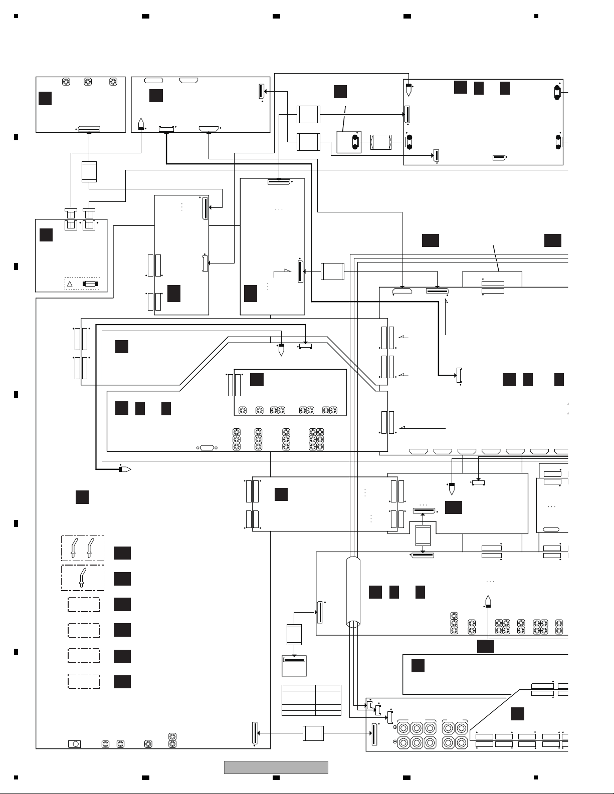
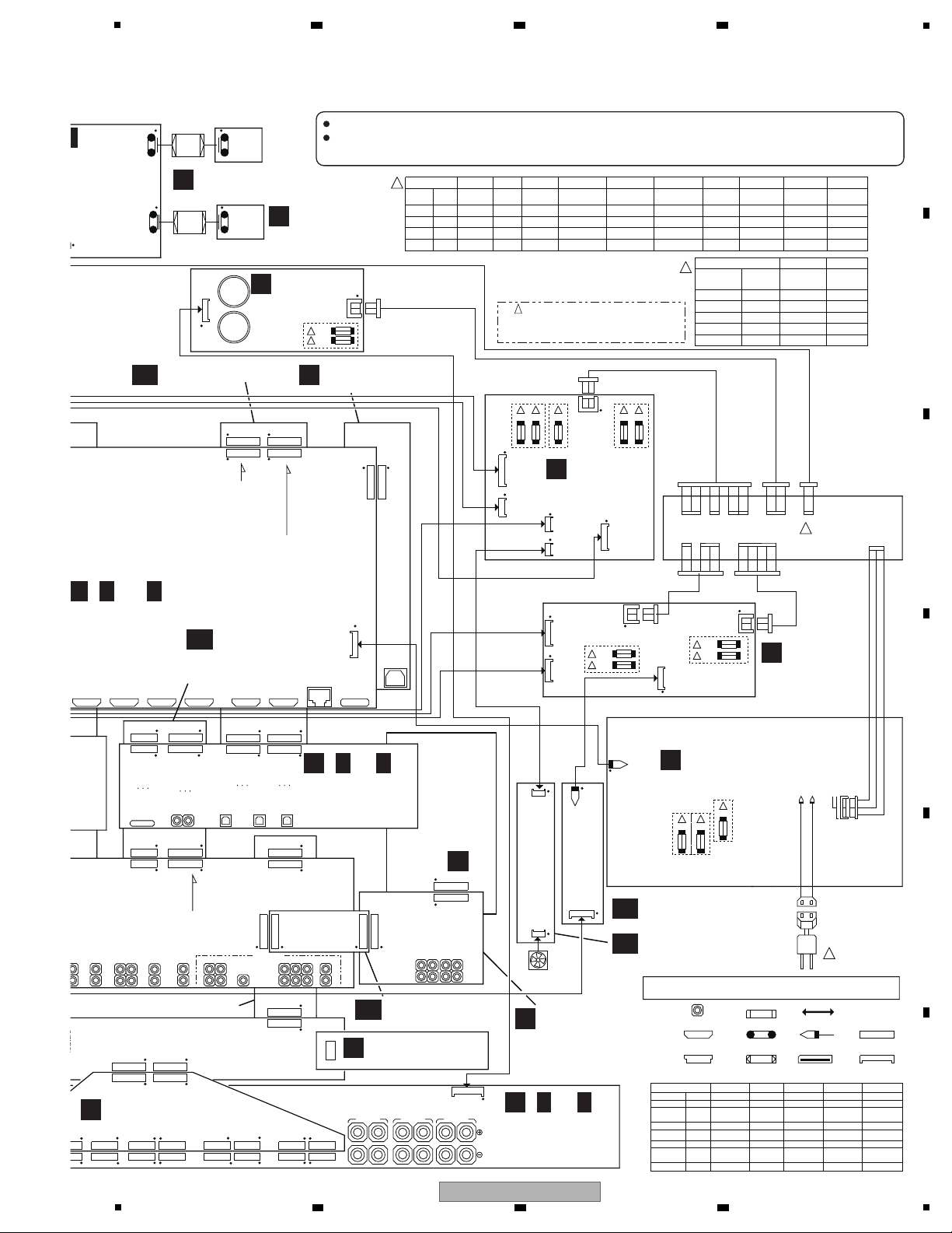
4. BLOCK DIAGRAM
4.1 OVERALL WIRING DIAGRAM
A
B
C
D
E
F
14
1
2 3 4
SC-68
Page 15
5
23
16.GNDFL
15.V+12FL
14.V-12FL
13.C+
12.C-
11.GNDC
10.V+12C
9.V-12C
8.FHR+
7.FHR-
6.GNDFHR
5.V+12FHR
4.V-12FHR
3.FHL+
2.FHL-
1.GNDFHL
23
23
3
!
AC CORD
SECONDARY
PRIMARY
4/100
7
5
1.-B+15V
2.-B
1.V+12_DF
2.GND_DF
3.V-12_DF
4.GND_DF(S)
5.V+12_RY
6.V-12_RY
7.V-12_RY
3
2
FAN
B-DIODEIR REG
REG
REG
USB RECT
3.LOCKDET
2.V-FAN
1.V+FAN
4
55 555
!
FU32
!
FU31
!
FU21
!
FU22
1.V+8_MD
2.GND_MD
3.V-8_MD
4.GND_MD(S)
4
!
FU12!FU11
!
FU15
!
FU14!FU13
ADX7746-
4/195
D20PYY0410E
ADX7755-
4/375
ADX7759-
3/190
!
4.-B
3.GND
2.GND
1.+B
JH3002
CN4001
CN3051
CN6952
CN6801
CN6951
CN7401
CN7400
CN7201
CN7251CN7241
CN7271
CN7281
CN7502
CN7603
CN6803 CN6802
CN3801CN3802
23 23
2323
*1
*4
*4
*4
!
*4
AXM7040-
*1
!
BOARD IN
FFC
2.0mm FLAT CABLE FFC CONNECTOR
2.0mm CABLE HOLDER
*2mm
BOARD TO BOARD
T1501
CAUTION - FOR CONTINUED PROTECTION AGAINST RISK OF FIRE,
REPLACE WITH SAME TYPE AND RATINGS OF FUSE.
4.-B(+65V)
3.GND
2.GND
1.+B(+65V)
55555
CN3870
CN3840
CN3850
CN3860
CN4700
CN7601
CN7501
S2,S3,S9
S5,S6
S4
S1
S7
4
23
ANOTHER CONNECTOR
CN3401
J3002
JUMPER CONNECTOR
28
CN2502
14
CN3001
18
CN251018CN7671
18
CN767218CN7761
2814
CN3794CN3792
2814
CN3793CN3791
2830
CN3783 CN3781
2814
3028
CN3784
3028
CN3782
2830
V-REG A-REG
23.V+12FHL
22.V-12FHL
21.SR+
20.SR-
19.GNDSR
18.V+12SR
17.V-12SR
16.SL+
15.SL-
14.GNDSL
13.V+12SL
12.V-12SL
11.SBR+
10.SBR-
9.GNDSBR
8.V+12SBR
7.V-12SBR
6.SBL+
5.SBL-
4.GNDSBL
3.V+12SBL
2.V-12SBL
1.GNDCH
18.GNDA
17.GNDA
16.SBL IN
15.GNDA
14.SBR IN
13.GNDA
12.SL IN
11.GNDA
10.SR IN
9.GNDA
8.C IN
7.GNDA
6.SW IN
5.GNDA
4.FL IN
3.GNDA
2.FR IN
1.GNDA
23.PRESEL(W/XF)
22.V+7_A
21.V-7_A
20.GNDA
19.GNDA
18.SR OUT
17.GNDA
16.SL OUT
15.GNDA
14.FR OUT
13.GNDA
12.C OUT
11.GNDA
10.FL OUT
9.GNDA
8.FH/FWR OUT
7.GNDA
6.FH/FWL OUT
5.GNDA
4.SBR OUT
3.GNDA
2.SBL OUT
1.GNDA
HDMI CONNECTOR
CN9002 CN9003
CN9501
CN7602
7
1.V+5_V
2.GNDV
3.GNDV
4.V-5_V
ADX7791-
7/205
JP51
ADX7729-
7/75
1.FLAC1
2.FLAC2
3.-VF
4.V+12TRG
5.GNDV
6.GNDV
7.V+5_V
5.V-12_A
4.GNDA
3.GNDA
2.V+12_A
1.V+6_AD
ADX7745-
5/150
1.XFANERR
2.FANCTLL
3.FANCTLH
*4 *4
*4
FU4
FU1
!
!
*4
JA71_1 WHT
JA71 YEL
PIN JACK
MODEL AC CORDMAIN TRANS
UXJCB
JXJ
DLPWXJ
AXJ5
FXJ
SYXJ8
1.S1-1
2.S1-C
3.S1-2
1.S3-1
2.S3-C
3.S3-2
4.S2-1
5.S2-2
6.S9-1
7.S9-C
8.S9-2
JA7761 JA7762
R
FCLSSB
5.S6-2
4.S6-1
3.S5-2
2.S5-C
1.S5-1
1.S4-1-1
2.S4-2-1
3.S4-C
4.S4-2-2
5.S4-1-2
IN
R
C&SWF
JA3101 JA3202
DVR
INFWOUT
JA2504
JA32011
PRE OUT
SBSLFH
IN
PHONO
IN
JA2503
CD
JA9201
IN3 IN4
IN7
OUT 2
JA9202
LAN
JA9602 JA9603 JA9608 JA1602
RL
SURROUND
JA4301LRJA4901
S-BACK
JA4501
*4
FU2
!
MAIN TRANS
MODEL
AXJ5
JXJ
FXJ
DLPWXJ
FU61,FU62FU11,FU12 FU13,FU14 FU15
FU1 FU4
FU31,FU32
FU2
FU21,FU22
-
-
-
-
FU10
*OPTION
MODEL
AXJ5
UXJCB
SYXJ8
JXJ
FXJ
DLPWXJ
MICROPHONE REMO-COM iPod CABLE
Y0020
Y0023
UXJCB
SYXJ8
DLPWXJ
AXJ5
FXJ
JXJ
SYXJ8
-
SHIELD CABLE
3
3.LOCKDET
2.V-FAN
1.V+FAN
3
CN7291
1.V+FAN
2.V-FAN
3.LOCK DET
USB
for WLAN
D20PYY0310E
3/100
JH3003
J3003
CN3501
*2mm
FU62
FU61
!
!
*4
F-WIDE/B
LR
55
5
CN3820
CN4900
5
CN3810
CN4800
KN6962
JA3102
SW2
3/110
CN5932 CN5931
JP5775
5
5.V-12_A
4.GNDA
3.GNDA
2.V+12_A
1.V+6_AD
CN5775
5.V-12_A
4.GNDA
3.GNDA
2.V+12_A
1.V+6_AD
5/60
ADX7773-
WIFI CABLE
-
-
-
-
-
-
-
-
-
-
-
IN6
JA9604 JA1601
OUT 1
ADX7766-
17
CN5501
17
CN9801
1.USBDPON
2.XRT_USB_B
3.GNDD
4.USBMCLK
5.GNDD
6.USBLRCK
7.GNDD
8.USBBCK
9.GNDD
10.USBADAT
11.V+3R3_USB
12.V+3R3_USB
13.GNDD
14.GNDD
15.SCL_USB_B
16.SDA_USB_B
17.INT_USB_B
USB-DAC
IN
JA5501
VIDEO
IN
JA2502
20.EVREQI5
19.EVSCK
18.EVSO
17.EVSI5
16.XEMRST5
15.EVREQO
14.NETPOW
13.DVCPOW
12.FHD5VEN
11.MHLPOW
10.XMHLPERR
9.ACRY
8.XSMUTE
7.LOWPOW
6.GNDD
5.GNDD
4.GNDD
3.GNDD
2.V+5R6_EV
1.V+5R6_EV
12 VLSO
13 Z2VLSO
14 Z3MUTE
15 Z2MUTE
16 SBMUTE
17 AMUTE
18 PRESEL
19 LSSN
20 XMICDET
21 RYHP
22 XHPDET
23 FHMUTE
1.BADA
2.SADA
3.CADA
4.FADA
5.DABCK
6.DALRCK
7.FHADA
8.GNDD
9.DAMCK
10.GNDD
11.ZMCLK
12.GNDD
13.ZBCK
14.ZFADA
15.ZLRCK
16.GNDD
17.DIRMCKO
18.GNDD
19.DIRLRCK
20.DIRDATO
21.DIRINT
22.DAC0DET
23.GNDD
24.DIRMCKI
25.GNDD
26.DIRBCK
27.GNDD
28.MSPDIF
1.GNDD
2.BTPOW
3.BTOL
4.BTRX
5.BTTX
6.BTDET
7.GNDD
8.V+3R3_D
9.V+3R3_D
10.GNDD
11.GNDD
12.V+5_D
13.V+5_D
14.DIRPOW
15.DSPSO
16.DSPSCK
17.RYAC
18.ZDZF
19.XZ2DARST
20.XDARST
21.DACS
22.F96K
23.F192K
24.XADRST
25.XTLO
26.XDIRRST
27.DSPSI
28.DIRCS
29.UNLK
30.DAZDB
1.V+5R6_EV
2.V+5R6_EV
3.V+5R6_EV
4.GNDD
5.GNDD
6.GNDD
7.RYAC
JA2003
30.GNDD
1.DAZDB
BT ADAPTER
PORT
CN2103
OPT IN1IN1
28.BADA
1.MSPDIF
JA2008
OPT OUT1
COAX
CN2102
IN2
JA2006
JA2102
JA2002
OPT IN2
28.GNDADS
1.ZL OUT
14.BT L
1.V-12_A
CN2101CN2104
JA2505
28.GNDADS
27.FR IN
26.GNDADS
25.FL IN
24.GNDDAS
23.FR OUT
22.GNDDAS
21.FL OUT
20.GNDDAS
19.SW OUT
18.GNDDAS
17.C OUT
16.GNDDAS
15.SR OUT
14.GNDDAS
13.SL OUT
12.GNDDAS
11.FHR/FWR OUT
10.GNDDAS
9.FHL/FWL OUT
8.GNDDAS
7.SBR OUT
6.GNDDAS
5.SBL OUT
4.GNDDAS
3.ZR OUT
2.GNDDAS
1.ZL OUT
14.BT L
13.GNDBT
12.BT R
11.GNDBT
10.V+6_AD
9.V+6_AD
8.GNDAD
7.GNDAD
6.V+12_A
5.V+12_A
4.GNDA
3.GNDA
2.V-12_A
1.V-12_A
1.V+5_EV_1
2.POWLED
3.POWER KEY
4.GNDD
1.JOG_A
2.JOG_B
3.GNDD
(UXJCB,JXJ)
(SYXJ8,DLPWXJ,FXJ,AXJ5)
Y0024
UXJCB
SC-68
SC-67
SC-LX86
SC-LX76
SC-LX86
SC-LX76
SC-LX86
SC-LX76
SC-LX86
SC-LX76
REK1154(10A/125V)
AEK1061(T5A L/250V)
AEK1061(T5A L/250V)
DEK1045(T10A L/250V)
AEK7078-
(10A/125V)
REK1139-
(T2A H/250V)
REK1104(T4A H/250V)
REK1104(T4A H/250V)
REK1139-
(T2A H/250V)
REK1139-
(T2A H/250V)
AEK1061(T5A L/250V)
AEK1061(T5A L/250V)
AEK1061(T5A L/250V)
REK1151(6A/125V)
REK1151(6A/125V)
REK1143(1.25A/125V)
REK1143(1.25A/125V)
AEK7073(T1A L/250V)
AEK7073(T1A L/250V)
AEK7073(T1A L/250V)
AEK7072(T800mA L/250V)
AEK7072(T800mA L/250V)
AEK7072(T800mA L/250V)
REK1142(1A/125V)
REK1142(1A/125V)
REK1143-
(1.25A/125V)
REK1143(1.25A/125V)
AEK7073(T1A L/250V)
AEK7073(T1A L/250V)
AEK7073(T1A L/250V)
AEK7072(T800mA L/250V)
REK1143-
(1.25A/125V)
REK1143-
(1.25A/125V)
AEK7072(T800mA L/250V)
AEK7072(T800mA L/250V)
REK1143(1.25A/125V)
REK1143-
(1.25A/125V)
AEK7073(T1A L/250V)
AEK7073-
(T1A L/250V)
AEK7073-
(T1A L/250V)
SC-LX76
SC-LX86
SC-LX76
SC-67
SC-LX76
SC-LX86
SC-LX86
SC-68
SC-LX76
SC-LX86
SC-LX86
SC-LX76
ADG7118-A
ADG7119-A
ADG7120-A
ADG7119-A
ADG7122-A
ADG7121-A
ATS7438-A
ATS7447-A
ATS7439-A
ATS7448-A
ATS7441-A
ATS7450-A
ATS7439-A
ATS7448-A
ATS7439-A
ATS7448-A
ATS7440-A
ATS7449-A
MHL CABLE
SC-67
SC-68
SC-LX86
SC-LX86
SC-LX86
SC-LX76
SC-LX76
SC-LX76
APM7009APM7009-
APM7009-
APM7009-
APM7010-
APM7010-
APM7010-
APM7010-
AXD7612-
AXD7612-
AXD7613-
AXD7613-
AXD7613-
AXD7613-
AXD7614-
AXD7614-
ADE7139ADE7139-
ADE7139-
ADE7139-
ADE7139ADE7139-
ADE7139-
ADE7139-
ADE7136ADE7136-
ADE7136-
ADE7136-
ADE7136ADE7136-
ADE7136-
ADE7136-
ADE7137-
ADE7137-
4
5
CN5751
5
CN7762
S
S
1/7 -S7/7
( )
D AMP ASSY
(SC-68 : AWX1214)
(SC-67 : AWX1218)
AH
AI
Q
P
T
W
BUFFER GND ASSY
(AWX1171)
IR INTERFACE_M ASSY
(AWX1170)
PRIMARY ASSY
(AWX1142)
IR REG ASSY
(AWX1173)
MCH BRIDGE ASSY
(SC-68 : AWX1185)
A REG BRIDGE ASSY
(AWX1178)
AK
FAN CONNECT ASSY
(AWX1197)
G
1/11 -G11/11
( )
N
POWER SW ASSY
(AWX1135)
O
ENCODER ASSY
(AWX1150)
ASSY
X
B DIODE
ASSY
(AWX1174)
V
REG ASSY
(AWX1180)
E
MULTI CH ASSY
(SC-68 : AWX1184)
U
PRIMARY SHIELD
ASSY
(SC-67 : AWX1175)
B
B
1/2 -B2/2
( )
DAC HIGH ASSY
(SC-68 : AWX1104)
(SC-67 : AWX1109)
F
USB-DAC ASSY
(SC-68 : AWX1097)
AD
D-DAC BRIDGE ASSY
(AWX1128)
E ASSY
AB
A-DAC BRIDGE ASSY
(AWX1129)
2/2
)
Therefore, when replacing, be sure to use parts of identical designation.
When ordering service parts, be sure to refer to "EXPLODED VIEWS and PARTS LIST" or "PCB PARTS LIST".
The > mark found on some component parts indicates the importance of the safety factor of the part.
!
The mark found on some component parts should be replaced
with same parts(safety regulation authorized) of identical
designation.
6 7 8
A
5
6 7 8
SC-68
B
C
D
E
F
15
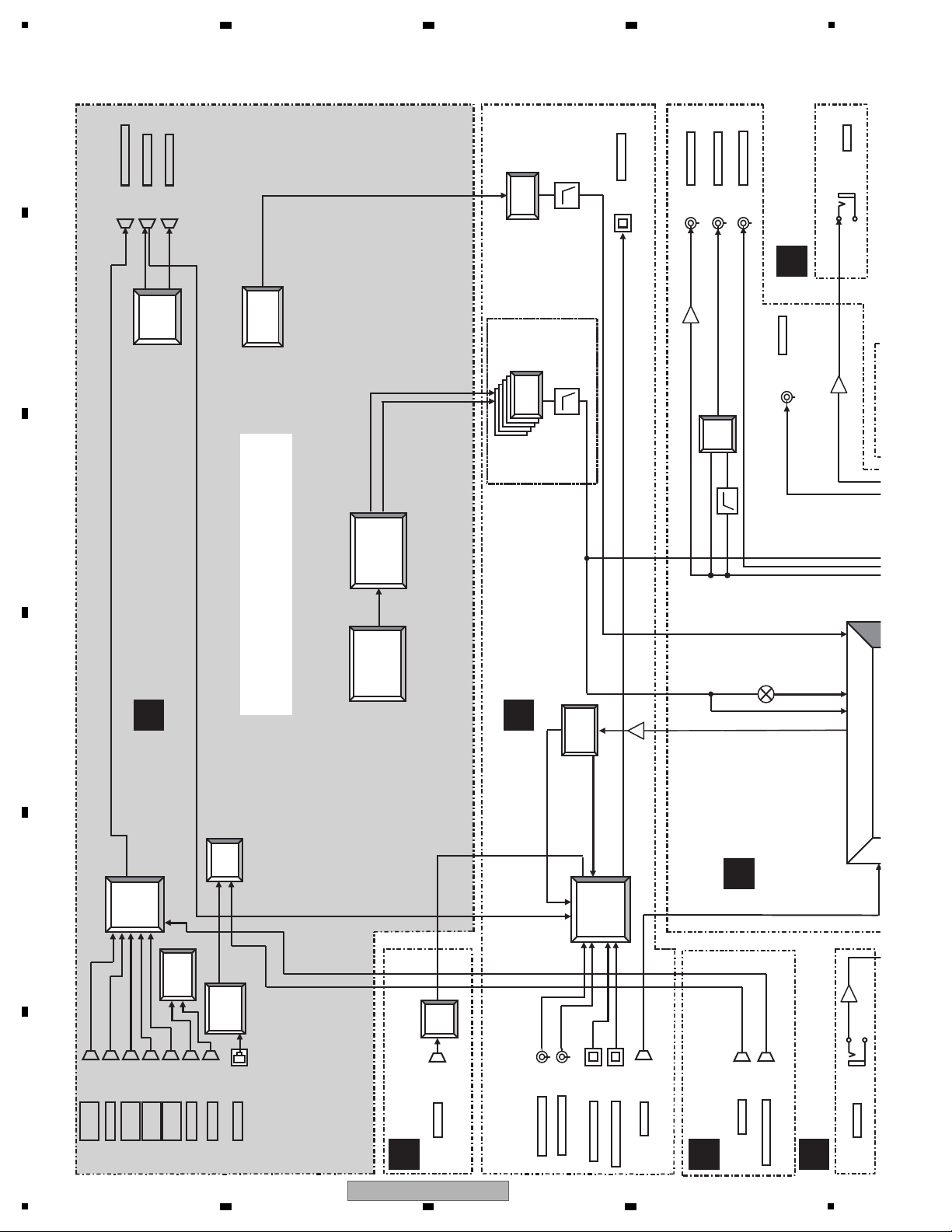
Page 16
1
COAX2(SAT/CBL)
OPT IN1(TV)
OPT IN2(DVR/BDR)
COAX1(DVD)
DAC
AK4480EF
X5
TX1
LPF
JA2009
JA2010
JA2011
HDMI IN5(MHL IN)
MIC
DVR OUT
ZONE2 SW OUT
HP
SW DownMix
JA3471
JA8002
IC2701, IC2702
JA6701
JA2504
JA3476
ZONE3 OUT
JA6701
HEADPHONE
AMP
<<AUDIO ZONE OUT>>
MIC Amp
IC3471
NJM4565MD
IC2011(FL,FR)
IC2012(C,SW)
IC2013(SL,SR)
IC2014(SBL,SBR)
IC2017(FHL,FHR)
IC2003(FL,FR)
IC2005(C,SW)
IC2006(SL,SR)
IC2007(SBL,SBR)
IC2018(FHL,FHR)
IC2451
(ZONE2)
LPF
I2S
A/D BUFFER
IC2401,2402
NJM4565MD
USB
JA8001
OPT OUT1
IC2801
NJM4565MD
JA2008
IC2001
DIR&DIT
AK4118AEQ
IC2501
IC2431
ADC
PCM1804DB
I2S(DATA)
I2S(BCK,LRCK)
(SBL,SBR)
(FL,FR,C,SW,SL,SR,FHL,FHR)
IC9204
MNP
DM860A
IC9602
HDMI PORT
PROCESSER
SII9575CTUC
HDMI IN4
(VIDEO)
HDMI IN6
IC903
HDMI RX
SII9233ACTU
HDMI OUT1
IC9002
1st DSP
D808K013CPTP400
IC1609
HDMI
TRANSMITTER
SII9573CTUC
JA9603
JA9604
JA1601
HDMI IN7
JA9608
JA1602
HDMI OUT2
NETWORK
JA9202
IC9203
ETHERNET
PHYCEIVER
LAN8700C-AEZG
I2S(FL,FR)
IC1814
ZONE2
USB/NET
SELECTOR
BD
JA9601
I2S(except FL,FR)
BT
HDMI IN3
(DVR/BDR)
JA9602
HDMI IN2
(SAT/CBL)
JA9607
JA2102
IC9702
2nd DSP
D808K013CPTP400
ZONE2
ZONE2 OUT
JA6701
ZONE2 SW Amp
IC6701
NJM4565MD
IC6703
ZONE2
SELECTOR
IC6702
HPF
IC2471
ZONE2 DAC
AK4388ET
HDMI IN1
(DVD)
JA9606
HDMI ZONE4 OUT
JA1603
USB-DAC
JA5501
IC5503
DIG-AUDIO
IC
I2S
Refer to the “4-4 BLOCK DIAGRAM FOR
DIGITAL MAIN AUDIO BLOCK”
A
B
C
G
K
AUDIO ASSY
DAC HIGH ASSY
FRONT HDMI
USB ASSY
DIGITAL MAIN ASSY
MIC HP ASSY
K
MIC HP ASSY
F
USB DAC ASSY
2 3 4
4.2 BLOCK DIAGRAM FOR AUDIO BLOCK
• SC-68
A
B
C
D
E
F
16
1
SC-68
2 3 4
Page 17
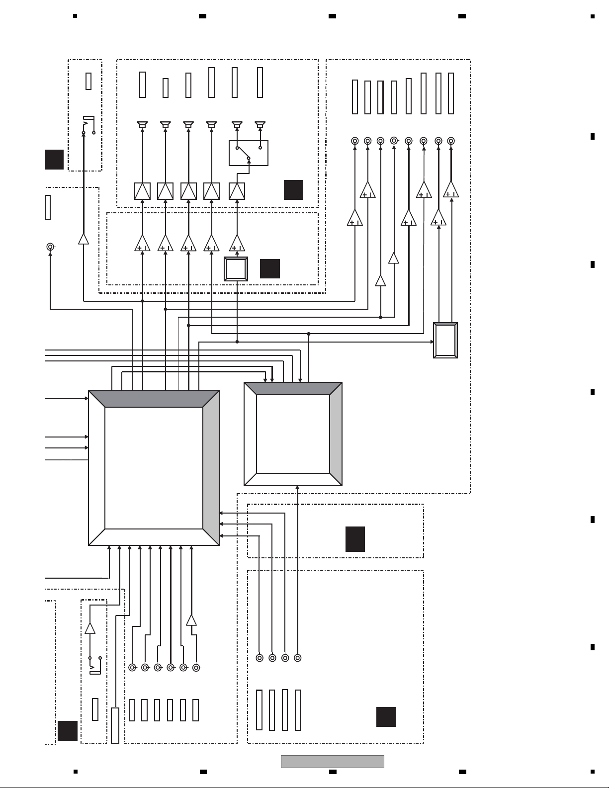
MIC
TV/SAT
VIDEO
CD
PREOUT FL/FR
PREOUT SW1
PREOUT SL/SR
PREOUT SBL/SBR
DVR OUT
SP FL/FR
SP C
SP SL/SR
SP SBL/SBR
HP
SW DownMix
JA3471
IC2701, IC2702
JA2502
JA2504
SW PRE Amp
IC2751
<<POWER AMP>>
JA2504
JA3476
JA4101
JA4101
JA4301
JA4501
JA3101
JA3101
JA3201
JA3201
PREOUT C
JA3101
DVD
DVR
JA2501
JA2501
HEADPHONE
AMP
<<POWER AMP
INPUT BUFFER>>
IC6821,
IC6841
IC6801
IC6861,
IC6881
IC6901,
IC6921
<<PREOUT>>
MIC Amp
IC3471
NJM4565MD
NJM4565MD
IC2801
NJM4565MD
JA2505
PREOUT FHL/FHR
JA3201
IC3221
PRE SELECTOR
SP FHL/FHR
JA4901
RY4500,RY5000
TUNER Module
IC3271
IC2501
Selector / Volume / PRE Amp
BD3473KS2
IC7491
L/R
SELECTOR
SW PRE Amp
IC2751
NJM4565MD
JA3102
PREOUT SW2
PREOUT FWL/FWR
JA3202
IC3272
IC3273
Selector / Volume / PRE
Amp
BD3473KS2
IC7451,
IC7471
SP FWL/FWR
JA5101
ZONE2
ZONE3
ZONE2
ZONE3
IC3101
IC3151
IC3201
IC3251
PHONO
JA2503
EQ Amp
IC2661
NJM4565MD
MULTI IN L/R
MULTI IN C/SW
MULTI IN SBL/SBR
JA7761
JA7762
MULTI IN SL/SR
JA7761
JA7762
K
P
S
MIC HP ASSY
IR BUFFER
ASSY
D AMP ASSY
K
MIC HP ASSY
E
MULTI CH IN ASSY
MCH
BRIDGE
ASSY
AH
5
6 7 8
A
B
C
D
5
6 7 8
SC-68
E
F
17
Page 18
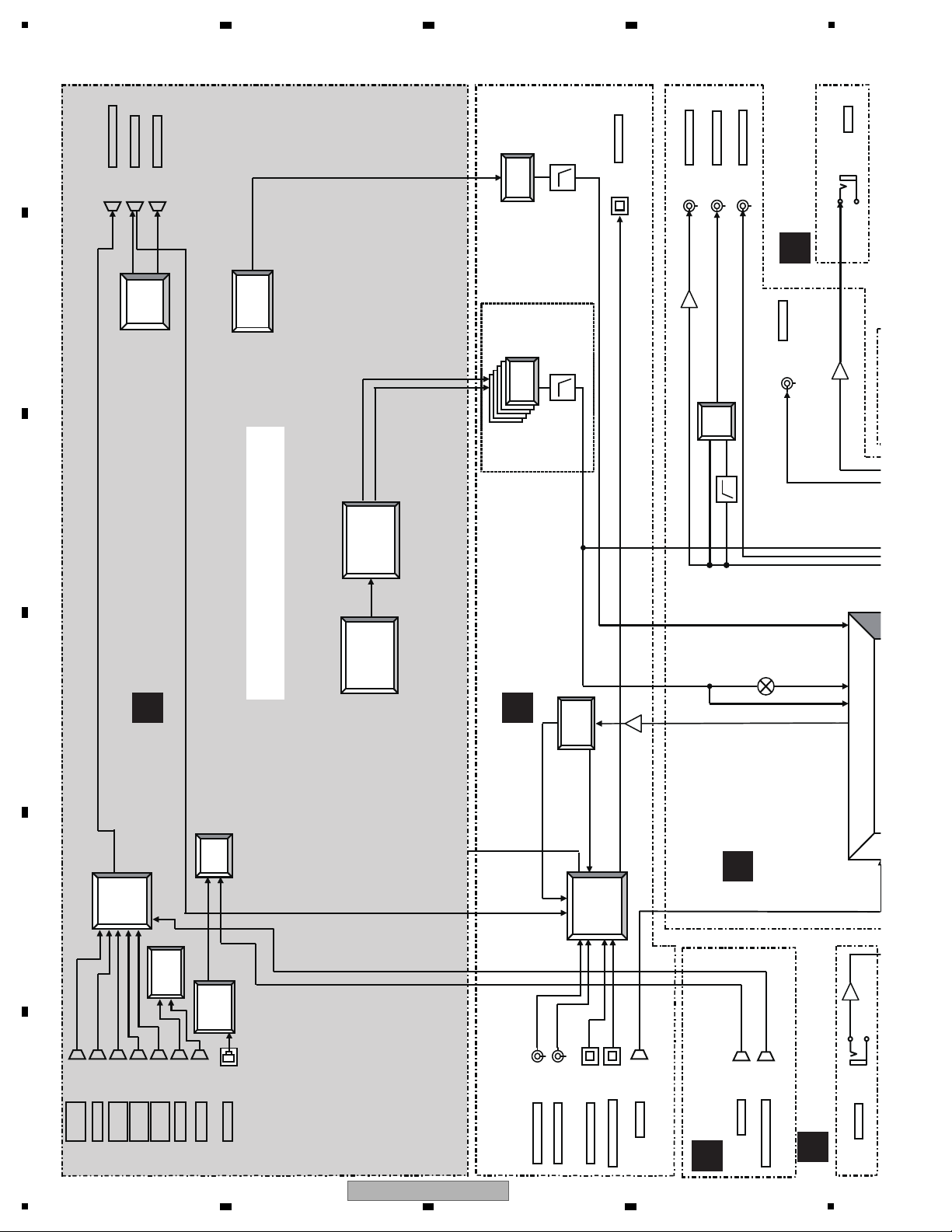
• SC-67
COAX2(SAT/CBL)
OPT IN1(TV)
OPT IN2(DVR/BDR)
COAX1(DVD)
DAC
AK4480EF
X5
TX1
LPF
JA2009
JA2010
JA2011
HDMI IN5(MHL IN)
MIC
DVR OUT
ZONE2 SW OUT
HP
SW DownMix
JA3471
JA8002
IC2701, IC2702
JA6701
JA2504
JA3476
ZONE3 OUT
JA6701
HEADPHONE
AMP
<<AUDIO ZONE OUT>>
MIC Amp
IC3471
NJM4565MD
IC2011(FL,FR)
IC2012(C,SW)
IC2013(SL,SR)
IC2014(SBL,SBR)
IC2017(FHL,FHR)
IC2003(FL,FR)
IC2005(C,SW)
IC2006(SL,SR)
IC2007(SBL,SBR)
IC2018(FHL,FHR)
IC2451
(ZONE2)
LPF
I2S
A/D BUFFER
IC2401,2402
NJM4565MD
USB
JA8001
OPT OUT1
IC2801
NJM4565MD
JA2008
IC2001
DIR&DIT
AK4118AEQ
IC2501
IC2431
ADC
PCM1804DB
I2S(DATA)
I2S(BCK,LRCK)
(SBL,SBR)
(FL,FR,C,SW,SL,SR,FHL,FHR)
IC9204
MNP
DM860A
IC9602
HDMI PORT
PROCESSER
SII9575CTUC
HDMI IN4
(VIDEO)
HDMI IN6
IC903
HDMI RX
SII9233ACTU
HDMI OUT1
IC9002
1st DSP
D808K013CPTP400
IC1609
HDMI
TRANSMITTER
SII9573CTUC
JA9603
JA9604
JA1601
HDMI IN7
JA9608
JA1602
HDMI OUT2
NETWORK
JA9202
IC9203
ETHERNET
PHYCEIVER
LAN8700C-AEZG
I2S(FL,FR)
IC1814
ZONE2
USB/NET
SELECTOR
BD
JA9601
I2S(except FL,FR)
BT
HDMI IN3
(DVR/BDR)
JA9602
HDMI IN2
(SAT/CBL)
JA9607
JA2102
IC9702
2nd DSP
D808K013CPTP400
ZONE2
ZONE2 OUT
JA6701
ZONE2 SW Amp
IC6701
NJM4565MD
IC6703
ZONE2
SELECTOR
IC6702
HPF
IC2471
ZONE2 DAC
AK4388ET
HDMI IN1
(DVD)
JA9606
HDMI ZONE4 OUT
JA1603
Refer to the “4-4 BLOCK DIAGRAM FOR
DIGITAL MAIN AUDIO BLOCK”
A
B
C
G
K
AUDIO ASSY
DAC HIGH ASSY
FRONT HDMI
USB ASSY
DIGITAL MAIN ASSY
MIC HP ASSY
K
MIC HP ASSY
A
1
2 3 4
B
C
D
E
F
18
1
SC-68
2 3 4
Page 19
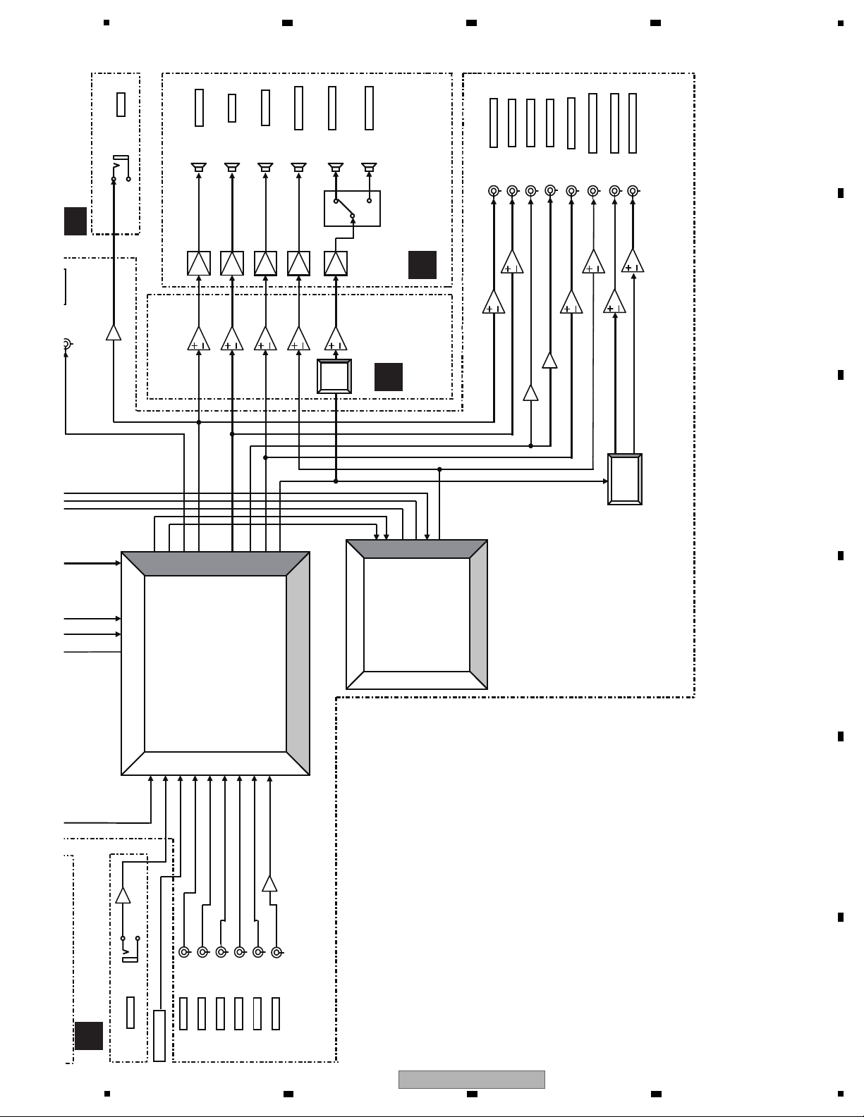
5
MIC
TV/SAT
VIDEO
CD
PREOUT FL/FR
PREOUT SW1
PREOUT SL/SR
PREOUT SBL/SBR
DVR OUT
SP FL/FR
SP C
SP SL/SR
SP SBL/SBR
HP
SW DownMix
JA3471
IC2701, IC2702
JA2502
JA2504
SW PRE Amp
IC2751
<<POWER AMP>>
JA2504
JA3476
JA4101
JA4101
JA4301
JA4501
JA3101
JA3101
JA3201
JA3201
PREOUT C
JA3101
DVD
DVR
JA2501
JA2501
HEADPHONE
AMP
<<POWER AMP
INPUT BUFFER>>
IC6821,
IC6841
IC6801
IC6861,
IC6881
IC6901,
IC6921
<<PREOUT>>
MIC Amp
IC3471
NJM4565MD
NJM4565MD
IC2801
NJM4565MD
JA2505
PREOUT FHL/FHR
JA3201
IC3221
PRE SELECTOR
SP FHL/FHR
JA4901
RY4500,RY5000
TUNER Module
IC3271
IC2501
Selector / Volume / PRE Amp
BD3473KS2
IC7491
L/R
SELECTOR
SW PRE Amp
IC2751
NJM4565MD
JA3102
PREOUT SW2
PREOUT FWL/FWR
JA3202
IC3272
IC3273
Selector / Volume / PRE
Amp
BD3473KS2
IC7451,
IC7471
SP FWL/FWR
JA5101
ZONE2
ZONE3
ZONE2
ZONE3
IC3101
IC3151
IC3201
IC3251
PHONO
JA2503
EQ Amp
IC2661
NJM4565MD
K
P
S
MIC HP ASSY
IR BUFFER
ASSY
D AMP ASSY
K
MIC HP ASSY
6 7 8
A
B
C
D
E
5
SC-68
6 7 8
F
19
Page 20
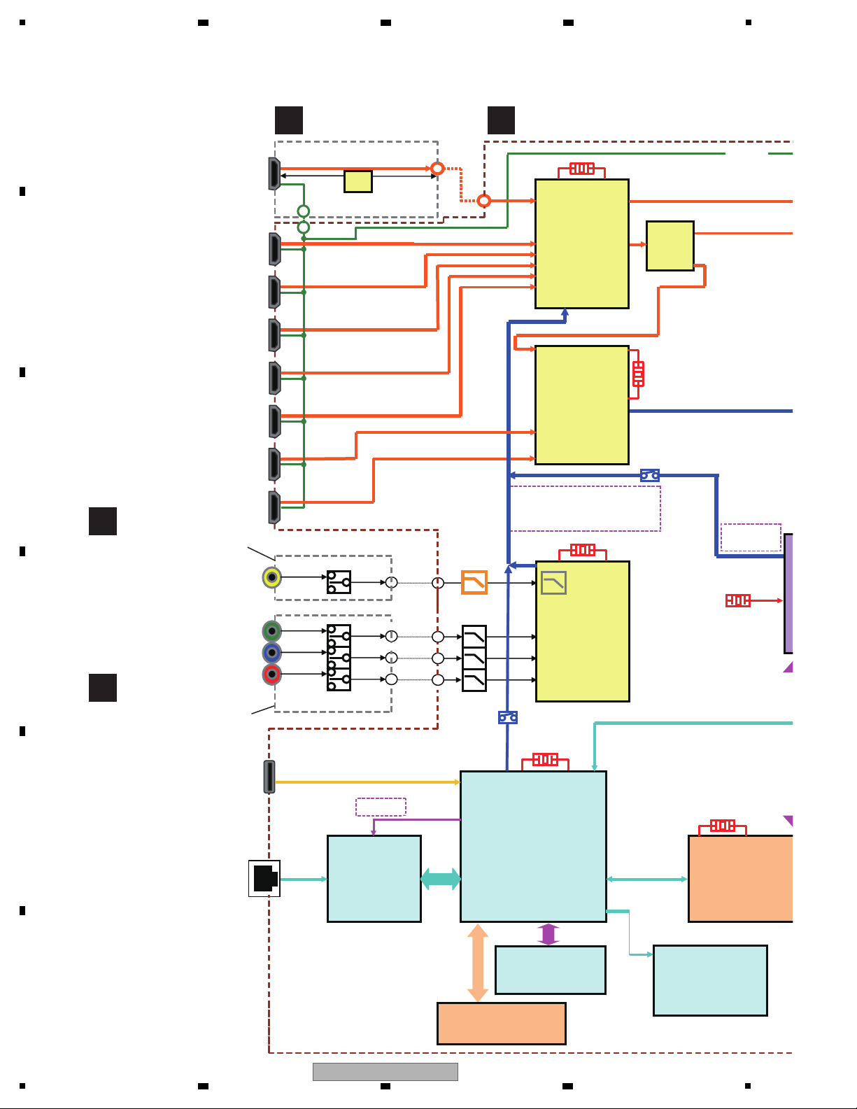
1
HDMI Rx
Silicon Image
"SiI9233"
PortProcessor
SiliconImage
"SiI9575"
Video Decoder
Analog
Devices
"ADV7181C"
Gate Array
SEIKO EPSO
"PE7008A"
LAN PHY
SMCS
"LAN8700"
Media Processor
BRIDGE CO
"DM860A"
SDRAM-166
256Mb(16Mx16)
FLASH ROM
1Gb
iPod
Authentication IC
"341S2162"
36.864MHz
28.63636MHz
27MHz
HDMI IN6
HDMI IN3
HDMI BDIN
HDMI IN1
HDMI IN2
HDMI
/IN5
/MHL
DDC
Buffer
COMPOSITE
COMPONENT
Pb
Pr
ETHERNET
More than VDEC 480p output
CK:27MHz-74.25MHz
/DT:16bit/DE,VS,HS
Y
24MHz
25MHz
HDMI IN7
CK:27MHz
/DT:BT656
BT
HDMI
SW
27MHz
HDMI IN4
27MHz
I
IC9602
IC903
IC603
IC9206
IC9204
IC9205
IC9201
IC9203
IC909
IC9603
CEC
C
FRONT HDMI
USB ASSY
G
DIGITAL MAIN ASSY
I
J
COMPONENT ASSY
COMPOSITE ASSY
2 3 4
4.3 BLOCK DIAGRAM FOR DIGITAL MAIN VIDEO BLOCK
A
B
C
D
E
F
20
1
SC-68
2 3 4
Page 21
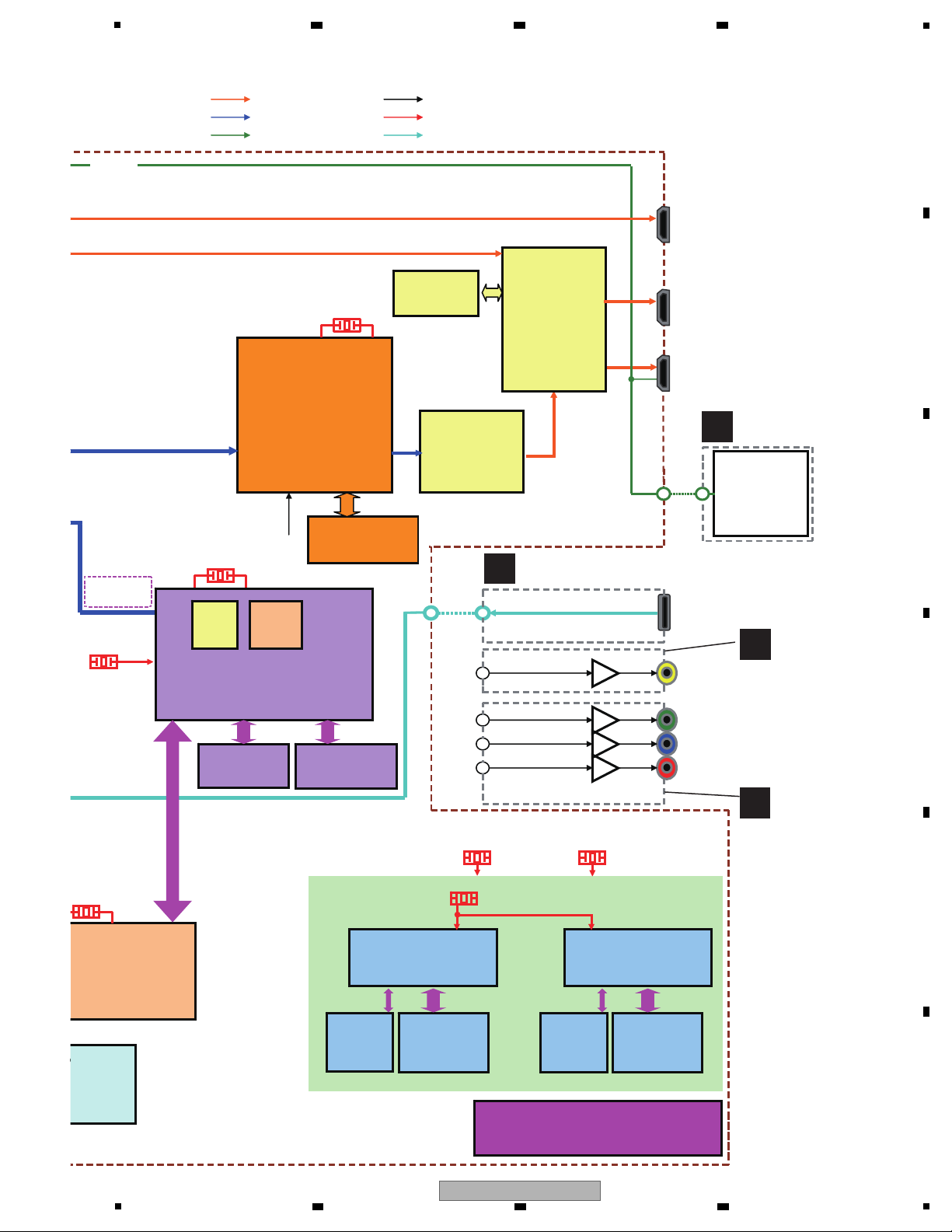
5
IP.SCALER
Marvell
"88DE2750"
EVENT ucom
SANYO
"LC87F5NC8A"
(PDC203A8)
IC3001
SDRAM
256Mb
Gate Array
SEIKO EPSON
"PE7008A"
cation IC
2
2
2
2
COMPONENT-Y
COMPOSITE
COMPONENT-Pb
COMPONENT-Pr
USB(FRONT)
HDMI OUT1
22.5792MHz
TMDS
DIGITAL VIDEO
CEC
ANALOG VIDEO
CLOCK
DIGITAL AUDIO
DDR2
512Mb
I2C
24.576MHz
20MHz
2nd DSP
D808K013CPTP400
SDRAM-166
64Mb(8Mx16)
SeriFlash
16Mb
20MHz
CK:27MHz
/DT:BT656
20MHz
PortProcessor
SiliconImage
"SiI9573"
HDMI Tx
Silicon Image
"SiI9136"
"EMMA2LL"
uCOMGUI
1st DSP
D808K013CPTP400
SDRAM-166
64Mb(8Mx16)
SeriFlash
16Mb
Nor FLASH
64Mb
27MHz
HDMI OUT2
SeriFlash
4Mb
IC101
IC1204
IC1212
IC1602
IC1609
IC1612
IC102IC103
IC9002 IC9702
IC9004
IC9001
IC9701
IC9703
27MHz
CEC
HDMI zone
L
DISPLAY ASSY
C
FRONT HDMI USB ASSY
I
J
COMPONENT
ASSY
COMPOSITE
ASSY
POWER SUPPLY BLOCK Diagram
(DCDC,LDO)
6 7 8
A
B
C
D
5
6 7 8
SC-68
E
F
21
Page 22
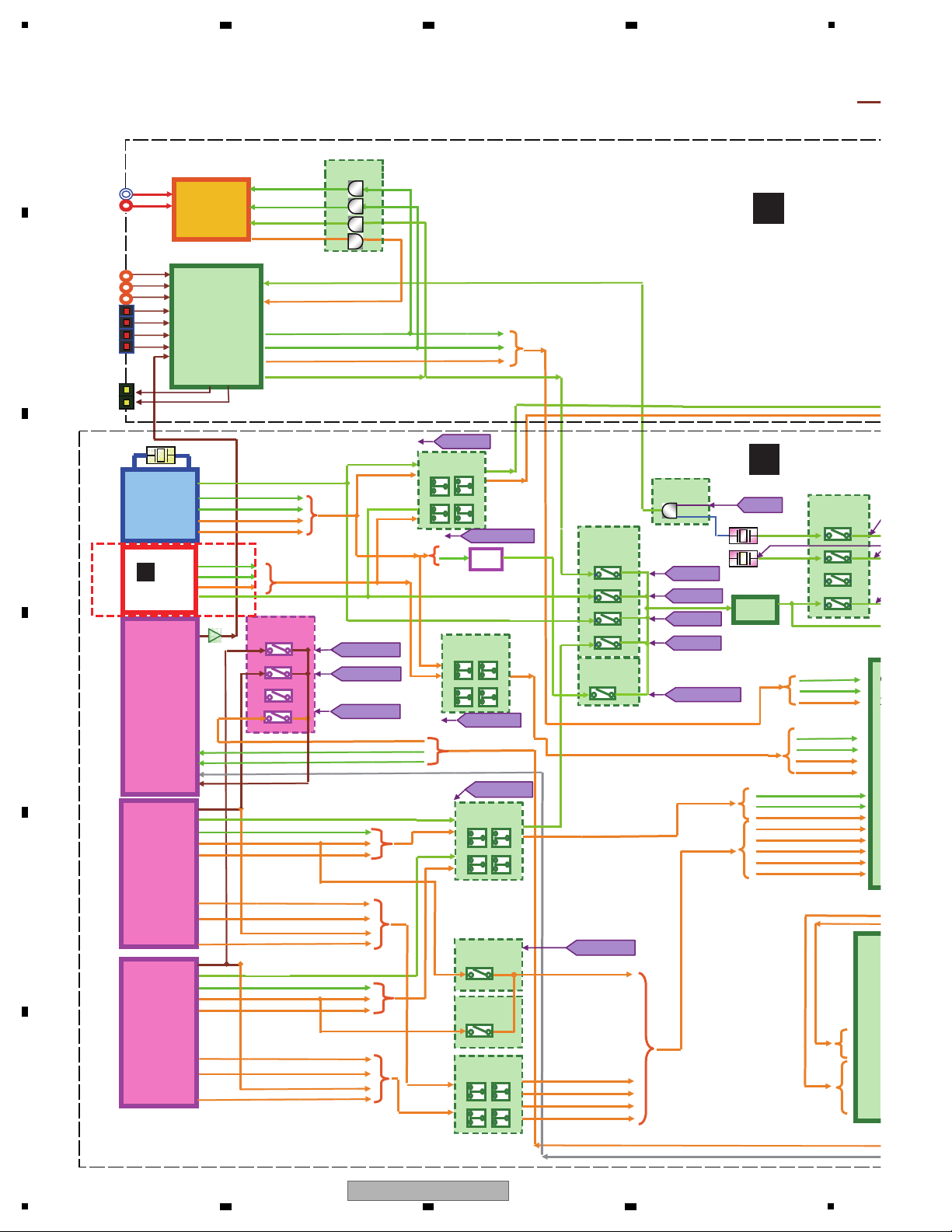
1
SEL
(VHC126)
IC1806
DIR
HDMI
Port
Processor
in
COAX 1
COAX 2
OPT 1
OPT 2
ADC
XTI
MCKO1
BCK2
LRCK2
SDTO2
DAUX
MSPDIF
COAX 3
OPT 3
OPT 4
AHCL
ACLK
AFSR
AXR0
AHCL
ACLK
AFSR
D1FD
D1CD
D1SD
D1BW
D1HW
D1DM
I2S DT(multi-ch)
SOURCE-I2S(LR)
24MHz
z
NMP
BCo
BCK
LRCK
FD/DSDFL
CD/DSDLFE
SD/DSDC
BD/DSDSR
DSDSL
DSDFR
HDMI
RX
HDMI
Port
Processor
out
AMCLK
BCK
LRCK/DSDFR
FD/DSDFL
SD/DSDC
CD/DSDLFE
BD/DSDSR
SPDIF/DSDSL
AMCLK
BCK
LRCK/DSDFR
FD/DSDFL
SD/DSDC
CD/DSDLFE
SPDIF/DSDSL
BD/DSDSR
SPDIF/DSDSL
SEL (LCX157)
IC1813
XHDI2SRX
SEL (LCX157)
IC1506
SEL (7SZ125)
IC1507
IC1508
DSDFR
SD/DSDC
CD/DSDLFE
SPDIF/DSDSL
BD/DSDSR
SEL
(VHCT126)
IC1613
HDSPDIFRX
HDSPDIFP
DSPI2S
I2S-DATA
I2S-BCK
I2S-LRCK
XHDI2SRX
AND (SZ08)
IC1804
XXTL0
ZDB
24.576MHz
22.5792MHz
SEL
(VHC126)
IC1509
HDMCK
DIRMCK
USBDMCK
NBCK
NLRCK
FD/DSDFL
DSDFR
BCK
LRCK
FD
SEL (LCX157)
IC1814
SEL (LCX157)
IC1501
NETMCK
ZNET
USBDMCK
AC
A
AX
A
A
A
A
A
A
A
A
A
A
A
A
A
A
NBCK
NLRCK
DSDFR
FD/DSDFL
IC1609
IC903
IC9602
AND
(LCX08)
SEL (7SZ126)
IC9204
NBCK
×8
NETDSDMC
SC-68 only
USB DAC
ASSY
F
SEL
(7SZ126)
IC1512
NETDSDMC
B
G
DAC HIGH A
DIGITAL MA
2 3 4
4.4 BLOCK DIAGRAM FOR DIGITAL MAIN AUDIO BLOCK
A
B
C
D
E
F
22
1
SC-68
2 3 4
Page 23
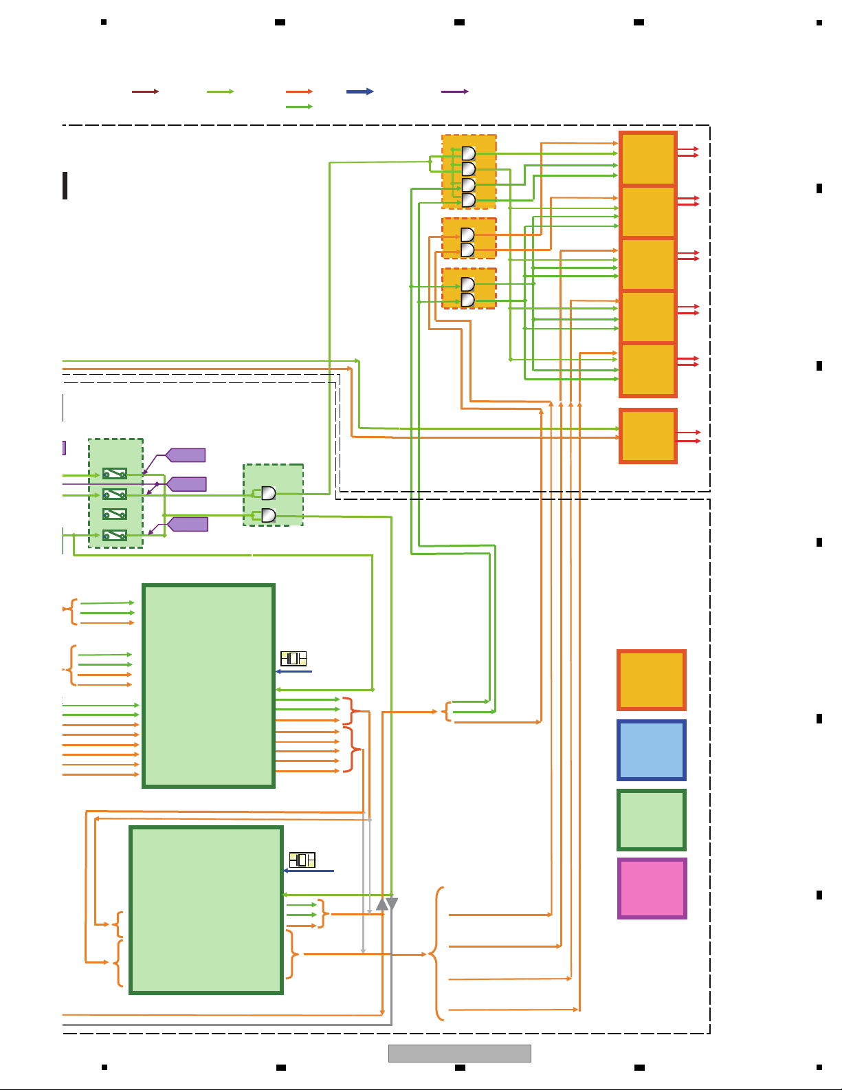
5
SEL
(VHC126)
IC1806
SPDIF
AMCLK
I2S
I2S-SURR
I2S-C/LFE
I2S-SRB/HEIGHT
I2S-FW/--
SYSCLK
ZONE-I2S (LR)
ZONE-AMCLK
20.0MHz
FLG
DAC
FL/FR
DAC
C/LFE
DAC
SL/SR
DAC
SBL/SBR
I2S-LR
I2S-C/LFE
I2S-SURR
I2S-SRB/
HEIGHT
Z2DAC
FL/FR
I2S-BCK
I2S-LRCK
I2S-LR
I2S-BCK
I2S-LRCK
I2S-DABCK
I2S-DALRCK
NETPOW
DIRPOW
DVCPOW
IC9702
2nd DSP
D808K013CPTP400
AHCLKR0
ACLKR0
AFSR0
AXR0[0]
AHCLKR1
ACLKR1
AFSR1
D1FDT AXR1[0]
D1CDT AXR1[1]
D1SDT AXR1[2]
D1BWDT AXR1[3]
D1HWDT AXR1[4]
D1DMDT AXR1[5]
DAC
FHL/FHR
RYAC
20.0MHz
K
SL
FR
IC9002
1st DSP
D808K013CPTP400
I2S BCK, LRCK
DAMCLK
AND (WZ08)
IC1802
Hz
24PQLS
22PQLS
DAZDB
NBCK
NLRCK
FD/DSDFL
DSDFR
BCK
LRCK
FD
AHCLKX0
ACLKX0
AFSX0
AXR0[7]D1FDT
AXR0[8]D1CDT
AXR0[9]D1SDT
AXR0[10]D1BWDT
AXR0[12]D1HWDT
AXR0[13]D1HWDT
AMUTE
AHCLKX0
ACLKX0
AFSX0
AXR0[7]D2FDT
AXR0[8]D2CDT
AXR0[9]D2SDT
AXR0[10]D2BWDT
AXR0[12]D2HWDT
AXR0[13]
AMUTE
ACLKR2
AFSR2
AXR2[0]
AHCLKR0
ACLKR0
AFSR0
AXR0[1]
AXR0[2]
AHCLKR1
ACLKR1
AFSR1
AXR1[0]
AXR1[1]
AXR1[2]
AXR1[3]
AXR1[4]
AXR1[5]
AND
(LCX08)
AND
(LCX08)
AND
(LCX08)
DAC HIGH ASSY
DIGITAL MAIN ASSY
6 7 8
A
B
C
5
6 7 8
SC-68
D
E
F
23
Page 24
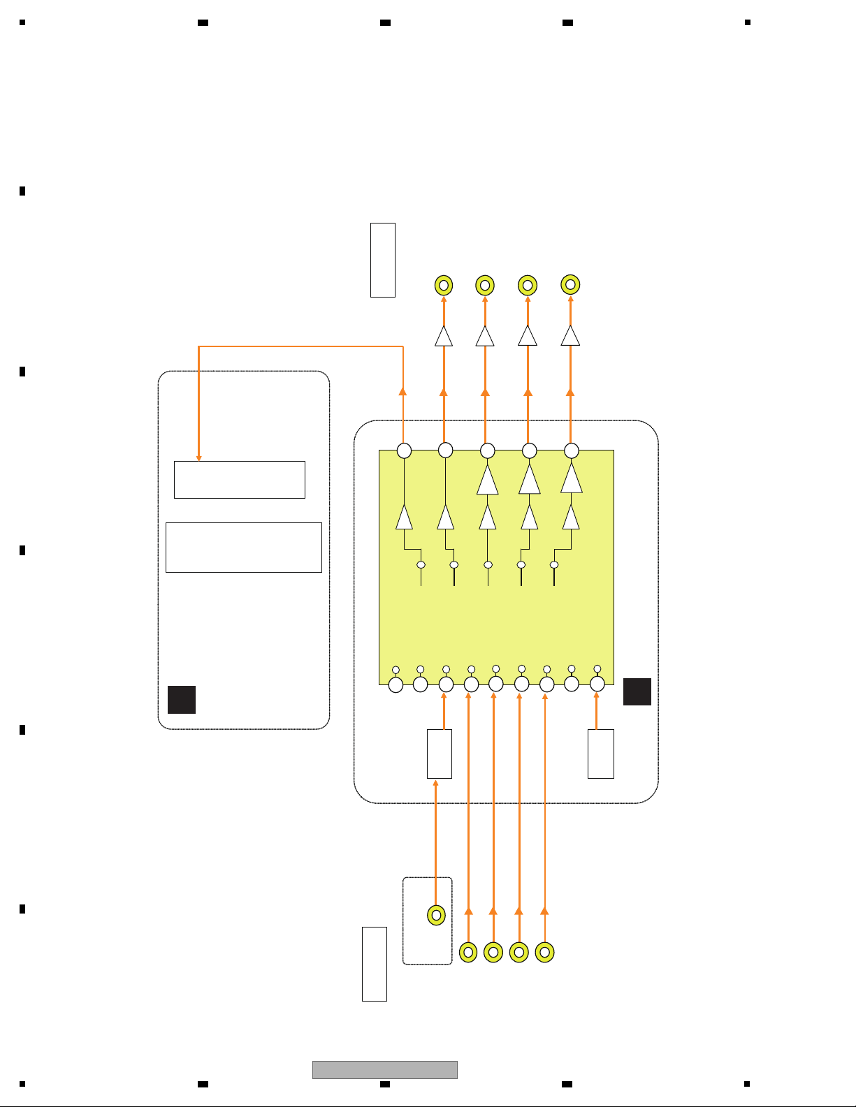
1
IC8301
IC8401
IC8501
EMMA
COMPOSITE
INPUT
COMPOSITE
OUTPUT
VDEC
OSD IC
PDC162A
FRONT VIDEO
DVD
TV/SAT
VIDEO
DVR/BDR
VIDEO AMP
NJM2505AF
iPod
ZONE3 OUT
ZONE2 OUT
MONITOR OUT
DVR/BDR OUT
95
94
93
92
91
89
88
87
83
82
81
79
77
75
75
75
VIDEO SW
NJW1327FU1
96
G
I
DIGITAL MAIN
ASSY
COMPONENT ASSY
2 3 4
4.5 BLOCK DIAGRAM FOR COMPOSITE VIDEO BLOCK
A
B
C
D
E
F
24
1
2 3 4
SC-68
Page 25
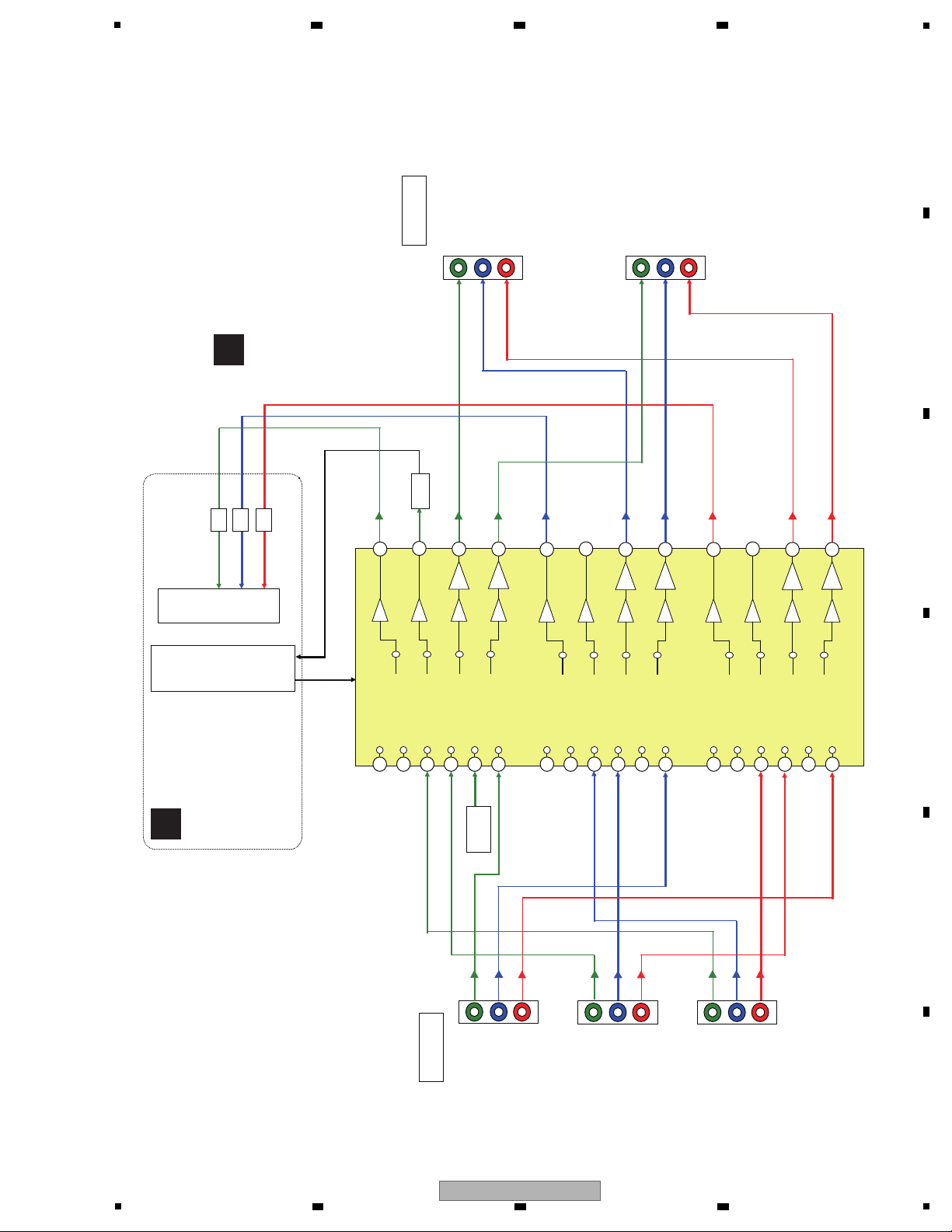
5
I2C
IC8301
IC8501
EMMA
IN 1
(DVD)
IN 3
(VIDEO)
IN 2
(DVR/BDR)
MONITOR OUT
ZONE 2 OUT
COMPONENT
INPUT
COMPONENT
OUTPUT
VDEC
LPF
LPF
LPF
CDET
VIDEO SW
NJW1327FU1
19
21
22
15
16
18
33
34
35
30
31
32
41
40
39
44
43
42
71
70
69
68
75
75
62
61
60
59
75
75
53
52
51
49
75
75
OSD IC
PDC162A
G
DIGITAL MAIN
ASSY
I
COMPONENT ASSY
6 7 8
4.6 BLOCK DIAGRAM FOR COMPONENT VIDEO BLOCK
A
B
C
D
E
5
6 7 8
SC-68
F
25
Page 26
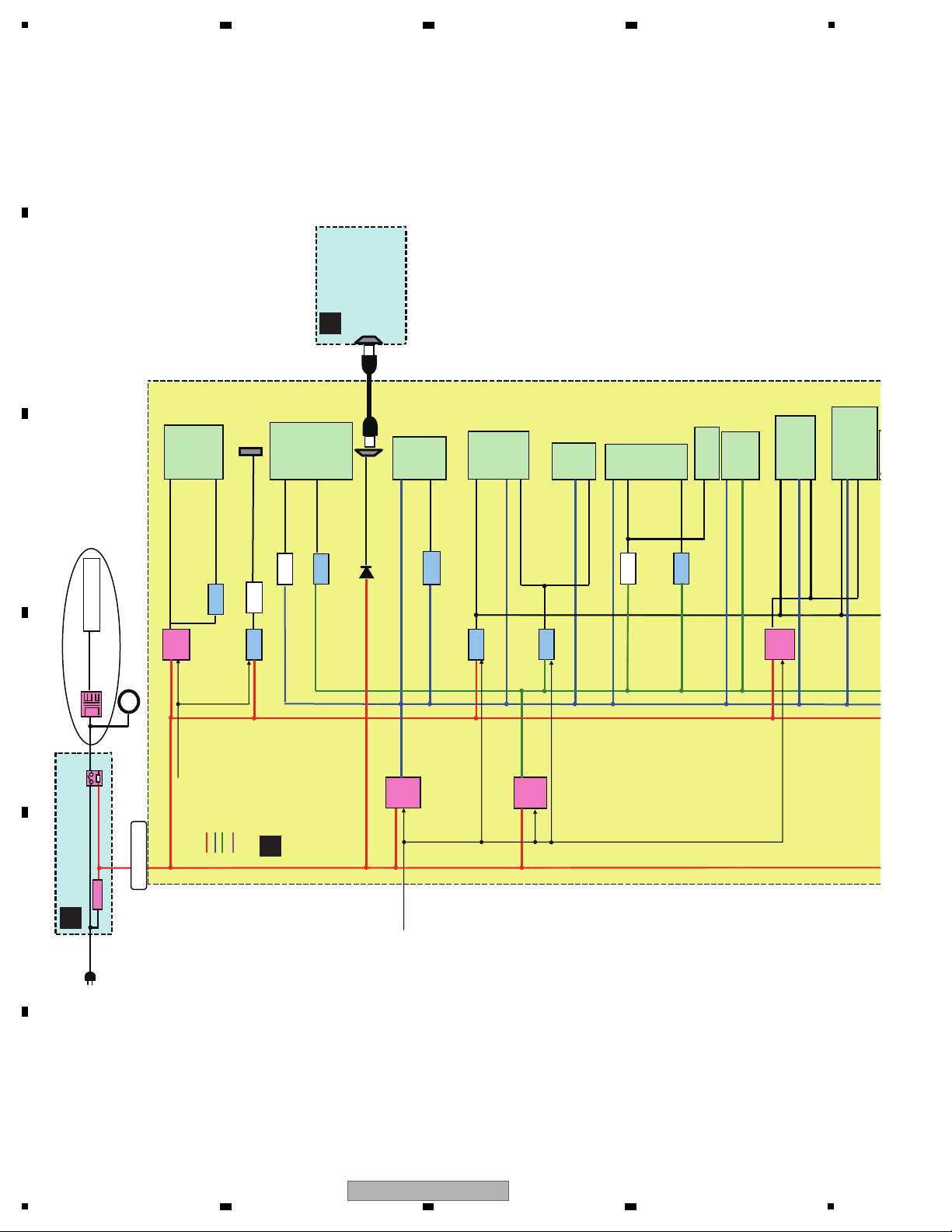
1
IC9521
BD9328
V+3R3_NW
NETPOW5
IC9502
S-1172B12
V+1R2_NW
IC9401 IC9202
S-1170B50 BD2226G JA9201
Q9507
RTQ040P02
V+3R3_EM
IC9515
S-1172B15
V+1R5_EM
V+5_EV JA9605
IC9520
BD9328
DVCPOW
IC9508
S-1170B25
V+2R5_EM
IC9511
S-1170B50
V+5_HD
IC9522
BD9329
V+1R2_HD
IC9523
S-1172B12
V+1R2_HD
V+1R8_SC
Q9503
RZQ0 45 P01
IC9501
S-1172B10
V+1R0_SC
IC9524
BD9328
V+5_HD
V+1R3_PP
V+5_HD
V+1R3_PP
SMPS
Other Circuits
V+5R6_EV
Refer to
MAIN Transformer part
IC9204
Network Media
Processor
DM860
A
1.2V
LDO
2.5V
LDO
IC903
HDMI Rx
SiI9233ACTU
IC1602
HDMI Tx
SiI9136CTU
IC603
Gate Array
PE7008A
IC9602
HDMI Port
Processor
SiI9575CTUC
1.8V
DCDC
Converter
3.3V
DCDC
Converter
IC101
Main Processor
EMMA2LL
IC102
SDR SDRAM
IC103
NOR FLASH
5V
LDO
3.3
DCDC
Converter
IC1204
Scaler
88DE2750
IC909
VideoDecoder
ADV7181CBSTZ
IC1212
DDR2 SDRAM
1.0V
LDO
FET SW
(1.8V)
5V
LDO
1.5V
LDO
IC1609
HDMI Port Processor
SiI9573CTUC
IC1612 Serial Flash
MX25L4006EM2I-12G
C
FET SW
(3.3V)
1.2V
LDO
1.3V
DCDC
Converter
V+3R3_H H H
V+5R 6_E V(D DD )
V+1R 8_H H H
V+3R3_D S P
5V
LOAD SW
+5V for
Wireless LAN
Converter
C N 9501
D9504
JA8003
A
C
G
T
FRONT HDMI
USB ASSY
DIGITAL MAIN ASSY
PRIMARY ASSY
2 3 4
4.7 BLOCK DIAGRAM FOR POWER BLOCK (1)
A
B
C
D
E
F
26
SC-68
1
2 3 4
Page 27
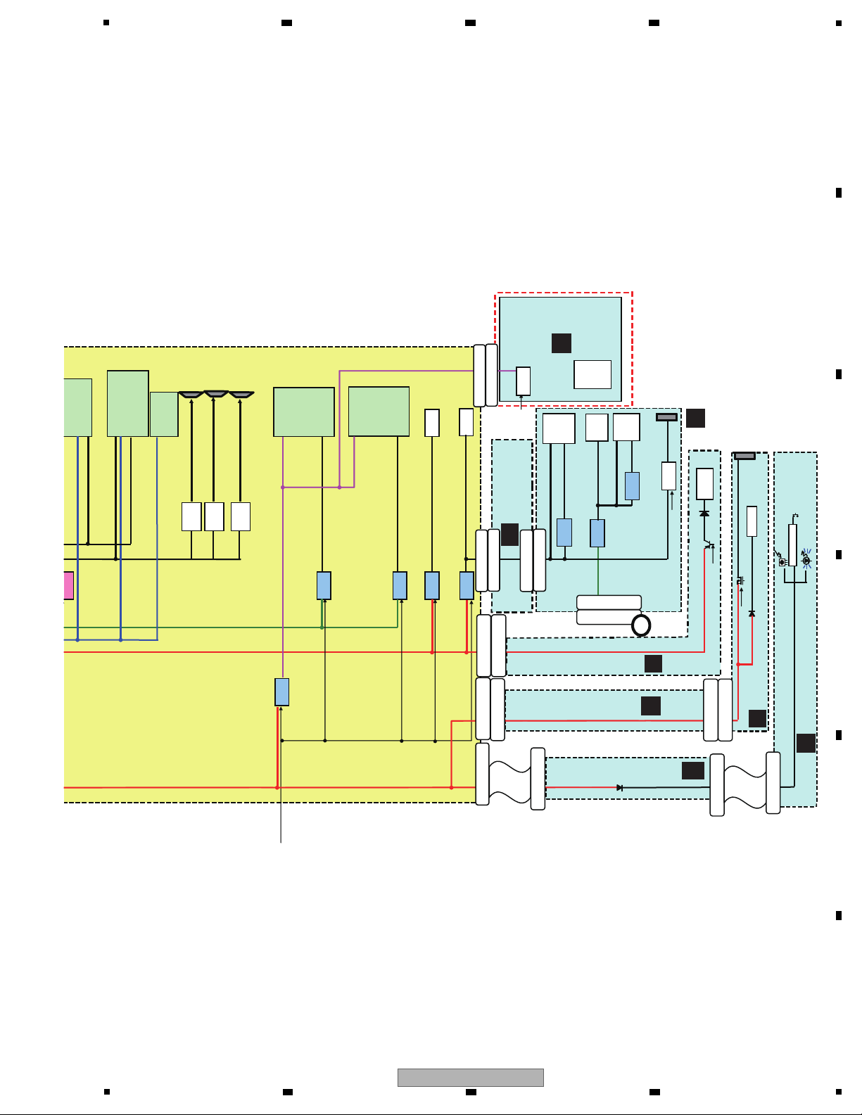
V+1R3_PP
V+5_HD
V+1R3_PP
AAT4610BIGV-1
+5V
+5V
+5V
IC9510
NJM2846DL3-33
DIRPOW
IC9518
S-1172B12
V+1R2_D1
IC9514
S-1172B12
V+1R2_D2
IC9512
NJM2872BF33
X1801,1802
V+3R3_OS
IC9504
S-1170B50
V+5_DSP
V+5_D
V+3R3_D
NJM2872BF33
V+5_D
JA2102
BT Connector
JA7002
HDMI Port
Processor
SiI9575CTUC
XTAL
Logic IC
5V
LDO
3.3V
LDO
IC9702
2ndDSP
D808K013CPTP400
IC9701
SDR SDRAM
1.2V
LDO
5V
LOAD SW
IC1609
HDMI Port Processor
SiI9573CTUC
IC1612 Serial Flash
MX25L4006EM2I-12G
IC9603
HDMI SW
PI3HDMI2310
IC9002
1stD SP
D808K013CPTP400
IC9001
SDR SDRAM
1.2V
LDO
Converter
3.3V
LDO
V+3R3_D SP
5V
LOAD SW5VLOAD SW
JA1601
JA1602
JA1603
IC1605
IC1610
IC1615
HDMI OUT1
HDMI OUT2
HDMI OUT
ZONE4
C N 9002
C N 601
FFC
C N 7901
C
N
210
4
C N 2101
IC8601
RS232C
SR, IR
CN78 02
CN602
CN78 04
C N 7004
CN8301
CN901
CN3784
CN3783
232POW
232POW
SC-68 ONLY
USB
DACP
ON
C N 5501
CN98 01
FET SW
(1.8V)
Q5622
RTQ040P02
IC5503
USBDAC
CM66 31
U SBDAC ASSY
Power Supply for
RF Remote/Extention
EVENT CPU
V+5_EV
IC3001
V+5_EV V+5R6_EV
C N 7902
FFC
CN3001
C
N
379
1
C
IC2001
DIR +
Peripheral
AK4118AEQ
IC2***
DAC
AK4480EF
IC2431
A/D
Convertor
3.3V
LDO
5V
LDO
C N 2101
BTPOW
V+3R3_DA
IC2183
IC2181
V+5_DA
V+6_AD
5V
LOAD SW
3.3V
LDO
IC2015
NJM2845DL1-05
NJM2872BF33
H
I
L
INTERFACE ASSY
COMPONENT ASSY
DISPLAY ASSY
Y
B
CONNECT ASSY
DAC HIGH ASSY
F
USB DAC
ASSY
D-DAC BRIDGE
ASSY
AD
DISPLAY BRIDGE ASSY
AF
5
6 7 8
A
B
C
D
5
SC-68
6 7 8
E
F
27
Page 28
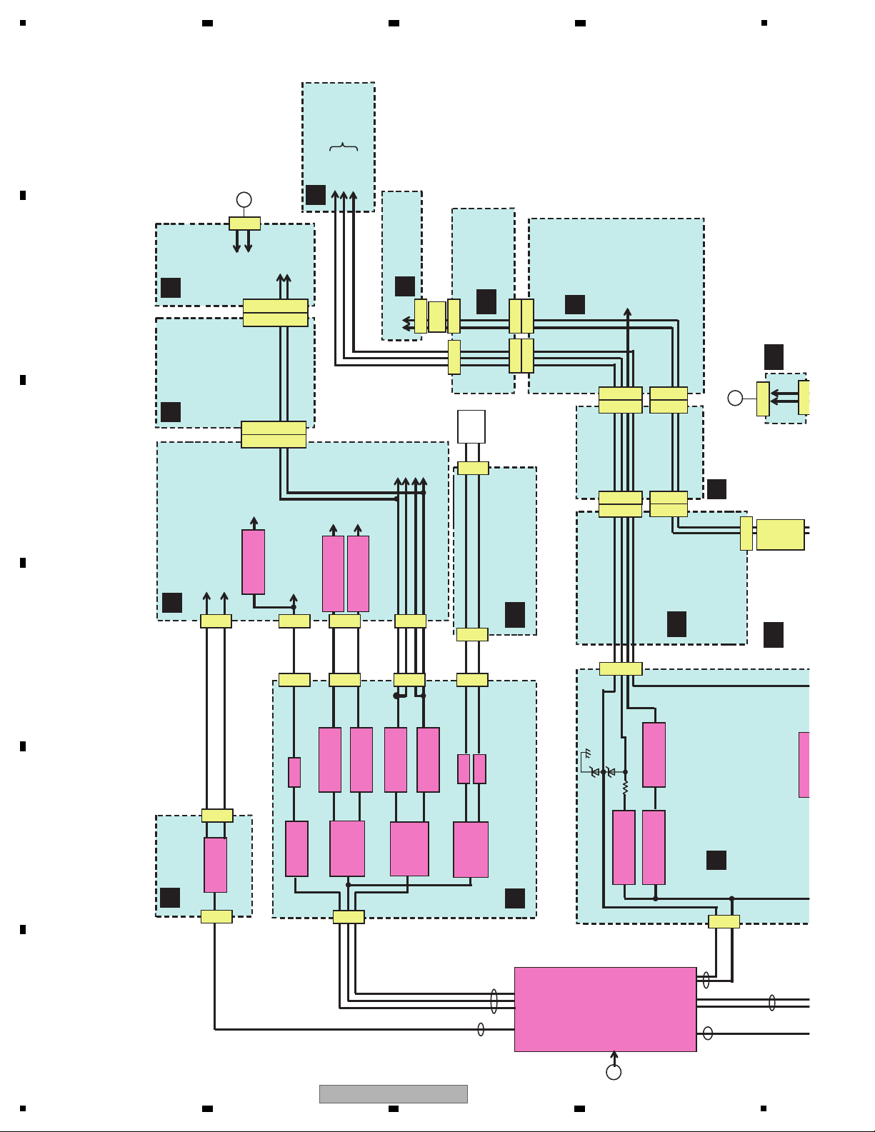
1
MAIN
Transformer
IC7521
RECTIFIER
D7621-7623,C7621
RECTIFIER
D7611-7613,C7611
IC7611
NJM78M12FA
5
CN7601
5
+
-
V+6AD
AC1,AC2
-VF
V+12TRG
2
for FL
FFC
A
CN7602
CN7721
CN7683
CN7681
CN7002
CN7724
CN7684
CN7722
CN7682
CN7007
CN7005 CN7008
CN7662 CN7661
CN7664
CN7663
FFC
CN3472
V-7_A
V+7_A
V+12TRG
AC1,AC2
-VF
V+5_V
RECTIFIER
D7241-7244
Q7241
RECTIFIER
D7271-7274
IC7271
NJM78M05FA
IC7272
NJM79M05FA
RECTIFIER
D7251-7254
IC7251
NJM78M12FA
IC7252
NJM79M12FA
Q7211
Q7212
CN7201
8
RECTIFIER
D7201-7204
+
+
+
+
-
-
-
CN7241CN7271CN7291
FAN
-B+15V
V+5_MD
V-5_MD
V+FAN
V-FAN
V+12DF
V-12DF
RECTIFIER
D7400,7401
3
CN7400
+
-
+B
-B
CN4001CN4002CN4003
V+64V
V-64V
VSS+12V
V+5V
V-5V
V+12V
V-12V
CN7251
CN4004
V+12RY
V-12RY
V+12**
V-12**
CN3801,3802
CN6802,6803
CN6801
CN3810-3890
CN4*00
CN6952
CN6951
B
B
V+7_A
V-7_A
CN7401
IC4*03
NJM2830U1-12
Driver IC VCC
CN5932
CN5931
H
Z
PR
S
W
V
INTERFACE
ASSY
FB-CONNECT
ASSY
IR BUFFER
ASSY
IR INTERFACE_M
ASSY
D AMP ASSY
IR REG ASSY
REG ASSY
AA
AK
PRE BRIDGE
ASSY
FAN CONNECT ASSY
X
B DIODE ASSY
A REG
BRIDGE
AI
AE
FRONT BRIDGE
ASSY
AG
F-IN BRIDGE
ASSY
L
DISPLAY ASSY
K
MIC HP ASSY
IC4008
NJM78M05DL1A
IC4009
NJM79M05DL1A
2 3 4
4.8 BLOCK DIAGRAM FOR POWER BLOCK (2)
A
B
C
D
SC-68
E
F
28
1
2 3 4
Page 29
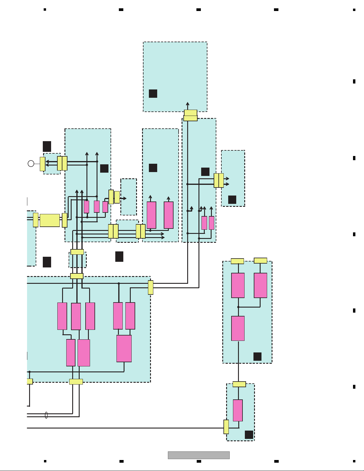
RECTIFIER
D7501-7504
IC7501
NJM78M12FA
IC7502
NJM79M12FA
IC7521
NJM78M06FA
RECTIFIER
D7601
IC7601
NJM78M05FA
IC7602
NJM79M05FA
5
CN7
+
-
+
-
V+12A
V-12A
V+6AD
V+5V
V-5V
CN7502
Q3001
Q3002
Q3901
V+12_A
V-12_A
TUNER MODULE
CN3902
FFC
V+5_T
V+7_A
V-7_A
V-12_A
V+12_A
V+5_DA
IC2181
NJM2855DL1-33
V+3R3_DA
Q8401
Q8402
V+5_V
V-5_V
V+3_V
V-3_V
V+5_V
V-5_V
CN8303
CN3601
CN3001
CN3792
CN3791
CN2104
FFC
CN8302
CN1722
V+5_V
RECTIFIER
D7521,7522
CN7501
+
CN7603
CN7724
CN2503
CN6952
CN3051
CN6951
B
CN5775
IC2183
NJM2845DL1-05
RECTIFIER
D3651
+
CN3651
V+5_USB
JA8001
USB +5V Supply
IC8004
BD9329EFJ
(DC-DC Conv.)
IC8001
TPS2557DRB
(Load SW)
V+UN_USB
JA8001
IC8002
STMPS2171T
(Load SW)
HDMI V+5MHL
Supply
CN3652
B
C
D
G
I
J
DAC HIGH ASSY
FRONT HDMI USB ASSY
USB RECT ASSY
DIGITAL MAIN
ASSY
COMPONENT ASSY
COMPOSITE ASSY
ASSY
REG ASSY
AA
PRE BRIDGE
ASSY
A-DAC
BRIDGE
ASSY
A
AUDIO ASSY
AB
A REG
BRIDGE
ASSY
AI
5
6 7 8
A
B
C
D
E
F
SC-68
5
6 7 8
29
Page 30
1
NO POWER
This is just for general reference and does not including every single case.
No Power
Error
Indications ?
Stand by
No
Yes
Yes
No
Refer to SM
"5.2 [4] Error Indications"
Other trouble.
FUSE FU4 OPEN ?
No
Yes
Diagnose or replace
PRIMARY ASSY
Check PRIMARY
ASSY JP51-1,2,3 pin
or DIGITAL MAIN
ASSY CN9501-1,2,3 pin
+5.6V
No
Yes
Check DIGITAL MAIN ASSY
CN601 -1,2 ,3 pin +5.6V
Check R872 on
DIGITAL MAIN ASSY
No No
Check +5.6V line on DIGITAL MAIN ASSY
or Replace DIGITAL MAIN ASSY
Yes
Check DISPLAY ASSY
CN3001-38,39 pin +5.6V
No
Replace FFC
(DISPLAY BRIDGE ASSY to DISPLAY ASSY)
Yes
Check DISPLAY ASSY
C3021 +3.3V
No
Replace DISPLAY ASSY
or replace D3008 or L3001
Yes
Check V-REG ASSY
CN7901-38,39 pin +5.6V
Replace FFC
(DIGITAL MAIN ASSY to DISPLAY BRIDGE ASSY)
No
Yes
Check V-REG ASSY
CN7902 -1,2 pin +5.6V
No
Replace DISPLAY BRIDGE ASSY
Yes
Check DISPLAY ASSY
X3001 oscillating
Check DISPLAY ASSY
L3001 +5V
No
Replace DISPLAY ASSY
or replace IC3003
Yes
No
Replace DISPLAY ASSY
Replace X3001
No
or
X3001 doesn't
oscilate
Replace IC3001
Yes
Check DISPLAY ASSY
IC3001 8 pin +5V
(XRESET)
No
Replace DISPLAY ASSY
or replace IC3002
Yes
Remove AC code and
remove CN9501. Insart
AC code and check
JP51-1,2,3 pin +5.6V?
Diagnose or replace
PRIMARY ASSY
No
Diagnose V+5R6_EV power supply
path after PRIMARY ASSY
Yes
A
2 3 4
5. DIAGNOSIS
5.1 DIAGNOSIS FLOWCHART
A
B
C
D
E
F
30
1
SC-68
2 3 4
Page 31

Diagnose or replace
DIGITAL MAIN ASSY
Check DISPLAY ASSY
IC3001 58 pin (POWKEY)
HL when press power key?
No
Check POWKEY signal path
Yes
Check DISPLAY ASSY
CN3001 27 pin (DVCPOW)
LH when press power key?
Check DVCPOW signal path
No
Yes
Check DISPLAY ASSY
CN3001 19 pin (ACRY)
LH when press power key?
No Problem
Replace DISPLAY ASSY
or replace IC3001
Check ACRY signal path
No
No Problem
Replace DISPLAY ASSY
or replace IC3001
Check PRIMARY ASSY
JP51 7 pin (ACRY)
LH when press power key?
Yes
Check ACRY signal path
DISPLAYDISPLAY BRIDGE
DIGITAL MAINPRIMARY ASSY
No
Does RY71 turn on
when press power key?
Yes
Check the circuits arround RY71
or replace PRIMARY ASSY
No
Yes
Check DIGITAL MAIN ASSY
CN601 13 pin (DVCPOW)
LH when press power key?
Check DVCPOW signal path
DISPLAYDISPLAY BRIDGE
DIGITAL MAIN ASSY
No
Yes
A
5
6 7 8
A
B
C
D
E
F
SC-68
5
6 7 8
31
Page 32

1
NO FL DISPLAY
This is just for general reference and does not including every single case.
No FL Display
Dimmer?
No
"FL OFF"LED
Light on?
Yes
No
JP3001 6-7 pin 4.3Vac?
Yes
No
V3301 1-62 pin 4.3Vac ?
No
V3301(FL Display) damage ?
Yes
No
Yes
Replace V3301
Check FL AC1, 2 power supply
path or replace DISPLAY ASSY
JP3001 5 pin -30V (VF)?
JP3001 4 pin +5V?
Diagnose REG ASSY
(arround IC7601,D7625)
or replace REG ASSY
No
Yes
Check the path of V+5_V,-VF
(Signal path is same as FL AC1 and 2)
All NG
All NG
Replace Transformer
Diagnose or replace
NG ASSY
Other results
Other results
Diagnose the circuits
(arround D3208)
or replace DISPLAY ASSY
Diagnose arround IC3201 or replace
DISPLAY ASSY
Check DISPLAY ASSY
X3201 oscillating
Yes
No
Replace X3201, IC3201 or DISPLAY
ASSY
Check the path of FL AC1 and 2
DISPLAY ASSY F-IN BRIDGE ASSY
INTERFACE ASSY FB-CONNECT
ASSY FRONT BRIDGE ASSY
REG ASSY MAIN TRANS
A
2 3 4
B
C
D
E
F
32
1
SC-68
2 3 4
Page 33

5
NO SOUND
This is just for general reference and does not including every single case.
No Sound
Head Phone
Speaker Front ch
Speaker
(Front ch is OK)
Pre OUT Front ch
Diagnose MIC HP ASSY
(arround JA3476)
or replace MIC HP ASSY
Yes
No
No
Analog in (e.g CD)
Pure Direct
Pre out sound
Yes
Check A-DAC BRIDGE ASSY
CN3794,3793 21,23 pin Signal
(FL OUT, FR OUT)
Diagnose AUDIO ASSY
Go to Flow [A]
Diagnose or replace
D AMP ASSY
No
No
No
Yes
No
No
Yes
Yes
Diagnose DAC HIGH ASSY
(DA part is NG)
Go to Flow [B]
Yes
Zone2 Audio no
output (MAIN is OK)
Analog inoutput
from Zone 2 line
Yes
No
Digital inoutput
from Zone 2 line out?
No
Yes
No
Check MIC HP ASSY
CN3472 1 or 3 pin (HP
OUTPUT SIGNAL)
Yes
No Problem /
No Damage
No
Diagnose AUDIO ASSY
(circuits arround IC2801)
or replace AUDIO ASSY
Analog Input
Digital Input
INPUT ?
Change to
"Auto Surround"
Pre OUT Front ch
A-DAC BRIDGE ASSY
CN3794,3793 25,27 pin Signal
D-DAC BRIDGE ASSY
CN3781 20,23,24,25 pin
Clock,Data
D-DAC BRIDGE ASSY
CN3781 3,9,10,12 pin Clock,Data
Diagnose or replace
DIGITAL MAIN ASSY
D-DAC BRIDGE ASSY
CN3781 5 pin Clock
Yes
Pre OUT Front ch
Signal
No
Yes
AUDIO ASSY
CN3051 10,14 pin Signal
Yes
No
Check the signal path of
FL OUT,FR OUT in AUDIO ASSY
or replace AUDIO ASSY
Pre OUT
(Front ch is OK)
A-DAC BRIDGE ASSY
CN3794,3793
5,7,9,11,13,15,17,19 pin Signal
Yes
No
D-DAC BRIDGE ASSY
CN3781 20,23,24,26,27,28 pin
Clock,Data
Yes
No
Pre OUT of C, SL, SR,
SBL, SBR, FHL or FHR
OK?
No
Yes
AUDIO ASSY
CN3051 2,4,6,8,12,16,18 pin
Signal
Yes
No
A-DAC BRIDGE ASSY
CN3794,3793 1,3 pin Signal
D-DAC BRIDGE ASSY
CN3781 14,15,16 ,18 pin
Clock, Data
Yes
No
Zone3 Audio no output
(MAIN is OK)
IR BUFFER ASSY
CN6803 1,6 pin Signal
Diagnose or replace
IR BUFFER ASSY
No
Yes
IR BUFFER ASSY
CN6802 3,8,13,18 pin,
CN6803 11,16,21 pin Signal
No
Yes
When headphone is
connected,speaker
relays turn off
(hear relay click sound)
Yes
No
Check MIC HP ASSY
CN3472 7 pin(XHPDET)
When headphone is
connected, + 3.3V 0V
Diagnose MIC HP ASSY
(arround Q3451)
or replace MIC HP ASSY
Check CONNECTORs and FFCs
MIC HPF-IN BRIDGEINTERFACE
FB-CONNECTFRONT BRIDGE
AUDIOD-AUDIO BRIDGE
DIGITAL MAIN ASSY
No Problem /
No Damage
No
Yes
Diagnose or replace
DIGITAL MAIN ASSY
Diagnose or replace
DIGITAL MAIN ASSY
Check the signal path of audio
output signals in AUDIO ASSY
or replace AUDIO ASSY
Diagnose or replace
D AMP ASSY
Diagnose or replace
IR BUFFER ASSY
Diagnose DAC HIGH
ASSY(AD or DIR part is NG)
Go to Flow [B]
Check the audio signal in AUDIO ASSY
[CN2502 5,7,9,11,13,15,17,19 pin
IC2501 or IC3273(IC3221)
IC2751,IC3151,IC3201,IC3251,IC3271,
IC3272Preout terminals]
or replace AUDIO ASSY
Check the audio signal in AUDIO ASSY
(Selected input terminalIC2501
CN2502 25,27 pin)
or replace AUDIO ASSY
Diagnose DAC HIGH ASSY
(DA part is NG) Go to Flow [B]
Check the audio signal in AUDIO ASSY
(CN2502 21,23 pin IC2702IC2501
IC3101JA3101)
or replace AUDIO ASSY
Check the audio signal in AUDIO ASSY
(IC2501 34,35 pin
JA6701 Zone 2 OUT terminal)
or replace AUDIO ASSY
Check the audio signal in AUDIO ASSY
(CN2502 1, 3 pin IC2501) or replace
AUDIO ASSY
Diagnose DAC HIGH ASSY
(DA part is NG) Go to Flow [B]
Diagnose or replace
DIGITAL MAIN ASSY
Check the audio signal in AUDIO ASSY
(IC2501 77,78 pin
JA3206 Zone 3 OUT terminal)
or replace AUDIO ASSY
Set"STEREO"mode with
STANDARD SURROUND key.
When speakers set ON/OFF
with SPEAKERs key, is INTER
FACE ASSY CN7006 9 pin
changed 0 5V ?
Yes
DIGITAL MAIN ASSYCN603
14 pin changed 0 5V?
Check IC612 11, 13 pin on
DIGITAL MAIN ASSY. If it is OK,
repalce DIGITAL MAIN ASSY
No
No
Yes
Check relay signal path between
INTERFACE ASSY and DIGITAL MAIN ASSY
Analog in (e.g CD)
Select EXT. STEREO
When speakers set ON/OFF with
SPEAKERs key, is INTERFACE
ASSY CN7006 6,7,8,10 pin
changed 05V?
Analog in (e.g CD)
Select EXT.
STEREO
Yes
Yes
DIGITAL MAIN ASSY CN602
2 pin, CN603 11, 12, 13 pin
No
Check relay ON/OFF signal at
IC612 and IC601 on DIGITAL MAIN ASSY.
If it is OK, repalce DIGITAL MAIN ASSY
No
Check relay signal path
between INTERFACE ASSY
and DIGITAL MAIN ASSY
Only iPodUSB and HMG
can be selected for zone 2
digital input.
BD,HDMI can't be selected.
It's specification.
Yes
Analog inoutput
from Zone 3 line
No
Yes
Digital inoutput
from Zone 3 line out?
No
Yes
Zone line out is OK, but speaker out NG.
Zone speaker out takes same signal path as
one of main channels.(It can be selected by
SP system setting.)
Refer to speaker (front is OK) flow.
Which channels correspond to zone, refer to
instruction manual.
Only iPodUSB and HMG
can be selected for zone 3
digital input.
BD,HDMI can't be selected.
It's specification.
C
C
changed 05V?
B
Check CONNECTORS and FFCs
MIC HPF-IN BRIDGE
INTERFACEFB-CONNECT
FRONT BRIDGEAUDIO ASSY
6 7 8
A
B
C
D
5
6 7 8
SC-68
E
F
33
Page 34

A
BT in
(Other Analog OK)
Tuner
(Other Analog OK )
USB in
(Other Digital OK)
Front HDMI in
Rec out no output
(PreOUT is OK)
Same input Function?
It is specification.
Yes
No
Rear HDMI inoutput
Diagnose FRONT HDMI USB ASSY
(arround IC8003) or replace
FRONT HDMI USB ASSY or HDMI
Cable from FRONT HDMI USB Assy
Yes
No
Check DIGITAL MAIN
ASSY CN9202
2,3 pin Digital Signal
Diagnose FRONT HDMI USB ASSY
(arround IC8001,IC8004,JA8001,CN8001)
or replace FRONT HDMI USB ASSY
Diagnose or replace
DIGITAL MAIN ASSY
AUDIO ASSY CN3902
7,9 pin Signal
AUDIO ASSY CN3902
8 pin +5V
Yes
No
Yes
Replace TUNER MODULE
No
A-DAC BRIDGE ASSY
CN3792 12,14 pin Signal
Yes
No
Diagnose DAC HIGH ASSY
(arround IC2473,
audio signal JA 2102 CN 2104)
or replace DAC HIGH ASSY
FRONT HDMI USB ASSY
JP8001 1 pin +13V
Yes
No
USB RECT ASSY
FU10 Open
Replace FU10
Yes
No
Repair or replace
USB RECT ASSY
Yes
No
MEDIA SERVER in
(Other Digital OK)
Check the audio signal in AUDIO ASSY
(IC2501 71,72 pinJA2504 DVR OUT terminal)
or replace AUDIO ASSY
Check the audio signal in AUDIO ASSY
(CN3902 7,9 pinIC2501)
or replace AUDIO ASSY
Diagnose AUDIO ASSY
(circuits arround Q3901)
or replace AUDIO ASSY
Check the audio signal in AUDIO ASSY
(CN3001 12,14 pinIC 2501 )
or replace AUDIO ASSY
Diagnose or replace
DIGITAL MAIN ASSY
Diagnose DIGITAL MAIN ASSY
(arround IC9204,IC9203)
or replace DIGITAL MAIN ASSY
Phono in
(Other Analog OK)
Diagnose AUDIO ASSY
(circuits arround IC2661)
or replace AUDIO ASSY
USB DAC in
(Other Digital OK)
Diagnose USB DAC ASSY
(arround IC5503,IC5512,X5501,X5502,
X5503) or replace USB DAC ASSY
Diagnose or replace
DIGITAL MAIN ASSY
No
MHL in
(Front HDMI in OK)
Diagnose FRONT HDMI
USB ASSY
arround Q8014 - Q8016
Replace FRONT HDMI
USB ASSY
Cable or Source
device confirm
No
Yes
SC-68 only
B
B
1
2 3 4
C
D
E
F
34
1
2 3 4
SC-68
Page 35

Flow [A]
AUDIO ASSY diagnostic
AUDIO ASSY
JP3001 2,5 pin ±12V
No
Check ±12V power supply path
REG
A REG BRIDGEAUDIO ASSY
ALL NG
Other results
Repair or replace NG point
Diagnose REG ASSY
(arround IC7501,IC7502)
or replace REG ASSY
AUDIO ASSY
CN2861 11,12,13 pin
Clock,Data
when master volume is
changed
Yes
Diagnose or replace
DIGITAL MAIN ASSY
No
Yes
Continue the following flow or
replace AUDIO ASSY
AUDIO ASSY
C3025,3026 ± 7V
No
Diagnose the circuits
arround Q3001,Q3002
AUDIO ASSY
Check IC2501,IC3273
power supply pins
(13 pin:+7V, 9 pin: -7V)
Yes
NG
Check the power supply path
AUDIO ASSY
Check IC2501,IC3273
clock(10 pin), data pins(11 pin)
OK
OK
NG
Check the clock, data signal path
Input the analog audio signal,
set to "Pure Direct",
Check the analog signal path
IN:OK,OUT:NG
at IC2501
Replace IC2501
Other results
Dignose and repair NG point
e.g. if selecting "CD", check
INL11 58 pin / INR11 57 pin,
outputs is FROUT 8 pin / FLOUT 7 pin
5
6 7 8
A
B
C
D
E
F
SC-68
5
6 7 8
35
Page 36

A
Flow [B]
DAC HIGH ASSY
diagnostic
DAC HIGH ASSY
CN2104 9,10 pin +6V
Check +6V power supply path
REG
A REG BRIDGEAUDIO
A-DAC BRIDGEDAC HIGH ASSY
No
ALL NG
Other results
Repair or replace NG point
Diagnose REG ASSY
(arround IC7521)
or replace REG ASSY
DAC HIGH ASSY
CN2101 18,19 pin +5V
Yes
No
Yes
Check +5V power supply path
DIGITAL MAIN
D-DAC BRIDGE
DAC HIGH ASSY
ALL NG
Other results
Repair or replace NG point
Diagnose DIGITAL MAIN ASSY
(arround IC9504)
or replace DIGITAL MAIN ASSY
Yes
DAC HIGH ASSY
Check the control signals
CN2101
15 pin DSPCK
16 pin DSPSO
10 pin DACS
3 pin DIRCS
When function is changed,
do clock,data,cs signals come?
Diagnose or replace
DIGITAL MAIN ASSY
No
Yes
Continue the following flow or
replace DAC HIGH ASSY
Diagnose NG part of
DAC HIGH ASSY
DA part (MAIN)
around IC2011-2014,2017
DA part (zone 2)
arround IC2471
AD part
arround IC2431
DIR part
arround IC2001
B
1
2 3 4
C
D
E
F
36
1
2 3 4
SC-68
Page 37

5
NO PICTURE
This is just for general reference and does not including every single case.
No Picure
Composite in
Composite out or
zone 2 Video out
Component in
Component out or
zone 2 Component out?
HDMI inHDMI out?
Composite
(Component) in
HDMI out?
GUI?
iPod Video in
Composite out?
Rear Composite in
Composite out
Yes
No
Diagnose or replace
MIC HP ASSY
Diagnose or replace
DIGITAL MAIN ASSY
HDMI in
HDMI Zone4 out?
Diagnose or replace
DIGITAL MAIN ASSY
Check MIC HP ASSY
MIC CONNECT ASSY
COMPONENT ASSY
conection
No Problem
Problem
Replace or repair
problem point
Analog Video IN?
Check
COMPONENT ASSY
CN8303 Video signals
IN:OK,OUT:NG
IN:NG,OUT:NG
Diagnose COMPONENT ASSY
(arround IC8301)
or replace COMPONENT ASSY
Diagnose COMPOSITE ASSY
(input circuits)
or replace COMPOSITE ASSY
IN:OK,OUT:OK
Diagnose COMPOSITE ASSY
(output circuits)
or replace COMPOSITE ASSY
Diagnose or replace
DIGITAL MAIN ASSY
Diagnose or replace
DIGITAL MAIN ASSY
6 7 8
A
B
C
D
E
F
SC-68
5
6 7 8
37
Page 38

1
This is just for general reference and does not including every single case.
12V Trig
RS-232C
RF Remote
IR/SR
12VTrig
IR/SR
RS-232C
Check INTERFACE ASSY
CN7002 4pin +12V
No
Remote Control
Check the signal path of
IR-IN,SR-IN,RMC
INTERFACE
CONNECT
DIGITAL MAINDISPLAY
BRIDGE
DISPLAY ASSY
No
Yes
Diagnose COMPONENT ASSY
(arround IC8601)
or replace COMPONENT ASSY
No
Diagnose INTERFACE ASSY
(IR,SR circuits)
or replace INTERFACE ASSY
RF Remote
No
INTERFACE ASSY
JA7002 1pin +5V
Yes
Check INTERFACE ASSY
C7108 +5.6V
No
Is 232C OK?
NG
OK
It's problem of the RF
Receiver Box or RF
Remote Controler
No
Diagnose INTERFACE ASSY
(Circuits arround Q7008,Q7010)
or replace INTERFACE ASSY
Yes
No
ALL NG
Other results
Repair or replace
NG point
Diagnose REG ASSY
(Circuits arround IC7551)
or replace REG ASSY
Still NG
Check the signal path of 232RX,232TX
COMPONENT
DIGITAL MAINREG-
DISPLAY ASSY (IC3001 )
and check the power supply path of V+5R6_EV
PRIMARY
DIGITAL MAINCOMPONENT ASSY
No
Diagnose INTERFACE ASSY
(circuits arround Q7022)
or replace INTERFACE ASSY
Yes
Check the power supply of V+5R6_EV
PRIMARY
DIGITAL MAINCONNECT
INTERFACE ASSY
NG
Repair or replace
NG point
No problem
Diagnose DISPLAY ASSY
(IR,SR,RMC signal path,
arround U3201)
or replace DISPLAY ASSY
OTHER
Check V+12_TRG power supply path
REGFRONT BRIDGE
FB-CONNECTINTERFACE ASSY
A
2 3 4
B
C
D
E
F
38
SC-68
1
2 3 4
Page 39

5
[1] Protection Circuit Process List
Amplifier Circuit
Item Purpose Detection Method Status of Equipment Warning Indication Remarks
Overheat
detection
Detects MOS FET
temperature of amplifier output
stage
Detects when TEMPERR PORT
becomes "L" in case of the
detecting temperature exceeds
95°C or rapid change by short
cuicuit of speaker terminals.
(IC3001 72pin)
Blinks FL OFF LED
indicator.
Recoverable by power-on
after shutdown in one
minute.
MAXTEMP voltage
5V-1.8V : FANLOW
1.8V or less : FANHIGH
Detects when MAXTEMP port
becomes below 1.9V at NTC
Thermistor detect circuit.
(IC3001 2pin)
Fan rotates by power-on.
DC
detection
Detects DC of amplifier output
(After LPF)
Detects when SP output exceeds
DC ± 7V and DCERR port
becomes "L". (IC3001 80pin)
MUTE on and Speaker
Relay off.
Flashes “AMP ERR”.
Shuts down when
abnormality continues for
more than 3 seconds.
MUTE on and Speaker
Relay off.
Flashes “AMP ERR”.
Shuts down when
abnormality continues for
more than 3 seconds.
Blinks ADVANCED
MCACC LED
Blinks FL OFF LED
indicator.
In case of detecting DC
abnormality during normal
operation. Recoverable by
power-on after 1 minute.
In case of detecting DC
abnormality during
power-on sequence after
the DC was once detected.
Recoverab
le by only DC
DETECT cancel.
Refer to “How to Enter
Release Mode” .
Fan
abnormality
detection
Detects a Fan not rotating by
loose connector or Fan lock
when controling the Fan rotation
Detects when FANDET port
becomes "L". (IC3001 87pin)
Flashes "FAN STOP"
Shuts down when
abnormality continues for
more than 3 seconds.
Blinks iPod iPhone iPad
LED
Blinks iPod iPhone iPad
LED
Blinks iPod iPhone iPad
LED
Recoverable by power-on
Recoverable by power-on
Recoverable by power-on
Zobel
detection
Protects overcurrent by Zobel
Resistance when high power
output of higher frequency
continued
Detects OLERR port becomes "L".
(IC3001 71pin)
Shuts down
Shuts down
Shuts down
Overcurrent
detection
Protects overcurrent of MOS
FET in output stage when
overcurrent flows at the output
stage
Detects OLERR port becomes "L".
(IC3001 71pin)
During Standby mode, simultaneously press and hold the "TUNE [] " and "MULTI-ZONE ON/OFF" keys
for 5 seconds.
[How to Enter Release Mode]
Flashes "OVERHEAT"
Shuts down when
abnormality continues for
more than 3 seconds.
Detects abnormal in the
Amplifier Power Supply
Blinks ADVANCED
MCACC LED
Recoverable by only DC
DETECT cancel.
Refer to “How to Enter
Release Mode” .
Amplifier
Power
Supply
failure
detection
Detects B-Power Supply Voltage
exceeds
± 75V or
falls below
± 20V
and BERR port becomes "L".
(IC3001 84pin)
6 7 8
5.2 CIRCUIT DESCRIPTION
A
B
C
D
E
F
SC-68
5
6 7 8
39
Page 40

1
Overheat Detection
D AMP ASSY
S
AMPTEMP
INTERFACE
ASSY
H
CN7006
-4
-5
CN7004
-6
-9
CN7003
XTEMSD5
AMPTEMP
2
72
UCOM
IC3001
CN3001
-11
-2
DISPLAY
ASSY
L
DIGITAL MAIN
ASSY
G
CN603
-9
-7
CN602
CN601
-22
-38
CN7901
-18
-2
CN7902
-29
-38
CONNECT
ASSY
Y
CN7804
-6
-9
CN7803
CN7801
-9
-7
CN7802
CN4000
-15
-16
XTEMPERR5
IC4404 IC4604 IC4704 IC4804
TEMP_OUT
TEMP_OUT
S
2/7
S
3/7
TEMP_OUT
S
4/7
TEMP_OUT
S
5/7
TEMP_OUT
S
6/7
C4024
100u/10
ACH1479-A-TS
10u/16
C4023
CEHVW
C4040
1.0u/50
YB
C4026
0.1u/50
YB
C4022
1.0u/50
D4005
1SS355
GND_TP
GND_TP
GND_TP
GND_TP
GND_TP
IC4005
HA17431GLTPA
IC4001
BU7262SFVM
(1/2)
3
4
GND
2
1
8
VCC
IC4001
BU7262SFVM
(2/2)
5
4
GND
6
7
8
VCC
R4059
100
R4054
3.3k
R4025
100
R4024
R4094
2.2k
R4055
22k
R4056
470k
R4022 100
R4061
33k 1%
R5031
100
R4064
47k
R4097
100
R4062
3.3k
R4058
68k
R4060
56k 1%
R4057
470
2125
1/8W
R4021 220
R5033
12
R4069
10
R4006
NM
R5032
100
V+5V_S
OVER HEAT
DETECT CIRCUIT
!
!
C4153
NM
YB
C4253
NM
YB
C4252
NM
YB
C4258
0.01u/50
YB
C4251
NM
YB
C4151
NM
YB
C4152
NM
YB
GND_TP GND_TP
GND_TP
GND_TP
GND_TP
GND_TP
GND_TP
GND_TP
GND_TP
*IC4204
NJM12904V
3
4
GND
2
1
8
VCC
*IC4204
NJM12904V
5
6
7
Q4208
2SC4154-11(EF)
Q4108
2SC4154-11(EF)
2SA1514K(RS)
Q4110
ISA1602AM1(EF)
Q4111
2SA1514K(RS)
Q4210
ISA1602AM1(EF)
Q4211
R4168
47k
1%
R4269
39k
1%
R4263
2.7k
1%
R4267
1k
1%
*R4275
100
R4170
1k
R4245
4.7k
1%
R4163
2.7k
1%
R4166
10k
1%
R4270
1k
R4268
47k
1%
R4169
39k
1%
R4203
10k
R4103
10k
R4266
10k
1%
R4167
1k
1%
R4145
4.7k
1%
*R4110
10k
*R4210
10k
NTCG104KF104FB
R4281
NTCG104KF104FB
R4181
V+5V_S
VD1
VD2
TEMP
DISPLAY BRIDGE
ASSY
AF
A
B
C
2 3 4
D
E
F
40
SC-68
1
2 3 4
Page 41

DC Detection
CN4000
-17
D AMP ASSY
S
XDCERR
330p/50 CH
GND
R4026
100
R4023 100
L4100
ATH7090-A
R4157
DC_DETECT1
DC_DETECT3
IC4201
IC4203
S
2/7
S
3/7
DC_DETECT5
S
4/7
DC_DETECT2
S
5/7
DC_DETECT4
S
6/7
IC4401
IC4403
IC4301
IC4302
IC4601
IC4603
IC4501
IC4502
IC4701
IC4703
IC4801
IC4803
IC4901
IC4902
INTERFACE
ASSY
H
CN7006
-3
CN7004
-7
XDCERR
80
UCOM
IC3001
CN3001
-3
DISPLAY
ASSY
L
DIGITAL MAIN
ASSY
G
CN603
-8
CN601
-34
CN7901
-6
CN7902
-37
CONNECT
ASSY
Y
CN7804
-7
CN7801
-8
!
!!!!
!!!
DISPLAY BRIDGE
ASSY
ACH7321-A
C4010
330u/10
ACH7321-A
C4036
330u/10
ACH7321-A
*C4053
330u/10
ACH7321-A
C4052
330u/10
ACH7321-A
C4008
330u/10
C4043
NM
C4042
NM
CH
C4041
NM
*C4055
NM
C4054
NM
C4030
NM
C4028
NM
YB
C4037
NM
GND_DC
GND_DC
GND_DC
GND_DC
GND_DC
GND_DC
GND_DC
GND_DC
HN1C01FU(YGR)
Q4029
E1
1
B1
2
C2
3E24
5
B2
6
C1
HN1C01FU(YGR)
Q4016
E1
1
B1
2
C2
3E24
5
B2
6
C1
HN1C01FU(YGR)
Q4014
E1
1
B1
2
C2
3E24
5
B2
6
C1
HN1C01FU(YGR)
*Q4028
E1
1
B1
2
C2
3E24
5
B2
6
C1
HN1C01FU(YGR)
Q4027
E1
1
B1
2
C2
3E24
5
B2
6
C1
Q4021
2SC4154-11(EF)
ISA1602AM1(EF)
Q4020
R4040
47k
R4000
5.6k
*R4079
5.6k
R4017
0
R4019
NM
R4027
5.6k
R4068
100
R4018
0
R4032
47k
R4033
47k
R4066
470k
R4090
5.6k
R4078
5.6k
V+5V_S
DC_DETECT4
DC_DETECT1
DC_DETECT5
DC_DETECT2
DC_DETECT3
DCdetRY
DC DETECT
CIRCUIT
S
4/7
S
6/7
S
3/7
S
2/7
S
5/7
C4013
!
!
!
!
ACH7376-A
C4134
ACH7376-A
C4136
C4113
0.1u/50
YB
C4122
0.01u/16
CFHXSQ103J16-T
C4112
1.0u/50
YB
C4147
NM
YB
C4148
NM
YB
C4160
ACG7107-A
100p/3150
C4159
ACG7107-A
100p/3150
C4175
ACG7105-A
0.1u/250
C4161
ACG7105-A
0.1u/250
D4117
RF071M2S
D4101
1SS355
D4118
CMH07
GNDS
IC4102
NJM2830U1-12
CONT1GND2NC
3
VOUT
4
5
VIN
IRS2092SPBF
IC4101
VAA
1
GND
2
IN-
3
COMP
4
5
CSD
6
VSS
7
VREF
8
OCSET
9
DT
10
COM
11
LO
12
VCC
13
VS
14
HO
15
VB
16
CSH
Q4101
IRF6775MPBF-TRB
SOURCE1
1
SOURCE2
2
GATE3DRAIN1
4
DRAIN2
5
DRAIN3
6
DRAIN4
7
Q4102
IRF6775MPBF-TRB
SOURCE1
1
SOURCE2
2
GATE3DRAIN1
4
DRAIN2
5
DRAIN3
6
DRAIN4
7
R4133
ACN7197-A
3216
100k
R4130
10k
2125
R4139
10
2125
R4129
1.8k
2125
R4146
NM
R4142
ACN7189-B
6432
10
R4197
0.47
2125
R4137
ACN7165-A
3216
10
R4143
ACN7189-B
5025
10
R4104
NM
R4131
7.5k
2125
R4135
7.5k
2125
R4140
ACN7165-A
R4196
0.47
2125
R4132
8.2k
2125
R4136
2.4k
2125
R4118
0
R4198
0.47
2125
68k
R4134
10k
2125
R4147
NM
R4141
ACN7165-A
3216
10
R4138
4.7
2125
R4177
ACN7197-A
3216
100k
R4195
0.47
2125
R4186
0.47
2125
R4193
1
2125
R4102
1
R4108
1
R4109
15k
VD2
VSS+12V
VS2
V-5VFILT2
PWM2
DRIVER
AF
5
6 7 8
A
B
C
D
E
5
SC-68
6 7 8
F
41
Page 42

1
Zobel Detection
Over Current Detection of MOS FET in Output Stage
D AMP ASSY
S
L4100
ATH7090-A
AMPOVERLOAD
IC4201
IC4203
S
2/7
S
3/7
S
4/7
S
5/7
S
6/7
INTERFACE
ASSY
H
CN7006
-15
CN7003
-8
XOLERR
71
UCOM
IC3001
CN3001
-33
DISPLAY
ASSY
L
DIGITAL MAIN
ASSY
G
CN603
-7
CN601
-33
CN7901
-7
CN7902
-7
CONNECT
ASSY
Y
CN7803
-8
CN7801
-7
C4100
0.1u/100
CFTLA104J2A-T
AMPOVERLOAD
AMPOVERLOAD
AMPOVERLOAD
AMPOVERLOAD
C4021
GND
R4045
47k
R4043
100
R4044
1.5k
V+5V_S
AMPOVERLOAD
S
2/7 - 6/7
XOLERR
!
!
!
!
!
!
!
!
NM
CH
!
!
!
!
ACH7376-A
C4134
ACH7376-A
C4136
C4157
NM
C4156
0.047u/50
C4113
0.1u/50
YB
C4122
0.01u/16
CFHXSQ103J16-T
C4112
1.0u/50
YB
C4147
NM
YB
C4148
NM
YB
C4160
ACG7107-A
100p/3150
C4159
ACG7107-A
100p/3150
C4175
ACG7105-A
0.1u/250
C4161
ACG7105-A
0.1u/250
D4117
RF071M2S
D4101
1SS355
D4119
1SS355
D4118
CMH07
GNDS
IC4102
NJM2830U1-12
CONT1GND2NC
3
VOUT
4
5
VIN
IRS2092SPBF
IC4101
VAA
1
GND
2
IN-
3
COMP
4
5
CSD
6
VSS
7
VREF
8
OCSET
9
DT
10
COM
11
LO
12
VCC
13
VS
14
HO
15
VB
16
CSH
Q4101
IRF6775MPBF-TRB
SOURCE1
1
SOURCE2
2
GATE3DRAIN1
4
DRAIN2
5
DRAIN3
6
DRAIN4
7
Q4102
IRF6775MPBF-TRB
SOURCE1
1
SOURCE2
2
GATE3DRAIN1
4
DRAIN2
5
DRAIN3
6
DRAIN4
7
Q4104
2SC4154-11(EF)
R4133
ACN7197-A
3216
100k
R4130
10k
2125
R4139
10
2125
R4153
22k
R4129
1.8k
2125
R4146
NM
R4142
ACN7189-B
6432
10
R4197
0.47
2125
R4137
ACN7165-A
3216
10
R4143
ACN7189-B
5025
10
R4104
NM
R4131
7.5k
2125
R4135
7.5k
2125
R4140
ACN7165-A
R4196
0.47
2125
R4132
8.2k
2125
R4136
2.4k
2125
R4118
0
R4198
0.47
2125
R4152
68k
1%
R4155
47k
1%
R4156
8.2k
1%
R4134
10k
2125
R4147
NM
R4141
ACN7165-A
3216
10
R4138
4.7
2125
R4177
ACN7197-A
3216
100k
R4195
0.47
2125
R4154
10
/5W
ACN7186-A
R4186
0.47
2125
R4193
1
2125
R4102
1
R4108
1
R4109
15k
VD2
VSS+12V
VS2
V-5VFILT2
DRIVER
GNDP
CN4000
-5
IC4401
IC4403
IC4301
IC4302
IC4601
IC4603
IC4501
IC4502
IC4701
IC4703
IC4801
IC4803
IC4901
IC4902
DISPLAY BRIDGE
ASSY
AF
2 3 4
A
B
C
D
E
F
42
1
2 3 4
SC-68
Page 43

5
Amplifier Power Supply Failure Detection
D AMP ASSY
S
INTERFACE
ASSY
H
CN7006
-14
CN7004
-5
XBERR
84
UCOM
IC3001
CN3001
-4
DISPLAY
ASSY
L
DIGITAL MAIN
ASSY
G
CN603
-10
CN601
-32
CN7901
-8
CN7902
-36
CONNECT
ASSY
Y
CN7804
-5
CN7801
-10
CN4000
-6
XBERR
R4093 100
R4092
100
C4056
NM CH
GND
C4044
220p/50
CH C4045NMCH
C4048
330p/50
CH
C4046
330p/50
CH
C4051
330p/50
CH
C4049NMCH
C4047
330p/50
CH
C4099
1000p/50
CFHXSQ102J50-T
C4050
330p/50
CH
C4098
1000p/50
CFHXSQ102J50-T
D4019
RKZ24KG(B2)
D4020
RKZ27KG(B)
D4014
RKZ24KG(B2)
D4015
RKZ27KG(B)
D4013
RKZ24KG(B2)
D4018
RKZ24KG(B2)
D4021
RKZ18KG(B2)
D4017
RKZ18KG(B2)
GND_B
GND_B
GND_B
DTC115EUA
Q4017
DTC115EUA
Q4030
Q4025
2SC4154-11(EF)
Q4023
2SC4154-11(EF)
Q4024
2SC3906K(RS)
Vceo120V
Q4022
2SC4154-11(EF)
ISA1602AM1(EF)
Q4026
R5028
100
R5025
47k
2125
R5015
22k
2125
R5054
100k
R5024
100k
2125
R4096
47k
R5022
68k
2125
R5030
10k
2125
R5023
22k
2125
R5021
100k
2125
R5072
47k
R5013
100k
2125
R5014
68k
2125
R4020
100k
R5016
100k
2125
R5017
47k
2125
R5011
47k
2125
R5029
10k
2125
R5018
470k
2125
R5019
220k
2125
R5027
100
R5040
2.2k
2125
R5039
2.2k
2125
R5060
0
R5061
100
R5012
100k
2125
R5020
100k
2125
V+5V_S
V+64V
V-64V
V+5V_S
V+5V_S
V+5V_S
OE
OVP&UVP
DETECT CIRCUIT
DISPLAY BRIDGE
ASSY
AF
6 7 8
A
B
C
D
E
F
SC-68
5
6 7 8
43
Page 44

1
XVDDERR Circuit
GNDU
C3013
UCOM
IC3001
70
DISPLAY ASSY
L
R3048
FRONT HDMI USB ASSY
C
[2] Protection Circuit Process List (XVDDERR)
Item Purpose Detection Method Status of Equipment Warning Indication Remarks
USB
power
failure
detection
Detection of failure
in regulator circuit
for external supply
Detected when USB
voltage reaches 7V or
higher, or 4.1V or lower
and XVDDERR port is
set to "L"
Shuts down Blinks iPod iPhone
iPad LED
Restoration
possible with
Power ON
CN3004
-6
CN8002
-6
V+5_USB_DC
C8028
NM
C8027NMD8004
RKZ5.6KG(B2)
Q8004
2SC4154-11(EF)
R8023
100
R8024
1k
R8025
47k
V+5EV
GNDCH
A
2 3 4
B
C
D
E
F
44
1
2 3 4
SC-68
Page 45

5
XMHLPERR Circuit
DIGITAL MAIN ASSY
G
DISPLAY ASSY
L
[3] Protection Circuit Process List (XMHLPERR)
Item Purpose Detection Method Status of Equipment Warning Indication Remarks
MHL
Overcurrent
detecition
Detection of overcurrent in MHL
power supply
IC8002 detectes MHL
circuit overcurrent and
XMHLPERR port is
set to "L".
Flashes "MHL POW
ERR" and stops MHL
power supply.
MHL power is not
supplied until the
MHL equipment is
acknowledged
after second
power-on.
V+5_USB_DC
XMHLPERR
V+5_MHL
CN8002
-5
CN3004
-5
CN3001
-30
R3161
C727
CN601
-10
V+3R3_E
R107
R742 R263
106
IC101
GNDD
FRONT HDIM USB ASSY
C
6 7 8
A
B
C
D
E
5
SC-68
6 7 8
F
45
Page 46

1
FL Display LED flashes Status Timing (sec.) Description Remarks
(1) Over Current NA
When the overload USB
device (over 500 mA) is
connected.
Warning indication for
HDMI Simplay
Flashes 5 seconds
The connected USB device is overload.
The 12V trigger circuit is short-circuited, and a overcurrent is
generated.
(2) HDCP ERROR NA
When an HDCP ERROR
is detected.
Flashes
(3) 12V TRG ERR NA
When the 12V trigger
circuit is short-circuited.
The Icon “OVER”
lights
(4) NANA
When the ANALOG INPUT
OVER is detected.
When the B REG power
supply failure is detected.
Icon lights 1 second
While the Icon lights 1 second, when the ANALOG INPUT
OVER is detected again, the Icon continues to light 1 second
more from that time.
While the Icon lights 1 second, when there is no ANALOG
INPUT OVER detection, the Icon stops lighting and returns to
normal display.
(5)
ADVANCED
MCACC
NA
If abnormarlity voltage is detected in the B REG power supply
circuit(XBERR), the unit power off immediately and the
MCACC LED starts flashing.
To restore the previous status, follow the procedure “How to
Enter Release Mode”.
[4] Error Indications
(6) NA
When BT Adapter is not
connected.
Lights
While the ADAPTER PORT function is selected, the BT Adapter
is not connected.
NO ADAPTER
(7) NA
Non-BT Adapter is
connected.
Lights
While the ADAPTER PORT function is selected, the non-BT
Adapter is connected.
NOT AVAILABLE
(8)NA
No wireless connection
between BT source and
AVR
Lights
While the ADAPTER PORT function is selected, there is no
wireless connection between BT source equipment and AVR.
WAITING DEVICE
(9) NA
When overcurrent is
detected in the Adapter port.
Lights
While the ADAPTER PORT function is selected, overcurrent is
detected in the Adapter port, and Bluetooth function is not
available.
ADP OVERLOAD
WLAN POW ERR
(10)
NA
When power abnormality of
wireless LAN converter is
detected.
Flashes
Over-current status is generated at the power terminal of
wireless LAN converter.
A
B
2 3 4
C
D
E
F
46
1
2 3 4
SC-68
Page 47

5
FL Display LED flashes Status Timing (sec.) Description Remarks
(11) UE11 NA
Update error of software
for Event Ucom.
Update DSP firmware
aging. If the error still
remains after
updating, replace
DIGITAL MAIN ASSY.
(12) UE22 NA
Read error of DSP
firmware.
Flashing
Flashing
Flashing
(13)
UE33
NA
Read error of BridgeCo
firmware.
Updating of Event Ucom was failed due to some reason such
as AC OFF during updating. (The unit was starting up with
old version)
Updating of BridgeCo firmware was failed due to some reason
such as AC OFF during the updating. Or there's a possibility of
communication error between BridgeCo IC and flash ROM IC
for BridgeCo.
Updating of DSP firmware was failed due to some reason such
as A
C OFF during the updating. Or there's a possibility of
communication error between DSP IC and flash ROM IC for
DSP.
Update Event Ucom
again.
Update DSP firmware
aging. If the error still
remains after
updating, replace
DIGITAL MAIN ASSY.
6 7 8
A
B
C
D
E
F
5
6 7 8
SC-68
47
Page 48

1
Key operation FL display
Display number of times
DC is detected.
Display number of times
OVERLOAD is detected.
Display number of times
COMBINATION is detected.
(Detects DC and OVERLOAD
simultaneously)
Display number of times
FAN STOP is
detected.
Display number of times
AMP overheat is
detected.
[↓]
[↑]
[↓]
[↑]
[↓]
[↑]
[↓]
[↑]
[↓]
[↑]
Display number of times
Digital Power abnormality is
detected.
[↓]
[↑]
[↓]
[↑]
OL
:
DC
:
:
:
COM
FAN
:
S TMP
:
DERR
The numbers of detections for various protection processes are displayed.
During Standby mode, simultaneously press and hold “MULTI-ZONE ON/OFF” and “ENTER” keys for 5 seconds to enter
this mode.
Turn off the power to this unit by setting the main volume level to “---dB” and Multi-zone to “OFF”.
Display number of times
B REG power supply
failure is detected.
:
BERR
[↓] : TUNE Key
[↑] : TUNE Key
[←] : PRESET Key
[→] : PRESET Key
[1] Detected protection history
[Purpose]
[How to enter/exit]
[Basic operations]
Front Panel Key
2 3 4
6. SERVICE MODE
6.1 TEST MODE
A
B
C
D
E
F
48
1
SC-68
2 3 4
Page 49

5
Key operation FL display
Display CEC(TEST) state.
Display FAN(TEST) state.
[↓]
[↑]
[↓]
[↑]
CEC
OFF
FAN
CEC
ON
OFF
Resetting the number of
times error is detected.
[↓]
[↑]
RES ET
RES ET
RES ET
RES ET
HOLD
CLEAR?
Resetting the number of times error is detected
Key operation FL display
↓
Continued
[ENTER]
[←][→]
Display CEC(TEST) state.
Key operation FL display
↓
Change cyclically
[←][→]
FAN
ON
Key operation FL display
↓
Change cyclically
[←][→]
Display accumulated
time & RESET.
[↓]
[↑]
CL?
R S T
123 45h20m
123 45h 20m
0h 0m
HLD
Resetting the accumulated time
Key operation FL display
↓
Continued
[ENTER]
[←][→]
FAN TEST : The function for making the FAN to be forced to rotate.
USB Backup state
[↓]
[↑]
[↓]
[↑]
U S B BAK
HOLD
U S B BAK
PLEAS E WAIT
COMPLETE
S AVE?
U S B BAK LOAD?
Saving and Loading of USB backup state.
(A/V Receiver → USB)
(USB → A/V Receiver)
Key operation FL display
↓
Change cyclically
5 sec
SAVE or LOAD
is completed.
[←][→]
[←][→]
Key operation FL display
↓
Power OFF
(All zone OFF)
Change cyclically
[ENTER]
CEC TEST : The function for making the HDMI output terminal to
output 1 kHz square wave. If the square wave is output,
the CEC line is considered to be normal.
[Description]
Display
Model Name/Destination
state.
S C-68 /UXJCB
6 7 8
A
B
C
5
6 7 8
SC-68
D
E
F
49
Page 50

1
DCB
ABA1011 ABA1207 ABA7078
A
BPZ30P100FTC
G
F
BMZ30P040FTB BPZ30P080FTB CBZ30P080FTB
E
G G
F
F
FF
F
F F F F F F F F F F F F
F F F F
F
F F F
F
F
F
D
E E E E E E E E E E
E
D D D D D
B B
C
C
A
A
A
A
A
A
A
A
A A
A
A
A
A
A
A
A
A
A
A
A
A
A
A
A
SC-68/UXJCB only
A A
A
Ground Points
Screws for Rear Panel
Note:
The points marked below must be grounded when the Rear Panel is removed.
Before turning the unit ON, be sure to ground the marked points with the Chassis 68. Or, you may short-circuit the ground
points on the solder surface, using pieces of wire.
2 3 4
7. DISASSEMBLY
A
B
C
D
E
F
50
1
2 3 4
SC-68
Page 51

5
1
2
4
4
5
4
4
2
3
3
Cord Clamper HL
Bonnet 68
FRONT HDMI USB ASSY
MIC HP GUARD ASSY
MIC HP ASSY
∗1
∗4
∗3
∗3
∗2
JA8003
CN8001
15P FCC
Front
Disassembly
[1] Front Section
Remove the Bonnet 68 by removing the 18
screws.
Notes on assembling as to the Bonnet 68
∗1: Tighten screw from the location *1 on the
picture.
∗2: Be careful. Only one screw is different from
others.
(IBP30P090FCC)
-----------------------------------------------------------------
[1-1] Front Section
(1) Release the cables from the Cord Clamper
HL.
(2) Disconnect the two connectors.
(3) Release the 15P FFC (ADD7745) from the
two PCB binders.
(4) Remove the four screws. (BBZ30P060FCC)
(5) Remove the 15P FCC (ADD7745) from the
MIC HP GUARD ASSY.
Note: 15P FCC (ADD7745) is affixed with the
Double Side Tape (10 x 110mm).
Notes on assembling
∗3: PCB binder tilt in the direction of the blue
arrow.
∗4: 15P FFC (ADD7745) don't touch cable from
Power Transformer.
Note :
(1) Even if the unit shown in the photos and illustrations in this manual may differ from your product, the
procedures described here are common.
(2) For performing the diagnosis shown below, the following jigs for service is required.
• 39P FFC extension jig cable (GGD1681)
• 15P FFC extension jig cable (GGD1680)
• 20P + 14P board to board extension jig cable (GGD1798)
• 23P + 23P board to board extension jig cable (GGD1804)
• 5P PH Housing ASSY extension jig cable (GGD1594)
• 23P board to board extension jig cable (GGD1805)
• 27P board to board extension jig cable (GGD1799)
• 30P + 28P board to board extension jig cable (GGD1806)
• 28P + 14P board to board extension jig cable (GGD1763)
(3) Before starting the diagnosis, wait for three minutes until the electricity of the unit is discharged.
6 7 8
A
B
C
D
E
F
SC-68
5
6 7 8
51
Page 52

1
DIGITAL MAIN ASSY
J7909
JA9605
J7926
Heat Sink
Capacitor
ADX7776
USB RECT ASSY
DISPLAY BRIDGE ASSY
∗5
∗5
11
Front
Front
Front
Front
Front
39P FCC
ADX7753
Insert to dent
∗7
∗9
∗11
∗11
∗10
∗6
∗8
∗8
DISPLAY BRIDGE ASSY
DISPLAY BRIDGE ASSY
5P Housing ASSY
REG ASSY
15P FCC
FRONT HDMI USB ASSY
6
7
8
9
6
MIC HP GUARD ASSY
Diode
HDMI Cable
10
(6) Release the cable from the two PCB binders.
Notes on assembling
∗5: Twist the PCB binders around the cable
(ADX7776) and tilt in the direction of the blue
arrow, so that it don’t contact the Capacitor
and Heat Sink.
(7) Release the 15P FCC (ADD7745) from the
PCB binder.
Notes on assembling
∗6: PCB binder tilt in the direction of the blue
arrow.
∗7: Bend the 39P FCC. (ADD7753)
∗8: Don't touch the 39P FCC (ADD7753) to a top
of screws.
(8) Release the cable (ADX7753) from the PCB
binder.
Notes on assembling
∗9: PCB binder tilt in the direction of the blue
arrow.
∗10: Don't touch the cable (ADX7753) to J7909
and J7926 for the DISPLAY BRIDGE ASSY.
(9) Cut the Binder.
(10) Remove the HDMI Cable (ADX7732) by
disconnect the connector.
(11) Release the 5P Housing ASSY (ADX7786)
from the PCB binder.
Notes on assembling
∗11: Twist the PCB binders around the 5P
Housing ASSY (ADX7786) and tilt in the
direction of the blue arrow, so that it don’t
contact the Diode and the Bonnet 68.
A
B
2 3 4
C
D
E
F
52
SC-68
1
2 3 4
Page 53

5
15 15
Front Section
16
• Bottom view
• Top view
12
12
13
13
14
14
14
Front Section
FRONT HDMI USB ASSY
JA8003
JA9605
HDMI Cable
HDMI Cable
HDMI Cable
1
2
3
DIGITAL MAIN ASSY
1
FRONT HDMI USB ASSY
JA8003
Front
CN8001
5P Housing ASSY
(12) Remove the two screws. (BBZ30P080FTB)
(13) Remove the two screws. (ABA1193)
(14) Remove the three screws. (BBT30P080FCC)
(15) Unhook the two hooks.
(16) Remove the Front Section.
[1-2] Diagnosis
(1) Connect the another normal HDMI Cable.
(2) Connect the another normal HDMI Cable
from the DIGITAL MAIN ASSY.
(3) Connect the 5P Housing ASSY. (ADX7786)
Arrange the unit as shown in the photo.
[2] Rear Section
Remove the Bonnet 68 by removing the 18
screws.
-----------------------------------------------------------------
[2-1] Rear Section
(1) Remove the HDMI Cable (ADX7732) by
disconnect the connector, and then connect
the another normal HDMI Cable.
Note: Don’t connect the HDMI Cable provided
with the product to prevent damage to the
HDMI connector for the DIGITAL MAIN
ASSY. Instead, use the another normal
HDMI Cable to prevent a load from being
applied to the HDMI connector.
Always connect the HDMI Cable because
the iPod iPhone iPad LED blinks, which
causes a shutdown, if the power is turned
on without the cable connected.
Note: Always connect the HDMI Cable because the iPod iPhone iPad
LED blinks, which causes a shutdown, if the power is turned on
without the cable connected.
6 7 8
A
B
C
5
6 7 8
SC-68
D
E
F
53
Page 54

1
CN2503
7
7
9
9
8
15P FFC
39P FFC
VREG GUARD ASSY
ADX7746
FB-CONNECT ASSY
AUDIO ASSY
A REG BRIDGE ASSY
FRONT BRIDGE
ASSY
Front
Front
Front
Front
∗5
∗6
∗7
∗4
CN7724
CN5775
12
11
Screwdriver
PRE BRIDGE ASSY
PRIMARY ASSY
ADX7791
ADX7791
REG ASSY
BIND DM CABLE ASSY
∗8
∗9
6
2
4
5
3
3
5
4
4
CONNECT ASSY
DIGITAL MAIN ASSY
JA9605
CN601
CN7901
x 2
DISPLAY BRIDGE ASSY
HDMI Cable
∗1
∗2
∗2
∗2
5P Housing ASSY
10
(2) Cut the Binder.
(3) Disconnect the three connectors.
(4) Release the cables from the three PCB
binders.
(5) Remove the 39P FFC (ADD7746) by
disconnect the two connectors.
(6) Remove the screw. (BBZ30P060FCC)
Notes on assembling
∗1: HDMI Cabel (ADX7732) and 5P Housing
ASSY (ADX7786) bind together inside.
∗2: PCB binder tilt in the direction of the blue
arrow.
∗3: Attention to style cables as shown in the
photo.
(7) Remove the 15P FFC (ADD7725) by
disconnect the two connectors.
(8) Release the cable (ADX7746: from
COMPONENT ASSY) from hook of the
VREG GUARD ASSY.
(9) Release the cables from the two PCB binders.
(10) Disconnect the connector.
Notes on assembling
∗4: Twist PCB binder around the cable (ADX7746)
so that it don't contact FB-CONNECT ASSY
and plate.
∗5: Four cables doesn't contact.
∗6: PCB binder tilt in the direction of the blue
arrow and pull the cable (ADX7745: from
AUDIO ASSY) to the opposite direction (blue
arrow).
∗7: Push the 15P FFC (ADD7725) and bend it to
the lower side of the AUDIO ASSY.
(11) Remove the PRE BRIDGE ASSY.
(12) Release the cable (ADX7791: from
PRIMARY ASSY) from the PCB binder.
Notes on assembling
∗8: Pass the cable (ADX7791: from PRIMARY
ASSY) under the REG ASSY.
∗9: PCB binder tilt in the direction of the blue
arrow.
A
B
C
D
2 3 4
E
F
54
1
SC-68
2 3 4
Page 55

5
x 6
14
x 21
17
AC inlet
:
15
16
AUDIO ASSY
Rear Panel
D AMP ASSY
Chassis 68
Insulation Sheet
CONNECT ASSY
COMPONENT ASSY
INTERFACE ASSY
ADX7747
Right Angle 85
PCB binder
CN8401
ADX7747
∗10
DIGITAL MAIN ASSY
2
3
3
1
Front
Front
18
19
Cushion Circle 14B
Insulating Sheet 68
13
x 6
(13) Remove the Insulating Sheet 68 (with the
Cushion Circle 14B).
(14) Remove the six screws. (BPZ30P100FTC)
(15) Remove the AC inlet by removing the two
screws. (CBZ30P080FTB)
(16) Remove the screw. (BPZ30P080FTB)
(17) Remove the 21 screws. (ABA1011)
(18) Unhook the hook.
(19) Disconnect the connector.
Note on assembling
∗10: PCB binder tilt in the direction of the blue
arrow and then bind the cable (ADX7747:
from the INTERFACE ASSY).
[2-2] Diagnosis
(1) Arrange the unit as shown in the photo.
(2) Insert the Insulation Sheet.
(3) Connect the Rear Panel to the Chassis 68
Ground and GND point of the D AMP ASSY.
(Refer to the “Ground Points” for the GND
point of the D AMP ASSY.)
6 7 8
A
B
C
D
E
F
5
6 7 8
SC-68
55
Page 56

1
(4) Attach the PRE BRIDGE ASSY.
(5) Connect the two pair board to board
extension jig cables. (GGD1804)
(PRE BRIDGE CN6951 <-> IR BUFFER CN6801)
Note: In case of using GGD1804 with the this
condition, only using a left side connector
on the jig board.
(6) Disconnect the connector.
(7) Connect the 5P PH Housing ASSY extension
jig cable. (GGD1594)
(AUDIO ADX7745 <-> REG CN7502)
(8) Connect the 39P FCC extension jig cable.
(GGD1681)
(DIGITAL MAIN CN601 <-> DISPLAY BRIDGE
CN7901)
(9) Connect the 15P FCC extension jig cable.
(GGD1680)
(AUDIO CN2503 <-> FRONT BRIDGE CN7724)
(10) Connect the two pair board to board
extension jig cables. (GGD1798)
(DIGITAL MAIN CN602 <-> CONNECT CN7802)
(DIGITAL MAIN CN603 <-> CONNECT CN7801)
(11) Connect the another normal HDMI Cable
from the FRONT HDMI USB ASSY.
Note: Don’t connect the HDMI Cable (ADX7732)
provided with the product to prevent
damage to the HDMI connector. Instead,
use the another normal HDMI Cable to
prevent a load from being applied to the
HDMI connector.
Always connect the HDMI Cable because
the iPod iPhone iPad LED blinks, which
causes a shutdown, if the power is turned
on without the cable connected.
CN6951
ADX7745
CN6801
CN7502
Front
4
5
6
7
AUDIO ASSY
REG ASSY
PRE BRIDGE ASSY
IR BUFFER ASSY
5P PH Housing ASSY
extension jig cable (GGD1594)
Front
Front
8
9
39P FFC extension
jig cable (GGD1681)
15P FFC extension
jig cable (GGD1680)
DISPLAY BRIDGE ASSY
DIGITAL MAIN ASSY
FRONT BRIDGE ASSY
CN7802
CN7801
CONNECT ASSY
HDMI Cable
DIGITAL MAIN ASSY
10
11
20P + 14P board to board
extension jig cable (GGD1798)
23P + 23P board to board
extension jig cable (GGD1804)
CN2503
AUDIO ASSY
CN7724
JA9605
CN601
CN7901
CN603
CN602
A
2 3 4
B
C
D
E
F
56
1
2 3 4
SC-68
Page 57

5
Front
FAN CONNECT ASSY
Acetate Tape
CN5932
∗1
∗2
∗2
PCB Holder
Pliers
PRIMARY ASSY
Front
Front
4
1
2
6
6
3
3
∗1
5
FRONT BRIDGE ASSY
x 2
FB-CONNECT ASSY
Note: When diagnosing, it is not necessary to
connect Fan Cable (FAN CONNECT
ASSY: CN5932).
Notes on assembling
∗1: PCB binder tilt in the direction of the blue
arrow.
∗2: This cable don't touch jumper and screw.
[3] D AMP ASSY
Remove the Rear Section.
(Refer to the “[2] Rear Section”)
Remove the two pair board to board extension
jig cables (GGD1804) and the PRE BRIDGE
ASSY.
(Refer to the steps (5) and (4) of “[2-2]
Diagnosis”.)
-----------------------------------------------------------------
[3-1] Remove the IR Cover 85
(1) Cut the Binder.
(2) Remove the Acetate Tape.
(3) Remove the two screws. (ABA1011)
(4) Remove the PRIMARY ASSY.
Note on assembling
∗1: After the cable is bounded, pull the extra
length to the direction indicated by the blue
arrow.
(5) Disconnect the two connectors.
(6) Remove the FRONT BRIDGE ASSY from
the two PCB Holder, using Pliers.
6 7 8
A
B
C
D
5
SC-68
6 7 8
E
F
57
Page 58

1
7
IR BUFFER ASSY
IR Cover 85
IR Cover 85
8
8
8
8
8
8
8
9
x 2
4P Housing ASSY
Front
IR INTERFACE_M ASSY
D AMP ASSY
Front
Rear Panel
1
1
1
IR Cover 85
(7) Cut the Binder.
(8) Remove the seven screws.
(AMZ30P060FTC)
(9) Disconnect the two connectors and then
remove the IR Cover 85 (with four ASSYs).
Note on assembling :
To attach the IR Cover 85 in the correct
position, refer to the “[2] Attach the IR Cover
85” of “Assembling of Digital Amplifier
Block”.
Note: If the IR BUFFER ASSY is removed, the
connectors of IR INTERFACE_M ASSY
may be loosened.
Attach the connectors securely.
[3-2] Diagnosis
(1) Temporarily attach the IR Cover 85 to the
Rear Panel , using the three screws.
(ABA1011)
A
2 3 4
B
C
D
E
F
58
1
2 3 4
SC-68
Page 59

5
FRONT BRIDGE ASSY
PRE BRIDGE ASSY
3
x 2
x 2
IR INTERFACE_M ASSY
IR BUFFER ASSY
AUDIO ASSY
2
CN6803
4
23P + 23P board to board
extension jig cable (GGD1804)
19P FFC
6
6
Rear Panel
D AMP ASSY
5
5
PRIMARY ASSY
Chassis 68
x 9
3
x 4
4
4
D AMP ASSY
D AMP ASSY
CN7006
IR INTERFACE_M ASSY
INTERFACE ASSY
CN6802
CN3802
CN3801
CN4001
CN4002
CN4003
CN4004
Front
Front
Front
(2) Connect the two connectors and then attach
the PRE BRIDGE ASSY.
(3) Connect the two connectors and then attach
the FRONT BRIDGE ASSY.
(4) Connect the two pair board to board
extension jig cables. (GGD1804)
(IR INTERFACE_M CN3801 <-> IR BUFFER
CN6802)
(IR INTERFACE_M CN3802 <-> IR BUFFER
CN6803)
(5) Attach the PRIMARY ASSY, using the two
screws. (ABA1011)
(6) Connect the Rear Panel to the Chassis 68
Ground and GND point of the D AMP ASSY.
(Refer to the “Ground Points”.)
[3-3] Remove the D AMP ASSY
(1) Disconnect the two pair board to board
extension jig cables (GGD1804) and remove
the PRIMARY ASSY and the FRONT
BRIDGE ASSY.
(Refer to the steps (4) to (2) of
“[3-2] Diagnosis”)
(2) Disconnect the four extension jig cables and
the another nor
mal HDMI Cable.
(Refer to the steps (11) to (7) of
“[2-2] Diagnosis”)
(3) Remove the IR INTERFACE_M ASSY.
(4) Disconnect the five connectors.
6 7 8
A
B
C
D
5
SC-68
6 7 8
E
F
59
Page 60

1
D AMP ASSY
x 6
5
x 8
6
7
::
∗1
8
8
8
8
D AMP ASSY (side-B)
REG ASSY
D AMP ASSY
Heat Sink 85
19P FFC
CN4000
Heat Sink 85
Heat Cond Sheet
Tape
x 9
10 10
10
10
Short grip screwdriver
(5) Remove the six screws. (ABA1011)
(6) Remove the eight screws. (IBZ30P150FCC)
(7) Remove the D AMP ASSY.
Note: The screw at position ∗1 cannot be
unscrewed using a usual screwdriver
because it touch a capacitor in the REG
ASSY. Unscrew and secure it using a
screwdriver with a short grip.
(8) Remove the four screws. (ABA1052)
(9) Remove the Heat Sink 85 with side-A of the
D AMP ASSY facing upward.
Note: When you replace the Heat Sink 85 with a
new one, attach nine the Heat Cond
Sheets to the D AMP ASSY.
Affix a tape to the center of both surfaces
of new the Heat Sink 85.
(10) Remove the four Heat Sink Spacer.
(11) Remove the 19P FFC (ADD7747) by
disconnect the connector.
Note on assembling :
To attach the D AMP ASSY in the correct
position, refer to the “[1] Attach the D AMP
ASSY” of “Assembling of Digital Amplifier
Block”.
A
2 3 4
B
C
D
E
F
60
SC-68
1
2 3 4
Page 61

5
7
Screwdriver
D-DAC BRIDGE ASSY
D-AUDIO BRIDGE ASSY
DAC HIGH ASSY
8
AUDIO ASSY
DIGITAL MAIN ASSY
5P Housing ASSY
∗4
Front
HDMI Cable
1
FRONT HDMI USB ASSY
JA8003
39P FFC
Front
6
2
4
5
3
3
5
4
4
CONNECT ASSY
DIGITAL MAIN ASSY
JA9605
CN601
CN7901
x 2
DISPLAY BRIDGE ASSY
HDMI Cable
∗1
∗2
∗2
∗2
5P Housing ASSY
Front
[4] DIGITAL MAIN ASSY
Remove the Bonnet 68 by removing the 18
screws.
-----------------------------------------------------------------
[4-1] DIGITAL MAIN ASSY
(1) Remove the HDMI Cable (ADX7732) by
disconnect the connector, and then connect
the another normal HDMI Cable.
Note: Don’t connect the HDMI Cable provided
with the product to prevent damage to the
HDMI connector for the DIGITAL MAIN
ASSY. Instead, use the another normal
HDMI Cable to prevent a load from being
applied to the HDMI connector.
Always connect the HDMI Cable because
the iPod iPhone iPad LED blinks, which
causes a shutdown, if the power is turned
on without the cable connected.
(2) Cut the Binder.
(3) Disconnect the three connectors.
(4) Release the cables from the three PCB
binders.
(5) Remove the 39P FFC (ADD7746) by
disconnect the two connectors.
(6) Remove the screw. (BBZ30P060FCC)
Notes on assembling
∗1: HDMI Cabel (ADX7732) and 5P Housing
ASSY (ADX7786) bind together inside.
∗2: PCB binder tilt in the direction of the blue
arrow.
∗3: Attention to style cables as shown in the
photo.
(7) Remove the D-DAC BRIDGE ASSY.
(8) Remove the D-AUDIO BRIDGE ASSY.
Note on assembling
∗4: Twist the PCB binder around the 5P Housing
ASSY (ADX7786) so that it don’t contact the
Bonnet 68.
6 7 8
A
B
C
D
5
SC-68
6 7 8
E
F
61
Page 62

1
Front
x 10
12
COMPONENT ASSY
DIGITAL MAIN ASSY
17
17
19
20
20
20
19
16
Front
ADX7791
ADX7791
REG ASSY
∗5
∗6
SC-68 : USB DAC ASSY
SC-67 : PRIMARY SHIELD ASSY
SC-68 only
15
14
13
9
10
SC-68 only
11
DIGITAL MAIN ASSY
DIGITAL MAIN ASSY
D Main Shield 85
Hook
PRIMARY ASSY
x 4
18
:
:
(9) Remove the ten screws. (BMZ30P040FTB)
(10) Remove the screw.
(SC-68 only: BMZ30P040FTB)
(11) Remove the three screws.
(SC-68 only: ABA1011)
(12) Remove the two screws. (ABA1011)
(13) Release the cable (ADX7791: from
PRIMARY ASSY) from the PCB binder.
Notes on assembling
∗5: Pass the cable (ADX7791: from PRIMARY
ASSY) under the REG ASSY.
∗6: PCB binder tilt in the direction of the blue
arrow.
(14) Remove the Push Rivet. (AEC7071)
(15) Case of SC-68:
Disconnect the connector.
Case of SC-67:
Remove the PRIMARY SHIELD ASSY.
(16) Unhook the hook.
(17) Disconnect the connector and then remove
the DIGITAL MAIN ASSY (SC-68 only: with
the D MAIN Shield 85).
SC-68 only
(18) Remove the four screws.
(BBZ30P060FCC)
(19) Remove the two Nylon Rivet. (AEC7406)
(20) Unhook the two Hooks and then remove
the D Main Shield 85.
A
2 3 4
B
C
D
E
F
62
1
SC-68
2 3 4
Page 63

5
3
DISPLAY BRIDGE ASSY
CN7901
DIGITAL MAIN ASSY
Insulation Sheet
Rear Panel
1
2
3
4
7
DIGITAL MAIN ASSY
20P + 14P board to board
extension jig cable (GGD1798)
27P board to board
extension jig cable (GGD1799)
COMPONENT ASSY
CONNECT ASSY
8
9
Front
39P FFC extension
jig cable (GGD1681)
39P FFC extension
jig cable (GGD1681)
HDMI Cable
JA9605
CN601
CN1502
CN2861
CN2101
CN2102
CN9002
CN9003
23P board to board
extension jig cable (GGD1805)
30P + 28P board to board
extension jig cable (GGD1806)
DIGITAL MAIN ASSY
DAC HIGH ASSY
AUDIO ASSY
5
6
Front
Front
CN8301
CN7802
CN7801
CN603
CN901
CN602
[4-2] Diagnosis
(1) Arrange the DIGITAL MAIN ASSY as shown
in the photo.
(2) Insert the Insulation Sheet.
(3) Connect the 39P FCC extension jig cable.
(GGD1681)
(DIGITAL MAIN CN601 <-> DISPLAY BRIDGE
CN7901)
(4) Connect the another normal HDMI Cable
from the FRONT HDMI USB ASSY.
Note: Don’t connect the HDMI Cable (ADX7732)
provided with the product to prevent
damage to the HDMI connector. Instead,
use the another normal HDMI Cable to
prevent a load from being applied to the
HDMI connector.
Always connect the HDMI Cable because
the iPod iPhone iPad LED blinks, which
causes a shutdown, if the power is turned
on without the cable connected.
(5) Connect the 23P board to board extension
jig cable. (GGD1805)
(AUDIO CN2861 <-> DIGITAL MAIN CN1502)
(6) Connect the two pair board to board
extension jig cables. (GGD1806)
(DAC HIGH CN2102 <-> DIGITAL MAIN CN9003)
(DAC HIGH CN2101 <-> DIGITAL MAIN CN9002)
(7) Connect the DIGITAL MAIN ASSY to the
Rear Panel Ground.
(Refer to the “Ground points.”)
(8) Connect the two pair board to board
extension jig cables. (GGD1798)
(DIGITAL MAIN CN602 <-> CONNECT CN7802)
(DIGITAL MAIN CN603 <-> CONNECT CN7801)
(9) Connect the 27P board to board extension
jig cable. (GGD1799)
(COMPONENT CN8301 <-> DIGITAL MAIN CN901)
6 7 8
A
B
C
D
E
5
6 7 8
SC-68
F
63
Page 64

1
∗1
[5] DAC HIGH ASSY
Remove the Bonnet 85 by removing the 18
screws.
-----------------------------------------------------------------
[5-1] DAC HIGH ASSY
(1) Release the cable from the PCB binder.
(2) Remove the D-DAC BRIDGE ASSY.
(3) Remove the A-DAC BRIDGE ASSY.
Note on assembling
∗1: Twist the PCB binder around the 5P Housing
ASSY (ADX7786) so that it don’t contact the
Bonnet 68.
(4) Remove the screw. (SC-68 only :
BMZ30P040FTB)
(5) Remove the four screws. (BPZ30P080FTB)
(6) Remove the AC inlet by removing the two
screws. (CBZ30P080FTB)
(7) Remove the five screws. (ABA1011)
(8) Cut the Binder.
(9) Remove the Acetate Tape.
(10) Remove the two screws. (ABA1011)
(11) Remove the PRIMARY ASSY.
Note on assembling
∗2: After the cable is bounded, pull the extra
length to the direction indicated by the blue
arrow.
Front
2
1
3
AC inlet
5
6
x 4
11
10
10
x 5
SC-68 only
7
DIGITAL MAIN ASSY
AUDIO ASSY
5P Housing ASSY
DAC HIGH ASSY
Screwdriver
A-DAC BRIDGE ASSY
D-DAC BRIDGE ASSY
4
Acetate Tape
PRIMARY ASSY
Front
8
9
∗2
:
A
2 3 4
B
C
D
E
F
64
SC-68
1
2 3 4
Page 65

5
(12) Remove the Push Rivet. (SC-68 only:
AEC7071)
(13) Remove the Push Rivet. (AEC7071)
(14) Case of SC-68:
Disconnect the connector and then remove
the USB DAC ASSY.
Case of SC-67:
Remove the PRIMARY SHIELD ASSY.
(15) Remove the DAC HIGH ASSY.
(16) Connect the connector and then attach the
USB DAC ASSY. (SC-68 only)
(17) Attach the PRIMARY ASSY, using the two
screws (ABA1011).
PRIMARY ASSY
17
17
DAC HIGH ASSY
15
SC-68 : USB DAC ASSY
SC-67 : PRIMARY SHIELD ASSY
14
16
13
SC-68 only
SC-68 only
12
USB DAC ASSY (SC-68 only)
14
Front
6 7 8
A
B
C
D
E
F
SC-68
5
6 7 8
65
Page 66

1
3
1
2
4
DAC HIGH ASSY
DAC HIGH ASSY
CN9002
CN2101
CN9003
CN2102
CN2502
CN2103
30P + 28P board to board
extension jig cable (GGD1806)
28P + 14P board to board
extension jig cable (GGD1763)
DIGITAL MAIN ASSY
CN3001
CN2104
Insulation Sheet
Insulation Sheet
Front
1
D AMP ASSY
[5-2] Diagnosis
Arrange the DAC HIGH ASSY as shown in the
photo.
(1) Insert the Insulation Sheet.
(2) Connect the two pair board to board
extension jig cables. (GGD1763)
(AUDIO CN2502 <-> DAC HIGH CN2103)
(AUDIO CN3001 <-> DAC HIGH CN2104)
(3) Connect the two pair board to board
extension jig cables. (GGD1806)
(DIGITAL MAIN CN9003 <-> DAC HIGH CN2102)
(DIGITAL MAIN CN9002 <-> DAC HIGH CN2101)
(4) Connect the DAC HIGH ASSY to the Rear
Panel Ground.
(Refer to the “Ground points.”)
Note: When you perform diagnosis side-A,
arrange the DAC HIGH ASSY as shown in
the photo.
Note : The attachment positioning of the Digital Amplifier Block relates to sound quality of the unit. If assembling Digital
Amplifier Block by wrong steps, sound quality would deteriorate. Therefore assemble it correctly following the
procedure shown below.
[1] Attach the D AMP ASSY
When the D AMP ASSY has been diagnosed
with the power distributed using extension jig
cables, disconnect all extension jig cables.
Remove the PRE BRIDGE ASSY and the IR
Cover 85 from the Rear Section.
( Refer to the “[3] D AMP ASSY” of
“Disassembly” )
----------------------------------------------------------------(1) Allocate the D AMP ASSY attached with the
Heat Cond Sheet, the Heat Sink Spacer, the
Heat Sink 85 and the 19P FFC (ADD7747).
Don’t fix it with screws.
Assembling of Digital Amplifier Block
to Rear Panel
A
2 3 4
B
C
D
E
F
66
SC-68
1
2 3 4
Page 67

5
DIGITAL MAIN ASSY
Front
2
2
3
3
2
4
4
4
4
D AMP ASSY
Right Angle 85
Hook
D AMP ASSY
8
8
x 8
7
∗1
REG ASSY
Short grip screwdriver
:
(2) Temporarily attach the Rear Panel (with
other ASSY) to the Chassis 68, using the
three screws. (ABA1011)
Note: Fix the DIGITAL MAIN ASSY to the Hook
of the Right Angle 85.
(3) Temporarily attach the D AMP ASSY to the
Rear Panel, using the two screws.
(ABA1011)
(4) Attach the D AMP ASSY, using the four
screws. (ABA1011)
(5) Remove the five screws temporarily fixed in
accordance with step (2) and (3). (ABA1011)
(6) Remove the Rear Panel (with other ASSY).
(7) Attach the eight screws. (IBZ30P150FCC)
(8) Attach the two screws. (ABA1011)
Note: The screw at position ∗1 cannot be
unscrewed using a usual screwdriver
because it touch a capacitor in the REG
ASSY. Attach and secure it using a
screwdriver with a short grip.
6 7 8
A
B
C
D
5
SC-68
6 7 8
E
F
67
Page 68

1
2
x 2
3
3
3
4
4
IR Cover 85
1
19P FFC
Through the hole
x 9
x 4
9
9
D AMP ASSY
D AMP ASSY
IR INTERFACE_M ASSY
DIGITAL MAIN ASSY
Front
Right Angle 85
Hook
Front
Front
10
(9) Connect the five connectors.
(10) Attach the IR INTERFACE_M ASSY.
[2] Attach the IR Cover 85
(1) Allocate the IR Cover 85 (with other ASSY).
Don’t fix it with screws.
(2) Connect the two connectors.
(3) Temporarily attach the Rear Panel (with
other ASSY) to the Chassis 68, using the
three screws. (ABA1011)
Note: Fix the DIGITAL MAIN ASSY to the Hook
of the Right Angle 85.
(4) Temporarily attach the IR Cover 85 to the
Rear Panel, using the two screws. (ABA1011)
CN7006
INTERFACE ASSY
CN4001
CN4002
CN4003
CN4004
IR BUFFER ASSY
A
B
2 3 4
C
D
E
F
68
1
SC-68
2 3 4
Page 69

5
(5) Attach the IR Cover 85, using the three
screws. (AMZ30P060FTC)
Note: Secure the screws for fixing the IR Cover
85 without using the electric screwdriver,
but manually.
(6) Remove the five screws temporarily fixed in
accordance with step (3) and (4). (ABA1011)
(7) Remove the Rear Panel (with other ASSY).
(8) Attach the four screws. (AMZ30P060FTC)
Refer to the step (6) to (1) of “[3-1] Remove the
IR Cover” of “Disassembly” henceforth.
5
5
5
8
8
8
8
IR Cover 85
IR Cover 85
6 7 8
A
B
C
D
SC-68
5
6 7 8
E
F
69
Page 70

1
DISPLAY ASSY "8.3 REGION WRITING"
DIGITAL MAIN ASSY
"8.2 HOW TO SAVE AND LOAD THE SETTING USING
BACKUP FUNCTION WITH USB MEMORY"
Other assemblies No adjustment required
When any of the following assemblies is replaced
DIGITAL MAIN ASSY No adjustment required
The part listed below is difficult to replace as a discrete
component part. When the part listed in the table is
defective, replace whole Assy.
• IC903 (SiI9233ACTU)
• IC1204 (88DE2750)
• IC1212 (H5PS5162GFR-S5C)
• IC1602 (SiI9136CTU)
• IC1609 (SiI9573CTUC)
• IC9002 (D808K013CPTP400)
• IC9203 (LAN8700C-AEZG)
• IC9204 (DM860A)
• IC9510 (NJM2846DL3-33)
• IC9520 (BD9328EFJ)
• IC9521 (BD9328EFJ)
• IC9522 (BD9329EFJ)
• IC9524 (BD9328EFJ)
• IC9602 (SiI9575CTUC)
• IC9702 (D808K013CPTP400)
• C9577 (ACT7309-A-T)
• C9578 (ACT7314-A-T)
DISPLAY ASSY After replacing IC3001(PDC203A8), perform
"8.3 REGION WRITING" and then, update to the
latest firmware.
Other assemblies No adjustment required
D AMP ASSY No adjustment reguired
The part listed below is difficult to replace as a discrete
component part. When the part listed in the table is
defective, replace whole Assy.
• Q4101,4102 (
IRF6775MPBF
)
• Q4201,4202 (
IRF6775MPBF
)
• Q4301,4302 (
IRF6775MPBF
)
• Q4401,4402 (
IRF6775MPBF
)
• Q4501,4502 (
IRF6775MPBF
)
• Q4601,4602 (
IRF6775MPBF
)
• Q4701,4702 (
IRF6775MPBF
)
• Q4801,4802 (
IRF6775MPBF
)
• Q4901,4902 (
IRF6775MPBF
)
When any of the following parts is replaced
2 3 4
8. EACH SETTING AND ADJUSTMENT
8.1 ADJUSTMENT REQUIRED WHEN THE UNIT IS REPAIRED OR REPLACED
A
B
C
D
E
F
70
1
2 3 4
SC-68
Page 71

5
[Introduction]
This model is capable of saving the set values stored in the MAIN Ucom of DIGITAL MAIN
ASSY in the USB and loading them in a new DIGITAL MAIN ASSY.
(Note that MAIN Ucom should normally operate to enable this function.)
When replacing DIGITAL MAIN ASSY, execute the above mentioned processes.
[Data that can be saved/cannot be saved]
The following data can not be saved. Data other than these can be saved.
(As the data saved by EVENT Ucom is on the DISPLAY ASSY,
the data cannot be deleted unless Assy is replaced at the same time.)
[Requirements for USB memory]
USB memory to be used should meet the following requirements.
Compatible with USB Mass storage Class
With a file system of FAT(FAT16 or FAT32)
[File saving format]
Files are to be saved in the following format: Model number_backup version.extension(avr)
Example: SC-68_BK01.avr
[How to save in the USB memory from AV amplifier]
1. Insert the usable USB memory into the USB terminal when the main device is off.
2. Enter the SERVICE MODE and select [USB BAK
HOLD ] with keys.
(See [6.1 TEST MODE] for how to enter the SERVICE MODE.)
3. Select [USB BAK
SAVE ] with keys and press [ENTER].
4. Saving in the USB starts and the main device automatically goes off after the normal completion ([COMPLETE]
is displayed.).
5. Remove the USB and saving is finished.
*1. If the following errors occur after "SAVE" is executed, error message will be displayed and "SAVE" will be stopped
and the power will be turned off.
Ejecting of USB device
Short capacity of USB device
Error during writing in the USB device (Read Only or defective Sector, etc.)
*2. If the same file name exists in the USB, overwriting will be automatically executed.
[How to write into AV amplifier from the USB memory]
1. Insert the USB with the saved file into the USB terminal when the main device is off.
2. Enter the TEST MODE and select [USB BAK
HOLD ] with keys.
(See [6.1 TEST MODE] for how to enter the TEST MODE.)
3. Select [USB BAK
LOAD ] with keys and press [ENTER].
4. Saving in the main device starts and it automatically goes off after the normal completion
([COMPLETE] is displayed.).
5. Remove the USB and loading is finished.
* If the following errors occur after "LOAD" is executed, error message will be displayed and "LOAD" will be stopped and
the power will be turned off.
No setting file
Mismatching between the setting file and the specification of the A/V RECEIVER type to be loaded back
Error due to Checksum, Signature Check, and Size Check
Ejecting of USB device (during reading of the setting file)
Contents to save Destination to save
Last memory for turning ON/OFF the Main power and power supply for ZONE2, ZONE3 and ZONE4
Last memory for inputting the Main ZONE, ZONE2, ZONE3 and ZONE4
Setting for controlling HDMI
Remote control ID
Setting for RF remote control (EXTENSION Setup)
Setting for Network Standby
Data to be save upon the operation of protection circuit
Setting for Standby Through
EVENT Ucom
Settings for NETWORK
Preset Memory, Favorite, Recently played, Accounts, etc.
BridgeCo IC
8.2
HOW TO SAVE AND LOAD THE SETTING USING BACKUP FUNCTION WITH USB MEMORY
6 7 8
A
SC-68
5
6 7 8
B
C
D
E
F
71
Page 72

1
Precautions
Files are stored in Root of USB memory.
Files are read from Root of USB memory.
To make operations such as moving files, be sure to assign the saved file in Root
of the USB memory.
Also please be careful not to assign *.avr in multiple numbers.
The time and date of updating for saved file is fixed to "2006/03/08 20:01."
In principle, please implement Load without making of factory default settings.
To Load from factory default settings status, please take caution on the following points;
Please be sure to check the HDMI control setting for the user before performing of factory default settings.
[Cautions]
You cannot use the backup function with USB memory until the BridgeCo software starts.
It takes about 45 seconds before the BridgeCo software starts.
Since the HDMI control setting of default settings is ON, turn OFF the HDMI control setting
and Load after performing of factory default settings if the checked user setting is OFF.
(If Load is executed with the setting ON, the assignment information for each HDMI input
will be cleared.)
Procedures for turning OFF the HDMI control setting
HOME MENU 4.System Setup 4e.HDMI Setup Control OFF
Power On (Automatically)
Start up finished
Connect USB
Memory.
Loading finished
correctly
POWER ON
S C-68 /UXJCB
S ET REGION
Key operation FL display
Plug in the AC cord.
(No Region information)
Function initial display
Region Writing finished
[Preparations]
1. Please copy the REGION File for the same model number and the point of destination with the object set to the route
directory of USB Memory.
Note: Copy only the REGION File to the USB memory. Never copy to other files.
[Precautions]
Please be sure to use the REGION File for the same model number and the point of destination with the object set.
If you make a mistake, it is impossible to rewrite. (Replacement of DISPLAY ASSY is required again)
[Procedures]
1. Connect an AC cord after replacing DISPLAY
ASSY. (Power turns ON automatically)
2. [SET REGION] is displayed several seconds after
[POWER ON] is displayed on the front panel.
(Standby status for REGION File writing)
3. Automatic writing starts when USB memory
prepared by [Preparation: 1] is inserted.
(Degree of several seconds)
4. The written model number is displayed after the
normal completion of REGION File writing.
(14 characters, maximum)
5. Pull out the AC cord.
This is the function to write Region information by using an USB Memory.
Automatic start-up is conducted with POWER ON if the Region information is not written.
This work is carried out when DISPLAY ASSY is replaced.
[Cautions]
Writing of destination is not completed until the BridgeCo software starts.
It takes about 45 seconds before the BridgeCo software starts.
A
B
2 3 4
8.3 REGION WRITING
C
D
E
F
72
1
2 3 4
SC-68
Page 73

5
[Case of Abnormal Completion]
If REGION File writing did not complete normally, an error number is displayed rather than the model number.
Please perform rewriting based on the coping strategy by error numbers below.
FL Display Examples Reason for Display Coping Strategy
E R R O
R
R 0 1
.
Case of unsuccessful USB Read-in
.
Try writing with other USB Memory
.
Case of No File for Writing
.
Place writing required REGION File
to root directory
E R R O R R 0 3
Case of destroyed File
Download REGION File again
E R R O R R 0 4
Case of destination information for
different model is written
Download REGION File for correct
model
MAIN com (EMMA), SUB com (EVENT) , DSP Flash ROM and BridgeCo IC Update
by USB Memory and the Confirmation of the Version
[Preparations]
UPDATE PANEL Mode (Version update)
1. Copy the UPDATE FILE to the root directory of the USB Memory.
Note: NEVER copy several UPDATE FILES to the root directory of the USB Memory.
Copy only the corresponding UPDATE FILE.
Enter the UPDATE PANEL mode.
Check a current version.
2. Turn off the power to this unit by setting Multi-Zone to "OFF".
3. Connect the USB Memory to the USB terminal (A type) of the front panel.
1. While holding down "TUNE↑" key on the front panel, press "STANDBY ON/OFF" key and
moves to the UPDATE PANEL mode.
2. The updating process is as follows.
[Procedures]
Workflow
Check an updated version.
Turn the power off.
(Release the UPDATE PANEL mode.)
Update it.
Update completed.
(Turn the power OFF automatically.)
Updating process
Enter the UPDATE PANEL mode again.
Checking process
6 7 8
A
8.4 HOW TO UPDATE FIRMWARE
B
C
D
5
6 7 8
SC-68
E
F
73
Page 74

1
Update Menu
UPDATE
Update Confirmation
UPDATE ?
NO
Update Confirmation
UPDATE ?
YES
File searching
Accessing
Key operation FL display
[PRESET
→]
or
[PRESET
←]
[←]
[→]
[ENTER]
[ENTER]
UPDATE FILE searching
completed
Key operation FL display
[STANDBY ON/OFF]
[TUNE
↑] +
Version is displayed.
Version number of BridgeCo
Version number of DSP
Version number of Sub com
(EVENT)
Small version number of
Main com (EMMA)
Big version number of
Main com (EMMA)
Update Menu
Booting is completed
[TUNE↓] or [TUNE↑]
[↓]
[↑]
1-001002003 004
POWER ON
UPDATE
1-001002003 004
Front Panel Key
[↓] : TUNE key
[↑] : TUNE key
[←] : PRESET key
[→] : PRESET key
"" displayed instead of number indicates
the process while the version is obtained.
Wait for a while until the version is displayed.
A
2 3 4
B
C
D
E
F
74
1
2 3 4
SC-68
Page 75

5
Key operation FL display
UPDATE start
UPDATE completed
5 Second
Power turns off automatically.
(All ZONE OFF)
Disconnect the USB MEMORY.
Updating process
∗ Upda ting. 2 0%
Update completion display
∗ Upda ting. 100%
UPDATE FILE searching
completed
[Confirmation]
Enter UPDATE PANEL mode and check that the programs have been updated.
Update time is fluctuated by contents of the update. It will take about 26 minutes at the maximum.
(Actual time is from 3 minutes to 26 minutes.)
Time required for updating varies, because only the programs that require updating will be updated.
[Cautions]
You cannot perform an update until the BridgeCo software starts.
It takes about 45 seconds before the BridgeCo software starts.
6 7 8
A
B
C
D
5
6 7 8
SC-68
E
F
75
Page 76

1
NOTES: - Parts marked by “NSP” are generally unavailable because they are not in our Master Spare Parts List.
-
The > mark found on some component parts indicates the importance of the safety factor of the part.
Therefore, when replacing, be sure to use parts of identical designation.
-
Screws adjacent to b mark on product are used for disassembly.
-
For the applying amount of lubricants or glue, follow the instructions in this manual.
(In the case of no amount instructions, apply as you think it appropriate.)
2 3 4
9. EXPLODED VIEWS AND PARTS LIST
A
9.1 PACKING SECTION
B
SC-68/UXJCB only
SC-67/UXJCB only
C
D
E
F
76
1
2 3 4
SC-68
Page 77

5
(1) PACKING SECTION PARTS LIST
Mark No. Description Part No.
NSP 1 Serial Label S VRW2017
2 30P iPod Cable ADE7136
3 MHL Cable ADE7139
> 4 AC Power Cord ADG7118
5 FM Wire Antenna ADH7030
NSP 6 Polyethylene Bag AHG7117
7 MCACC Setup Microphone See Contrast table (2)
8Quick Start Guide ARH7131
9Caution Sheet SP, E ARM7083
NSP 10 Caution Card CU ARM7134
6 7 8
Mark
No. Description Part No.
16 Packing Pad /F AHA7494
17 Packing Pad /R AHA7495
18 Packing Case See Contrast table (2)
19 Packing Sheet RHC1023
20 Battery Door AZN8047
A
11 Operating Instructions (CD-ROM)ARU7029
NSP 12 Warranty Card ARY7007
13 Remote Control Unit MSW AXD7668
NSP 14 Dry Cell Battery (R3) VEM1051
15 AM Loop Antenna XTB3004
(2) CONTRAST TABLE
SC-68/UXJCB and SC-67/UXJCB are constructed the same except for the following:
Mark No. Symbol and Description
7 MCACC Setup Microphone APM7009 APM7010
18 Packing Case AHD8767 AHD8773
SC-68/
UXJCB
SC-67/
UXJCB
B
C
D
E
F
SC-68
5
6 7 8
77
Page 78

1
D
AF
AK
AG
AJ
AN
Double side
tape 10 x 110mm
MIC HP ASSY
CN3472
Refer to
“9.5 FRONT SECTION”
Refer to
“9.3 REAR
SECTION”
FRONT BRIDGE ASSY
CN7723
FRONT HDMI USB
ASSY JA8003
FRONT HDMI USB
ASSY CN8001
D AMP ASSY
CN4003
DISPLAY ASSY
CN3001
DISPLAY ASSY
JP3001
D AMP ASSY
CN4004
PRIMARY ASSY
CN81
DC Fan Motor
REG ASSY
CN7501
REG ASSY
CN7601
D AMP ASSY
CN4001
D AMP ASSY
CN4002
FRONT HDMI USB
ASSY JP8001
INTERFACE ASSY
CN7008, CN7005
B
B
C
D
C D
C´
D´
A
C´
D´
W
X
A
CONTACT SIDE
NON-CONTACT
SIDE
9.2 EXTERIOR SECTION
A
2 3 4
B
C
D
E
F
78
1
2 3 4
SC-68
Page 79

5
(1) EXTERIOR SECTION PARTS LIST
Mark No. Description Part No.
1 MIC HP GUARD ASSY AWX1152
2 FAN CONNECT ASSY AWX1197
3 IR REG ASSY AWX1173
4 B DIODE ASSY AWX1174
5 DISPLAY BRIDGE ASSY AWX1182
6 7 8
Mark
No. Description Part No.
21 Push Rivet AEC7071
22 Cord Clamper HL AEC7653
NSP 23 Mini Clamp VEC1597
24 Cushion 11 x 7 AED7092
25 Label LSC ARW7446
A
6 F-IN BRIDGE ASSY AWX1183
7 USB RECT ASSY AWX1188
NSP 8 FFC GUARD ASSY AWX1176
> 9 Power Transformer See Contrast table (2)
> 10 Fuse (FU13, FU14 :1A) REK1142
> 11 Fuse
> 12 Fuse (FU10 : 6A) REK1151
13 15P FFC (J0002) ADD7745
14 39P FFC (J0003) ADD7746
15 3P Housing ASSY (Y0024) ADX7766
NSP 16 Bonnet 68 AZN8053
NSP 17 Panel Stay 85 ANG7684
18 Top Beam 85 ANG7726
19 PCB Mold AMR2533
20 Insulator AMR7198
(FU11, FU12, FU15 : 1.25A)
REK1143
26 Screw ABA1011
27 Screw 3 x 10 ABA1193
28 Screw 4 x 12 ABA7109
29 Cup Screw 3 x 8 FCC ABA7149
30 Screw BBT30P080FCC
31 Screw BBZ30P060FCC
32 Screw BBZ30P080FTB
33 Screw BCZ40P060FTB
34 Screw IBP30P090FCC
35 Screw IBZ30P180FTC
36 Toothed Lock Washer WH40FNI
37 Binder (BK-1) ZCA-BK1
(2) CONTRAST TABLE
SC-68/UXJCB and SC-67/UXJCB are constructed the same except for the following:
Mark No. Symbol and Description
> 9 Power Transformer ATS7447 ATS7438
SC-68/
UXJCB
SC-67/
UXJCB
B
C
D
E
F
SC-68
5
6 7 8
79
Page 80

1
9.3 REAR SECTION
2 3 4
SC-68/UXJCB only
A
NON-CONTACT
SIDE
CONTACT SIDE
A
G
AD
AC
B
AB
B
A
SC-68/UXJCB only
B
SC-68/UXJCB
only
B
D
C
SC-67/UXJCB
only
U
F
E
A REG BRIDGE ASSY
CN5775
C
AY
D
E
REG ASSY
CN7603
AO
Refer to
“9.4 CHASSIS SECTION”
AH
Power
Transformer
Acetate Tape
AA
A
T
B
D
C
A
B
J
I
F
80
1
2 3 4
SC-68
Page 81

5
(1) REAR SECTION PARTS LIST
Mark No. Description Part No.
1 PRIMARY ASSY AWX1142
2 AUDIO ASSY See Contrast table (2)
3 COMPOSITE ASSY See Contrast table (2)
4 D-AUDIO BRIDGE ASSY AWX1127
5 D-DAC BRIDGE ASSY AWX1128
6 7 8
Mark
No. Description Part No.
26 Push Rivet AEC7071
27 Nylon Rivet AEC7406
28 Locking Spacer See Contrast table (2)
29 Insulating Sheet 68 AEC7659
30 Cushion Circle 14B AED7081
A
6 A-DAC BRIDGE ASSY AWX1129
7 PRE BRIDGE ASSY AWX1177
8 PRIMARY SHIELD ASSY See Contrast table (2)
9 MULTI CH IN ASSY See Contrast table (2)
10 MCH BRIDGE ASSY See Contrast table (2)
11 CONNECT ASSY AWX1187
12 USB DAC ASSY See Contrast table (2)
13 DAC HIGH ASSY See Contrast table (2)
14 COMPONENT ASSY See Contrast table (2)
15 DIGITAL MAIN ASSY See Contrast table (2)
NSP 16 VREG GUARD ASSY AWX1153
17 AM/FM Tuner Unit AXX7282
> 18 Fuse (FU4 : 2A) REK1139
> 19 Fuse (FU1 : 10A) REK1154
20 15P FFC (J0007) ADD7725
21 9P FFC (J0005) ADD7781
22 Rear Panel See Contrast table (2)
23 Right Angle 85 ANG7687
24 D MAIN Shield 85 See Contrast table (2)
NSP 25 PCB Spacer AEC1084
NSP 31 Serial Label S VRW2017
32 Screw ABA1011
33 Screw 3 x 6 ABA1207
34 Terminal Screw AKE-031
35 Screw BBZ30P060FCC
36 Screw BMZ30P040FTB
37 Screw BPZ30P080FTB
38 Screw BPZ30P100FTC
39 Screw CBZ30P080FTB
40 Binder (BK-1) ZCA-BK1
41 Hex head Screw 2.85 x 7 ABA7078
B
C
(2) CONTRAST TABLE
SC-68/UXJCB and SC-67/UXJCB are constructed the same except for the following:
Mark No. Symbol and Description
2 AUDIO ASSY AWX1119 AWX1122
3 COMPOSITE ASSY AWX1125 AWX1126
8 PRIMARY SHIELD ASSY Not used AWX1175
9 MULTI CH IN ASSY AWX1184 Not used
10 MCH BRIDGE ASSY AWX1185 Not used
12 USB DAC ASSY AWX1097 Not used
13 DAC HIGH ASSY AWX1104 AWX1109
14 COMPONENT ASSY AWX1106 AWX1107
15 DIGITAL MAIN ASSY AWX9904 AWX1198
22 Rear Panel ANC8643 ANC8649
24 D MAIN Shield 85 ANK7162 Not used
28 Locking Spacer AEC7643 Not used
SC-68/
UXJCB
SC-67/
UXJCB
D
E
F
SC-68
5
6 7 8
81
Page 82

1
D
D
FAN CONNECT
ASSY CN5932
Cleaning paper
GED-008
IR REG ASSY
CN7251
IR REG ASSY
CN7271
IR REG ASSY
CN7241
B
B-DIODE
ASSY
CN7401
B
A
COMPONENT ASSY
JP8402
Power
Transformer
Power
Transformer
Accessory of
Panel Base
Ta pe
Ta pe
Accessory of
Panel Base
B
A
C
C
AUDIO ASSY
JP3001
A
B
E
E
IR REG ASSY
CN7281
A
P
Q
R
S
V
Z
H
AI
AL
AM
AE
CONTACT SIDE
NON-CONTACT
SIDE
9.4 CHASSIS SECTION
A
B
C
D
2 3 4
E
F
82
1
SC-68
2 3 4
Page 83

5
(1) CHASSIS SECTION PARTS LIST
Mark No. Description Part No.
1 D AMP ASSY See Contrast table (2)
2 IR BUFFER ASSY AWX1170
3 BUFFER GND ASSY AWX1171
4 INTERFACE ASSY AWX1172
5 A REG BRIDGE ASSY AWX1178
6 7 8
Mark
No. Description Part No.
26 Inslator ICE AMR7523
27 PCB Mold AMR7536
28 Cushion 5 x 8 AEB7397
29 Cushion T3 20 x 35 AEB7406
30 Damper Bushing 83 AEB7425
A
NSP 6 BIND B CABLE ASSY AWX1179
7 REG ASSY AWX1180
8 FRONT BRIDGE ASSY AWX1181
9 FB-CONNECT ASSY AWX1186
10 BIND DM CABLE ASSY AWX1189
11 IR INTERFACE_M ASSY AWX1169
> 12 Fuse REK1143
(FU21, FU22, FU31, FU32 : 1.25A)
13 19P FFC (J0004) ADD7747
14 4P Housing ASSY (Y0020) ADX7755
15 3P Housing ASSY (Y0023) ADX7759
16
7P + 4P + 2P Housing ASSY (Y0028)
> 17 DC Fan Motor AXM7040
NSP 18 IR Box 85 ANF7061
NSP 19 IR Cover 85 ANF7062
20 REG ASSY Plate 85 ANG7688
NSP 21 Heat Sink 85 ANH7234
NSP 22 Chassis 68 ANA7244
23 Trans Frame 85 ANG7685
24 Center Beam 85 ANG7689
25 PCB Mold AMR2533
ADX7795
31 Heat Cond Sheet AEB7434
NSP 32 PCB Spacer AEC1446
33 PCB Spacer AEC7080
34 Insulating Sheet AEC7654
35 Heat Sink Spacer AMR7568
NSP 36 PCB Holder PNW2100
37 Screw ABA1011
38 Screw 3 x 12 ABA1052
39 Screw 3 x 11.6 ABA7146
40 Screw AMZ30P060FTC
41 Screw BBZ30P060FCC
42 Screw BBZ30P060FTC
43 Screw BBZ30P180FCC
44 Screw BPZ30P080FNI
45 Screw IBZ30P150FCC
46 Binder (BK-1) ZCA-BK1
B
C
(2) CONTRAST TABLE
SC-68/UXJCB and SC-67/UXJCB are constructed the same except for the following:
Mark No. Symbol and Description
1 D AMP ASSY AWX1214 AWX1218
SC-68/
UXJCB
D
SC-67/
UXJCB
E
F
SC-68
5
6 7 8
83
Page 84

1
Double side
tape 20mm
Accessory of
Panel Base
Accessory of
Panel Base
Double side tape
Double side tape
Double side
tape 30mm
Double side
tape 20mm
DISPLAY BRIDGE ASSY
CN7902
F-IN BRIDGE ASSY
CN7663
DIGITAL MAIN ASSY
JA9605
DIGITAL MAIN ASSY
CN9202
A
A
Grease
ZLB-PN397B
Lubricant
USB RECT ASSY
CN3652
∗2
∗2
∗2
∗2
∗3
N
O
L
M
K
C
AP
CONTACT SIDE
NON-CONTACT
SIDE
Note ∗1: Please pay attention not to hurt Panel Base 55U when you remove the Panel.
Note ∗2: Please tape up at four (4) places to protect
Panel Base 55U as shown on the
photograph when you remove the Panel.
Note ∗3: Double Side Tape (10mm x 30mm) affixing
position on Panel
Left side Right side
Inside
Center line
+0mm
-1.5mm
9.5 FRONT SECTION
A
2 3 4
B
C
D
E
F
84
1
SC-68
2 3 4
Page 85

5
(1) FRONT SECTION PARTS LIST
Mark No. Description Part No.
1 DISPLAY ASSY AWX1133
2 VOL ASSY AWX1134
3 POWER SW ASSY AWX1135
4 MIC HP ASSY AWX1149
5 ENCODER ASSY AWX1150
6 7 8
Mark
No. Description Part No.
21 VOL. Knob LX85 AAA7064
22 STDBY BTN LX85 ASSY AAD7804
23 Filter 07KU (PC) AAK8443
24 Display Panel 57U AAK8567
25 Power Ring LX85 AAK8571
A
6 FRONT HDMI USB ASSY AWX1111
7 PANEL GUARD ASSY AWX1154
8 39P FFC (J0006) ADD7753
9 7P FFC (J0001) ADD7763
10 HDMI Cable ADX7732
11 5P Housing ASSY (Y0027) ADX7786
12 Door Spring ABK7061
13 Earth Spring 81 ABK7067
14 Earth Spring 85 ABK7070
15 Cushion Circle 6B AED7083
16 Cushion 11 x 7 AED7092
17 Door Shaft 60 AMR7531
18 Door Base 85 AMR7565
19 Door Panel 57U ANB7562
20 Damper ASSY (240) LX AXA7156
26 Ring ABH7213
27 VOL Stabilizer LX85 AEC7644
NSP 28 Panel Base 55U AMB8041
29 Panel See Contrast table (2)
30 PIONEER Badge G VAM1159
31 Screw BBZ30P080FTB
32 Screw BPZ30P080FNI
33 Nut NK90FTC
(2) CONTRAST TABLE
SC-68/UXJCB and SC-67/UXJCB are constructed the same except for the following:
Mark No. Symbol and Description
29 Panel ANB7582 ANB7585
SC-68/
UXJCB
B
C
SC-67/
UXJCB
D
E
F
SC-68
5
6 7 8
85
Page 86

1
A
1/3
CN3001
*CN2510
CN2502
*JA6701
*JA2503
*JA2501
*JA2501
*JA2504
*JA2504
*JA3206
*JA2502
*JA2505
*JP3001
!
!
Z2L
Z2R
A_A_DA_FRMIX
A_A_DA_FLMIX
A_ADASWOUT
A_ADACOUT
A_ADARSOUT
A_ADALSOUT
A_ADAFHFWROUT
A_ADAFHFWLOUT
A_ADAFLOUT
A_ADASWOUT
A_ADAFROUT
A ADAZFLOUT
Z3MUTE
A_A_ANA_CIN
A_A_ANA_SWIN
A_A_ANA_FLIN
A_A_ANA_FRIN
A_BTL
A_AADFRIN
A_AADFLIN
GNDBT
A_ADAZFROUT
A_ADAZFLOUT
MICIN
A_BTR
A_BTL
A_A_Z3ROUT
A_A_Z3LOUT
Z3R
Z3L
A_A_ANA_LSIN
A_A_ANA_RSIN
A_A_ANA_SBLIN
A_A_ANA_SBLIN
A_A_ANA_SBRIN
A_A_ANA_SBRIN
Z3L
Z2L
Z2R
Z3R
A_BTR
GNDADS
GNDA
GNDA
GNDA
GNDBT
AKP7248-A
V-12_A
1
V-12_A2GNDA
3
GNDA
4
V+12_A
5
V+12_A
6
GNDAD7GNDAD
8
V+6_AD
9
V+6_AD
10
GNDBT
11
BT R
12
BT L14GNDBT
13
AKP7123-A
GNDA
1
FR IN
2
GNDA 3
FL IN
4
GNDA
5
SW IN 6
GNDA
7
C IN
8
GNDA 9
SR IN 10
GNDA 11
SL IN
12
GNDA 13
SBR IN
14
GNDA
15
SBL IN 16
GNDA
17
GNDA
18
AKP7269-A
NM
C3005
2.2u/50
*C3001
100u/16
*C2680
100u/16
*C2679
10u/50
*C2664
47u/25
*C2670
2.2u/50
*C3002
10u/50
*C2677
ACH1479-A
C2693
22u/50
C2505
ACH1479-A
C2694
22u/50
C2525
22u/50
C2526
10u/50
C2566
22u/50
C2546
22u/50
C2732
47u/25
*C2669
10u/50
*C2663
22u/50
C2506
NM
C3016
10u/50
C2904
10u/50
C2903
NM
C3006
22u/50
C2545
10u/50
C2565
NM
C3023
NM
C3024
10u/50
*C3025
10u/50
*C3026
22u/50
C2609
22u/50
C2610
22u/50
C2587
22u/50
C2588
10u/50
*C2678
NM
C3015
10u/50
C6701
10u/50
C6702
10u/50
C6707
22u/50
C2731
C3022
NM
C3017NMC3018
NM
C3008
NM
C3007
NM
C2700
100p/50
*C2668
560p/50
C3014
NM
*C2671
8200p/50
C2502
NM
C2974
NM
C2973
NM
*C2972
470p/50
*C2971
470p/50
*C2672
8200p/50
C2541
NM
C2522
NM
*C2701
NM
C3012NMC3011
NM
*C3021
0.01u/50
YB
C2501
NM
*C2504
100p/50
*C2503
100p/50
C2696
0.01u/16
CFHX
C2695
0.01u/16
CFHX
*C2665
330p/50
*C2675
1200p/50
CH
C2602
NM
C2601
NM
C3004
NM
*C2666
330p/50
*C2691
NM
C2521
NM
*C2692
NM
C2697
100p/50
CH
C2698
100p/50
CH
*C2662
220p/50
C2683
0.01u/50
C2681
NM
C2682
NM
*C2604
100p/50
*C2603
100p/50
*C2524
100p/50
*C2543
100p/50
C2612
NM
C2611
NM
C2581
NM
*C2544
100p/50
C2542
NM
C2684
NM
*C2712
0.01u/16
CFHX
*C2711
0.01u/16
CFHX
*C2584
100p/50
C3019
NM
C3020
NM
C3010
NM
C3009
NM
C2608
NM
C2607
NM
C2983
NM
*C2674
1200p/50
CH
*C2667
560p/50
*C2676
1200p/50
CH
C3013
NM
*C2702
NM
C2582
NM
*C2583
100p/50
*C2673
1200p/50
CH
*C2661
220p/50
*C2523
100p/50
C3957
NM
*C2564
22p/50
*C2562
100p/50
C6710
0.033u/50
*C2563
22p/50
*C2561
100p/50
C6705
NM
C6711
0.1u/50
*C6720
0.01u/16
*C6708
470p/50
*C6703
470p/50
C6706
NM
*C6704
470p/50
*C6721
0.01u/16
C6709
NM
C6729
NM
C6730
NM
C3966
NM
C3967
NM
C3963
NM
C3962
NM
C3965
NM
C3964
NM
C3961
NM
C2984
NM
C3971
NM
C3973
NM
C2980
NM
C3003
NM
D2691
1SS302
D3001
RKZ7.5KG(B2)
D3002
RKZ7.5KG(B2)
GNDA
GNDA_RIP
GNDA
GNDA
GNDA
GNDD1
GNDD1
GNDD1
GNDA
GNDA
GNDA
GNDA
GNDA
GNDD
GNDD1
GNDA
GNDD1
GNDAGNDA
GNDA
GNDA
GNDD1
GNDA
GNDD
GNDA
GNDD1
GNDA
GNDA_PN
GNDA
IC2701 TC4066BFN
IN/OUT1
1
OUT/IN1
2
OUT/IN2
3
IN/OUT2
4
5
CIN2
6
CIN3
7
VSS
8
IN/OUT3
9
OUT/IN3
10
OUT/IN4
11
IN/OUT4
12
CIN4
13
CIN1
14
VDD
IC3901
NM
5
4
6
7
8
IC3901
NM
3
4
2
1
8
BD3473KS2
IC2501
SBLOUT
1
SBROUT
2
COUT
3
SWOUT
4
SLOUT
5
SROUT
6
FLOUT
7
FROUT
8
VEE
9
CLOCK
10
DATA
11
DGND
12
VCC
13
TNF1
14
BNF1
15
BOUT1
16
BOUT2
17
BNF2
18
TNF2
19
AGND1
20
AGND2
21
SBLIN1
22
SBRIN1
23
CIN1
24
SWIN125SLIN1
26
SRIN127FLIN128FRIN129AGND3
30
ADCL31ADCR
32
AGND433SUB1R34SUB1L
35
AGND5
36
INR137INL138INR239INL2
40
INR3
41
INL3
42
INR4
43
INL4
44
INR5
45
INL5
46
INR6
47
INL6
48
INR7
49
INL7
50
INR8
51
INL8
52
INR9
53
INL9
54
INR10
55
INL10
56
INR11
57
INL11
58
INR12
59
INL12
60
AGND661INR13/FRIN2
62
INL13/FLIN263INR14/SRIN264INL14/SLIN2
65
INR15/SWIN266INL15/CIN267INR16/SBRIN2
68
INL16/SBLIN2
69
AGND770INR17/RECR171INL17/RECL1
72
INR18/RECR273INL18/RECL2
74
RECR375RECL376RECR4/SUB2R
77
RECL4/SUB2L
78
AGND879AGND9
80
RT1N241M
Q2721
RT1P241M-11
Q2722
Q3001
2SD2400A
Q2971
IMX25
Q6702
INC2002AC1
Q2971
IMX25
Q6701
IMX25
Q6701
IMX25
Q6705
NM
Q6705
NM
2SB1569A
Q3002
R2959
NM
R2683
NM
R2682
NM
R2603
220
R2679
NM
R2680
0
R2681
NM
R3996
NM
R3995
NM
*R3909
0
*R3908
0
R2678
0
R3992
NM
R3991
NM
R3010
0
*R3957
NM
R2543
330
R3013
0
*R3953
NM
R3012
0
R2544
330
R3011
0
R2696
NM
*R3956
NM
*R3951
NM
*R3952
NM
R2971
1k
R2702
6.8k
*R2669
390k
*R2674
560
*R2688
1.5k
R3018
NM
R2901
100k
R3007
0
R2725
0
R2699
NM
R2976
1k
R2690
NM
R3016
NM
R2687
1M
*R3954
NM
R2561
100k
R2974
1k
R2973
1k
R2972
1k
*R3043
NM
*R3041
NM
*R3030
4.7k
R3993
NM
R2705
8.2k
*R2665
100k
R6787
NM
R6785
1k
R6788
NM
R3003
120
*R2666
100k
R2602
470k
R2601
470k
R2582
470k
R2581
470k
R2542
470k
R2541
470k
R6796
100k
R6762
1k
R2521
470k
R2501
470k
R6755
1k
R6766
18k
R2523
330
*R2663
560
R2691
1k
R2692
1k
*R2670
390k
R2562
100k
R6757
1k
R2563
1k
R6760
1k
R2564
1k
R6765
39k
R6754
1k
*R2673
560
*R2667
560
*R3955
NM
R6758
1k
R6761
1k
R6795
100k
R6756
1k
R2721
47k
*R2672
30k
R6763
18k
R6764
22k
*R2662
100k
R2703
1.5k
*R2671
30k
R2503
330
R6768
22k
*R2668
560
R2584
330
R6759
100k
R6753
1k
*R2661
100k
R6767
22k
R3020
0
R3019
NM
R2704
1.5k
*R3034
4.7k
*R3031
4.7M
*R3032
1.8k
R3033
NM
R2975
1k
R2689
NM
R2701
6.8k
R3969
NM
R3966
NM
R3968
NM
R3970
NM
R3972
NM
R3971
NM
R3014
0
R2724
0
R3967
NM
R2723
0
R2722
0
R3965
NM
R3964
NM
R2504
330
R2700
NM
R3963
NM
R3962
NM
R3961
NM
R3960
NM
R2684
0
R2685
0
R2686
0
R2740
NM
R2706
8.2k
R2741
NM
R3008
0
R3021
NM
R3022
NM
R2522
470k
*R2664
560
R3986
0
R3001
5.1k
R2677
NM
R6786
1k
R2524
330
R3009
0
R3002
5.1k
R2902
100k
R3004
120
R3978
0
R3977
NM
R2502
470k
R2583
330
*R3958
NM
R2604
220
R2960
NM
V-7_A
V+12_A
V-12_A
V-12_A
V-12_A
V+12_A
V-7_A
V+7_A
V-7_A
V-7_A
V+7_A
V+7_A
V-7_A
V+7_A
V+7_A
V+7_A
V+6_AD
V-7_A
V+12_A
REC_M
ZONE_R
ZONE_L
Z2O_L
Z2O_R
Z2MUTE
A_A_TU_L
A_A_TU_R
Z_SIG_DET
R3974
0
AKB7244-A
4
3
2
1
AKB7234-A
3
2
1
4
C2589
NM
C2590
NM
C2685
NM
C2686
NM
C2976
NM
C2975
NM
C6734
NM
C6732
NM
C6733
NM
C2985
NM
GNDAGNDA
C2986
NM
C2699
0.01u/50
AKB7242-A
2
L
3
1
R
AKB7242-A
5
L
6
4
R
AKB7242-A
2
L
3
1
R
AKB7242-A
5
L
6
4
R
AKB7243-A
3
2
1
AKB7243-A
3
L
2
1
R
AKB7243-A
3
L
2
1
R
ADX7745-A
V+6_AD1V+12_A
2
GNDA3GNDA
4
V-12_A
5
*IC2661
NJM4565MD
3
4
2
1
8
*IC2661
NJM4565MD
5
4
6
7
8
*IC6701
NJM4565MD
3
4
2
1
8
*IC6701
NJM4565MD
5
4
6
7
8
*R3017
220k
PHONO
SELMID
SELMID
EMC
TUNER
I-ctl
JACK
EMC
EMC
EMC
EMC
SOUND
SOUND
SOUND
SOUND
Temp
2125
3225
2125
21252125
2125
3225
DVR/
PHONO
IN1
EQUALIZER AMP
OUT
IN
LSSN
IC2701(CONT)
SW DOWN MIX SELECT
IC2701
LH
SW DOWN MIX
ON OFF
LH
(1/2)
(2/2)
(MAIN)
INPUT SELECTOR
& VOLUME
ZONE3_L
ZONE3_R
VIDEO
DVD
HP<->
ZONE OUT
pattern A
DAC OUT<->
PRE OUT
pattern A
BDR
BDR
DVR/
SAT
(P3 E-1/H-1)
(MAIN)
(P3 C-1)
(P3 B-3)
(P3 A-3)
ZONE OUT
(2/2)
(1/2)
ZONE2_L
ZONE2_R
ZONE2_SW
ZONE2<->
ZONE3 OUT
ZONE<->
HP
CONNECTOR
ADX7745-A
awx1119
awx1120
awx1121
awx1122
awx1123
awx1124
JP3001
(p3 B-1)
(p3 A-1)
(p3 B-1)
awx1121
awx1122
awx1124awx1120
awx1123awx1119
CN2510 AKP7123-A
47kR3951-R3958 NM
NM
(p3 C-1)
(p3 C-1)
(p3 C-1)
awx1274
awx1275
awx1274 awx1275
(P3 D-5)
J2501
awx1123
awx1119 awx1122
CONNECTOR
awx1120
awx1121
awx1275
awx1124
awx1274
J2502
J2503
J2504
J2505
AKB7243-A
AKB7234-A
AKB7243-A
AKB7242-A
AKB7242-A
AKB7247-A
AKB7233-A
AKB7247-A
AKB7246-A
AKB7246-A
C2691
NM
SOUND
C2692
awx1119
awx1121
NM
awx1274
awx1275
0.01u/50
awx1120
awx1122
awx1123
SOUND(A-5)
awx1124
C3021
(B-4)
awx1123
R2688
awx1119
1.3k
awx1122
SOUND(F-8)
awx1120
awx1121
awx1275
awx1124
awx1274
1.5k
(I-7)
(P3 E-5)
(P3 G-3)
(1/2)
(2/2)
: Audio Signal Route
There
When
The >
:
CN3792
AB
CN5775
AI
CN7671
AH
A-a A-b
A-a
A-b
A-b
A-a
Large size
SCH diagram
Guide page
Detailed page
Note: When ordering service parts, be sure to refer to " EXPLODED VIEWS AND PARTS LIST" or
"ELECTRICAL PARTS LIST".
A-a
1/3
2 3 4
10. SCHEMATIC DIAGRAM
10.1 AUDIO ASSY (1/3) (GUIDE PAGE)
A
SC-68
B
C
D
E
F
86
2 3 4
1
Page 87

5
A
1/3
CN3001
CN2861
CN2502
*CN3902
CN2503
!
AMUTE
A_A_DA_FRMIX
A_A_DA_FLMIX
VLSO
VLSCK
A_A_PRE_FHFWR
T
A_ADASWOUT
A_ADAZFLOUT
A_A_PRE_FHFWL
A_A_PRE_LS
SBMUTE
AMUTE
PRESEL
MICIN
A_ADAZFROUT
A_AADFRIN
A_AADFLIN
A_ADAFROUT
A_ADACOUT
A_ADARSOUT
A_ADALSOUT
A_ADAFHFWROUT
A_ADAFHFWLOUT
RYHP
VLSCK
Z2VLSO
VLSCK
GNDA
A_ADAFLOUT
GNDADS
A_ADASBLOUT
A_ADASBROUT
A_A_ANA_SBRIN
A_A_ANA_SBLIN
A_ADASBROUT
A_ADASBLOUT
Z3R
Z3L
Z2R
Z2L
A_A_PRE_FR
FHMUTE
A_A_PRE_RS
A_A_PRE_SW1
A_A_PRE_FL
A_A_PRE_C
A_A_PRE_SW2
A_A_PRE_SBL
A_A_PRE_SBR
AMUTE
SBMUTE
FHMUTE
LSSN
PRESEL
VLSO
A_A_Z3LOUT
A_A_Z3ROUT
ZONE_R
ZONE_L
Z3R
Z3L
Z2MUTE
ZONE_R
ZONE_L
LSSN
AMUTE
GNDD
GNDD
Z2MUTE
Z3MUTE
Z2VLSO
RYHP
GNDA
AKP7248-A
V-12_A
1
V12_A
AKN7073-A
FHMUTE
1
XHPDET
2
RYHP
3
XMICDET
4
LSSN
5
PRESEL
6
AMUTE
7
SBMUTE
8
Z2MUTE
9
Z3MUTE
10
Z2VLSO
11
VLSO
12
GNDD
14
GNDD
15
16
GNDD
17
TUSCL
18
TUSDA
19
TURST
20
TUIREQ
21
RECMUTE
22
Z2HPF
23
VLSCK
13
AKP7269-A
ZL OUT
1
GNDDAS
2
ZR OUT
3
GNDDAS4SBL OUT
5
GNDDAS
6
SBR OUT
7
GNDDAS8FHL/FWL OUT
9
GNDDAS
10
FHR/FWR OUT11GNDDAS
12
SL OUT
13
GNDDAS
14
SR OUT
15
GNDDAS
16
C OUT
17
GNDDAS18SW OUT
19
GNDDAS
20
FL OUT
21
GNDDAS
22
FR OUT
23
GNDDAS
24
FL IN25GNDADS
26
FR IN27GNDADS
28
9604S-09C
TURST
1
TUSDA
2
TUSCL
3
TUIREQ
4
NC
5
GNDT
6
TR
7
V+5T
8
TL
9
52044-1545
XHPDET
1
AMUTE
2
GNDHP
3
HPR
4
GNDHP
5
GNDHP
6
HPL
7
GNDA
8
MICOUT
9
GNDA
10
V+7_A
11
GNDA
12
GNDA
13
V-7_A
14
XMICDET
15
100u/16
*C3903
470u/16
C2819
ACH1479-A
C2693
ACH1479-A
C2694
100u/16
C2817
NM
C2851
470u/16
C2820
10u/50
*C2758
10u/50
*C2754
10u/50
*C2753
10u/50
*C2755
10u/50
*C2760
100u/16
*C3906
10u/50
*C2707
10u/50
*C2708
100u/16
C2818
1.0u/50
C2806
1.0u/50
C2805
100u/16
C2507
100u/16
C2508
10u/50
*C2752
10u/50
C2826
ACH1479-A
C2828
ACH1479-A
C2836
10u/50
C2827
10u/50
*C3952
10u/50
*C2756
10u/50
*C2751
10u/50
*C3954
10u/50
C6727
10u/50
*C2757
10u/50
C6728
10u/50
*C3953
NM
C2700
100p/50
*C3907
0.01u/50
C2822
NM
C2821
NM
C2703
100p/50
CH
C2704
100p/50
CH
C2824
NM
CH
*C3913
10p/50
CH
*C3912
10p/50CH*C3911
10p/50
CH
*C3908
10p/50
CH
*C3909
330p/50
CH
*C3901
27p/50
C3902
NM
C2810
NM
C2510
NM
C2509
NM
*C2701
NM
*C2816
0.01u/16
C2696
0.01u/16
CFHX
C2695
0.01u/16
CFHX
C2814
NM
C2807
220p/50
CH
C2862
NM
*C2761
NM
C2759
100p/50
CH
*C2815
0.01u/16
C2803
0.01u/50
C2813
NM
C2861
NM
*C2705
NM
*C2691
NM
*C2692
NM
C2697
100p/50
CH
C2698
100p/50
CH
C2868
10p/50
C2867
10p/50
C2866
0.1u/50
C2863
0.1u/50
*C2706
NM
C2808
220p/50
CH
*C3917
10p/50
CH
*C3916
10p/50
CH
*C3915
10p/50
CH
*C2712
0.01u/16
CFHX
*C2711
0.01u/16
CFHX
*C2710
0.01u/16
CFHX
*C2709
0.01u/16
CFHX
*C2763
0.01u/16
CFHX
*C2764
0.01u/16
CFHX
*C3914
100p/50
C2853
NM
C2852
NM
C2809
NM
C2804
0.01u/50
C3919
NM
*C2831
NM
C2829
100p/50
CH
*C2702
NM
C2830
100p/50
CH
C2834
0.01u/16
CFHX
C2832
100p/50
C2835
0.01u/16
CFHX
*C2833
NM
*C3918
0.1u/50
C3951
100p/50
CH
C3949
NM
C2823
NM
CH
C3910
NM
C3959
NM
C3960
NM
C6716
0.047u/50
C6715
0.1u/50
*C6718
0.01u/16
*C6722
0.01u/16
C6717
0.1u/50
C6713
0.047u/50
*C6723
0.01u/16
C6714
0.1u/50
C6724
NM
C6712
0.1u/50
*C6719
0.01u/16
C6726NMC6725
NM
C2864
0.1u/50
C2865
0.1u/50
*C2762
NM
C3298
2200p/50
C3297
2200p/50
C3296
0.1u/50
C3295
C3294
C3293
C3972
NM
C2980
NM
C2981
NM
C3970
NM
D3901
NM
D2851
NM
D2801
NM
D2802
NM
D2852
NM
*D2701
1SS302
D2691
1SS302
D2692
1SS302
*D2702
1SS302
*D3903
RKZ3.3KG(B2)
*D3902
RKZ5.6KG(B2)
GNDD
GNDA
GNDA
GNDA
GNDTC
GNDA
GNDA
GNDA
GNDA
GNDD
GNDA
GNDA
GNDA
GNDD
GNDA
GNDA
GNDD
GNDTC
GNDA
GNDA
GNDA
GNDA
GNDA
GNDA
GNDA
GNDA
GNDA
GNDA
GNDA
IC2701 TC4066BFN
IN/OUT1
1
OUT/IN1
2
OUT/IN2
3
IN/OUT2
4
5
CIN2
6
CIN3
7
VSS
8
IN/OUT3
9
OUT/IN3
10
OUT/IN4
11
IN/OUT4
12
CIN4
13
CIN1
14
VDD
TC4052BFN
IC6703
0Y
1
2Y
2
Y-COM
3
3Y
4
5
1Y
6
INH
7
VEE
8
VSS
9
B
10
A
11
3X
12
0X
13
X-COM
14
1X
15
2X
16
VDD
*IC2702
NJM4565MD
5
4
6
7
8
IC2801
NJM4565MD
3
4
2
1
8
*IC2702
NJM4565MD
3
4
2
1
8
*IC2751
NJM4565MD
5
4
6
7
8
IC2801
NJM4565MD
5
4
6
7
8
*IC2751
NJM4565MD
3
4
2
1
8
BD3473KS2
IC3273
SBLOUT1SBROUT2COUT
3
SWOUT
4
SLOUT5SROUT6FLOUT7FROUT
8
VEE
9
CLOCK10DATA11DGND12VCC13TNF1
14
BNF1
15
BOUT116BOUT217BNF218TNF219AGND1
20
AGND2
21
SBLIN1
22
SBRIN1
23
CIN1
24
SWIN1
25
SLIN1
26
SRIN1
27
FLIN1
28
FRIN1
29
AGND3
30
ADCL
31
ADCR
32
AGND4
33
SUB1R
34
SUB1L
35
AGND5
36
INR1
37
INL1
38
INR2
39
INL2
40
INR341INL342INR4
43
INL4
44
INR545INL546INR647INL648INR749INL750INR8
51
INL852INR953INL9
54
INR1055INL1056INR11
57
INL11
58
INR1259INL12
60
AGND6
61
INR13/FRIN2
62
INL13/FLIN2
63
INR14/SRIN2
64
INL14/SLIN2
65
INR15/SWIN2
66
INL15/CIN2
67
INR16/SBRIN2
68
INL16/SBLIN2
69
AGND7
70
INR17/RECR1
71
INL17/RECL1
72
INR18/RECR2
73
INL18/RECL2
74
RECR3
75
RECL3
76
RECR4/SUB2R
77
RECL4/SUB2L
78
AGND8
79
AGND9
80
NM
Q2853
RT1N241M
Q6703
RT1N241M
Q6704
P241M-11
Q2722
NM
Q2802
NM
Q2801
NM
Q2851
2E
1
2B
2
1C31E
4
5
1B
6
2C
Q2803
IMX25
*Q3901
2SC5712
Q2803
IMX25
NM
Q2852
NM
RY2851
+-
NM
RY2851
2
3
4
7
8
9
R3996
NM
R3995
NM
R2828
0
R2827
0
R2823
NM
R2824
NM
R6781
0
R6780
0
R2817
10
R2818
10
R3992
NM
R3991
NM
*R39010*R3902
0
R2867
5.6k
R2865
5.6k
R2752
47k
R2757
47k
R2754
47k
R2753
47k
R2756
47k
R2755
47k
R2853
NM
R2852
NM
R2861
0
*R2862
47k
*R2864
47k
*R2866
47k
R2758
22k
*R3915
3.3k
R2702
6.8k
R2821
NM
R2851
NM
R2816
22k
R2610
NM
R2802
NM
*R3904
2.2k
R2611
1k
R2815
22k
R2801
NM
R2609
NM
R2812
220k
*R2711
10
R2612
1k
R2709
330
R2708
5.6k
*R3920
NM
*R3921
NM
R2710
330
*R2688
1.5k
R2810
220
*R3919
0
*R3918
0
*R3917
0
R3018
NM
R6746
22k
*R6745
22
R6743
6.8k
R6744
8.2k
R2809
220
R6742
15k
*R6738
47k
R2725
0
*R6748
47k
*R6747
47k
R2687
1M
R6751
NM
R6750
NM
R2842
0
R2841
0
R2840
0
R2839
0
R2854
NM
R2837
0
R2836
10
R2835
10
R2834
10
R2832
10
R2831
10
R2843
0
R3913
NM
*R3916
330
R2751
47k
R6793
0
R6792
0
R2808
220k
R2820
18
1/4W
R2814
5.6k
R3993
NM
R6784
0
R6783
0
R6782
0
R2825
NM
R2805
10k
R2705
8.2k
*R3905
1M
R2826
NM
R2811
220k
*R2868
47k
R6779
NM
R6778
NM
R6769
1.8k
R2822
NM
R2819
18
1/4W
R2691
1k
R2692
1k
R2813
5.6k
R6777
0
*R3903
0
R2713
NM
R6773
18k
R6771
270k
R6774
270k
R6776
47k
*R2712
10
R2721
47k
R2803
1k
R2764
22k
R2703
1.5k
*R2763
22
R2761
8.2k
R2760
6.8k
R2759
15k
R6772
1.8k
R6770
18k
R2804
1k
R6775
47k
R2806
10k
R3020
0
R3019
NM
R2704
1.5k
R2856
NM
*R3906
1M
R2701
6.8k
R2707
5.6k
R2855
NM
R2838
0
R2724
0
R27230R2722
0
R3296
6.8k
R3295
6.8k
R2740
NM
R2706
8.2k
R2833
10
R2741
NM
R2714
NM
R3975
0
R2807
220k
R3984
0
*R3983
100
*R3982
100
R3981
0
*R3907
0
R3912
NM
R3911
NM
R2863
0
*R3976
0
R6737
0
*R3914
3.3k
V+5_T
V+7_A
V-7_A
V-12_A
V-7_A
V+12_A
V+12_A
V+7_A
V+7_A
V-7_A
V-7_A
V-12_A
V-12_A
V-7_A
V-12_A
V+12_A
V-12_A
V+12_A
V+7_A
V+5_T
V+12_AB
V+7_A
V-12_A_HP
V-12_A_RY
V+12_A_RY
V+7_A
V+7_A
V+12_A
V-12_A
V+12_A
V-12_A
V-7_A
V+12_A_HP
V-12_A_HP
V+12_A_HP
V-7_A
V+7_A
V-7_A
V+12_A
V-12_A
Z_SIG_DET
A_A_TU_L
REC_M
Z2O_R
ZONE_L
Z2MUTE
Z2O_L
ZONE_R
PREOUT
A_A_TU_R
R2829
100k
R2830
100k
R3228
NM
C3228
NM
R2567
0
R2568
0
R3929
0
*IC6702
NJM4565MD
3
4
2
1
8
*IC6702
NJM4565MD
5
4
6
7
8
TUNER
SELMID
SOUND
PRE_BUF
SELMID
SELMID
SELMID
I-ctl
SOUND
SOUND
SOUND
SOUND
SOUND
SOUND
SOUND
SELMID
SOUND SOUND
SOUND
SOUND
Z_SIG_DET
2125
2125
2125
2125
3216
3216
2125
2125
2125
SW DOWN MIX
(GNDHP)
LSSN
IC2701(CONT)
LH
SW DOWN MIX
ON OFF
LH
(1/2)
(2/2)
(1/2)
(2/2)
(2/2)
(1/2)
HEADPHONE AMP
REC_M
BRIDGE
HP<->
ZONE OUT
pattern A
DAC OUT<->
PRE OUT
pattern A
SW PRE AMP
(P3 A-5)
INPUT SELECTOR
& VOLUME
(P3 B-3)
(P3 F-5)
ON
OFF
H
L
IC6703
CONT
HPF
ZONE2 Select
C3293
C3296
ZONE2<->
TUNER
(P3 C-3)
(P3 B-3)
(3p D-3)
(3p E-3)
(3p E-3)
NM
SOUND
C2833
C2831NM
I-ctl
C2833
C2831
10
(I-7)
SOUND
awx1119
awx1122
awx1120
NM
awx1121
awx1275
awx1124
D2701
awx1274
awx1123
1SS302
D2702
(1/2)
(2/2)
(P3 E-5)
(3p F-3)
10
R3983
R3982
(3p E-3)
22
R6745
R2763
awx1122
awx1121
awx1119
awx1120
C3952
C2760
awx1123
awx1274
10u/50 22u/50
awx1275
awx1124
(3p G-5)
(1/2)
(2/2)
SOUND
47kR2866
R2868
SOUND
SOUND
(SBL/FHL OUT)
(SBR/FHR OUT)
TUNER MODULE
!
The mark found on some component parts should be replaced
with same parts(safety regulation authorized) of identical
designation.
Therefore, when replacing, be sure to use parts of identical designation.
When ordering service parts, be sure to refer to "EXPLODED VIEWSand PARTS LIST" or "PCB PARTS LIST".
The > mark found on some component parts indicates the importance of the safety factor of the part.
: The power supply is shown with the marked box.
NOTE
1. RESISTORS
Unit: k-k
, M-M or unless otherwise noted.
Rated Power: 1/10w unless otherwise noted.
Toleranee: (J)5% unless otherwise noted.
2125 : RS1/8SQ
NO MARKED : RS1/10SR
2. CAPACITORS
No marked Ceramic Capacitors are CKSRYB.
No marked Electrolytic Capaciters are CEAT(VSX and VSA series)
No marked Electrolytic Capaciters are CEAK(SC series)
CH:CCSRCH CFHX:CFHXSQ unless otherwise noted.
Unit: p-pF or u-uF unless otherwise noted.
Ratings: Capacity(F)/Voltage(V) unless otherwise noted.
1000p or less : CCSRCH, Over 1000p : CKSRYB
3. NM: No Mount
CN3794
CN7724
CN3772
A
2/3
A
2/3
AUDIO ASSY (1/3)
(SC-68 : AWX1119)
(SC-67 : AWX1122)
A
1/3
AE
AC
AB
A-b
1/3
6 7 8
A
5
SC-68
6 7 8
B
C
D
E
F
87
Page 88

1
A-a A-b
CN2861
CN2503
AMUTE
A_A_DA_FRMIX
A_A_DA_FLMIX
VLSO
VLSCK
A_ADASWOUT
SBMUTE
AMUTE
PRESEL
MICIN
A_ADAZFROUT
A_AADFRIN
A_AADFLIN
A_ADAFROUT
A_ADACOUT
A_ADARSOUT
A_ADALSOUT
A_ADAFHFWROUT
A_ADAFHFWLOUT
RYHP
VLSCK
Z2VLSO
VLSCK
GNDA
A_ADAFLOUT
GNDADS
A_ADASBLOUT
A_ADASBROUT
A_A_ANA_SBRIN
A_A_ANA_SBLIN
A_ADASBROUT
A_ADASBLOUT
Z2R
Z2L
FHMUTE
A_A_PRE_FL
A_A_PRE_SBL
A_A_PRE_SBR
AMUTE
SBMUTE
FHMUTE
LSSN
PRESEL
VLSO
A_A_Z3LOUT
A_A_Z3ROUT
ZONE_R
ZONE_L
Z3R
Z3L
MUTE
ONE_R
ONE_L
LSSN
AMUTE
GNDD
GNDD
Z2MUTE
Z3MUTE
Z2VLSO
RYHP
GNDA
AKN7073-A
FHMUTE1XHPDET2RYHP3XMICDET4LSSN5PRESEL6AMUTE7SBMUTE8Z2MUTE9Z3MUTE10Z2VLSO11VLSO12GNDD14GNDD
15
16
GNDD17TUSCL18TUSDA19TURST20TUIREQ21RECMUTE22Z2HPF
23
VLSCK
13
GNDDAS
2
ZR OUT
3
GNDDAS
4
SBL OUT
5
GNDDAS
6
SBR OUT
7
GNDDAS
8
FHL/FWL OUT
9
GNDDAS
10
FHR/FWR OUT
11
GNDDAS
12
SL OUT
13
GNDDAS
14
SR OUT
15
GNDDAS
16
C OUT
17
GNDDAS
18
SW OUT
19
GNDDAS
20
FL OUT
21
GNDDAS
22
FR OUT
23
GNDDAS
24
FL IN
25
GNDADS
26
FR IN
27
GNDADS
28
52044-1545
XHPDET1AMUTE2GNDHP3HPR4GNDHP5GNDHP6HPL7GNDA8MICOUT9GNDA10V+7_A11GNDA12GNDA13V-7_A14XMICDET
15
470u/16
C2819
100u/16
C2817
NM
C2851
470u/16
C2820
10u/50
*C2707
10u/50
*C2708
100u/16
C2818
1.0u/50
C2806
1.0u/50
C2805
100u/16
C2507
100u/16
C2508
10u/50
C2826
ACH1479-A
C2828
ACH1479-A
C2836
10u/50
C2827
/
*C2751
10u/50
*C3954
10u/50
C6727
10u/50
C6728
10u/50
*C3953
C2822
NM
C2821
NM
C2703
100p/50
CH
C2704
100p/50
CH
C2824
NM
CH
C2810
NM
C2510
NM
C2509
NM
*C2816
0.01u/16
C2814
NM
C2807
220p/50
CH
C2862
NM
*C2815
0.01u/16
C2803
0.01u/50
C2813
NM
C2861
NM
*C2705
NM
C2868
10p/50
C2867
10p/50
C2866
0.1u/50
C2863
0.1u/50
*C2706
NM
C2808
220p/50
CH
*C2710
0.01u/16
CFHX
*C2709
0.01u/16
CFHX
C2853NMC2852
NM
C2809
NM
C2804
0.01u/50
*C2831
NM
C2829
100p/50
CH
C2830
100p/50
CH
C2834
0.01u/16
CFHX
C2832
100p/50
C2835
0.01u/16
CFHX
*C2833
NM
C3949
NM
C2823
NM
CH
C3959
NM
C3960
NM
C2864
0.1u/50
C2865
0.1u/50
C3298
2200p/50
C3297
2200p/50
C3296
0.1u/50
C3295
C3294
C3293
C2981
NM
D2851
NM
D2801
NM
D2802
NM
D2852
NM
*D2701
1SS302
D2692
1SS302
*D2702
1SS302
GNDD
GNDD
GNDA
GNDA
GNDA
GNDA
GNDA
*IC2702
NJM4565MD
546
7
8
IC2801
NJM4565MD
342
1
8
*IC2702
NJM4565MD
342
1
8
IC2801
NJM4565MD
546
7
8
BD3473KS2
IC3273
SBLOUT
1
SBROUT
2
COUT
3
SWOUT
4
SLOUT
5
SROUT
6
FLOUT
7
FROUT
8
VEE
9
CLOCK
10
DATA
11
DGND
12
VCC
13
TNF1
14
BNF1
15
BOUT1
16
BOUT2
17
BNF2
18
TNF2
19
AGND1
20
AGND2
21
SBLIN122SBRIN1
23
CIN1
24
SWIN125SLIN126SRIN127FLIN128FRIN129AGND3
30
ADCL31ADCR
32
AGND433SUB1R34SUB1L35AGND5
36
INR137INL138INR239INL2
40
INR3
41
INL3
42
INR4
43
INL4
44
INR5
45
INL5
46
INR6
47
INL6
48
INR7
49
INL7
50
INR8
51
INL8
52
INR9
53
INL9
54
INR10
55
INL10
56
INR11
57
INL11
58
INR12
59
INL12
60
AGND661INR13/FRIN262INL13/FLIN2
63
INR14/SRIN264INL14/SLIN265INR15/SWIN266INL15/CIN267INR16/SBRIN268INL16/SBLIN269AGND770INR17/RECR171INL17/RECL172INR18/RECR273INL18/RECL2
74
RECR375RECL376RECR4/SUB2R
77
RECL4/SUB2L
78
AGND879AGND9
80
NM
Q2853
NM
Q2802
NM
Q2801
NM
Q2851
2E12B21C
3
1E
4
51B6
2C
Q2803
IMX25
Q2803
IMX25
NM
Q2852
NM
RY2851
+-
NM
RY2851
234
789
R2828
0
R2827
0
R2823
NM
R2824
NM
R2817
10
R2818
10
R2867
5.6k
R2865
5.6k
R2853
NM
R2852
NM
R2861
0
*R2862
47k
*R2864
47k
*R2866
47k
R2821
NM
R2851
NM
R2816
22k
R2610
NM
R2802
NM
R2611
1k
R2815
22k
R2801
NM
R2609
NM
R2812
220k
*R2711
10
R2612
1k
R2709
330
5.6k
R2710
330
R2810
220
R2809
220
*R6738
47k
*R6748
47k
*R6747
47k
R6751
NM
R6750
NM
R2842
0
R28410R28400R2839
0
R2854
NM
R28370R283610R283510R2834
10
R283210R2831
10
R2843
0
R6793
0
R6792
0
R2808
220k
R2820
18
1/4W
R2814
5.6k
R2825
NM
R2805
10k
R2826
NM
R2811
220k
*R2868
47k
R2822
NM
R2819
18
1/4W
R2813
5.6k
R2713
NM
*R2712
10
R2803
1k
R2804
1k
R2806
10k
R2856
NM
5.6k
R2855
NM
R2838
0
R3296
6.8k
R3295
6.8k
R2833
10
R2714
NM
R3975
0
R2807
220k
R3984
R2863
0
R6737
0
V-12_A
V-7_A
V+12_A
V+12_A
V+7_A
V-12_A
V-12_A
V-12_A
V+12_A
V-12_A
V+12_A
V+7_A
V-12_A_HP
V-12_A_RY
V+12_A_RY
V+12_A_HP
V-12_A_HP
V+12_A_HP
V-7_A
V+7_A
V-7_A
V+12_A
V-12_A
Z_SIG_DET
PREOUT
R2829
100k
R2830
100k
R3228NMC3228
NM
R2567
0
R2568
0
SOUND
PRE_BUF
I-ctl
SOUND
SOUND
SOUND
SOUND
SOUND
SOUND
Z_SIG_DET
2125
2125
3216
3216
2125
2125
2125
SW DOWN MIX
(GNDHP)
(1/2)
(2/2)
(1/2)
(2/2)
HEADPHONE AMP
INPUT SELECTOR
& VOLUME
(P3 F-5)
C3293
C3296
(P3 C-3)
(P3 B-3)
(3p D-3)
SOUND
C2833
C2831NM
I-ctl
C2833
C2831
10
SOUND
awx1119
awx1122
awx1120NMawx1121
awx1275
awx1124
D2701
awx1274
awx1123
1SS302
D2702
(3p F-3)
(1/2)
(2/2)
SOUND
47kR2866
R2868
(SBL/FHL OUT)
(SBR/FHR OUT)
A-b
1/3
CN3794
CN7724
CN3772
A
2/3
A
2/3
AUDIO ASSY (1/3)
(SC-68 : AWX1119)
(SC-67 : AWX1122)
A
1/3
AE
AC
AB
A
B
C
D
E
F
88
1
2 3 4
2 3 4
SC-68
Page 89

5
A-a A-b
*CN3902
!
AMUTE
A_A_PRE_FHFWR
A_A_PRE_FHFWL
A_A_PRE_LS
RYHP
A_A_PRE_FR
A_A_PRE_RS
A_A_PRE_SW1
A_A_PRE_FL
A_A_PRE_C
A_A_PRE_SW2
Z2MUTE
ZONE_R
ZONE_L
9604S-09C
TURST1TUSDA2TUSCL3TUIREQ4NC5GNDT6TR7V+5T8TL
9
100u/16
*C3903
10u/50
*C2758
10u/50
*C2754
10u/50
*C2753
10u/50
*C2755
10u/50
*C2760
100u/16
*C3906
10u/50
*C2752
10u/50
*C3952
10u/50
*C2756
10u/50
*C2751
10u/50
*C2757
*C3907
0.01u/50
*C3913
10p/50
CH
*C3912
10p/50
CH
*C3911
10p/50
CH
*C3908
10p/50
CH
*C3909
330p/50
CH
*C3901
27p/50
C3902
NM
*C2761
NM
C2759
100p/50
CH
*C3917
10p/50
CH
*C3916
10p/50
CH
*C3915
10p/50
CH
*C2763
0.01u/16
CFHX
*C2764
0.01u/16
CFHX
*C3914
100p/50
C3919
NM
*C3918
0.1u/50
C3951
100p/50
CH
C3910
NM
C6716
0.047u/50
C6715
0.1u/50
*C6718
0.01u/16
*C6722
0.01u/16
C6717
0.1u/50
C6713
0.047u/50
*C6723
0.01u/16
C6714
0.1u/50
C6724
NM
C6712
0.1u/50
*C6719
0.01u/16
C6726
NM
C6725
NM
*C2762
NM
C3972
NM
C3970
NM
D3901
NM
*D3903
RKZ3.3KG(B2)
*D3902
RKZ5.6KG(B2)
GNDA
GNDA
GNDA
GNDTC
GNDA
GNDA
GNDA
GNDA
GNDA
GNDD
GNDA
GNDA
GNDTC
GNDA
GNDA
GNDA
GNDA
GNDA
GNDA TC4052BFN
IC6703
0Y
12Y2
Y-COM
33Y4
51Y6
INH
7
VEE8VSS
9
B10A
113X120X13
X-COM141X152X16VDD
*IC2751
NJM4565MD
546
7
8
NJM4565MD
*IC2751
NJM4565MD
342
1
8
NM
Q2853
RT1N241M
Q6703
RT1N241M
Q6704
*Q3901
2SC5712
0
R67810R6780
0
10
*R3901
0
*R3902
0
R2752
47k
R2757
47k
R2754
47k
R2753
47k
R2756
47k
R2755
47k
R2853
NM
R2758
22k
*R3915
3.3k
*R3904
2.2k
*R3920NM*R3921
NM
*R3919
0
*R3918
0
*R3917
0
R6746
22k
*R6745
22
R6743
6.8k
R6744
8.2k
R6742
15k
R3913
NM
*R3916
330
R2751
47k
R67840R67830R6782
0
*R3905
1M
R6779
NM
R6778
NM
R6769
1.8k
R6777
0
*R3903
0
R6773
18k
R6771
270k
R6774
270k
R6776
47k
R2764
22k
*R2763
22
R2761
8.2k
R2760
6.8k
R2759
15k
R6772
1.8k
R6770
18k
R6775
47k
*R3906
1M
R3984
0
*R3983
100
*R3982
100
R3981
0
*R3907
0
R3912
NM
R3911
NM
*R3976
0
*R3914
3.3k
V+5_T
V+7_A
V-7_A
V-12_A
V+7_A
V-7_A
V-12_A
V+5_T
V+12_AB
V+7_A
V-12_A_HP
V-12_A_RY
V+12_A
V-12_A
V+12_A
V-12_A
A_A_TU_L
REC_M
Z2O_R
ZONE_L
Z2MUTE
Z2O_L
ZONE_R
PREOUT
A_A_TU_R
R3929
0
*IC6702
NJM4565MD
342
1
8
*IC6702
NJM4565MD
546
7
8
TUNER
SELMID
SELMID
SOUND
SELMID
SOUND SOUND
SOUND
(2/2)
(1/2)
HEADPHONE AMP
REC_M
BRIDGE
SW PRE AMP
(P3 A-5)
ON
OFF
H
L
IC6703
CONT
HPF
ZONE2 Select
ZONE2<->
TUNER
(3p E-3)
(3p E-3)
(1/2)
(2/2)
(P3 E-5)
10
R3983
R3982
(3p E-3)
22
R6745
R2763
awx1122
awx1121
awx1119
awx1120
C3952
C2760
awx1123
awx1274
10u/50 22u/50
awx1275
awx1124
(3p G-5)
SOUND
SOUND
A-b
1/3
TUNER MODULE
!
The mark found on some component parts should be replaced
with same parts(safety regulation authorized) of identical
designation.
NOTE
1. RESISTORS
Unit: k-k
, M-M or unless otherwise noted.
Rated Power: 1/10w unless otherwise noted.
Toleranee: (J)5% unless otherwise noted.
2125 : RS1/8SQ
NO MARKED : RS1/10SR
2. CAPACITORS
No marked Ceramic Capacitors are CKSRYB.
No marked Electrolytic Capaciters are CEAT(VSX and VSA series)
No marked Electrolytic Capaciters are CEAK(SC series)
CH:CCSRCH CFHX:CFHXSQ unless otherwise noted.
Unit: p-pF or u-uF unless otherwise noted.
Ratings: Capacity(F)/Voltage(V) unless otherwise noted.
1000p or less : CCSRCH, Over 1000p : CKSRYB
3. NM: No Mount
A
2/3
6 7 8
A
B
C
D
5
E
SC-68
6 7 8
F
89
Page 90

1
A-bA-a
CN3001
CN2502
*JA6701
*JA2501
*JA2501
*JA3206
*JP3001
!
!
Z2L
Z2R
A_A_DA_FRMIX
A_A_DA_FLMIX
A_ADASWOUT
A_ADACOUT
A_ADARSOUT
A_ADALSOUT
A_ADAFHFWROUT
A_ADAFHFWLOUT
A_ADAFLOUT
A_ADASWOUT
A_ADAFROUT
A_ADAZFLOUT
Z3MUTE
A_BTL
A_AADFRIN
A_AADFLIN
GNDBT
A_ADAZFROUT
A_ADAZFLOUT
MICIN
A_BTR
A_BTL
A_A_Z3ROUT
A_A_Z3LOUT
Z3L
Z2L
Z2R
Z3R
A_BTR
GNDADS
GNDA
GNDA
GNDBT
AKP7248-A
V-12_A
1
V-12_A
2
GNDA
3
GNDA
4
V+12_A
5
V+12_A
6
GNDAD
7
GNDAD
8
V+6_AD
9
V+6_AD
10
GNDBT
11
BT R
12
BT L
14
GNDBT
13
AKP7269-A
ZL OUT
1
GNDDAS
2
NM
C3005
2.2u/50
*C3001
2.2u/50
*C3002
ACH1479-A
C2693
22u/50
C2505
ACH1479-A
C2694
22u/50
C2525
22u/50
C2732
22u/50
C2506
NM
C3016
10u/50
C2904
10u/50
C2903
NM
C3006
NM
C3023
NM
C3024
10u/50
*C3025
10u/50
*C3026
NM
C3015
10u/50
C6701
10u/50
C6702
10u/50
C6707
22u/50
C2731
C3022
NM
C3017
NM
C3018
NM
C3008
NM
C3007
NM
C2700
100p/50
C3014
NM
C2502
NM
C2974
NM
C2973
NM
*C2972
470p/50
*C2971
470p/50
*C2701
NM
C3012
NM
C3011
NM
*C3021
0.01u/50
YB
C2501
NM
*C2504
100p/50
*C2503
100p/50
C2696
0.01u/16
CFHX
C2695
0.01u/16
CFHX
C3004
NM
*C2691
NM
C2521
NM
*C2692
NM
C2697
100p/50
CH
C2698
100p/50
CH
*C2712
0.01u/16
CFHX
*C2711
0.01u/16
CFHX
C3019
NM
C3020
NM
C3010
NM
C3009
NM
C2983
NM
C3013
NM
*C2702
NM
*C2523
100p/50
C3957
NM
C6710
0.033u/50
C6705
NM
C6711
0.1u/50
*C6720
0.01u/16
*C6708
470p/50
*C6703
470p/50
C6706
NM
*C6704
470p/50
*C6721
0.01u/16
C6709
NM
C3966
NM
C3967
NM
C3963
NM
C3962
NM
C3965NMC3964
NM
C3961
NM
C2984
NM
C3971
NM
C3973
NM
C2980
NM
C3003
NM
D2691
1SS302
D3001
RKZ7.5KG(B2)
D3002
RKZ7.5KG(B2)
GNDA
GNDA_RIP
GNDA
GNDA
GNDA
GNDD1
GNDD1
GNDD1
GNDA
GNDA
GNDA
GNDD
GNDD1
GNDD1
GNDAGNDA
GNDA
GNDD1
GNDA
GNDD
GNDA
GNDD1
GNDA
GNDA
IC2701 TC4066BFN
IN/OUT11OUT/IN12OUT/IN23IN/OUT2
4
5
CIN26CIN37VSS
8
IN/OUT39OUT/IN310OUT/IN411IN/OUT4
12
CIN4
13
CIN1
14
VDD
IC3901
NM
546
7
8
IC3901
NM
342
1
8
BD3473KS2
IC2501
FLOUT7FROUT
8
VEE
9
CLOCK
10
DATA11DGND
12
VCC
13
TNF114BNF1
15
BOUT116BOUT2
17
BNF218TNF2
19
AGND1
20
AGND2
21
SBLIN1
22
SBRIN1
23
CIN1
24
SWIN1
25
SLIN1
26
SRIN1
27
FLIN1
28
FRIN1
29
AGND3
30
ADCL
31
ADCR
32
AGND4
33
SUB1R
34
SUB1L
35
AGND5
36
INR1
37
INL1
38
INR2
39
INL2
40
INR3
41
INL342INR443INL444INR545INL546INR647INL648INR749INL750INR8
51
INL852INR953INL9
54
RT1N241M
Q2721
RT1P241M-11
Q2722
Q3001
2SD2400A
Q2971
IMX25
Q6702
INC2002AC1
Q2971
IMX25
Q6701
IMX25
Q6701
IMX25
2SB1569A
Q3002
R2959
NM
*R39090*R3908
0
R3010
0
R3013
0
R30120R3011
0
R2696
NM
R2971
1k
R2702
6.8k
R2
5
*R2688
1.5k
R3018
NM
R2901
100k
R3007
0
R2725
0
R2699
NM
R2976
1k
R2690
NM
R3016
NM
R2687
1M
R2974
1k
R2973
1k
R2972
1k
*R3043NM*R3041
NM
*R3030
4.7k
R2705
8.2k
R3003
120
R6796
100k
R6762
1k
R2521
470k
R2501
470k
R6755
1k
R6766
18k
R2523
330
R2691
1k
R2692
1k
R6757
1k
R6760
1k
R6765
39k
R6754
1k
R6758
1k
R6761
1k
R6795
100k
R6756
1k
R2721
47k
R6763
18k
R6764
22k
R2703
1.5k
R2503
330
R6768
22k
R6759
100k
R6753
1k
R6767
22k
R3020
0
R3019
NM
R2704
1.5k
*R3034
4.7k
*R3031
4.7M
*R3032
1.8k
R3033
NM
R2975
1k
R2689
NM
R2701
6.8k
R3969
NM
R3966
NM
R3968
NM
R3970
NM
R3972
NM
R3971
NM
R2
5
R3014
0
R2724
0
R3967
NM
R2723
0
R2722
0
R3965
NM
R3964
NM
R2504
330
R2700
NM
R3963NMR3962NMR3961NMR3960
NM
R2684
0
R26850R2686
0
R2740
NM
R2706
8.2k
R2741
NM
R3008
0
R3021
NM
R3022
NM
R3986
0
R3001
5.1k
R3009
0
R3002
5.1k
R2902
100k
R3004
120
R3978
0
R3977
NM
R2502
470k
R2960
NM
V+12_A
V-12_A
V-12_A
V-12_A
V+12_A
V-7_A
V+7_A
V-7_A
V+7_A
V-7_A
V+7_A
V+7_A
V+6_AD
V-7_A
V+12_A
ZONE_R
ZONE_L
Z2O_L
Z2O_R
Z2MUTE
A_A_TU_L
A_A_TU_R
Z_SIG_DET
R3974
0
AKB7244-A
432
1
C2976
NM
C2975
NM
C6734
NM
C6732
NM
C6733
NM
C2985
NM
GNDAGNDA
C2986
NM
C2699
0.01u/50
AKB7242-A
2L3
1
R
AKB7242-A
5
L
AKB7243-A
321
ADX7745-A
V+6_AD
1
V+12_A
2
GNDA
3
GNDA
4
V-12_A
5
*IC6701
NJM4565MD
342
1
8
*IC6701
NJM4565MD
546
7
8
*R3017
220k
SELMID
TUNER
I-ctl
JACK
EMC
EMC
SE
SOUND
SOUND
SOUND
SOUND
Temp
2125
3225
2125
21252125
2125
3225
LSSN
IC2701(CONT)
SW DOWN MIX SELECT
IC2701
LH
SW DOWN MIX
ON OFF
LH
(MAIN)
INPUT SELECTOR
& VOLUME
ZONE3_L
ZONE3_R
DVD
SAT
(MAIN)
(P3 B-3)
(P3 A-3)
ZONE OUT
(2/2)
(1/2)
ZONE2_L
ZONE2_R
ZONE2_SW
ZONE2<->
ZONE3 OUT
ZONE<->
HP
CONNECTOR
ADX7745-A
awx1119
awx1120
awx1121
awx1122
awx1123
awx1124
JP3001
(p3 B-1)
(p3 A-1)
(p3 B-1)
(p3 C-1)
awx1274
awx1275
(P3 D-5)
C2691
NM
SOUND
C2692
awx1119
awx1121NMawx1274
awx1275
0.01u/50
awx1120
awx1122
awx1123
SOUND(A-5)
awx1124
C3021
(B-4)
(I-7)
(P3 E-5)
(P3 G-3)
(1/2)
(2/2)
A-a
1/3
CN3792
AB
CN5775
AI
2 3 4
A
B
C
D
E
F
90
1
2 3 4
SC-68
Page 91

5
A-bA-a
*CN2510
*JA2503
*JA2501
*JA2504
*JA2504
*JA2502
*JA2505
A_A_ANA_CIN
A_A_ANA_SWIN
A_A_ANA_FLIN
A_A_ANA_FRIN
Z3R
Z3L
A_A_ANA_LSIN
A_A_ANA_RSIN
A_A_ANA_SBLIN
A_A_ANA_SBLIN
A_A_ANA_SBRIN
A_A_ANA_SBRIN
GNDA
AKP7123-A
GNDA
1
FR IN
2
GNDA
3
FL IN
4
GNDA
5
SW IN
6
GNDA
7
C IN
8
GNDA
9
SR IN
10
GNDA
11
SL IN
12
GNDA
13
SBR IN
14
GNDA
15
SBL IN
16
GNDA
17
GNDA
18
100u/16
*C2680
100u/16
*C2679
10u/50
*C2664
47u/25
*C2670
10u/50
*C2677
ACH1479-A
22u/50
C2525
22u/50
C2526
10u/50
C2566
22u/50
C2546
47u/25
*C2669
10u/50
*C2663
22u/50
C2506
22u/50
C2545
10u/50
C2565
22u/50
C2609
22u/50
C2610
22u/50
C2587
22u/50
C2588
10u/50
*C2678
*C2668
560p/50
*C2671
8200p/50
C2502
NM
*C2672
8200p/50
C2541
NM
C2522
NM
C2
*C2504
100p/50
*C2
100p
*C2665
330p/50
*C2675
1200p/50
CH
C2602
NM
C2601
NM
*C2666
330p/50
C2521
NM
*C2662
220p/50
C2683
0.01u/50
C2681
NM
C2682
NM
*C2604
100p/50
*C2603
100p/50
*C2524
100p/50
*C2543
100p/50
C2612
NM
C2611
NM
C2581
NM
*C2544
100p/50
C2542
NM
C2684
NM
*C2584
100p/50
C2608NMC2607
NM
*C2674
1200p/50
CH
*C2667
560p/50
*C2676
1200p/50
CH
C2582
NM
*C2583
100p/50
*C2673
1200p/50
CH
*C2661
220p/50
*C2523
100p/50
*C2564
22p/50
*C2562
100p/50
*C2563
22p/50
*C2561
100p/50
C6729NMC6730
NM
GNDA
GNDA
GNDD
GNDA
GNDA
GNDA_PN
BD3473KS2
IC2501
SBLOUT1SBROUT
2
COUT
3
SWOUT4SLOUT5SROUT6FLOUT7FROUT
8
VEE
9
CLOCK
10
DATA11DGND
12
VCC
13
TNF114BNF1
15
INL546INR647INL648INR749INL750INR8
51
INL852INR953INL954INR1055INL1056INR1157INL1158INR1259INL12
60
AGND6
61
INR13/FRIN2
62
INL13/FLIN2
63
INR14/SRIN2
64
INL14/SLIN2
65
INR15/SWIN2
66
INL15/CIN2
67
INR16/SBRIN2
68
INL16/SBLIN2
69
AGND7
70
INR17/RECR1
71
INL17/RECL1
72
INR18/RECR2
73
INL18/RECL2
74
RECR3
75
RECL3
76
RECR4/SUB2R
77
RECL4/SUB2L
78
AGND8
79
AGND9
80
Q6705
NM
Q6705
NM
R2683
NM
R2682
NM
R2603
220
R2679
NM
R2680
0
R2681
NM
R3996NMR3995
NM
R2678
0
R3992NMR3991
NM
*R3957
NM
R2543
330
*R3953
NM
R2544
330
*R3956
NM
*R3951NM*R3952
NM
*R2669
390k
*R2674
560
*R2688
1.5k
*R3954
NM
R2561
100k
R3993
NM
*R2665
100k
R6787
NM
R6785
1k
R6788
NM
*R2666
100k
R2602
470k
R2601
470k
R2582
470k
R2581
470k
R2542
470k
R2541
470k
R2521
470k
R2
4
R2523
330
*R2663
560
*R2670
390k
R2562
100k
R2563
1k
R2564
1k
*R2673
560
*R2667
560
*R3955
NM
*R2672
30k
*R2662
100k
*R2671
30k
*R2668
560
R2584
330
*R2661
100k
R2504
330
R2522
470k
*R2664
560
R2677
NM
R6786
1k
R2524
330
R2502
470k
R2583
330
*R3958
NM
R2604
220
V-7_A
V-7_A
V+7_A
V+7_A
V-7_A
REC_M
AKB7234-A
321
4
C2589
NM
C2590
NM
C2685
NM
C2686
NM
231
R
AKB7242-A
5L6
4
R
AKB7242-A
2L3
1
R
AKB7242-A
5L6
4
R
AKB7243-A
3L2
1
R
AKB7243-A
3L2
1
R
*IC2661
NJM4565MD
342
1
8
*IC2661
NJM4565MD
546
7
8
PHONO
SELMID
EMC
EMC
EMC
SOUND
2125
DVR/
PHONO
IN1
EQUALIZER AMP
OUT
IN
(1/2)
(2/2)
INPUT SELECTOR
& VOLUME
VIDEO
DVD
HP<->
ZONE OUT
pattern A
DAC OUT<->
PRE OUT
pattern A
BDR
BDR
DVR/
SAT
(P3 E-1/H-1)
(P3 C-1)
awx1121
awx1122
awx1124awx1120
awx1123awx1119
CN2510 AKP7123-A
47kR3951-R3958 NM
NM
(p3 C-1)
(p3 C-1)
awx1274 awx1275
J2501
awx1123
awx1119 awx1122
CONNECTOR
awx1120
awx1121
awx1275
awx1124
awx1274
J2502
J2503
J2504
J2505
AKB7243-A
AKB7234-A
AKB7243-A
AKB7242-A
AKB7242-A
AKB7247-A
AKB7233-A
AKB7247-A
AKB7246-A
AKB7246-A
awx1123
R2688
awx1119
1.3k
awx1122
SOUND(F-8)
awx1120
awx1121
awx1275
awx1124
awx1274
1.5k
(I-7)
: Audio Signal Route
A-a
1/3
Therefore
When ord
The > m
: The
CN7671
AH
6 7 8
A
B
C
5
6 7 8
SC-68
D
E
F
91
Page 92

1
A
2/3
*CN3051
!
A_A_PRE_RS
A_A_PRE_LS
A_A_PRE_FR
A_A_PRE_C
A_A_PRE_FL
A_A_PRE_FHFWR
A_A_PRE_FHFWL
A_A_PRE_FL
A_A_PRE_C
A_A_PRE_LS
A_A_PRE_RS
A_A_PRE_FR
A_A_PRE_SBR
A_A_PRE_SBL
A_A_PRE_SBL
A_A_PRE_SBR
A_A_PRE_SW1
A_A_PRE_FHFWL
A_A_PRE_FHFWR
A_A_PRE_SW2
*CN3051
AKN7073-A
GNDA
1
SBL OUT
2
GNDA
3
SBR OUT
4
GNDA
5
FH/FWL OUT
6
GNDA
7
FH/FWR OUT
8
GNDA
9
FL OUT
10
GNDA
11
C OUT
12
FR OUT
14
GNDA
15
SL OUT
16
GNDA
17
SR OUT
18
GNDA19GNDA
20
V-7_A21V+7_A
22
PRESEL(W/XF)
23
GNDA
13
ACH1480-A
*C3053
22u/50
C3255
22u/50
C3256
22u/50
C3276
22u/50
C3205
22u/50
C3105
22u/50
C3206
22u/50
*C3926
22u/50
C3155
22u/50
C3275
22u/50
*C3927
ACH1480-A
*C3054
NM
C3217
NM
C3218
22u/50
C3106
*C3203
0.01u/16
CFHX
C3102
NM
C3051
NM
*C3223
NM
C3052
NM
*C3224
NM
*C3222
0.01u/16
CFHX
*C3221
0.01u/16
CFHX
*C3285
NM
*C3055
0.01u/16
C3225
10p/50
*C3286
NM
*C3253
0.01u/16
*C3265
NM
*C3103
0.01u/16
CFHX
*C3273
0.01u/16
*C3266
NM
*C3274
0.01u/16
C3216
NM
*C3056
0.01u/16
C3101
NM
C3151
NM
C3165
NM
*C3153
0.01u/16
CFHX
C3058
NM
CH
C3251
NM
C3252
NM
C3166
NM
C3115
NM
*C3104
0.01u/16
CFHX
C3272
NM
C3116
NM
C3271
NM
C3057
NM
CH
*C3154
0.01u/16
CFHX
C3201
NM
*C3931
NM
*C3204
0.01u/16
CFHX
*C3929
0.01u/16
*C3933
NM
*C3928
0.01u/16
C3215
NM
C3059
NM
C3060
NM
*C3254
0.01u/16
C3202
NM
C393 9
NM
C6731
NM
C393 7
NM
GNDA
GNDA
GNDA
GNDA
GNDA
GNDA
TC4052BFN
IC3221
0Y
1
2Y
2
Y-COM
3
3Y
4
5
1Y
6
INH
7
VEE
8
VSS9B
10
A
11
3X
12
0X
13
X-COM
14
1X
15
2X
16
VDD
*IC3272
NJM4580V
5
4
6
7
8
*IC3251
NJM4580V
3
4
2
1
8
*IC3271
NJM4580V
5
4
6
7
8
*IC3251
NJM4580V
5
4
6
7
8
*IC3272
NJM4580V
3
4
2
1
8
*IC3271
NJM4580V
3
4
2
1
8
RT1N241M
Q3221
RT1N241M
Q3222
NM
*Q6706
*R3103
NM
*R3154
0
*R3203
NM
R3207
47k
*R3204
NM
R3098
NM
R3257
47k
R3051
0
R3108
47k
*R3202
220
*R3151
220
*R3153
NM
*
R3156
0
R3099
NM
*R3253
NM
*
R3094
NM
R3221
47k
R3222
47k
*R3252
220
R3277
47k
R3272
220
*R3273
NM
R3271
220
*R3251
220
*
*R3223
100k
*R3224
100k
R3225
100k
R3226
100k
*R3201
220
R3096
NM
R3097
NM
*R6703
100k
*
*
R3095
NM
*R6708
NM
*R6705
220
*R6706
220
*
*R3102
220
*R6711
47k
*R6701
47k
*R6702
NM
*R6712
47k
R3091
NM
*
*R3254
NM
*
R6713
100k
*R6704
100k
R3093
NM
R3107
47k
R3158
100k
*R6707
NM
R3227
0
*R6740
NM
*R3104
NM
*R6741
0
*
*R3101
220
R3100
NM
R3152
0
*R3274
NM
R3208
47k
R3278
47k
R3205
0
R3206
0
R3258
47k
*R6798
0
*R6797
NM
R3052
0
R398 0
0
R3157
47k
V-7_A
V-12_A
V+7_A
V+12_A
V-12_A
V+12_A
V-12_A
V+12_A
V+7_A
V+12_A
V+12_A
V-12_A
V+12_A
V-12_A
V+7_A
V+12_A
V-12_A
V+7_A
V-7_A
V-12_A
PREOUT
PRESEL
AMUTE
SBMUTE
FHMUTE
R3092
NM
*R6799
NM
*R6800
NM
*IC3101
NJM4580V
3
4
2
1
8
*IC3101
NJM4580V
5
4
6
7
8
*IC3151
NJM4580V
3
4
2
1
8
*IC3151
NJM4580V
5
4
6
7
8
*IC3201
NJM4580V
3
4
2
1
8
*IC3201
NJM4580V
5
4
6
7
8
PRE_BUF
FH/FW
SOUND
PRE_BUF
PR
PRE_BUF
PRE_BUF
CONNECTOR
PRE_BUF
PRE_BUF
designation.
with same parts (sa fety regulation authorized) of identica l
mark found on some component pa rts should be replacedThe
H
SEL-L
L
PRESEL
SEL-H/MID
INPUT<->
ZONE3 OUT
pattern A
ZONE2<->
ZONE3 OUT
pattern A
ZONE2<->
ZONE3 OUT
pattern A
PRE BUFFER
1. RESISTORS
Unit: k-k
, M-M or unless otherwise noted.
Rated Power: 1/10w unless otherwise noted.
Toleranee: (J)5% unless otherwise noted.
2125 : RS1/8SQ
NO MARKED : RS1/10SR
2. CAPACITORS
No marked Ceramic Cap acitors are CKS RYB.
No marked Electrolytic Capa citers are CEAT(VSX a nd VSA series)
No marked Electrolytic Capa citers are CEAK(SC series)
CH:CCSRCH CFHX:CFHXSQ unless otherwise noted.
Unit: p-pF or u-uF unless otherwise noted.
Ratings: Capa city(F)/Voltage(V) unless otherwise noted.
1000p or less : CCSRCH, Over 1000p : CKSRYB
3. NM: No Mount
FHL/FHR
SBL/SBR
FWL/FWR
FHL/FHR
(G-15)
AKN7073-A
NM
CONNECTOR
awx1119
awx1124
awx1120
awx1122
awx1121
awx1123
CN3051
CN3052
awx1119
awx1120
awx1121
awx1122
awx1123
awx1124
C3053
C3054
C3055
C3056
ACH1480-A
0.01u/16(CFHX)
PRE_BUF
NM
0
awx1119
awx1124
awx1120
awx1122
awx1121
awx1123
R6740
R6741
PRE_BUF
awx1119
awx1120
awx1121
awx1122
awx1123
awx1124
C3221
C3222
C3223
C3224 NM
SOUND
NM
0.01u/16(CFHX)
0.01u/16(CFHX)
awx1123
R6701
R6702
PRE_BUF
awx1119
awx1124
awx1120
awx1122
awx1121
NM
47k
NM
PRE_BUF
NM
awx1119
awx1120
awx1121
awx1122
awx1123
awx1124
R6797
R6798
R6799
R6800
R6706
0
NM
NM
(B-15)
R3109
R3110
PRE_BUF(B-9 I-9
R3160
R3209
R3259
R3210
R3260
(I-15)
awx1274
awx1275
awx1274
awx1275
awx1274
awx1275
awx1275
awx1274
awx1275
awx1274
awx1275
awx1274
(1/2)
(2/2)
(1/2)
(2/2)
(1/2)
(2/2)
(2/2)
(1/2)
(1/2)
(2/2)
(1/2)
(2/2)
NOTE
A
1/3
A
1/3
A
1/3
CN6952
AA
10.2 AUDIO ASSY (2/3)
A
2 3 4
B
C
D
E
F
92
1
SC-68
2 3 4
Page 93

5
A
2/3
*JA3102
*JA3101
*JA3101
*JA3201
*JA3201
*JA3201
*JA3202
22u/50
C3255
22u/50
C3256
22u/50
C3276
22u/50
*C3926
22u/50
C3275
22u/50
*C3927
*C3214
100p/50
C3160
NM
C3108
NM
*C3211
330p/50
*C3261
330p/50
*C3285
NM
C328 0
NM
*C3284
100p/50
*C3213
100p/50
*C3283
100p/50
*C3281
330p/50
C3158
NM
*C3264
100p/50
C3277
NM
C3278
NM
*C3282
330p/50
C3279
NM
*C3286
NM
*C3265
NM
*C3266
NM
C3109
NM
*C3262
330p/50
*C3161
330p/50
C3107
NM
C3209
NM
*C3163
100p/50
*C3112
330p/50
*C3162
330p/50
C3110
NM
*C3212
330p/50
*C3111
330p/50
C3207
NM
C3159
NM
C3257
NM
*C3113
100p/50
C3208
NM
C3259
NM
C3258
NM
C3167
10p/50
C3157
NM
C3210
NM
C3260
NM
*C3263
100p/50
*C3944
330p/50
C3946
10p/50
C3942
NM
C3943
NM
*C3945
100p/50
C393 6
NM
*C3931
NM
*C3924
330p/50
*C3925
330p/50
C3938
NM
*C3923
100p/50
*C3922
100p/50
C3941
NM
C3940
NM
*C3933
NM
*C3114
100p/50
*C3164
100p/50
GNDA
Q3251
IMX25
Q3202
IMX25
*Q3275
IMX25
Q3271
IMX25
Q3252
IMX25
Q3201
IMX25
Q3102
IMX25
Q3152
IMX25
Q3151
IMX25
Q3274
IMX25
*Q3275
IMX25
Q3152
IMX25
Q3272
IMX25
*Q3276
IMX25
Q3151
IMX25
Q3272
IMX25
Q3101
IMX25
Q3202
IMX25
Q3101
IMX25
*Q3276
IMX25
Q3252
IMX25
Q3201
IMX25
Q3274
IMX25
Q3251
IMX25
Q3102
IMX25
Q3271
IMX25
R3215
10k
R3207
47k
R3257
47k
R3108
47k
R3265
10k
R3111
10k
R3218
100
R3262
10k
R3212
10k
R3165
10k
*R3259
270
*R3110
270
R3164
120
R3268
100
R3161
10k
R3115
10k
R3263
120
R3277
47k
R3163
120
*R3209
270
R3168
100
R3113
120
R3117
100
R3118
100
R3116
10k
*R6715
270
*R3160
270
*R6717
10k
R3266
10k
R328 5
10k
*R6728
100
R3288
100
R3211
10k
R3261
10k
R328 4
120
R328 1
10k
*R6725
10k
R328 7
100
*R6716
270
R3283
120
*R6727
100
*R6711
47k
R328 0
270
*R6721
120
R3279
270
*R6712
47k
R328 6
10k
*R3210
270
R6719
10k
R6726
82
R328 2
10k
R6723
10k
*R6718
10k
*R3109
270
R6713
100k
R6720
120
R6714
270
R3107
47k
R3216
10k
R3162
10k
R3166
10k
R3267
100
R3158
100k
*R6722
120
R3217
100
R3167
82
R3159
270
*R3260
270
R3213
120
R3112
10k
R3114
120
R3208
47k
R3264
120
R3278
47k
R3214
120
R3258
47k
*R6724
10k
R3157
47k
2_A
12_A
12_A
AKB7250-A
2
1
C3117
NM
C3118
NM
C3170
NM
C3169
NM
C3950
NM
C3229
NM
C323 0
NM
C3267
NM
C3268
NM
C328 7
NM
C3288
NM
C3975
NM
C3974
NM
AKB7242-A
2
3
1
AKB7242-A
5
6
4
AKB7241-A
7
9
8
AKB7241-A
4
6
5
AKB7241-A
1
3
2
AKB7243-A
3
2
1
EMC
JACK
PRE_BUF
SBR
LS
RS
SBL
SBR
LS
L
R
RS
PRE OUT
SW1
SBL
R
L
C
SW1
C
FHL
FHR
FHL
FHR
SW2
SW2
FWL
FWR
FWL
FWR
(FHL/FWL)
(FHR/FWR)
awx1119
awx1124 awx1120
awx1122
awx1121
awx1123
JA3101
JA3102
JA3201
JA3202
AKB7246-A
AKB7248-A
AKB7245-A
AKB7247-A
AKB7242-A
AKB7250-A
AKB7241-A
AKB7243-A
JACK
PRE_BUF(6B-7G)
0.01u/16(CFHX)
0.01u/16(CFHX)
awx1119
awx1120
awx1121
awx1122
awx1123
awx1124
C3103
C3104
C3153
C3154
C3203
C3204
R3101
R3102
R3104
R3103
R3153
R3151
R3201
R3203
R3202
R3154
R3204
IC3101
IC3151
IC3201
0.01u/16(CFHX)
0.01u/16(CFHX)
0.01u/16(CFHX)
0.01u/16(CFHX)
220
220
NM
NM
NM
220
0
220
220
NM
NM
NJM4580V
NJM4580V
NJM4580V
awx1123
R3109
R3110
PRE_BUF(B-9 I-9)
awx1119
awx1124
awx1120
awx1122
awx1121
R3160
R3209
R3259
R3210
R3260 270
270
270
270
270
270
270
awx1124
330p/50
EMC(11B 11L))
C3111
awx1123
C3114
awx1121
awx1119
330p/50
C3163
C3161
awx1120
C3112
C3162
100p/50
awx1122
C3113
C3211
C3214
C3263
C3261
C3212
C3262
C3213
C32 81
C3922
C32 83
C3923
C3924
C32 84
C32 82
C3164
C3264
C6727
C3925
C3
945
C3944
C6728
100p/50
330p/50
100p/50
330p/50
100p/50
100p/50
330p/50
100p/50
330p/50
100p/50
100p/50
330p/50
330p/50
330p/50
100p/50
330p/50
100p/50
330p/50
100p/50
100p/50
330p/50
330p/50
100p/50
100
100
NM
NM
NM
NM
NM
NM
NM
NM
NM
NM
NM
NM
NM
NM
NM
NM
NM
NM
NM
NM
NM
NM
NM
NM
NM
NM
100
100
awx1124
PRE_BUF(H-8 K-8)
C3253
awx1123
C3266
awx1121
awx1119
C32 85
C3273
awx1120
C3254
C3274
awx1122
C3265
C32 86
C39 31
R3224
C39 33
C3928
R3223
C3929
R6707
R3251
R3253
R3273
R3254
R3274
R3252
IC3251
R6708
IC3271
IC3272
0.01u/16(CFHX)
0.01u/16(CFHX)
0.01u/16(CFHX)
0.01u/16(CFHX)
0.01u/16(CFHX)
0.01u/16(CFHX)
NM
NM
NM
NM
NM
NM
100k
220
220
NM
NM
NJM4580V
NJM4580V
100k
NJM4580V
NM
NM
NM
NM
awx1123
awx1121
C3926
C3927
22u/50
FH/FW(7K 10K)
awx1119
awx1124
awx1120
awx1122
R6703
R6704
R6705
R6706
R6711
R6712
R6715
R6716
R6718
R6717
R6722
R6725
R6721
R6724
Q3276
Q3275
22u/50
100k
100k
220
47k
47k
220
10k
270
270
120
120
10k
10k
10k
IMX25
IMX25
(D-15)
awx1274
awx1275
awx1275 awx1274
awx1275
awx1274
awx1274
awx1275
awx1275
awx1274
awx1274
awx1275
: Audio Signal Route
AUDIO ASSY (2/3)
(SC-68 : AWX1119)
(SC-67 : AWX1122)
A
2/3
6 7 8
A
B
C
D
E
F
SC-68
5
6 7 8
93
Page 94

1
A
3/3
!
designation.
with same parts (safety regulation authorized) of identical
mark found on some component parts should be replacedThe
!
470p/50
awx1122
C6703
awx1121
NM
awx1123
C6708
C6704
AKB7247-A
470p/50
awx1119
JA6701
AKB7243-A
awx1124
AKB7249-A
awx1121
awx1124
awx1120
C2971
JACK(p1 A-1)
470p/50
NM
awx1119
awx1120
EMC(p1 A-2)
AKB7244-A
JA3206
awx1123
470p/50NM
C2972
NM
470p/50
awx1122
NM
awx1119
NM
R3908
0
0
awx1124
R3909
awx1121
awx1120
awx1123
NM
awx1122
TUNER(p1 E-1)
NM
awx1119
100p/50
C2504
100p/50
NM
C2603
awx1120
awx1123
100p/50
100p/50
awx1121
NM
NM
100p/50
22p/50
C2583
100p/50
NM
C2561
NM
C2562
C2563
C2523
C2564
C2524
22p/50
C2604
NM
C2544
C2543 NM
NM
NM
NM
100p/50
awx1124
100p/50
NM
awx1122
100p/50C2584
NM
100p/50
100p/50
EMC(p1 H-2/F-3/H-4/K-3)
NM
100p/50
C2503
R2661
C2674
1200p/50
560
30k
C2676
100k
100k
1200p/50
10u/50
390k
330p/50
C2661
220p/50
100u/16
NM
100u/16
1200p/50
10u/50
10u/50
C2673
560
1200p/50
R2667
47u/25
390k
390k
10u/50
awx1122
NM
C2672
1200p/50
100u/16
330
560
C2671
PHONO(p1 J-3)
C2678
47u/25
560
30k
560
47u/25
10u/50
100k
560
NMC2662
C2675
560p/50
330p/50
C2667
awx1123
awx1124
R2666
330p/50330p/50
100u/16
8200p/50
330
C2664
8200p/50
1200p/50
1200p/50
C2666
R2672
220p/50
R2673
R2662
30k
C2665
560
10u/50
R2670
1200p/50
NM
C2679
100k
100k
8200p/50
R2669
560
100k
C2680
47u/25
R2671
R2663
8200p/50
C2669
390k
560
R2668
R2674
C2668
R2664
R2665
560
C2663
30k
100k
560p/50
100k
10u/50
awx1121
awx1120
awx1119
10u/50
C2670
C2677
C2712
0.01u/16(CFHX)
C2709 0.01u/16(CFHX)
NM
NJM4565MD
NM
0.01u/16(CFHX)
NM
NM
0.01u/16(CFHX)
C2706
awx1124
0.01u/16(CFHX)
NM
0.01u/16(CFHX)
SELMID(1p B-8/B-9)
C2710
UPC4570G2-AIC2702
C2702 NM
0.01u/16(CFHX)
C2701
awx1122
C2705
awx1120
0.01u/16(CFHX)
awx1123
NM
NM
awx1119
C2711
awx1121
awx1124
C3953
PRE_BUF(p1 C-11)
awx1119
awx1120
awx1121
10u/50
C3954
47kR6747
R6748
awx1122
awx1123
SOUND(1p E-12)
C2816 0.01u/16(CFHX)
0.01u/16(CFHX)
awx1119
awx1123
awx1122
awx1124
C2815
awx1121
awx1120
NM
awx1122
NM
0.01u/16(CFHX)
0.01u/16(CFHX)C2763
NM
0.01u/16(CFHX)
0.01u/16(CFHX)
C2762
0.01u/16(CFHX)
C6718
awx1123
C6719
0.01u/16(CFHX)
C2761
awx1121
C2764
SELMID(1p H-10/H-12/I-13)
awx1120 awx1119
awx1124
NM
C3912
R3916
1M
CN3902
100p/50
0
10p/50
R3904
R3903
0
R3902
10p/50
NM
aw
awx1124
awx1121
NM
aw
C3906
C3913
27p/50
0R3917
0
1M
3.3kNM
R3906
R3907
NM
0
R3918
NM
NM
C3917
0
C3916
NM
2.2k
330
R3920
R3921
NM
NM
NM
0.01u/50
NM
NM
NM
47k
NM 9604
S-09C
R3905
NM
R3915
NM
R3901
0
NM
10p/50
C3907
RKZ3.3KG(B2)
Q3901
NM
3.3k
0
NM
10p/50
NM
awx1122
NM
10p/50
NM
NM
C3911
R3919
100u/50
C3918
NM
awx1119
NM
C3914
C3909
C3915
RKZ5.6KG(B2)
NM
C3903
D3902
330p/50
10p/50
R3914
0
0.1u/50
NM
C3908
C3901
D3903
10p/50
0
R3976
NM
47k
TUNER(p1 K-14)
100u/50
NM
NM
2SC5712
NM
NM
awx1274
awx1275
awx1274 awx1275
awx1274
awx1274
awx1275
awx1275
awx1274
awx1275
awx1274
awx1274
awx1275
awx1275
awx1274
awx1275
awx1274
aw
aw
awx1275 awx1119
2.2u/50ACH7379-A
C3026
10u/50
awx1124
awx1121
awx1122
awx1274
ACH7380-A
C3002
Temp(1p B-6/C-6)
awx1123
C3001
C3025
awx1120
2.
2.
NM
10
10
10
10
10
NM
NM
NM
NM
NM
1M
10
0
RK
1M
3.
10
NM
10
NM
RK
10
0.
10
2S
96
33
0.
10
2.
33
3.9k 4.7M
awx1121
awx1120
NM
470k
NM3.9k
awx1119
R3032
awx1122
3.9k
R3031
NM
R3043
4.7k
awx1274
awx1275
I-ctl(p1 A-5)
R3041
R3030
awx1123
R3034
awx1124
NM
1.8k
4.7k
IC2661
awx1120
awx1119
awx1123
awx1122 awx1275
awx1274
awx1124
awx1121
NJM4565MD UPC4570G2-A
PHONO(p1 J-3)
awx1275
awx1274
SOUND(1p B-3/I-14)
awx1119 awx1123
awx1122 awx1124
IC6701
awx1121
awx1120
IC6702
UPC4570G2-ANJM4565MD
awx1122
R2862
awx1275
awx1123
awx1274
47k 56k
awx1124
awx1120
awx1119
awx1121
SOUND(1p C-15)
R2864
R6738
awx1122
C2707
C2708
SOUND(C-10)
awx1275
awx1123
awx1274
10u/50 22u/50
awx1124
awx1120
awx1119
awx1121
IC2702 UPC4570G2-A NJM4565MD
0.01u/16(CFHX)0.01u/16(CFHX)
56k47k
R3017
awx1120
awx1124
awx1121
awx1274
awx1123
220k
awx1119
NM
awx1122
awx1275
SOUND(1p B-7)
C2751
awx1124
awx1121
awx1120
22u/50
awx1274
awx1122
10u/50
awx1275
awx1119 awx1123
SOUND(G-9 J-9)
C2752
C2753
C2754
C2755
C2756
C2757
C2758
47k
22u/50
awx1275
awx1274
10.3 AUDIO ASSY (3/3)
A
1
B
C
D
E
F
94
2 3 4
SC-68
2 3 4
Page 95

5
A
3/3
1. RESISTORS
Unit: k-k , M-M or unless otherwise noted.
Rated Power: 1/10w unless otherwise noted.
Toleranee: (J)5% unless otherwise noted.
2125 : RS1/8SQ
NO MARKED : RS1/10SR
2. CAPACITORS
No marked Ceramic Capacitors are CKSRYB.
No marked Electrolytic Capaciters are CEAT(VSX and VSA series)
No marked Electrolytic Capaciters are CEAK(SC series)
CH:CCSRCH CFHX:CFHXSQ unless otherwise noted.
Unit: p-pF or u-uF unless otherwise noted.
Ratings: Capacity(F)/Voltage(V) unless otherwise noted.
1000p or less : CCSRCH, Over 1000p : CKSRYB
3. NM: No Mount
NOTE
AUDIO ASSY (3/3)
(SC-68 : AWX1119)
(SC-67 : AWX1122)
A
3/3
! !
1M
100p/50
0
10p/50
0
10p/50
awx1123
awx1120
27p/50
0
0
1M
3.3k
0
NM
0
2.2k
330
0.01u/50
9604S-09C
10p/50
RKZ3.3KG(B2)
3.3k
0
10p/50
awx1122
10p/50
NM
100u/50
awx1119
RKZ5.6KG(B2)
330p/50
10p/50
0.1u/50
10p/50
0
100u/50
2SC5712
awx1275
awx1274
awx1119
2.2u/50-A
10u/50
awx1124
awx1121
awx1122
-A
awx1123
awx1120
2.2
2.2
NM
10
10
10
10
10
NM
NM
NM
NM
NM
1M
100p/50
0
RKZ3.3KG(B2)
1M
3.3k
10p/50
NM
100u/50
NM
RKZ5.6KG(B2)
100u/50
0.01u/50
10p/50
2SC5712
9604S-09C
330p/50
0.1u/50
10p/50
2.2k
330
awx1275
awx1274
awx1123
awx1124
awx1121
awx1120
UPC4570G2-AMD
awx1275
awx1123
awx1274
22u/50
awx1124
awx1120
awx1121
awx1124
awx1121
awx1120
22u/50
awx1274
awx1275
awx1123
6 7 8
A
B
C
D
E
F
SC-68
5
6 7 8
95
Page 96

1
B
1/2
CN2101
*JA2008
JA2102
JA2006
JA2007
JA2002
JA2003
JA2011
JA2012
JA2009
JA2010
!
designation.
with same parts (safety regulation authorized) of identical
mark found on some component parts should be replacedThe
!
!
XDIRRST
XTL0
DSPSI
DIRSO
DIRSCK
DIRCS
ZDZF
F96K
F192K
UNLK
DIRINT
DACS
DSPSCK
DSPSO
XDARST
XZ2DARST
XADRST
DIRPOW
BTOL
BTTX
BTPOW
BTRX2
BTDET
RYAC
BKP1047-A
XADRST
7
F192k
8
F96k
9
DACS
10
XDARST
11
XZ2DARST
12
RYAC
14
DSPSCK
15
DSPSO
16
DIRPOW
17
V+5_D18V+5_D
19
GNDD20GNDD
21
V+3R3_D
22
V+3R3_D
23
GNDD
24
BTDET
25
BTTX
26
BTRX
27
BTOL
28
BTPOW
29
GNDD
30
ZDZF
13
1000u/16
C2055
100u/16
C2024
220u/16
C2059
47u/25
C2007
10u/50
C2304
220u/16
C2030
10u/50
C2305
100u/16
C2021
220u/16
C2018
C2065
0.47u/16
YB
C2066
0.47u/16
YB
C2054
100p/50
SCH
C2057
NM
C2068
NM
C2056
0.1u/16
SYB
C2010
0.1u/50
YB
C2011
0.1u/50
YB
C2026
0.47u/16
YB
*C2058
2.2u/10
C2201
NM
C2202
NM
C2023
0.01u/25
SYB
C2029
330p/50
SCH
C2002
0.01u/50
YB
C2005
0.01u/50
YB
C2028
0.1u/16
SYB
C2019
330p/50
SCH
C2025
10p/50
C2022
100p/50
SCH
C2020
0.1u/16
SYB
C2006
0.1u/50
YB
C2003
0.1u/50
YB
C2174
330p/50
C2297
10p/50
C2296
10p/50
C2015
0.1u/50
YB
C2014
0.1u/50
YB
C2303
220p/50
C2004
NM
C2012
10p/50
C2302
220p/50
C2001
NM
C2013
CCG1222-A
(2125)
4.7u
C2008
NM
C2486
NM
C2487
10p/50
C2306
10p/50
C2009
0.1u/50
YB
C2175
NM
C2485
NM
C2314
NM
C2313
NM
C2309
NM
C2308
NM
C2321
NM
C2323
NM
C2324
NM
C2325
NM
C2320
NM
L2002
NM
L2001
NM
L2004
QTL1013-A
L2005
QTL1013-A
L2006
QTL1013-A
GNDBT_1
GNDD
GNDD
GNDBT
GNDD
GNDD
GNDD
GNDDA GNDDASGNDAPGNDBT
GNDD
GNDDA
GNDD
GNDBT
IC2015
NJM2881F33
REGULATOR 3.3V
CTL
1
GND
2
NB3VOUT
4
5
VIN
IC2473
BD2224G
VIN
1
GND
2
EN3/OC
4
5
VOUT
AK4118AEQ
IC2001
IPS0/RX4
1
NC_AVSS1
2
DIF0/RX5
3
TEST2
4
DIF1/RX6
5
VSS1
6
DIF2/RX7
7
IPS1/IIC
8
P/SN
9
XTL0
10
XTL1
11
VIN/GP0
12
TVDD13NC_DVSS114TX0/GP215TX1/GP316BOUT/GP417COUT/GP518UOUT/GP619VOUT/GP720DVDD21VSS222MCKO123LRCK
24
SDTO
25
BICK
26
MCKO2
27
DAUX
28
XTO
29
XTI
30
PDN
31
CM0/CDTO/CAD1
32
CM1/CDTI/SDA
33
OCKS1/CCLK/SCL
34
OCSK0/CSN/CAD0
35
INT0
36
INT1
37
AVDD
38R39
VCOM
40
VSS3
41
RX0
42
NC_AVSS2
43
RX1
44
TEST1
45
RX2
46
VSS4
47
RX3
48
AKB7235-A
4
3
2
1
CKS5712-A
GND
1
SPDIF
2
GND
3
RESERVE
4
IDENIFY
5
DET
6
TX
7
RX
8
GND
9
A_IN_R
10
GND
11
A_IN_L
12
GND
13
A_OUT_R
14
GNDA
15
A_OUT_L
16
VCC
17
GND
18
AKS7009-A
OPT OUT1
1
2
3
NM
OPT OUT2
1
2
3
AKS7008-A
1
2
3
AKS7008-A
1
2
3
KN2201
VNE1948-A
1
2
3
4
KN2203
VNE1948-A
123
4
KN2202
VNE1948-A
1
2
3
4
L2474
VTL1129-A
R2026
470
R2004
27
R2052
NM
R2051
NM
R2153 100k
R2154 100k
R2152 100k
R2151 100k
R2499
2.2M
R2498
2.2M
*R2027
100
R2017
47
R2018
68
R2263
220
R2028
10k
F%
R2007 100
R2021
100
R2015
NM
R2001
75
R222
*R2020
0
R2097
10
R2096
10
R2008
100
R206610R2065
10
R2064
10
R2012
100
R2218
NM
R2366
0
R2361
10
R2003
75
R2360
0
R2364
100
R2022
220
R2350
100
R2352
100
R2367
NM
R2219
NM
R2016
100
R2351
100
R2362
10
R2002
27
R2365
0
R2363
100
R2200
10
R2195
10
R2192
0
R2148
0
R2137
0
R2128
R2383
47
R2382
0
R2006
22
R2019
68
R2005
75
R2370
0
R2373
NM
*R2024
100
*R2053
100
R2372
NM
*R2025
100
R2371
0
R2394
0
R2396
68
R2395
68
R23880R23870R23860R238510R2384
10
*R2231
NM
*R2023
100
R2067
10
V+3R3_DF
V+3R3_DIR1
V+5_D
V+5_DIR1
V+5_D
V+5_D
V+5_D1
V+5_D
V+3R3_DFV+3R3_D
V+5_D
MSPDIF
BTRO
BTLO
NM
1
2
3
NM
1
2
3
NM
OPT IN1
1
2
3
NM
OPT IN2
1
2
3
R2141
10k
R2144
0
R2143
10
DIR & DIT
2125
2125
COAX IN1
COAX IN2
1. RESISTORS
Unit: k-k
, M-M or unless otherwise noted.
Rated Power: 1/16w or NETWORKS-1/32w unless otherwise noted.
Toleranee: (J)5% unless otherwise noted.
2. CAPACITORS
Unit: p-pF or u-uF unless otherwise noted.
Ratings: Capacity(F)/Voltage(V) unless otherwise noted.
YB:CKSRYB, QYB:CKSQYB, SYB:CKSSYB, CH:CCSRCH, SCH:CCSSCH
AT:CEAT, ZL:CEHAZL, QHX:CFHXSQ
3. NM: No Mount
BT ADAPTER
JA2008
AWX1109-
AWX1104-
AKB7173-A
AWX1254-
AWX1253-
AKB7235-A
AWX1254-
AWX1253-
AWX1109-
CCG1222-A
C2058
2.2u/10AWX1104-
39k(1/8W)
R2232
NM
R2020
AWX1104-
AWX1109-
0
AWX1254-
AWX1253- 47
R2025
R2024
AWX1109-
AWX1104-
AWX1253-120
100
R2053
R2027
AWX1254-
R2023
NOTE
B
2/2
CN3783
AD
10.4 DAC HIGH ASSY (1/2)
A
B
C
2 3 4
D
E
F
96
1
SC-68
2 3 4
Page 97

5
B
1/2
CN2102
DIRSCK
DIRSO
FDMCK
SDMCK
FDBCK
FLRCK
DASCK
DASO
DIRDATO
DABCK
DALRCK
DIRMCKO
ZFADA
ZDZF
F96K
F192K
DIRMCKI
ZMCLK
ZBCK
DIRMCKI
DIRBCK
FADA
CADA
BADA
SADA
FHADA
DACS
DSPSCK
DSPSO
XDARST
DIRCS
DSPSI
XZ2DARST
XADRST
XDIRRST
UNLK
DAC0DET
DIRINT
DIRDATO
DIRLRCK
ZLRCK
XTL0
DIRPOW
DAZDB
DAZDB
ADLRCK
ADMCLK
ADBCK
ADFADAT
DIRMCKO
DIRBCK
RYAC
AKP7269-A
MSPDIF
1
GNDD
2
DIRBCK
3
GNDD
4
DIRMCKI
5
GNDD
6
DAC0DET
7
DIRINT
8
DIRDATO
9
DIRLRCK
10
GNDD
11
DIRMCKO
12
GNDD
13
ZLRCK14ZFADA
15
ZBCK
16
GNDD
17
ZMCLK
18
GNDD
19
DAMCK
20
GNDD
21
FHADA
22
DALRCK
23
DABCK
24
FADA
25
CADA
26
SADA
27
BADA
28
DAZDB
1
UNLK
2
DIRCS
3
DSPSI
4
XDIRRST
5
XTLO
6
XADRST
7
F192k
8
F96k
9
DACS
10
XDARST
11
XZ2DARST
12
RYAC
14
DSPSCK
15
DSPSO
16
DIRPOW
17
V+5_D18V+5_D
19
ZDZF
13
C2039
C2035
NM
C2037
NM
C2040
NM
C2031NM
C2036
NM
C2038
NM
C2430
330p/50
C2429
0.1u/16
C2033
0.1u/16
C2112
330p/50
SCH
C2106 0.1u/16
SYB
C2047
0.1u/16
C2046
330p/50
C2227 NM
SCH
C2032
330p/50
C2027 NM
SYB
330p/50
C2298
NM
C2299
NM
C2295
10p/50
C2316
NM
C2315
NM
C2312
NM
C2311
NM
C2310
NM
C2317
NM
L2102
QTL1013-A
L2014
QTL1013-A
L2011
NM
L2007
QTL1013-A
L2019
NM
L2008
QTL1013-A
GNDD
GNDD
GNDD
GNDD
GNDD
GNDD
GNDD
IC2004
TC74LCX08FK
11
12
13
14
7
IC2010
TC74VHC08FK
6
4
5
14
7
IC2016
TC74LCX08FK
8
9
10
14
7
IC2016
TC74LCX08FK
11
12
13
14
7
IC2016
TC74LCX08FK
3
1
2
14
7
IC2004
TC74LCX08FK
8
9
10
14
7
IC2004
TC74LCX08FK
6
4
5
14
7
IC2004
TC74LCX08FK
3
1
2
14
7
IC2010
TC74VHC08FK
8
9
10
14
7
IC2016
TC74LCX08FK
6
4
5
14
7
IC2010
TC74VHC08FK
11
12
13
14
7
IC2010
TC74VHC08FK
3
1
2
14
7
IC2106
TC74VHC126FK
G
AY
VCC
GND
IC2106
TC74VHC126FK
G
AY
VCC
GND
IC2106
TC74VHC126FK
G
AY
VCC
GND
IC2106
TC74VHC126FK
G
AY
VCC
GND
NM
IC2008
ICLK
1
VDD1
2
GND1
3
CLK2
45
GND2
6
VDD2
7
CLK1
8
NC
NM
IC2009
A
1
B
2
Y
3
GND
45
Y
6
SELECT
7
ST
8
VCC
NM
IC2021
SEL
1
1A
2
1B
3
1Y
4
5
2A
6
2B
7
2Y
8
GND93Y
10
3B
11
3A
12
4Y
13
4B
14
4A
15
ST
16
VCC
L2440
R2116
22
R2176 100k
R2172 100k
R2173 100k
R2184 100k
R2174 100k
R2180 100k
R2181 100k
R2183 100k
R2185 100k
R2187NM
R2490
82
00k
00k
00k
00k
R2155 100k
R2156 100k
R2158 100k
R2157 100k
R2163 100k
R2161 100k
R2162 100k
R2220
NM
R2159 100k
R2164 100k
R2449
10
R2399
330
R2488
100
R2497
68
R2048
47
R2489
150
R2442
100
R2236
10
R2115
100
R2086
100
R2119
100
R2039
NM
R2120
22
R2178 100k
R2239
0
R2227
0
R2228
0
R2450
10
R2282
100k
R2036
NM
*R2084
0
R2037
NM
R2038
NM
R2448
10
R2175 100k
R2121
10
R2126
10
R2441
100
R2097
10
R2096
10
R209510R2094
10
R2447
10
R206610R2065
10
R2064
10
R2494
NM
R2440
0
R2357
NM
R2356
NM
R2355
NM
R2354
NM
*R2088
0
R2230
10
R2118
22
R2400
330
R2087
47
R2117
22
R2446
10
R2495
NM
R2496
68
R2049
100
R2487
100
R2160 100k
R2186 100k
R2430
0
R2283
NM
R2200
10
R2195
10
R2192
0
R2148
0
R2137
0
R2128
0
R2286
10
R2241
10
R2229
10
R2203
10
R2202
10
R2201
10
*R2381
0
*R2380
0
R2234
10
R2089
100
R2085
47
R2470
470
R2238
100
R2237
10
R2439
100
R2221
NM
R2041
NM
R2224
NM
R2223
NM
R2179 100k
R2171
100k
R2469
330
*R2240
47
R2040
NM
R2067
10
R2125
10
R2225
NM
R2182 100k
V+3R3_D3
V+3R3_D6
V+3R3_D
V+3R3_D2
V+3R3_D
V+3R3_D7
V+3R3_D
V+3R3_D5
V+3R3_D4
V+3R3_D
V+3R3_D
V+3R3_D
V+3R3_D
DAC/ADC
MSPDIF
DAMCK
100u/16
NM
A/D GATE
AWX1109-
R2084
AWX1254-
AWX1104-
AWX1253-10
0
R2381
R2380
R2088
AWX1253-10
47
AWX1254-
AWX1109-
R2240
AWX1104-
(4/4)
(1/4)
(1/4)
(1/4)
(2/4)
(2/4)
(2/4)
(3/4)
(3/4)
(3/4)
(4/4)
(4/4)
DAMCLK
DABCK
DALRCK
DALRCK
DABCK
B
2/2
CN3781
AD
CN3783
: Audio Signal Route
DAC HIGH ASSY (1/2)
(SC-68 : AWX1104)
(SC-67 : AWX1109)
B
1/2
6 7 8
A
B
5
SC-68
6 7 8
C
D
E
F
97
Page 98

1
B
2/2
FLRCK
FADA
FDBCK
A_ADACOUT
A_ADASWOUT
A_ADAFLOUT
A_ADAFROUT
A_ADASBLOUT
A_ADASBROUT
A_ADASLOUT
A_ADASROUT
DALRCK
CADA
DABCK
DALRCK
SADA
DABCK
DALRCK
BADA
DABCK
DACS
DACS
DASCK
DASO
DACS
DASCK
DASO
DACS
DASCK
DASO
XDARST
XDARST
XDARST
DASCK
DASO
XDARST
DALRCK
A_ADAFHLOUT
XDARST
DABCKDASCK
FHADA
DACS
A_ADAFHROUT
DASO
A_AADFRIN
SDMCK
FDMCK
DAC0DET
GNDADS
26
FR IN
27
GNDADS
28
10u/50
*C2116
10u/50
*C2082
NM
C2053
10u/50
*C2117
10u/50
*C2083
C2137
C2017
C2138
C2140
C2142
C2143
C2145
C2153
C2163
C2165
C2133
C2155
C2161
C2089
NM
C2050
C2149
C2147
C2151
C2159 C2134
C2157
C2167
C2169
C2171
C2173
C2219
C2231
C2215
C2209
C2213
10u/50
*C2247
10u/50
*C2239
C2228
C2275
C2274
C2273 C2272
C2270
C2269
C2268 C2267
C2266
C2265
C2264
C2263
C2262 C2261
C2260
C2259
C2258
C2257
C2256
C2253
C2254
C2172
C2170
C2168
C2166
C2135
C2150
C2156
C2146
C2158
C2154
C2148
C2160
C2132
C2164
C2162
C2152
C2144
C2073
C2141
C2139
C2136
C2131
C2092
330p/50
CH
C2079
220p/50
CH
C2094
330p/50
CH
C2034
1000p/50
CH
C2090
1000p/50
CH
C2115
0.01u/16
QHX
C2271
C2107
1000p/50
CH
C2086
NM
C2091
1000p/50
CH
C2049
0.01u/16
QHX
C2108
1000p/50
CH
C2195
0.01u/50
YB
C2192
0.01u/50
YB
C2190
0.01u/50
YB
C2188
0.01u/50
YB
C2181
C2177
C2069
C2061
C2060
C2052
C2051
C2114
0.01u/16
QHX
C2111
330p/50
CH
C2093
330p/50
CH
C2044
330p/50
CH
C2121
NM
C2080
0.01u/16
QHX
C2041
1000p/50
CH
C2118
NM
C2045
330p/50
CH
C2255
C2294
C2293
C2087
NM
C2113
330p/50
CH
C2291
33p/50
C2292
0.1u/50
C2279
C2289
330p/50
C2290
0.1u/50
C2119
NM
C2288
C2077
220p/50
CH
C2109
330p/50
CH
C2096
0.01u/16
QHX
C2075
1000p/50
CH
C2287
C2084
NM
C2102
NM
C2286
C2285
C2076
330p/50
CH
C2085
NM
C2043
330p/50
CH
C2063
NM
C2097
0.01u/16
QHX
C2070
NM
C2284
0.1u/50
C2283
330p/50
C2048
0.01u/16
QHX
C2042
330p/50
CH
C2180
0.1u/50
C2101
NM
C2282
0.1u/50
C2281
330p/50
C2110
330p/50
CH
C2103
NM
C2095
330p/50
CH
C2064
NM
C2280
C2074
1000p/50
CH
C2016
C2081
0.01u/16
QHX
C2105
C2071
NM
C2276
C2381
330p/50
C2387
330p/50
C2388
220p/50
C2393
330p/50
C2396
330p/50
C2399
330p/50
C2301
330p/50
C2384
330p/50
C2211
C2214
C2238
0.01u/16
QHX
C2230
C2206
NM
C2205
NM
C2204
NM
C2203
NM
C2248
330p/50
CH
C2245
NM
C2234
NM
C2244
NM
C2241
NM
C2217
C2222
330p/50
C2246
1000p/50
CH
C2207
C2220
C2249
C2212
C2243
0.01u/16
QHX
C2210
C2216
C2233
0.01u/50
YB
C2226
C2237
330p/50
CH
C2232
330p/50
C2208
C2235
330p/50
CH
C2218
C2242
330p/50
CH
C2225
C2223
100p/50
C2221
C2240
NM
C2224
0.1u/50
C2236
1000p/50
CH
C2120
NM
C2229
C2062
C2498
NM
C2497
NM
C2496
NM
C2495
NM
C2494
NM
C2493
NM
C2492
NM
C2491
NM
C2490
NM
C2100
NM
C2499
NM
C2078
330p/50
CH
C2278
10p/50
C2277
10p/50
D2203
1SS355
D2202
1SS355
D2201
1SS355
L2020
NM
L2013
NM
L2010
NM
L2012
NM
L2009
NM
GNDADS
GNDDA
GNDDA
GNDDA
GNDDA
GNDDA
GNDDAS
GNDD
GNDD
GNDD
GNDD
GNDDA
GNDDA
GNDDAS
GNDD
IC2012
AK4480EF
1
2
3
4
5
6
7
8
9
10
11
12
13
14
15
16
17
18
19
20
21
22
23
24
25
26
27
28
29
30
IC2013
AK4480EF
1
2
3
4
5
6
7
8
9
10
11
12
13
14
15
16
17
18
19
20
21
22
23
24
25
26
27
28
29
30
IC2011
AK4480EF
1
2
3
4
5
6
7
8
9
10
11
12
13
14
15
16
17
18
19
20
21
22
23
24
25
26
27
28
29
30
IC2017
AK44
80EF
1
2
3
4
5
6
7
8
9
10
11
12
13
14
15
16
17
18
19
20
21
22
23
24
25
26
27
28
29
30
IC2014
AK4480EF
1
2
3
4
5
6
7
8
9
10
11
12
13
14
15
16
17
18
19
20
21
22
23
24
25
26
27
28
29
30
*IC2007
RNB4580F
3
4
2
1
8
*IC2006
RNB4580F
3
4
2
1
8
*IC2007
RNB4580F
5
4
6
7
8
*IC2005
RNB4580F
5
4
6
7
8
*IC2005
RNB4580F
3
4
2
1
8
*IC2003
RNB4580F
5
4
6
7
8
*IC2003
RNB4580F
3
4
2
1
8
*IC2018
RNB4580F
3
4
2
1
8
*IC2006
RNB4580F
5
4
6
7
8
*IC2018
RNB4580F
5
4
6
7
8
R2110
2.2k
R2138
2.2k
R2277
R2056
120
R2069
270
R2060
NM
R2275
1M
R2199
NM
R2274
1M
R2273
R2124
10
R2129
100
R2204
330
R2205
100
R2206
100
R2207
680
R2208
100
R2209
100
R2210
680
R2211
100
*R2212
100
R2213
220
R2190
470k
*R2215
100
R2216
220
R2217
220
*R2242
100
R2243
220
R2244
220
*R2245
100
R2246
220
R2287
NM
R2249
100
R2250
100
R2251
100
R2252
47
R2253
47
R2254
47
R2072
2.2k
R2032
2.2k
R2103
2.2k
R2059
0
R2257
NM
R2258
10
R2259
10
R2260
NM
R2272
R2077
4.7k
R2261
NM
R2262
10
R2104
1.8k
R2288
NM
R2114
470k
R2105
1.8k
R2167
2.2k
R2033
2.2k
R2070
2.2k
R2109
2.2k
R2011
220
R2047
1.8k
R2071
2.2k
R2279
1M
R2014
100
R2189
470k
R2058
0
R2123
10
R2113
330
R2264
R2256
NM
R2255
10
R2265
R2074
1.8k
R2267
1M
R2268
R2269
R2111
2.2k
R2271
1M
R2293
NM
R2045
2.4k
R2083
270
R2276
R2313
R2312
R2311
R2247
220
R2330
1.8k
R2335
1.8k
R2170
330
R2050
1.8k
R2146
2.2k
R2093
10
R2169
2.2k
R2342
470k
R2150
1.8k
R2168
2.2k
R2078
2.2k
R2333
2.2k
R2343
10
R2303
220
R2108
2.2k
R2046
1.8k
R2327
330
R2191
10
R2306
680
R2309
R2075
4.7k
R2337
10
R2057
120
R2102
2.2k
R2281
NM
*R2302
100
R2322
330
R2062
10
R2341
470k
R2068
330
R2331
2.2k
R2080
2.2k
R2326
2.2k
R2332
2.2k
R2132
2.2k
R2316
NM
R2308
NM
R2320
NM
R2336
330
R2149
1.8k
R2122
470k
R2301
NM
R2319
1M
R2334
2.2k
R2323
2.2k
R2081
1.3k
R2325
2.2k
R2042
2.4k
R2299
NM
R2061
NM
R2131
330
R2329
330
R2107
1.8k
R2198
10
R2315
R2324
2.2k
R2044
2.4k
R2307
100
R2338
10
R2082
330
R2090
470k
R2314
47
R2101
2.2k
R2305
100
R2328
1.8k
R2304
220
R2034
2.2k
R2043
2.4k
R2318
1M
R2030
120
R2063
10
R2284
NM
R2112
330
R2296
NM
R2188
330
R2106
1.8k
R2300
100
R2165
1.8k
R2317
R2248
220
R2321
1.8k
R2100
2.2k
R2310
R2029
47
R2013
330
R2073
2.2k
R2055
1.8k
R2166
2.2k
R2130
330
R2076
1.8k
R2091
470k
R2035
2.2k
R2270
1M
R2031
120
R2099
330
R2139
2.2k
R2266
1M
R2079
1.3k
R2092
10
R2098
330
R2222
18k
R2214
220
R2278
1M
R2393
0
R2392
0
R2391
0
R2390
0
R2389
0
R2348
1
R2347
1
R2346
1
R2345
1
R2344
1
R2147
1.8k
V+12_A
V+12_A
V-12_A
V-12_A
V+12_A
V+12_A
V+12_A
V-12_A
V-12_A
V-12_A
V+5_DA
V+5_D
V+5_D
V+5_DA
V+5_DA
V+5_DA
V+5_DA
V+5_D
V+5_D
V+5_DA
V+5_D
10u/50
*C2098
10u/50
*C2099
R2374
0
R2375
0
R2376
0
R2377
0
R2378
0
C2420
NM
GNDD
R2426
0
R2425
0
R2427
0
R2428
0
R2429
0
SOUND
SOUND
SOUND
SOUND
SOUND
220u/16
220u/16
47u/25
47u/25
47u/25
47u/25
47u/25
47u/25
220u/16
220u/16
47u/25
47u/25
220u/16
220u/16
47u/25
47u/25
47u/25
220u/16 220u/16
47u/25
47u/25
47u/25
47u/25
47u/25
47u/25
47u/25
47u/25
220u/16
220u/16
47u/25
NM
NM
NM NM
NM
NM
NM NM
NM
NM
NM
NM
NM
NM
NM
NM
NM
NM
NM
NM
NM
0.1u/50
0.1u/50
0.1u/50
0.1u/50
0.1u/50
0.1u/50
0.1u/50
0.1u/50
0.1u/50
0.1u/50
0.1u/50
0.1u/50
0.1u/50
0.1u/50
0.1u/50
0.1u/50
0.1u/50
0.1u/50
0.1u/50
0.1u/50
0.1u/50
0.1u/50
NM
NM
NM
NM
NM
NM
NM
NM
NM
NM
NM
NM
NM
NM
NM
NM
NM
0.1u/50
0.1u/50
NM
NM
NM
0.1u/50
0.1u/50
NM
0.1u/50
NM
0.1u/50
NM
NM
0.1u/50
0.1u/50
NM
NM
NM
NM
NM
SUMTE/CSN
SD/CAD0
DEM0/CCLK
DEM1/CDTI
DIF0/CAD1
DIF1/DZFL
DIF2/DINR
PSN
TST2/DZFR
AOUTRP
AOUTRN
VSS1
VDDR
VREFHR
VREFLR VREFLL
VREFHL
VDDL
VSS2
AOUTLN
AOUTLP
VSS3
AVDD
MCLK
VSS4
DVDD
PDN
BICK
SDATA/DSDL/DINL
LRCK/DSDR
SUMTE/CSN
SD/CAD0
DEM0/CCLK
DEM1/CDTI
DIF0/CAD1
DIF1/DZFL
DIF2/DINR
PSN
TST2/DZFR
AOUTRP
AOUTRN
VSS1
VDDR
VREFHR
VREFLR VREFLL
VREFHL
VDDL
VSS2
AOUTLN
AOUTLP
VSS3
AVDD
MCLK
VSS4
DVDD
PDN
BICK
SDATA/DSDL/DINL
LRCK/DSDR
SUMTE/CSN
SD/CAD0
DEM0/CCLK
DEM1/CDTI
DIF0/CAD1
DIF1/DZFL
DIF2/DINR
PSN
TST2/DZFR
AOUTRP
AOUTRN
VSS1
VDDR
VREFHR
VREFLR
VREFLL
VREFHL
VDDL
VSS2
AOUTLN
AOUTLP
VSS3
AVDD
MCLK
VSS4
DVDD
PDN
BICK
SDATA/DSDL/DINL
LRCK/DSDR
SUMTE/CSN
SD/CAD0
DEM0/CCLK
DEM1/CDTI
DIF0/CAD1
DIF1/DZFL
DIF2/DINR
PSN
TST2/DZFR
AOUTRP
AOUTRN
VSS1
VDDR
VREFHR
VREFLR VREFLL
VREFHL
VDDL
VSS2
AOUTLN
AOUTLP
VSS3
AVDD
MCLK
VSS4
DVDD
PDN
BICK
SDATA/DSDL/DINL
LRCK/DSDR
SUMTE/CSN
SD/CAD0
DEM0/CCLK
DEM1/CDTI
DIF0/CAD1
DIF1/DZFL
DIF2/DINR
PSN
TST2/DZFR
AOUTRP
AOUTRN
VSS
1
VDDR
VREFHR
VREFLR
VREFLL
VREFHL
VDDL
VSS2
AOUTLN
AOUTLP
VSS3
AVDD
MCLK
VSS4
DVDD
PDN
BICK
SDATA/DSDL/DINL
LRCK/DSDR
3216
1M
1M
3216
3216
3216
1M
3216
3216
3216
3216
3216
3216
1M
1M
3216
1M
1M
3216
1M
1M
1M
1M
3216
3216
3216
3216
3216
1M
3216
3216
3216
3216
3216
3216
3216
3216
3216
1M
3216
3216
3216
3216
3216
3216
3216
1M
3216
3216
1M
3216
3216
3216
3216
3216
FL/FR LPF
C/SW LPF
SL/SR LPF
SBL/SBR LPF
FHL/FHR LPF
IC2003
UPC4570G2-A
AWX1109-
AWX1104-
RNB4580F
AWX1254-
IC2005
IC2007
IC2006
IC2018
AWX1253-
AWX1109-
R2212
AWX1254-
AWX1104-
AWX1253-220
100
R2215
R2242
R2245
R2302
(C-5)
(C-5)
(C-5)
(C-5)
(C-5)
A-1,C-1,F-1,H-1,J-1
SOUND
AWX1254-
10u/50
AWX1253-
AWX1109-
AWX1104-
C2083
22u/50
C2098
C2099
C2116
C2117
C2239
C2247
C2082
(1/2)
(2/2)
(1/2)
(2/2)
(1/2)
(2/2)
(1/2)
(2/2)
(1/2)
(2/2)
MAIN DAC(FL/FR)
MAIN DAC(C/SW)
MAIN DAC(SL/SR)
MAIN DAC(SBL/SBR)
MAIN DAC(FHL/FHR)
10.5 DAC HIGH ASSY (2/2)
A
2 3 4
B
C
D
E
F
98
1
SC-68
2 3 4
Page 99

B
2/2
!
!
!
ZMCLK
ZBCK
ZFADA
ZLRCK
A_AADFRIN
A_AADFLIN
A_ADAZFLOUT
A_ADAZFROUT
ADFADAT
ADBCK
ADLRCK
ADMCLK
A_ADACOUT
A_ADASWOUT
A_ADAFLOUT
A_ADAFROUT
A_ADASBLOUT
A_ADASBROUT
A_ADASLOUT
A_ADASROUT
F96K
F192K
XADRST
ZDZF
XZ2DARST
A_ADAFHLOUT
A_ADAFHROUT
A_ADAFHROUT
A_ADAFHLOUT
A_ADASBLOUT
A_ADASBROUT
A_AADFRIN
A_AADFLIN
A_ADAFROUT
A_ADAFLOUT
A_ADASWOUT
A_ADACOUT
A_ADASROUT
A_ADASLOUT
A_ADAZFROUT
A_ADAZFLOUT
CN2104
AKP7248-A
V-12_A1V-12_A
2
GNDA
3
GNDA
4
V+12_A5V+12_A
6
GNDAD7GNDAD
8
V+6_AD9V+6_AD
10
GNDBT
11
BT R
12
BT L
14
GNDBT
13
AKP7269-A
CN2103
ZL OUT
1
GNDDAS
2
ZR OUT
3
GNDDAS
4
SBL OUT
5
GNDDAS
6
SBR OUT
7
GNDDAS
8
FHL/FWL OUT
9
GNDDAS
10
FHR/FWR OUT
11
GNDDAS
12
SL OUT
13
GNDDAS
14
SR OUT
15
GNDDAS
16
C OUT
17
GNDDAS
18
SW OUT
19
GNDDAS
20
FL OUT
21
GNDDAS
22
FR OUT
23
GNDDAS
24
FL IN
25
GNDADS
26
FR IN
27
GNDADS
28
100u/35
C2187
100u/35C2184
100u/35
C2179
100u/35C2432
47u/25
C2474
22u/50
C2451
10u/50
C2408
10u/50
C2405
10u/50
C2406
C2436
47u/35
C2437
47u/35
100u/16
C2440
22u/50
C2452
10u/50
C2407
47u/25C2473
10u/50
C2459
C2475
220p/50
CH
*C2193
2.2u/10
QYB
C2194
NM
C2197 0.01u/16
QHX
C2196
0.01u/16
QHX
C2483 NM
*C2482 0.01u/50
SYB
C2481NM
C2199
0.1u/50
C2198
330p/50
C2484NM
C2455
470p/50
CH
C2458
0.01u/16
QHX
*C2404
DCH1201-A
10u/10
*C2403
DCH1201-A
10u/10
C2449NMC2450
NM
C2448NMC2447
NM
C2415
0.01u/16
QHX
C2411
0.01u/16
QHX
C2409
NM
*C2401
0.1u/16
YB
C2410
NM
C2178
NM
C2480
0.1u/50
YB
C2489
220p/50
CH
*C2402
0.1u/16
YB
C2445
33p/50
CH
C2414
100p/50
CH
C2413
100p/50
CH
C2416
0.01u/16
QHX
C2412
0.01u/16
QHX
C2431
NM
C2446
0.1u/50
YB
C2464
0.01u/50
YB
C2435
0.1u/50
YB
C2438 0.1u/50
YB
C2472 0.1u/50
YB
C2433 0.1u/50
YB
C2183
NM
C2182
2.2u/16
QYB
C2176
0.1u/16
SYB
C2191
0.01u/16
QHX
C2441
0.1u/50
YB
C2443 0.1u/50
YB
C2434 0.01u/50
YB
C2439 0.01u/50
YB
C2442
0.1u/50
YB
C2180
0.1u/50
C2185NMC2186
NM
C2379
470p/50
C2454
390p/50
CH
C2476
0.01u/50
QYB
C2453
390p/50
CH
C2457
0.01u/16
QHX
C2456
470p/50
CH
C2477
1u/16
YB
C2471
NM
C2478
0.01u/50
YB
C2318
NM
C2319
NM
D2434
1SS300
D2433
1SS300
D2431
1SS301
D2432
1SS301
L2431
QTL1013-A
L2471
QTL1013-A
L2442
QTL1013-A
GNDADS
GNDAP
GNDD
GNDDA
GNDDAS
GNDDAS
GNDBT
GNDDAS
GNDDAS
IC2183
NJM2845DL1-05
REGULATOR 5V
VIN1GND2VOUT
3
AK4388ET
IC2471
MCLK
1
BICK
2
SDTI
3
LRCK
4
5
RSTN
6
SMUTE
7
ACKS
8
DIF09DIF1
10
AOUTR
11
AOUTL
12
VCOM
13
VSS
14
VDD
15
DEM
16
DZF
IC2431
PCM1804DB
A/D CONVERTER
VREFL
1
AGNDL
2
VCOML
3
VINL+
4
5
VINL-
6
FMT0
7
FMT1
8
S/M
9
OSR0
10
OSR1
11
OSR2
12
BYPAS
13
DGND
14
VDD
15
DATA/DSDR
16
BCK/DSDL
17
LRCK/DSDBCK
18
SCKI
19
RST
20
OVFR
21
OVFL
22
VCC
23
AGND
24
VINR-
25
VINR+
26
VCOMR
27
AGNDR
28
VREFR
*IC2451
RNB4580F
5
4
6
7
8
*IC2451
RNB4580F
3
4
2
1
8
L2473 NM
L2472 NM
R2407
6.8k
R2473
1k
R2438
100
R2437
100
R2461
220
R2471
100
R2422
910
R2457
3.9k
R2454
3k
R2402
22
R2404
22
R2434
100
R2433
100
R2432
10
R2431
47
R2435
100
R2420
8.2k
R2453
3k
R2196
39k
R2406
10k
R2408
6.8k
R2412
6.8k
R2409
10k
R2485
100
R2411
6.8k
R2413
3.9k
R2199
NM
R2415
3.9k
R2403
22
R2405
10k
R2417
3.9k
R2463
470k
R2418
3.9k
R2477
0
R2492
1M
R2419
8.2k
R2460
3.9k
R2472
220
R2474
1k
R2464
470k
R2459
3.9k
R2451
22k
R2197
NM
R2452
22k
R2456
3.3k
R2486
10k
R2479
NM
R2480 100
R2493
1M
R2401
22
R2421
910
R2462
220
R2476
NM
R2410
10k
R2491
2.2k
R2455
3.3k
R2445
0
R2444
0
R2436
NM
R2443
NM
R2458
3.9k
R2193
NM
R2194
NM
R2481
100
R2484
1k
R24820
R2483
0
R2416
3.9k
R2478
NM
R2414
3.9k
*R2232
NM
V-12_A
V+5_AD1
V+3R3_AD1
V+5_DA
V+3R3_DA
V-12_A
V+12_A
V-12_A
V+12_A
V+5_DA
V+3R3_DA
V+12_A
V+5_DA5
V+5_ZDA
V+5_DAF
BTLO
BTRO
DAC/ADC
10u/50
C2460
R2142
0
IC2181
NJM2872BF33
REGULATOR 3.3V
VIN
1
GND
2
CONTROL3NB
4
5
VOUT
*IC2401
NJM4565MD
3
4
2
1
8
*IC2401
NJM4565MD
5
4
6
7
8
*IC2402
NJM4565MD
3
4
2
1
8
*IC2402
NJM4565MD
5
4
6
7
8
*R2136
NM
designation.
with same parts (safety regulation authorized) of identical
mark found on some component parts should be replacedThe
2125
2125
2125
2125
Unit: k-k , M-M or unless otherwise noted.
Rated Power: 1/16w or NETWORKS-1/32w unless otherwise noted.
Toleranee: (J)5% unless otherwise noted.
2. CAPACITORS
Unit: p-pF or u-uF unless otherwise noted.
Ratings: Capacity(F)/Voltage(V) unless otherwise noted.
YB:CKSRYB, QYB:CKSQYB, SYB:CKSSYB, CH:CCSRCH, SCH:CCSSCH
AT:CEAT, ZL:CEHAZL, QHX:CFHXSQ
3. NM: No Mount
LPF
BUFFER
(SBR/FHR OUT)
(SBL/FHL OUT)
UPC4570G2-A
AWX1109-
AWX1104-
RNB4580F
AWX1254-
AWX1253-
IC2451
AWX1104-
AWX1254-
AWX1109AWX1253- 39k(1/8W)
NM
R2232
AWX1254-
AWX1253-
AWX1109-
NM
AWX1104-
0.1u/16
C2402
C2401
DCH1201-
C2403
DCH1263-
C2404
AWX1109-
C2193
AWX1254-
AWX1104-
AWX1253- 2.2u/16
2.2u/10
AWX1109-
C2482
AWX1254-
AWX1104-
AWX1253-NM
0.01u/50
IC2401
AWX1109-
AWX1254-
AWX1253- UPC4570G2-A
AWX1104-
NJM4565MD
IC2402
NM
AWX1104-
AWX1254-
R2136
AWX1253-
AWX1109-
220k
(1/2)
(2/2)
(2/2)
(1/2)
(2/2)
(1/2)
NOTE
ZONE2 DAC
B
1/2
B
1/2
CN3793
AB
CN3791
AB
: Audio Signal Route
DAC HIGH ASSY (2/2)
(SC-68 : AWX1104)
(SC-67 : AWX1109)
B
2/2
5
6 7 8
A
B
C
D
E
6 7 8
5
SC-68
F
99
Page 100

1
C
JA8001
JA8002
1. RESISTORS
Rated Power: 1/16w unless otherwise noted.
Toleranee: (J)5% unless otherwise noted.
2. CAPACITORS
No marked Capacitors are CEAT or CKSRYB or CKSSYB.
CH: CCSRCH or CCSSCH
Unit: p-pF or u-uF unless otherwise noted.
Ratings: Capacity(F)/Voltage(V) unless otherwise noted.
3. NM: No Mount
NOTE
!
designation.
with same parts (safety regulation authorized) of identical
mark found on some component parts should be replacedThe
Unit: k-k , M-M or unless otherwise noted.
!
!
SCL
SDA
CLK+
CLK-
ADT0+
DAT0-
DAT2-
DAT1+
DAT1-
DAT2+
V+5MHL
220u/16
*C8054
CEAK221M16-TS
220u/16
C8010
CEAK221M16-TS
C8012
0.1u/50
C8014
330p/50
C8004
NM
C8028
NM
C8003
330p/50
C8021
100p/50
C8017
NM
C8019
NM
C8027
NM
C8009
NM
C8001
100p/50
C8031
C8030
0.1u
C8002
0.1u/50
C8029
0.1u
C8011
NM
C8076 NM
C8075 NM
C8074
NM
C8073NMC8072
NM
C8024
0.1u
C8059 NM
C8062 NM
C8061 NM
C8060 NM
C8057 NM
C8058 NM
C8056 NM
C8055 NM
C8013
NM
C8008
NM
C8005
NM
C8007
NM
*C8020
330p/50
*C8016
330p/50
*C8023
2.2u/16
(2125)
C8026
NM
*C8015
100p/50
C8077 NM
*C8018
0.1u/16
*C8022
330p/50
C8006
NM
D8004
RKZ5.6KG(B2)
D8002
NM
GNDCH
GNDCH
GNDCH
GN
GNDCH
GNDCH
GNDCH
GNDCH
IC8001
TPS2557DRB
1
GND1
2
IN1
3
IN2
4
EN5ILIM
6
OUT1
7
OUT2
8
FAULT
9
GND2
STMPS2171T
*IC8002
GND1IN12IN2
3
EN
4 5
FAULT
6
OUT17OUT28OUT3
DKB1106-A
JA8001
1
2
3
4
RT1
RT2
AKP7268-A
1
Data2+
2
Data2 Shield
3
Data2-
4
Data1+
5
Data1 Shield
6
Data1-
7
Data0+
8
Data0 Shield
9
Data0-
10
Clock+
11
Clock Shield
12
Clock-
13
CEC
14
NC
15
SCL
16
SDA
17
DDC/CEC GND
18
V+5_HDMI
19
Hot Plug Detect
RT1
RT2
RT3
RT4
AEF7008-A
JH8002
NM
JH8001
AKF7002-A
KN8002
1
AKF7002-A
KN8001
1
L8008
NM
1
1
2
2
3
3
4
4
NM
Q8001
R8072
0
R8009
47k
R8008
NM
R8017
NM
R8005
0
R8001
NM
R8007
0
R8003
NM
R8002
NM
R8013
100
R8012
NM
R8016
NM
R8015
22k
R8010
100
R8014
22k
R8023
100
*R8021
0
R8056
NM
R8024
1k
R8060
NM
R8061
NM
R8022
0
R8018
NM
R8019
NM
R8006
0
V+5_USB
*R8073
NM
NM
*Q8008
NM
*Q8009
GNDCH
V+5_EV
V+5_EV
*R8078
NM
V+5F
R8084
NM
R8011
0
NM
Q8002
V+5_EV
R8085
NM
GNDCH
*R8087
300k
D%
*C8078
0.047u/16
V+5F
C8080
NM
MHL
MHL
FRONT HDMI IN
Lo:Disabled
Hi:SCLA=SCLB
SDAA=SDAB
10k
47k
MHL
3.3k
USB
10.6 FRONT HDMI USB ASSY
A
2 3 4
B
C
D
E
F
100
1
SC-68
2 3 4
 Loading...