

Page 1
PIONEER CORPORATION 4-1, Meguro 1-chome, Meguro-ku, Tokyo 153-8654, Japan
PIONEER ELECTRONICS (USA) INC. P.O. Box 1760, Long Beach, CA 90801-1760, U.S.A.
PIONEER EUROPE NV Haven 1087, Keetberglaan 1, 9120 Melsele, Belgium
PIONEER ELECTRONICS ASIACENTRE PTE. LTD. 253 Alexandra Road, #04-01, Singapore 159936
PIONEER CORPORATION 2003
¶ DV-50A is a system(s) component.
Component System
Service Manual Remarks
EX-500 RRV2798
VSX-50 RRV2797
DVD RECEIVER
AUDIO/VIDEO MULTI-CHANNEL RECEIVER
DV-50A RRV2740 This service manualDVD PLAYER
ORDER NO.
RRV2740
DV-563A-S
DVD PLAYER
DV-563A-S
DV-50A
THIS MANUAL IS APPLICABLE TO THE FOLLOWING MODEL(S) AND TYPE(S).
Serial No.
Model Type Power Requirement Region No.
DV-563A-S KUXU/CA AC120V 1 &&PG######$$
DV-50A KUXU/CA AC120V 1 &&PG######$$
Confirm 3rd & 4th
alphabetical letters.
For details, refer to "Important symbols for good services".
T-ZZE JUNE 2003 printed in Japan
Page 2
1234
SAFETY INFORMATION
A
This service manual is intended for qualified service technicians; it is not meant for the casual
do-it-yourselfer. Qualified technicians have the necessary test equipment and tools, and have been
trained to properly and safely repair complex products such as those covered by this manual.
Improperly performed repairs can adversely affect the safety and reliability of the product and may
void the warranty. If you are not qualified to perform the repair of this product properly and safely, you
should not risk trying to do so and refer the repair to a qualified service technician.
WARNING
This product contains lead in solder and certain electrical parts contain chemicals which are known to the state of California to
B
cause cancer, birth defects or other reproductive harm.
Health & Safety Code Section 25249.6 – Proposition 65
NOTICE
(FOR CANADIAN MODEL ONLY)
Fuse symbols (fast operating fuse) and/or (slow operating fuse) on PCB indicate that replacement
parts must be of identical designation.
REMARQUE
(POUR MODÈLE CANADIEN SEULEMENT)
Les symboles de fusible (fusible de type rapide) et/ou (fusible de type lent) sur CCI indiquent que
C
les pièces de remplacement doivent avoir la même désignation.
(FOR USA MODEL ONLY)
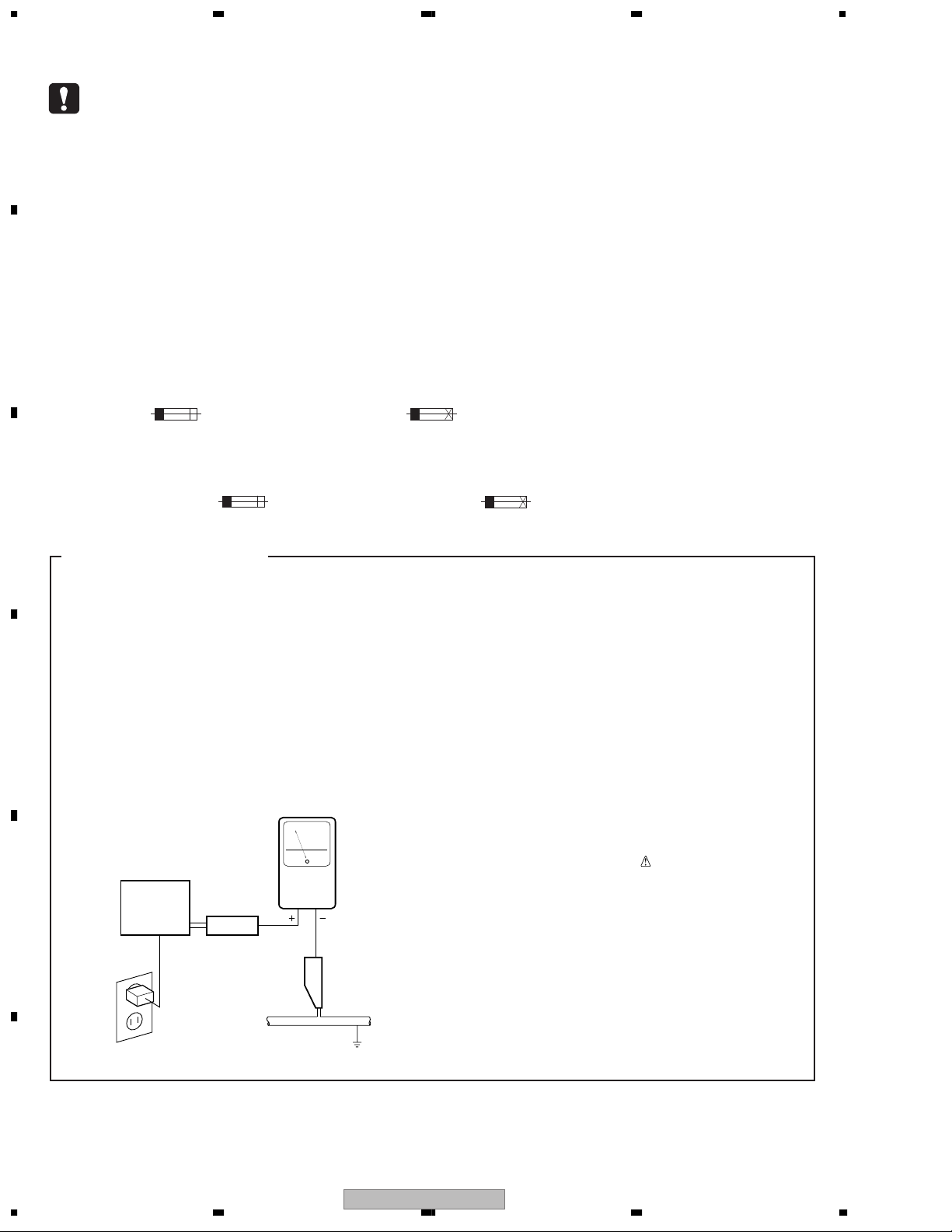
1. SAFETY PRECAUTIONS
The following check should be performed for the
continued protection of the customer and service
technician.
LEAKAGE CURRENT CHECK
Measure leakage current to a known earth ground
(water pipe, conduit, etc.) by connecting a leakage
current tester such as Simpson Model 229-2 or
D
E
equivalent between the earth ground and all exposed
metal parts of the appliance (input/output terminals,
screwheads, metal overlays, control shaft, etc.). Plug
the AC line cord of the appliance directly into a 120V
AC 60 Hz outlet and turn the AC power switch on. Any
current measured must not exceed 0.5 mA.
Reading should
not be above
0.5 mA
Earth
ground
Device
under
test
Also test with
plug reversed
(Using AC adapter
plug as required)
Test all
exposed metal
surfaces
Leakage
current
tester
AC Leakage Test
ANY MEASUREMENTS NOT WITHIN THE
LIMITS OUTLINED ABOVE ARE INDICATIVE
OF A POTENTIAL SHOCK HAZARD AND
MUST BE CORRECTED BEFORE RETURNING THE APPLIANCE TO THE CUSTOMER.
2. PRODUCT SAFETY NOTICE
Many electrical and mechanical parts in the appliance
have special safety related characteristics. These are
often not evident from visual inspection nor the
protection afforded by them necessarily can be obtained
by using replacement components rated for voltage,
wattage, etc. Replacement parts which have these
special safety characteristics are identified in this
Service Manual.
Electrical components having such features are
identified by marking with a
on the parts list in this Service Manual.
The use of a substitute replacement component which
does not have the same safety characteristics as the
PIONEER recommended replacement one, shown in the
parts list in this Service Manual, may create shock, fire,
or other hazards.
Product Safety is continuously under review and new
instructions are issued from time to time. For the latest
information, always consult the current PIONEER
Service Manual. A subscription to, or additional copies
of, PIONEER Service Manual may be obtained at a
nominal charge from PIONEER.
on the schematics and
F
2
1234
DV-563A-S
Page 3
5 678
[ Important symbols for good services ]
In this manual, the symbols shown-below indicate that adjustments, settings or cleaning should be made securely.
When you find the procedures bearing any of the symbols, be sure to fulfill them:
1. Product safety
You should conform to the regulations governing the product (safety, radio and noise, and other regulations), and
should keep the safety during servicing by following the safety instructions described in this manual.
2. Adjustments
To keep the original performances of the product, optimum adjustments or specification confirmation is indispensable.
In accordance with the procedures or instructions described in this manual, adjustments should be performed.
3. Cleaning
For optical pickups, tape-deck heads, lenses and mirrors used in projection monitors, and other parts requiring cleaning,
proper cleaning should be performed to restore their performances.
4. Shipping mode and shipping screws
To protect the product from damages or failures that may be caused during transit, the shipping mode should be set or
the shipping screws should be installed before shipping out in accordance with this manual, if necessary.
A
B
5. Lubricants, glues, and replacement parts
Appropriately applying grease or glue can maintain the product performances. But improper lubrication or applying
glue may lead to failures or troubles in the product. By following the instructions in this manual, be sure to apply the
prescribed grease or glue to proper portions by the appropriate amount.For replacement parts or tools, the prescribed
ones should be used.
• Manufactured under license from Dolby
Laboratories. “Dolby” and the double-D symbol
are trademarks of Dolby Laboratories.
• “DTS” and “DTS Digital Out” are registered
trademarks of Digital Theater Systems, Inc.
• TruSurround and the symbol are
trademarks of SRS Labs, Inc. TruSurround technology is incorporated under license from SRS
Labs, Inc.
C
D
56
DV-563A-S
E
F
7
8
3
Page 4

1234
CONTENTS
SAFETY INFORMATION ..................................................................................................................................... 2
A
B
C
D
1. SPECIFICATIONS ............................................................................................................................................ 5
2. EXPLODED VIEWS AND PARTS LIST ............................................................................................................ 6
2.1 PACKING ................................................................................................................................................... 6
2.2 EXTERIOR SECTION................................................................................................................................ 8
2.3 FRONT PANEL SECTION ....................................................................................................................... 10
2.4 LOADING MECHA ASSY ........................................................................................................................12
2.5 TRAVERSE MECHA ASSY-S .................................................................................................................. 14
3. BLOCK DIAGRAM AND SCHEMATIC DIAGRAM..........................................................................................16
3.1 BLOCK DIAGRAM ................................................................................................................................... 16
3.2 LOAB ASSY and OVERALL WIRING DIAGRAM..................................................................................... 18
3.3 DVDM ASSY 1/3 [FRONT END BLOCK]................................................................................................. 20
3.4 DVDM ASSY 2/3 [BACK END BLOCK].................................................................................................... 22
3.5 DVDM ASSY 3/3 [SACD and POWER SUPPLY BLOCK] ........................................................................ 24
3.6 JCKB ASSY 1/2 [AUDIO BLOCK]............................................................................................................ 26
3.7 JCKB ASSY 2/2 [VIDEO BLOCK]............................................................................................................ 28
3.8 FLKY and PWSB ASSYS ........................................................................................................................ 30
3.9 POWER SUPPLY UNIT............................................................................................................................ 32
3.10 WAVEFORMS ........................................................................................................................................ 33
4. PCB CONNECTION DIAGRAM ..................................................................................................................... 35
4.1 LOAB ASSY............................................................................................................................................. 35
4.2 DVDM ASSY............................................................................................................................................ 36
4.3 JCKB ASSY .............................................................................................................................................38
4.4 FLKY and PWSB ASSYS ........................................................................................................................ 40
4.5 POWER SUPPLY UNIT............................................................................................................................ 42
5. PCB PARTS LIST ........................................................................................................................................... 43
6. ADJUSTMENT ............................................................................................................................................... 46
6.1 ADJUSTMENT ITEMS AND LOCATION ................................................................................................. 46
6.2 JIGS AND MEASURING INSTRUMENTS............................................................................................... 46
6.3 NECESSARY ADJUSTMENT POINTS ...................................................................................................47
6.4 TEST MODE ............................................................................................................................................ 48
6.5 MECHANISM ADJUSTMENT.................................................................................................................. 49
7. GENERAL INFORMATION............................................................................................................................. 51
7.1 DIAGNOSIS ............................................................................................................................................. 51
7.1.1 TEST MODE ......................................................................................................................................... 51
7.1.2 DISPLAY SPECIFICATION OF THE TEST MODE ...............................................................................53
7.1.3 FUNCTIONAL SPECIFICATION OF THE SHORTCUT KEY................................................................ 54
7.1.4 SPECIFICATION OF MODEL INFORMATION DISPLAY...................................................................... 55
7.1.5 FUNCTIONAL SPECIFICATION OF THE SERVICE MODE.................................................................56
7.1.6 MECHANICAL ERROR HISTORY ........................................................................................................ 57
7.1.7 ID NUMBER AND ID DATA SETTING................................................................................................... 60
7.1.8 TROUBLE SHOOTING ......................................................................................................................... 63
7.1.9 SEQUENCE AFTER POWER ON ........................................................................................................ 65
7.1.10 DISASSEMBLY ...................................................................................................................................66
7.2 IC ............................................................................................................................................................. 74
7.3 DISC / CONTENT FORMAT PLAYBACK COMPATIBILITY .....................................................................90
7.4 CLEANING............................................................................................................................................... 92
8. PANEL FACILITIES ........................................................................................................................................ 93
E
F
4
1234
DV-563A-S
Page 5

5 678
1. SPECIFICATIONS
General
System . . . . . . . . . . . . . . . . . . . . . . . . . DVD player
Power requirements
. . . . . . . . . . . . . . . . . . . AC 120 V, 60 Hz
Power consumption
. . . . . . . . . . . . . . . . . . . . . . . . . . . . . 14 W
Power consumption (standby)
. . . . . . . . . . . . . . . . . . . . . . . . . . . 0.12 W
Weight . . . . . . . . . . . . . . . . . . . . . 2.4 kg / 5 lb 3 oz
Dimensions . . . . 420 (W) x 55 (H) x 283 (D) mm
(16.5 (W) x 2.2 (H) x 11.1 (D) in.)
Operating temperature . . . . . . . . . . +5°C to +35°C
(+41°F to +95°F)
Operating humidity . . . . . . . . . . . . . . . . 5% to 85%
(no condensation)
Component video output
Y (luminance) - Output level . . . . . . . . 1 Vp-p (75 Ω)
P
(color) - Output level . . . . . . . . . 0.7 Vp-p (75 Ω)
B
(color) - Output level . . . . . . . . . 0.7 Vp-p (75 Ω)
P
R
Jack . . . . . . . . . . . . . . . . . . . . . . . . . . . . . RCA jacks
Number of channels . . . . . . . . . . . . . . . . . . . . . . . 2
Jacks . . . . . . . . . . . . . . . . . . . . . . . . . . . . RCA jack
Audio output (multi-channel / L, R, C,
SW, LS, RS)
Output level . . . . . . . . . . . . . . . During audio output
200 mVrms (1 kHz, –20 dB)
Number of channels . . . . . . . . . . . . . . . . . . . . . . . 6
Jacks . . . . . . . . . . . . . . . . . . . . . . . . . . . . RCA jack
Digital audio characteristics
Frequency response
. . . . . . . . . . . . . . . 4 Hz to 44 kHz (DVD fs: 96 kHz)
. . . . . . . . . 4 Hz to 88 kHz (DVD-Audio fs: 192 kHz)
S/N ratio . . . . . . . . . . . . . . . . . . . . . . . . . . . . 118 dB
Dynamic range
. . . . . . . . . . . . . . . . . . . . . . . 108 dB
Total harmonic distortion . . . . . . . . . . . . . 0.0014 %
Wow and flutter. . . . . . . . . . Limit of measurement
(±0.001% W. PEAK) or lower
Digital output
Optical digital output . . . . . . . . . Optical digital jack
Coaxial digital output . . . . . . . . . . . . . . . . RCA jack
Other terminals
Control in . . . . . . . . . . . . . . . . . . . . Minijack (3.5 ø)
Control out . . . . . . . . . . . . . . . . . . . Minijack (3.5 ø)
A
B
C
S-video output
Y (luminance) - Output level . . . . . . . . 1 Vp-p (75 Ω)
C (color) - Output level . . . . . . . . 286 mVp-p (75 Ω)
Jack . . . . . . . . . . . . . . . . . . . . . . . . . . . S-video jack
Video output
Output level . . . . . . . . . . . . . . . . . . . . 1 Vp-p (75 Ω)
Jack . . . . . . . . . . . . . . . . . . . . . . . . . . . . . RCA jack
Audio output (1 stereo pair)
Output level . . . . . . . . . . . . . . . During audio output
200 mVrms (1 kHz, –20 dB)
Accessories
Audio/video cable (DV-563A-S only). . . . . . . . . . 1
Power cable . . . . . . . . . . . . . . . . . . . . . . . . . . . . . 1
Remote control (
AA/R6P dry cell batteries (
DV-563A-S only). . . . . . . . . . . . 1
DV-563A-S only) . . . . . 2
Operating Instructions
. . . . . . . . . . . . . . . . . . . . . . . . . . . . . . . . 1
Warranty card (
DV-563A-S only)
. . . . . . . . . . . . . 1
• The specifications and design of this
product are subject to change without
notice, due to improvement.
D
E
56
DV-563A-S
F
7
8
5
Page 6
1234
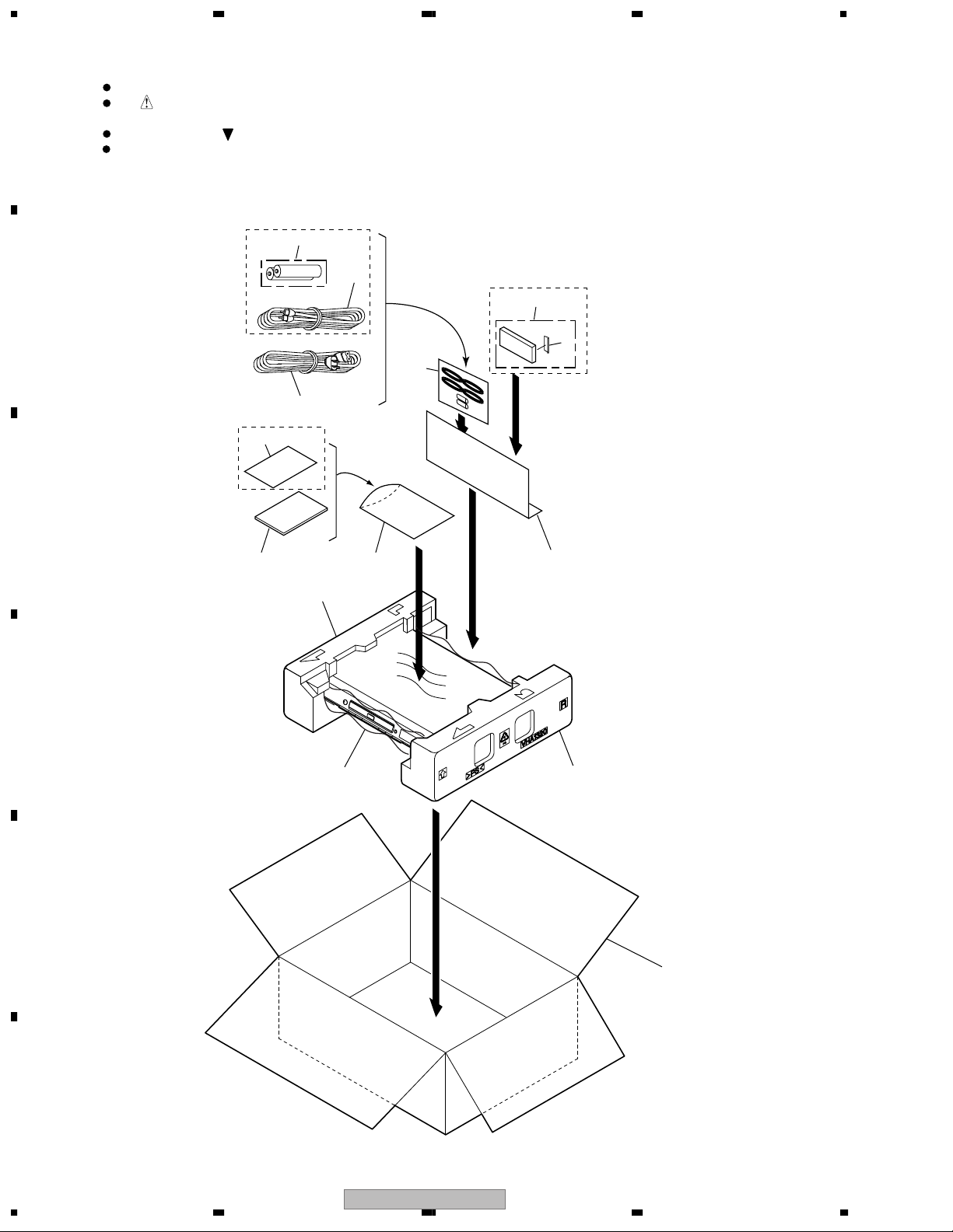
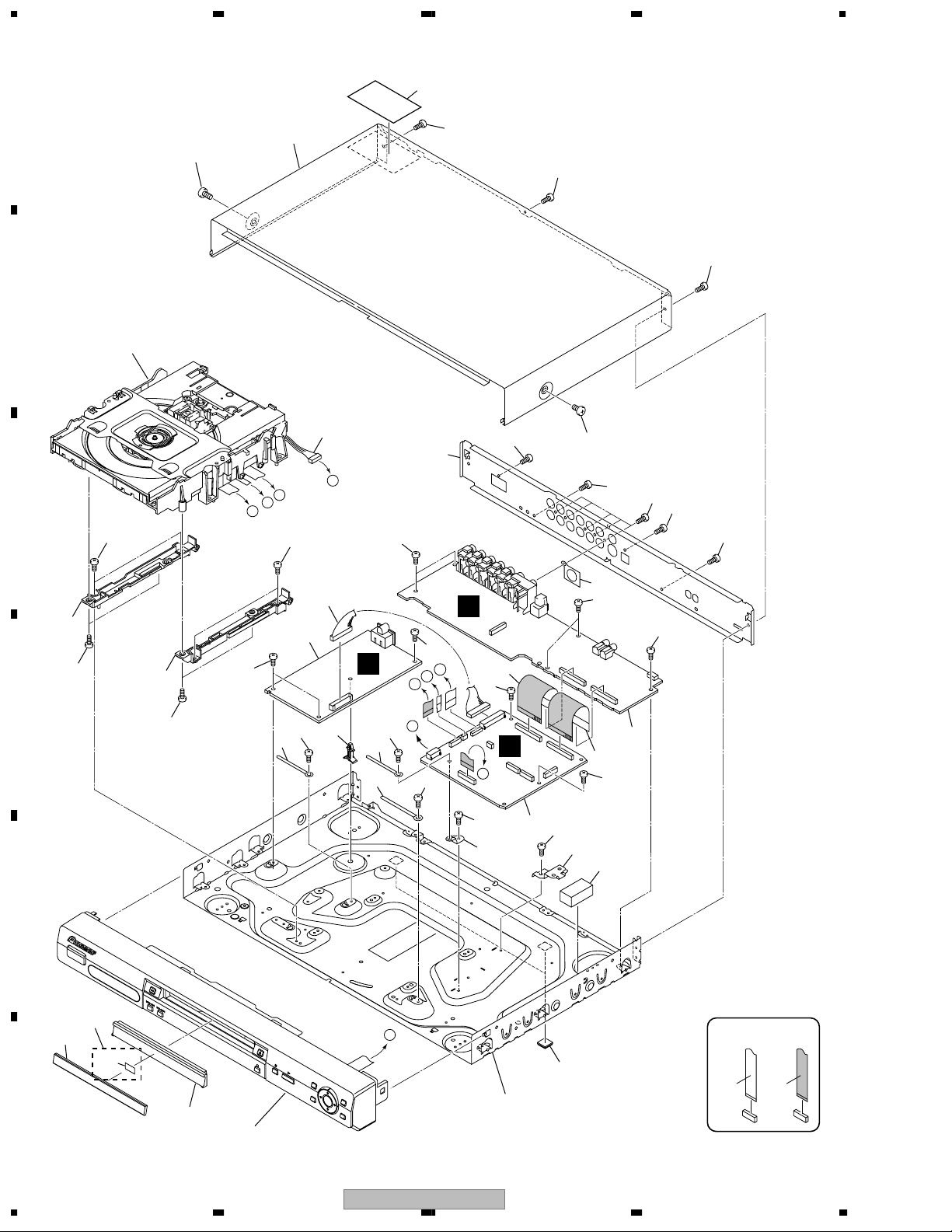
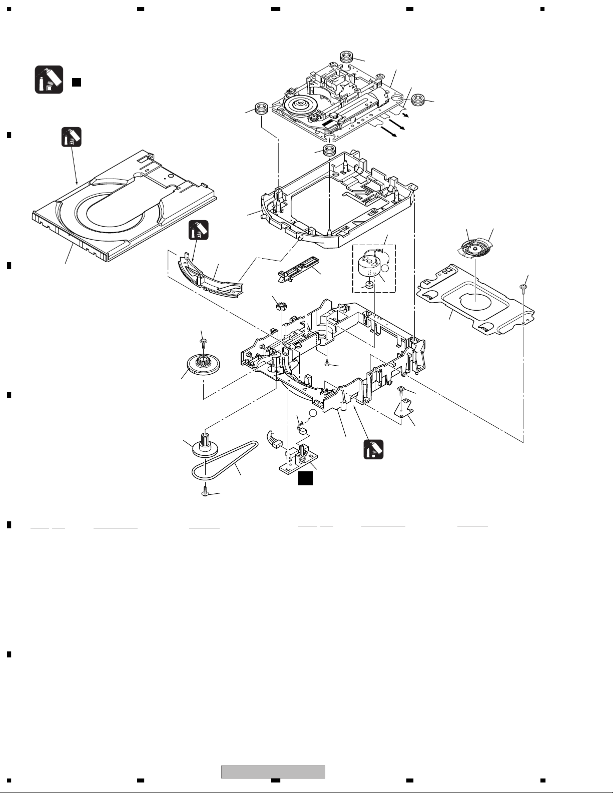
2. EXPLODED VIEWS AND PARTS LIST
NOTES:
A
2.1 PACKING
B
C
Parts marked by "NSP" are generally unavailable because they are not in our Master Spare Parts List.
The mark found on some component parts indicates the importance of the safety factor of the part.
Therefore, when replacing, be sure to use parts of identical designation.
Screws adjacent to mark on product are used for disassembly.
For the applying amount of lubricants or glue, follow the instructions in this manual.
(In the case of no amount instructions, apply as you think it appropriate.)
DV-563A-S
Only
DV-563A-S
Only
5
2
3
8
1
7
DV-563A-S
Only
4
6
9
D
E
8
13
11
10
12
F
6
1234
DV-563A-S
Page 7
>
5 678
PACKING parts List
Mark
Mark
No. Description Part No.
1Power Cable ADG7021
2Audio / Video Cable See Contrast table (2)
3 Remote Control Unit See Contrast table (2)
4 Battery Cover See Contrast table (2)
NSP 5 Dry Cell Battery (R6P, AA) See Contrast table (2)
6 Operating Instructions See Contrast table (2)
(English)
NSP 7 Warranty Card See Contrast table (2)
8Polyethylene Bag VHL1051
9Pad L VHA1319
10 Pad R VHA1320
No. Description Part No.
11 Paper Board VHC1100
12 Packing Case See Contrast table (2)
13 Sheet (750 x 600 x 0.5) Z23-007
(2) CONTRAST TABLE
DV-563A-S/KUXU/CA and DV-50A/KUXU/CA are constructed the same except for the following :
A
B
Mark No. Symbol and Description
2Audio / Video Cable VDE1077 Not used
3 Remote Control Unit VXX2865 Not used
4 Battery Cover VNK4997 Not used
NSP 5 Dry Cell Battery (R6P, AA) VEM1030 Not used
6 Operating Instructions (English) VRB1311 VRB1313
NSP 7 Warranty Card ARY7045 Not used
12 Packing Case VHG2336 VHG2380
DV-563A-S/
KUXU/CA
DV-50A/KUXU/
CA
C
D
56
DV-563A-S
E
F
7
8
7
Page 8
1234
2.2 EXTERIOR SECTION
A
27
24
21
26
26
26
B
C
19
28
D
Refer to
"2.4 LOADING MECHA. ASSY".
5
B
26
20
28
25
6
14
26
25
E
25
8
4
F
12
25
10
10
25
D
C
B
E
25
D
C
10
C
28
7
25
B
A
27
18
25
7
25
26
26
28
26
25
2
E
F
DV-563A-S
Only
23
8
30
Refer to
"2.3 FRONT PANEL SECTION".
22
25
16
A
15
1
25
17
13
11
NON-CONTACT
SIDE
CONTACT SIDE
DV-563A-S
1234
Page 9
>
5 678
EXTERIOR SECTION parts List
Mark
No. Description Part No.
1DVDM Assy VWS1563
2 JCKB Assy VWV1942
3• • • • •
4POWER SUPPLY Unit VWR1365
NSP 5 Loading Mecha. Assy VWT1207
Mark
No. Description Part No.
16 PCB Base VNE2278
17 PCB Base VNE2310
NSP 18 S Earth Plate VNF1128
19 Adapter 3L VNL1960
20 Adapter 3R VNL1961
A
6 Connector Assy PG05KK-E37
7 Flexible Cable (33P) VDA1956
8 Connector Assy (13P) VKP2310
9• • • • •
10 Cord Clamper RNH-184
11 Rubber Foot VEB1349
12 PCB Support VEC2184
13 Cushion VEC2342
14 Rear Panel See Contrast table (2)
NSP 15 Base Chassis VNA2614
21 Bonnet Case S VXX2874
22 Tray Panel VNK5280
23 Acryl Door See Contrast table (2)
24 KUC Label VRW1959
25 Screw BBZ30P060FMC
26 Screw BBZ30P080FZK
27 Screw BCZ40P060FNI
28 Screw PPZ30P080FMC
29 • • • • •
30 Hologram Sheet See Contrast table (2)
(2) CONTRAST TABLE
DV-563A-S/KUXU/CA and DV-50A/KUXU/CA are constructed the same except for the following :
Mark No. Symbol and Description
14 Rear Panel VNA2578 VNA2574
23 Acryl Door VEC2338 VEC2361
30 Hologram Sheet VEC2359 Not used
DV-563A-S/
KUXU/CA
DV-50A/KUXU/
CA
B
C
D
E
F
56
DV-563A-S
7
8
9
Page 10
1234
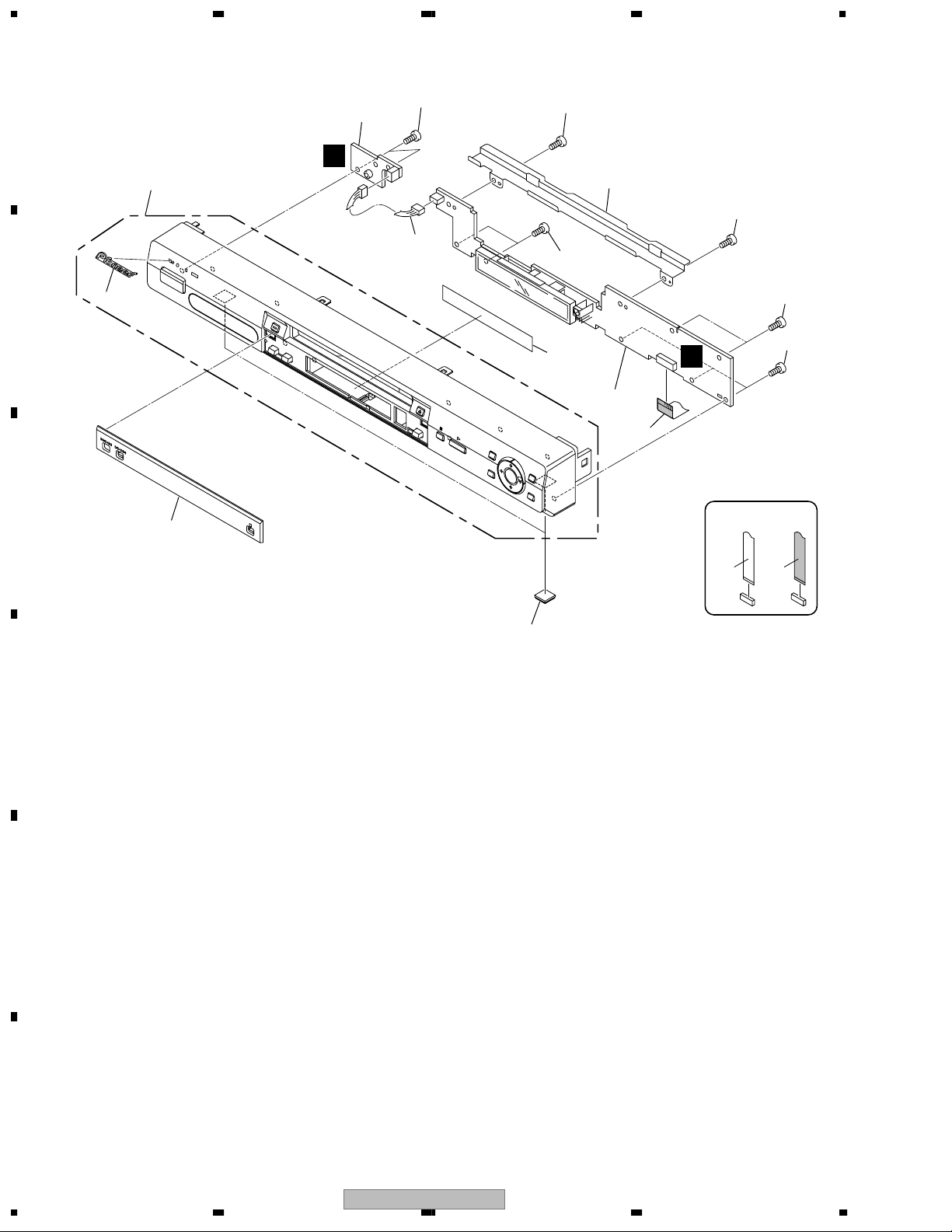
2.3 FRONT PANEL SECTION
A
2
12
12
E
10
3
12
B
C
11
7
6
9
12
12
12
D
1
4
NON-CONTACT
5
D
E
SIDE
CONTACT SIDE
F
10
1234
DV-563A-S
Page 11
5 678
FRONT PANEL SECTION parts List
Mark
Mark
No. Description Part No.
1 FLKY Assy See Contrast table (2)
NSP 2 PWSB Assy VWG2429
3 Connector Assy PF03PP-B07
4 Flexible Cable (21P) VDA1957
5 Rubber Foot VEB1349
6 FL Lens VEC2336
7 FL Filter VEC2339
8• • • • •
9 FP Angle VNE2300
10 Front Panel Assy See Contrast table (2)
No. Description Part No.
11 Pioneer Name Plate See Contrast table (2)
12 Screw PPZ30P080FMC
(2) CONTRAST TABLE
DV-563A-S/KUXU/CA and DV-50A/KUXU/CA are constructed the same except for the following :
A
B
Mark No. Symbol and Description
1 FLKY Assy VWG2427 VWG2430
10 Front Panel Assy VXA2576 VXA2575
11 Pioneer Name Plate VAM1129 Not used
11 Pioneer Name Plate B Not used PAN1376
DV-563A-S/
KUXU/CA
DV-50A/KUXU/
CA
C
D
56
DV-563A-S
E
F
7
8
11
Page 12
1234
2.4 LOADING MECHA ASSY
Note :
A
Refer to
" Application of Lubricant".
8
Daifree
GEM1036
B
12
Lubricating Oil
GYA1001
23
C
13
16
22
8
17
8
4
Refer to
2
"2.5 TRAVERSE MECHA. ASSY-S".
6
8
To DVDM CN101 (Pickup Assy-S)
To DVDM CN104 (Stepping Motor)
To DVDM CN102 (Spindle Motor)
3
A
5
18
19
20
22
D
LOADING MECHA ASSY parts List
Mark
No. Description Part No.
NSP 1 LOAB Assy VWG2426
2Traverse Mecha. Assy-S VXX2871
3 Loading Motor Assy VXX2872
4 Motor Pulley PNW1634
5 Motor VXM1105
E
6 Flexible Cable (24P) VDA1945
7 Connector Assy 2P VKP2253
8 Floating Rubber VEB1351
9 Belt VEB1330
10 Stabilizer VNE2253
15
14
22
21
22
7
A
10
11
9
1
A
Mark No. Description Part No.
17 SW Lever VNL1925
18 Clamper Plate VNE2251
19 Bridge VNE2252
20 Clamper VNL1924
21 Screw JGZ17P028FMC
22 Screw Z39-019
23 Tray VNL1920
Lubricating Oil
GYA1001
11 Loading Base VNL1917
12 Float Base DVD VNL1918
13 Drive Cam VNL1919
14 Gear Pulley VNL1921
F
15 Loading Gear VNL1922
16 Drive Gear VNL1923
12
1234
DV-563A-S
Page 13
5 678
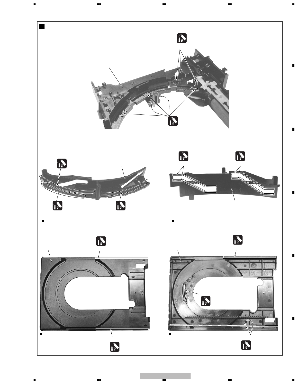
Application of Lubricant
No. 11
Loading Base
Lubricating Oil
GYA1001
Around the shaft
Lubricating Oil
GYA1001
A
B
Lubricating Oil
GYA1001
Lubricating Oil
GYA1001
No. 13
Drive Cam
Lubricating Oil
GYA1001
Inner side of a ditch
Front View Rear View
No. 23
Tray
Daifree
GEM1036
Concave of unevenness
No. 23
Tray
Lubricating Oil
GYA1001
Inner side of a ditch
Daifree
GEM1036
Lubricating Oil
GYA1001
Inner side of a ditch
No. 13
Drive Cam
Daifree
GEM1036
Concave of unevenness
C
D
E
Top View
Bottom View
Concave of unevenness
Daifree
GEM1036
DV-563A-S
56
Side of the rib
Daifree
GEM1036
7
8
F
13
Page 14
1234
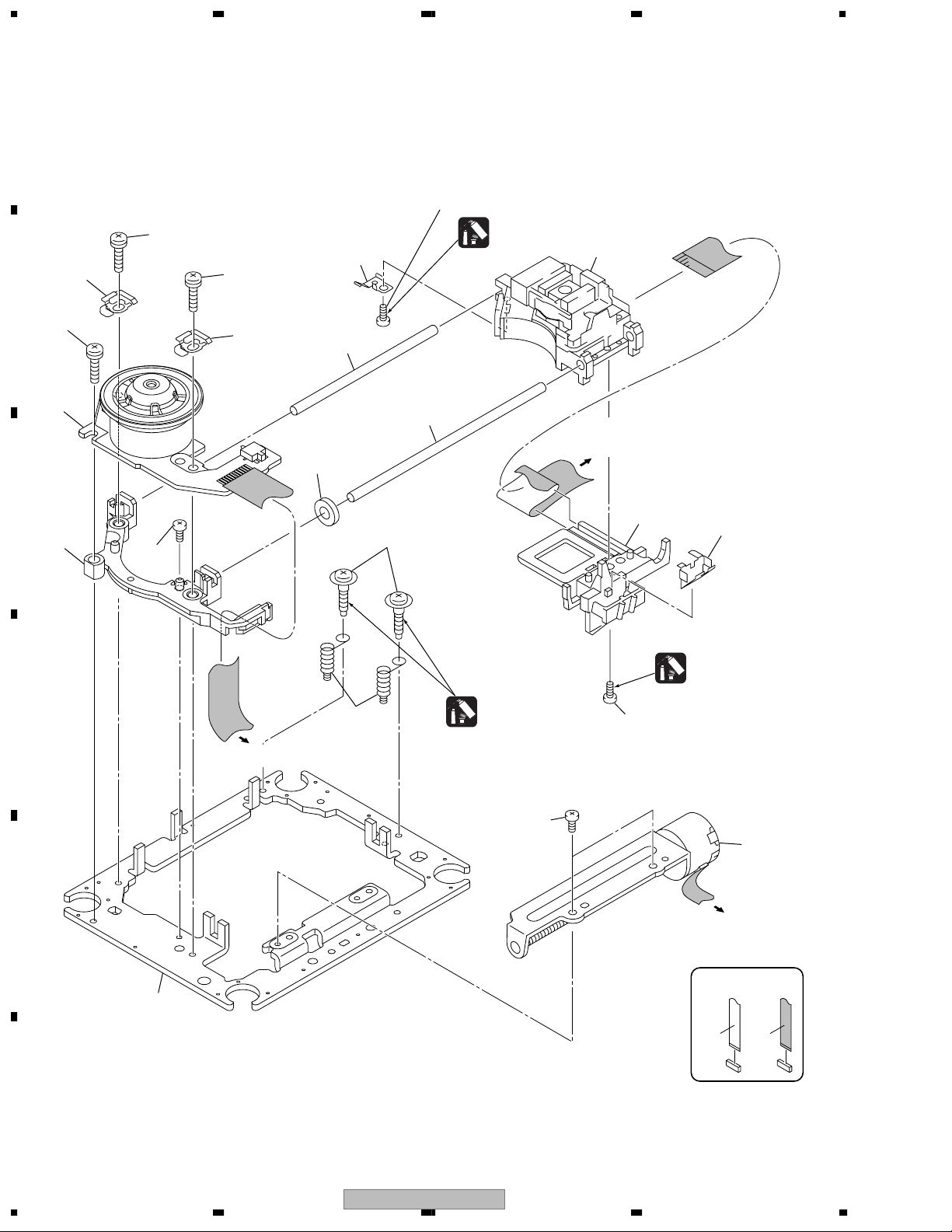
2.5 TRAVERSE MECHA ASSY-S
A
15 (Torque : 0.15 ± 0.01 N•m)
17
8
10
B
17
1
17
10
7
6
Silicone Adhesive
GEM1037
3
To
DVDM CN101
(Pickup Assy)
12
C
13
16
4 (Adjustment screw)
14
9
Silicone Adhesive
GEM1037
D
To DVDM CN102
(Spindle Motor)
5
(Adjustment
spring)
Screw Tight
GYL1001
15 (Torque : 0.15 ± 0.01 N•m)
16
2
E
To
DVDM CN104
(Stepping Motor)
11
NON-CONTACT
F
SIDE
CONTACT SIDE
14
1234
DV-563A-S
Page 15

5 678
TRAVERSE MECHA ASSY-S parts List
Mark
No. Description Part No.
1 Spindle Motor VXM1099
2 Stepping Motor VXM1101
3 Pickup Assy-S OXX8005
4Skew Screw VBA1080
5Skew Spring VBH1335
6 Guide Bar VLL1514
7 Sub Guide Bar VLL1515
8 Leaf Spring VNC1023
9 Joint Spring VNC1019
10 Support Spring VNC1020
NSP 11 Mecha.Chassis VNE2248
12 Damper Sheet VEB1335
13 Spacer VNL1913
14 Joint 03 VNL1949
15 Tapping Screw OBA8021
16 Screw BBZ20P050FZK
17 Screw PMA26P100FMC
A
B
C
D
E
56
DV-563A-S
F
7
8
15
Page 16
1234
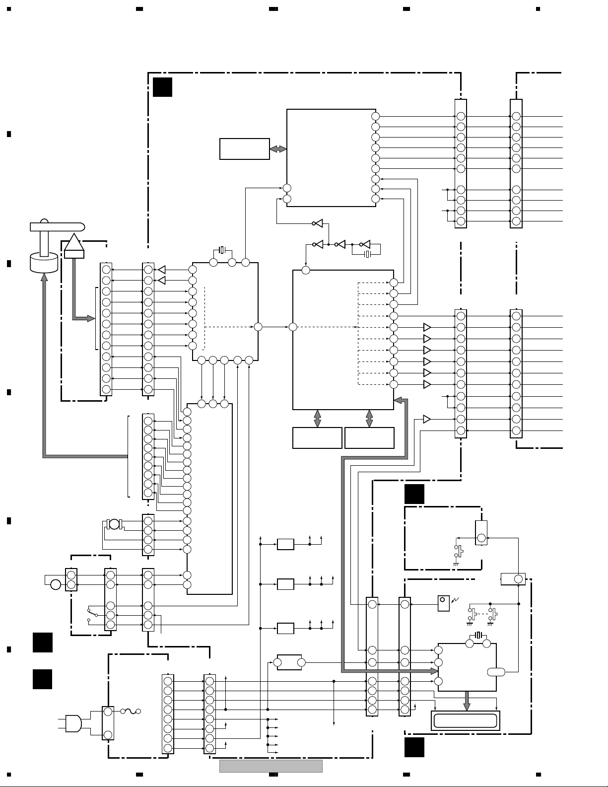
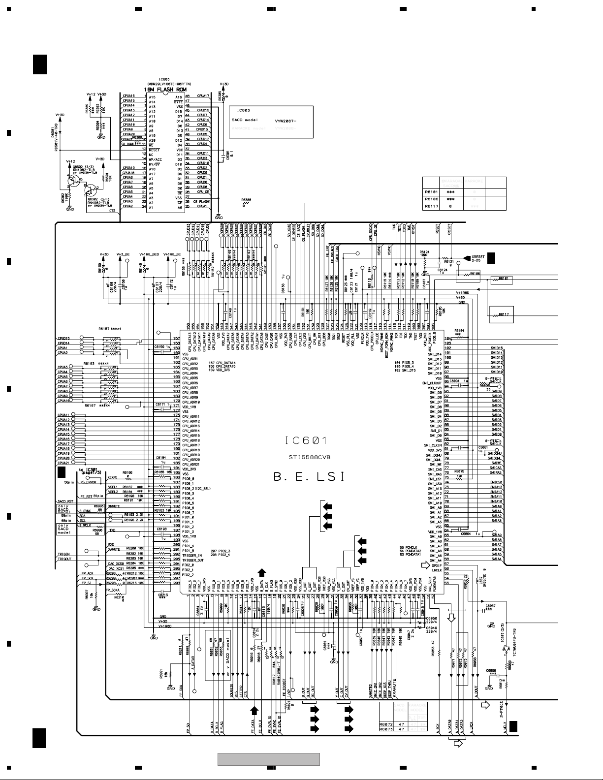
3. BLOCK DIAGRAM AND SCHEMATIC DIAGRAM
3.1 BLOCK DIAGRAM
A
DVDM ASSY
B
(3/3)(2/3)
PCMDATA2
PCMDATA1
PCMDATA0
CV_OUT
IC602
20
21
12
10
14
11
CN105
(21P)
DSD L/PCMDATA0
108
DSD R
109
DSD C/PCMDATA1
110
DSD LFE
111
DSD LS/PCMDATA2
113
DSD RS
114
40
39
41
X6401
27MHz
54
53
52
A DOUT
SPDIF
57
RC_OUT
R_OUT
27
G_OUT
26
B_OUT
25
CV_OUT
34
C_OUT
33
Y_OUT
32
IR
SEL IR
RESET
8 8
VFDP
FL DC+
FL DC-
V+3E
CN104
(21P)
V+3A
V+12
A DATA2
A DATA1
A DATA0
Q531
G_OUT
B_OUT
C_OUT
Y_OUT
20
21
12
10
14
11
Q541
Q551
Q511
Q501
Q521
V+6B
Q6972
PWSB ASSY
E
POWER
17
-28V
60
V+3E
FLKY ASSY
D
IR101
Remote Sensor Unit
6
DSD_PCM_0
DSD_PCM_1
DSD_PCM_2
DSD_PCM_3
DSD_PCM_4
DSD_PCM_5
PCM_LSRS_IN
PCM_LERI_IN
PCM_CELF_IN
IC606
(1/3)
TC7WU04FU
1
(1/3)
265 3
IC604
TC7WU04FU
IC601
V+5
V+5D
V+_3A
V+3_033
V+3DV+3_FED
V+3_FEA
V+3_333
V-28
K4S281632D-TC75
128M SDRAM
IC702
K4S641632F-TC75
64M SDRAM
SACD_RF
OUT
IC301
OUT_DATA
PD(0)
55
LOAD DRV
LOIN+
V+3E
V+6
V+12
SACD_27MHz
SACD_RF
99
RF
SACD
64
PE(1)38PC(2)
70
OPEN
XCLOSE
V+6B
DV-563A-S
FE DATA
MM1565AF
5V REG.
PQ033EZ01ZP
3V REG.
PQ1L333M2SP
3V REG.
B
X301
20MHz
CN1013
SPINDLE
MOTOR
OEIC
C
PICKUP
ASSY-S
(24P)
7
9
17
19
16
15
22
21
4
3
2
1
D
STEPPING
MOTOR
CN602
2 1
+–
1 2
E
M
LOADING
MOTOR
ASSY
S101
LOAB ASSY
A
M
3
4
5 5
POWER
F
SUPPLY
UNIT
F
AC IN
NEUTRAL
LIVE
CN1
1
2
LD(650)
LD(780)
A
C
B1
B2
B3
B4
TRKG DRV
TRKG RTN
FOCS DRV
FOCS RTN
H3–
H3+
H2–
H2+
H1–
H1+
ST2–
ST2+
ST1+
ST1–
LOAD–
LOAD+
SW2
V+3D
SW1
CN101
(24P)
18
16
10
21
22
23
24
CN102
(12P)
A1
A2
A3
CN104
CN103CN601
8
6
9
3
4
9
8
7
6
5
4
3
2
1
4
3
2
1
1
2
3
4
Q201,
Q202
Q211,
Q212
XCLOSE
OPEN
V+3_FED
CN101
(13P)
13
12
11
8
7
5
4
2
89
90
21
20
6
8
14
12
PC(0)
FG
TO–
30
TO+
31
FO+
34
FO–
35
16
17
18
19
20
21
14
13
12
6
5
9
10
36
37
-28V
FL DC+
FL DC-
EV+3.3V
SW+1.8V
EV+6V(A)
EV+6V(B)
SW+12V
87 86
LD1
FREINFRE
LD2
E
STM6316ATXXA
F
Front End IC
A
B
C
D
44
36
FG
SPDL PDM
26 40
24
HW–
HW+
HV–
HV+
HU–
HU+
U
V
W
SL2–
SL2+
SL1+
SL1–
IC101
M63018FP
FTS Driver
LO+
LO–
CN401
(13P)
13
12
11
8
7
5
4
2
PC(6)
SPIN
16
SAA7893HL/C2
AGCINP
35
21
SYS_CLK
PIXCLK
16
16M Flash ROM
IC401
IC402
IC403
IC400
PST328
Reset
3 1
V+1R8
V+1R8_BED
V+1R8_D
V+1R8_FEA
V+1R8_FED
IC701
SACD IC
771
120
B_DATA
STI5588CVB
Back End IC
IC603
VYW2087
DSD_L/PCMDATA0
22
24
DSD_C/PCMDATA1
30
DSD_LFE
32
DSD_LS/PCMDATA2
26
28
8
9
4
5
CN601
(33P)
CN602
(33P)
29
13
17
15
23
21
19
25
26
1
2
CN103
(3P)
KEY0 - KEY2
X101
5MHz
3 4
SEL IR
X1 X2
RESET IN
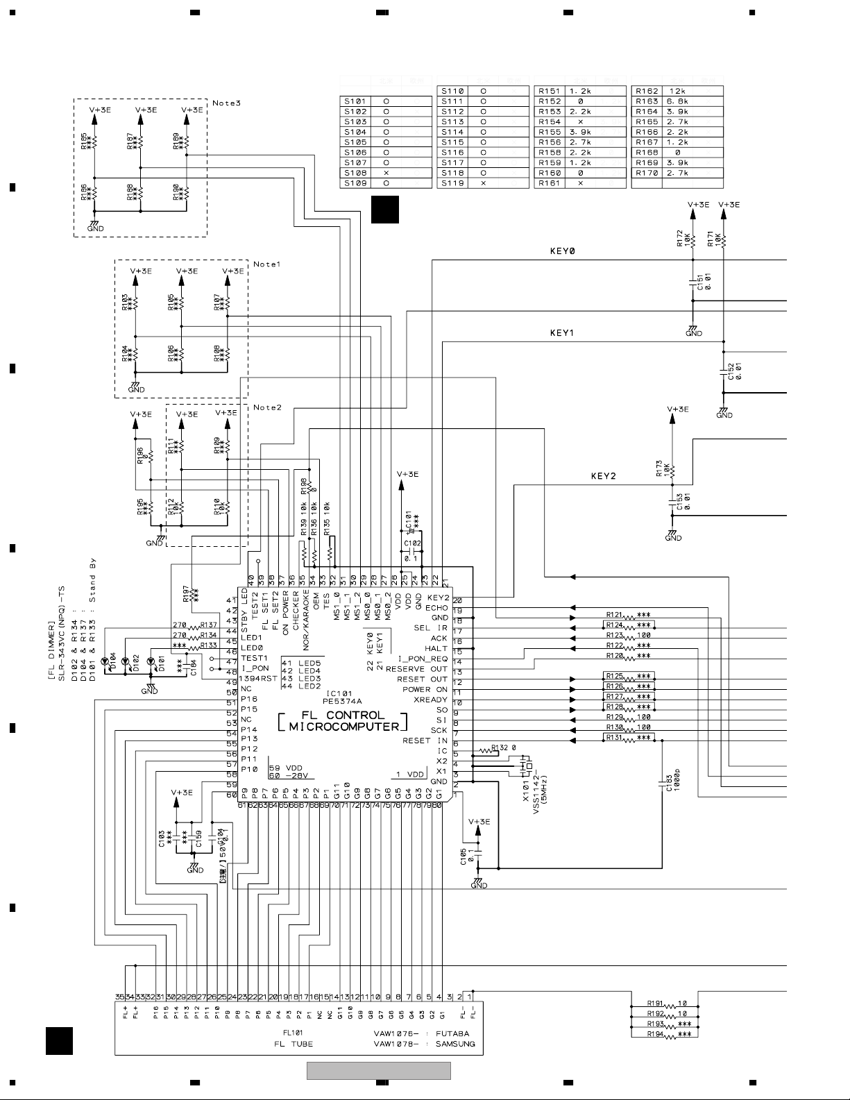
IC101
PE5374A
FL Control
Microcomputer
FL101
FL Tube
DSD_R
DSD_RS
V+3A
V+3A
V+12
V+12
A_DOUT
R_CR
G_Y
B_CB
V
S_C
S_Y
V+6
V+6
IR
SEL_IR
1
CN102
(3P)
20-22
KEY0
12
10
4
2
8
6
26
25
30
29
CN101
(33P)
CN102
(33P)
5
21
17
19
11
13
15
9
8
33
32
1
KEY0
1234
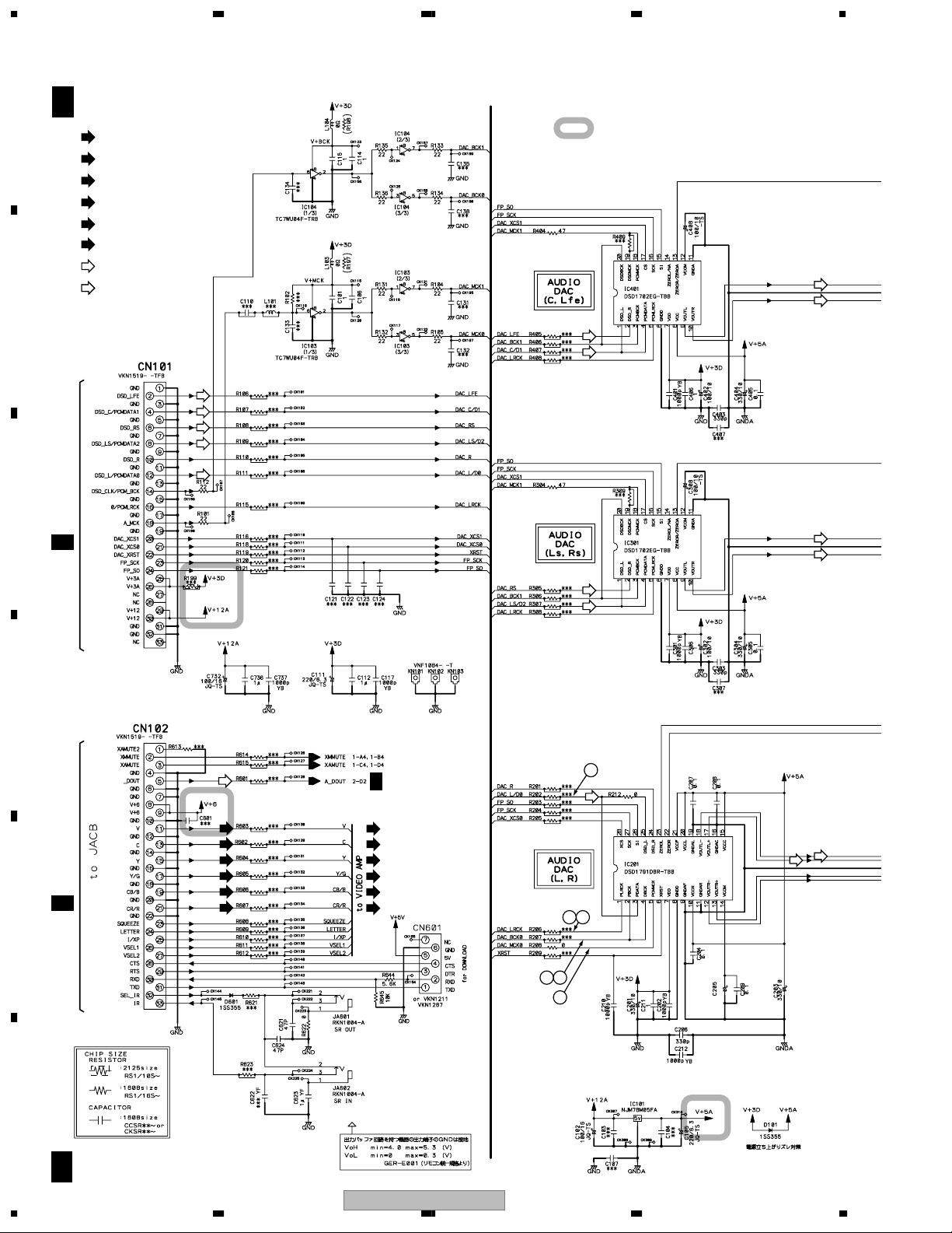
Page 17
DAC L/D0
DAC R
DAC C/D1
DAC LFE
DAC LS/D2
DAC RS
V+3D
V+12A
A_DOUT
CR/R
Y/G
CB/B
V
C
Y
V+6
5 678
A
IC201
DSD1791DBR
Audio DAC (L, R)
VOUTL+
PDATA
3
DSD_L
25
24
Audio DAC (Ls, Rs)
4
1
2
4
1
2
VOUTL–
DSD_R
VOUTR+
VOUTR–
IC301
DSD1702EG
PCMDATA
DSD_L
DSD_R
Audio DAC (C, Lfe)
PCMDATA
DSD_L
DSD_R
VOUTL
VOUTR
IC401
DSD1702EG
VOUTL
VOUTR
17
18
13
12
9
10
9
10
V+12A
IC204
BA4560F
Audio LPF & Amp.
5
7
2/2
6
3
1
1/2
2
IC302
BA4560F
Audio LPF & Amp.
3
1
1/2
2
6
7
2/2
5
IC402
BA4560F
Audio LPF & Amp.
3
1
1/2
2
6
7
2/2
5
IC101
NJM78M05FA
5V REG.
V+5A
Q101
REG.
VREF
16
11
14
2
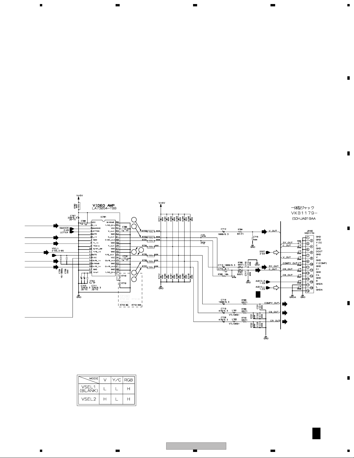
6
8
LA73054
Video Amp.
Cr_R_in
Y/G_in
Cb_B_in
V_in
C_in
Y_in
IC701
Cr_R_out
Y/G_out
Cb_B_out
V_out
C_out
Y_out
JCKB ASSY
C
JA101
L
FRONT
R
L
SURROUND
R
CENTER
SUB WOOFER
JA801
DIGITAL
AUDIO OUT
OPTICAL
JA102
Q801
21
25
23
33
31
28
(19P)
6
18
16
12
10
14
8
43C
Y
DIGITAL
AUDIO OUT
COAXIAL
L
AUDIO OUT
R
R (RED)
P
Y (GREEN)
PB (BLUE)
VIDEO OUT
S VIDEO OUT
COMPONENT
B
VIDEO OUT
C
IR
SEL IR
JA602
IN
OUT
JA601
CONTROL
V+6
IC771
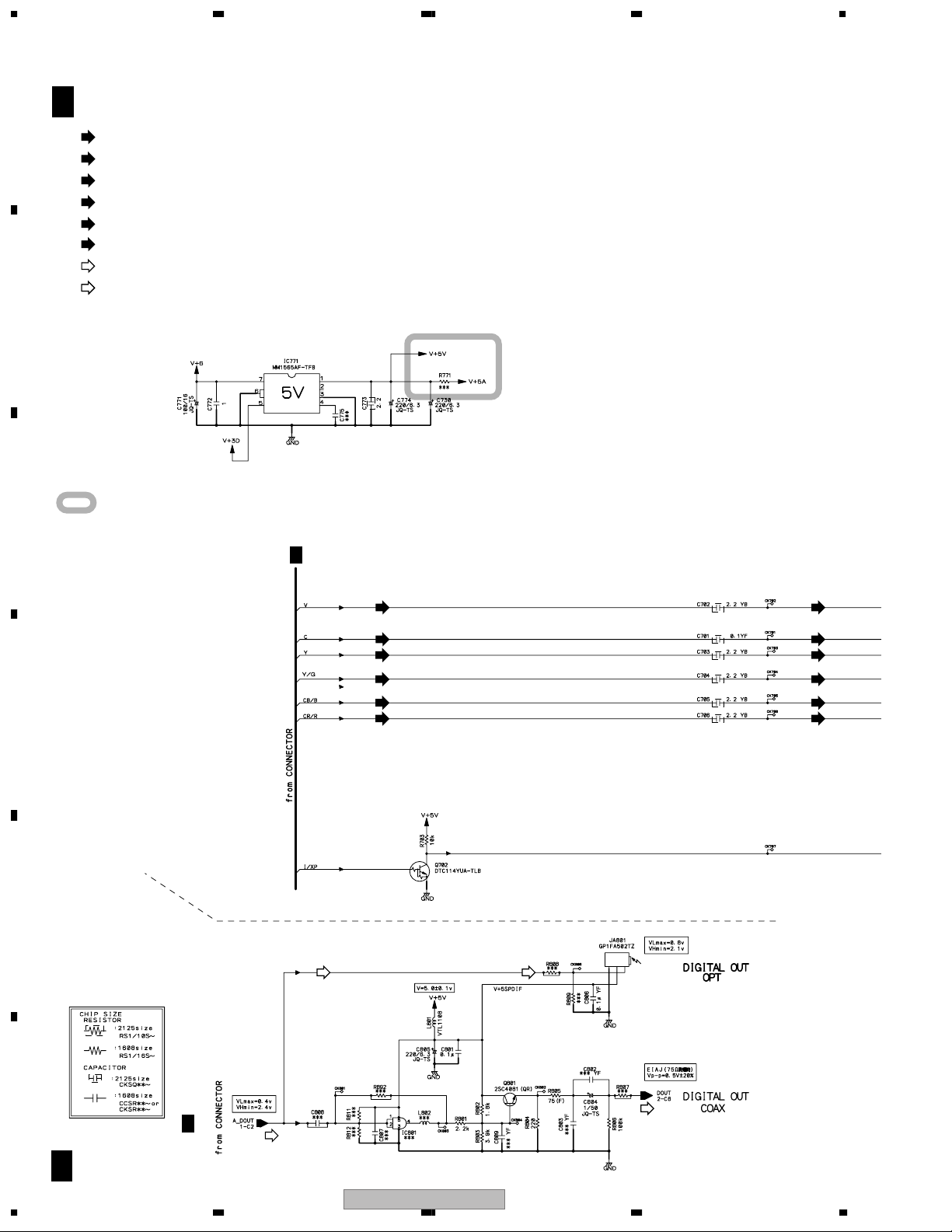
MM1565AF
5V REG.
V+5V
D
E
56
DV-563A-S
F
7
8
17
Page 18
1234
3.2 LOAB ASSY and OVERALL WIRING DIAGRAM
A
B
C
D
Note : When ordering service parts, be sure
to refer to "EXPLODED VIEWS and
PARTS LIST" or "PCB PARTS LIST".
JCKB ASSY
C
(VWV1942)
E
F
18
1234
DV-563A-S
Page 19
5 678
(F)
: RF SIGNAL ROUTE
RF
: FOCUS SERVO LOOP LINE
(T)
: TRACKING SERVO LOOP LINE
(S)
: STEPPING SERVO LOOP LINE
A
PWSB ASSY
D
FLKY ASSY
(DV-563A-S: VWG2427)
(DV-50A: VWG2430)
E
(VWG2429)
B
PICKUP ASSY-S
(OXX8005)
DVDM ASSY
B
(VWS1563)
RF
RF
RF
RF
RF
RF
F
T
T
F
STEPPING MOTOR
S
: VXM1101
S
S
S
LOAB ASSY
A
(VWG2426)
SPINDLE
MOTOR
: VXM1099
LOADING
MOTOR ASSY
: VXX2872
C
D
F
POWER SUPPLY UNIT
(VWR1365)
DV-563A-S
56
E
F
A
7
8
19
Page 20
1234
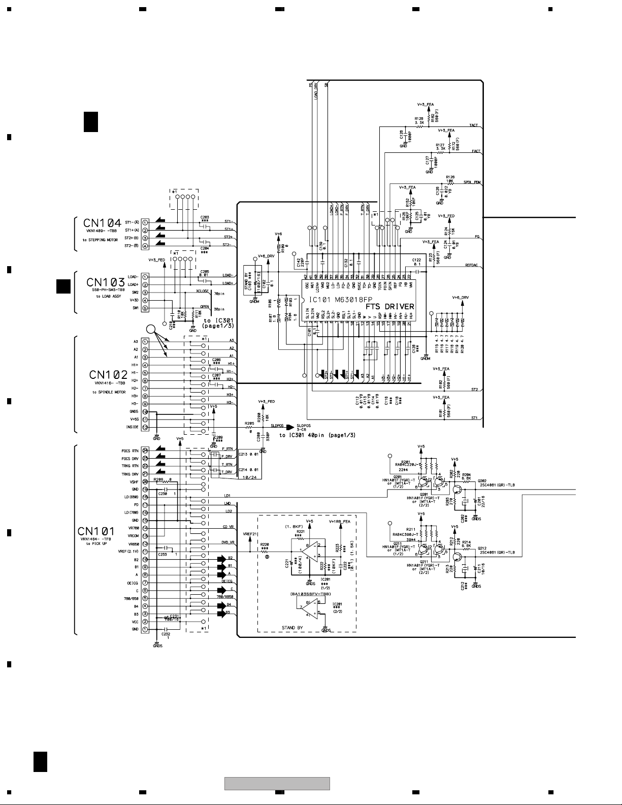
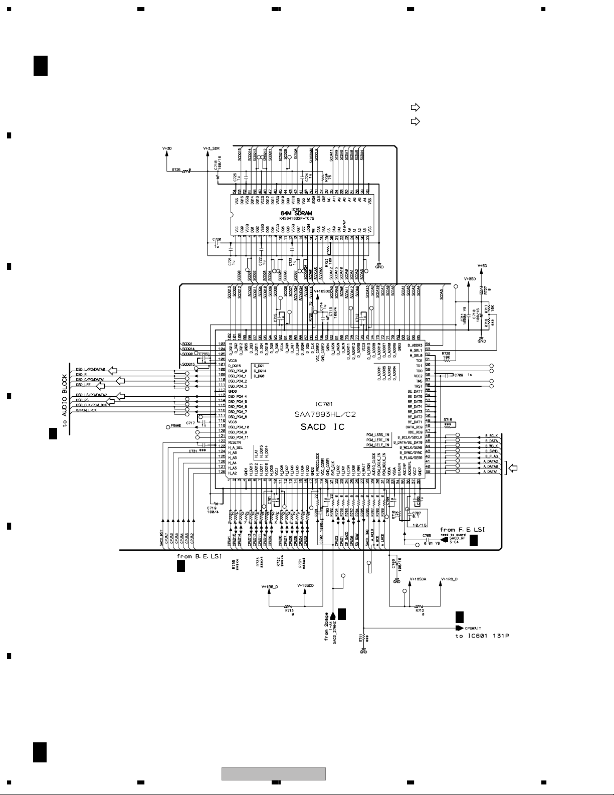
3.3 DVDM ASSY 1/3 [FRONT END BLOCK]
A
B 1/3
B
MOTOR
STEPPING
DVDM ASSY (VWS1563)
S
S
S
S
A
CN601
C
MOTOR
SPINDLE
5
SSS
S
F
F
D
ASSY-S
PICKUP
E
F
T
T
RF
RF
RF
RF
RF
RF
B 1/3
20
1234
DV-563A-S
Page 21
5 678
: RF SIGNAL ROUTE
RF
: FE_DATA SIGNAL ROUTE
F
: FOCUS SERVO LOOP LINE
T
: TRACKING SERVO LOOP LINE
S
: STEPPING SERVO LOOP LINE
A
1– 5: Refer to "3.10 WAVEFORMS".
B
3
B
2/3
C
4
D
2
1
B
3/3
RF
E
RF
DV-563A-S
56
F
B 1/3
7
8
21
Page 22
1234
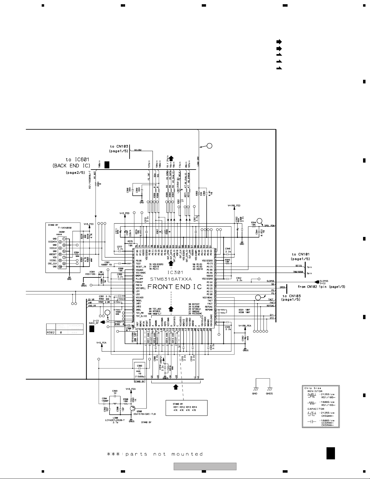
3.4 DVDM ASSY 2/3 [BACK END BLOCK]
A
B
C
B 2/3
DVDM ASSY (VWS1563)
B
3/3
D
E
F
B 2/3
22
B
1/3
B/Cb
G/Y
R/Cr
S-Y/Y
S-C/C
B/Cb
G/Y
R/Cr
V
S-Y/Y
S-C/C
V
D
AD
D
B
3/3
AD
DV-563A-S
1234
Page 23
5 678
A
: FE_DATA SIGNAL ROUTE
B
S-C/C
: V SIGNAL ROUTE
V
6.8
6.8
V
: S-VIDEO OUT C/C SIGNAL ROUTE
S-C/C
: S-VIDEO OUT Y/Y SIGNAL ROUTE
S-Y/Y
: R/Cr SIGNAL ROUTE
R/Cr
: G/Y SIGNAL ROUTE
G/Y
: B/Cb SIGNAL ROUTE
B/Cb
: AUDIO DATA SIGNAL ROUTE
AD
: AUDIO(DIGITAL) SIGNAL ROUTE
D
S-Y/Y
G/Y
B/Cb
R/Cr
6.8
D
6.8
6.8
R/Cr
D
V
S-C/C
S-Y/Y
G/Y
B/Cb
C
CN102
D
C 1/2
6.8
B
3/3
D
D
D
D
D
E
56
DV-563A-S
CN101
C 1/2
F
B 2/3
7
8
23
Page 24
1234
3.5 DVDM ASSY 3/3 [SACD and POWER SUPPLY BLOCK]
A
B
C
B 3/3
DVDM ASSY (VWS1563)
: AUDIO DATA SIGNAL ROUTE
AD
: AUDIO(DIGITAL) SIGNAL ROUTE
D
D
D
D
D
D
B
2/3
D
B
1/3
B
2/3
E
B
2/3
B
2/3
AD
F
B 3/3
24
1234
DV-563A-S
Page 25
5 678
A
B
: The power supply is shown with
the marked box.
D
CN104
C
D
E
F
CN101
B
2/3
B
2/3
56
DV-563A-S
F
B 3/3
7
8
25
Page 26
1234
3.6 JCKB ASSY 1/2 [AUDIO BLOCK]
A
B
C
C 1/2
S-C/C
S-Y/Y
R/Cr
G/Y
B/Cb
(VWV1942)
: V SIGNAL ROUTE
V
: S-VIDEO OUT C/C SIGNAL ROUTE
: S-VIDEO OUT Y/Y SIGNAL ROUTE
: R/Cr SIGNAL ROUTE
: G/Y SIGNAL ROUTE
: B/Cb SIGNAL ROUTE
: AUDIO(DIGITAL) SIGNAL ROUTE
D
: AUDIO SIGNAL ROUTE
CN601
B 2/3
JCKB ASSY
: The power supply is shown with
the marked box.
D
D
D
D
D
D
D
D
D
D
D
V
S-C/C
CN602
B 2/3
E
S-Y/Y
G/Y
B/Cb
R/Cr
C
2/2
V
S-C/C
S-Y/Y
G/Y
B/Cb
R/Cr
11
D
9
8
107
6
22/50
F
C 1/2
26
1234
DV-563A-S
Page 27
5 678
6– -: Refer to "3.10 WAVEFORMS".
A
B
C
330/10
330/10
D
C
2/2
E
F
56
DV-563A-S
C 1/2
7
8
27
Page 28
1234
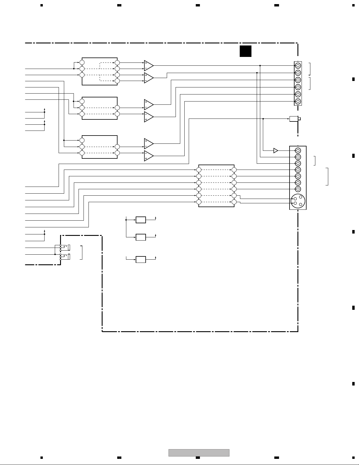
3.7 JCKB ASSY 2/2 [VIDEO BLOCK]
A
B
C
C 2/2
S-C/C
S-Y/Y
R/Cr
G/Y
B/Cb
(VWV1942)
: V SIGNAL ROUTE
V
: S-VIDEO OUT C/C SIGNAL ROUTE
: S-VIDEO OUT Y/Y SIGNAL ROUTE
: R/Cr SIGNAL ROUTE
: G/Y SIGNAL ROUTE
: B/Cb SIGNAL ROUTE
: AUDIO(DIGITAL) SIGNAL ROUTE
D
: AUDIO SIGNAL ROUTE
: The power supply is shown with
the marked box.
JCKB ASSY
C
1/2
V
S-C/C
S-Y/Y
G/Y
B/Cb
D
E
R/Cr
D D
V
S-C/C
S-Y/Y
G/Y
B/Cb
R/Cr
F
C 2/2
28
D
C
1/2
D
DV-563A-S
1234
Page 29
5 678
A
B
S-C/C
S-Y/Y
G/Y
B/Cb
R/Cr
C
V
12
17
16
14
15
13
S-C/C
C
V
S-Y/Y
1/2
D
D
G/Y
B/Cb
R/Cr
E
56
DV-563A-S
=– $: Refer to "3.10 WAVEFORMS".
C 2/2
7
8
F
29
Page 30
1234
3.8 FLKY and PWSB ASSYS
A
B
FLKY ASSY
D
(DV-563A-S: VWG2427)
(DV-50A: VWG2430)
C
used
Not used
D
E
F
D
30
1234
DV-563A-S
Page 31

5 678
DV-563A DV-50A
Not used
Not used
: The power supply is shown with
the marked box.
PWSB ASSY
E
(VWG2429)
A
B
C
B 3/3
CN105
FLKY ASSY
S102 : FL DIMMER
S103 : 41
S104 : ¡¢
S105 : 7
S106 : 8
S107 : 3
S109 : 0
S110 : RETURN
S111 : MENU
S112 : \
S113 : »
S114 : TOP MENU
S115 : ENTER
S116 : |
S117 : HOME MENU
S118 : «
PWSB ASSY
S101 : STANDBY ON
D
E
F
56
DV-563A-S
D E
7
8
31
Page 32

1234
3.9 POWER SUPPLY UNIT
A
B
CAUTION : FOR CONTINUED PROTECTION AGAINST RISK OF FIRE.
REPLACE ONLY WITH SAME TYPE NO. 491.800 MFD, BY
LITTELFUSE INC. FOR P301 (AEK7063).
CAUTION : FOR CONTINUED PROTECTION AGAINST RISK OF FIRE.
REPLACE ONLY WITH SAME TYPE NO. 49101.6 MFD, BY
LITTELFUSE INC. FOR P101 (AEK7066).
CN101
P101
AEK7066
CN401
1.6A
B 3/3
C
P301
800mA
AEK7063
D
E
POWER SUPPLY UNIT (VWR1365)
F
F
• In case of repairing, use the described parts only to prevent an accident.
• Please write the red mark on the board when the primary section of POWER SUPPLY (SYPS) Unit is repaired.
• Please take care to keep the space, not touching other parts when replacing the parts.
NOTE OF SPARE PARTS IN POWER SUPPLY (SYPS) UNIT
CN1
AC IN
F F
32
1234
DV-563A-S
FOR CONTINUED PROTECTION AGAINST RISK OF FIRE.
REPLACE WITH SAME TYPE AND RATINGS ONLY.
CAUTION -
• NOTE FOR FUSE REPLACEMENT
Page 33

5 678
3.10 WAVEFORMS
Note : The encircled numbers denote measuring point in the schematic diagram.
Measurement condition
: No. 1 to 2 and 12 to 17 : reference A1 (DVD), T2-chp 19, Color-bar
No. 6 to 11 : reference A1 (DVD), T2-chp 1
DVDM ASSY
B
IC301 - pin 99 [RF]
1
V: 200mV/div. H: 0.1µsec/div.
IC301 - pin 55 [LOAD_DRV]
3
V: 1V/div. H: 500nsec/div.
IC301 - pin 44 [SPDL_PDM]
4
GND
[Tray stops] [Tray is opening] [Tray is closing]
IC301 - pin 36 [FG]
2
V: 1V/div. H: 5msec/div.
[PLAY][PLAY→STOP→PLAY] [STOP]
CN102 - pin3, 2, 1
5
(IC101 - pin 14, 13, 12)
[FTS Driver -A1, A2, A3]
A
B
C
Brakes
JCKB ASSY
C
Foot of R208 (IC201 - pin 5)
6
[AUDIO DAC -MCLK]
V: 1V/div. H: 50nsec/div.
Foot of R206 (IC201 - pin 1)
8
[AUDIO DAC -LRCK]
V: 2V/div. H: 5µsec/div.
Foot of R735 (IC701 - pin 25)
13
[Component Video out -Y]
V: 1V/div. H: 10µsec/div.
Foot of R736 (IC701 - pin 23)
14
[Component Video out -Pb]
V: 2V/div. H: 10µsec/div.
Foot of R737 (IC701 - pin 21)
15
[Component Video out -Pr]
V: 2V/div. H: 10µsec/div.
Accelertar
GND
ON
Foot of R207 (IC201 - pin 2, 4)
7
[AUDIO DAC -BCK]
V: 2V/div. H: 200nsec/div.
Foot of R206 (IC201 - pin 1)
9
[AUDIO DAC -LRCK]
Foot of R207 (IC201 - pin 2, 4)
10
[AUDIO DAC -BCK]
Foot of R202 (IC201 - pin 3, 25)
11
[AUDIO DAC -DATA]
(Waveform of DATA is unsettled.)
V: 2V/div. H: 500nsec/div.
Foot of R734 (IC701 - pin 28)
16
[S Video out -Y]
V: 1V/div. H: 10µsec/div.
13
14
15
Foot of R732 (IC701 - pin 31)
17
[S Video out -C]
V: 1V/div. H: 10µsec/div.
ON
STOPPLAY PLAY
V: 2V/div. H: 1sec/div. V: 2V/div. H: 500nsec/div. V: 2V/div. H: 500nsec/div.
[PLAY]
V: 2V/div. H: 2msec/div.
D
Foot of R733 (IC701 - pin 33)
12
[Composite Video out]
9
10
11
V: 1V/div. H: 10µsec/div.
16
17
E
F
56
DV-563A-S
7
8
33
Page 34

1234
A
B
C
D
E
F
34
1234
DV-563A-S
Page 35

5 678
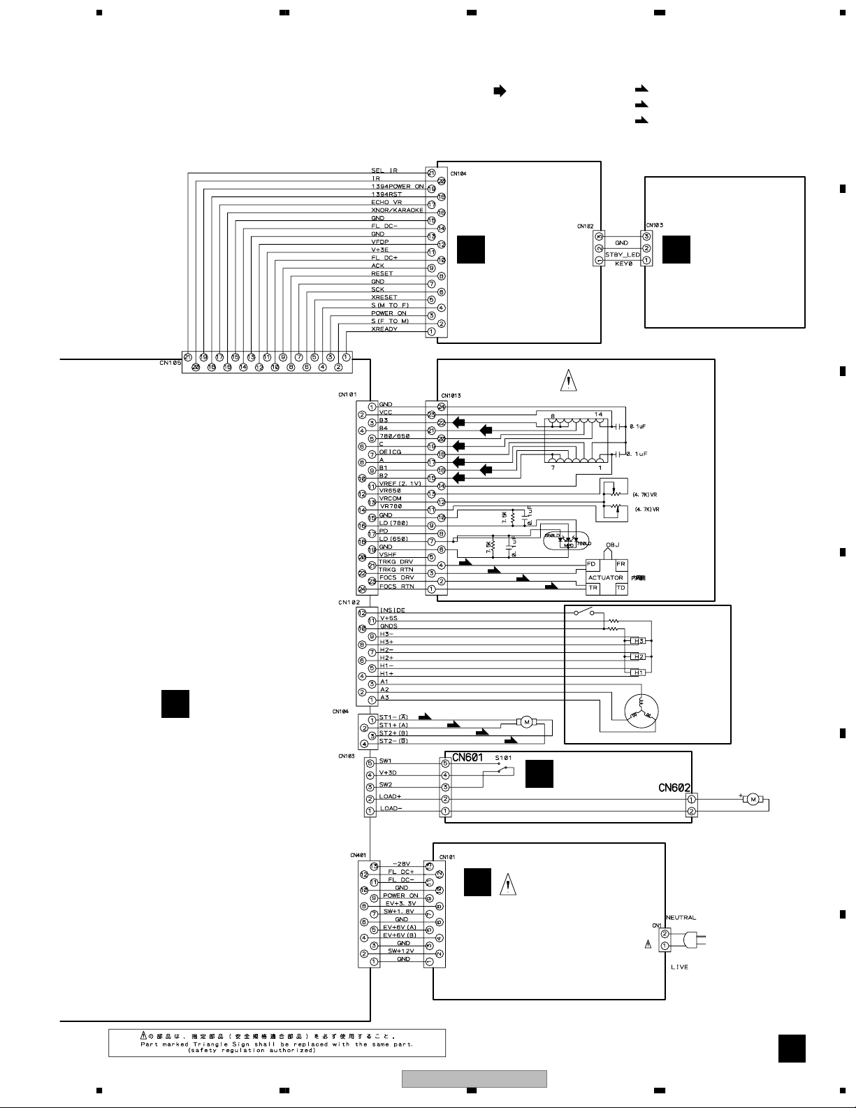
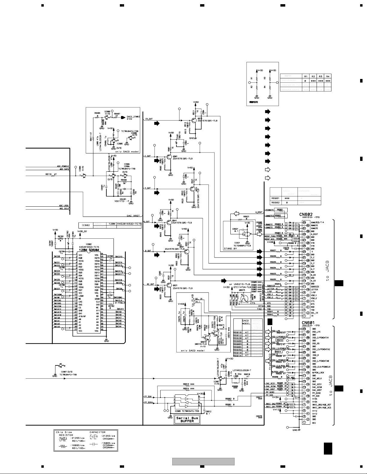
4. PCB CONNECTION DIAGRAM
4.1 LOAB ASSY
NOTE FOR PCB DIAGRAMS :
1. Part numbers in PCB diagrams match those in the schematic
diagrams.
2. A comparison between the main parts of PCB and schematic
diagrams is shown below.
Symbol In PCB
Diagrams
BCE
B
D
C
E
S
Symbol In Schematic
Diagrams
BCEB CE
S
BC
DG
BCE
DGG
Part Name
Transistor
E
Transistor
with resistor
S
Field effect
transistor
Resistor array
3. The parts mounted on this PCB include all necessary parts for
several destinations.
For further information for respective destinations, be sure to
check with the schematic diagram.
4. View point of PCB diagrams.
Connector
Capacitor
SIDE A
P.C.Board
Chip Part
SIDE B
A
B
3-terminal
regulator
SIDE A SIDE B
LOAB ASSY
A
(VNP1910-A)
CN602
12
LOAB
15
CN601
VWG
VNP1910-
5
VWG2426-
1
S101
PYKC F6
GND
51
C102
C101
(V+5D)
V+3D
SW2
51
CN601
LOAD+
LOAD-
CN602
12
CN601CN602 CN602CN601
CN103
B
M
LOADING
MOTOR
ASSY
C
D
E
F
AA
56
DV-563A-S
7
8
35
Page 36

1234
4.2 DVDM ASSY
SIDE A SIDE A
A
DVDM ASSY
B
(VNP1921-A)
CN601
R6916
C422
R6918
R6912
C
CN401
B
CN101
1
C406
CN601
33
SIDE
CONTACT
32
IC402
F
C408
PICKUP
ASSY
C230
SIDE
CONTACT
C
CN101
CN104
D
STEPPING
MOTOR
M
CN101
R206
24
SIDE
1
CONTACT
CN104
4
CN102
PRE FLUXHEAT PROOF
CN102
C103
SPINDLE
MOTOR
M
CN401
C430
13
R421
C410
2
1
C233
R220
23
C221
C390
C394
C392
L390
1
C393
R319
Q390
C209
C318
CONTACT
R120
C102
1
CN103
5
C319
C323
R119
KN102
C210
C303
C309
C315
R118
R390
12
C207
1
SIDE
R391
C206
E
7
IC401
C401
C231
C201
R393
R392
R302
C300
R300
100
25
26
C326
C302
R117
R115
R116
B
VWS1566
C411
C412
5
C716
41
C402
C211
X301
10
NP
C388
C391
C342
21
IC101
22
C122
C126
R126
R128
R6914
C713
C715
102
103128
C717
C731
1
R735
CN301
2
R733
9
1
C377
R374
76
C373
75
51
50
C344
C348
R344
IC301
C132
C128
R182
3
3
R425
R426
4
4
R428
VWS1565VWS1563
R6920
C424
R6922
C362
C139
1
515
C701
C101
C142
IC400
C
R6924
R732
1
10
C301
1
R6926
C360
R417
1
CN101
R6908
R6909
R6905
R6980
C712
C714
C703
C704
C702
C707
C708
R731
R6332
20
11
5
4
1
C6313
3
IC611
R361
L361
C357
C355
R355
C
B
A
42
R404
C6314
R6333
C6977
65
IC613
R6903
38
R707
R734
R6105
R6101
R736
C404
999
C710
R6904
6439
R737
R6106
888
C6978
DAC_MCK
R728
C709
R715
R706
C6122
R6159
777
R6039
R6982
R6981
1
2
R6053
R727
C711
IC701
A_MCLK
C6703
R6117
C6160
123456789
555
666
R6991
R405
1
R6984
C719
R6052
R6056
C6064
C6094
SACD_27M
C461
21
R6983
SIDE
CONTACT
C6048
C6047
R6993
R6104
0
444
R6997
R419
R6045
R6075
C6081
104
C6150
1
1
333
R406
CN602
33
32
C6049
C6037
52
53
105
C6119
R6118
C6107
1
2
SIDE
18
CONTACT
R6511
R6512
0
123
0
0
VWS1
000
111
222
R431
R407
R432
C462
A-
CN105
SIDE
CONTACT
VNP1921-
CN102
C
B_CB
R_CR
S_YVS_C
G_Y
C6001
C6050
C6976
R6123
R6124
CN603
R6529
R6502
R6501
DVDM(SECOND)
C6121
R6121
C6505
R6526
R6527
C6030
CN609
C6506
R6530
R6523
C6124
R6524
C6023
23
1
2
24
R6131
R6305
ADC_PCMCLK
R6525
R6528
C6503
R6141
R6308
C6508
R6943
C6014
C6136
CN602
C501
C6149
IC601
R6142
R6932
1
208
C6213
C6184
157
KN103
156
23
24
CN608
R6146
Q6302
4
6
SIDE A
1
2
R6032
C6015
C6198
C6159
3
C6171
R6156
R6152
1
R6301
D6301
R6303
D6971
R6033
R6183
29
1
R6031
C6004
30 2
R6191
R6302
R6304
R6309
Q6972
C6172
C6137
R6184
CN607
FC DC
2/2
R6211
R6001
R6149
R6187
A
CN103
CN105
CN104
D
CN601
A
Q390
IC402 IC701
IC401
IC101
IC400
IC613
IC601
IC611IC301
F
B B
36
1234
DV-563A-S
Q6302
Q6972
Page 37

5 678
SIDE B SIDE B
DVDM ASSY
B
(VNP1921-A)
R6939
R6901
R6974
R6976
C6974
Q6973
R6206
R6196
C6975
R6009
R6200
IC603
R6975
R6013
R6210
R6207
R6193
1
24
C6973
R6979
R6212
R6190
R6016
R6209
R6204
R6973
R6202
R6203
R6021
R6208
R6205
R6306
R6977
R6942
C6972
R6971
R6972
R6970
V+1R8_BE
Q531
R6213
R6020
C503
R6941
R533
R6978
C6901
R553
R531
R6167
R6163
D6502
C6902
C507
Q551
R552
C6502
C6511
C6904
C6903
R532
R6186
R6185
R6125
R6127
R6126
R551
R523
R543
C6512
R6936
R6934
C6905
R6935
R6933
C505
Q521
C504
R511
R522
R521
C506
R541
R503
R6028
R542
Q541
R6157
R6109
IC604
R6110
R6112
R6113
X6401
C6312
R6114
R6115
C6403
48
C6301
25
R6531
916
18
D6511
C6510
C6507
C6509
R6938
R6035
R6095
R6411
R513
C6401
1
4
IC615
R6937
Q511
C6707
C6708
L604
R6402
R6988
R6987
R6985
R6986
R512
R6921
C6921
C502
5
R501
IC621
1
Q501
R502
R6043
28
R6018
R6017
R6702
54
R6116
58
R6401
C6504
L657
1
4
IC606
R6522
R6521
R6520
R6907
4
3
R6047
R6042
R6046
C6057
C6404
C6906
5
IC607
R6404
C6908
C6907
4
R6405
C6402
R6055
8
5
85
R6814
1
1
8
R6812
C6809
R6996
L606
R6407
R6701
C6701
R436
SIDE B (FIRST)
C6812
C6808
R435
IC608
4
27
R434
R6813
1
R433
R6008
R6810
C6810
R709
C6702
L608
L607
R6073
R6072
R6071
R724
IC602
C6706
R427
R716
C6704
R6902
R725
R726
R708
C6705
R717
R710
27
R711
R6344
R6345
C6317
R6347
C6319
R6342
C6320
R2
R1
C409
R420
C718
28
C435
C720
R408
R723
R703
R430
R6343
R6322
R6323
R4
R3
C407
R6329
C423
C705
C311
R104
R411
R705
R702
C706
R6328
R107
R418
C420
R402
C723
R103
R380
C368
R437
C724
R701
R6325
R6324
C381
R106
R368
C451
R365
C400
IC702
C722
C725
R704
R378
R375
C369
R369
R367
R381
R364
R363
3
45
R400
C721
R382
R384
R379
R372
1
IC451
C425
1
54
SACD_RF
R383
R450
R752
R366
C114
R753
R754
R721
R751
R371
R345
V+12
C431
4
5
R424
R200
C432
R412
R713
C212
C124
R482
R203
Q202
C202
R124
R409
Q212
C413
R712
R394
R331
R213
R330
C112
132
R422
R480
R101
C113
R172
C405
IC403
C403
R488
R102
C116
R127
C433
R481
R222
R312
R311
R314
R313
C118
C127
C434
R423
R221
C120
C125
R403
R125
R413
4
5
C213
R152
R415
R442
C214
R444
R223
R310
R301
R205
C200
R123
C222
1
8
C232
Q403
IC201
C205
PC
R414
Q401
C204
R109
R110
R416
C429
C203
R441
R410
Q402
R212 R214
R204
R202
R111
C427
R401
R443
Q211
R211
Q201
R201
A
B
C428
C
D
E
Q6973 Q511Q521
Q531
IC603
Q541
IC615
Q501
IC604 IC606
IC607
IC602
IC608
IC702
IC451
Q212
Q211
Q201
Q402Q551
IC201
Q403
Q401
Q202
IC403IC621
B B
56
DV-563A-S
7
8
F
37
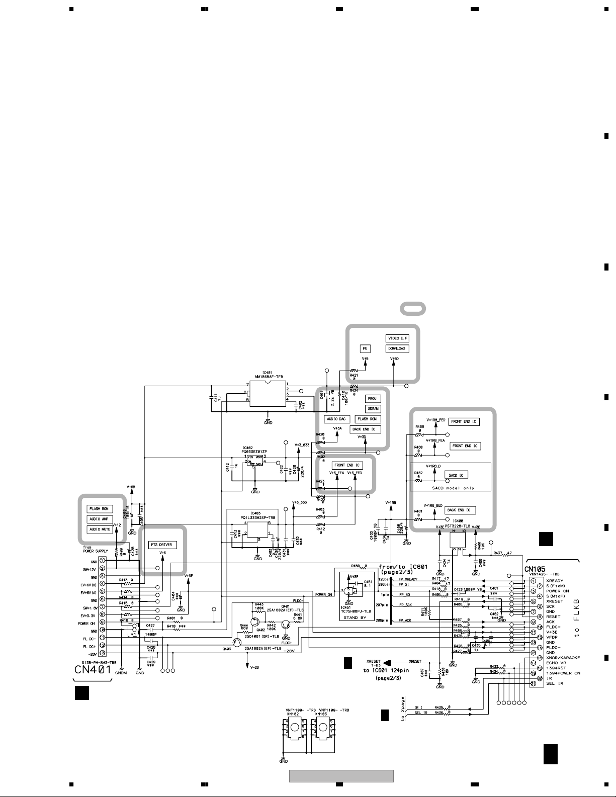
Page 38

1234
C106
4.3 JCKB ASSY
SIDE B
A
R644
17
R645
D601
C623
R621
R623
C624
C622
D706
D707
D708
D709
R622
C621
Q101
R752
B
IC103
IC104
IC204
Q702
Q401
Q301
Q402
Q302
Q751
R702
Q702
C738
R703
R601
R762
C755
C756
C753
C754
C601
C
B
A
Q751
R751
C752
C751
C737
C736
C117
C112
0
1
123
0
0
123456789
0
1
R743
R742
R738
R741
R739
R740
C136
R105
R136
R134
R135
1
C114
C115
8
IC104
C134
R714
R724
R717
C729
R715
L704
C132
R132
1
C101
L104
IC103
8
R102
C
D
E
SIDE A
IC401
IC301
IC102
IC201
IC771
IC701
IC101
IC751
IC302 IC402
IC801
Q203
Q202
Q201
Q214
Q216
Q215
Q204
Q801
Q303 Q403
Q210
Q404
Q305
Q206
Q207
Q205
Q304
Q405Q208
JCKB ASSY
C
(VNP1919-B)
33.IR
32.SEL_IR
31.TXD
33
30.RXD
29.RTS
28.CTS
27.VSEL2
26.VSEL1
32
25.I/XP
24.LETTER
23.SQUEEZE
21.CR/R
19.CB/B
R612
C734
C711
2
KN101
17
R610
R609
R611
C743
C742
R719
R718
D710
17.Y/G
15.Y
13.C
11.V
9.V+6
8.V+6
5.D_OUT
3.XAMUTE
2.XMMUTE
1.XAMUTE2
CN102
R607
CN102
R608
C706
C705
18
19
C710
R736
R735
R737
D704
D705
D703
CN601
R606
IC701
R734
D702
C704
R605
C703
R731
D701
R604
R602
C701
1
C709
R732
R733
D711
D712
CN602
B
R603
CONTACT SIDE
C702
C772
C774
C708
36
C707
PC
CN101
R613
1
2
C771
5
7
IC771
C761
4
1
C773
C768
C775
33
32
CONTACT SIDE
R199
R121
R120
C765
R614
R119
R118
R101
R116
R615
C762
C766
18
C764
JA602
1
R115
IC751
R112
C111
B
R110
R111
1936
CN601
1
2
R108
R109
CN101
C732
C763
C767
JA601
R106
30.V+12
29.V+12
26.V+3A
25.V+3A
24.FP_SO
23.FP_SCK
22.DAC_RST
21.DAC_XCS0
R107
1
18.A_MCK
16.0/PCM_LRCK
14.DSD_CLK/PCM_BCK
12.DSD_L/PCMDATA0
10.DSD_R
8.DSD_LS/PCMDATA2
6.DSD_RS
4.DSD_C/PCMDATA1
2.DSD_LFE 20.DAC_XCS1
JCKB ASSY
CMKD-P3X
C110
3
CN701
R104
R133
L101
V+3D
V+12A
V+5V
C726
FCDC
KN102
F
C
38
1234
DV-563A-S
Page 39

5 678
C
KN102
SIDE B
R714
R724
C729
R715
C132
R105
R135
R132
1
C114
C115
L104
8
I
IC103
R102
R716
R717
L704
R713
L703
R712
R131
1
C106
C101
L103
8
C133
R723
C727
C728
R711
C107
V+12A
R809
R808
R806
C806
R804
C802
C803
R805
R705
C714
R707
C210
R771
R209
V+5V
C103
V+12A
V+3D
R201
C716
C717
R706
C104
V+5A
R114
D101
C124
T-VWV389
prodaction
Trial
C123
C122
R704
C108
C715
D102
R113
JCKB
C721
R708
C212
C113
VWM
ASSY
R710
L702
R248
R239
R247
R237
R211
R210
-A1
111
000
C723
R709
R722
L701
C248
R235
C247
Q101
333
222
C722
R244
R243
R240
555
444
C254
R721
4
5
777
666
R263
R261
1
C231
8
R233
R232
999
888
C255
C253
R259
R257
R241
R236
IC204
VREF
V+5A
C252
C334
R255
R346
R265
R254
R264
R328
V+12A
R316
R310
C303
C306
R345
R341
R344
R327
Q302
Q301
R315
C433
C434
C333
R446
R428
R362
R361
R416
R410
C406
C403
R445
R444
R441
R427
Q402
Q401
R415
A
B
C
CMKD-P3X
R133
C110
L101
V+3D
V+12A
V+5V
CN701
SIDE A
WARNING
THIS PRODUCT CONTACT LEAD IN SOLDER AND CERTAIN ELECTRICAL PARTS CONTAIN
CHEMICALS WHICH ARE KNOWN TO THE STATE CALIFORNIA TO CAUSE CANCER,
BIRTH DEFECTS OR OTHER REPRODUCTIVE HARM. WASH HANDS AFTER HANDLING.
HEALTH & SAFETY CODE SECTION 25249.6 - PROPOSITION 65
CONTACT SIDE
19.B
18.R
17.VSEL2
16.G
R104
6.SQUEEZE 14.Y
4.AUDIO_R
12.C
2.AUDIO_L
10.V
1.V+12V
8.V+5V 15.VSEL1
78M05
C730
C102
IC101
R202
R206
R207
C809
R803
C805
R802
C724
C725
C726
Q801
L801
R811
C801
5
C807
1
C808
JA801
TZ
IC801
L802
R812
19
CN751
Q214
C731
C735
R205
R204
R281
R203
C207
1528
C733
1
IC201
R212
R208
114
C202
C204
C211
C105
R801
C804
R892
R807
C206
C201
C713
IC102
C208
C209
C119
R272 Q202
R280
R273
C118
C109
C203
C205
C116
C712
R274
Q203
R271
R282
R283
Q201
Q215
R231
R234
C234
C236
Q216
C242
C238
C240
C244
R238
R242
C718
C720
JA102
C719
R267
Q210
Q207
R260
C135
R305
R307
C322
C245
Q208
R308
R253
R325
110
C301
R322
R326
R251
Q205
R306
R304
R309
20
IC301
C308
11
C305
C304
C321
C324
C326
C325
8
C328
C329
C332
R256
Q305
R408
R407
R406
110
C401
C422
C424
C428
R342
Q405
R405
20
R409
IC401
11
C405
C404
C408
C426
C425
8
C429
C430
C432
R364
Q404
R443
C402
C407
R363
R422
R321
C323
R324
1
IC302
R323
C327
R426
R425
C330
C331
Q303
Q304
R343
C131
C121
C302
C307
C232
Q204
C246
R262
R266
Q206
R258
R404
C423
1
IC402
C427
R442
R424
R423
R461
C431
Q403
R464
JA101
2/2
5
R463
C421
R421
R462
4
KN103
D
E
56
DV-563A-S
F
C
7
8
39
Page 40

1234
4.4 FLKY and PWSB ASSYS
SIDE A
A
D
CN102
CN102
B
FLKY ASSY
(VNP1901-B)
12
3
13
D101
PYKC F4X
D102
S102
FL DIM
C
D
VWG2425VWG2424-
PWSB
PWSB ASSY
E
(VNP1901-B)
SIDE B
PWSB ASSY
E
(VNP1901-B)
R138
K
PWSB
VWG2424VWG2425-
C154
3
12
13
CN103
PYKC F4X
D105
POWER
S101
CN103
J
CN103
13
CN103
S103
D104
S104
>>
<<
C
R155
R156
R137
FL101
D
R158
R191
R192
R193
R194
8
9
766
8
9
7
55
9
8
5
7
6
VWG2
1
4
0
1
33
22
0
4
1
4
3
2
0
1
-A
E
F
D E
40
R154
B
R133
13
CN102
CN102
FLKY ASSY
D
(VNP1901-B)
DV-563A-S
1234
Page 41

5 678
1
IR101
VNP1901-
DC FC
STOP/EJECT
S109
EJECT
S105
PC
L101
C181
PAUSE/<<
S106
C101
X101
VWG
FLKY
PLAY/>>
S107
VWG2417VWG2418-
VWG2419VWG2420-
S108
1
1
CN101
CN104
VWG2421VWG2422VWG2423-
/STOP
CN104
TOP MENU
S117
21
21
S114
S116
HOME MENU/PAUSE
CN105
B
LEFT
SIDE A
A
1
UP
S113
S115
ENTER
S118
DOWN
RIGHT
/PLAY
S119
S112
RETURN
MENU
S110
S111
B
C
SIDE B
D
CN104
C157
R104
1
CN101
R110
R187
R135
R185
R172
R189
R111
R173
R105
C102
R183
CN101CN104
R199
C155
R107
R109
R121
R112
I
R103
R167
R136
R140
R184
21
R131
C183
R123
R166
R122
R198
C152
R120
R125
R168
R126
R165
R127
R128
R129
R159
R130
F
R160
R164
R163
R161
R162
C151
R153
R170
R169
G
H
E
C104
R195
C103
R134
R196
C159
61 80
R181
R197
61 80
A
IC101
C199
VWG2
4
33
22
001
55
4
11
5
4
0
3
2
1
-A
C106
R182
C182
VNP1901-
VWG2423-
VWG2422-
VWG2421VWG2420VWG2419VWG2418VWG2417-
R151
FLKY
C153
E
R152
R139
C184
C156
R186
R188
R190
C158
41 60
40
41 60
R108
R106
21
21 40
20
20
R171
R124
C105
1
1
R132
56
DV-563A-S
F
D
7
8
41
Page 42

1234
4.5 POWER SUPPLY UNIT
SIDE A SIDE B
A
POWER SUPPLY UNIT
F
AC IN
CN1 CN1
B
[VWR1365]
C
P301
D
P101
E
CN401
B
CN101
F
F F
42
1234
DV-563A-S
Page 43

5 678
5. PCB PARTS LIST
NOTES:
Parts marked by "NSP" are generally unavailable because they are not in our Master Spare Parts List.
The mark found on some component parts indicates the importance of the safety factor of the part.
Therefore, when replacing, be sure to use parts of identical designation.
When ordering resistors, first convert resistance values into code form as shown in the following examples.
Ex.1 When there are 2 effective digits (any digit apart from 0), such as 560 ohm and 47k ohm (tolerance is shown by J=5%,
and K=10%).
560 Ω
47k Ω
0.5 Ω
1 Ω
56 x 10
47 x 10
R50
1R0
1
3
Ex.2 When there are 3 effective digits (such as in high precision metal film resistors).
5.62k Ω
1
Mark No. Description Part No.
LIST OF ASSEMBLIES
[DV-563A-S]
NSP 1..LOADING MECHA. ASSY VWT1207
NSP 2..LOAB ASSY VWG2426
1..DVDM ASSY VWS1563
1..JCKB ASSY VWV1942
NSP 1..FLKB ASSY VWM2184
2..FLKY ASSY VWG2427
NSP 2..PWSB ASSY VWG2429
1..POWER SUPPLY UNIT VWR1365
>
[DV-50A]
NSP 1..LOADING MECHA. ASSY VWT1207
NSP 2..LOAB ASSY VWG2426
1..DVDM ASSY VWS1563
1..JCKB ASSY VWV1942
NSP 1..FLKB ASSY VWM2191
2..FLKY ASSY VWG2430
NSP 2..PWSB ASSY VWG2429
1..POWER SUPPLY UNIT VWR1365
>
Mark No. Description Part No.
LOAB ASSY [VWG2426]
A
SWITCHES AND RELAYS
S101 REAF SWITCH VSK1011
561
473
5621
RD1/4PU J
RD1/4PU J
RN2H K
RS1P K
RN1/4PC F562 x 10
561
473
R50
1R0
5621
Mark No. Description Part No.
IC402 PQ033EZ01ZP
>
IC403 PQ1L333M2SP
>
IC400 PST3228
IC701 SAA7893HL/C2
IC601 STI5588CVB
IC301 STM6316ATXXA
IC608 TC7WH34FU
IC604, IC606, IC607 TC7WU04FU
IC603 VYW2087
Q390, Q501, Q511, Q521, Q531 2SA1576A
Q541, Q551 2SA1576A
Q401, Q403 2SA1602A
Q202, Q212, Q402 2SC4081
Q6973 DTC114TUA
Q201, Q211 IMT1A
Q6302 UMD3N
Q6972 UMX1N
D6971 1SS355
D6301 RB501V-40
COILS AND FILTERS
L390 LCYA2R7J2520
L604, L606, L607 LCYA470J2520
L608 LCYAR22J2520
CAPACITORS
C309, C315, C318, C319, C323 CCG1179
C326, C342, C348, C357, C360 CCG1179
C373, C377, C388, C391, C6004 CCG1179
C6014, C6047, C6808 (2.2uF/6.3V) CCG1179
C390 CCSRCH180J50
C142 CCSRCH221J50
C200 CCSRCH331J50
C392 CCSRCH560J50
C393 CCSRCH7R0D50
C6402, C6403 CCSRCH8R0D50
A
B
C
D
E
OTHERS
CN602 CONNCTOR S2B-PH-K
CN601 CONNCTOR S5B-PH-K
PRINTED CIRCUIT BOARD VNP1910
DVDM ASSY [VWS1563]
B
SEMICONDUCTORS
IC602 K4S281632D-TC75
IC702 K4S641632F-TC75
IC101 M63018FP
IC401 MM1565AF
>
56
DV-563A-S
C211 CEVW100M16
C231, C406, C410, C501, C706 CEVW101M16
C710, C718 CEVW101M16
C6015, C6122, C713, C719 CEVW101M4
C201 CEVW220M16
C301, C408, C420, C430 CEVW221M4
C6049, C6050, C6137, C6160 CEVW221M4
C401 CKSQYB225K10
C127, C128, C381, C423, C427 CKSRYB102K50
C433, C6701, C702, C711 CKSRYB102K50
C112–C114, C124, C125, C205 CKSRYB103K50
7
8
F
43
Page 44

1234
Mark No. Description Part No.
C213, C214, C355, C705 CKSRYB103K50
C101, C102, C122, C132, C139 CKSRYB104K16
A
B
C300 CKSRYB104K16
C394 CKSRYB152K50
C126, C344 CKSRYB223K50
C403, C409, C6301, C6812, C707 CKSRYF104Z25
C230, C232, C233, C411, C412 CKSRYF105Z10
C424, C434, C435, C502–C507 CKSRYF105Z10
C6023, C6030, C6037, C6048, C6064 CKSRYF105Z10
C6081, C6094, C6107, C6119, C6121 CKSRYF105Z10
C6124, C6136, C6149, C6150, C6159 CKSRYF105Z10
C6171, C6172, C6184, C6198, C6401 CKSRYF105Z10
C6404, C6703-C6708, C6974, C6975 CKSRYF105Z10
C701, C703, C704, C708, C709 CKSRYF105Z10
C712, C714–C717, C720–C725 CKSRYF105Z10
RESISTORS
R6017, R6932 RAB4C0R0J
R201 RAB4C220J
R211 RAB4C390J
R109, R402, R403, R408, R409 RS1/10S0R0J
R412–R416, R420, R421, R424 RS1/10S0R0J
R427, R480–R482, R488, R6149 RS1/10S0R0J
R6159, R6305, R6701, R712, R713 RS1/10S0R0J
C
D
R725, R727 RS1/10S0R0J
R103, R106 RS1/10S1R0J
R104, R107 RS1/10S1R8J
R115–R120 RS1/10S4R7J
R125, R152, R330, R331, R6028 RS1/16S1002F
R6035 RS1/16S1002F
R301 RS1/16S1202F
R502, R512, R522, R532, R542 RS1/16S1500F
R552 RS1/16S1500F
R101, R102, R123, R172, R182 RS1/16S5600F
Other Resistors RS1/16S###J
OTHERS
CN401 PH CONNECTER(SMT) S13B-PH-SM3
CN103 PH CONNECTER(SMT) S5B-PH-SM3
FLEXIBLE CABLE VDA1681
CN104 4P CONNECTOR VKN1409
CN102 12P CONNECTOR VKN1416
Mark No. Description Part No.
Q205–Q208, Q304, Q305 2SD2114K
Q404, Q405 2SD2114K
Q201, Q202, Q214, Q215 DTC114YUA
Q301, Q302, Q401, Q402, Q702 DTC114YUA
D101, D601 1SS355
D102 UDZS6.2B
COILS AND FILTERS
L701, L702 CHIP BEADS VTL1089
L801 CHIP BEADS VTL1108
CAPACITORS
C327, C328, C427, C428 CCSRCH151J50
C206, C303, C403 CCSRCH331J50
C621, C624 CCSRCH470J50
C302, C308, C321, C322, C402 CEAT101M10
C408, C421, C422 CEAT101M10
C232, C330, C430 CEAT101M16
C712, C713, C718 CEAT102M6R3
C205 CEAT220M50
C109, C116, C201, C203, C304 CEAT331M10
C404 CEAT331M10
C245, C246, C331, C332 CEAT470M16
C431, C432 CEAT470M16
C719, C720 CEAT471M6R3
C102, C118, C732, C771 CEJQ101M16
C804 CEJQ1R0M50
C105, C111, C707, C711, C730 CEJQ221M6R3
C743, C774, C805 CEJQ221M6R3
C702–C706, C773 CKSQYB225K10
C701 CKSQYF104Z25
C117, C202, C210, C212, C301 CKSRYB102K50
C401, C734, C737 CKSRYB102K50
C323, C324, C423, C424 CKSRYB152K50
C204, C207–C209, C231, C305 CKSRYF104Z25
C329, C405, C429, C714, C801 CKSRYF104Z25
C806 CKSRYF104Z25
C101, C106, C108, C112–C115 CKSRYF105Z10
C211, C247, C248, C306 CKSRYF105Z10
C325, C326, C406, C425, C426 CKSRYF105Z10
C623, C708–C710, C731, C733 CKSRYF105Z10
C736, C742, C772 CKSRYF105Z10
CN105 21P CONNECTOR VKN1425
CN101 24P CONNECTOR VKN1464
CN601, CN602 33P CONNECTOR VKN1519
KN102 EARTH METAL FITTING VNF1109
E
KN103 EARTH METAL FITTING VNF1109
X6401 (27MHz) VSS1172
X301 (20MHz) VSS1186
JCKB ASSY [VWV1942]
C
SEMICONDUCTORS
IC204, IC302, IC402 BA4560F
IC301, IC401 DSD1702EG
IC201 DSD1791DBR
IC701 LA73054
IC771 MM1565AF
>
F
IC101 NJM78M05FA
>
IC103, IC104 TC7WU04F
Q203, Q216, Q303, Q403 2SA1576A
Q101, Q801 2SC4081
44
C234, C236 CQMBA152J50
C238, C240, C242, C244 CQMBA561J50
RESISTORS
R323, R326, R423, R426 RN1/16SE1502D
R231, R234, R238, R242 RN1/16SE1801D
R232, R237, R239, R244 RN1/16SE3301D
R321, R322, R421, R422 RN1/16SE8201D
R271, R282, R361, R461 RS1/10S332J
R706, R707 RS1/10S68R0F
R324, R325, R424, R425 RS1/16S1001F
R233, R235, R240, R243 RS1/16S6800F
R704, R708–R710 RS1/16S68R0F
R805 RS1/16S75R0F
Other Resistors RS1/16S###J
OTHERS
JA801 OPT. LINK OUT 12MB/S GP1FA502TZ
JA601, JA602 JACK RKN1004
JA101 JACK VKB1167
DV-563A-S
1234
Page 45

5 678
Mark No. Description Part No.
JA102 JACK VKB1179
CN601 7P CONNECTOR VKN1211
CN101, CN102 33P CONNECTOR VKN1519
KN101–KN103 EARTH METAL FITTING VNF1084
FLKY ASSY [VWG2427]
D
SEMICONDUCTORS
IC101 PE5374A
D102 SLR-343VC
SWITCHES AND RELAYS
S102–S107, S109–S118 ASG7013
CAPACITORS
C183, C199 CKSRYB102K50
C151–C153 CKSRYB103K50
C102, C105 CKSRYF104Z25
C104 CKSRYF104Z50
C182 CKSRYF105Z10
RESISTORS
All Resistors RS1/16S###J
OTHERS
CN102 CONNECTOR POST B3B-PH-K
IC104 REMOTE RECEIVER RPM7240-H4
V101 FLUORESCENT TUBE VAW1078
CN104 21P CONNECTOR VKN1225
X101 (5MHz) VSS1142
Mark No. Description Part No.
P301 PROTECTOR(800mA) AEK7063
>
P101 PROTECTOR(1.6A) AEK7066
>
A
B
C
FLKY ASSY [VWG2430]
D
SEMICONDUCTORS
IC101 PE5374A
D102 SLR-343VC
SWITCHES AND RELAYS
S102–S107, S109–S118 ASG7013
CAPACITORS
C183, C199 CKSRYB102K50
C151–C153 CKSRYB103K50
C102, C105 CKSRYF104Z25
C104 CKSRYF104Z50
C182 CKSRYF105Z10
RESISTORS
All Resistors RS1/16S###J
OTHERS
CN102 CONNECTOR POST B3B-PH-K
IC104 REMOTE RECEIVER RPM7240-H4
V101 FLUORESCENT TUBE VAW1078
CN104 21P CONNECTOR VKN1225
X101 (5MHz) VSS1142
PWSB ASSY [VWG2429]
E
SWITCHES AND RELAYS
S101 ASG7013
D
E
OTHERS
CN103 CONNECTOR POST B3B-PH-K
POWER SUPPLY UNIT [VWR1365]
F
OTHERS
56
DV-563A-S
F
7
8
45
Page 46

1234
6. ADJUSTMENT
6.1 ADJUSTMENT ITEMS AND LOCATION
A
Adjustment Items
Adjustment Points (Mechanism Part)
[Mechanism Part]
1
Tangential and Radial Height Coarse Adjustment
2
DVD Jitter Adjustment
[Electrical Part]
Electrical adjustments are not required.
B
C
Cautions: After adjustment, adjustment screw locks with the
Screw tight.
1 2
Tangential
adjustment
screw
1 2
Radial
adjustment
screw
D
6.2 JIGS AND MEASURING INSTRUMENTS
E
F
Screwdriver (large)
Precise screwdriver
Screwdriver (medium)
DVD test disc
(GGV1025)
TV monitor
Soldering iron
Test mode remote control
unit (GGF1381)
Screw tight
(GYL1001)
46
1234
DV-563A-S
Page 47

5 678
6.3 NECESSARY ADJUSTMENT POINTS
When Adjustment Points
Exchange Parts of Mechanism Assy
A
Exchange the Pickup
Exchange the Traverse Mechanism
Exchange the Spindle Motor
Exchange PCB Assy
Exchange PC Board
LOAB and DVDM ASSYS
Mechanical
point
Electric
point
Mechanical
point
Electric
point
Mechanical
point
Electric
point
Mechanical
point
Electric
point
~, Ÿ
Ÿ
∗ After adjustment, screw locks
with the Screw tight.
B
∗ After adjustment, screw locks
with the Screw tight.
C
D
E
F
56
DV-563A-S
7
8
47
Page 48

1234
6.4 TEST MODE
A
• The TEST MODE functions that are used only during adjustment are described here. For details, see "7.1.1 TEST MODE".
TEST MODE: ON
ESC TEST
POWER
GGF1381
Test mode
B
ON
remote control
unit
TEST MODE: DISC SET
<TRAY OPEN>
OPEN/CLOSE
(Player)
C
DVD disc
TEST MODE: PLAY
<PLAY>
TV/LDP
D
< When playback with the target address of disc (DVD)>
For example, when playback with # 30000
An address is displayed
CHECK
DVD, CD
OPEN/CLOSE
(Player)
DSC - &&&
CAUTION:
Perform only trace, video and audio outputs
are nothing.
During PLAY
E
TEST MODE: OFF
POWER
F
48
+10 3 0 0 0 0 CHP/TIM
ESC
Press keys in order
030000
OR
GGF1381
Test mode
OFF
1234
remote control
unit
DV-563A-S
Page 49

5 678
6.5 MECHANISM ADJUSTMENT
Tangential and Radial Height Coarse Adjustment
1
A
START
• Remove the Loading Mecha. Assy.
• Remove a Spacer for height adjustment
attached to the back side (shaded area)
of the Loading Mecha. Assy (Float Base)
with nippers.
Loading Mecha. Assy
Float Base
Spacer for Height adjustment
Note:
Before removing the flexible cable for the
pickup, soldering of the pickup circuit is
necessary.
For details, see "7.1.10 DISASSEMBLY".
Cautions:
Because there is not a Spacer for height adjustment in
adjustment after the second time, will keep it at need.
(This parts is Traverse mechanism exclusive use of a model
for 2003 years)
7.3mm
Put a spacer between a Tangential (or Radial) adjustment
screw and Mechanism Base and turn each screw to adjust
the height. (Refer to "6.1 ADJUSTMENT ITEMS AND
LOCATION".)
Turn a flat side
into bottom
B
C
D
E
F
56
DV-563A-S
7
8
49
Page 50

1234
DVD Jitter Adjustment
2
A
• Playback method of inner and outer address for the purpose is refererd to "6.4 TEST MODE".
• Jitter indication of the monitor is refererd to "7.1.2 DISPLAY SPECIFICATION OF THE TEST MODE".
Use disc: GGV1025
START
• Test mode
• Play the DVD test disc
at outer track
(around #200000)
B
C
Mechanism Assy
Adjust the Tangential
Adjustment Screw so that
jitter becomes minimum.
J : Min
• Play the DVD test disc
at inner track
(around #30000)
Mechanism Assy
Adjust the Radial
Adjustment Screw so that
jitter becomes minimum.
J : Min
J : - - - -
Player
Monitor
D
CHECK
Turn the POWER OFF in
case of NG once, and
perform the adjustment
once again.
E
If error rate is OK,
locks a root of
tangential and radial
adjustment screws with
the Screw tight.
NG
Confirm the error rate that is
displayed "OK"
(Example ERROR RATE: 6.6oe - 6 OK )
OK
Disc playback normally.
• The measurement of block error rate
5ESC
• Play the DVD test disc
at outer track
(around #200000)
Mechanism Assy
Readjust the Tangential
Adjustment Screw so that
jitter becomes minimum.
J : Min
ESC
Screw tight: GYL1001
Test mode end
F
50
1234
DV-563A-S
Page 51

5 678
7. GENERAL INFORMATION
7.1 DIAGNOSIS
7.1.1 TEST MODE
Test Mode Functional Specification
1 Test mode entry
In the power ON state, press the [ESC] (A8-5F) key and [TEST / RANDOM] (A8-5E) key in order of the Test mode remote control
unit.
• Light the all FL and LEDs, and goes out the FL and LEDs when pressing the keys of something.
• OSD displays test mode. Refer to the "7.1.2 DISPLAY SPECIFICATION OF THE TEST MODE".
2 Release the Test mode
• Turn off the power.
• Press the [ESC] (A8-5F) key of the remote control unit and reset it.
3 Tray open / close
• Press the [REPEAT A-B] (A8 - 48) key of the remote control unit.
• Press the [OPEN / CLOSE] key of the main unit from the stop state.
4 Playback stop
1. Press the [REPEAT] (A8 - 44) key of the remote control unit from the playback state.
2. Press the [STOP] key of the remote control unit or main unit from the playback state.
(Playback stops, but the loaded disc keeps rotating.)
A
B
5 LD ON
DVD : Press the [TEST] (A8-5E) and [1] (A8-01) keys in order, and turn on the laser diode (650n).
CD : Press the [TEST] (A8-5E) and [4] (A8-04) keys in order, and turn on the laser diode (780n).
6 Focus on / sweep
1. Lock the focus by pressing the [TEST] (A8-5E) and [2] (A8-02) keys in order.
2. Repeat focus sweep by pressing the [TEST] (A8-5E) and [3] (A8-03) keys in order.
7 Spindle FG servo
CAV : Press the [TEST] (A8-5E) and [5] (A8-05) keys in order,then rise up the spindle and FG servo becomes on.
CLV : Press the [TEST] (A8-5E) and [9] (A8-09) keys in order,then rise up the spindle and FG servo becomes on.
8 Tracking open / close
1. Open tracking by pressing the [STEP FWD] (A8-54) key of the remote control unit in the play state.
2. Close tracking by pressing the [STEP REV] (A8-50) key of the remote control unit in the play state.
9 Slider servo on/off
1. Turn on the slider servo by pressing the [TEST] (A8-5E) and [CX] (A8-0E) keys in order.
2. Turn off the slider servo by pressing the [TEST] (A8-5E) and [TV/LDP] (A8-0F) keys in order.
0 Slider in / out
Slider in : In the tracking off state, press the [SCAN REV] (A8-11) key of the remote control unit.
Slider out : In the tracking off state, press the [SCAN FWD] (A8-10) key of the remote control unit.
- Play (perform only the ID search and trace to the specified location)
Press the [TV/LDP] (A8-0F) key of the remote control unit from the stop state.
Perform only trace, video and audio outputs are nothing.
C
D
E
= Screen display ON/OFF
1. Turn off the display by pressing the [AUDIO] (A8-1E) key of the remote control unit.
2. Turn on the display by pressing the [DISPLAY] (A8-43) key of the remote control unit.
DV-563A-S
56
F
7
8
51
Page 52

A
B
1234
~ Search
1. Search address input entry
• It becomes the address input mode when pressing the [+10] (A8-1F) key. (Most significant digit of an address displays "<".)
• In this time, display the last address as the initial state.
2. Search address input
• Press the [0] to [9] (A8-00 to 09) keys of the remote control unit. In the DVD, set an address with hexadecimal.
• In the address input mode, turn to the hexadecimal input by pressing the [PROGRAM] (A8-4C) key (display a "∗" mark), and [1] to
[6] keys are each input as A to F.
• Hexadecimal input and decimal input can switch with toggle.
• In case of CD, perform only the absolute time search.
3. Search execution
• Press the [CHP/TM] (A8-13) key of the remote control unit.
• After the search, perform only trace and video and audio outputs are nothing.
4. Release the Search address input
• Clear the address by pressing the [CLEAR] (A8-45) key. Release the address input mode when pressing the [CLEAR] key once again.
C
D
E
F
52
1234
DV-563A-S
Page 53

5 678
7.1.2 DISPLAY SPECIFICATION OF THE TEST MODE
Character in bold : Item name
: Information display
1
5
6
13
10
11
1 Address indication
The address being traced is displayed in number.
(as for the DVD, indication of decimal number is possible.)
DVD : ID indication (hexadecimal number, 8 digits)
[∗ ∗ ∗ ∗ ∗ ∗ ∗ ∗]
CD : A-TIME (min. sec.) [0 0 0 0 ∗ ∗ ∗ ∗]
2 Code indication of remote control unit [R – ∗ ∗ ∗ ∗]
In case of double code, display a 2nd code.
2
3
7
8
9
12
14
15
16
17
18
19
0 Disc sensing [DSC – ∗ ∗ ∗]
The type of discs loaded is displayed.
[DVD], [CD ], [VCD], [ ]
- Jitter value [J – ∗ ∗ ∗ ∗]
= Version of the AV-1 chip / version of firmware
[AV: ∗ ∗ / ∗ ∗ ∗ ∗ ∗ ∗ ∗ ∗]
A
B
C
3 Main unit keycode indication [K – ∗ ∗]
5 Tracking status [TRKG – ∗ ∗ ∗]
Tracking on : [ON]
Tracking off : [OFF]
6 Spindle status [SPDL – ∗ ∗ ∗]
[OFF], [ACC/BRK], [CAV], [CLV]
7 Mechanism (loading) position value [M – ∗ ∗]
Unknown : [01] or [41]
Open state : [04]
Close state : [08]
During opening : [12]
During closing : [22]
8 Slider position [S – ∗ ∗ ∗ ∗]
In Side Switch ON : [01]
In Side Switch OFF : [00]
9 Output video system [V – ∗ ∗ ∗ ∗]
NTSC system : [NTSC]
PAL system : [PAL]
Automatic setting : [AUTO]
Scart terminal output [SK – ∗ ∗]
(Display only the WY model which can do the output setting
of scart terminal.)
VIDEO : [00]
S-VIDEO : [01]
RGB : [02]
~ Version of the FL controller [FL: ∗ ∗ ∗ ∗]
! Region setting of the player [REG: ∗]
Setting value : [1] to [6]
@ Destination setting of the FL controller
[MDL: ∗ ∗ ∗ ∗ / ∗ ∗ ∗]
Four characters in the front represent the type of model.
Three characters in the back represent the destination code.
J: /J, K: /KU, /KC, /KU/KC, R: /RL/RD, RAM : /RAM,
LB: /LB, WY: /WY
# Part number of the flash ROM and system controller
[∗ ∗ ∗ ∗ ∗ ∗ / ∗ ∗ ∗ ∗ ∗ ∗]
$ Version of the flash ROM [V: ∗. ∗ ∗ ∗]
Flash ROM size [FLASH = ∗ ∗]
% Revision of the system controller [S: ∗. ∗ ∗ ∗ / ∗. ∗ ∗ ∗]
version . revision / build number of the ST core
^ Revision of the DVD mechanism controller
[M: ∗ ∗ / ∗ ∗ ∗]
Kinds of version / firmware of the FE.
RAM or ROM
D
E
56
DV-563A-S
F
7
8
53
Page 54

1234
7.1.3 FUNCTIONAL SPECIFICATION OF THE SHORTCUT KEY
Only during normal playback, the following shortcut keys can be assigned by pressing a required key after pressing the ESC
key of the remote control unit. To quit, press the ESC key
A
Memory clear and resion / revision indication CLEAR (∗1) A8-45
Average value measurement of DVD error rate 5 (∗1) A8-05
CD error rate measurement 5 (∗1) A8-05
Aspect : Pan scan 2 AF-A2
Aspect : Letter box 3 AF-A3
Aspect : Wide 4 AF-A4
Digital : AC3 5 AF-A5
Digital : AC-3 > PCM 6 AF-A6
Virtual surround : OFF
Virtual surround : TruSurround 8 AF-A8
B
Digital output ON REPEAT A AF-E8
Digital output OFF REPEAT B AF-E4
DTS Digital output ON Step-up mode : DTS Out STEP FWD AF-B7
DTS Digtal output OFF Step-up mode : DTS >Out STEP REV AF-B8
Scart terminal output : VIDEO
Scart terminal output : S-VIDEO SUBTITLE AF-36
Scart terminal output : RGB ANGLE AF-B5
Progressive OFF
Progressive ON F_SKIP A3-9C
SACD multi audio select play ON
SACD multi audio select play OFF LAS_MEMO AF-F6
SACD hibrid SACD CD layer ON KD_PLUS10 AF-BF
C
SACD hibrid SACD CD layer OFF CONDITION AF-B1
Audio 5.1 CH ON
Audio 5.1 CH OFF SURROUND AF-61
FL indication of EDC / ID error CX (∗1) A8-0E
FL indication of ID number STEREO (∗1) A8-4A
ZOOM ON (X4) ZOOM AF-37
ZOOM OFF <X3 (∗1) A8-59
Service mode indication (error rate indication, etc.) CHP/TIM (∗1) A8-13
Model information indication CHAP (∗1) A8-40
Background color change +10 (∗1) A8-1F
Audio last stage mute ON 9 A8-A9
D
Audio last stage mute OFF 0 AF-A0
Title search Input mode IN
Region confimation mode
Command Contents Conditions
Only for models having the corresponding functions
WY, models equipped with Scart terminal
Only for progressive models (This command is valid in
the stop state after the playback.)
Only for SACD models
(This command is valid in the stop state after the tray
closed.)
Only for models having the corresponding functions
(This command is valid in stop state.)
Title No. input
Search execution
Remote Control
Remote Control
Key Name
7 AF-A7
AUDIO AF-BE
R_SKIP A3-9D
K_ADSEL (DIG/ANA)
KD_ENTER AF-EF
SIDE A (∗1)
Numbers (∗1)
PLAY (∗1)
AUDIO (∗1)
Numbers (∗1)
∗1 : Test mode remote control unit
Code
A8-0C
A8-4D
A8-00 to A8-09
A8-17
A8-1E
A8-01 to A8-08
• Service mode indication (ESC + CHP/TIM keys)
ID Address
The error rate is always displayed in exponential notation, e.g., ∗.∗ ∗ e - ∗, for both DVDs and CDs.
EDC/ID/AV 1 error history (ID Address, EDC/ID/AV 1 Error, last eight errors)
Self-diagnosis functions (If a mechanical error has occurred, the mechanical-error history is also displayed.)
E
• Calculation of the average error rate (ESC + "5" [Test mode remote control unit] keys)
The average of the last eight error rates is calculated and indicated in exponential notation. After the calculation is completed, "OK" or "NG" is
displayed. If "NG" is displayed, the disc tray will open (for both DVDs and CDs)
For DVDs: OK with 5.0e-4 or less, for CDs: OK with 7.6e-3 or less
• Indication of model information (ESC + CHAP keys)
The items from 12 to 19 of the TEST MODE Indications are displayed. However, in the indications, S in the standard test mode is changed to
B.E VERSION, and M is changed to F.E VERSION. For details, see 7.1.4.
• Change of the background colors (ESC + "+10" [Test mode remote control unit] keys)
Every time the keys are pressed, the background color is changed between blue and green alternately.
(The green background is used in SETUP NAVIGATOR.)
• Region confirmation mode (ESC + AUDIO [Test mode remote control unit] + "1"-"8" [Test mode remote control unit] keys)
After you press the AUDIO key while holding the ESC key pressed and then input the region number, if the number is different from that set in
F
the unit, an error message is displayed, and the tray opens.
54
1234
DV-563A-S
Page 55

5 678
7.1.4 SPECIFICATION OF MODEL INFORMATION DISPLAY
To display model information : Press the ESC key then the CHAP key.
To close the model information display : Press the ESC key.
• Display contents
A
2
12
11
1
4
5
6
7
8
9
10
1 Model name
Display it according to model information set from the FL controller.
2 Destination indication
Display it according to model information set from the FL controller.
3 Region No.
4 Part number
5 ROM version
6 Flash size
7 FL controller version
8 CHIP VERSION
Version of ST CHIP
CUT ID / JTAG ID
3
B
Character in bold : Item name
: Information display
C
D
(two columns) (eight columns)
9 B.E VERSION
Version of BACK END (version of ST core software)
. /
softwareVersion . softwareRevision / buildNumber
0 F.E VERSION
Version of FRONT END (version of mechanism controller CHIP software)
/
MainVersion / Kinds of firmware RAM or ROM
- Remote control code
= Key code of Main unit
DV-563A-S
56
E
F
7
8
55
Page 56

1234
7.1.5 FUNCTIONAL SPECIFICATION OF THE SERVICE MODE
• EDC / ID error FL display (shortcut function)
EDC/ID error is displayed on the FL display if you press the CX key while holding the ESC key on the TEST MODE remote
control unit pressed. To quit while an EDC/ID error is displayed, press the ESC key.
A
FL display
0 0 / 0 0 / 0 1 ∗
∗: Lights when an AV1 error was generated at least once.
Number of sites where an EDC or ID error was generated
Number of retrials while an ID error is being generated
(only displayed at the moment when an error is being generated),
and for the ST models, the number of retrials made for the latest ID error
B
• Display during Service Mode
To enter Service Mode, press the CHP/TIM key while holding the ESC key pressed.
To quit, press the ESC key.
Service mode display
1 ID Address
2 Error rate (always displayed), in exponential notation
C
∗ ∗ ( ∗ ∗ ∗ ∗ )
Number of retrials while an EDC error is being generated
(only displayed at the moment when an error is being generated),
and the number of retrials made for the latest EDC error
Number of error rates
02: Indicates use of the same method as for the 02 models,
No indication: Indicates use of the method used for models before the 02 model
3 EDC/ID/AV1 error history (ID Address, EDC/ID/AV1 errors, last eight errors)
Description of AV1 errors
BIT0: In BE code, an EDC error, FEC I/F buffer overflow, or "not valid" is generated (B.E error)
BIT1: In BE code, the ID is different from that of the target (B.E error)
BIT2: An error was generated in FE-added 2-byte EDC data. (F.E error)
4 Self-diagnosis functions
D
Whether F.E is normal or not is checked.
FE OK: No abnormality in F.E
FE Error: Abnormality is recognized in F.E.
Pressing the CHP/TIM key again displays the mechanical error history. Each press of the CHP/TIM
key changes the displays between the mechanical error history and the Service Mode display.
For details on the mechanical error history, refer to the addendum.
Indication plan contents
AV1
ERR 1
E
1
2
4
3
BIT
2
0
00 000
01 001
02 010
03 011
04 100
05 101
06 110
07 111
Character in bold : Item name
: Information display
F
56
1234
DV-563A-S
Page 57

5 678
7.1.6 MECHANICAL ERROR HISTORY
Only if a mechanical error (FE error) has been generated, a mechanical error history containing up to the last eight errors is
displayed if you press the CHP/TIM key in Service Mode.
Errors are displayed in descending order, with the latest one at the top.
Description of the mechanical error history
1 Error number
The first two digits are for the error code, and the second
two digits are for the servo state.
Servo State
Error Code
2 Error number
The elapsed time[µsec] from the time when the system
was turned on until an error was generated is displayed.
Note: If a later error time is shorter than the previous
error time, it means that the unit was turned off
then on again.
3 Description of errors
Error messages are displayed.
Example: If the error code is 0x13 (Focus lost timeout)
and the servo state is 0x05 (Disc judge), the
message becomes "Focus lost timeout in Disc
judge."
Note: When an error has been generated, if the servo state
is "Disc judge," the disc tray opens, and if the servo
state is other than "Disc judge," the unit stops
(excluding a case of a device error with the error
code 0xd∗).
Indication contents
1
1
A
B
2
3
2
3
• List of the error codes • List of the servo states
FOCUS ERROR 0x0∗ FOCUS TIMEOUT 0x1∗
Focus on error 0x01 Focus on timeout 0x11
Focus off error 0x02 Focus off timeout 0x12
Focus lost error 0x03 Focus lost timeout 0x13
Focus balance adjust error 0x04 Focus balance adjust timeout 0x14
Focus gain adjust error 0x05 Focus gain adjust timeout 0x15
Focus sweep error 0x06 Focus sweep timeout 0x16
TRACKING ERROR 0x2∗ TRACKING TIMEOUT 0x3∗
Tracking on error 0x21 Tracking on timeout 0x31
Tracking off error 0x22 Tracking off timeout 0x32
Tracking lost error 0x23 Tracking lost timeout 0x33
Tracking balance adjust error 0x24 Tracking balance adjust timeout 0x34
Tracking gain adjust error 0x25 Tracking gain adjust timeout 0x35
STEPPING ERROR 0x4∗ STEPPING TIMEOUT 0x5∗
Stepping on error 0x41 Stepping on timeout 0x51
Stepping off error 0x42 Stepping off timeout 0x52
Stepping lost error 0x43 Stepping lost timeout 0x53
Stepping move error 0x44 Stepping move timeout 0x54
SPINDLE ERROR 0x6∗ SPINDLE TIMEOUT 0x7∗
Spindle on error 0x61 Spindle on timeout 0x71
Spindle off error 0x62 Spindle off timeout 0x72
Spindle lost error 0x63 Spindle lost timeout 0x73
Spindle CAV error 0x64 Spindle CAV timeout 0x74
Spindle CLV error 0x65 Spindle CLV timeout 0x75
ACQUISITION ERROR 0x8∗ ACQUISITION TIMEOUT 0x9∗
PLL lost error 0x83 PLL lost timeout 0x93
DECODER ERROR 0xa∗ DECODER TIMEOUT 0xb∗
ID lost error 0xa3 ID lost timeout 0xb3
FAIL SAFE 0xe∗
Unexpected error 0xe1
0x00 Reset
0x01 Stop (inside position)
0x02 Stop (any position)
0x03 Braking for stop
0x04 New disc
0x05 Disc judge
0x06 Reserved 1
0x07 Playing
0x08 Start up
0x09 Seeking
0x0A Pausing
0x0B Reading BCA
0x0C Reserved 2
0x0D
Tray open
0x0E
Tray moving
0x0F
Note : 0 x & &
code
(Only this part is displayed to a display)
C
D
E
56
DV-563A-S
F
7
8
57
Page 58

1234
ERROR CODE TABLE
Error Name No. Causes Check Item Possibility of Trouble
FOCUS ERROR (0 x 0∗)
A
Focus on error 0 x 01 Focus on could not be completed
Focus off error 0 x 02 Focus off could not be completed Unknown
Focus lost error 0 x 03 Focus servo is lost
Focus balance adjust error 0 x 04 AFB on could not be completed
Focus gain adjust error 0 x 05 Focus AGC could not be completed
Focus sweep error 0 x 06
FOCUS TIMEOUT (0 x 1∗)
B
Focus on timeout 0 x 11 Did timeout at focus on
Focus off timeout 0 x 12 Did timeout at focus off
Focus lost timeout 0 x 13 Did timeout at focus backup
Focus balance adjust timeout 0 x 14 Did timeout at AFB
Focus gain adjust timeout 0 x 15 Did timeout at AGC
Focus sweep timeout 0 x 16
TRACKING ERROR (0 x 2∗)
Tracking on error 0 x 21 Tracking on could not be completed
C
Tracking off error 0 x 22 Tracking off could not be completed
Tracking lost error 0 x 23 Tracking servo is lost 1. Pickup
Tracking balance adjust error 0 x 24 ATB could not be completed 1. Pickup
Tracking gain adjust error 0 x 25 AGC could not be completed 1. Pickup
Tracking jump error 0 x 26 Tracking jump could not be completed
TRACKING TIMEOUT (0 x 3∗)
Tracking on timeout 0 x 31 Did timeout at tracking on
Tracking off timeout 0 x 32 Did timeout at tracking off
Tracking lost timeout 0 x 33 Did timeout at tracking backup
D
Tracking balance adjust timeout 0 x 34 Did timeout at ATB 1. Pickup
Tracking gain adjust timeout 0 x 35 Did timeout at AGC 1. Pickup
Tracking jump timeout 0 x 36 Did timeout at tracking jump
STEPPING ERROR (0 x 4∗)
Stepping on error 0 x 41 Stepping on could not be completed
Stepping off error 0 x 42 Stepping off could not be completed
Stepping lost error 0 x 43 Stepping servo is lost
Stepping move error 0 x 44 Stepping could not move
E
STEPPING TIMEOUT (0 x 5∗)
Stepping on timeout 0 x 51 Did timeout at stepping on
Stepping off timeout 0 x 52 Did timeout at stepping off
Stepping lost timeout 0 x 53 Did timeout at stepping backup
Stepping move timeout 0 x 54 Did timeout at stepping movement
Are not there a dirt or a scratch in
the Disc? Does LD become weak?
Does the lens move up and down?
Are not there a dirt or a scratch in
the Disc? Does LD become weak?
Are not there a dirt or a scratch in
the Disc? Does LD become weak?
Does the lens move up and down?
Are not there a dirt or a scratch in
the Disc?
Are not there a dirt or a scratch in
the Disc?
Do move to inner and outer periphery
stepping
stepping
in the test mode?
stepping
?
in the test mode?
stepping
?
of the
Do indicate "S-04" at the most inner
periphery of the
Do move to inner and outer periphery
of the
Do indicate "S-04" at the most inner
periphery of the
Remarks
1. Pickup
2. Driver
3. Front End IC
1. Pickup
1. Pickup
2. Driver
3. Front End IC
1. Pickup
2. Driver
3. Front End IC
1. Pickup
2. Driver
3. Front End IC
1. Pickup
1. Pickup
2. Driver
3. Front End IC
1. Stepping motor
2. Inside switch
3. Driver
1. Pickup
2. Driver
3. Front End IC
1. Stepping motor
2. Inside switch
3. Driver
F
58
DV-563A-S
1234
Page 59

5 678
Error Name No. Causes Check Item Possibility of Trouble
SPINDLE ERROR (0 x 6∗)
Spindle on error 0 x 61 Spindle on could not be completed
Spindle off error 0 x 62 Spindle off could not be completed
Spindle lost error 0 x 63 Spindle lost control
Spindle CAV error 0 x 64 CAV on could not be completed
Spindle CLV error 0 x 65 CLV on could not be completed
SPINDLE TIMEOUT (0 x 7∗)
Spindle on timeout 0 x 71 Did timeout at spindle on
Spindle off timeout 0 x 72 Did timeout at spindle stop
Spindle lost timeout 0 x 73 Did timeout at spindle backup
Spindle CAV timeout 0 x 74 Did timeout at CAV on
Spindle CLV timeout 0 x 75 Did timeout at CLV on
ACQUISITION ERROR (0 x 8∗)
PLL lost error 0 x 83 PLL is lost
ACQUISITION TIMEOUT (0 x 9∗)
PLL lost timeout 0 x 93 Did timeout at PLL backup
DECODER ERROR (0 x a∗)
ID lost error 0 x a3 ID is not readable
DECODER TIMEOUT (0 x b∗)
ID lost timeout 0xb3 Did timeout at ID backup
FAILSAFE (0 x e∗)
Unexpected error 0 x e1 Unexpected error
Are not there a dirt or a scratch in
the Disc?
Is FG output from the driver?
Is spindle rotating?
Is FG output from the driver?
Is the PDM output from Front End?
Are not there a dirt or a scratch in
the Disc?
Are not there a dirt or a scratch in
the Disc?
Are not there a dirt or a scratch in
the Disc?
Are not there a dirt or a scratch in
the Disc?
1. Spindle motor
2. Spindle driver
1. Spindle motor
2. Spindle driver
3. Front End IC
1. Pickup
2. Front End IC
1. Pickup
2. Front End IC
1. Pickup
2. Front End IC
1. Pickup
2. Front End IC
1. Hardware broken
2. Software bug
Remarks
A
B
C
D
E
F
56
DV-563A-S
7
8
59
Page 60

1234
7.1.7 ID NUMBER AND ID DATA SETTING
Caution:
For the DVD players compatible with DVD-RW, for playback of a DVD-RW disc (CPRM), it is necessary that an individual ID
number and ID data are set for each player. If the ID number and ID data be not properly set in the manner described below,
A
future operations cannot be guaranteed. The ID number is written on the yellow label at the rear panel of the player.
If there is no yellow label, before downloading FLASH ROM, take note of the ID number set following the procedures
outlined in "ID Number Confirmation Mode" on the next page.
Note: Enter ID numbers while the unit is in Stop mode so that the values set will be immediately written to the flash ROM.
The following operations are all made with the TEST MODE remote control unit (GGF1381).
ID Number Input Mode
To enter ID Number Input Mode, with no ID number set, such as
1
in a case of immediately after upgrading the firmware, press the
B
ESC key then the STEREO key.
Note: If a previous ID number and ID data, such as a factory-
preset ID number and ID data, are maintained, the unit
enters ID Number Confirmation Mode when the above keys
are pressed. However, if only an ID number is maintained,
the unit enters ID Data Input Mode.
Enter a 9-digit ID number. The ID number is also displayed on
2
the FL display.
By pressing the CLEAR key without having input a number, you
3
can exit this mode. Each press of this key after a number has
been input deletes one digit.
This display appears when the PLAY key is pressed in Step 4.
6
Enter a 9-digit number to compare. The number is also
displayed on the FL display.
By pressing the CLEAR key without having input a number, the
7
unit returns to Step 2 without doing anything else. Each press
of this key after a number has been input deletes one digit.
[Player's ID Number Setting]
ID Number ?
0 0 0 0 0 0 0 0 1
Compare
> ∗ ∗ ∗ ∗ ∗ ∗ ∗ ∗ ∗
6
C
[Player's ID Number Setting]
ID Number ?
> - - - - - - - - -
2
3
<CLEAR> Exit
Input ID Number !
D
E
After entering all 9 digits, if you press the PLAY key, the unit
4
enters Compare mode. Enter the same ID number again. Only
if your two input numbers match, the ID number is set. Compare
mode helps eliminate mistyping of the ID number.
Note: If you press the PLAY button before inputting a 9-digit ID
number, the unit returns to Step 2 without doing anything
else.
After entering all 9 digits, if you press the SEARCH key, the
5
unit unconditionally sets the input number as the ID number.
Then the unit automatically enters Player's Data Input Mode.
(The SEARCH key is not accepted after all 9 digits have been
entered.)
[Player's ID Number Setting]
ID Number ?
> 0 0 0 0 0 0 0 0 1 OK ?
Input ID Number !
After entering all 9 digits, if you press the PLAY key, the unit
8
compares the numbers input in Steps 2 and 6, and only if the
numbers match, that number is set as the ID. Then the unit
automatically enters ID DATA Input Mode. If the numbers do not
match, the disc tray is opened, and the unit exits ID Number
Input Mode.
Note: If you press the PLAY button before inputting a 9-digit ID
number, the unit returns to Step 6 without doing anything
else.
[Player's ID Number Setting]
ID Number ?
0 0 0 0 0 0 0 0 1
Compare
> 0 0 0 0 0 0 0 0 1 OK?
<PLAY> Enter
8
Input ID Number !
4
<PLAY> Compare Mode
<SEARCH> Enter
5
Input ID Number !
F
60
1234
DV-563A-S
Page 61

5 678
ID Number Confirmation Mode
To enter ID Number Confirmation Mode after the ID number and
1
the ID data are set, press the ESC key then the STEREO key.
The ID number already set is displayed.
2
(It is also displayed on the FL display.)
Enter a 9-digit number for comparison. This is not required
3
when you only wish to check the ID number visually.
(The number is also displayed on the FL display.)
By pressing the CLEAR key without having input a number, you
4
can exit this mode. Each press of this key after a number has
been input deletes one digit.
• Indication of an ID number already set
An ID number already set is displayed in the following cases:
1) When the ESC key then the CLEAR key are pressed, user
settings are cleared, then the ID number set is displayed on
the screen. In this case, the ID number is not displayed on the
FL display.
2) When the unit enters ID Number Confirmation Mode by your
pressing the ESC key then the CLEAR key, the ID number set
is displayed. In this case, the ID number is also displayed on
the FL display.
If you only need to confirm the ID number, you can exit
this mode by pressing the CLEAR key or turning off the power.
A
[Player's ID Number Setting]
ID Number ?
[ 0 0 0 0 0 0 0 0 1 ]
2
Compare
> ∗ ∗ ∗ ∗ ∗ ∗ ∗ ∗ ∗
3
<CLEAR> Exit
4
Input ID Number !
After entering all 9 digits, if you press the PLAY key, the unit
5
compares the number entered in Step 2 with the ID number
set, and only if the numbers match, the unit automatically exits
ID Number Confirmation Mode. If an ID data has not been
entered, the unit enters ID DATA Input Mode. If the numbers do
not match, the disc tray is opened, and the unit exits ID Number
Confirmation Mode.
Note: If you press the PLAY button before inputting a 9-digit ID
number, the unit returns to Step 4 without doing anything
else.
After entering all 9 digits, if you press the STOP key, the unit
6
compares the number entered in Step 3 with the ID number
set, and only if the numbers match, the unit automatically
deletes the ID number and exits this mode. If the numbers do
not match, the disc tray is opened, and the unit exits this mode.
(The STOP key is not accepted after all 9 digits have been
entered.)
• Indication when no ID number is set
If no ID number is set, the message "No ID Number!" flashes on
the screen and FL display for a few seconds after the power is
turned on or during Stop mode.
B
C
D
[Player's ID Number Setting]
ID Number ?
[ 0 0 0 0 0 0 0 0 1 ]
Compare
> 0 0 0 0 0 0 0 0 1 OK?
5
<PLAY> Enter
<STOP> Memory Clear
6
Input ID Number !
56
DV-563A-S
E
F
7
8
61
Page 62

1234
ID DATA Input Mode
To enter ID DATA Input Mode, with the ID number set, press the
1
A
ESC key then the STEREO key.
When the STEREO key is pressed, the unit enters ID DATA
2
Input Mode.
When writing of the data read from the disc to flash ROM is
5
completed, "Rom Write OK!" is displayed. After seeing this
message, you can exit this mode by pressing the CLEAR key.
Note: Whether or not the data have been written to flash ROM can
be confirmed by watching for the message "Rom Write OK!"
being displayed after the disc is read.
[Player's ID Number Setting]
[Player's Data Input Mode]
ID Number ?
[ 0 0 0 0 0 0 0 0 1 ]
Compare
5
> ∗ ∗ ∗ ∗ ∗ ∗ ∗ ∗ ∗
B
<CLEAR> Exit
<STEREO> ID Data Setting Mode
2
Input ID Number !
If the data cannot be read from the disc, "Disc Error!" is
If the DVD DATA DISC (GGV1133) is loaded in this mode, the
3
unit automatically starts reading the data.
(If the DVD DATA DISC has already been loaded, the unit does
not start reading the data. In this case, open then close the
C
tray.)
To exit this mode, press the CLEAR key. While data are being
4
read from the DVD DATA DISC (GGV1133), you cannot exit this
mode.
6
displayed on the screen, and the disc is ejected.
[Player's Data Input Mode]
Rom Write OK!
<CLEAR> Exit
[Player's Data Input Mode]
6
Disc Error!
<CLEAR> Exit
<CLEAR> Exit
4
D
Insert The ID Data Disc !
E
F
• Indication when the data have not been set
If no ID data are set after the ID number is changed, the message
"NO ID DATA" flashes on the screen and FL display for a few
seconds after the power is turned on or during Stop mode.
62
1234
DV-563A-S
Page 63

5 678
7.1.8 TROUBLE SHOOTING
Check the error history first. (See "7.1.6 MECHANICAL ERROR HISTORY")
When the error history is not displayed, see the below table.
No. Symptoms Diagnosis Contents Possible Defective Points
1 The power is not turned on.
2 An opening screen is not
displayed on the monitor
(The FL display lights. The
mechanism does not work.)
Check the voltage of EV+3.3V, –28V and FLDC on the POWER
SUPPLY Unit.
Are wires of output connector (POWER SUPPLY Unit) and CN401
(DVDM Assy) disconnected or damaged ?
Check that the voltage at IC101-pin 22 (KEY0) on the FLKY Assy
becomes 0 V when the POWER key is pressed and 3.3 V when it is
released.
Check that the voltage at IC101-pin 17 (SEL IR) on the FLKY Assy is in
the range between 0 and 3.3 V while receiving signals from the remote
control unit when any key on it is pressed.
Is the level at both IC101-pin 12 (XRESET) and pin 11 (POWER ON)
on the FLKY Assy "H" ?
• Check the voltage of E+6V and SW+1.8V on the POWER SUPPLY
Unit.
• Check the voltage of P-CONT is about 3V on the POWER SUPPLY
Unit.
Check that the following voltage are output :
IC401-pin 1 : 5V, IC402-pin 3 : 3.3V, IC403-pin 5 : 3.3V on the DVDM
Assy.
Are resonators (X601 : 27MHz, X301 : 20MHz) on the DVDM Assy
oscillating ?
Refer to contents of an FE error displayed on the FL display.
(I2C communication line defectiveness, etc.)
• Is a signal input into IC603-pin26 (CE_FLASH) on the DVDM Assy ?
(Is a signal fluctuating for several seconds after the power is turned
on ?)
→ Communication with flash ROM.
• Are the signals input into IC602-pin 16 (SMIWE), pin 19 (SMICS0)
and pin 38 (SMICLK) on the DVDM Assy ?
(Is a signal fluctuating ?)
→ Communication with SDRAM
POWER SUPPLY Unit
Connector / cable
FLKY Assy
Tact SW
(when operation of only the
POWER key on the main unit is
not accepted)
FLKY Assy
Remote receiver section
(when operation of only the
POWER key on the remote
control unit is not accepted)
FLKY Assy
FL Control IC (IC101)
POWER SUPPLY Unit
DVDM Assy
5V Regulator IC (IC401)
3.3V Regulator IC (IC402)
3.3V Regulator IC (IC403)
DVDM Assy
Crystal resonator
(X601 and X301)
DVDM Assy
Front End IC (IC301)
DVDM Assy
Back End IC (IC601)
Flash ROM (IC603)
SDRAM (IC602)
A
B
C
D
3 An opening screen is not
displayed on the monitor
(The FL display lights. The
mechanism does not work.)
Is a signal output from IC603-pin 28 (CPU_OE) on the DVDM Assy?
(Is a signal fluctuating for several seconds after the power is turned on
?)
Is a signal input into IC101-pin 16 (FP_ACK) on the FLKY Assy ?
(Is a signal fluctuating ?)
→ Communication with FL Control IC
Is a signal output from IC101-pin 10 (XRDY) on the FLKY Assy ?
(Is a signal fluctuating in the range of 0-3V ?)
Are the signals output from IC101-pin 9, pin 8 and pin 7 on the FLKY
Assy ?
(in the range of 0-3V)
Check the video signal path between Back End IC (DVDM Assy IC601)
and video-out terminal (see the block diagram)
DVDM Assy
Flash ROM (IC603)
DVDM Assy
Back End IC (IC601)
FLKY Assy
FL Control IC (IC101)
FLKY Assy
FL Control IC (IC101)
DVDM Assy
Back End IC (IC601) –
FLKY Assy
FL Control IC (IC101)
communication line
DVDM Assy, JCKB Assy
Video circuit after Back End IC
(IC601)
E
F
56
DV-563A-S
7
8
63
Page 64

1234
No. Symptoms Diagnosis Contents Possible Defective Points
4A tray cannot be opened.
A
B
C
D
(An opening screen is
displayed on the monitor)
5 Playback impossible
(no focusing)
6 Playback impossible
(Spindle does not turn)
7 Playback impossible
(Playback stops)
8 Picture disturbance during
playback
(block noise, freeze, other)
9 No sound
(Picture is normal)
Does the voltage of CN103-pin 3 and pin 5 on the DVDM Assy change
normally ?
Pin 3 (XCLOSE): Tray is fully closed: "H"
Pin 5 (OPEN): Tray is fully opened: "H"
Is a LOAD-DRV signal reaching ?
Are the signals output from IC101 pin 36 and pin 37 (CN103 pin 1 and
pin 2) on the DVDM Assy ?
Pin 36: Approx. 6V during opening tray approx. 0V during closing tray.
Pin 37: Approx. 0V during opening tray approx. 6V during closing tray.
Are wires of CN104 and CN103 on the DVDM Assy disconnected or
damaged ?
Does the voltage of CN102-pin 12 change by pressing the Inside
switch.
Are the signals output from IC101-pin 34 (F_DRV) and pin 35
(F_RTN) on the DVDM Assy ?
Does 650-nm LD emit light ?
Does a pickup lens move up / down ?
Does an actuator spring bend ?
Are plastic parts damaged ? Or is a shaft detached ?
Is the turntable detached or tilted ?
Is flexible cable of CN101 on the DVDM Assy disconnected or
damaged ?
Is signal output from IC301-pin 33 (FACT) on the DVDM Assy ?
(Device control of about 500 mV is output usually. It is fluctuated by
about ± 100 mV with focus up / down.)
Are the signals output from IC101-pin 12 (A3), pin 13 (A2) and pin 14
(A1) on the DVDM Assy ?
Is pin 41 (PS) fixed LOW and is pin 38 (SB) fixed HIGH ?
Is there any part detached from the spindle motor ?
Or Is there any foreign object lodged in it ?
Are wires of CN102 on the DVDM Assy disconnected or damaged ? Flexible cable / connector
Is signal output from IC301-pin 44 (SPDL_PDM) on the DVDM Assy ?
Does 650-nm LD deteriorate ?
If the voltage at both ends of R201 on the DVDM Assy is 0.7 V or
more, the 650-nm LD is definitely deteriorated.
Does 780-nm LD deteriorate ?
If the voltage at both ends of R211 on the DVDM Assy is 1.2 V or
more, the 780-nm LD is definitely deteriorated.
Is there abnormality in FG waveform ?
Are there scratches or dirt on the disc ? Disc
Are there scratches or dirt on the disc ?
Is there a problem with the format of the disc ?
Check the waveform (BCK, LRCK, MCLK, DATA).
Is signal output from signal (IC201-pin 17, pin 18, pin 13, pin 12) on the
JCKB Assy ?
DVDM Assy
Front End IC (IC301)
Tray SW
DVDM Assy
Back End IC (IC601)
DVDM Assy
FTS Driver IC (IC101)
Connector / cable
Inside switch
DVDM Assy
FTS Driver IC (IC101)
Pickup
Mechanism section (motor)
Flexible cable / connector
DVDM Assy
Front End IC (IC301)
DVDM Assy
FTS Driver IC (IC101)
Mechanism section
(Spindle motor)
DVDM Assy
Front End IC (IC301)
650-nm LD deteriorated.
(When playback of a DVD is
impossible)
780-nm LD deteriorated.
(When playback of a CD is
impossible)
DVDM Assy
FG output : FTS Driver IC (IC101)
Disc
DVDM Assy
Back End IC (IC601)
JCKB Assy
Audio Dac IC (IC201)
E
F
64
1234
DV-563A-S
Page 65

5 678
7.1.9 SEQUENCE AFTER POWER ON
Flow chart from power on to the picture output
STANDBY
A
Power on operation by a user
(remote controller key or product key)
FL controller receives a message
[FL controller]
FL lighting / outputs a power on signal
(POWER ON: "L"→"H")
[FL controller]
Release the reset for BACK END
(XRESET: "L"→"H")
[BACK END]
Accesses flash ROM and 128M SDRAM
[BACK END]
Accesses FRONT END
Spindle turn
Read ID information code
Various setting
B
The picture appears
C
[FL controller]
Request communication to
BACK END (FP_XRDY)
[BACK END]
Outputs the communicable signal to
FL controller (FP_ACK)
BACK END – FL controller
communication
The opening picture appears
[FRONT END]
Check the following:
• Slider positioning (INSIDE SW)
• Spindle FG stop
Disc detection (Focus control)
D
E
56
DV-563A-S
F
7
8
65
Page 66

1234
7.1.10 DISASSEMBLY
Note: For performing the diagnosis shown below, the following jig cables for service are required:
• GGD1330 ×2
A
Diagnosis of the PCBs
Procedures ; JCKB Assy : ¥ → ø → π
DVDM Assy : ¥ → ø → [
1
Bonnet and Tray Panel
Remove the Bonnet by removing the five screws.
1
B
power.
Press the 0 button to open the tray.
3
Remove the tray panel.
4
Press the 0 button to close the tray.
5
Press the STANDBY/ON button to turn off the
6
power.
Press the STANDBY/ON button to turn on the
2
2 6
4
C
How to open the Tray when the power cannot be on
Insert a screwdriver (small) into the slit located at the
bottom of the unit, and slide the projection of the drive
gear in the loading mecha. assy in the direction of the
arrow, as indicated in the photo. If the tray pops out a
D
little, fully pull it out by a hand.
Projection
Drive Gear
E
Screwdriver (small)
Loading Mecha.Assy
5
Tray Panel
Tray
335
Slit
Tray open
Screwdriver (small)
F
66
1234
DV-563A-S
Page 67

5 678
2
Front Panel Section
Remove the six hooks.
1
Remove the front panel section.
2
3
JCKB Assy
Remove the rear panel by removing the nine screws.
1
Front panel section
1
1
Rear Panel
2
1
×2
1
A
1
B
1
1
×5
1
Remove the five screws.
2
Remove the JCKB Assy and stand it against the
3
other parts.
Diagnosis
1
2
1
C
2
2
2
JCKB Assy
2
D
JCKB Assy
3
E
56
DV-563A-S
F
7
8
67
Page 68

1234
4
DVDM Assy
Exchange the two flexible cables for the two jig
1
A
cables.
Remove the three screws.
2
Jig Cable
(GGD1330)
1
2
B
C
Remove the DVDM Assy and stand it against the
3
other parts.
2
DVDM Assy
DVDM Assy
Diagnosis
D
2
3
E
F
68
1234
DV-563A-S
Page 69

5 678
Removing the Traverse Mecha. Assy-S and Pickup Assy-S
1
Loading Mecha. Assy
Remove the bridge by removing the one screw.
1
Pull out the tray, then remove it by pressing the hook.
2
Short-circuit two points of C and D by soldering.
3
Note: After replacement, connect the flexible cable,
then remove the soldered joint (open).
Remove the four connectors from the Loading
4
Mecha. Assy.
Remove the four screws that secure the Loading
5
Mecha. Assy to the unit.
Hook
Bridge
A
Rear View
C D
-1
2
3
1
-1
-2
1
B
C
Note when reinserting the Tray
When reinserting the Tray, first align the triangle
printed on the Loading Base and the pin of the Drive
Cam, then insert the Tray.
Tray
-2
2
Drive Cam Pin
Loading Base Triangle
D
E
Front Side
56
DV-563A-S
F
7
8
69
Page 70

1234
2
Traverse Mecha. Assy-S
Dislodge the flexible cables from their factory
1
A
placement.
Flexible cable
for the spindle motor
Front Side
B
1
1
C
1
Flexible cable
for the pickup
Bottom View
Remove the four hooks.
2
D
Remove the Traverse Mecha. Assy-S.
3
Traverse Mecha. Assy-S
Flexible cable
for the stepping motor
2
× 2
3
E
2
× 2
F
70
1234
DV-563A-S
Page 71

5 678
3
Pickup Assy-S
Note: The Pickup Assy-S can be removed without
removing the Traverse Mecha. Assy-S.
(shown as Step ø.)
Dislodge the flexible cable for the pickup from its
1
packaged placement.
Remove the flexible cable for the pickup.
2
Front Side
A
1
B
2
1
Remove the two adjustment screws and two adjustment springs.
3
Remove the Pickup Assy-S.
4
Adjustment screw
Pickup Assy-S
Adjustment spring
(Skew spring)
Flexible cable for the pickup
Bottom View
(Skew screw)
C
Adjustment screw
33
(Skew screw)
Adjustment spring
(Skew spring)
D
4
E
56
DV-563A-S
F
7
8
71
Page 72

1234
Remove the two screws.
5
Note: The screws are secured with epoxy.
A
Make sure to apply epoxy after reattaching
the screws.
Leaf Spring
Pickup Assy-S
B
C
Arrangement of the flexible cable
for the spindle motor
: Conductive surface
Front Side
D
Hook
5
Silicone Adhesive
GEM1037
Joint 03
Arrangement of the flexible cable
for the stepping motor
: Conductive surface
Front Side
Joint Spring
5
Silicone Adhesive
GEM1037
Hook
E
Bottom View Bottom View
F
72
1234
DV-563A-S
Page 73

5 678
Arrangement of the flexible cable for the pickup
: Conductive surface
Note:
Be sure to move the Pickup Assy-S to the innermost perimeter.
Fold the flexible cable inward at the position of the reference
1
line.
Attach the flexible cable of the pickup to the connector.
2
Fold the flexible cable of the pickup with the backing inward.
3
Reference line
Pass the flexible cable below the hook, and fold it back.
7
Make sure that the cable does not have any slack
7
A
2
Backing
97mm ± 2mm
Front Side
Pass the flexible cable through the hook not allowing
4
any slack.
Reference line
4
Bottom View
Make sure there is no slack in the cable
Hook
3
1
Hook
Fold the flexible cable back at the hook.
8
Make sure that the cable is loose
Hook
B
C
8
D
Fold the flexible cable as indicated in the photo.
5
Hook the part folded in Step 1 to the hook.
6
5
Pass the cable below the hook
56
6
Reference
line
Hook
9
DV-563A-S
Fold the flexible cable along the hook.
7
9
Hook
E
F
73
8
Page 74

1234
7.2 IC
• The information shown in the list is basic information and may not correspond exactly to that shown in the schematic diagrams.
A
• List of IC
STM6316ATXXA, STI5588CVB, SAA7893HL/C2, M63108FP, PE5374A
7
STM6316ATXXA (DVDM ASSY : IC301)
• FRONT END IC
¶ Block Diagram
B
C
D
E
F
74
1234
DV-563A-S
Page 75

5 678
¶ Pin Function
.oNemanNIPnoitpircsedliated
1FERIFk7.21trapecnereferkcolbgolanA
2IADNGADNGdnggolana
3NIFRroticapackcolbnoitaludomedaottupninoitaicossaClangisFR
4TUOFRroticapackcolbgolananamorfgnitsilerutxim4B+3B+2B+1B
581ACCVA8V18V1golana
6A 1Btupni1B-UP
7NMDNGADNGdnggolana
8B 2Btupni2B-UP
9NM33CCVA3V33V3golana
01DFERpukcipotUProftuptuo1V2
11NM81CCVA8V18V1golana
21D 4Btupni4B-UP
31SI81ACCVA8V18V1golana
41
C
51SI33ACCVA3V33V3golana
61SIADNGADNGdnggolana
71DS33CCVA3V33V3golana
81DS81CCVA8V18V1golana
91DSDNGADNGdnggolana
02F C tupniCmaeb3-UP
12E A tupniAmaeb3-UP
22SIDLEIHSVADNGdnggolana
32CDA81CCVA8V18V1golana
42CDADNGADNGdnggolana
52CDADLEIHSVADNGdnggolana
62CAD33CCVA3V33V3golana
72CADDNGADNGdnggolana
82ELDNIPS)2ts(mho065evirdreppetsrofgnitsiltnerrucCAD
92EGDELS)1ts(mho065evirdreppetsrofgnitsiltnerrucCAD
03TXEFER%1K02CADrofecnerefeR
13DNGFERtxeferdnggolana
23
33TCAF%1mho065sucofrofgnitsiltnerrucCAD
43TCAT%1mho065gnikcartrofgnitsiltnerrucCAD
53CAD81CCVA8V18V1golana
630CPGFtupnieslupGF
731CPSPlangislortnocrevirD
832CP)nepo(1WSyartnoitisopNEPOyartroftupniWS
933CPBSlangislortnocrevirD
044CPnoitisopDLStupniWSedisnI
CADFER
3Btupni3B-UP
%1mho065ecnereferCAD
A
B
C
D
E
56
DV-563A-S
F
7
8
75
Page 76

1234
A
.oNemanNIPnoitpircsedliated
14SSVDDNGdnglatigid
2433DDVD3V33V3latigid
345CP056X/087langislortnocegnahcDLmn056/mn087
446CPMDPednipsevirdeldnipsrofgnitsilMDPlortnoC
547CPniagcipolangislortnocniagCIEO
647DPUP20X/UP30tnemelttespu-lluP
B
C
D
E
74SSVDDNGdnglatigid
8481DDVD8V18V1latigid
946DP)gubed(tset
055DP)gubed(tset
154DP)klcPSD(tset
253DP)atadPSD(tset
352DP)1brtsPSD(tset
45
1DP
550DPevirdMDPyartevirdyartroflangisMDPlortnoC
65SSVDDNGdnglatigid
7533DDVD3V33V3latigid
85RRE_TUORORRE_SRF/IATADEB
95DILAVE_TUONE_RRE_SRF/IATADEB
06SSVDDNGdnglatigid
16KLC_TUOKLCB_SRF/IATADEB
2681DDVD8V18V1latigid
36DILAVD_TUODILAVD_SRF/IATADEB
46ATAD_TUOATAD_SRF/IATADEB
56CNYS_TUOTSBCCE_SRF/IATADEB
665EP)AMD(LCStupnidaolnwodenituorEF
764EP)AMD(ADStupnidaolnwodenituorEF
863EPLCSF/IdnammocEB
962EPADSF/IdnammocEB
071EP)esolc(2WSyartnoitisopESOLCyartroftupniWS
170EPTNIXXDlangisnoitagaporpsutatsEF
27
SSV
3733DDVD3V33V3latigid
471FPpullup-K01lanimretgnittesytilicafni-tliuB
570FPnwodllup-K01lanimretgnittesytilicafni-tliuB
67SSVDDNGdnglatigid
7781DDVD8V18V1latigid
871GPROTALUMEotlanimretgnittesytilicafni-tliuB
970GPROTALUMEotlanimretgnittesytilicafni-tliuB
08TSETnwodllup-K01tset
rotinomrorre)deenddaFPLzHK03(rotinomrorreGKRTroflanimreT
DDNGdnglatigid
F
76
1234
DV-563A-S
Page 77

5 678
.oNemanNIPnoitpircsedliated
18N_TESERTESERtupniTESER
28CDASSVADNGdnggolana
38CDA81DDVA8V18V1golana
48LLPDNGADNGdnggolana
58FFOLLPADNGdnggolana
68TUOERFlatXM02tiucricgnitallicsoKLCMETSYS
78NIERFlatXM02tiucricgnitallicsoKLCMETSYS
88LLP81CCVA8V18V1golana
981DLDLmn056langisgnivirdDLmn056
092DLDLmn087langisgnivirdDLmn087
1933ACCVA3V33V3latigid
29LESWTDNG/RV_DCDCroflanimretnoitcnujRVsedoidrotinoM
391DML1DML/DMLlanimretnoitcnujegatlovrotinoM
49
2DML
59LDNGADNGdnggolana
69MP_TSTcntset
79ECILS_TSTcntset
89CDA_TSTcntset
99DCASFRCI_DCAStuptuolangisFR
001TLIFGBVroticapac ytilibatsecnereferedisniroflanimretnoitcnujresnednoC
2DML/RV_DVDDVDroflanimretnoitcnujRVsedoidrotinoM
A
B
C
D
E
F
56
DV-563A-S
7
8
77
Page 78

7
STI5588CVB (DVDM ASSY : IC601)
• BACK END IC
A
¶ Pin Configuration
B
C
D
DAC_PCMOUT0
1234
PIO2[4]
PIO2[3]
PIO2[2]
PIO2[1]
PIO2[0]
TRIGGER_OUT
TRIGGER_IN
PIO1[5]
PIO1[4]
VSS
VDD1_8
PIO1[3]
PIO1[2]
PIO1[1]
PIO1[0]
PIO0[7]
PIO0[6]
PIO0[5]
PIO0[4]
PIO0[3]
PIO0[2]
PIO0[1]
PIO0[0]
VSS
VDD3_3
CPU_ADR[21]
CPU_ADR[20]
CPU_ADR[19]
CPU_ADR[18]
CPU_ADR[17]
CPU_ADR[16]
CPU_ADR[15]
CPU_ADR[14]
CPU_ADR[13]
CPU_ADR[12]
CPU_ADR[11]
VSS
VDD1_8
CPU_ADR[10]
CPU_ADR[9]
CPU_ADR[8]
CPU_ADR[7]
CPU_ADR[6]
CPU_ADR[5]
CPU_ADR[4]
CPU_ADR[3]
CPU_ADR[2]
CPU_ADR[1]
VSS
VDD3_3
CPU_DATA[15]
CPU_DATA[14]
208
207
206
205
204
203
202
201
200
199
198
197
196
195
194
193
192
191
190
189
188
187
186
185
184
183
182
181
180
179
178
177
176
175
174
173
172
171
170
169
168
167
166
165
164
163
162
161
160
159
158
100
101
102
103
157
104
156
155
154
153
152
151
150
149
148
147
146
145
144
143
142
141
140
139
138
137
136
135
134
133
132
131
130
129
128
127
126
125
124
123
122
121
120
119
118
117
116
115
114
113
112
111
110
109
108
107
106
105
CPU_DATA[13]
CPU_DATA[12]
CPU_DATA[11]
CPU_DATA[10]
CPU_DATA[9]
CPU_DATA[8]
VSS
VDD1_8
CPU_DATA[7]
CPU_DATA[6]
CPU_DATA[5]
CPU_DATA[4]
CPU_DATA[3]
CPU_DATA[2]
CPU_DATA[1]
CPU_DATA[0]
CPU_CAS1
CPU_CAS0
CPU_RAS1
VSS
VDD3_3
CPU_CE[0]
CPU_CE[1]
CPU_CE[2]
CPU_CE[3]
CPU_WAIT
CPU_RW
CPU_BE[1]
CPU_BE[0]
IRQ[0]
IRQ[1]
IRQ[2]
RESET
VSS_PLL
VDD_PLL
VSS
PIX_CLK
VDD1_8
CPU_PROCLK
CPU_OE
PWM0
PWM1
PWM2
TCK
TDI
TDO
TMS
TRST
VSS
VDD3_3
ADC_PCMCLK
PIO5[5]
PIO2[5]
PIO2[6]
PIO2[7]
VDD3_3
VSS
PIO3[0]
PIO3[1]
PIO3[2]
PIO3[3]
PIO3[4]
PIO3[5]
PIO3[6]
PIO3[7]
VDD1_8
VSS
B_DATA
B_BCLK
B_FLAG
B_SYNC
PIO5[0]
PIO5[1]
PIO5[2]
VDD_RGB
VSS_RGB
B_OUT
G_OUT
R_OUT
V_REF_RG
I_REF_RG
VDD_YCC
VSS_YCC
Y_OUT
C_OUT
CV_OUT
V_REF_YC
I_REF_YC
VDD1_8
VSS
PIO4[0]
PIO4[1]
PIO4[2]
PIO4[3]
PIO4[4]
PIO4[5]
PIO4[6]
PIO4[7]
VDD3_3
VDD_PCM
VSS_PCM
VSS
DAC_SCLK
1
2
3
4
5
6
7
8
9
10
11
12
13
14
15
16
17
18
19
20
21
22
23
24
25
26
27
28
29
30
31
32
33
34
35
36
37
38
39
40
41
42
43
44
45
46
47
48
49
50
51
52
5354555657585960616263646566676869707172737475767778798081828384858687888990919293949596979899
STi5588
PQFP 208
(rev F)
SMI_WE
VSS
VDD3_3
SMI_DQML
SMI_CLKIN
SMI_DQMU
SMI_DATA[0]
SMI_DATA[1]
SMI_DATA[2]
SMI_DATA[3]
SMI_DATA[4]
SMI_DATA[5]
SMI_DATA[6]
SMI_DATA[7]
VSS
VDD1_8
SMI_DATA[8]
SMI_DATA[9]
SMI_CLKOUT
SMI_DATA[10]
PIO5[3]
PIO5[4]
SMI_DATA[11]
SMI_DATA[12]
SMI_DATA[13]
SMI_DATA[14]
SMI_DATA[15]
VSS
VDD1_8
SMI_ADR[3]
SMI_ADR[2]
SMI_ADR[1]
SMI_ADR[4]
SMI_ADR[5]
SMI_ADR[6]
SMI_ADR[7]
SMI_ADR[8]
SPDIF_OUT
DAC_LRCLK
DAC_PCMCLK
DAC_PCMOUT1
DAC_PCMOUT2
SMI_ADR[9]
SMI_ADR[0]
SMI_ADR[10]
SMI_RAS
SMI_CAS
SMI_CS[0]
SMI_CS[1]
SMI_ADR[11]
SMI_ADR[12]
SMI_ADR[13]
E
F
78
DV-563A-S
1234
Page 79

5 678
¶ Block Diagram
2 UARTs,
2
C-SSCs,
2 I
IR transceiver
MAFE interface
DVD
Ext peripherals:
flash, additional
DRAM SDRAM
Internal peripherals
Low power
mode
Front-end &
link interface
DMA
Programmable
CPU interface
(EMI)
Central
command port
DMAs
MPEG
MPEG
Communications
I/F
Debug
block move
arbiter
ST20 arbiter and memory controller
SDRAM
block move
CPU
(C2+)
Clock
generator
CD FIFOs
Cache sub-system
RID
Refill
control
CPU arbiter
Command I/F
TAP
ICache
SRAM
DCache
Diagnostic
controller
A
B
JTAG
debugging
interface
C
16, 32, 64 or
128-Mbit
SDRAM
Analog/digital
Video output,
480i/480p
Shared
SDRAM
interface (SMI)
DENC
OSD, SP
decoder
and mixing
SDRAM arbiter (LMC)
Video
filtering
Video
decoder
Audio &
Karaoke
Audio
in/out
D
E
56
DV-563A-S
F
7
8
79
Page 80

A
¶ Pin Function
1OS_PFTUO
23ATAD_ATUOredocedDCASottuptuoataD
3KLCVTUOdevreser
43V3_DDV-ylppusrewoPV3.3
5SSV-dnuorG
6ATAD_BTUOredocedDCASottuptuoatadDCAS
7KLCB_BTUOredocedDCASottuptuokcolctibDCAS
B
C
D
E
8GALF_BTUOredocedDCASottuptuogalfDCAS
9SOPYRT
1234
.oNemaNniP.riDnoitcnuFniP
.ecafretniCAD/lenaPtnorF
.tuptuoatadrefsnartlaireS
TUO.regnahCcsiD5tpecxedetcennoctonsitI
NI
01EZEEUQSTUO
11STRTUO.tuptuolangisdneSoTtseuqeR)C232-SR(TRAU
21RETTELTUO
31STCNI.tupnilangisdneSoTraelC)C232-SR(TRAU
418V1_DDV-ylppusrewoPV8.1
51SSV-dnuorG
61ATAD_EFNI
71KLCB_EFNI
81DILAVD_EFNI
91CNYS_EFNI
02DILAVE_EFNI
12TSBCCE_EFNI
22PX/ITUO
32BGR_DDV- ylppusrewoPV3.3tiucricBGR
42BGR_SSV-dnuorGtiucricBGR
52TUO_BTUObC/B
62TUO_GTUOY/G
72TUO_RTUOrC/R
82BGR_FERVNIecnereferCADBGR
92BGR_FERINIecnerefertnerrucCADBGR
03CCY_DDV- ylppusrewoPV3.3tiucricCY
13CCY_SSV-dnuorGtiucricCY
23
33TUO_CTUOC
43TUO_VCTUOVC
53CCY_FERVNIecnereferCADCCY
63CCY_FERINIecnerefertnerrucCADCCY
738V1_DDV-ylppusrewoPV8.1
83SSV-dnuorG
TUO_Y
TUOY
.regnahCcsiD5ylnO
.tupnieslupnoitatoryarT
.desuebnac0NI_ERUTPAC
.lortnoc2S/1StuptuooediV-SroflangistuptuO
.edomtuptuoezeeuqs:'H'
NOITCNUF(rotcennoc)TRACS(ORUE&lortnoc2S/1StuptuooediV-SroflangistuptuO
.langis)GNIHCTIWS
.edomtuptuoxob-rettel:'H'
.ecafretnimaerts6136LdnE-tnorF
.tupniatadlaireS
.ecafretnimaerts6136LdnE-tnorF
.tupnikcolclaireS
.ecafretnimaerts6136LdnE-tnorF
.tupnigalfdilavataD
.ecafretnimaerts6136LdnE-tnorF
.tupnigalfezinorhcnyslaireS
.ecafretnimaerts6136LdnE-tnorF
.tilps_SRrofgalfdilavrorrE
.ecafretnimaerts6136LdnE-tnorF
.tilps_SRrofgalftratskcolbCCE
.revirdoedivroftuptuoevissergorP/ecalretnifoegnahcaroflangistuptuO
ecalretni:'H'evissergorp:'L'
F
80
1234
DV-563A-S
Page 81

5 678
.oNemaNniP.riDnoitcnuFniP
93ETUM_VRDX_EFTUO
TUO.regnahCcsiD5tpecxedetcennoctonsitI
04NEPO_EF
14ESOLC_EF
24PMALC
34PMALCNUX
44SNS_CSID
542ETUMVRDXTUOdevreser
64x-PTTUOdevreser
743V3_DDV-ylppusrewoPV3.3
84MCP_DDV-ylppusrewoPV8.1
94MCP_SSV-dnuorG
05SSV-dnuorG
15KCB_ATUOkcolcCADoiduA
250ATAD_ATUOatadR,LtnorFCADoiduA
351ATAD_ATUOatadEFL,retneCCADoiduA
452ATAD_ATUOatadR,LdnuorruSCADoiduA
55KLCM_ATUOkcolcretsaMCADoiduA
65KCRL_ATUOkcolcR/LCADoiduA
75TUOD_ATUO.tuptuooidualatigid)85906CEI(FIDP/S
854A_IMS
955A_IMS
066A_IMS
167A_IMS
268A_IMS
369A_IMS
46
56SSV-dnuorG
663A_IMS
762A_IMS
861A_IMS
960A_IMS
0701A_IMS
1711A_IMS
2721A_IMS
3731A_IMS
8V1_DDV
NI
TUO.regnahCcsiD5tpecxedetcennoctonsitI
NI
TUO.regnahCcsiD5tpecxedetcennoctonsitI
NI
TUO.regnahCcsiD5tpecxedetcennoctonsitI
NI
TUO.regnahCcsiD5tpecxedetcennoctonsitI
NI
TUOsserddAMARDSIMS
-ylppusrewoPV8.1
TUOsserddAMARDSIMS
gnitum:'L'
gnitsixe:'L'
.regnahCcsiD5ylnO
.gnitumrevirdrotomroflangistuptuO
.regnahCcsiD5ylnO
.noitisopyartroflangistupnI
.noitisopNEPOetelpmoc:'H'
.regnahCcsiD5ylnO
.noitisopyartroflangistupnI
.noitisopESOLCetelpmoc:'H'
.regnahCcsiD5ylnO
.noitisoppmalccsidetelpmoc:'H'
.regnahCcsiD5ylnO
.noitisoppmalccsidetelpmoc:'H'
.regnahCcsiD5ylnO
.gnitsixecsidroflangistupnI
A
.regnahCcsiD5tpecxedetcennoctonsitI
B
.noitisoppmalccsidgniwohsroflangistupnI
.noitisoppmalc-nucsidgniwohsroflangistupnI
C
D
E
F
56
DV-563A-S
7
8
81
Page 82

1234
A
.oNemaNniP.riDnoitcnuFniP
470SC_IMSTUO.'L'tcelespihcMARDSIMS
571SC_IMSTUOdevreser
67SAR_IMSTUO'L'SARMARDSIMS
77SAC_IMSTUO'L'SACMARDSIMS
87EW_IMSTUO'L'elbanEetirWMARDSIMS
97LMQD_IMSTUO
08UMQD_IMSTUO
B
C
D
E
F
183V3_DDV-ylppusrewoPV3.3
28NIKLC_IMSNI.tupnikcolcMARDSlanretxE
38SSV-dnuorG
480D_IMS
581D_IMS
682D_IMS
783D_IMS
884D_IMS
985D_IMS
096D_IMS
197D_IMS
298D_IMS
399D_IMS
498V1_DDV-ylppusrewoPV8.1
59TUOKLC_IMSTUO.tuptuokcolcMARDS
69SSV-dnuorG
7901D_IMS
8911D_IMS
9921D_IMS
00131D_IMS
10141D_IMS
20151D_IMS
301SSORC_KCARTTUOdevreser
401MCPX_DSDTUOdevreser
501TSRX_CADTUO
601KLCMCP_CDATUOdevreser
7013V3_DDV-ylppusrewoPV3.3
801SSV-dnuorG
901
011SMTNIecafretnitinUlortnoCcitsongaiD
111ODTTUOecafretnitinUlortnoCcitsongaiD
211IDTNIecafretnitinUlortnoCcitsongaiD
311KCTNIecafretnitinUlortnoCcitsongaiD
411VRDTORTUO
511MOR_MORF_TOOBNI
611VRD_DAOLTUO
711EO_UPCTUO
TSRTX
O/IataDMARDSIMS
O/IataDMARDSIMS
NIecafretnitinUlortnoCcitsongaiD
teseR:'L'
tcelestooB
elbane:'L'
MQDrewoLMARDSIMS
tcelesrewoL:'L'
MQDreppUMARDSIMS
tcelesreppU:'L'
.CADoiduafolangisteseR
.regnahccsid5ylnO
.noitatoryartroftuptuoMWP
.UCDmorftooB:'L'
.MORmroftooB:'H'
.regnahccsid5ylnO
.evirdesolC/nepOyartroftuptuoMWP
.erawmrifrofyromemHSALFstibM61roflangisEO
82
1234
DV-563A-S
Page 83

5 678
.oNemaNniP.riDnoitcnuFniP
811KCDS_UPCTUO.erawmrifgniggubedrofMARDSstibM46rofKCOLC
9118V1_DDV-ylppusrewoPV8.1
021KLCXIPNI.tupnikcolcmetsyszHM72retsaM
121SSV-dnuorG
221LLP_DDV- ylppusrewoPV8.1tiucricLLPkcolC
321LLP_SSV- dnuorGtiucricLLPkcolC
421TESERXNI
521QRI_DCASNIredocedDCASmorflangistpurretnI
621YDRX_PFNI
721TNI_EFNI.6136LdnE-tnorFmorflangistupnitpurretnI
821LMQD_DS,EWX_FTUO
921UMQD_DSTUO
031WXR_DSTUO
131TIAW_UPCNItupni'H'tiawUPC
231HSALF_ECTUO.'L'elbanEpihCyromemhsalF
331DCAS_ECTUOredocedDCASmorflangisecneciL
4311EC_UPCTUOdevreser
531SARX_DSTUO
6313V3_DDV-ylppusrewoPV3.3
731SSV-dnuorG
8311SAR_UPCTUOdevreser
931SACX_DSTUO'L'SACMARDSgubeD
041SCX_DSTUO'L'tceleSpihCMARDSgubeD
1410D_UPC
2411D_UPC
3412D_UPC
4413D_UPC
5414D_UPC
6415D_UPC
7416D_UPC
8417D_UPC
9418V1_DDV-ylppusrewoPV8.1
051SSV-dnuorG
1518D_UPC
2519D_UPC
351
45111D_UPC
55121D_UPC
65131D_UPC
75141D_UPC
85151D_UPC
9513V3_DDV-ylppusrewoPV3.3
061SSV-dnuorG
01D_UPC
O/IatadMARS/MARDSgubeD,HSALF
O/IatadMARS/MARDSgubeD,HSALF
teser:'L'
.ecafretnilenaPtnorF
.tupniekahs-dnaH
.tcelesrewoL,elbane:'L'
tcelesreppu:'L'
daer:'H',etirw:'L'
'L'SARMARDSgubeD
.langisTESERmetsysNOrewoP
.elbaneetirwyromemhsalF
.MQDrewoLMARS/MARDSgubeD
MQDreppUMARS/MARDSgubeD
etirW/daeRMARDSgubeD
'L'elbanepihcMARSgubeD
A
B
C
D
E
56
DV-563A-S
F
7
8
83
Page 84

1234
A
.oNemaNniP.riDnoitcnuFniP
1611A_UPC
2612A_UPC
3613A_UPC
4614A_UPC
5615A_UPC
6616A_UPC
7617A_UPC
8618A_UPC
B
C
D
E
9619A_UPC
07101A_UPC
1718V1_DDV-ylppusrewoPV8.1
271SSV-dnuorG
37111A_UPC
47121A_UPC
57131A_UPC
67141A_UPC
77151A_UPC
87161A_UPC
97171A_UPC
08181A_UPC
18191A_UPC
28102A_UPC
38112A_UPC
4813V3_DDV-ylppusrewoPV3.3
581SSV-dnuorG
681EPXEXTUOdevreser
781RORRE_EFNI
8811LESVTUO
9812LESVTUO
091TSR_EFTUO
191TSRX_DCASTUO
291ETUMMXTUOtnemecnahneytilauqenotroftuptuO
391CNYS_BTUOredocedDCASottuptuonoitazinorhcnysrotceS
491ADSO/I
591LCSTUO
691
791DXTTUOtuptuoatad)C232-SR(TRAU
8918V1_DDVylppusrewoPV8.1
991SSV-dnuorG
002DXRNItupniatad)C232-SR(TRAU
KLCW_B
TUOsserddAMARS/MARDSgubeD,HSALF
TUOsserddAMARS/MARDSgubeD,HSALF
.ecafretnimaerts6136LdnE-tnorF
galfrorrECCE
langistuptuo)GNIKNILB(rotcennoc)TRACS(ORUE
elbasidtuptuoBGR:'L'
elbanetuptuoBGR:'H'
.langisC/R,Y/Vrotcennoc)TRACS(ORUE
BGCY=tuptuoBGRV:'L'
BGRV=tuptuoBGRV:'H'
.6136LdnE-tnorF
.tuptuotesererawdraH
teser:'L'
.redocedDCASfolangisteseR
teser:'L'
ecafretnidnammoc6136LdnE-tnorF
.enilatadlairessubC2I
ecafretnidnammoc6136LdnE-tnorF
.enilkcolclairessubC2I
TUOredocedDCASottuptuokcolcdroW
F
84
1234
DV-563A-S
Page 85

5 678
.oNemaNniP.riDnoitcnuFniP
102ETUMAXTUO
202NIGIRTNIecafretnitinUlortnoCcitsongaiD
302TUOGIRTTUOecafretnitinUlortnoCcitsongaiD
4020SCX_CADTUO
5021SCX_CADTUO
602KCA_PFTUO
702KCS_PFTUO
802IS_PFNI
gnitum:'L'
elbane:'L'
elbane:'L'
.ecafretniCAD/lenaPtnorF
.'H'tuptuo)egdelwonkca(ekahs-dnaH
.ecafretniCAD/lenaPtnorF
.tuptuokcolcrefsnartlaireS
.ecafretnilenaPtnorF
.tupniatadrefsnartlaireS
A
.gnitumeniltuptuooiduagolanaroflangistuptuO
.lortnoclairesCADoiduarofelbanepihC
.elbissopsiCADoiduahc1.5folortnoclairesfoesU
B
C
D
E
56
DV-563A-S
F
7
8
85
Page 86

7
M63018FP (DVDM ASSY : IC101)
• BTL Driver IC
A
¶ Pin Arrangement
B
1234
C
¶ Block Diagram
D
E
F
86
1234
DV-563A-S
Page 87

5 678
¶ Pin Function
A
B
C
D
E
56
DV-563A-S
F
7
8
87
Page 88

1234
PE5374A (FLKY ASSY : IC101)
• FL Control IC
A
B
C
D
E
Pin Function
No. Pin Name I/O Function
1 VDD1 − Positive Power Supply (3.3 V)
2 VSS1 − Ground Potential
3X1 IN
4X2 −
5IC − Internally Connected (Directly connect to VSS1)
6 RESET IN Reset Input
7 SCK1 IN Serial Clock Input of Serial Interface
8 SI1 IN Serial Data Input of Serial Interface
9 SO1 OUT Serial Data Output of Serial Interface
10 XRDY OUT Hand-shake (Ready) Output of Serial Interface
11 POWER ON OUT Power Control Output
12 RESET OUT OUT System Reset Output
13 RESERVE OUT OUT Reserved (NC on this model)
14 NC OUT NC
15 HALT IN Halt Port "NC" : Use Halt Mode
16 ACK IN Hand-shake (Acknowledge) Input of Serial Interface
17 SEL IR IN Remote Control Input (Timer input of 8-bit remote control timer)
18 AVSS − Ground Potential for A/D Converter
19 NC IN 8 digit model(DV-260,263) : Key3 Input (Analog input for A/D converter)
20 KEY2 IN Key Input 2 (Analog input for A/D converter)
21 KEY1 IN Key Input 1 (Analog input for A/D converter)
22 KEY0 IN Key Input 0 (Analog input for A/D converter)
23 VSS0 − Ground Potential to Ports
24 AVDD − Analog Power/Reference Voltage Input to A/D Converter (3.3 V)
25 VDD0 − Positive Power Supply to Ports (3.3 V)
26 MS0_2 IN
28 MS0_0 IN
29 MS1_2 IN
30 MS1_1 IN
31 MS1_0 IN
32 TES IN H" : No System Reset mode , "L" : General mode
33 OEM IN H" : OEM Model , "L" : Pioneer Model
34 MIC IN IN Detection of Microphone "H" : Microphone connected
35 CHECKER IN H" : Checker Mode "L" : General Mode
36 ON POWER IN H" : Primary Power Switch Model , "L" : Secondary Power Switch Model
37 FL SET2 IN
38 FL SET1 IN
39 TEST2 OUT (Test Port)
40 STAND BY LED OUT Stand By LED Port
Crystal Connection for Main System Clock Oscillation
Model (of player) Select (Set with a combinaition of this 3 ports)27 MS0_1 IN
Destination (of player) Select (Set with a combinaition of this 3 ports)
FL-Controller Mode Select FL SET1 / 2 = "L" / "L" : 8 digit model
F
88
1234
DV-563A-S
Page 89

5 678
No. Pin Name I/O Function
41 LED5 OUT LED Port 5
42 LED4 OUT LED Port 4
43 LED3 OUT LED Port 3
44 LED2 OUT LED Port 2
45 LED1 OUT LED Port 1
46 LED0 OUT LED Port 0
47 TEST1 OUT (Test Port)
48 TEST0 OUT (Test Port)
49 NC OUT NC
50 NC OUT NC
51 P16 OUT FIP Segment 17 Output
52 P15 OUT FIP Segment 16 Output
53 NC OUT FIP Segment 15 Output
54 P14 OUT FIP Segment 14 Output
55 P13 OUT FIP Segment 13 Output
56 P12 OUT FIP Segment 12 Output
57 P11 OUT FIP Segment 11 Output
58 P10 OUT FIP Segment 10 Output
59 VDD2 − Positive Power Supply to FIP Controller/Driver (3.3 V)
60 VLOAD − Pull-down Resistor Connection of FIP Controller/Driver (-28V)
61 P9 OUT FIP Segment 9 Output
62 P8 OUT FIP Segment 8 Output
63 P7 OUT FIP Segment 7 Output
64 P6 OUT FIP Segment 6 Output
65 P5 OUT FIP Segment 5 Output
66 P4 OUT FIP Segment 4 Output
67 P3 OUT FIP Segment 3 Output
68 P2 OUT FIP Segment 2 Output
69 P1 OUT FIP Segment 1 Output
70 NC OUT FIP Grid 11 Output
71 NC OUT FIP Grid 10 Output
72 NC OUT FIP Grid 9 Output
73 G8 OUT FIP Grid 8 Output
74 G7 OUT FIP Grid 7 Output
75 G6 OUT FIP Grid 6 Output
76 G5 OUT FIP Grid 5 Output
77 G4 OUT FIP Grid 4 Output
78 G3 OUT FIP Grid 3 Output
79 G2 OUT FIP Grid 2 Output
80 G1 OUT FIP Grid 1 Output
A
B
C
D
56
DV-563A-S
E
F
7
8
89
Page 90

1234
7.3 DISC / CONTENT FORMAT PLAYBACK COMPATIBILITY
A
Disc / content format
playback compatibility
General disc compatibility
This player was designed and engineered to
be compatible with software bearing one or
more of the following logos:
B
DVD-Audio
DVD-Video DVD-R DVD-RW
ties, including but not limited to: the type of
disc used; the type of recording; damage, dirt
or condensation on either the disc or the
player’s pick-up lens. See below for notes
about particular software and formats.
CD-R/RW compatibility
• This unit will play CD-R and CD-RW discs
recorded in CD Audio or Video CD/Super
VCD format, or as a CD-ROM containing
MP3 or JPEG files. However, any other
content may cause the disc not to play, or
create noise/distortion in the output.
• This unit cannot record CD-R or CD-RW
discs.
Video CDAudio CD CD-R CD-RW
C
D
* DV-667A only
Super VCD
*
Super Audio CD
Fujicolor CD
• KODAK Picture CD
• is a trademark of Fuji Photo Film Co.
Ltd.
Other formats, including but not limited to the
following, are not playable in this player:
DVD-RAM / DVD-ROM / CD-ROM*
E
*
Except those that contain MP3 or JPEG.
See also “Compressed audio compatibility”
and “JPEG file compatibility” below.
• Unfinalized CD-R/RW discs recorded as
CD Audio can be played, but the full Table
of Contents (playing time, etc.) will not be
displayed.
DVD-R/RW compatibility
• This unit will play DVD-R/RW discs
recorded using the DVD-Video format that
have been finalized using a DVD-recorder.
• This unit will play DVD-RW discs recorded
using the Video Recording (VR) format.
• DVD-RW shows in the display when a VR
format DVD-RW disc is loading.
• When playing a VR format DVD-RW discs
that was edited on a DVD recorder, the
screen may go momentarily black at
edited points and/or you may see scenes
from immediately before the edited point.
• This unit cannot record DVD-R/RW discs.
• Unfinalized DVD-R/RW discs cannot be
played in this player.
DVD-R/RW and CD-R/RW discs (Audio CDs
and Video CD/Super VCDs) recorded using a
DVD recorder, CD recorder or personal
computer may not be playable on this unit.
This may be caused by a number of possibili-
F
90
1234
DV-563A-S
Page 91

5 678
PC-created disc compatibility
• If you record a disc using a personal
computer, even if it is recorded in a
“compatible format” as listed above, there
will be cases in which the disc may not be
playable in this machine due to the
setting of the application software used to
create the disc. In these particular
instances, check with the software
publisher for more detailed information.
• Check the DVD-R/RW or CD-R/RW software disc boxes for additional compatibility information.
Compressed audio compatibility
• This unit will play CD-ROM, CD-R, and
CD-RW discs containing files saved in the
MPEG-1 Audio Layer 3 (MP3) format with
a sampling rate of 32, 44.1 or 48kHz.
Incompatible files will not play and the
message Can’t play this format will be
displayed (NO PLAY in the front panel
display).
• Fixed bit-rate MP3 files are recommended. Variable bit-rate (VBR) MP3 files
are playable, but playing time may not be
shown correctly..
• The CD-ROM used to compile your MP3
files must be ISO 9660 Level 1 or 2
compliant. CD physical format: Mode1,
Mode2 XA Form1. Romeo and Joliet file
systems are both compatible with this
player.
• Use CD-R or CD-RW media for recording
your files. The disc must be finalized (i.e.
the session must be closed) in order to
play in this unit. This player is not compatible with multi-session discs. Only the first
session of a multi-session disc will be
recognized.
• This player only plays tracks that are
named with the file extension .mp3 or
.MP3.
• When naming MP3 files, add the corresponding file name extension (.mp3).
Files are played according to the file
extension. To prevent noise and malfunctions, do not use these extensions for
other kinds of files.
• This player can recognize up to 999 files
(MP3/JPEG) and up to 499 folders. If a
disc exceeds these limits, only files and
folders up to these limits will be playable.
Files and folders are read/displayed in
alphabetical order. Note that if the file
structure is very complex, you may not be
able to read/play all files on the disc.
• Folder and track names (excluding the file
extension) are displayed.
• There are many different recording bitrates available to encode MP3 files. This
unit was designed to be compatible with
all of them. Audio encoded at 128Kbps
should sound close to regular CD Audio
quality. This player will play lower bit-rate
files, but please note that the sound
quality becomes noticeably worse at
lower bit-rates.
JPEG file compatibility
• Baseline JPEG and EXIF 2.1* still image
files up to 8 mega-pixels are supported
(maximum vertical and horizontal resolution is 5120 pixels). (*
digital still cameras
• The CD-ROM used to compile your JPEG
files must be ISO 9660 Level 1 or 2
compliant. CD physical format: Mode1,
Mode2 XA Form1. Romeo and Joliet file
systems are both compatible with this
player.
• This player only displays files that are
named with the file extension .jpg or
.JPG.
File format used by
)
A
B
C
D
E
56
DV-563A-S
F
7
8
91
Page 92

1234
7.4 CLEANING
A
Before shipping out the product, be sure to clean the following positions by using the prescribed cleaning tools:
Position to be cleaned Cleaning tools
Pickup lenses Cleaning liquid : GEM1004
Cleaning paper : GED-008
B
C
D
E
F
92
1234
DV-563A-S
Page 93

5 678
8. PANEL FACILITIES
Front panel
1 2 3 4 5 6 7 8 9
DV-563A-S
1
STANDBY/ON
Press to switch the player on or into standby.
2 FL DIMMER
Press to dim or brighten the display.
10 RETURN
Press to return to a previous menu screen.
11 HOME MENU
Press to display (or exit).
A
B
101112131416 15
C
3 Disc tray
4 OPEN/CLOSE
Press to open or close the disc tray.
5
Press to pause playback. Press again to
restart.
6
Press to start or resume playback.
7 TOP MENU
Press to display the top menu of a DVD disc.
8 ENTER & cursor buttons
Use to navigate on-screen displays and
menus. Press ENTER to select an option or
execute a command.
9 MENU
Press to display a DVD disc menu, or the Disc
Navigator if a VR format DVD-RW, CD, Video
CD/Super VCD, MP3 or JPEG disc is loaded.
12
Press to stop the disc (you can resume playback by pressing (play)).
13 Remote control sensor
The remote control has a range of up to about
7m (23ft).
14 Display
15 and
• Press and hold for fast reverse/forward
scanning.
• Press to jump to the previous/next
chapter or track.
16
This mark indicates compatibility with
DVD-RW discs recorded on a DVD recorder in
Video Recording mode.
D
E
56
DV-563A-S
F
7
8
93
Page 94

1234
Rear panel connections
A
1
B
1 CONTROL IN / OUT
C
For passing remote control signals to other
Pioneer components.
3 4 5 6
78910
Use the supplied audio/video cable when
connecting these jacks. Match the colors of
the jacks and cables for correct stereo sound.
6 AUDIO OUT (5.1ch)
Multichannel analog audio outputs for
connection to an AV receiver with multichannel inputs.
3 DIGITAL AUDIO OUT – COAXIAL
This is a digital audio output for connection to
a PCM, Dolby Digital, DTS and/or MPEGcompatible AV receiver that has a coaxial
digital input.
D
Connect using a commercially available
coaxial digital audio cable.
4 COMPONENT VIDEO OUT
High quality video output for connection to a
TV, monitor or AV receiver that has component video inputs.
Connect using a commercially available
three-way component video cable. Be careful
to match the colors of the jacks and cables for
correct connection.
7 AC IN
Connect the supplied power cord here, then
plug into a power outlet.
8 VIDEO OUT
Standard video output that you can connect
to your TV or AV receiver using the supplied
audio/video cable.
9S (S-Video output)
S-Video output that you can use instead of the
video output described in 8 above.
10 DIGITAL AUDIO OUT – OPTICAL
This is a digital audio output for connection to
a PCM, Dolby Digital, DTS and/or MPEG
compatible AV receiver that has an optical
digital input. Connect using a commercially
E
5 AUDIO OUT (2ch)
Two channel analog audio outputs for
connection to your TV, AV receiver or stereo
system.
available optical digital audio cable.
Connect using a commercially available
optical digital audio cable.
F
94
1234
DV-563A-S
Page 95

Display
5 678
A
1
2 43 5 6 7 8 9 10 11
B
1516 1214 13
1 V-PART
Lights when playing a video part of a DVD
disc.
2 PRGSVE
Lights when the player is set to output
progressive scan video.
3 GRP
Indicates that the character display is
showing a DVD-Audio group number.
4 TITLE
Indicates that the character display is
showing a DVD title number.
5
Lights when 2V/SRS TruSurround is
selected.
6 TRK
Indicates that the character display is
showing a CD or Video CD/Super VCD track
number.
7 CHP
Indicates that the character display is
showing a DVD chapter number.
8 5.1CH
Lights when analog 5.1 channel output is
selected.
9 D.MIX
During multichannel audio playback, indicates that the output signal has been “downmixed” from the original audio source. This is
an automatic function performed by the
player in order to present the most appropriate audio mix to the speakers present in
your system.
10
Lights in any of the repeat play modes.
11 REMAIN
Indicates that the character display is
showing the disc or title/chapter/track remain
time.
12 Character display
13
Lights during multi-angle scenes on a DVD
disc.
14 and
Indicates whether a disc is playing or paused.
15 DTS
Lights when a DTS soundtrack is playing.
16 2 D
Lights when a Dolby Digital soundtrack is
playing.
C
D
E
56
DV-563A-S
F
7
8
95
Page 96

1234
Remote control [DV-563A-S]
A
1 14
2
3
4
B
5
6
C
7
1 STANDBY/ON
Press to switch the player on or into standby.
2 AUDIO
Press to select the audio channel or language.
3 SUBTITLE
Press to select a subtitle display.
15
16
17
18
19
4 Number buttons
5 TOP MENU
Press to display the top menu of a DVD disc.
6 ENTER & cursor buttons
Use to navigate on-screen displays and
menus. Press ENTER to select an option or
execute a command.
7 HOME MENU
Press to display (or exit) the on-screen
display.
8 and /
Use for reverse slow motion playback, frame
reverse and reverse scanning.
8
9
10
11 22
12
13
D
E
20
21
23
24
9
Press to start or resume playback.
10
Press to jump to the beginning of the current
chapter or track, then to previous chapters/
tracks.
11
Press to pause playback; press again to
restart.
F
96
1234
DV-563A-S
Page 97

5 678
12 PLAY MODE
Press to display the Play Mode menu. (You
can also get to the Play Mode menu by
pressing HOME MENU and selecting Play
Mode).
13 SURROUND
Press to activate/switch off 2V/SRS TruSurround.
14 OPEN/CLOSE
Press to open or close the disc tray.
15 ANGLE
Press to change the camera angle during
DVD multi-angle scene playback.
16 CLEAR
Press to clear a numeric entry.
17 ENTER
Use to select menu options, etc. (works
exactly the same as the ENTER button in 6
above).
18 MENU
Press to display a DVD disc menu, or the Disc
Navigator if a VR format DVD-RW, CD, Video
CD/Super VCD, MP3 or JPEG disc is loaded.
22
Press to stop the disc (you can resume playback by pressing (play)).
23 DISPLAY
Press to display information about the disc
playing.
24 ZOOM
Press to change the zoom level.
A
B
C
19 RETURN
Press to return to a previous menu screen.
20 and /
Use for forward slow motion playback, frame
advance and forward scanning.
21
Press to jump to the next chapter or track.
D
E
56
DV-563A-S
F
7
8
97
Page 98

1234
Remote control [DV-50A]
A
1 13
2
B
3
4
5
C
6
7
8
9
10
11
D
12
1 OPEN/CLOSE
Press to open or close the disc tray.
2 DVD
Press to select DVD as the current input.
3 AUDIO
Press to select the audio channel or language
14
15
17
18
19
20
21
23
24
16
22
4 SUBTITLE
Press to select a subtitle display.
5 TOP MENU
Press to display the top menu of a DVD disc.
6 ENTER & cursor buttons
Use to navigate on-screen displays and
menus. Press ENTER to select an option or
execute a command.
7 HOME MENU
Press to display (or exit) the on-screen
display.
8
Use for reverse slow motion playback, frame
reverse and reverse scanning.
9
Press to start or resume playback.
10
Press to jump to the beginning of the current
chapter or track, then to previous chapters/
tracks.
11
Press to pause playback; press again to
restart.
12 Number buttons
25
26
E
F
98
1234
DV-563A-S
Page 99

5 678
13 LED
Indicates a remote control operation.
14 SOURCE
Press to switch the player on or into standby.
15 PLAY MODE
Press to display the Play Mode menu. (You
can also get to the Play Mode menu by
pressing HOME MENU and selecting Play
Mode).
16 ANGLE
Press to change the camera angle during
DVD multi-angle scene playback.
17 DISPLAY
Press to display information about the disc
playing.
18 MENU
Press to display a DVD disc menu, or the Disc
Navigator if a VR format DVD-RW, CD, Video
CD, MP3 or JPEG disc is loaded.
19 RETURN
Press to return to a previous menu screen.
24 ENTER
Use to select menu options, etc. (works
exactly the same as the ENTER button in 6
above).
25 ZOOM
Press to change the zoom level.
26 SURROUND
Press to activate/switch off 2V/SRS TruSurround.
A
B
C
20
Use for forward slow motion playback, frame
advance and forward scanning.
21
Press to jump to the next chapter or track.
22
Press to stop the disc (you can resume playback by pressing (play)).
23 CLEAR
Press to clear a numeric entry.
D
E
56
DV-563A-S
F
7
8
99
 Loading...