

Page 1
STANDBY/ON
FL DIMMERFL OFF
Î
¡¢41
0
3
7
8
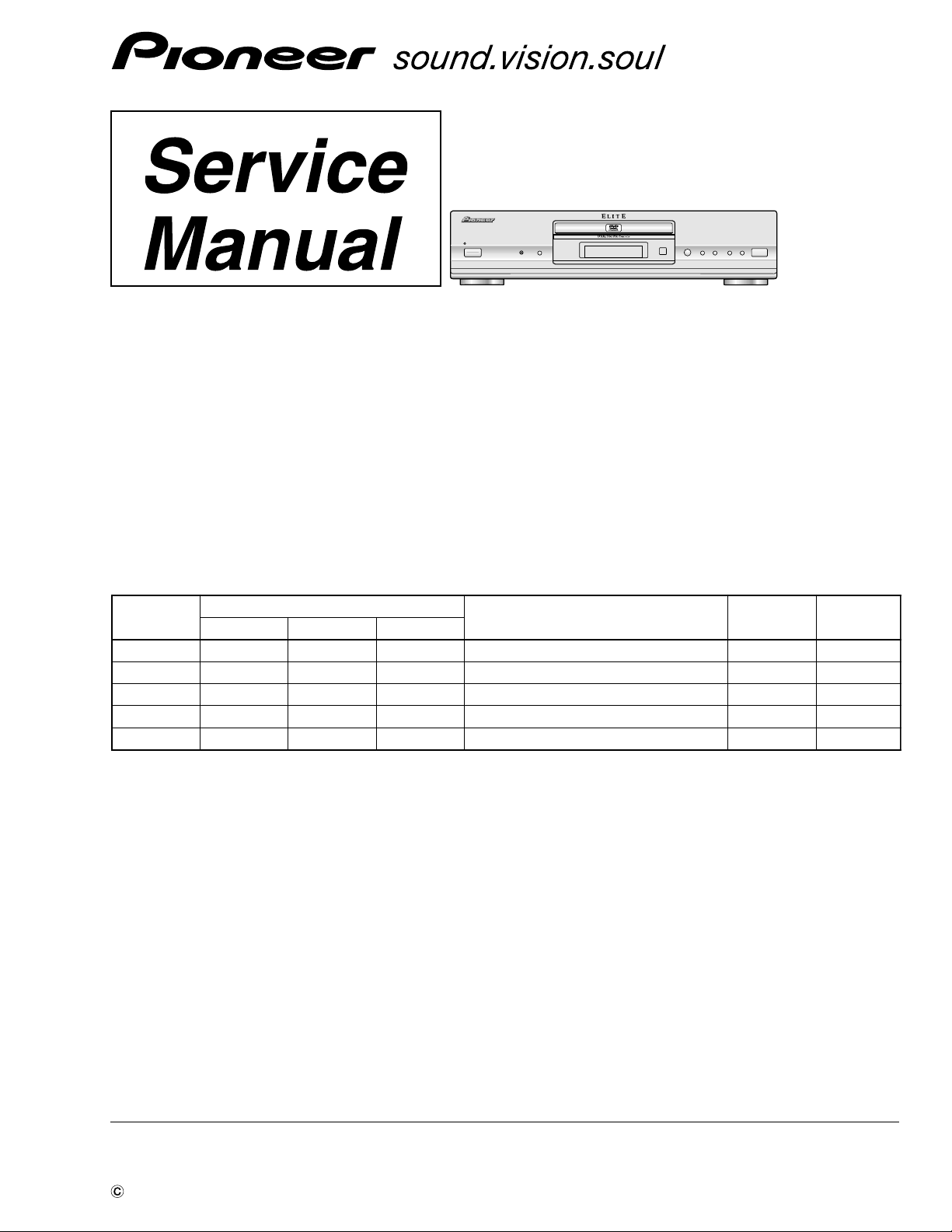
DVD PLAYER
DV-47A
DV-S733A
DV-747A
THIS MANUAL IS APPLICABLE TO THE FOLLOWING MODEL(S) AND TYPE(S).
Type
KUXJ/CA ? −−AC120V 1
LBXJ − ? − AC110V 3
WLXJ/NC − ? − AC220-240V 3
WLXJ/RD − ? − AC220-240V 4
WYXJ −−? AC220-240V 2
DV-47A DV-S733A DV-747A
Model
Power Requirement Region No. Remarks
ORDER NO.
RRV2564
CONTENTS
1. SAFETY INFORMATION
2. EXPLODED VIEWS AND PARTS LIST
3. BLOCK DIAGRAM AND SCHEMATIC DIAGRAM
4. PCB CONNECTION DIAGRAM
5. PCB PARTS LIST
6. ADJUSTMENT
PIONEER CORPORATION 4-1, Meguro 1-chome, Meguro-ku, Tokyo 153-8654, Japan
PIONEER ELECTRONICS (USA) INC. P.O. Box 1760, Long Beach, CA 90801-1760, U.S.A.
PIONEER EUROPE NV Haven 1087, Keetberglaan 1, 9120 Melsele, Belgium
PIONEER ELECTRONICS ASIACENTRE PTE. LTD. 253 Alexandra Road, #04-01, Singapore 159936
PIONEER CORPORATION 2001
................................................
.....................................................
.......................................
.................
...
...........................
14
47
60
70
2
4
7. GENERAL INFORMATION
7.1 DIAGNOSIS
7.1.1 ID NUMBER AND ID DATA SETTING.76
7.1.2 SELF-DIAGNOSTIC FUNCTION OF
PICKUP DEFECTIVE
7.1.3 TEST POINTS LOCATION
7.1.4 TEST MODE SCREEN DISPLAY
7.1.5 TROUBLE SHOOTING
7.1.6 ERROR CODE
7.1.7 DISASSEMBLY
7.2 IC
8. PANEL FACILITIES AND SPECIFICATIONS..126
..................................................................
..................................................
................................
...........................
...................
........................
.....................................
....................................
T – ZZE NOV. 2001 Printed in Japan
........
76
76
78
79
81
85
86
90
95
Page 2
DV-47A, DV-S733A, DV-747A
1. SAFETY INFORMATION
This service manual is intended for qualified service technicians ; it is not meant for the casual do-ityourselfer. Qualified technicians have the necessary test equipment and tools, and have been trained
to properly and safely repair complex products such as those covered by this manual.
Improperly performed repairs can adversely affect the safety and reliability of the product and may
void the warranty. If you are not qualified to perform the repair of this product properly and safely, you
should not risk trying to do so and refer the repair to a qualified service technician.
WARNING
This product contains lead in solder and certain electrical parts contain chemicals which are known to the state of California to cause
cancer, birth defects or other reproductive harm.
Health & Safety Code Section 25249.6 – Proposition 65
NOTICE
(FOR CANADIAN MODEL ONLY)
Fuse symbols (fast operating fuse) and/or (slow operating fuse) on PCB indicate that replacement parts must
be of identical designation.
REMARQUE
(POUR MODÈLE CANADIEN SEULEMENT)
Les symboles de fusible (fusible de type rapide) et/ou (fusible de type lent) sur CCI indiquent que les pièces
de remplacement doivent avoir la même désignation.
(FOR USA MODEL ONLY)
1. SAFETY PRECAUTIONS
The following check should be performed for the
continued protection of the customer and service
technician.
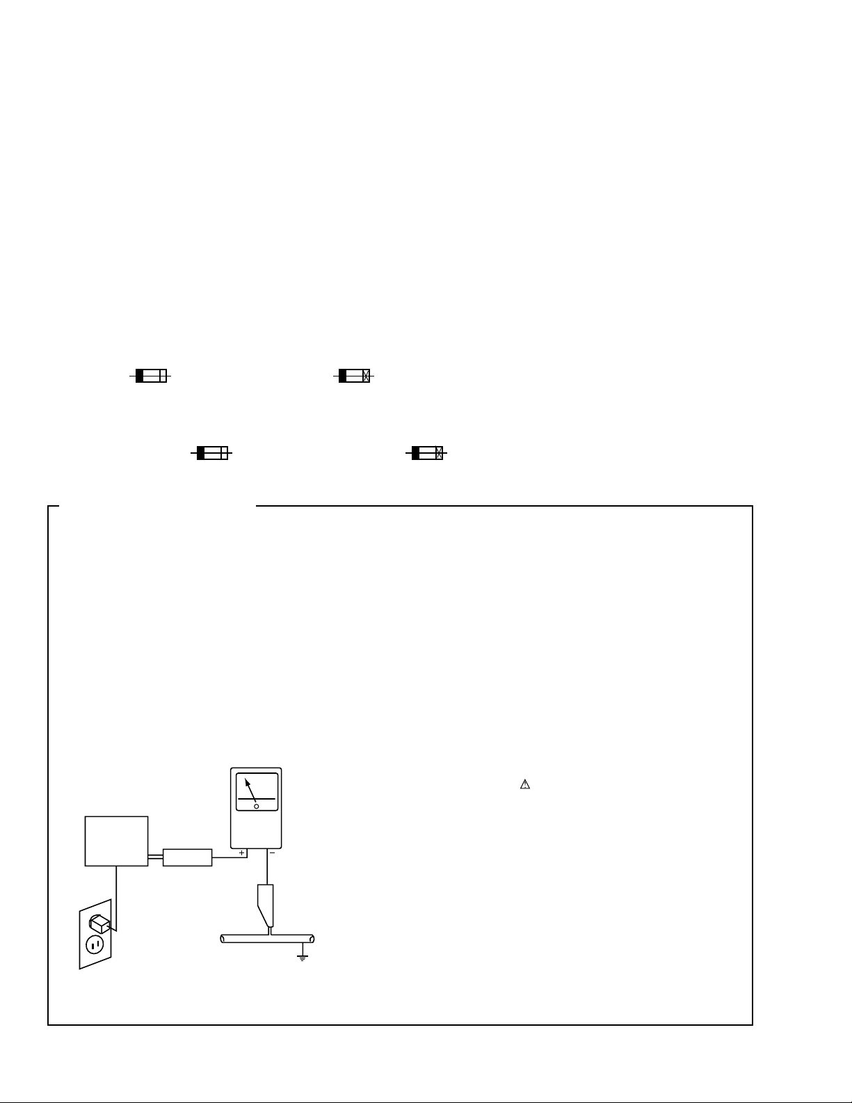
LEAKAGE CURRENT CHECK
Measure leakage current to a known earth ground (water
pipe, conduit, etc.) by connecting a leakage current tester
such as Simpson Model 229-2 or equivalent between the
earth ground and all exposed metal parts of the appliance
(input/output terminals, screwheads, metal overlays, control
shaft, etc.). Plug the AC line cord of the appliance directly
into a 120V AC 60Hz outlet and turn the AC power switch
on. Any current measured must not exceed 0.5mA.
Reading should
not be above
0.5mA
Earth
ground
Device
under
test
Also test with
plug reversed
(Using AC adapter
plug as required)
Leakage
current
tester
Test all
exposed metal
surfaces
ANY MEASUREMENTS NOT WITHIN THE LIMITS
OUTLINED ABOVE ARE INDICATIVE OF A POTENTIAL
SHOCK HAZARD AND MUST BE CORRECTED BEFORE
RETURNING THE APPLIANCE TO THE CUSTOMER.
2. PRODUCT SAFETY NOTICE
Many electrical and mechanical parts in the appliance
have special safety related characteristics. These are
often not evident from visual inspection nor the protection
afforded by them necessarily can be obtained by using
replacement components rated for voltage, wattage, etc.
Replacement parts which have these special safety
characteristics are identified in this Service Manual.
Electrical components having such features are identified
by marking with a
in this Service Manual.
The use of a substitute replacement component which does
not have the same safety characteristics as the PIONEER
recommended replacement one, shown in the parts list in
this Service Manual, may create shock, fire, or other hazards.
Product Safety is continuously under review and new
instructions are issued from time to time. For the latest
information, always consult the current PIONEER Service
Manual. A subscription to, or additional copies of, PIONEER
Service Manual may be obtained at a nominal charge from
PIONEER.
on the schematics and on the parts list
AC Leakage Test
2
Page 3
DV-47A, DV-S733A, DV-747A
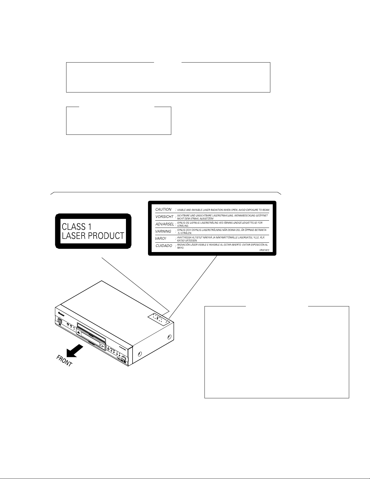
THE AEL (ACCESSIBLE EMISSION LEVEL) OF THE LASER POWER OUTPUT IS LESS THAN CLASS 1
BUT THE LASER COMPONENT IS CAPABLE OF EMITTING RADIATION EXCEEDING THE LIMIT FOR
CLASS 1.
A SPECIALLY INSTRUCTED PERSON SHOULD DO SERVICING OPERATION OF THE APPARATUS.
LASER DIODE CHARACTERISTICS
FOR DVD : MAXIMUM OUTPUT POWER : 5 mW
WAVELENGTH : 655 nm
FOR CD : MAXIMUM OUTPUT POWER : 5 mW
WAVELENGTH : 785 nm
LABEL CHECK
WARNING !
WLXJ/NC, WLXJ/RD and WYXJ types
(Printed on the Rear Panel)
Additional Laser Caution
1. Loading-status detection switch (S101 on the LOAB assy) are detected
by the microprocessor (IC601 in the DVDM assy).
• To permit the laser diode to oscillate, it is required to set the loadingstatus detection switch for the clamp position (the center terminal of S101
is shorted to +3V).
When the voltage of IC101-pin 20 is +3V and IC601 (microprocessor) pin 83 is +3V, 650nm laser diode for DVD oscillates in the DVDM Assy.
When the voltage of IC101-pin 20 is +3V and IC601 (microprocessor) pin 83 is 0V (GND), 780nm laser diode for CD oscillates in the DVDM
Assy.
In the test mode ∗ , the laser diode oscillates when microprocessor detects
a PLAY signal, or when the PLAY key is pressed (S252 ON in the KEYB
assy), with the above requirements satisfied.
2. When the cover is open, close viewing through the objective lens with
the naked eye will cause exposure to the laser beam.
∗ : See page 72.
3
Page 4
DV-47A, DV-S733A, DV-747A
2. EXPLODED VIEWS AND PARTS LIST
NOTES:• Parts marked by "NSP" are generally unavailable because they are not in our Master Spare Parts List.
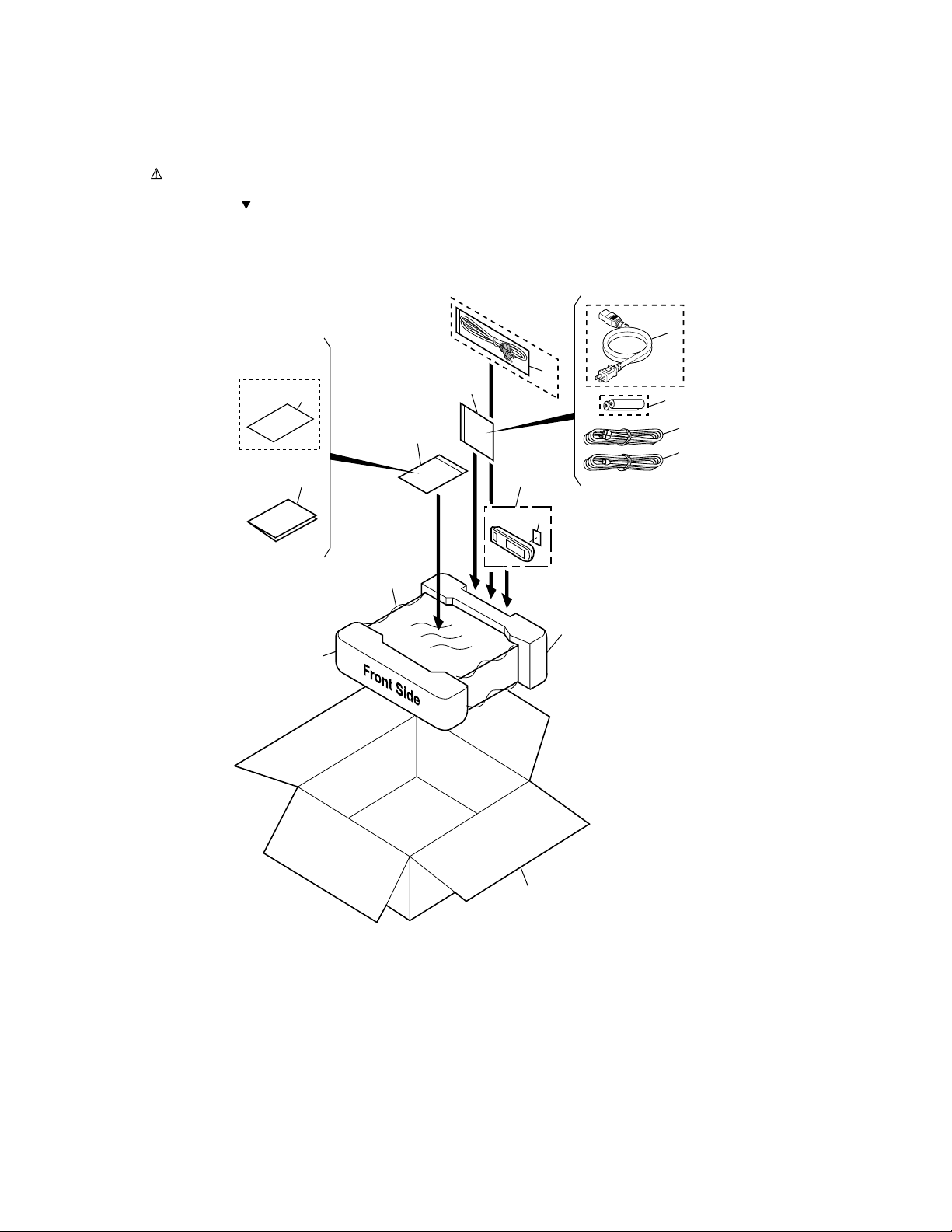
2.1 PACKING
The mark found on some component parts indicates the importance of the safety factor of the part.
•
Therefore, when replacing, be sure to use parts of identical designation.
Screws adjacent to mark on the product are used for disassembly.
•
KUXJ/CA and WYXJ
Types Only
11
13–16
"Operating Instructions"
Except
KUXJ/CA Type
12
17
4
5
10
7
KUXJ/CA Type Only
1
1
6
2
3
8
9
4
Page 5
(1) PACKING PARTS LIST
Mark No. Description Part No.
1 Power Cord See Contrast table (2)
2 Audio Cable (L = 1.5m) VDE1052
3 Video Cable (L = 1.5m) VDE1053
4 Remote Control Unit See Contrast table (2)
5 Battery Cover See Contrast table (2)
NSP 6 Dry Cell Battery (R6P, AA) VEM-013
7 Pad F VHA1288
8 Pad R VHA1289
9 Packing Case See Contrast table (2)
10 Mirror Mat Sheet Z23-007
NSP 11 Warranty Card See Contrast table (2)
12 Polyethylene Bag VHL1051
13 Operating Instructions See Contrast table (2)
(English)
14 Operating Instructions See Contrast table (2)
(Trad-Chinese)
15 Operating Instructions See Contrast table (2)
(English/French/German/Italian)
DV-47A, DV-S733A, DV-747A
16 Operating Instructions See Contrast table (2)
(Spanish/Portuguese/Dutch/Swedish)
17 Polyethylene Bag See Contrast table (2)
(2) CONTRAST TABLE
DV-47A/KUXJ/CA, DV-S733A/LBXJ, WLXJ/NC, WLXJ/RD and DV-747A/WYXJ are constructed the same except for the following :
Part No.
Mark No. Symbol and Description
1
Power Cord
4
Remote Control Unit
5
Battery Cover
9
NSP
NSP
Packing Case
11
Warranty Card
13
Operating Instructions (English)
14
Operating Instructions (Trad-Chinese)
15
Operating Instructions
(English/French/German/Italian)
16
Operating Instructions
(Spanish/Portuguse/Dutch/Swedish)
17
Polyethylene Bag
17
Polyethylene Bag
DV-47A
/KUXJ/CA
ADG7061
VXX2714
VNK4423
VHG2142
ARY7007
VRB1278
Not used
Not used
Not used
Z21-038
Not used
DV-S733A
/LBXJ
ADG7060
VXX2713
VNK4422
VHG2138
Not used
VRB1278
VRC1145
Not used
Not used
Not used
VHL1051
DV-S733A
/WLXJ/NC
ADG1154
VXX2713
VNK4422
VHG2139
Not used
VRB1278
VRC1145
Not used
Not used
Not used
VHL1051
DV-S733A
/WLXJ/RD
ADG1154
VXX2713
VNK4422
VHG2140
Not used
VRB1278
Not used
Not used
Not used
Not used
VHL1051
DV-747A
/WYXJ
ADG7062
VXX2785
VNK4936
VHG2141
ARY7022
Not used
Not used
VRE1096
VRF1059
AHG7032
Not used
Remarks
5
Page 6
DV-47A, DV-S733A, DV-747A
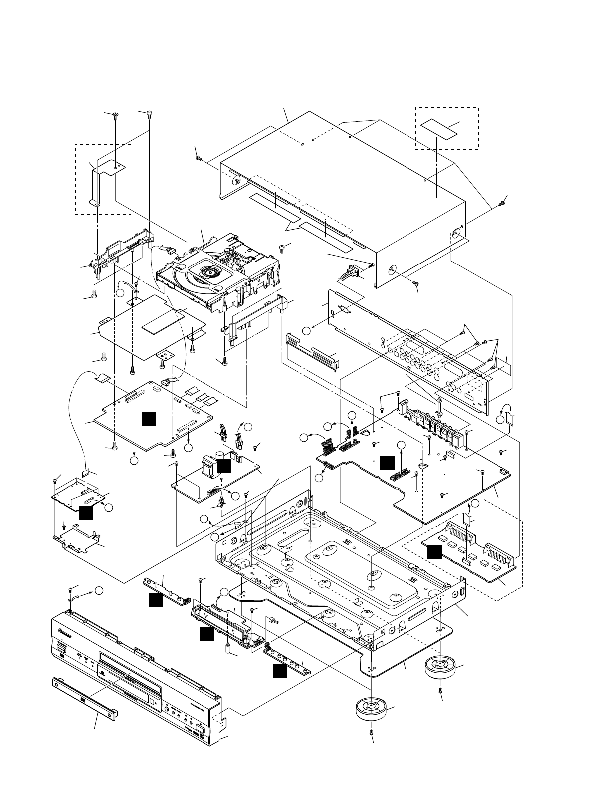
2.2 EXTERIOR SECTION
49
KUXJ/CA
Type Only
50
31
32
34
WLXJ/NC, WLXJ/RD,
WYXJ Types Only
27
29
47
17
33
38
5
33
J
33
41
Refer to
"2.5 LOADING
MECHANISM ASSY".
10
29
H
37
33
33
33
33
7
B
36
29
B
H
C
12
H
33
A
40
G
43
31
30
Except
WLXJ/NC,
WLXJ/RD
Types
18
16
F
F
29
Except
KUXJ/CA
Type
39
9
29
C
G
D
35
42
WYXJ Type Only
29
A
29
C
14
32
30
29
B
29
29
29
29
E
48
30
28
E
29
29
4
8
48
Refer to
"2.4 DOOR SECTION".
6
I
46
3
I
F
29
D
1
29
44
D
WYXJ Type
15
6
Only
E
G
2
45
19
30
19
30
11
Refer to
"2.3 FRONT PANEL SECTION".
Page 7
(1) EXTERIOR PARTS LIST
DV-47A, DV-S733A, DV-747A
Mark No. Description Part No.
1 FLIR Assy See Contrast table (2)
NSP 2 KEYB Assy VWG2306
NSP 3 PWSB Assy See Contrast table (2)
4 AVJB Assy See Contrast table (2)
5 DVDM Assy VWS1471
6 SCRB Assy See Contrast table (2)
7 Connector Assy PG05KK-E15
8 FFC See Contrast table (2)
9 POWER SUPPLY Unit VWR1346
NSP 10 Loading Mechanism Assy VWT1188
11 PCB Support VEC1266
12 PCB Support VEC2184
13 • • • • •
14 PCB Holder See Contrast table (2)
NSP 15 Chassis VNA2160
16 Rear Panel See Contrast table (2)
17 Adapter27 L VNL1926
18 Adapter27 R VNL1927
19 Insulator VXA2424
20 • • • • •
21 • • • • •
22 • • • • •
23 • • • • •
24 • • • • •
25 • • • • •
Mark No. Description Part No.
26 • • • • •
27 Label See Contrast table (2)
NSP 28 ID Label VRW1877
29 Screw BBZ30P060FMC
30 Screw BBZ30P080FZK
31 Screw BBZ30P180FMC
32 Screw See Contrast table (2)
33 Screw PPZ30P080FMC
34 Bonnet Case S See Contrast table (2)
35 AC Inlet Assy See Contrast table (2)
36 Housing Assy VKP2269
37 MH Spacer VEC2250
38 Mechanism Holder VNE2266
39 Earth Lead Unit See Contrast table (2)
NSP 40 SACD Assy VWG2331
41 Flexible Cable VDA1879
42 Shielding Plate VNF1124
43 Cushion VEB1336
44 Bottom Cushion VEB1337
NSP 45 Bottom Plate VNA2345
46 SACD Stay VNE2258
47 Screw BBZ30P040FZK
48 Screw BBZ30P080FCC
49 Screw Z39-019
50 Shielding Plate See Contrast table (2)
(2) CONTRAST TABLE
DV-47A/KUXJ/CA, DV-S733A/LBXJ, WLXJ/NC, WLXJ/RD and DV-747A/WYXJ are constructed the same except for the following :
Part No.
Mark No. Symbol and Description
1
NSP
NSP
FLIR Assy
3
PWSB Assy
4
AVJB Assy
6
SCRB Assy
8
FFC
14
PCB Holder
16
Rear Panel
27
Label
32
Screw
34
Bonnet Case S
35
AC Inlet Assy
39
Earth Lead Unit
50
Shielding Plate
DV-47A
/KUXJ/CA
VWG2327
VWG2312
VWV1874
Not used
Not used
Not used
VNA2366
Not used
BCZ40P060FZK
VXX2750
ADX7406
Not used
VNF1125
DV-S733A
/LBXJ
VWG2325
VWG2310
VWV1877
Not used
Not used
Not used
VNA2368
Not used
BCZ40P060FNI
VXX2766
ADX7405
VDA1903
Not used
DV-S733A
/WLXJ/NC
VWG2324
VWG2310
VWV1875
Not used
Not used
Not used
VNA2369
VRW1872
BCZ40P060FNI
VXX2766
VKP2268
VDA1903
Not used
DV-S733A
/WLXJ/RD
VWG2324
VWG2310
VWV1875
Not used
Not used
Not used
VNA2370
VRW1872
BCZ40P060FNI
VXX2766
VKP2268
VDA1903
Not used
DV-747A
/WYXJ
VWG2326
VWG2311
VWV1876
VWV1850
VDA1870
VEC2215
VNA2367
VRW1872
BCZ40P060FNI
VXX2790
ADX7405
VDA1903
Not used
Remarks
7
Page 8
DV-47A, DV-S733A, DV-747A
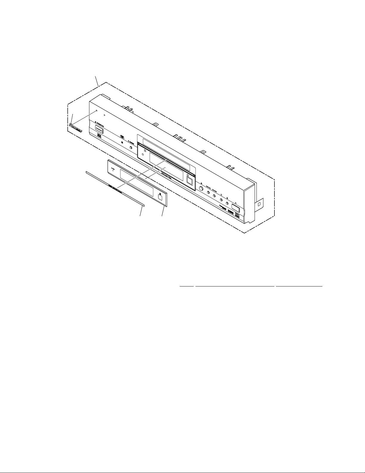
2.3 FRONT PANEL SECTION
7 DV-47A
3
4
1
2
¶ FRONT PANEL PARTS LIST
Mark No. Description Part No.
1 Sub Plate VEC2204
2 FL Lens VEC2230
3 Front Panel Assy VXA2474
4 Pioneer Name Plate VAM1109
8
Page 9
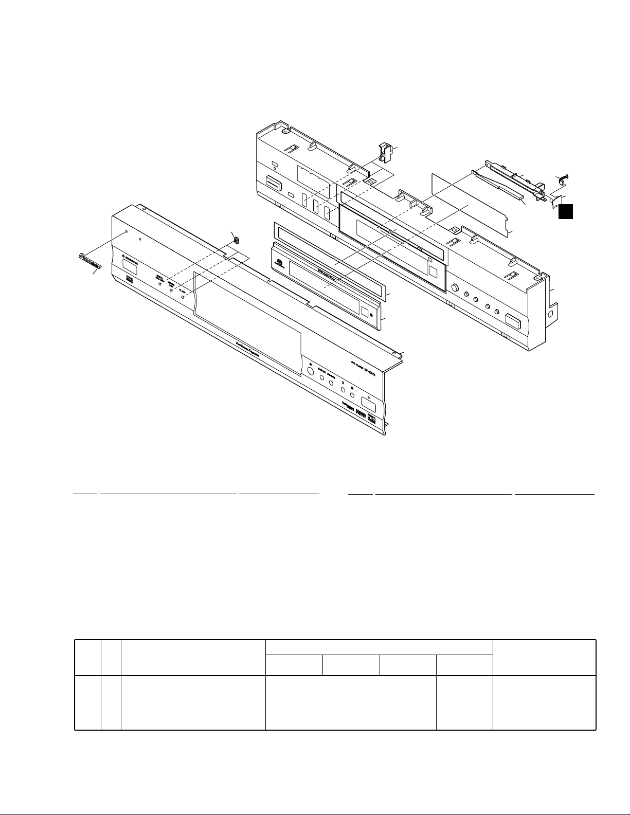
7 DV-S733A, DV-747A
11 (2/2)
DV-47A, DV-S733A, DV-747A
8
10
2
1
9
5
I
3
(1) FRONT PANEL PARTS LIST
Mark No. Description Part No.
NSP 1 DILB Assy VWG2322
2 Connector Assy PF02PP-B20
3 Name Plate See Contrast table (2)
4 AL Panel See Contrast table (2)
5 FL Filter VEC2224
6
7
4
Mark No. Description Part No.
6 Door Cushion See Contrast table (2)
7 FL Lens See Contrast table (2)
8 LED Lens VNK4908
9 Center Lens VNK4910
10 Lens Holder VNK4911
11 (1/2)
11 Panel Base Assy See Contrast table (2)
(2) CONTRAST TABLE
DV-S733A/LBXJ, WLXJ/NC, WLXJ/RD and DV-747A/WYXJ are constructed the same except for the following :
Part No.
Mark No. Symbol and Description
3
Name Plate
4
AL Panel
6
Door Cushion
7
FL Lens
11
Panel Base Assy
DV-S733A
/LBXJ
DV-S733A
/WLXJ/NC
PAN1377
VAH1390
VEC2228
VEC2229
VXA2472
DV-S733A
/WLXJ/RD
DV-747A
/WYXJ
VAM1124
VAH1389
VEC2254
VEC2256
VXA2473
Remarks
9
Page 10
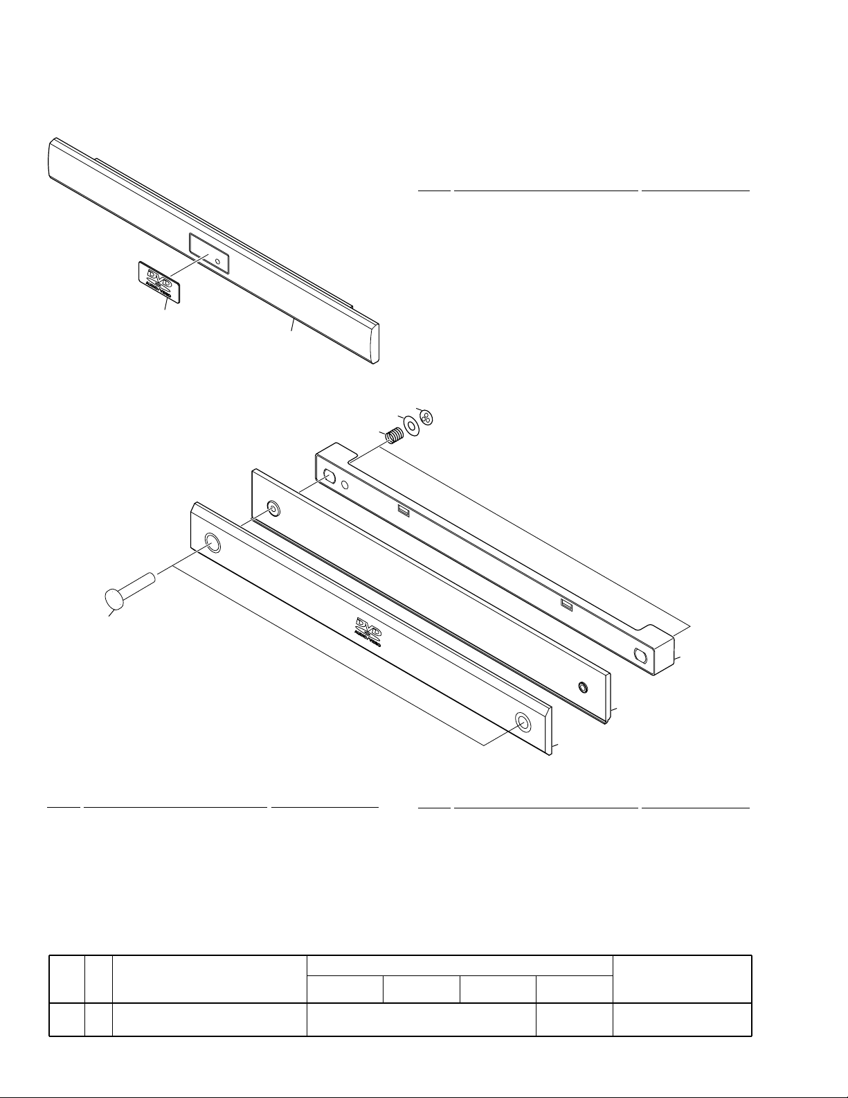
DV-47A, DV-S733A, DV-747A
2.4 DOOR SECTION
7 DV-47A
1
2
7 DV-S733A, DV-747A
¶ DOOR PARTS LIST
Mark No. Description Part No.
1 DVD-A/V Plate VAM1118
2 Tray Panel VNK4819
7
6
2
1
4
3
(1) DOOR PARTS LIST
Mark No. Description Part No.
1 Rivet VBA1083
2 Door Spring VBH1336
3 Door See Contrast table (2)
4 Door Holder See Contrast table (2)
5 Tray Holder VNK4905
Mark No. Description Part No.
6 Washer WC30FMC
7 Retaining Rings YS20FAC
(2) CONTRAST TABLE
DV-S733A/LBXJ, WLXJ/NC, WLXJ/RD and DV-747A/WYXJ are constructed the same except for the following :
Part No.
Mark No. Symbol and Description
34Door
Door Holder
DV-S733A
/LBXJ
DV-S733A
/WLXJ/NC
VEC2227
VNK4904
DV-S733A
/WLXJ/RD
DV-747A
/WYXJ
VEC2255
VNK4942
5
Remarks
10
Page 11
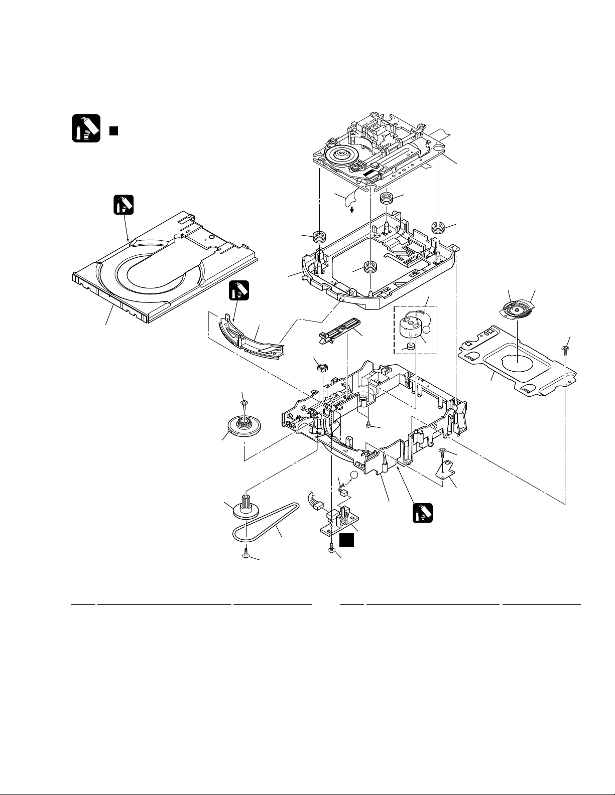
2.5 LOADING MECHANISM ASSY
Note :
Refer to
" Application of Lubricant".
Daifree
GEM1036
DV-47A, DV-S733A, DV-747A
2
Refer to
"2.6 TRAVERSE MECHANISM
6
To DVDM
CN101
8
8
ASSY-S".
8
23
15
14
12
Lubricating Oil
GYA1001
13
22
9
22 22
16
8
20
3
17
21
7
A
11
1
A
A
4
5
22
10
Lubricating Oil
GYA1001
18
22
19
LOADING MECHANISM ASSY PARTS LIST
•
Mark No. Description Part No.
NSP 1 LOAB Assy VWG2279
2 Traverse Mechanism Assy-S VXX2782
3 Loading Motor Assy VXX2505
4 Motor Pulley PNW1634
5 Carriage DC Motor / 0.3W PXM1027
6 Flexible Cable (26P) VDA1864
7 Connector Assy 2P VKP2253
8 Float Rubber VEB1327
9 Belt VEB1330
10 Stabilizer VNE2253
Mark No. Description Part No.
11 Loading Base VNL1917
12 Float Base DVD VNL1918
13 Drive Cam VNL1919
14 Gear Pulley VNL1921
15 Loading Gear VNL1922
16 Drive Gear VNL1923
17 SW Lever VNL1925
18 Clamper Plate VNE2251
19 Bridge VNE2252
20 Clamper VNL1924
21 Screw JGZ17P028FMC
22 Screw Z39-019
23 Tray VNL1920
11
Page 12
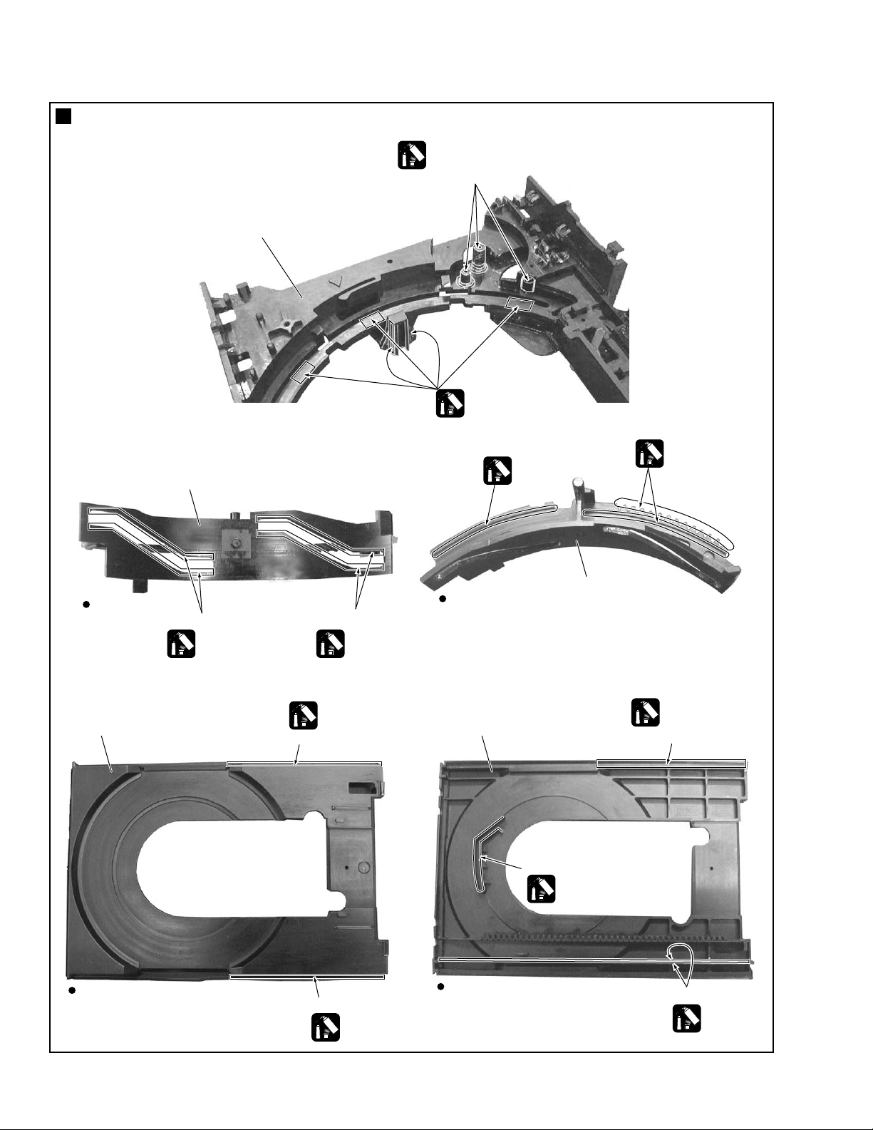
DV-47A, DV-S733A, DV-747A
Application of Lubricant
No. 11
Loading Base
Lubricating Oil
GYA1001
Around the shaft
Lubricating Oil
GYA1001
Rear View
No. 23
Tray
No. 13
Drive Cam
Inner side of a ditch
Lubricating Oil
GYA1001
Inner side of a ditch
Lubricating Oil
GYA1001
Daifree
GEM1036
Concave of unevenness
Top View
No. 23
Tray
Lubricating Oil
GYA1001
Lubricating Oil
GYA1001
No. 13
Drive Cam
Daifree
GEM1036
Concave of unevenness
12
Top View
Concave of unevenness
Daifree
GEM1036
Bottom View
Inner side of a ditch
Daifree
GEM1036
Side of the rib
Daifree
GEM1036
Page 13
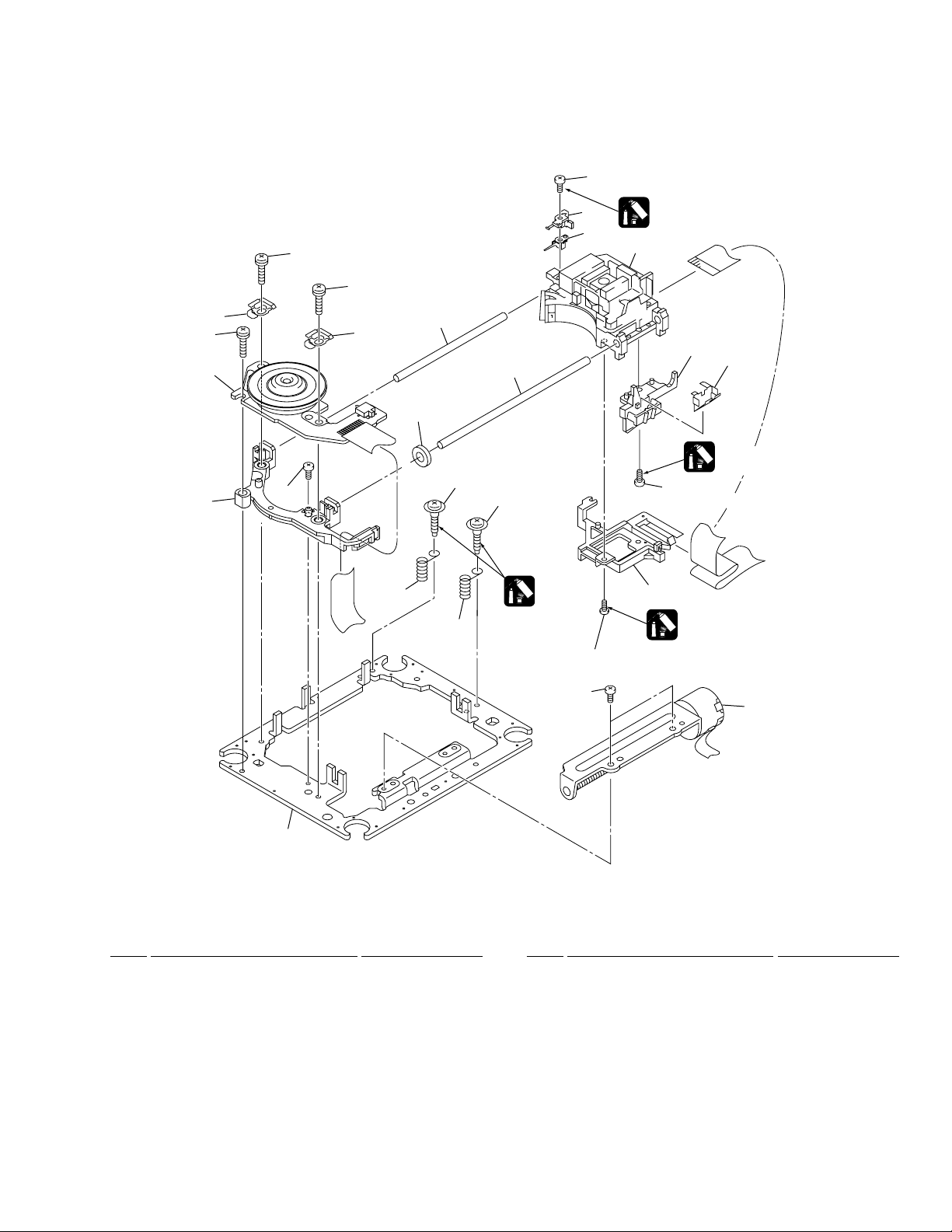
2.6 TRAVERSE MECHANISM ASSY-S
DV-47A, DV-S733A, DV-747A
17 (Torque : 0.12 ± 0.01 N•m)
13
18
10
1
16
18
18
10
12
8
7
6
19
4 (Adjustment Screw)
4 (Adjustment Screw)
5
5
Screw Tight
GYL1001
17 (Torque : 0.12 ± 0.01 N•m)
Silicone Adhesive
GEM1037
3
14
9
Silicone Adhesive
GEM1037
17
(Torque : 0.12 ± 0.01 N•m)
15
Silicone Adhesive
GEM1037
11
TRAVERSE MECHANISM ASSY-S PARTS LIST
•
Mark No. Description Part No.
1 Spindle Motor VXM1088
2 Stepping Motor VXM1090
(CARRIAGE) (or VXM1091)
3 Pickup Assy-S OXX8003
4 Skew Screw VBA1080
5 Skew Spring VBH1335
6 Guide Bar VLL1514
7 Sub Guide Bar VLL1515
8 Hold Spring VNC1017
9 Joint Spring VNC1019
10 Support Spring VNC1020
(or VXM1089)
16
2
Mark No. Description Part No.
NSP 11 Mechanism Chassis VNE2248
12 Slider VNL1811
13 Spacer VNL1913
14 Joint VNL1914
15 FFC Holder VNL1915
16 Screw BBZ20P050FZK
17 Screw OBA8009
18 Screw PMA26P100FMC
19 Damper Sheet VEB1335
13
Page 14
1
23
DV-47A, DV-S733A, DV-747A
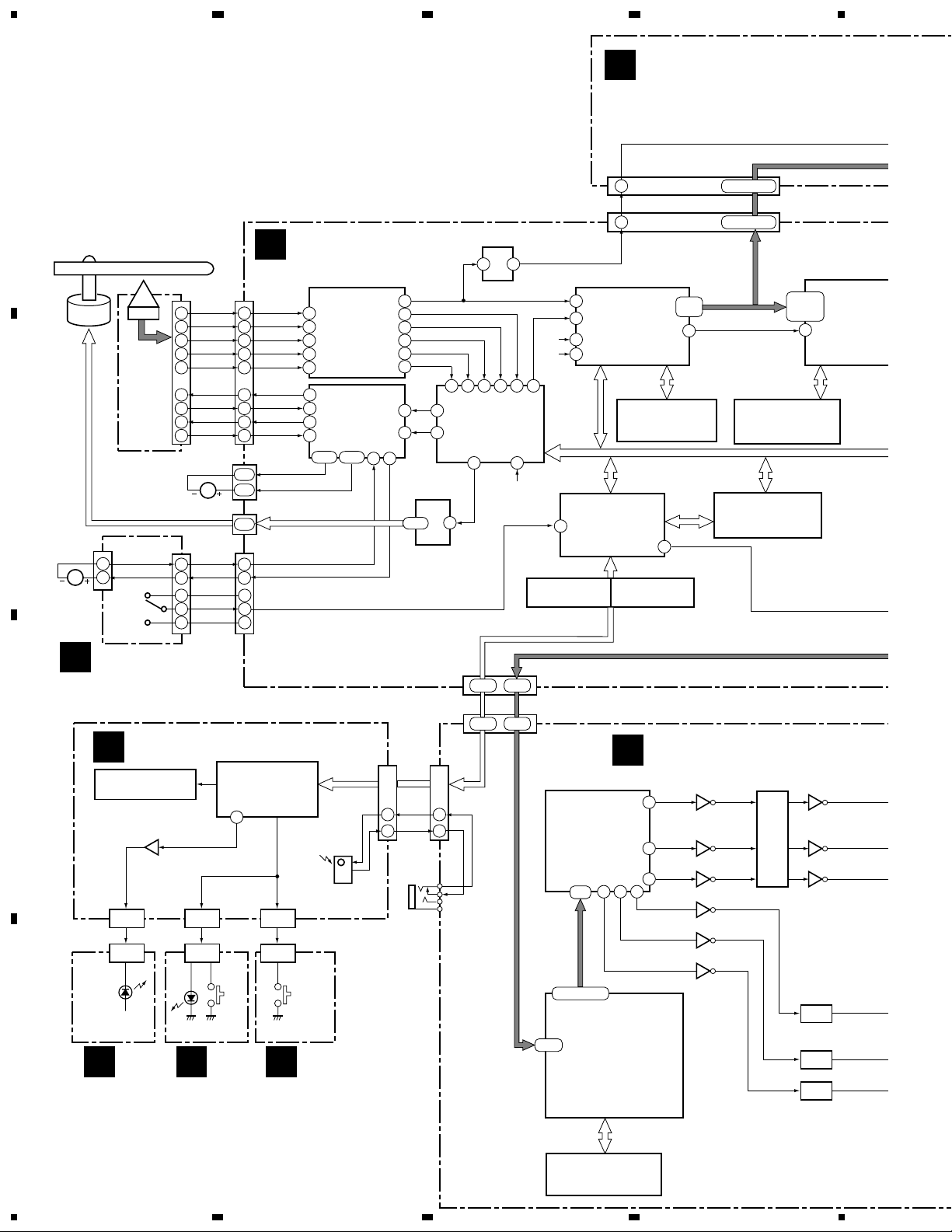
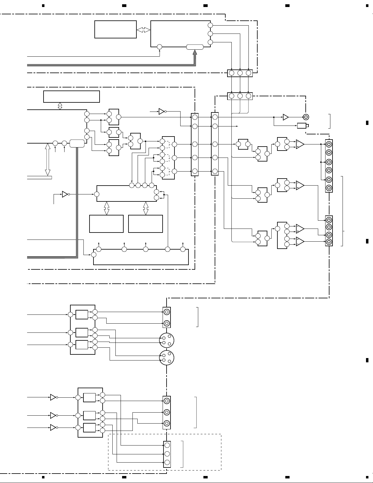
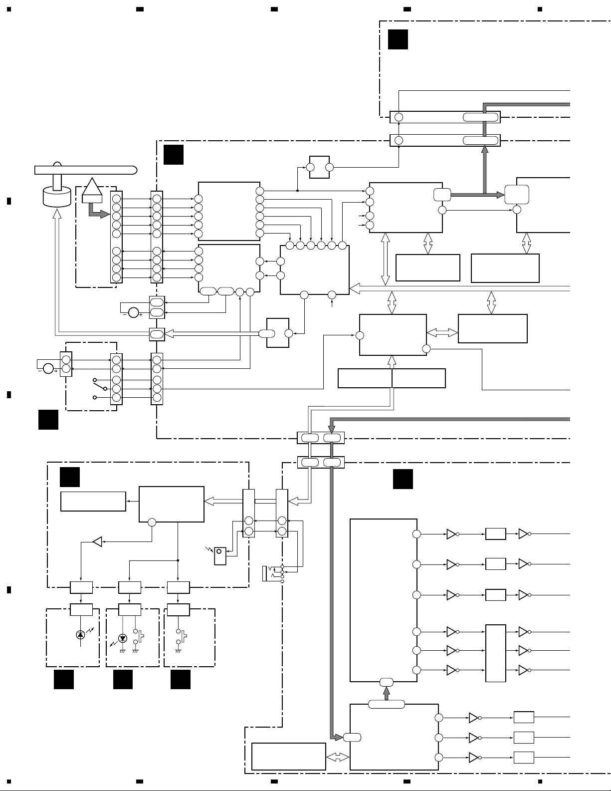
3. BLOCK DIAGRAM
AND SCHEMATIC DIAGRAM
3.1 BLOCK DIAGRAM
A
3.1.1 SIGNAL ROUTE
7 KUXJ/CA, LBXJ, WLXJ/NC and WLXJ/RD Types
DVDM ASSY
B
RF
B1
B2
B3
B4
M
V+3D
SW2
11
20
21
15
16
25
24
23
26
1,2
3,4
4-9
1
2
3
4
5
CN101
(24P)
RF
CN104
CN105
CN103
B1
B2
B3
B4
LOD POS
(12P)
3
IC101
6
LA9701M
7
RF IC
8
9
12
IC351
13
M56788AFP
9
10
DRIVER
34,35
31,32
FTS
15 14
(24P)
Spindle
Motor
PICKUP
ASSY
B
1
2
M
Loading
Motor
S101
Loading
Position
Switch
OEIC
Carriage
Motor
CN601CN602
11
20
21
15
16
25
24
23
26
1
2
3
4
SW1(GNDS)
5
T DRV
T RTN
T DRV
F RTN
LOADLOAD+
RFO
54
DSP RF
46
BH
56
PH
57
FE
42
TE
35
32 33 30 31 39 3
FDO
47
3
TDO
48
20
21
9-14
IC251
BA6664FM
SPDL
DRIVER
IC211
TK15404M
3 2
IC201
LC78652W
SERVO DSP
46 14
SPDO
RFSACD
AIN
ROMXA
33M
16M
16M
LOD POS
3.3V to 5V
CONVERTER
J
24
RFSACD
24
170
IC701
112
PE5220A
DVD DECODER
4
SCRUT
107
GM71VS65803CLT-5
IC601
PD6345A
57
SYSTEM
CONTROL CPU
5V to 3.3V
CONVERTER
SACD ASSY
BD0-BD7
57-60
63-66
CDDATA
111
IC702
64M DRAM
IC603 VYW1896
105
44×48
4
BD0-BD7
CN801 (40P)
CN602 (40P)
149,150,
152-155,
158,159
48
8-12, 35-37
8-12, 35-37
IC802
HY57V161610DTC-8
16M SDRAM
16M FLASH
MEMORY
LOAB ASSY
A
1-10
1-10
FLIR ASSY
C
V101 VAW1085
FL TUBE
Q101
CN102
CN104
(2P)
CN291
(2P)
D
H
DILB
ASSY
(7P)
F
PWSB
ASSY
IC101
PE5251A
FL CONTROL
44
CN103
(4P)
CN201
(7P)
CN251
(4P)
G
KEYB
ASSY
E
CN101
(15P)
REMOTE
SENSOR
IC111
TSOP1840XG1
2
3
SR
IN/OUT
SEL IR
IR
CN403
CN301
(15P)
2
3
16-23
16-23
CN501
(40P)
PD0-PD7
CN601
PD0-PD7
PD0-PD7
27-34
(40P)
IC601
ADV7300KST
12BIT
VIDEO
ENCODER
1-8
9-11, 14-18
IC901
PM0033A
PROGRESSIVE
& HI-QUALITY
VIDEO
ENCODER
AVJB ASSY
C
OUT V AD V
44
OUT C AD C
42
OUT YS AD YS
43
3938 37
OUT Y/G
OUT CR/R
OUT CB/B
VIDEO
Q601 Q701
Q602
Q603
Q604
Q606
Q605
FILTER
Q702
Q703
F721
F723
F722
14
IC902
K4S643232E-TC60
64M SDRAM
1234
Page 15
IC804
M5M4V18165DTP-6S
1MX16 EDO DRAM
IC801
M65774BFP
MPEG2
DECODER
AV-1
95-98,
6455
100-103
27M
36/16M
IC913
TC7SH04FU
24
27MDSP
PD0-PD7
5
IC802
HY57V161610DTC-8
16M SDRAM
IC491
TC74VHC153FT
DOUT0
74
73
71
68
PD0-PD7
4
DOUT1
3
1 23
AO0
1
AO1
2
IC905
TC7WH157FU
IC901 XCA56367PV150
55
DVD AUDIO DSP
IC902
IC61LV6416-12T
1M SRAM
(For IC801,IC913) (For IC201,IC701)
27M
3
14
44×48
CLOCK GENERATOR
WARFI
7
IC904
LC89051V
5
22/24M
IC906
TC74VHC157FT
2
4
3
SDI1
SDO0
SDO1
IC903
IC63LV1024-12T
1M SRAM
16M
36/16M
13
9
IC481 BU2288FV
678
DV-47A, DV-S733A, DV-747A
DSAC
25
18
36
31
33
DOUT
DACCLK
DATA0
DATA1
DATA2
69
76
64
DSARS
DSAL
CN901
(19P)
CN302
(40P)
25
18
36
31
33
5 7 13
DSD_L
DSD_LS
DSD_C
5 7 13
DSD_L
PD0274A
DSD_L
DSD_LS
DSD_C
CN304
(19P)
DSD_LS
DSD_C
DACCLK
IC331
1 24 3
14
13
IC333
TC74VHC157FT
14
13
IC351
TC74VHC157FT
14
13
IC371
TC74VHC157FT
IC441
CS4392D-KS
12
IC501
CS4392D-KS
3
12
IC551
CS4392D-KS
3
12
Q391
19
18
19
18
19
18
15
14
2
1
3
IC442-1/2
NJM5532MD
2
1
3
IC502-1/2
NJM5532MD
IC552-1/2
NJM5532MD
2
1
3
5
7
6
IC552-2/2
NJM5532MD
JA401
COAXIAL
OPTICAL
DIGITAL
AUDIO OUT
JA501
L
R
L
R
L
R
LS
RS
C
LFE
JA502
A
B
5.1CH ANALOG AUDIO 2CH ANALOG AUDIO
IC801
CXD2753R
SACD DECORDER
126
BD0-BD7
IC401
TC7SH04FU
24
10
11
SDO2
65410
TC74VHC157FT
16
28
3
2
5
6
IC908
22/24M
22/24M
10
4
7
9
(For IC701)(For IC801)
CN401
33M
169-176
(40P)
15
IC701 LA7138M
3IN 6OUT VIDEO AMP
V
3
AMP
C
6
AMP
Y
10
AMP
IC702 LA7138M
3IN 6OUT VIDEO AMP
Q706
YIN
10
AMP
Q708
CRIN
6
AMP
Q707
CBIN
3
AMP
5
V
23
V
21
C
19
C
17
Y
15
Y
13
15
13
19
17
23
21
VIDEO OUT
(YELLOW)
VIDEO OUT
JA702
S VIDEO
OUT
JA703
Y (GREEN)
Cb (BLUE)
Cr (RED)
JA704
1
Y
3
Cb
5
Cr
COMPOSITE
COMPONENT
VIDEO OUT
D-CONNECTOR
Except
KUXJ/CA Type
JA701
C
D
15
6
7
8
Page 16
1
23
DV-47A, DV-S733A, DV-747A
7 WYXJ Type
SACD ASSY
J
4
A
24
RFSACD
IC211
DVDM ASSY
B
RF
B1
B2
B3
B4
M
V+3D
SW2
11
20
21
15
16
25
24
23
26
1,2
3,4
4-9
1
2
3
4
5
CN101
(24P)
RF
CN104
CN105
CN103
B1
B2
B3
B4
LOD POS
(12P)
3
IC101
6
LA9701M
7
RF IC
8
9
12
IC351
13
M56788AFP
9
10
DRIVER
34,35
31,32
FTS
15 14
54
DSP RF
46
56
57
42
35
FDO
3
TDO
20
9-14
IC251
BA6664FM
SPDL
DRIVER
(24P)
Spindle
Motor
PICKUP
ASSY
B
OEIC
Carriage
Motor
11
20
21
15
16
T DRV
25
T RTN
24
T DRV
23
F RTN
26
CN601CN602
M
Loading
Motor
1
2
S101
Loading
Position
Switch
1
2
3
4
SW1(GNDS)
5
LOADLOAD+
TK15404M
3 2
RFO
BH
PH
FE
TE
32 33 30 31 39 3
47
IC201
LC78652W
48
SERVO DSP
46 14
SPDO
21
RFSACD
AIN
ROMXA
33M
16M
16M
LOD POS
3.3V to 5V
CONVERTER
57
CONTROL CPU
24
170
IC701
112
PE5220A
DVD DECODER
4
SCRUT
107
GM71VS65803CLT-5
64M DRAM
IC601
PD6345A
SYSTEM
5V to 3.3V
CONVERTER
IC702
105
57-60
63-66
44×48
8-12, 35-37
8-12, 35-37
BD0-BD7
CDDATA
111
IC603 VYW1896
16M FLASH
CN801
(40P)
BD0-BD7
CN602
(40P)
149,150,
152-155,
158,159
48
IC802
HY57V161610DTC-8
16M SDRAM
MEMORY
LOAB ASSY
A
1-10
1-10
FLIR ASSY
E
C
V101 VAW1085
FL TUBE
Q101
CN102
CN104
(2P)
CN291
(2P)
D
H
DILB
ASSY
(7P)
F
PWSB
ASSY
IC101
PE5251A
FL CONTROL
44
CN103
(4P)
CN201
(7P)
CN251
(4P)
G
KEYB
ASSY
CN101
(15P)
REMOTE
SENSOR
IC111
TSOP1840XG1
2
3
SR
IN/OUT
K4S643232E-TC60
16
CN301
SEL IR
2
IR
3
CN403
IC902
64M SDRAM
(15P)
16-23
16-23
CN501
(40P)
PD0-PD7
CN601
PD0-PD7
PD0-PD7
27-34
(40P)
IC601
ADV7300KST
12BIT
VIDEO
ENCODER
1-8
9-11, 14-18
IC901
PM0033A
PROGRESSIVE
& HI-QUALITY
VIDEO
ENCODER
AVJB ASSY
C
OUT CR/R P CR/R
37
OUT Y/G P Y/G
39
OUT CB/B P CB/B
38
OUT V AD V
44
OUT C AD C
42
OUT YS AD YS
43
Q606
Q604
Q605
F708
F706
F707
VIDEO
Q601 Q701
Q602
Q603
P Y PR2 Y
89
P CR PR2 CR
93
P CB PR2 CB
91
FILTER
Q981
Q983
Q982
Q768
Q774
Q771
Q702
Q703
F721
F723
F722
1234
Page 17
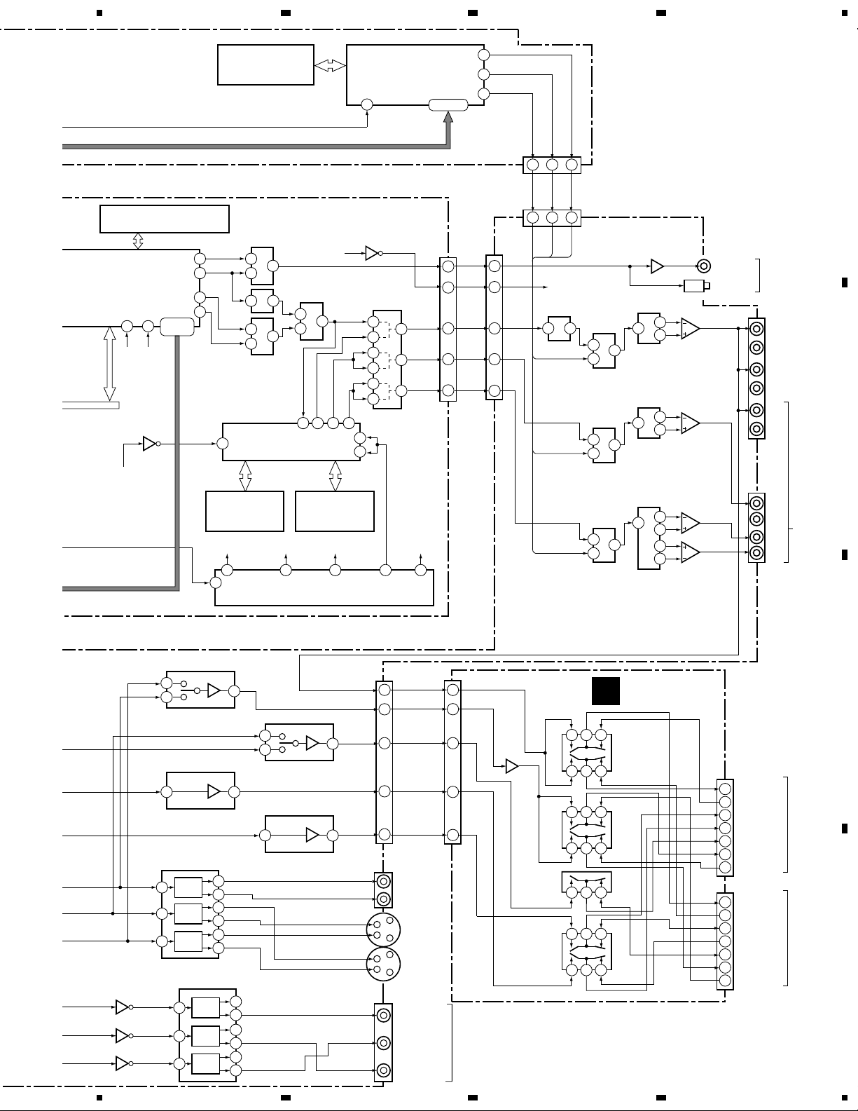
IC804
M5M4V18165DTP-6S
1MX16 EDO DRAM
IC801
M65774BFP
MPEG2
DECODER
AV-1
95-98,
6455
100-103
27M
36/16M
IC913
TC7SH04FU
24
27MDSP
PD0-PD7
5
IC802
HY57V161610DTC-8
16M SDRAM
IC491
TC74VHC153FT
DOUT0
74
73
71
68
PD0-PD7
4
DOUT1
3
1 23
AO0
1
AO1
2
IC905
TC7WH157FU
IC901 XCA56367PV150
55
DVD AUDIO DSP
IC902
IC61LV6416-12T
1M SRAM
(For IC801,IC913) (For IC201,IC701)
27M
3
14
44×48
CLOCK GENERATOR
WARFI
7
IC904
LC89051V
5
22/24M
IC906
TC74VHC157FT
2
4
3
SDI1
SDO0
SDO1
IC903
IC63LV1024-12T
1M SRAM
16M
36/16M
13
9
IC481 BU2288FV
678
DV-47A, DV-S733A, DV-747A
DSAC
25
18
36
31
33
DOUT
DACCLK
DATA0
DATA1
DATA2
69
76
64
DSARS
DSAL
CN901
(19P)
CN302
(40P)
25
18
36
31
33
5 7 13
DSD_L
DSD_LS
DSD_C
5 7 13
DSD_L
PD0274A
DSD_L
DSD_LS
DSD_C
CN304
(19P)
DSD_LS
DSD_C
DACCLK
IC331
1 24 3
14
13
IC333
TC74VHC157FT
14
13
IC351
TC74VHC157FT
14
13
IC371
TC74VHC157FT
IC441
CS4392D-KS
12
IC501
CS4392D-KS
3
12
IC551
CS4392D-KS
3
12
Q391
19
18
19
18
19
18
15
14
2
1
3
IC442-1/2
NJM5532MD
2
1
3
IC502-1/2
NJM5532MD
IC552-1/2
NJM5532MD
2
1
3
5
7
6
IC552-2/2
NJM5532MD
JA401
COAXIAL
OPTICAL
DIGITAL
AUDIO OUT
JA501
L
R
L
R
L
R
LS
RS
C
LFE
JA502
A
B
5.1CH ANALOG AUDIO 2CH ANALOG AUDIO
IC801
CXD2753R
SACD DECORDER
126
BD0-BD7
IC401
TC7SH04FU
24
10
11
SDO2
65410
TC74VHC157FT
16
28
3
2
5
6
IC908
22/24M
22/24M
10
4
7
9
(For IC701)(For IC801)
CN401
33M
169-176
(40P)
15
Y
6
V
4
IC710 MM1508XN
6dB 75Ω DRIVER
G
4
IC707 MM1509XN
6dB 75Ω DRIVER
IC701 LA7138M
3IN 6OUT VIDEO AMP
V
3
AMP
C
6
AMP
Y
10
AMP
IC702 LA7138M
3IN 6OUT VIDEO AMP
Q706
YIN
10
AMP
Q708
CRIN
6
AMP
Q707
CBIN
3
AMP
5
2
C
R
IC708 MM1506XN
6dB 75Ω DRIVER
2
B
IC706 MM1509XN
V
23
V
21
C
19
C
17
Y
15
Y
13
15
13
19
17
23
21
6
4
4
2
2
6dB 75Ω DRIVER
CN702
(16P)
AUDIOL
2
10
16
14
12
JA701
COMPOSITE
VIDEO OUT
(YELLOW)
JA702
S VIDEO
OUT
JA703
Y (GREEN)
Cb (BLUE)
Cr (RED)
6
R/C
Y/V
G
B
CN101
(16P)
15
7
1
3
5
COMPONENT
VIDEO OUT
Q311
4 3 2
7 8 9
4 3 2
7 8 9
7 8 9
4 3 2
7 8 9
7
SCRB ASSY
D
RY101
RY301
RY201
RY203
EURO
CONNECTOR
JA101
(21P)
AUD. L OUT
3
AUD. L IN
6
B OUT
7
G OUT
11
R/C OUT
15
V/Y OUT
19
V/Y IN
20
JA102
(21P)
AUD. L OUT
3
AUD. L IN
6
B IN (C OUT)
7
G IN
11
R/C IN (C OUT)
15
V/Y OUT
19
V/Y IN
20
8
C
OUT
IN
D
17
Page 18
1
23
DV-47A, DV-S733A, DV-747A
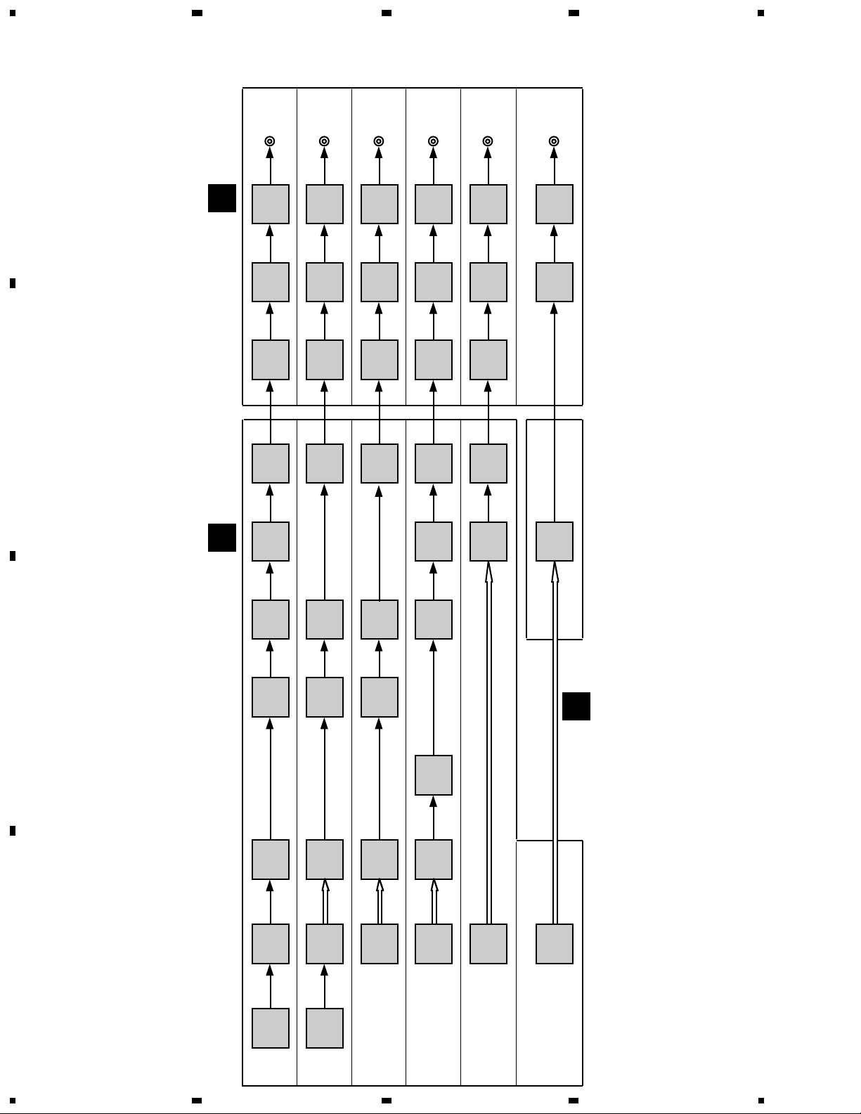
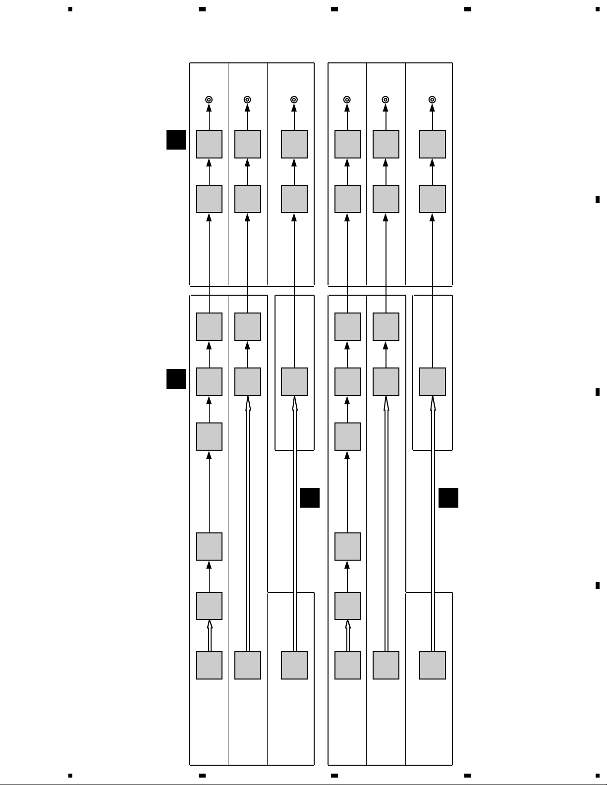
3.1.2 AUDIO DATA STREAM (ANALOG OUTPUT)
4
JA501
JA501
JA501
JA501
JA501
JA501
A
DAC
IC441
IC333
TC74VHC
18,19
14,15,
CS4392
3, 4
9,1257–66
157FT
10, 13
AVJB ASSY
C
DAC
IC441
IC333
TC74VHC
AQE
IC331
18,19
CS4392
3
157FT14 12
24 14,15,
PD0274A
1
DAC
IC441
IC333
TC74VHC
AQE
IC331
18,19
14,15,
CS4392
3
157FT14 12
24
PD0274A
1
DAC
IC441
IC333
TC74VHC
AQE
IC331
18,19
14,15,
CS4392
3
157FT14 12
24
PD0274A
1
DAC
IC441
IC333
TC74VHC
AQE
IC331
18,19
14,15,
CS4392
3
157FT14 12
24
PD0274A
1
DAC
IC441
IC333
TC74VHC
AQE
IC331
18,19
14,15,
CS4392
3
157FT14 12
24
PD0274A
1
B
IC908
157FT 4
TC74VHC
2
DVDM ASSY
IC908
TC74VHC
4149–
157FT 4
IC908
157FT
TC74VHC
3
3
IC908
TC74VHC
4149–
157FT
2
IC908
TC74VHC
157FT
42 4
64, 66
DSP
B
IC901
XCA56367
410 4
157FT
TC74VHC
3
5
C
IC905
AOD IC906
IC801
CDDATA
IC701
AV1
157FU
TC7WH
68 2
M65774BFP
48
111
SCRUT
PE5220A
IC905
AOD IC906
IC801
BD0–7
IC701
AV1
4
157FT
TC74VHC
3
5
157FU
TC7WH
68 2
M65774BFP
159
149–
66
57–
SCRUT
PE5220A
IC905
AO0 IC906
IC801
BD0–7IC701
TC74VHC
TC7WH
AV1
SCRUT
4
157FT
3
5
157FU
1
71
M65774BFP
57–
PE5220A
DSP
IC901
XCA56367
10 4
4
IC906
157FT
TC74VHC
2
23
DIR
IC904
LC89051V
1
DOUT1
73
AV1
IC801
M65774BFP
159
BD0–7IC701
66
SCRUT
PE5220A
57–
DSP
IC901
XCA56367
34–43
IC801
CXD2753R
169–176
SACD
ASSY
J
ASDATA0–7
159
66
IC701
126–135
SCRUT
PE5220A
BD0–7
IC701
SCRUT
PE5220A
D
18
ROMXA
IC201
SERVO DSP
CD
<L/R>
311
LC78652W
ROMXA
IC201
SERVO DSP
VCD
MP3
311
LC78652W
DVD LPCM
DVD AC3 5.1ch
dts
MPEG audio
DVD-A
SACD
1234
Page 19
1
234
DV-47A, DV-S733A, DV-747A
JA502
DAC
IC501
IC351
TC74VHC
IC908
TC74VHC
18,19
14,15,
CS4392
3
157FT 12
14
7149–
157FT
5,6
AVJB ASSY
C
DVDM ASSY
JA502
DAC
IC501
IC351
TC74VHC
IC908
TC74VHC
14,15,18,19
CS4392
3
12
157FT
14
7
157FT
6
55,
JA502
DAC
IC501
IC351
TC74VHC
18,19
14,15,
CS4392
3, 4
9,1257–66
157FT
10, 13
74, 76
JA502
DAC
IC551
IC371
TC74VHC
IC908
TC74VHC
18,19
14,15,
CS4392
3
157FT 12
14
9149–
157FT
10,1
JA502
DAC
IC551
IC371
TC74VHC
IC908
TC74VHC
18,19
14,15,
CS4392
3
12
157FT
14
157FT
6 10,1 9
JA502
DAC
IC551
IC371
TC74VHC
18,19
14,15,
CS4392
3, 4
9,1257–66
157FT
10, 13
69, 71
A
B
B
IC901
IC906
IC904
DOUT1
AV1
IC801
BD0–7IC701
DSP
TC74VHC
DIR
SCRUT
XCA56367
10 5
4
157FT
2
23
LC89051V
1
73
M65774BFP
159
66
57–
PE5220A
IC901
ASDATA0–7
IC701
DSP
SCRUT
XCA56367
34–43
126–135
PE5220A
IC801
BD0–7
IC701
CXD2753R
169–176
SCRUT
PE5220A
SACD
ASSY
J
IC901
IC906
IC904
DOUT1
IC801
BD0–7IC701
AV1
DSP
XCA56367
10 6
4
157FT
TC74VHC
2
23
DIR
LC89051V
1
73
M65774BFP
159
66
57–
SCRUT
PE5220A
IC901
ASDATA0–7
IC701
DSP
XCA56367
34–43
126–135
SCRUT
PE5220A
IC801
BD0–7
IC701
CXD2753R
169–176
SCRUT
PE5220A
SACD
ASSY
J
C
D
DVD AC3 5.1ch
dts
<LS/RS>
1
DVD-A
SACD
2
DVD AC3 5.1ch
dts
<C/LFE>
DVD-A
SACD
3
4
19
Page 20
1
23
DV-47A, DV-S733A, DV-747A
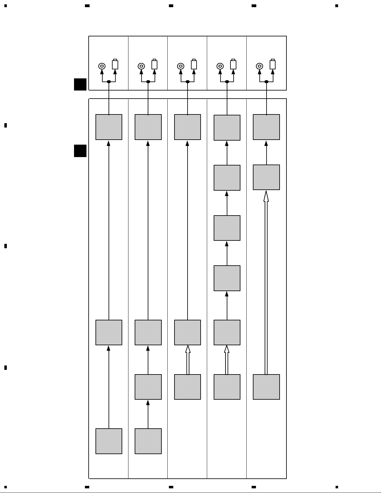
3.1.3 AUDIO DATA STREAM (COAXIAL/OPTICAL OUTPUT)
JA401
JA402
JA401
JA402
JA401
A
AVJB ASSY
C
JA402
JA401
JA402
JA401
4
JA402
IC491
153FT 7
TC74VHC
DVDM ASSY
B
B
DOUT0
IC491
153FT
TC74VHC
47
DOUT0
IC491
TC74VHC
DOUT0
153FT
47149
IC491
153FT
TC74VHC
57
HADO
DSP
IC901
XCA56367
41 2
IC906
157FT
TC74VHC
2
DIR
IC904
LC89051V
12
IC491
153FT
TC74VHC
57
HADO
2
DSP
IC901
XCA56367
43
34–
ASDATA0–7
C
7 4
7
7
DOUT1
7
AV1
IC801
M65774BFP
DOUT
D
14
DSP
IC201
SERVO
LC78652W
CD
AV1
IC801
M65774BFP
4
CDDATA
111
IC701
SCRUT
PE5220A
ROMXA
31
DSP
IC201
SERVO
LC78652W
VCD
MP3
AV1
IC801
M65774BFP
–
159
–
66
BD0–7
57
IC701
SCRUT
PE5220A
MPEG audio
DVD LPCM
DVD AC3
IC801
BD0–7
IC701
dts
AV1
M65774BFP
–
159
149
–
66
57
SCRUT
PE5220A
IC701
DVD-A
126–135
SCRUT
PE5220A
20
1234
Page 21
1
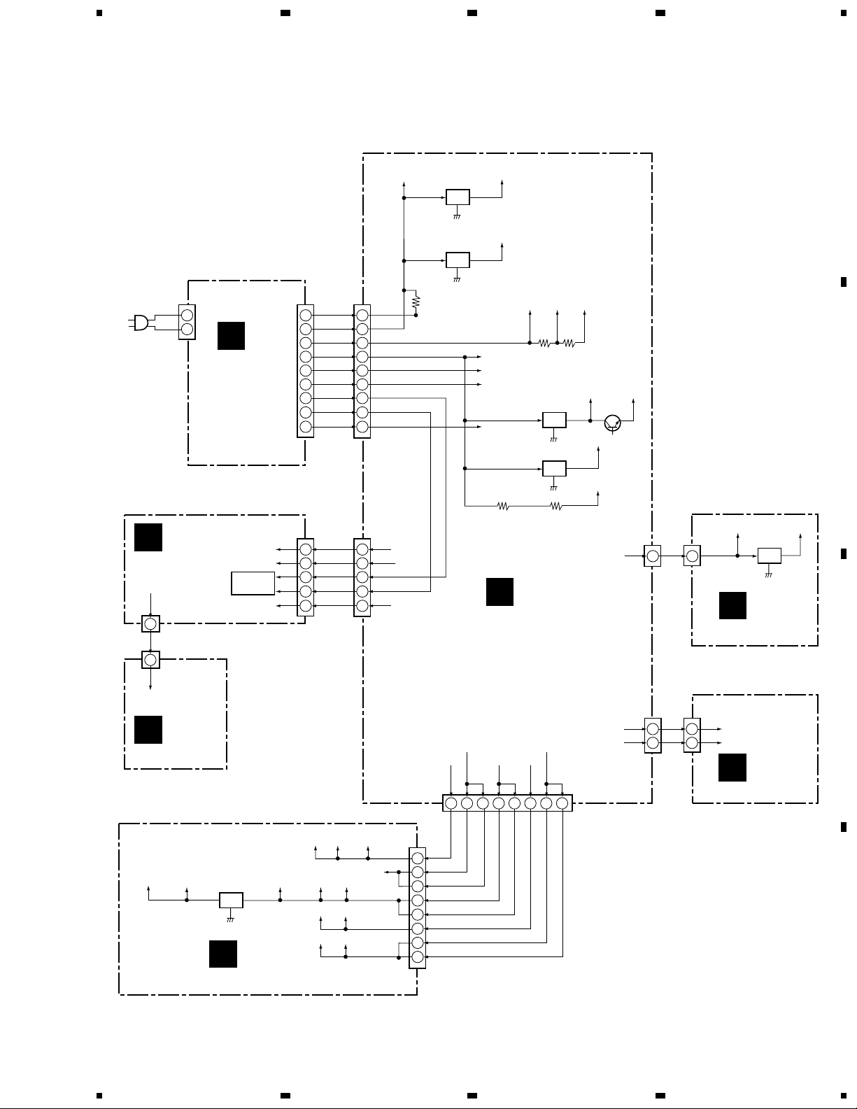
3.1.4 POWER SUPPLY BLOCK
234
DV-47A, DV-S733A, DV-747A
A
V+3V
2.5V REG.
IC921
BA25BCOFP
V+2R5D
AC IN
NEUTRAL
E
FLIR ASSY
V+12V
V+12V
I
DILB ASSY
CN001
LIVE
1
2 2
CN101
H
POWER
SUPPLY
UNIT
CN101
V+12V
V+5E
FL TUBE
CN104
(2P)
1
V+12
1
CN291
(2P)
(14P)
SW+3.3V
1 1
SW+3.3V
2
SW+5V
4 4
SW+12V
6 6
M+6V
8 8
EVER+5V
10 10
12 12
13 13
14 14
(15P)
1 1
EVER+5V
10 10
12 12
13 13
14 14
FLAC
FLAC
-27V
V+12
FLAC
FLAC
-27V
CN303
(14P)
CN301
(15P)
V+12V
V+5E
-27V-27V
2.5V REG.
IC301
BA25BCOFP
R439
V+2R5V
V+12V
V+6M
V+5E
-27V
5V REG.
R800 R793
C
AVJB ASSY
V+5V
V+3V V+12V
2 5 7 8 10 9 12 14
+5V V+5A
V+5V
R794 R790
10V REG.
IC421
PQ15RW11
IC422
NJM78M05FA
V+2R5VV+6M
VREG
V+5A
V+12V
CN302
(40P)
Q421
V+3V
+12V
+5V
V+10A
CN304
(19P)
CN702
(16P)
3.3V
19 19
+12V
+5V
V+3V V+2V
CN901
(19P)
BA25BC0FP
2V REG.
J
SACD ASSY
CN101
(16P)
143
V+12V
125
V+5V
D
SCRB ASSY
B
IC903
C
1.8V REG.
IC909
MM1561JF
B
DVDM ASSY
1
V+5S
CN401
SW+5VV+5D
V+3DV3VDV18DV18_ADSP1 V+3_18REG
V+12V12M
V25VV+2A
V+6M
(40P)
5V
2
6V
5
6V
7
3.3V
8
3.3V
10
12V
9
2.5V
12
2.5V
14
D
21
2
3
4
Page 22
1
23
DV-47A, DV-S733A, DV-747A
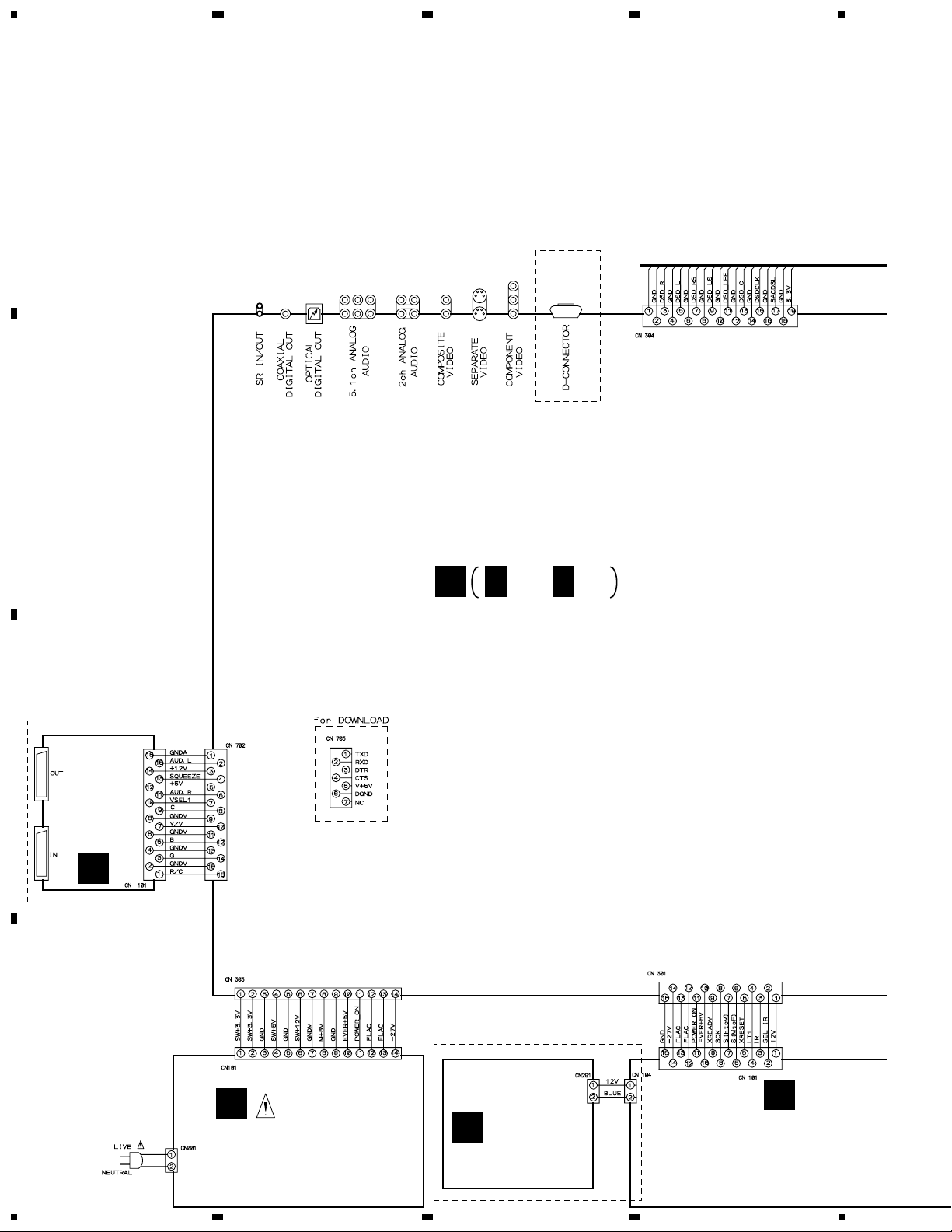
3.2 LOAB ASSY and OVERALL WIRING DIAGRAM
Note : When ordering service parts, be sure to refer to
A
B
"EXPLODED VIEWS and PARTS LIST" or "PCB
PARTS LIST".
4
LBXJ,
WLXJ/NC,
WLXJ/RD
ONLY
33M
WYXJ ONLY
C
D
SCRB ASSY
(VWV1850)
C
AVJB ASSY
(KUXJ/CA : VWV1874)
(LBXJ : VWV1877)
(WLXJ/NC, WLXJ/RD : VWV1875)
(WYXJ : VWV1876)
Except KUXJ/CA
C 1/3- C 3/3
D
E
22
H
POWER SUPPLY UNIT
(VWR1346)
1234
DILB ASSY
I
(VWG2322)
FLIR ASSY
(KUXJ/CA : VWG2327)
(LBXJ : VWG2325)
(WLXJ/NC : VWG2324)
(WLXJ/RD : VWG2324)
(WYXJ : VWG2326)
Page 23
5
33M
678
DV-47A, DV-S733A, DV-747A
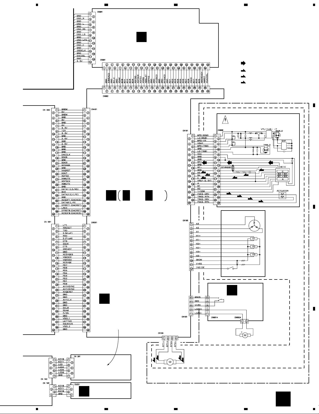
SACD ASSY
J
(VWG2331)
XMSLAT2
B
B 1/4- B 4/4
DVDM ASSY (VWS1471)
(RF)
: RF SIGNAL ROUTE
(F)
: FOCUS SERVO LOOP LINE
(T)
: TRACKING SERVO LOOP LINE
(S)
: SLIDER SERVO LOOP LINE
A
PICKUP ASSY-S (OXX8003)
(RF)(RF)(RF)
(F)
(F)
(T)
(F)
(T)
SPINDLE
MOTOR
: VXX1088
(T)
(T)
(F)
(F)
(F)
B
C
PWSB ASSY
F
(KUXJ/CA : VWG2312)
(LBXJ : VWG2310)
A
LOAB ASSY
(VWG2279)
(WLXJ/NC : VWG2310)
(WLXJ/RD : VWG2310)
(WYXJ : VWG2311)
LOADING
MOTOR
ASSY
: VXX2505
(S)
(S)
KEYB ASSY
G
(VWG2306)
5
6
(S)
STEPPING MOTOR
(S)
(CARRIAGE)
: VXM1090
TRAVERSE MECHANISM
ASSY-S (VXX2782)
LOADING MECHANISM ASSY (VWT1188)
A
7
8
23
D
Page 24
1
23
DV-47A, DV-S733A, DV-747A
4
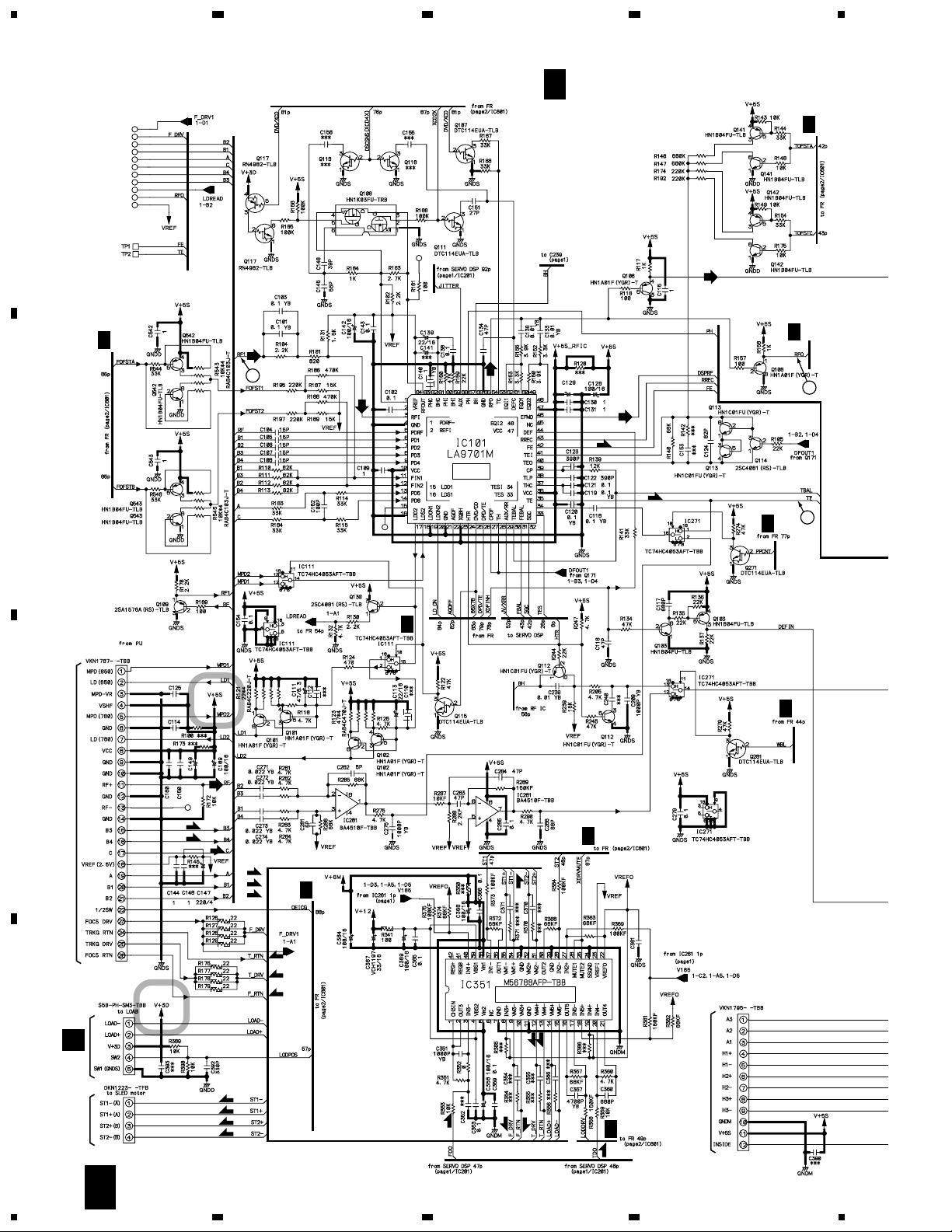
3.3 DVDM ASSY (1/4)
A
B
2/4
B
(RF)
B 1/4
1
(RF)
(V)
RF IC
DVDM ASSY (VWS1471)
(V)
100/6.3
(A)
(F)
(T)
B
2/4
B
3/4
2
4
B
2/4
C
D
PICKUP ASSY
A
CN601
CN101
CN103
B
2/4
1
1
100/6.3
1
1
(RF)
(F)
(F)
(T)
(T)
(F)
(F)
B
2/4
(T)
(T)
(F)
(S)
FTS DRIVER
(T)(T)
B
2/4
1
CN105
B
2/4
MOTOR
CN104
CARRIAGE
24
B
(S)
(S)
(S)
(S)
(F)
(F)
(F)
B
2/4
(T)
SPINDLE
MOTOR ASSY
1/4
1234
Page 25
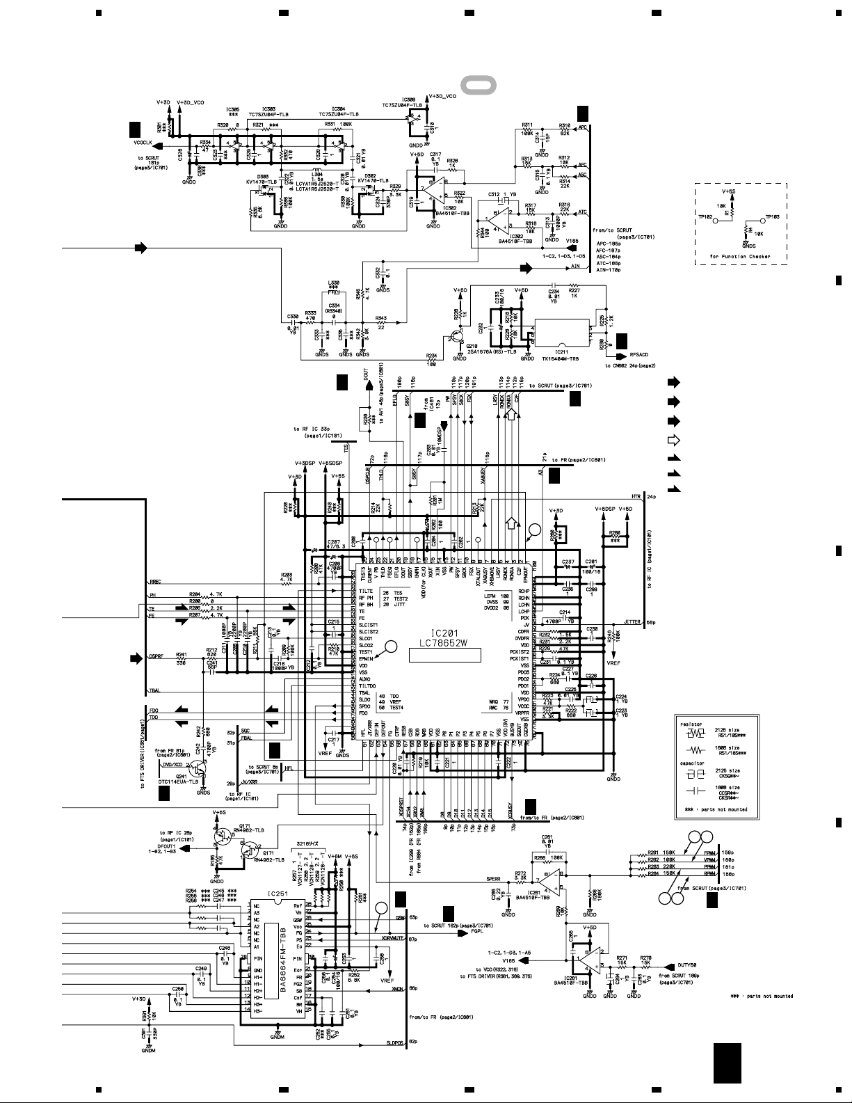
5
678
DV-47A, DV-S733A, DV-747A
: The power supply is shown with the marked box.
B
3/4
B
3/4
220/4
(V)
(V)
B
2/4
(RF)
B
3/4
B
3/4
B
2/4
B
2/4
: RF SIGNAL ROUTE
(V)
: RF (VIDEO) SIGNAL ROUTE
(A)
: RF (AUDIO) SIGNAL ROUTE
(AD)
: AUDIO DATA SIGNAL ROUTE
(F)
: FOCUS SERVO LOOP LINE
(T)
: TRACKING SERVO LOOP LINE
(S)
: SLIDER SERVO LOOP LINE
A
B
C205
VCH1195
150/4
(T)
(F)
(A)
(F)
(T)
B
2/4
(T)
(F)
5
SERVO DSP
(F)
(T)
B
3/4
B
2/4
7
B
3/4
(AD) (AD)
6
220/4
C
B
2/4
8 9
1110
B
3/4
D
SPDL DRV IC
1/4
B
5
6
7
8
25
Page 26
1
23
DV-47A, DV-S733A, DV-747A
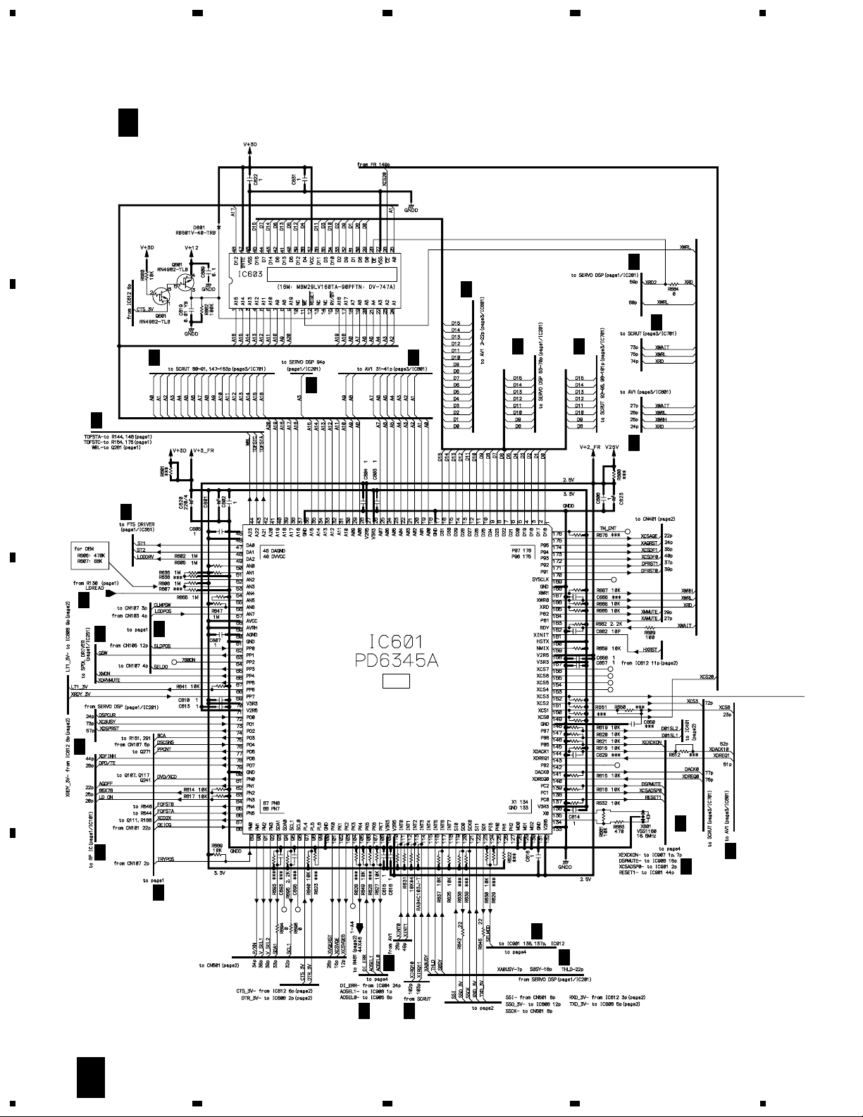
3.4 DVDM ASSY (2/4)
4
B 2/4
A
B
B
1/4
B
1/4
DVDM ASSY (VWS1471)
PGM FLASH MEMORY
VYW1896
B
3/4
VCH1195 150/4
B
1/4
B
3/4
B
3/4
B
B
3/4
B
1/4
1/4
B
3/4
B
3/4
150/4
B
1/4
B
B
1/4
C
B
1/4
B
1/4
D
1/4
FR
B
3/4
B
3/4
B
4/4
B
1/4
B
4/4
B
B
3/4
1/4
26
B
4/4B3/4
2/4
B
1234
Page 27
5
678
DV-47A, DV-S733A, DV-747A
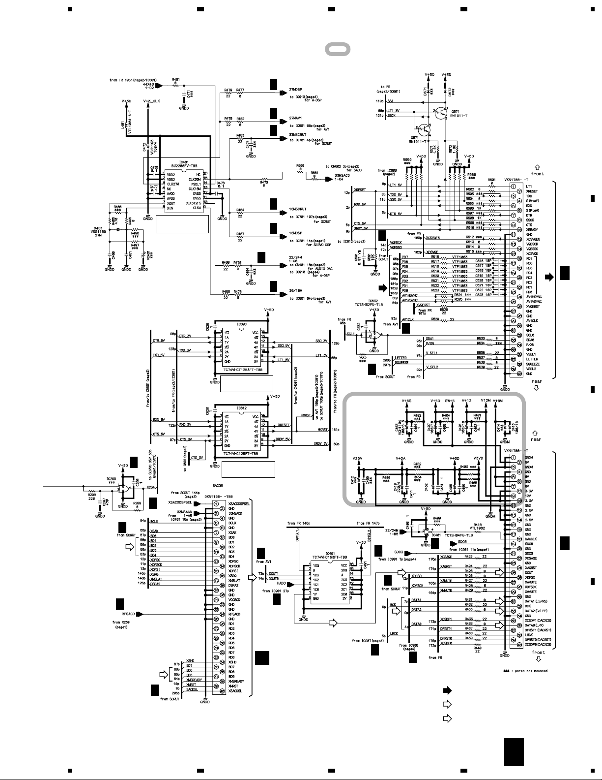
: The power supply is shown with the marked box.
B
4/4
A
B
3/4
B
3/4
CN501
B
3/4
CLOCK
GENERATOR
10P
10P
B
B
2/4, 4/4
B
1/4
3/4
(VD)
B
3/4
(VD)
C 2/3
CN601
B
(AD)
B
B
3/4
B
3/4
3.3→5V
CONVERTOR
CN401
B
1/4
B
3/4
B
3/4
1/4
5→3.3V
CONVERTOR
CN602
(D)
150/4
150/4
B
B
B
3/4
B
4/4
(D)
4/4
B
(D)
3/4
(D)
4/4
CN302
(D)
(D)
(D)
(D)
C
C 1/3
B
J
4/4
(AD)
B
3/4
5
CN801
6
B
4/4
(VD)
: VIDEO DATA SIGNAL ROUTE
(AD)
: AUDIO DATA SIGNAL ROUTE
(D)
: AUDIO (DIGITAL) SIGNAL ROUTE
2/4
B
7
8
27
D
Page 28
1
DV-47A, DV-S733A, DV-747A
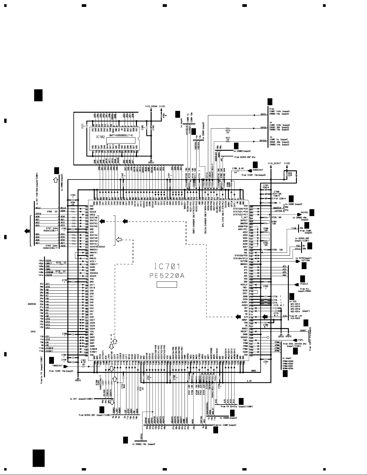
3.5 DVDM ASSY (3/4)
A
23
4
B 3/4
B
(VD)
DVDM ASSY (VWS1471)
64M DRAM
B
2/4
(AD)
(VD) (V)
(AD)
150/4
B
2/4, 4/4
B
4/4
B
2/4
B
2/4
B
2/4
C219
220/4
B
2/4
B
2/4
B
4/4
B
1/4
B
1/4
B
B
1/4
1/4
B
1/4
1/4
B
2/4
SCRUT
C
(V) (V)
(AD)
B
2/4
B
(AD)
B
2/4
B
D
1/4
B
2/4
B
4/4
B
2/4
28
3/4
B
1234
Page 29
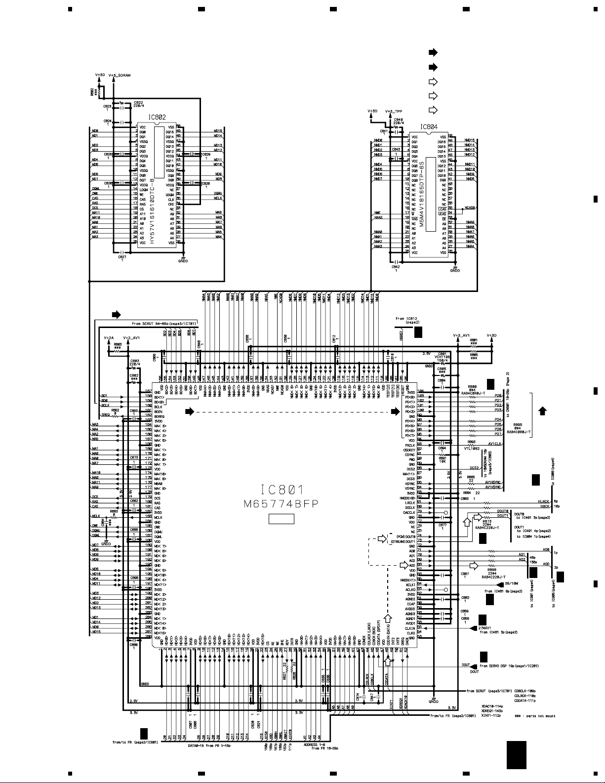
5
16M SDRAM
678
DV-47A, DV-S733A, DV-747A
(V)
: RF (VIDEO) SIGNAL ROUTE
(VD)
: VIDEO DATA SIGNAL ROUTE
(AD)
: AUDIO DATA SIGNAL ROUTE
: AUDIO SIGNAL ROUTE
(D)
: AUDIO (DIGITAL) SIGNAL ROUTE
1M×16 EDO DRAM
A
B
(VD)
(VD) (VD)
AV-1
(D)
B
2/4
B
2/4
(VD)
B
(D)
(D)
B
2/4, 4/4
4/4
B
4/4
B
C
4/4
B
2/4
B
2/4
B
1/4
D
B
2/4
3/4
B
5
6
7
8
29
Page 30
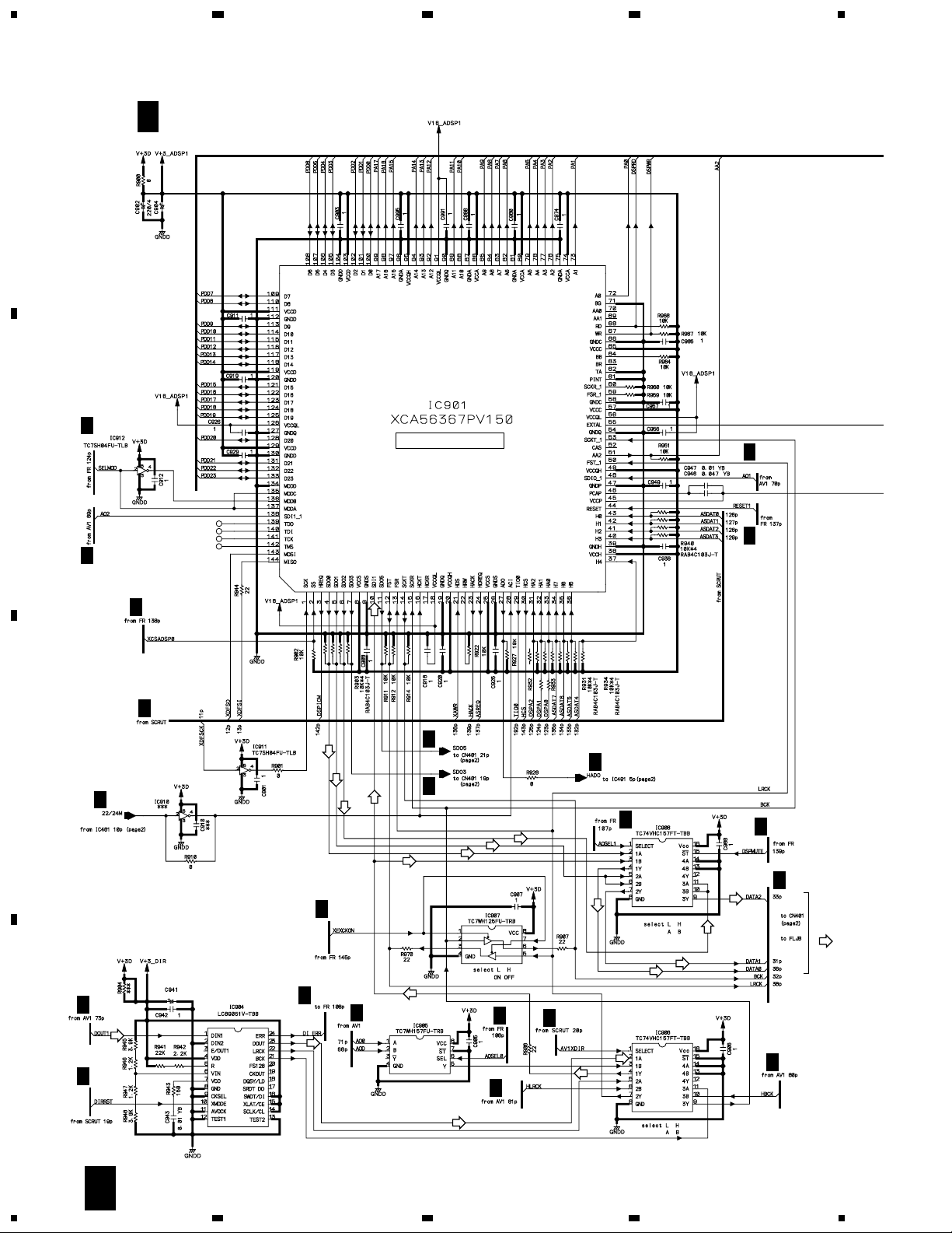
1
23
DV-47A, DV-S733A, DV-747A
3.6 DVDM ASSY (4/4)
4
B 4/4
A
B
2/4
B
B
3/4
DVDM ASSY (VWS1471)
150/4
VCH1195
DVD-AUDIO DSP
B
3/4
B
2/4
B
2/4
B
3/4
(D)
C
B
2/4
B
B
3/4
(D)
D
B
3/4
150/4
(D)
B
2/4
(D)
2/4
(D)
(D)
22
22
B
2/4
B
2/4
B
2/4
(D)
(D)
(D)
(D)
(D)
(D)
B
3/4
(D)
B
2/4
B
3/4
B
3/4
(D)
(D)
(D)
B
2/4
(D)
(D)
(D)
(D)
B
2/4
B
2/4
(D)
B
3/4
30
4/4
B
1234
Page 31
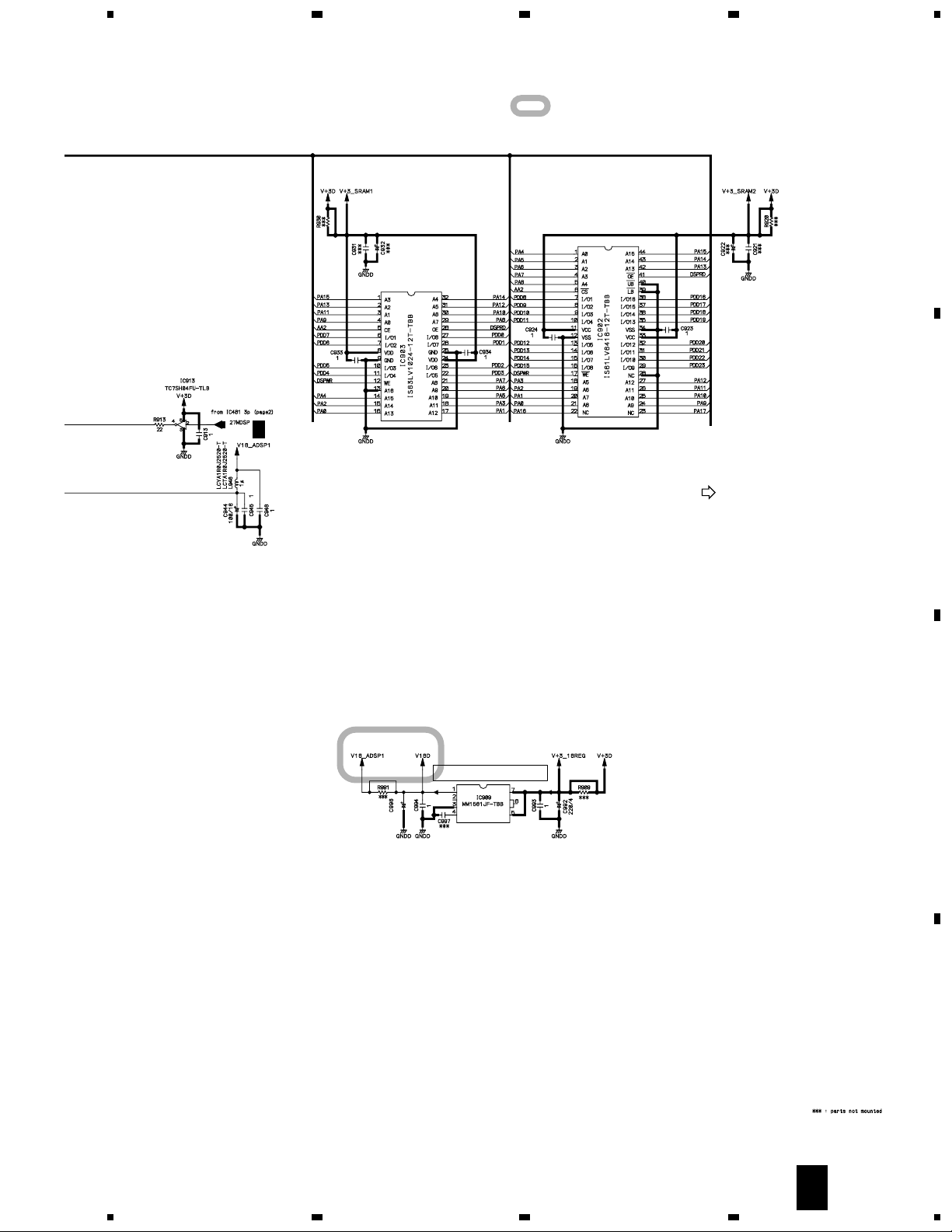
5
678
DV-47A, DV-S733A, DV-747A
: The power supply is shown with the marked box.
A
B
2/4
B
(D)
: AUDIO (DIGITAL) SIGNAL ROUTE
1.8V REGULATOR
150/4
4/4
B
5
6
7
8
31
C
D
Page 32
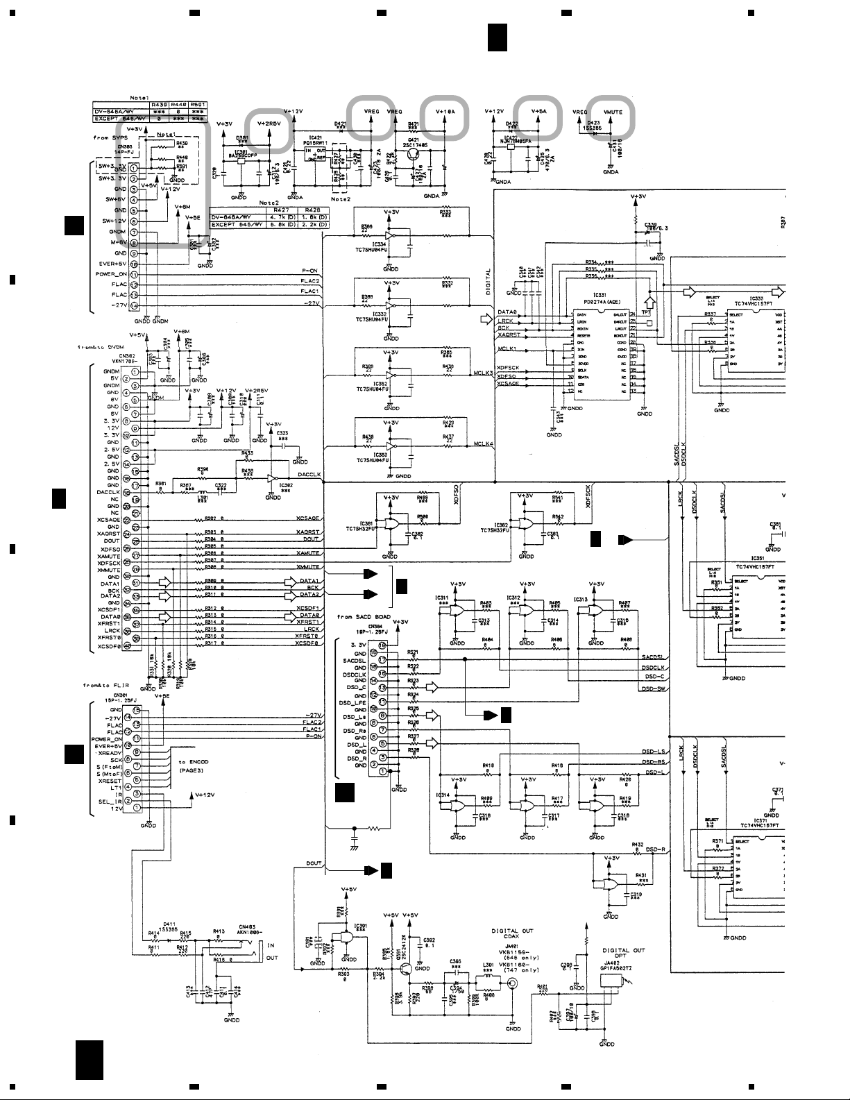
1
23
DV-47A, DV-S733A, DV-747A
3.7 AVJB ASSY (1/3)
C 1/3
4
AVJB ASSY
(KUXJ/CA : VWV1874)
(LBXJ : VWV1877)
(WLXJ/NC, WLXJ/RD : VWV1875)
(WYXJ : VWV1876)
A
B
H
CN101
B 2/4
CN401
1
C321
1
C307
(D) (D)
(D) (D)
(D) (D)
MCLK1
DCLK1
DCLK1
DCLK1
DACCLK
BCK
C422
1
DACCLK
BCK
1
ZA
1
C429
220/16
C428
R435
22
R434
22
MCLK2
MCLK1
(D)
C335
1
C332
1
C352
1
C354
1
C
2/3
C424
R329
(L329)
VTL1084
C331
1
(D)(D)
(D)
2/3
DCLK1
DCLK1
C
C
(D)
(D)
(D)
SACDSL
C
2/3
E
CN101
33M
J
CN901
33M
R1057
C1057
0
∗∗∗
GNDD
33M
D
32
C
1/3
1234
33M
C
2/3
V+5V
R473
(L473)
VTL1084
Page 33
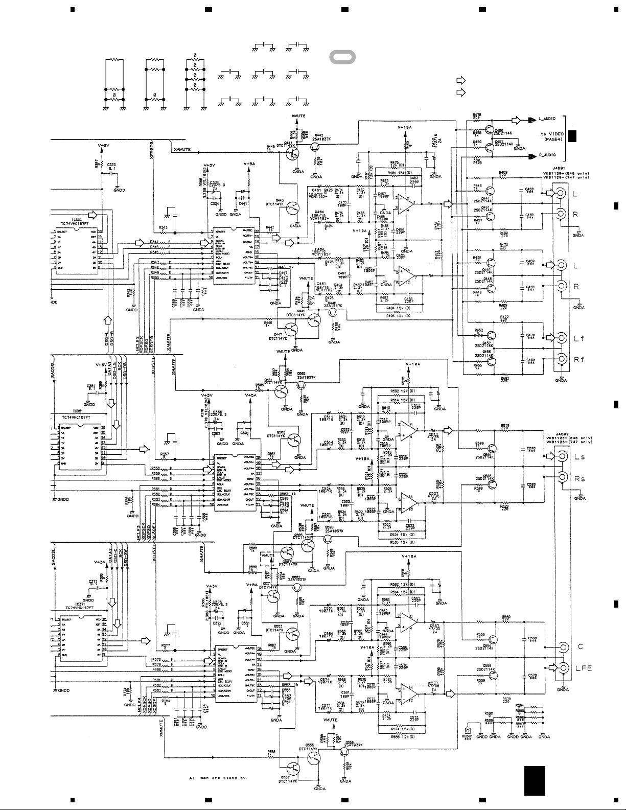
R1041
R1044
R1045
GNDD GNDD
∗∗∗
5
R1046
R1047
R1050
GNDD GNDD
∗∗∗∗∗∗
∗∗∗
R1051
R1052
R1053
R1054
GNDD GNDD
C2041
1
GNDD GNDD
C1055
0.01
GNDD GNDD
C442
470/6.3
ZA
678
C1049
1
GNDD GNDD
C1048
1
GNDD GNDD
C2042
1
GNDD GNDD
R441
(L441)
VTL1084
C1041
0.1
GNDD GNDD
C1042
0.1
GNDD GNDD
C1043
0.1
GNDD GNDD
: The power supply is shown with the marked box.
1
C475
DV-47A, DV-S733A, DV-747A
(D)
: AUDIO (DIGITAL) SIGNAL ROUTE
: AUDIO SIGNAL ROUTE
C
C451
1
R468
220
3/3
A
(D)
(D)
(D)
(D)
(D)
(D)
GNDD
GNDD
C326
C325
C467
0.01
IC441
CS4392D-KS
(D)
C445
22/50
1
C529
C502
470/6.3
R501
(L501)
ZA
VTL1084
0.01
IC501
CS4392D-KS
VCH1236
IC442
NJM5532MD
IC442
NJM5532MD
VCH1236
IC502
NJM5532MD
C487
C506
R497
220
R477
220
R488
220
R471
220
1
C507
220/16
R491
ZA
220
R518
220
B
(D)
IC502
NJM5532MD
C
C505
22/50
R528
220
(D)
(D)
1
(D)
GNDD
C324
1
C552
470/6.3
ZA
VTL1084
R551(L551)
0.01
IC551
CS4392D-KS
C582
IC552
NJM5532MD
C556
C557
220/16
ZA
R568
220
(D)
IC552
NJM5532MD
R578
C555
22/50
5
6
7
220
C
1/3
33
8
D
Page 34
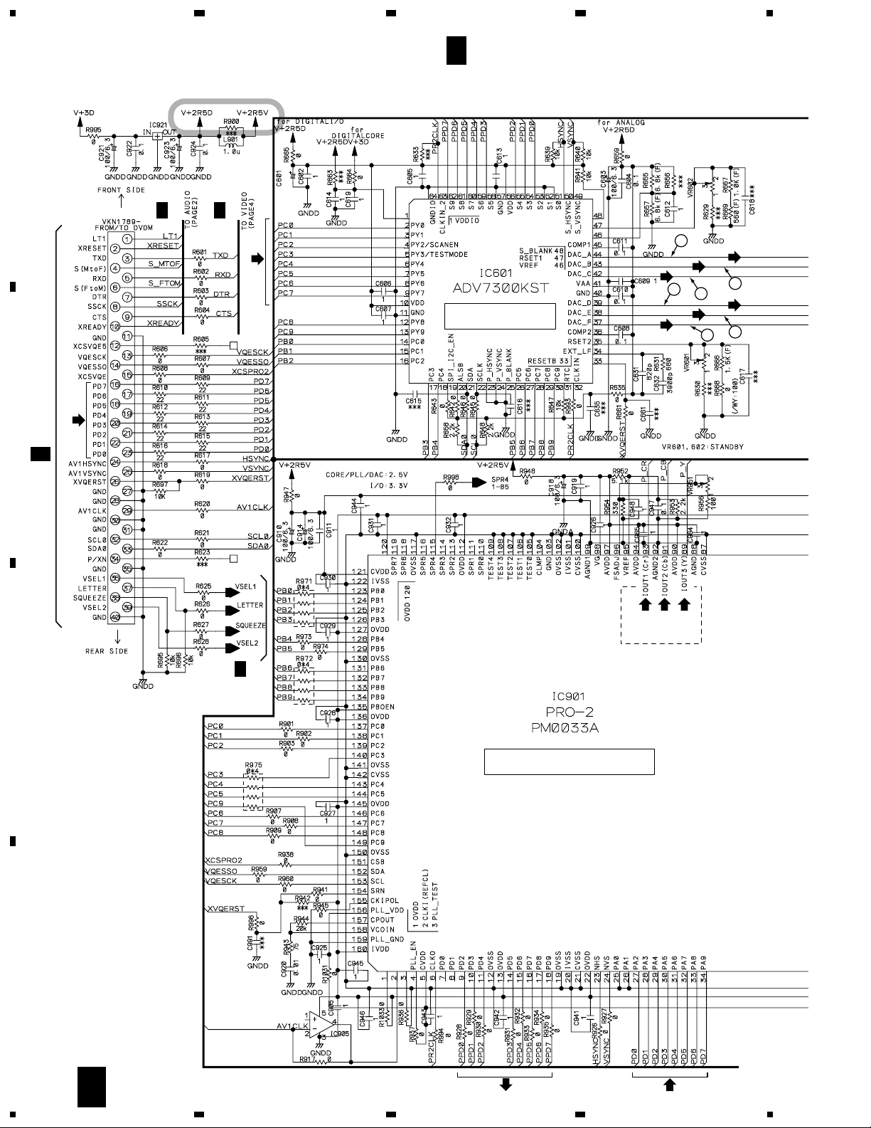
1
DV-47A, DV-S733A, DV-747A
3.8 AVJB ASSY (2/3)
A
CN601
C
1/3
C
3/3
23
AVJB ASSY
C 2/3
(KUXJ/CA : VWV1874)
(LBXJ : VWV1877)
(WLXJ/NC, WLXJ/RD : VWV1875)
(WYXJ : VWV1876)
220/6.3 ZA
4
(VD)
12BIT
VIDEO ENCODER
(VD)
CN501
B
1
(C)
5
(Cb/B)
(Cr/R)
(V)
(Y)
2
3
(Y/G)
6
4
B 2/4
(P_Y)
(P_Cr)
(P_Cb)
WYXJ ONLY
C
3/3
C
PROGRESSIVE & HI-QUALITY
VIDEO ENCODER
D
34
2/3
C
1234
(VD)
(VD)
Page 35
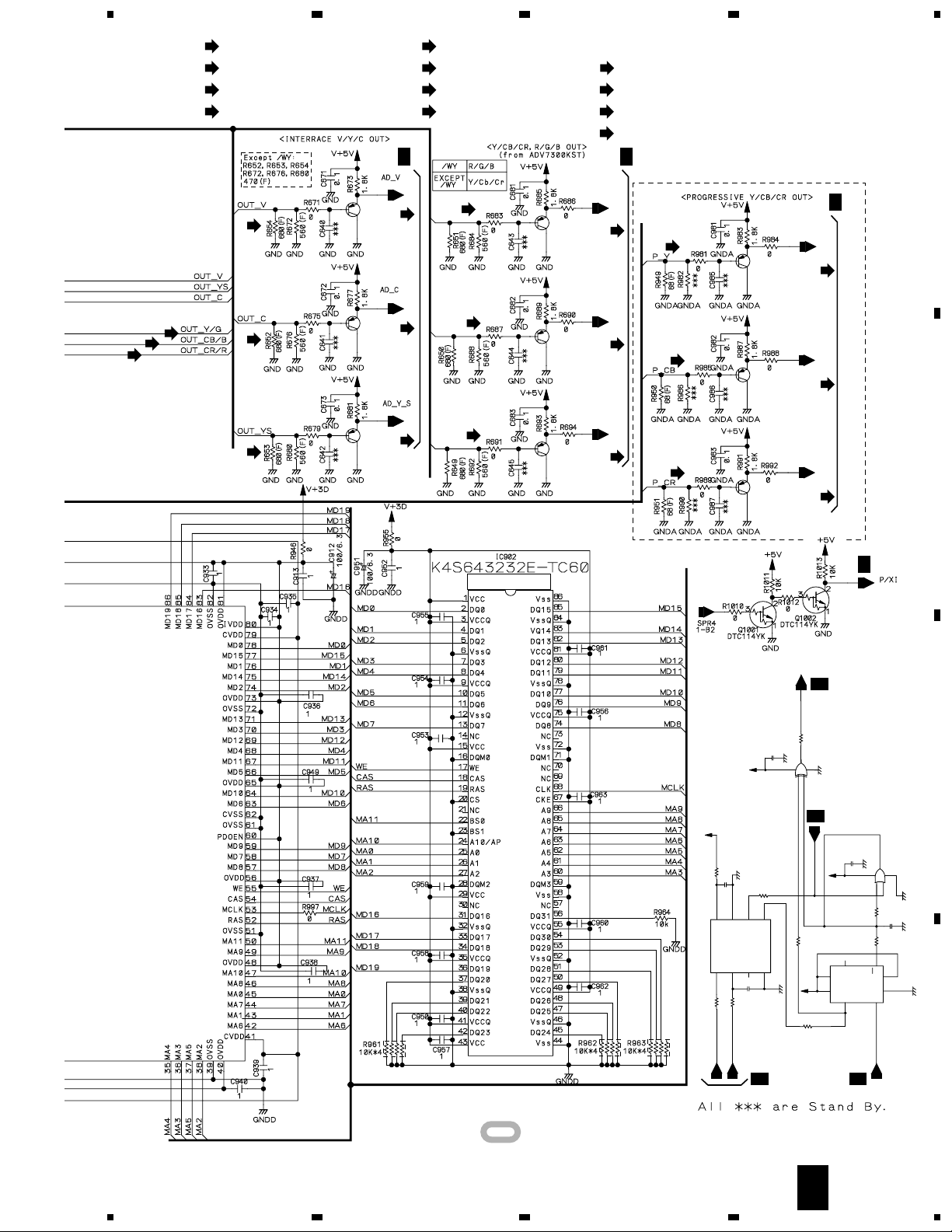
5
(V)
: V SIGNAL ROUTE
(Y)
: Y SIGNAL ROUTE
(C)
: C SIGNAL ROUTE
(VD)
: VIDEO DATA SIGNAL ROUTE
678
(R)
: R SIGNAL ROUTE
(G)
: G SIGNAL ROUTE
(B)
: B SIGNAL ROUTE
(Cb)
: Cb SIGNAL ROUTE
DV-47A, DV-S733A, DV-747A
(Cr)
: Cr SIGNAL ROUTE
(P_Y)
: PROGRESSIVE SCAN VIDEO SIGNAL ROUTE [Y]
(P_Cb)
: PROGRESSIVE SCAN VIDEO SIGNAL ROUTE [Cb]
(P_Cr)
: PROGRESSIVE SCAN VIDEO SIGNAL ROUTE [Cr]
(Cr/R)
(Cb/B)
(Y/G)
(V)
(C)
(Y)
Q601
2SA1037K
Q602
2SA1037K
Q603
2SA1037K
(V)
(C)
(Y)
C
3/3
C
3/3
A
WYXJ ONLY
(P_Y/G)
P_Y/G
(P_Cb/B)
P_CB/B
(P_Cr/R)
P_CR/R
64M SDRAM
Q604
2SA1037K
Q605
2SA1037K
Q606
2SA1037K
P_Y/G
(P_Y/G)
P_CB/B
(P_Cb/B)
P_CR/R
(P_Cr/R)
(P_Y)
(P_Cb)
(P_Cr)
Q981
2SA1037K
Q982
2SA1037K
Q983
2SA1037K
PR2_Y
(P_Y)
PR2_CB
(P_Cb)
PR2_CR
(P_Cr)
C
3/3
B
C
3/3
V+3V
L1512
VTL1084
1
C1506
876
123
R1505 0
R1518 0
DACCLK
33M
V+3V
IC1505
TC7WH157FU
∗∗∗
C1515
R1514
5
4
1/3
C
C1504
0
DCLK1
R1506
0.1
5
1
IC1502
TC7SH86FU
0
R1505
4
V+3V
R1516
1/3
C
22
23
1/3
C
SACDSL
86
0
V+3V
C
C1503
0.1
IC1503
TC7SH32FU
4
5
1
23
33k
C1501
0.1
R1502
10k
R1501
5
3
QD
Q
7
IC1501
TC7WH74FU
1/3
C
1
BCK
4
D
2
: The power supply is shown with the marked box.
2/3
C
5
6
7
8
35
Page 36
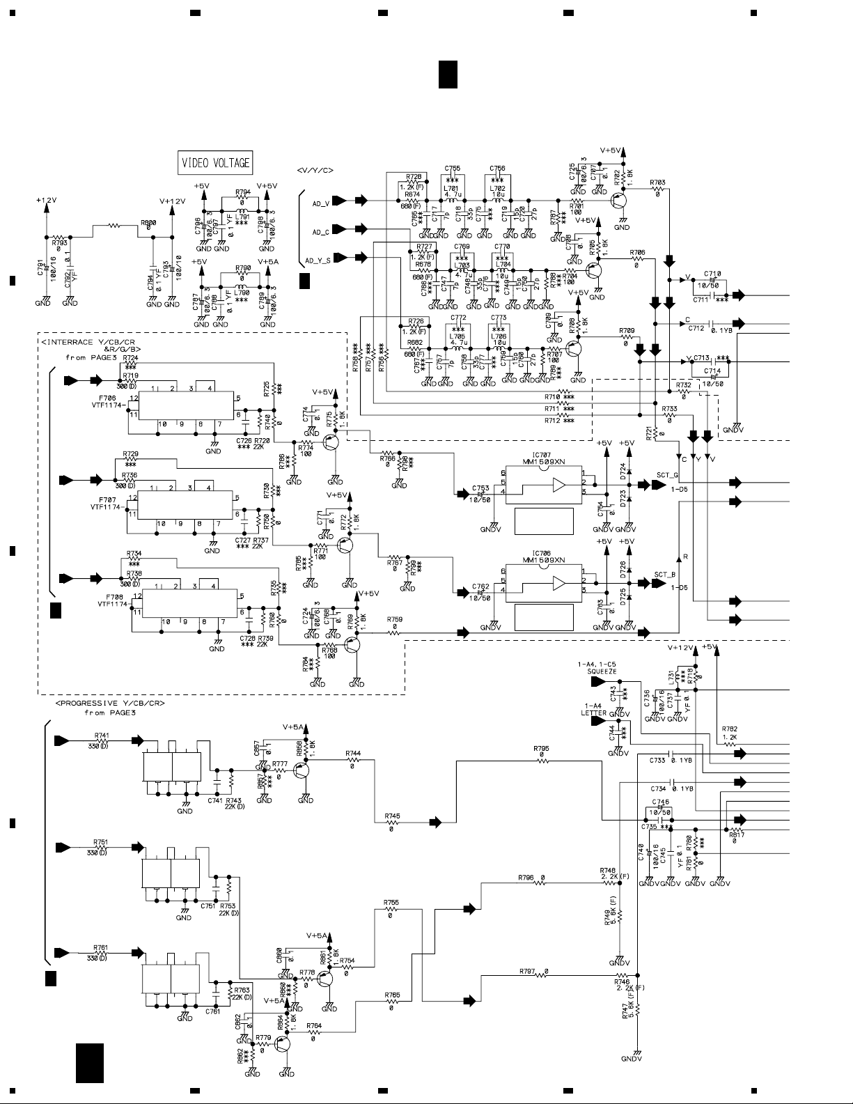
1
23
DV-47A, DV-S733A, DV-747A
4
3.9 AVJB ASSY (3/3)
A
WYXJ ONLY
(G)
P_Y/G
B
(B)
P_CB/B
C 3/3
(KUXJ/CA : VWV1874)
(LBXJ : VWV1877)
(WLXJ/NC, WLXJ/RD : VWV1875)
(WYXJ : VWV1876)
AVJB ASSY
(V)
(C)
(Y)
C
2/3
Q703
2SA1037K
Q774
2SA1037K
(G)
6dB, 75Ω
DRIVER
Q702
2SA1037K
Q701
2SA1037K
(Y)
(G)
(C)(C)
(V)
(V)
(V)
(C)
(V)
(Y)
(C)
(R)
Q771
2SA1037K
Q768
2SA1037K
(B)
(R)
WYXJ ONLY
6dB, 75Ω
DRIVER
(B)
(Y)
(V)
(R)
C
(R)
P_CR/R
2/3
C
P_Y/G (Except WYXJ)
PR2_Y (WYXJ Only)
P_CB/B (Except WYXJ)
PR2_CB (WYXJ Only)
P_CR/R (Except WYXJ)
PR2_CR (WYXJ Only)
F721
VTF1175
F722
VTF1175
(P_Y)
(P_Cb)
(P_Cr)
18p
18p
Q706
2SA1037K
(Cb)
(Cr)
(Y)
(Cr)
(Y)
D
2/3
F723
VTF1175
18p
Q707
2SA1037K
(Cb)
C
36
Q708
2SA1037K
C
3/3
1234
Page 37
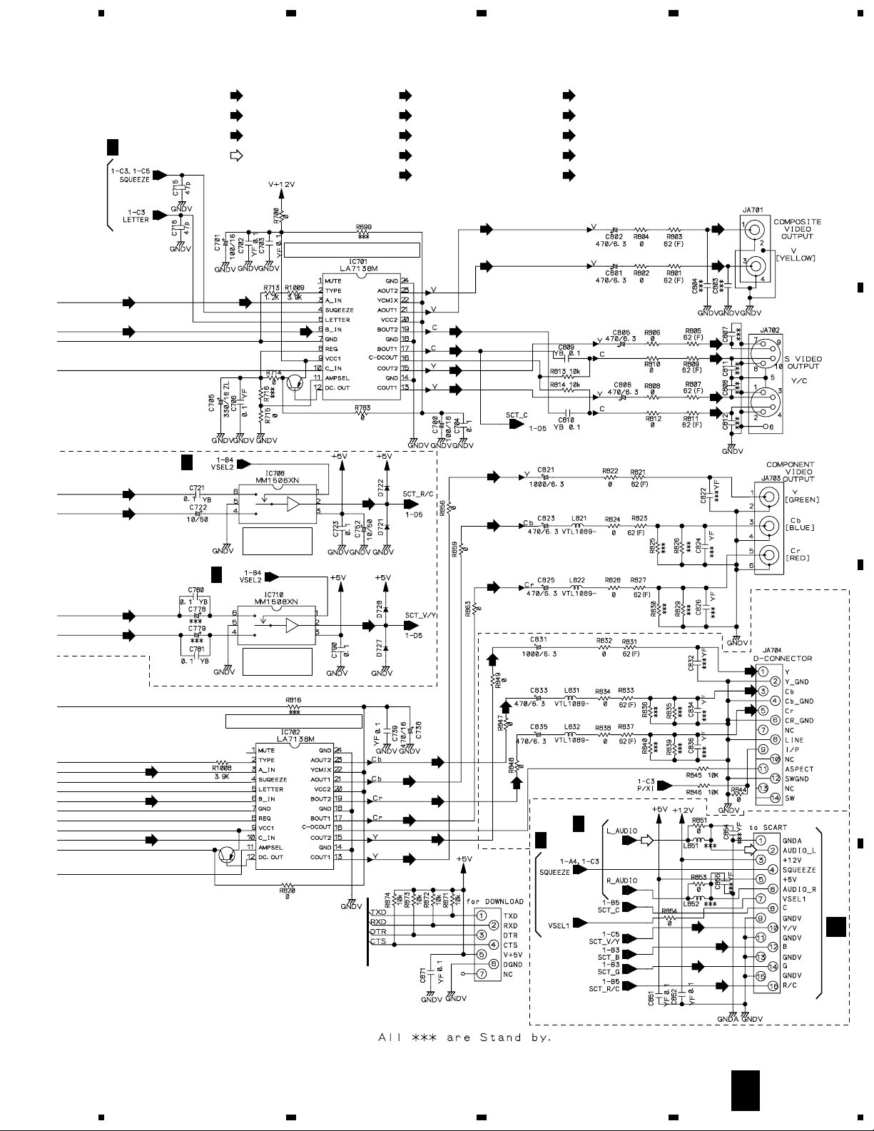
5
678
DV-47A, DV-S733A, DV-747A
C
2/3
(V)
(C)
WYXJ ONLY
(C)
(R)
(V)
: V SIGNAL ROUTE
(Y)
: Y SIGNAL ROUTE
(C)
: C SIGNAL ROUTE
: AUDIO SIGNAL ROUTE
3 IN 6 OUT VIDEO AMP.
(V)
(C)
Q704
2SA1037K
C
2/3
(R/C)
(R)
: R SIGNAL ROUTE
(G)
: G SIGNAL ROUTE
(B)
: B SIGNAL ROUTE
(Y/V)
: Y/V SIGNAL ROUTE
(R/C)
: R/C SIGNAL ROUTE
(C)
(C)
(Cb)
: Cb SIGNAL ROUTE
(Cr)
: Cr SIGNAL ROUTE
(P_Y)
: PROGRESSIVE SCAN VIDEO SIGNAL ROUTE [Y]
(P_Cb)
: PROGRESSIVE SCAN VIDEO SIGNAL ROUTE [Cb]
(P_Cr)
: PROGRESSIVE SCAN VIDEO SIGNAL ROUTE [Cr]
(V)
(V)
(Y)
(Y)
(Y)
(Cb)
(V)
(V)
(Y)
(C)
(Y)
(C)
A
B
6dB, 75Ω
SW DRIVER
C
2/3
(Y)
(V)
6dB, 75Ω
SW DRIVER
(Y/V)
(Cr)
Except
KUXJ/CA,
WYXJ
(Cb)
(Cr)
(Y)
C
(Y)
(Cb)
3 IN 6 OUT VIDEO AMP.
(Cb)
(Cb)
(Cr)
(Y)
Q705
2SA1037K
(Cb)
(Cr)
(Cr)
(Y)
(Y)
(Cr)
C
1/3
C
2/3
CN702
CN703
CN101
(Y/V)
(G)
(B)
(R/C)
D
D
WYXJ ONLY
3/3
C
5
6
7
8
37
Page 38
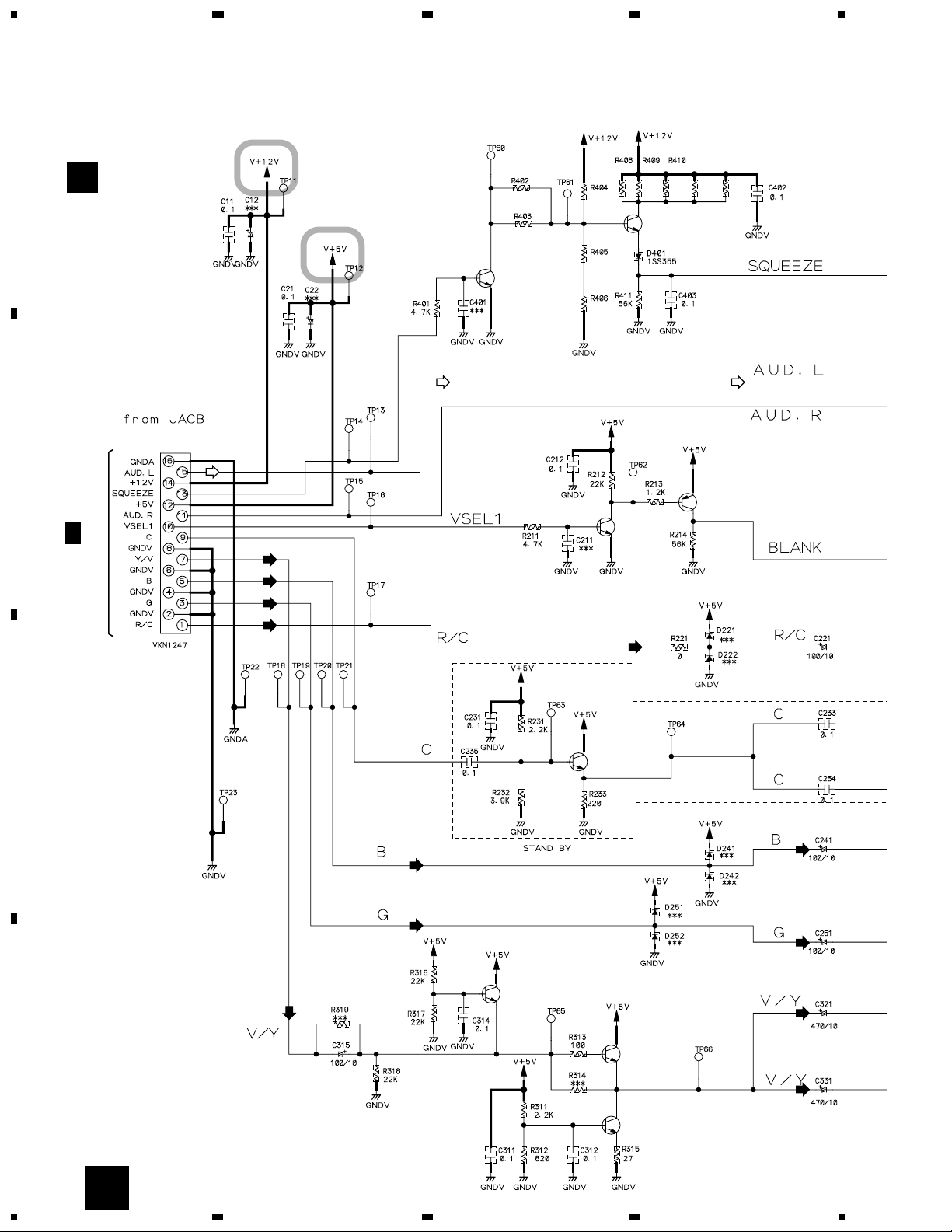
1
23
DV-47A, DV-S733A, DV-747A
3.10 SCRB ASSY [WYXJ TYPE ONLY]
A
SCRB ASSY
D
(VWV1850)
15k 10k
∗∗∗
1.8k 1.8k 1.8k
Q403
2SC2412K
R421
1.8k
4
R422
1.8k
Q401
2SC2412K
∗∗∗
∗∗∗
CN101
B
Q403
2SA1037K
Q401
C 3/3
CN702
(Y/V)
(B)
(G)
(R/C)
2SC2412K
(R/C)
Q401
C
(B)
(G)
Q401
(Y/V)
2SC2412K
2SC2412K
Q401
2SC2412K
(B)
(G)
(Y/V)
D
(Y/V)
Q401
2SC2412K
38
D
1234
Page 39
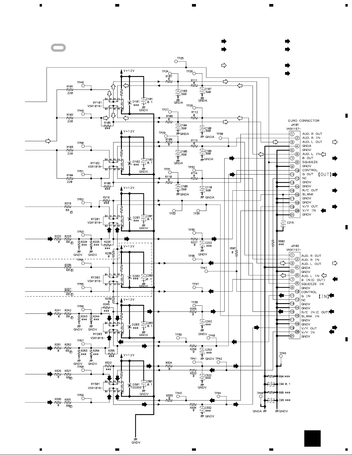
5
678
DV-47A, DV-S733A, DV-747A
: The power supply is shown with the marked box.
0
R191
0
R192
0
R201
(V)
: V SIGNAL ROUTE
(Y)
: Y SIGNAL ROUTE
: AUDIO SIGNAL ROUTE
(B)
(G)
(Y/V)
: Y/V SIGNAL ROUTE
(R/C)
: R/C SIGNAL ROUTE
(G)
: G SIGNAL ROUTE
(B)
: B SIGNAL ROUTE
(R/C)
(Y/V)
(Y/V)
(G)
A
(B)
B
(R/C) (R/C) (R/C)
(B)
(G)
(Y/V)
(R/C)
(B)
(G)
(Y/V)
(R/C)
(B)
(Y/V)
(G)
R202
R203
R301
∗∗∗
0
0
(G)
(B)
(Y/V)
(B)
(R/C)
(B)
(Y/V)
(Y/V)
0.1
(G)
(R/C)
(Y/V) (Y/V)
(G)
(B)
C
(G)
(R/C)
(V/Y)
(Y/V)
(Y/V)
(Y/V)
5
(Y/V) (Y/V)
6
(Y/V)
D
7
8
39
D
Page 40
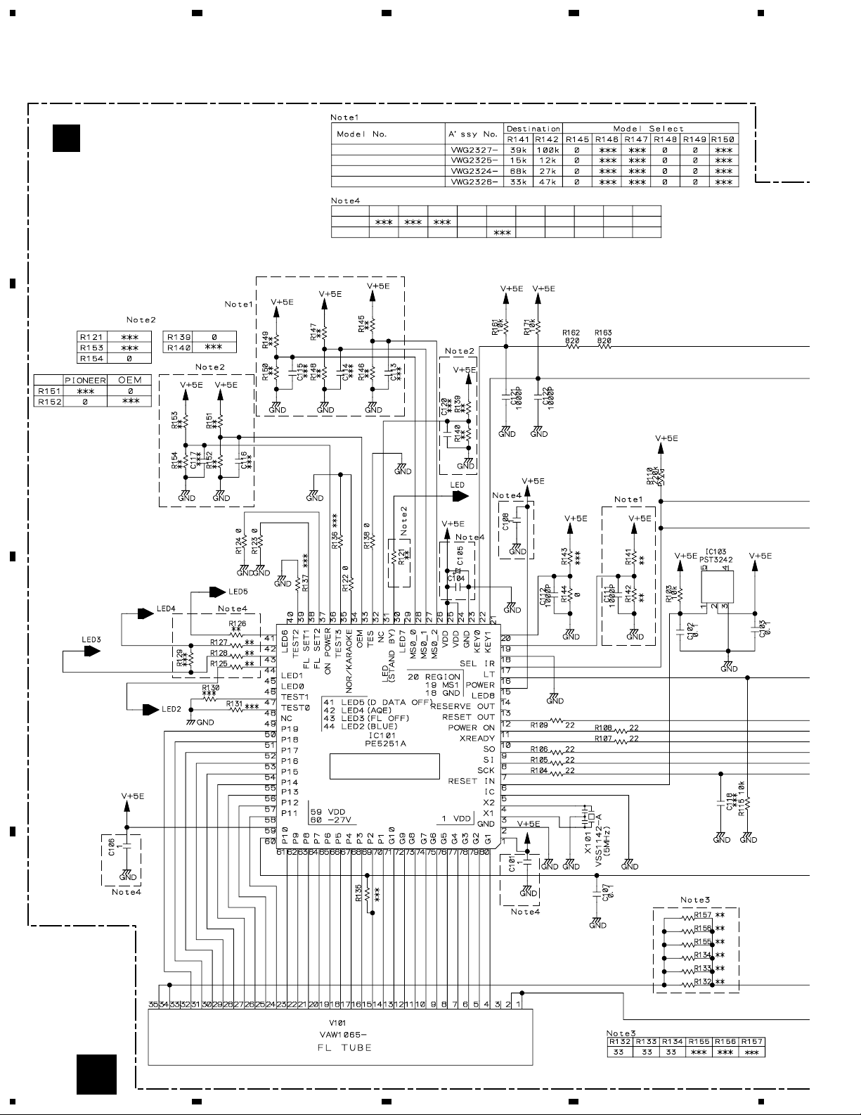
1
23
DV-47A, DV-S733A, DV-747A
3.11 FLIR, PWSB, KEYB and DILB ASSYS
FLIR ASSY
A
B
E
(KUXJ/CA : VWG2327)
(LBXJ : VWG2325)
(WLXJ/NC : VWG2324)
(WLXJ/RD : VWG2324)
(WYXJ : VWG2326)
DV-47A/KUXJ/CA
DV-S733A/LBXJ
DV-S733A/WLXJ/RD, WLXJ/RD
DV-747A/WYXJ
KUXJ/CA
Others
R125 R126 R127 R128
220
220680 6800
R129 C101 C104 C105 C106 C108
114711
0
114711
4
C
FL CONTROL
MICROCOMPUTER
D
40
E
1234
Page 41
5
678
DV-47A, DV-S733A, DV-747A
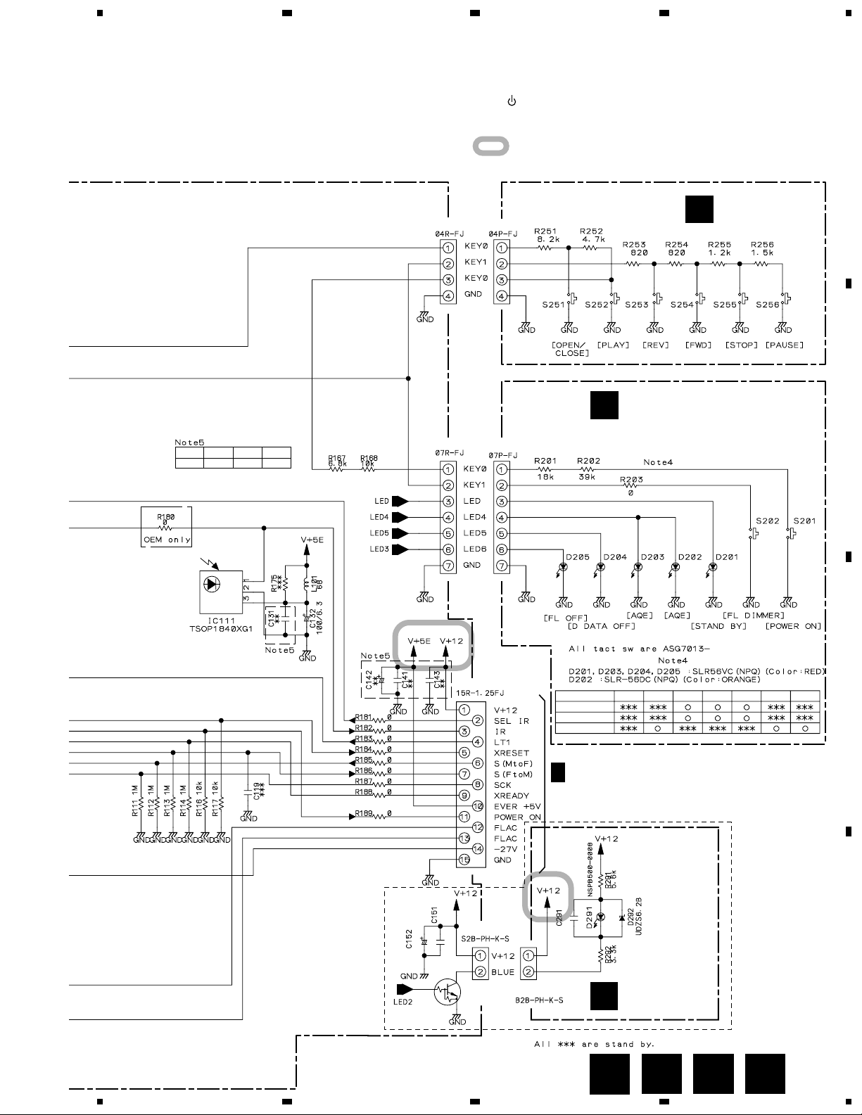
C131 C141 C142 C143
1 1 47 0.22
KEYB ASSY
S251 : 0 (OPEN/CLOSE)
S252 : 3 (PLAY)
S253 : 41
S254 : 41
S255 : 7 (STOP)
S256 : 8 (PAUSE)
PWSB ASSY
S201 : POWER STANDBY/ON
S202 : FL DIMMER
: The power supply is shown with the marked box.
KEYB ASSY
G
CN251CN103
PWSB ASSY
(KUXJ/CA : VWG2312)
F
(LBXJ : VWG2310)
CN201CN102
(WLXJ/NC, WLXJ/RD : VWG2310)
(WYXJ : VWG2311)
(VWG2306)
A
B
CN101
Assy No.
VWG2310
VWG2311
VWG2312
D201 D202 D203 D204 D205 S202 R203
C
C 1/3
CN301
Except KUXJ/CA
0.22
CN104
47/16
Q101
DTC124EK
5
6
CN291
1
D
DILB ASSY
I
(VWG2322)
41
E
7
IGF
8
Page 42
1
23
DV-47A, DV-S733A, DV-747A
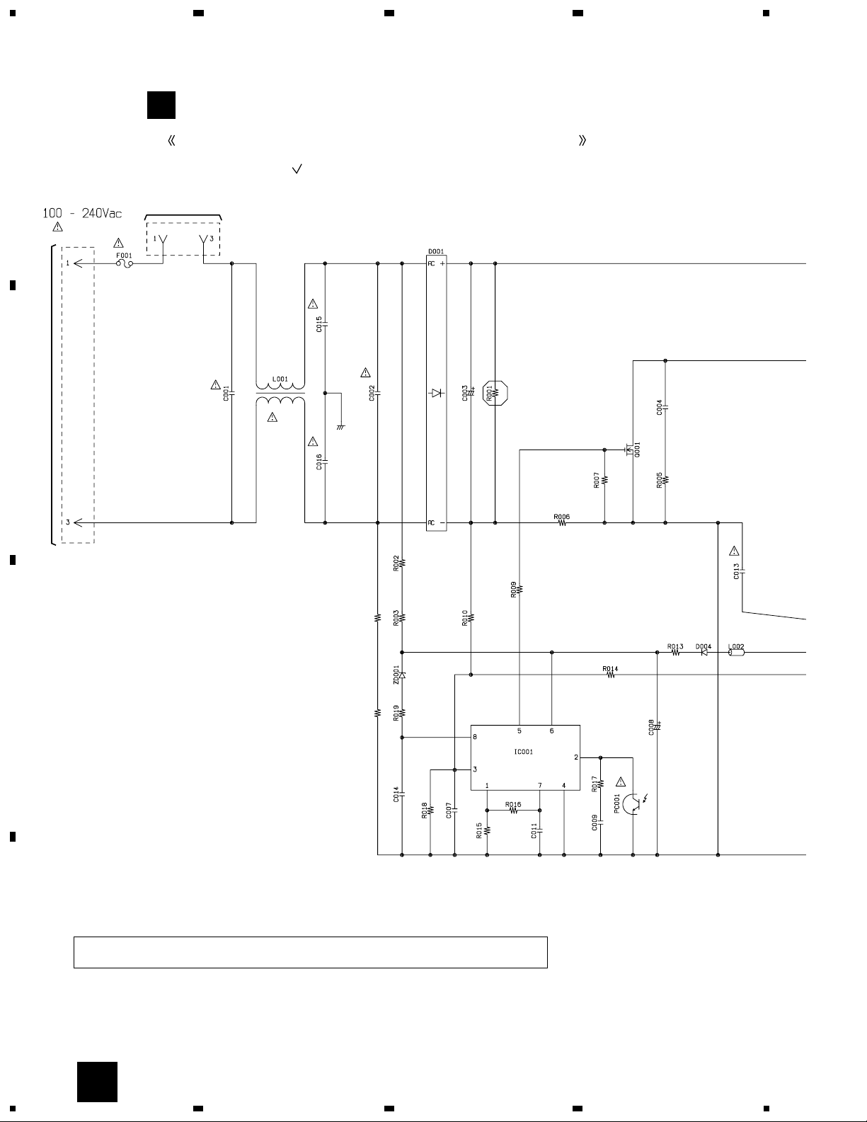
3.12 POWER SUPPLY UNIT (VWR1346)
POWER SUPPLY UNIT (VWR1346)
H
4
A
CN001
1.25A
REK1099
NOTE OF SPARE PARTS IN POWER SUPPLY (SYPS) UNIT
• In case of repairing, use the described parts only to prevent an accident.
• Please write the red mark on the board when the primary section of POWER SUPPLY (SYPS) Unit is repaired.
• Please take care to keep the space, not touching other parts when replacing the parts.
Short
CN002
AC IN
B
R020R021
C
• NOTE FOR FUSE REPLACEMENT
CAUTION -
D
FOR CONTINUED PROTECTION AGAINST RISK OF FIRE.
REPLACE WITH SAME TYPE AND RATINGS ONLY.
42
H
1234
Page 43
5
678
DV-47A, DV-S733A, DV-747A
A
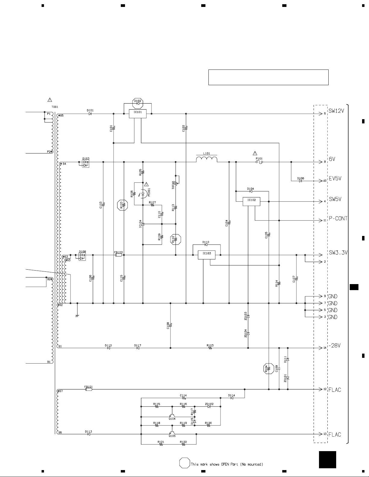
CAUTION : FOR CONTINUED PROTECTION AGAINST RISK OF FIRE.
REPLACE ONLY WITH SAME TYPE NO. 49101.6 MFD,
BY LITTELFUSE INC. FOR P101 (AEK7066).
CN101
1.6A
AEK7066
B
CN303
C 1/3
C
D
H
5
6
7
8
43
Page 44
1
DV-47A, DV-S733A, DV-747A
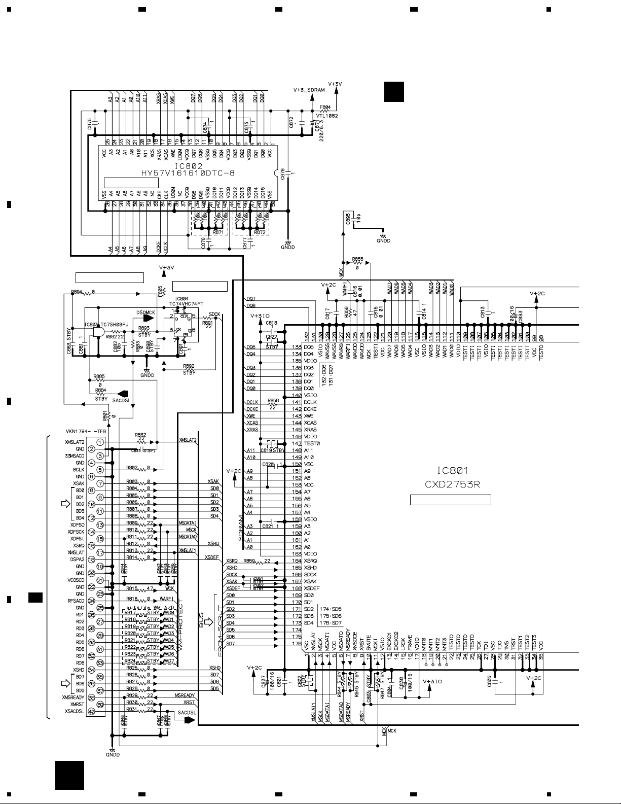
3.13 SACD ASSY
A
16M SDRAM
23
SACD ASSY
J
(VWG2331)
4
MCK INVERTER
B
CN801
C
(AD)
SDCK DELAY
VTL1082
SACD DECORDER
CN602
B 2/4
(AD)
(AD)
D
44
J
1234
Page 45
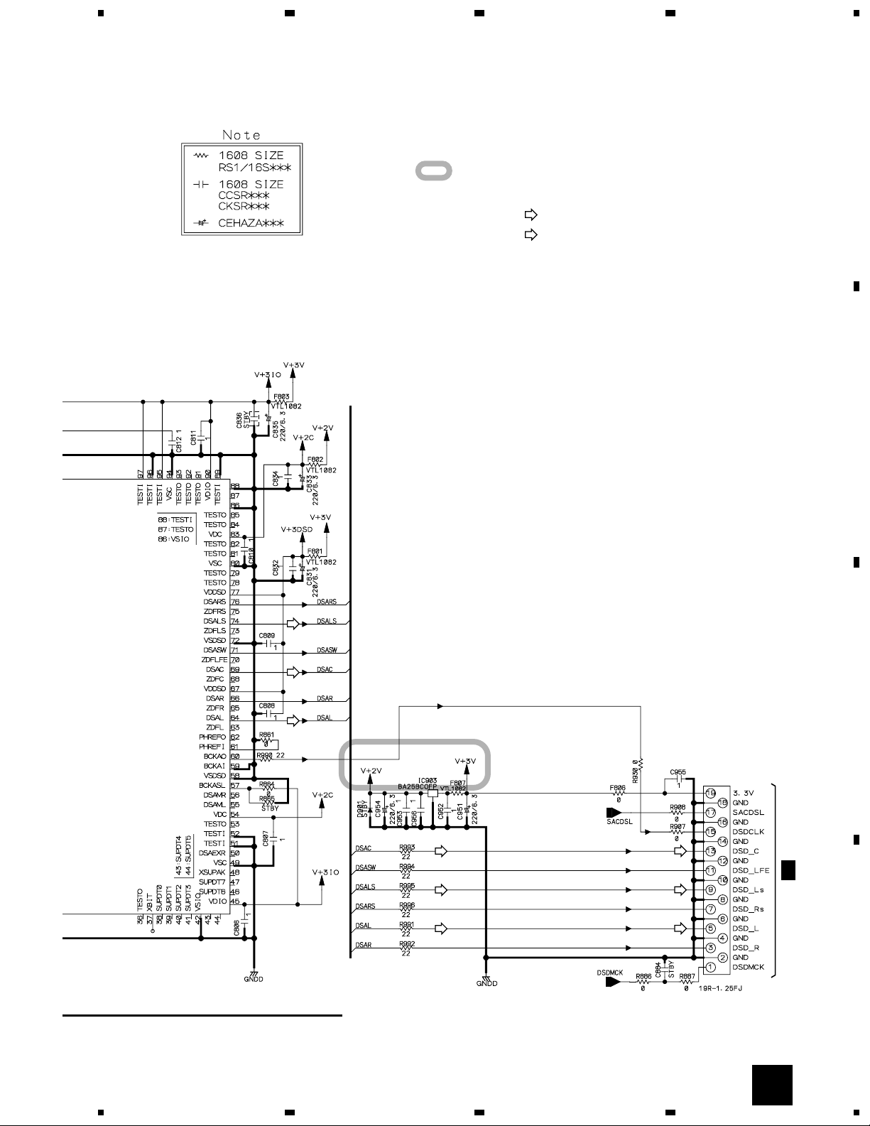
5
678
DV-47A, DV-S733A, DV-747A
A
: The power supply is shown with the marked box.
(AD)
: AUDIO DATA SIGNAL ROUTE
(D)
: AUDIO (DIGITAL) SIGNAL ROUTE
B
(D)
(D)
(D)
(D)
(D)
(D)
(D)
(D)
(D)
CN901
C
C 1/3
CN304
D
J
5
6
7
8
45
Page 46
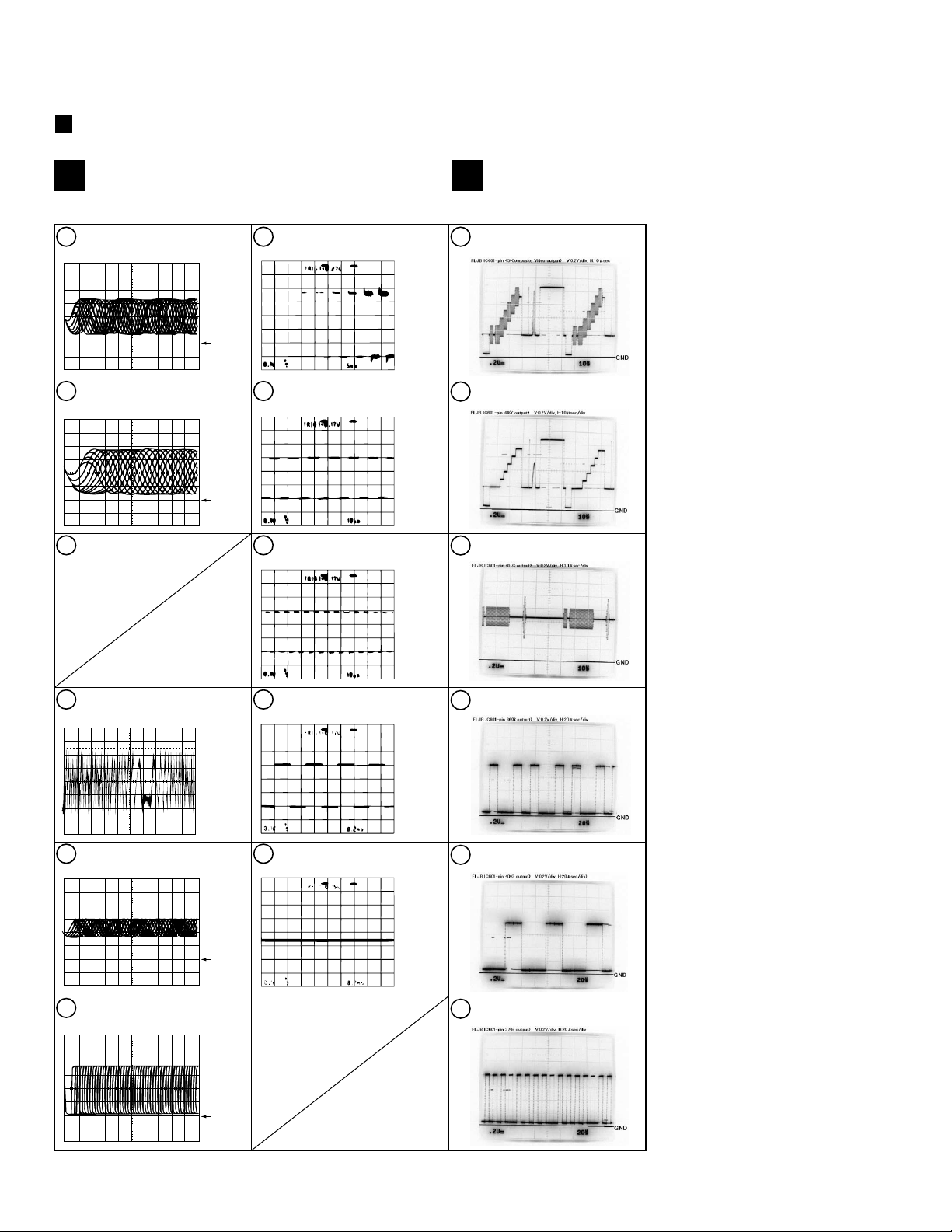
DV-47A, DV-S733A, DV-747A
WAVEFORMS
Note : The encircled numbers denote measuring point in the schematic diagram.
DVDM ASSY
B
Measurement condition
Foot of R104 (RF)
1
V: 100mV/div. H: 0.2µsec/div.
Q106-emitter (RFO)
2
V: 500mV/div. H: 0.1µsec/div.
3
: No. 1 to 4 and 6 to 11 : MJK1, Title 1-chp 1
No. 5 : CD, ABEX-784 Track 1
IC251 - pin 24 (FG)
7
V: 1V/div. H: 5msec/div.
GND
Foot of R261 (FPWM)
8
V: 1V/div. H: 5msec/div.
GND
Foot of R262 (VPWM)
9
V: 1V/div. H: 5msec/div.
AVJB ASSY
C
Measurement condition
IC601 - pin 44
1
(Composite Video output)
V: 0.2V/div. H: 10µsec/div.
IC601 - pin 43 (Y output)
2
V: 0.2V/div. H: 10µsec/div.
IC601 - pin 42 (C output)
3
V: 0.2V/div. H: 10µsec/div.
: No. 1 to 3 : MJK1, Title 1-chp 4
No. 4 to 6 : T2-19, Color-bar
IC101-pin 35 (Tracking Error)
4
(AI-Inner Tracking Off)
V: 500mV/div. H: 2msec/div.
IC201 - pin 39 (EFM before slice)
5
V: 1V/div. H: 1µsec/div.
IC201 - pin 1 (EFM)
6
V: 1V/div. H: 0.2µsec/div.
GND
GND
Foot of R263 (PPWM)
10
V: 1V/div. H: 5msec/div.
Foot of R264 (RPWM)
11
V: 1V/div. H: 5msec/div.
IC601 - pin 37 (R output)
4
V: 0.2V/div. H: 20µsec/div.
IC601 - pin 39 (G output)
5
V: 0.2V/div. H: 20µsec/div.
IC601 - pin 38 (B output)
6
V: 0.2V/div. H: 20µsec/div.
46
Page 47
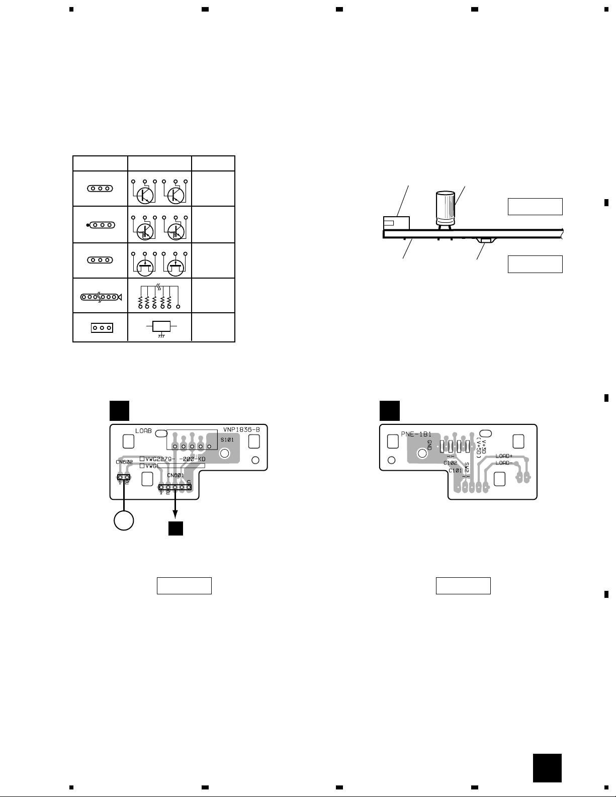
1
SIDE A SIDE B
(VNP1836-B)
(VNP1836-B)
CN103
B
LOAB ASSY
A
LOAB ASSY
A
LOADING
MOTOR
ASSY
M
NOTE FOR PCB DIAGRAMS :
1. Part numbers in PCB diagrams match those in the schematic
diagrams.
2. A comparison between the main parts of PCB and schematic
diagrams is shown below.
3. The parts mounted on this PCB include all necessary parts for
several destinations.
For further information for respective destinations, be sure to
check with the schematic diagram.
4. View point of PCB diagrams.
Symbol In PCB
Diagrams
Symbol In Schematic
Diagrams
Part Name
BCE
D
DGGSS
BCE
BCE
DGS
BCEBCE
BCE
Transistor
Transistor
with resistor
Field effect
transistor
Resistor array
3-terminal
regulator
Capacitor
Connector
P.C.Board
Chip Part
SIDE A
SIDE B
4. PCB CONNECTION DIAGRAM
4.1 LOAB ASSY
234
DV-47A, DV-S733A, DV-747A
A
B
1
C
D
A
2
3
4
47
Page 48
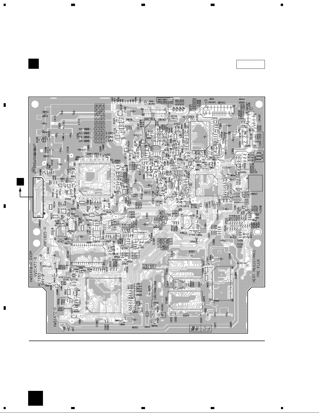
1
DV-47A, DV-S733A, DV-747A
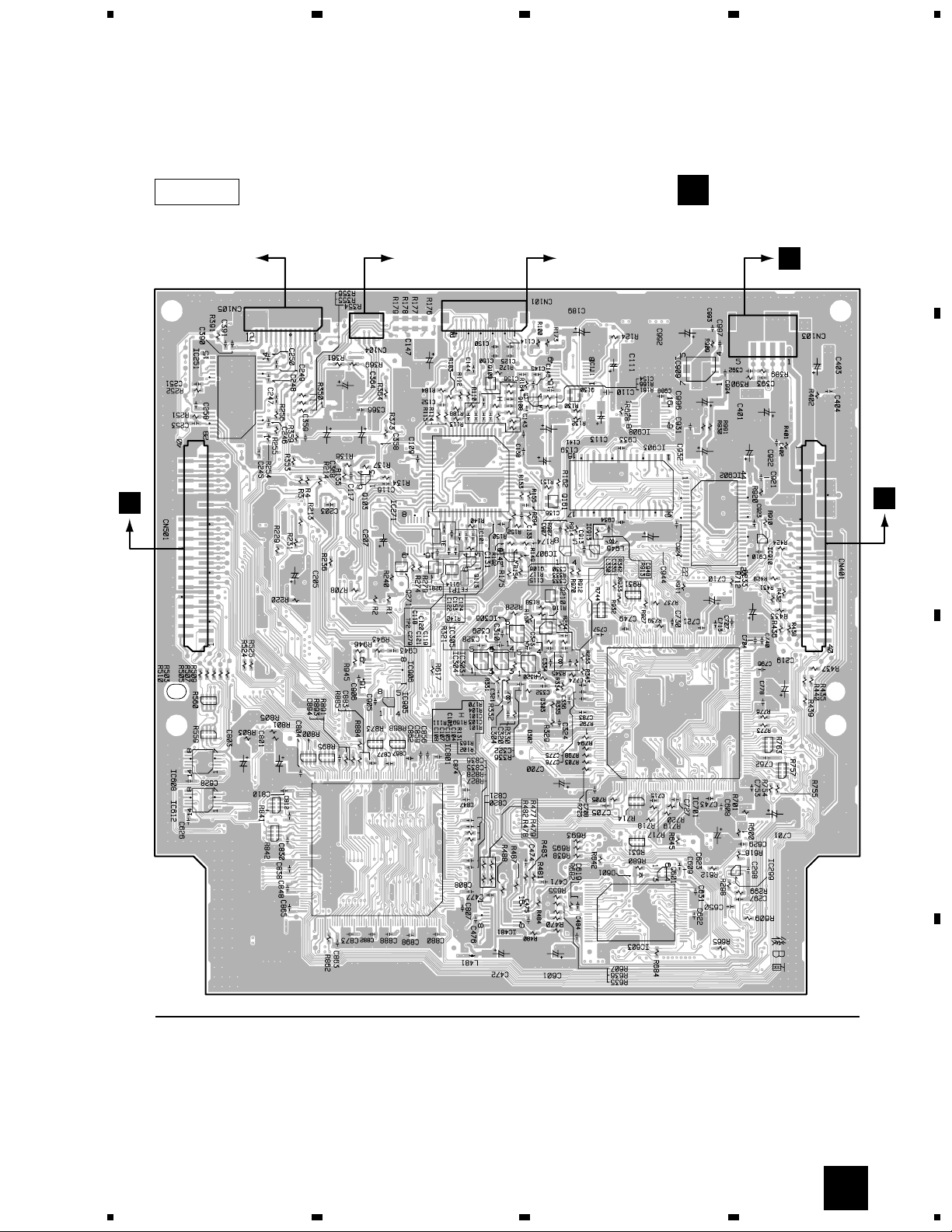
4.2 DVDM ASSY
A
23
4
B
DVDM ASSY
B
SIDE A
CN801
J
C
(VNP1825-A)
IC401 IC911 IC912 IC901 Q101
D
48
IC491
B
1234
IC211 Q571Q542 Q112
IC210 IC702
IC606
IC261
IC601
Q102
Q115
Q118 IC281 IC351 IC532
Q116
Q117
Q111
IC302 IC802
Q291
Q107
Q543
IC291 IC201
Q292
IC904
Q241Q141
IC803
IC804
Page 49
1
234
DV-47A, DV-S733A, DV-747A
A
SIDE B
SPINDLE
MOTOR
CN601
C
STEPPING
MOTOR
(CARRIAGE)
PICKUP
ASSY
B
DVDM ASSY
A
CN601
B
CN302
C
(VNP1825-A)
IC608
IC612
1
IC251 Q103 Q109 Q108 Q130 IC903 IC909 IC910
IC905
IC271
IC101
Q113
IC303IC304
Q142
IC306
Q106
IC305
Q210
IC907
Q601
IC603IC801
3
Q281Q271
2
Q161
IC701
IC902IC913
IC299
B
4
C
D
49
Page 50
1
23
DV-47A, DV-S733A, DV-747A
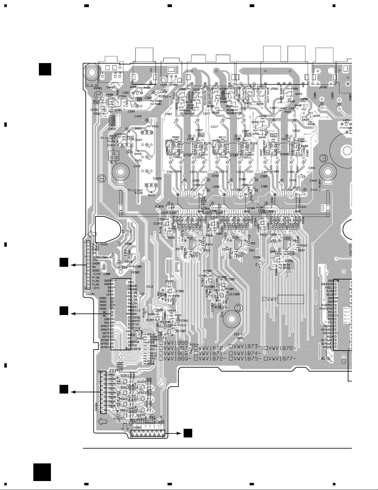
4.3 AVJB ASSY
4
A
C
AVJB
ASSY
B
H
CN101
C
B
CN401
J
CN901
D
CN101
E
50
Q391 Q421 Q554 Q558 Q504 Q508 Q452 Q449 Q444
IC391
C
1234
IC421
IC311
IC313
IC315
IC317 IC362
IC312
IC314
IC316
IC422
IC361
Q552 Q556 Q502 Q506 Q442
IC551
IC302
IC1505
IC371 IC334
IC352IC353
IC1504
IC1501
IC1502
IC1503
IC502 IC442IC552
IC501
IC351
Q441
Q443
IC332
IC441
IC333
Q446
Q445
Q447
Page 51
5
678
DV-47A, DV-S733A, DV-747A
CN101
D
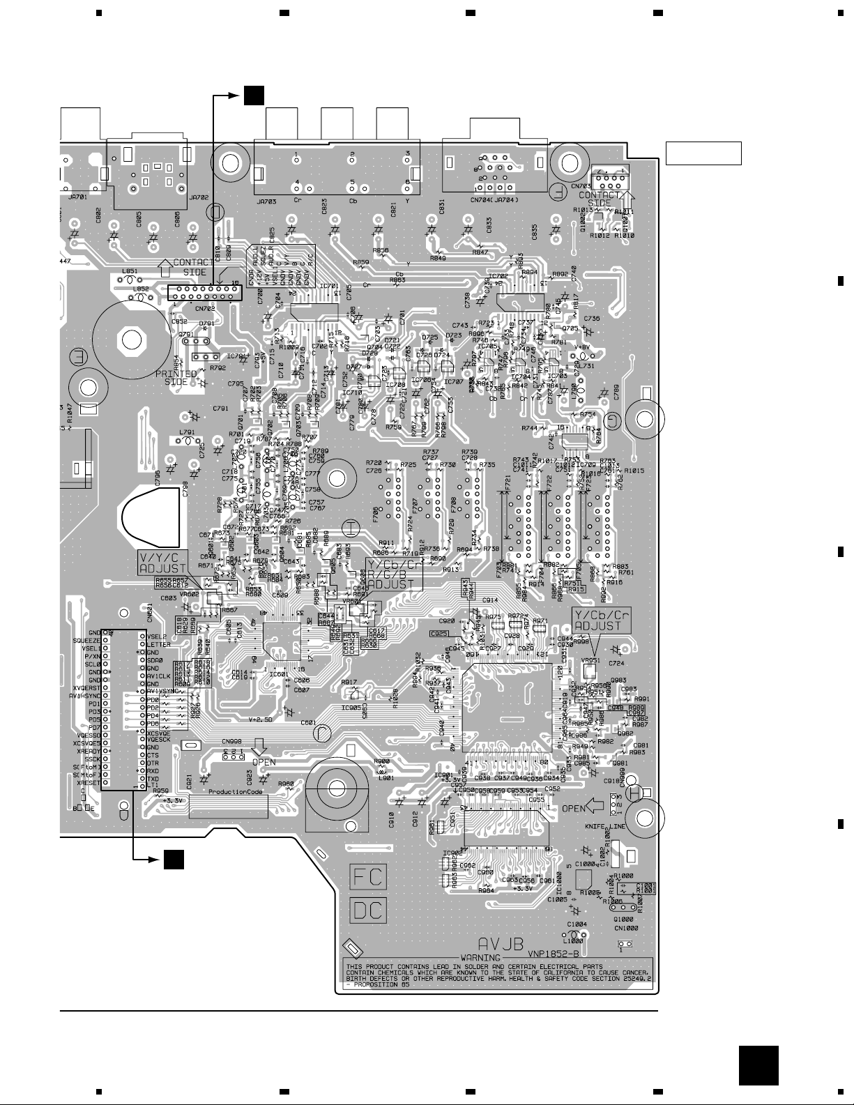
SIDE A
A
B
CN501
B
Q791
VR602 VR601 VR951
IC901
IC902
IC702
IC704
5
IC791
Q701 Q702 Q703
Q603Q602Q601
IC701 Q704
IC601
Q605Q604
IC710 IC708IC706 IC707 IC705 IC703
Q601
IC905
6
Q705
7
IC709
IC1000
Q1002
Q983
Q982
Q981
Q1001
Q1000
(VNP1852-B)
C
8
C
D
51
Page 52
1
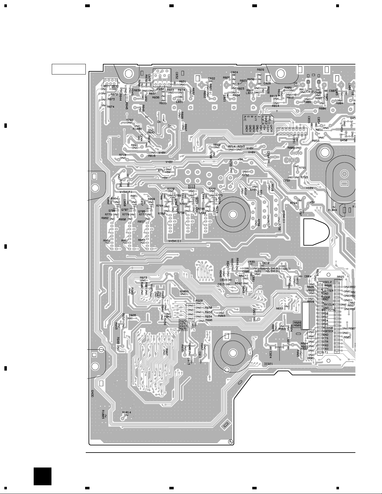
Q45Q450Q774Q771Q768Q706Q707Q708
IC921
(VNP1852-B)
SIDE B
DV-47A, DV-S733A, DV-747A
A
B
23
4
C
D
52
C
1234
Page 53
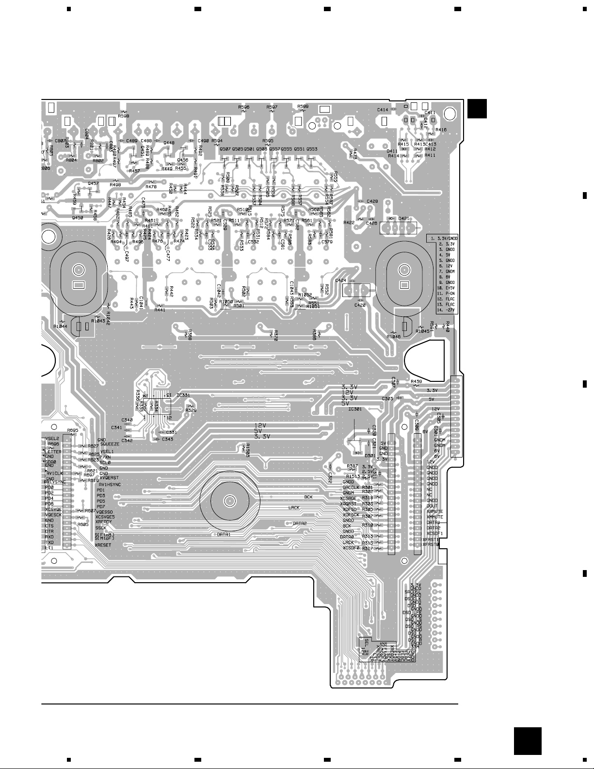
5
678
DV-47A, DV-S733A, DV-747A
C
AVJB
ASSY
A
B
C
D
Q457 Q451 Q448 Q456 Q507 Q505 Q501 Q503 Q557 Q555 Q551 Q553Q450
IC331 IC301
5
6
C
7
8
53
Page 54
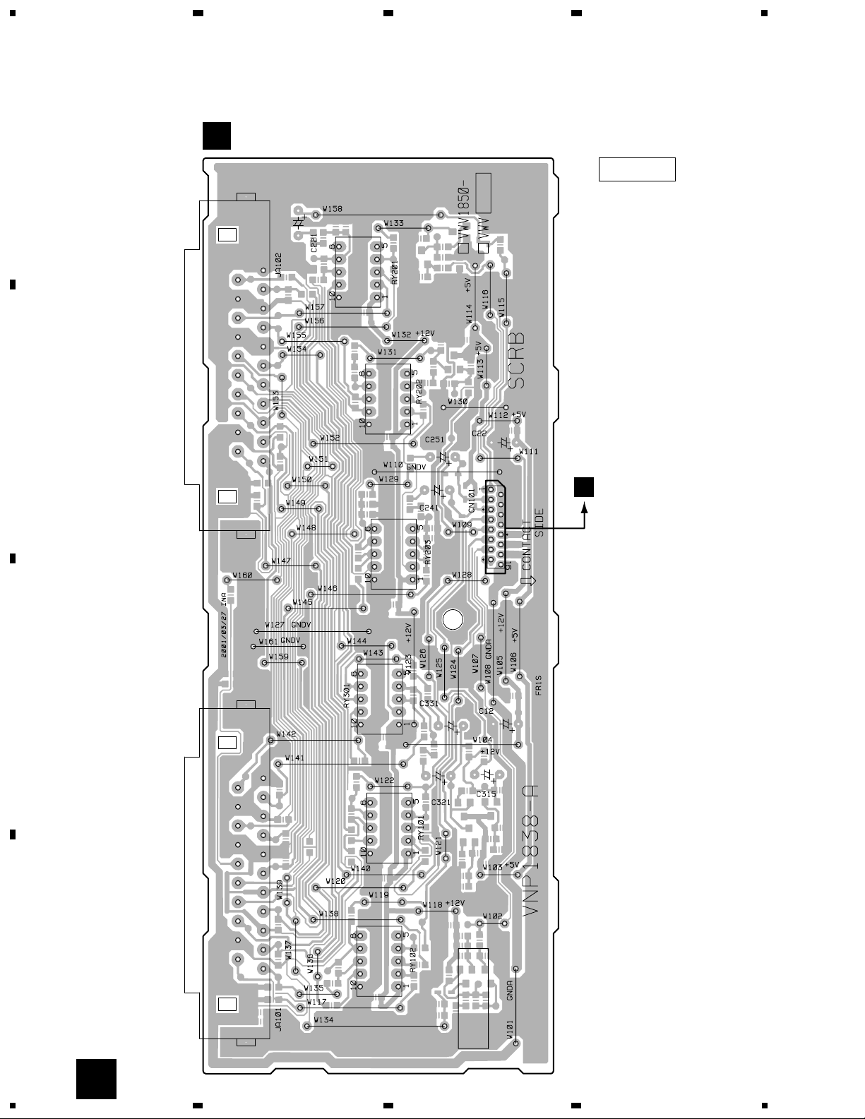
1
DV-47A, DV-S733A, DV-747A
4.4 SCRB ASSY (For WYXJ Type)
D
A
B
SCRB ASSY
23
SIDE A
4
CN702
C
C
D
54
D
1234
(VNP1838-A)
Page 55
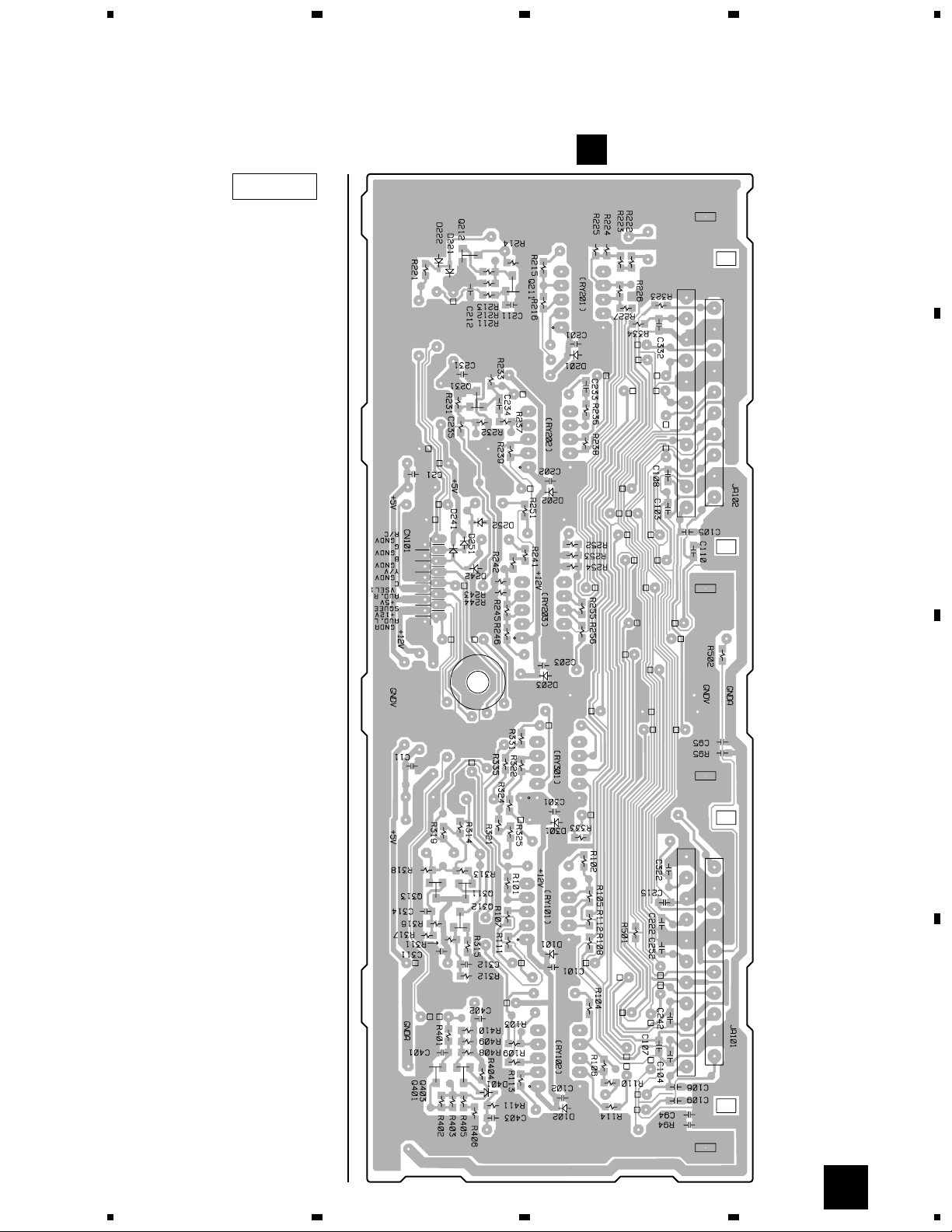
1
SIDE B
Q212
Q211
Q231
234
DV-47A, DV-S733A, DV-747A
D
SCRB ASSY
A
B
Q231
Q313 Q311
Q312
Q401 Q403
C
D
(VNP1838-A)
1
2
3
D
4
55
Page 56
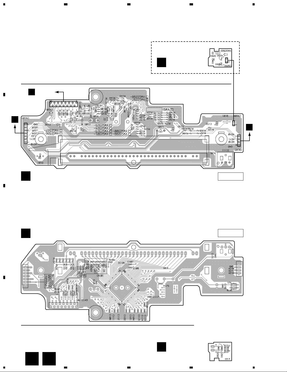
1
23
DV-47A, DV-S733A, DV-747A
4
4.5 FLIR, DILB ASSY
A
CN301
C
CN201
F
B
IC103
Except KUXJ/CA Type
I
DILB ASSY
Q101
IC111
CN251
G
E
FLIR ASSY
C
E
FLIR ASSY
SIDE A
(VNP1852-B)
SIDE B
D
56
E I
1234
IC101
I
DILB ASSY
Page 57
1
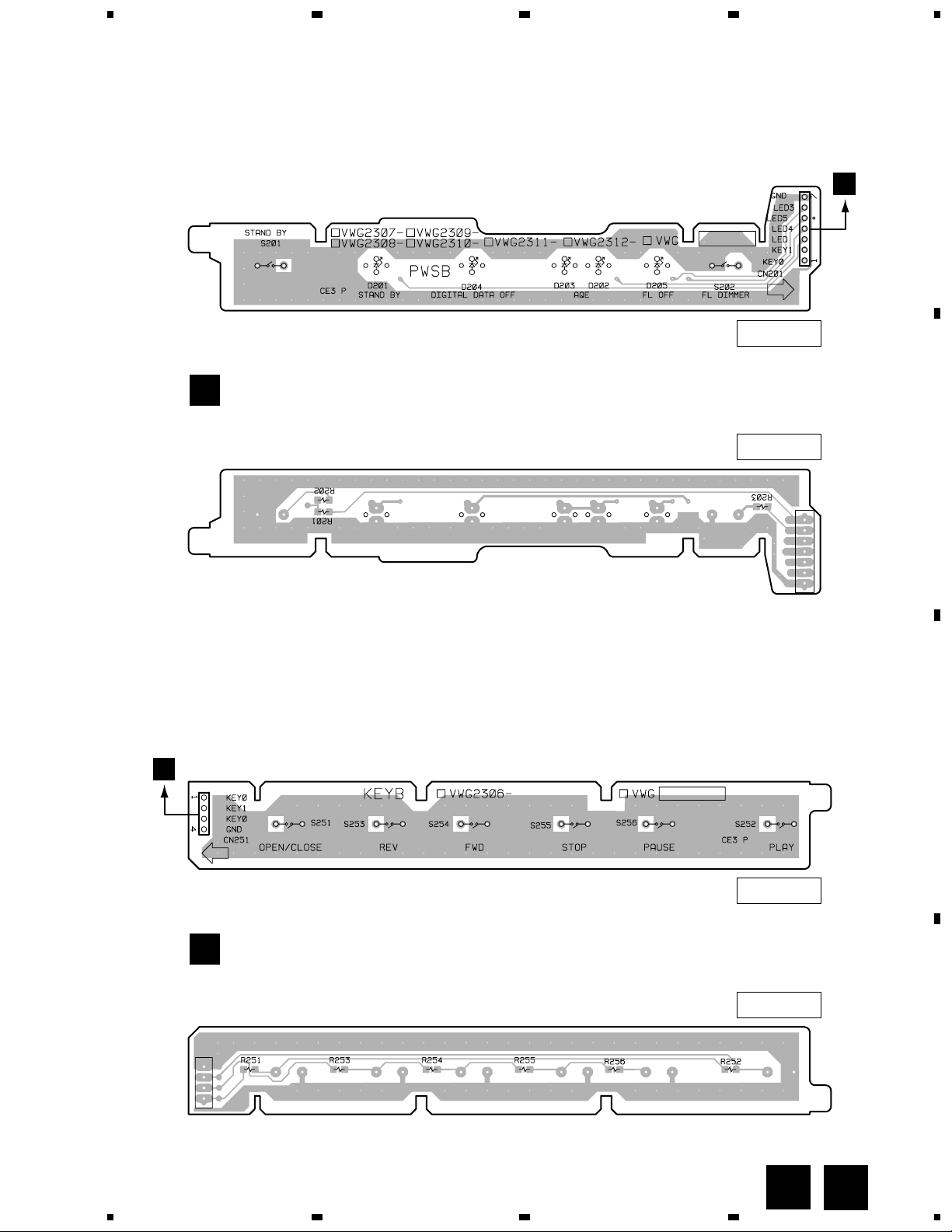
4.6 PWSB, KEYB ASSY
234
DV-47A, DV-S733A, DV-747A
F
PWSB ASSY
SIDE A
(VNP1852-B)
SIDE B
CN102
E
A
B
CN103
E
G
1
KEYB ASSY
C
SIDE A
(VNP1852-B)
SIDE B
D
F
2
3
G
4
57
Page 58
1
23
DV-47A, DV-S733A, DV-747A
4.7 POWER SUPPLY UNIT
4
A
(Short)
AC IN
H
POWER SUPPLY UNIT
B
Q001 IC001
IC104
C
IC103
C
Q105 Q104
IC102
D
IC101
CN303
SIDE A
58
H
1234
Page 59
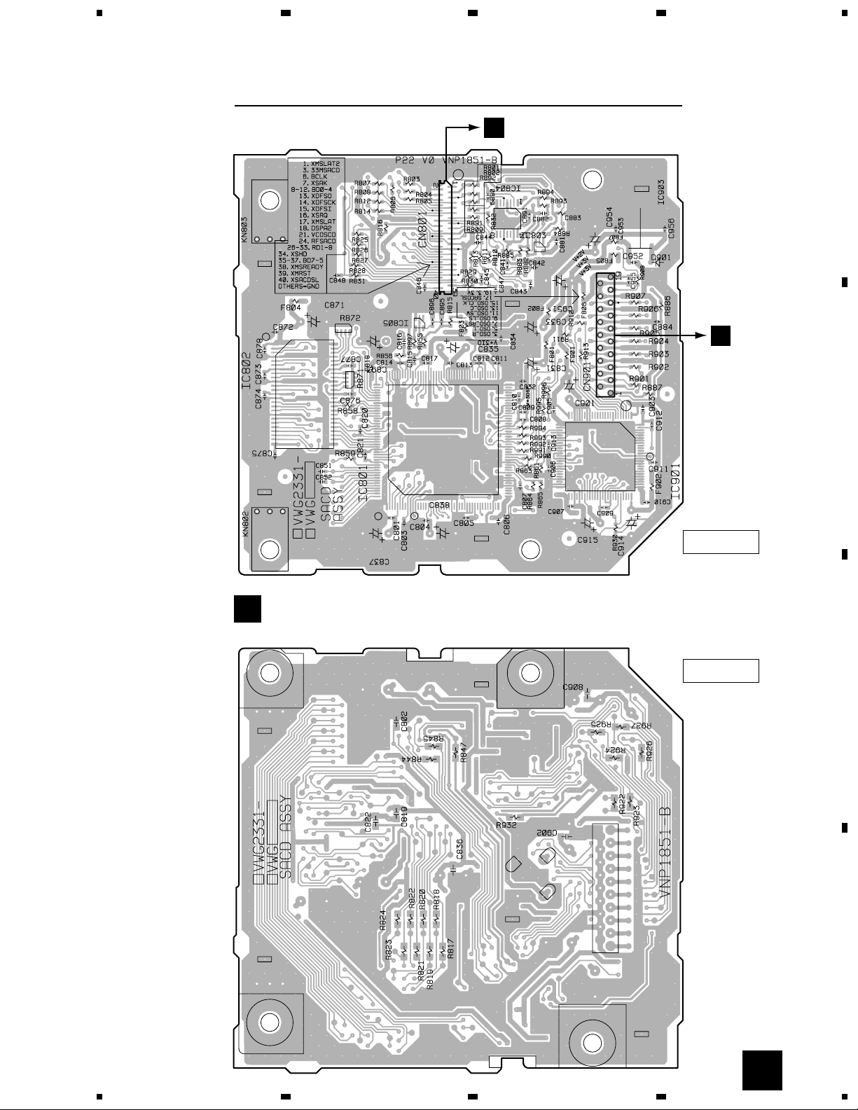
1
4.8 SACD ASSY
234
IC802 IC801 IC901IC805 IC804 IC903IC803
B
CN602
DV-47A, DV-S733A, DV-747A
C
CN304
A
B
J
SACD ASSY
SIDE A
(VNP1851-B)
SIDE B
C
D
J
1
2
3
4
59
Page 60
DV-47A, DV-S733A, DV-747A
Mark No. Description Part No.
Mark No. Description Part No.
5. PCB PARTS LIST
NOTES:•Parts marked by "NSP" are generally unavailable because they are not in our Master Spare Parts List.
The mark found on some component parts indicates the importance of the safety factor of the part.
•
Therefore, when replacing, be sure to use parts of identical designation.
When ordering resistors, first convert resistance values into code form as shown in the following examples.
•
Ex.1 When there are 2 effective digits (any digit apart from 0), such as 560 ohm and 47k ohm (tolerance is shown by J=5%,
and K=10%).
560 Ω→56 × 10
47k Ω→47 × 103→ 473 ........................................................ RD1/4PU 4 7 3 J
0.5 Ω→R50 ..................................................................................... RN2H
1 Ω→1R0 ..................................................................................... RS1P
Ex.2 When there are 3 effective digits (such as in high precision metal film resistors).
5.62k Ω→ 562 × 10
7 LIST OF WHOLE PCB ASSEMBLIES
Mark RemarksSymbol and Description
NSP
LOADING MECHANISM ASSY
NSP
LOAB ASSY
DVDM ASSY
NSP
FLJB ASSY
FLIR ASSY
NSP
KEYB ASSY
NSP
PWSB ASSY
AVJB ASSY
NSP
DILB ASSY
1
→ 561 ........................................................ RD1/4PU 5 6 1 J
R 5 0
1 R 0
1
→ 5621 ...................................................... RN1/4PC 5 6 2 1 F
Part No.
DV-47A
/KUXJ/CA
VWT1188
VWG2279
VWS1471
VWM2108
VWG2327
VWG2306
VWG2312
VWV1874
Not used
DV-S733A
/LBXJ
VWT1188
VWG2279
VWS1471
VWM2111
VWG2325
VWG2306
VWG2310
VWV1877
VWG2322
DV-S733A
/WLXJ/NC
VWT1188
VWG2279
VWS1471
VWM2109
VWG2324
VWG2306
VWG2310
VWV1875
VWG2322
DV-S733A
/WLXJ/RD
K
K
DV-747A
/WYXJ
VWT1188
VWG2279
VWS1471
VWM2110
VWG2326
VWG2306
VWG2311
VWV1876
VWG2322
NSP
SACD ASSY
SCRB ASSY
POWER SUPPLY UNIT
E
FLIR ASSY
VWG2331
Not used
VWR1346
VWG2331
Not used
VWR1346
VWG2331
Not used
VWR1346
VWG2327, VWG2325, VWG2324 and VWG2326 are constructed the same except for the following :
Mark Symbol and Description
Q101
R125
R126, R127
R129
R141
R142
CN104 CONNECTOR
VWG2327
Not used
Not used
Not used
RS1/16S0R0J
RS1/16S393J
RS1/16S104J
Not used
VWG2325
DTC124EK
RS1/16S0R0J
RS1/16S681J
Not used
RS1/16S153J
RS1/16S123J
S2B-PH-K-S
Part No.
VWG2324
DTC124EK
RS1/16S0R0J
RS1/16S681J
Not used
RS1/16S683J
RS1/16S273J
S2B-PH-K-S
VWG2331
VWV1850
VWR1346
VWG2326
DTC124EK
RS1/16S0R0J
RS1/16S681J
Not used
RS1/16S333J
RS1/16S473J
S2B-PH-K-S
Remarks
60
Page 61
DV-47A, DV-S733A, DV-747A
Mark No. Description Part No.
F
PWSB ASSY
Mark No. Description Part No.
VWG2312, VWG2310 and VWG2311 are constructed the same except for the following :
Mark Symbol and Description
D202
D203
D204, D205
S202
R203
VWG2312
SLR-56VC(NPQ)
Not used
Not used
ASG7013
RS1/16S0R0
Part No.
VWG2310
Not used
SLR-56DC(NPQ)
SLR-56VC(NPQ)
Not used
Not used
VWG2311
Not used
SLR-56DC(NPQ)
SLR-56VC(NPQ)
Not used
Not used
7 PCB PARTS LIST FOR DV-47A/KUXJ/CA UNLESS OTHERWISE NOTED
Mark No. Description Part No.
LOAB ASSY
SWITCHES AND RELAYS
S101 REAF SWITCH VSK1011
OTHERS
CN602 CONNECTOR S2B-PH-K
CN601 CONNECTOR S5B-PH-K
PRINTED CIRCUIT BOARD VNP1836
Mark No. Description Part No.
Q114, Q130 2SC4081
Q107, Q111, Q115, Q241, Q271 DTC114EUA
Q281 DTC114EUA
Q101, Q102, Q106 HN1A01F
Q103, Q141, Q142, Q542, Q543 HN1B04FU
Q112, Q113 HN1C01FU
Q108 HN1K03FU
Q571 RN1911
Q117, Q171, Q601 RN4982
D302, D303 KV1470
D601 RB501V-40
Remarks
DVDM ASSY
SEMICONDUCTORS
IC261, IC281, IC302 BA4510F
IC251 BA6664FM
IC481 BU2288FV
IC702
IC802 HY57V161610DTC-8
IC902 IS61LV6416-12T
IC903 IS63LV1024-12T
IC101 LA9701M
IC201 LC78652W
IC904 LC89051V
IC351 M56788AFP
IC804
IC801 M65774BFP
IC909 MM1561JF
IC601 PD6345A
IC701 PE5220A
IC111, IC271 TC74HC4053AFT
IC612 TC74VHC125FT
IC491 TC74VHC153FT
IC906, IC908 TC74VHC157FT
IC608 TC74VHCT125AFT
IC401, IC911–IC913 TC7SH04FU
IC532 TC7SH32FU
IC303, IC304, IC306 TC7SZU04F
IC907 TC7WH125FU
IC905 TC7WH157FU
IC211 TK15404M
IC603 VYW1896
IC901 XCA56367PV150
Q109, Q210 2SA1576A
GM71VS65803CLT-5
M5M4V18165DTP-6S
COILS AND FILTERS
L946 LCYA1R0J2520
L304 LCYA1R5J2520
L315, L418, L489, L893
L516–L523 CHIP BEADS VTL1083
L481 CHIP BEADS VTL1084
CAPACITORS
C480, C481, C516–C523, C662 CCSRCH100D50
C152 CCSRCH101J50
C104–C108, C314 CCSRCH150J50
C151 CCSRCH270J50
C324, C391, C392 CCSRCH331J50
C146 CCSRCH390J50
C122, C123 CCSRCH391J50
C116, C134, C283, C284, C297 CCSRCH470J50
C145, C241 CCSRCH560J50
C281, C282 CCSRCH5R0C50
C286 CCSRCH680J50
C117, C360 CCSRCH681J50
C124 CCSRCH820J50
C128, C142, C189, C201, C233 CEV101M16
C254, C358, C364, C368, C369 CEV101M16
C401, C407, C413, C944 CEV101M16
C113, C139 CEV220M16
C147, C219, C237, C326, C410 CEV221M4
C620, C701, C710, C803, C822 CEV221M4
C902, C992 CEV221M4
C111, C207 CEV470M6R3
C140, C223, C224, C264, C312 CKSQYB105K10
C209, C211, C216, C275, C313 CKSRYB102K50
C351 CKSRYB102K50
C133, C136, C203, C220, C225 CKSRYB103K50
CHIP BEADS
VTL1082
61
Page 62
DV-47A, DV-S733A, DV-747A
Mark No. Description Part No.
C234, C239, C261, C320–C322 CKSRYB103K50
C330, C591, C619, C705, C707 CKSRYB103K50
C943, C947 CKSRYB103K50
C101, C103, C118–C120 CKSRYB104K16
C212, C213, C227, C231 CKSRYB104K16
C248–C251, C255, C263, C315 CKSRYB104K16
C317 CKSRYB104K16
C208, C210 CKSRYB222K50
C271–C274 CKSRYB223K50
C266 CKSRYB224K10
C206, C214, C242, C357 CKSRYB472K50
C946 CKSRYB473K50
C102, C121, C138, C143, C154 CKSRYF104Z25
C256, C279, C285, C332, C353 CKSRYF104Z25
C359, C365, C366, C402 CKSRYF104Z25
C475–C477, C609, C768 CKSRYF104Z25
C772, C773 CKSRYF104Z25
C109, C114, C115, C125 CKSRYF105Z10
C130, C131, C144, C148, C150 CKSRYF105Z10
C160, C200, C202, C204, C215 CKSRYF105Z10
C217, C221, C222, C226, C230 CKSRYF105Z10
C232, C236, C253, C258, C265 CKSRYF105Z10
C298, C299, C310, C319 CKSRYF105Z10
C328, C329, C361, C393, C400 CKSRYF105Z10
C404, C406, C408, C411, C451 CKSRYF105Z10
C491, C532, C542, C543 CKSRYF105Z10
C602–C605, C607, C608, C610 CKSRYF105Z10
C613–C616, C618, C622, C626 CKSRYF105Z10
C628, C631, C657, C658 CKSRYF105Z10
C703, C704, C708, C715, C721 CKSRYF105Z10
C727, C730, C740, C743, C749 CKSRYF105Z10
C753, C757, C762, C774–C778 CKSRYF105Z10
C783, C796, C804, C807, C808 CKSRYF105Z10
C810, C812, C820, C821 CKSRYF105Z10
C823–C830, C835, C836, C838 CKSRYF105Z10
C841–C843, C847, C848, C856 CKSRYF105Z10
C859, C862, C863, C865, C867 CKSRYF105Z10
C873, C874, C877, C880 CKSRYF105Z10
C882, C883, C888, C894, C898 CKSRYF105Z10
C901, C903, C905–C908 CKSRYF105Z10
C911–C913, C918–C920 CKSRYF105Z10
C923–C926, C929, C933, C934 CKSRYF105Z10
C938, C942, C945, C948, C949 CKSRYF105Z10
C956, C957, C965, C974, C980 CKSRYF105Z10
C986, C988, C991, C993–C995 CKSRYF105Z10
C129, C149, C403 (100µF/6.3V) VCH1194
C205, C405, C452 (150µF/4V) VCH1195
C472, C601 (150µF/4V) VCH1195
C623, C700, C702 (150µF/4V) VCH1195
C801, C840 (150µF/4V) VCH1195
C904, C941, C996 (150µF/4V) VCH1195
C367 (33µF/16V) VCH1197
Mark No. Description Part No.
R123 RAB4C470J
R202, R341 RS1/10S101J
R126–R129, R176–R179 RS1/10S220J
R287 RS1/16S1002F
R364, R369, R373, R375 RS1/16S1003F
R289, R358, R361 RS1/16S1503F
R288 RS1/16S2201F
R357, R362, R363, R368, R372 RS1/16S6802F
R374 RS1/16S6802F
R257 (1.0Ω, 1/4W) VCN1127
R258, R259 (2.2Ω, 1/4W) VCN1128
Other Resistors RS1/16S&&&J
OTHERS
CN602 FFC CONNECTOR DKN1196
CN104 4P CONNECTOR DKN1223
CN103 CONNECTOR S5B-PH-SM3
FLEXIBLE CABLE VDA1681
CN101 FFC CONNECT0R VKN1787
CN401, CN501
CN105 12P CONNECTOR VKN1795
X481 (27.000MHz) VSS1159
X601 (16.5MHz) VSS1160
B TO B CONNECTOR 40P
VKN1788
AVJB ASSY (VWV1874 : KUXJ/CA)
SEMICONDUCTORS
IC601 ADV7300KST
IC301 BA25BC0FP
IC921 BA25BC0FP
IC441, IC501, IC551 CS4392D-KS
IC902 K4S643232E–TC60
IC701, IC702 LA7138M
IC442, IC502, IC552 NJM5532MD
IC422 NJM78M05FA
IC331 PD0274A
IC901 PM0033A
IC421 PQ15RW11
IC333, IC351, IC371 TC74VHC157FT
IC361, IC362 TC7SH32FU
IC332, IC334, IC352, IC353 TC7SHU04FU
Q442, Q446, Q502, Q506, Q552 2SA1037K
Q556, Q601–Q606, Q701–Q708 2SA1037K
Q421 2SC1740S
Q391 2SC2412K
Q444, Q448–Q452, Q456, Q457 2SD2114K
Q504, Q508, Q554, Q558 2SD2114K
Q441, Q443, Q445, Q447, Q501 DTC114YK
Q503, Q505, Q507, Q551, Q553 DTC114YK
Q555, Q557 DTC114YK
D411, D423 1SS355
RESISTORS
R800, R895 RAB4C0R0J
R543, R545, R631, R714, R744 RAB4C103J
R903, R931, R934, R940 RAB4C103J
R121, R757, R763, R790, R868 RAB4C220J
R873 RAB4C220J
62
COILS AND FILTERS
L702, L704, L706 LAU100J
L701, L703, L705 LAU4R7J
F721–F723 12MHz LPF(VIDEO) VTF1175
L1020, L300, L329 CHIP BEADS VTL1084
L368, L370 CHIP BEADS VTL1084
L386, L441, L473 CHIP BEADS VTL1084
L501, L551 CHIP BEADS VTL1084
L821, L822 CHIP BEADS VTL1089
Page 63

DV-47A, DV-S733A, DV-747A
Mark No. Description Part No.
CAPACITORS
C477, C497, C532, C533, C579 CCSRCH101J50
C581 CCSRCH101J50
C1053, C1054, C2041, C462, C465 CCSRCH102J50
C482, C485, C512, C515, C522 CCSRCH102J50
C525, C562, C565, C572, C575 CCSRCH102J50
C719, C749, C759 CCSRCH150J50
C463, C466, C483, C486, C513 CCSRCH221J50
C516, C523, C526, C563, C566 CCSRCH221J50
C573, C576 CCSRCH221J50
C720, C750, C760 CCSRCH270J50
C718, C748, C758 CCSRCH330J50
C412, C715, C716 CCSRCH470J50
C717, C741, C747, C751, C757 CCSRCH7R0D50
C761 CCSRCH7R0D50
C631 CCSRCH821J25
C312, C339 CEAL101M6R3
C710, C714, C746 CEAT100M50
C431, C511, C514, C521, C524 CEAT101M16
C561, C564, C571, C574 CEAT101M16
C700, C701, C736, C738, C793 CEAT101M16
C397, C603, C725, C752 CEAT101M6R3
C787, C789, C796, C798, C910 CEAT101M6R3
C912, C914, C918, C921, C923 CEAT101M6R3
C951 CEAT101M6R3
C821 CEAT102M6R3
Mark No. Description Part No.
RESISTORS
R961–R963 RAB4C103J
R971, R972, R975 RAB4C220J
R461, R475, R481, R495, R511 RN1/16SE1202D
R521, R532, R535, R561, R571 RN1/16SE1202D
R582, R585 RN1/16SE1202D
R464, R467, R484, R487, R514 RN1/16SE1502D
R517, R524, R527, R564, R567 RN1/16SE1502D
R574, R577 RN1/16SE1502D
R462, R465, R482, R485, R512 RN1/16SE2201D
R515, R522, R525, R562, R565 RN1/16SE2201D
R572, R575 RN1/16SE2201D
R474, R476, R494, R496, R531 RN1/16SE3301D
R533, R534, R536, R581 RN1/16SE3301D
R583, R584, R586 RN1/16SE3301D
R666, R667, R726–R728, R953 RS1/16S1201F
R655 RS1/16S1502F
R428 RS1/16S2201D
R952 RS1/16S3001F
R741, R751, R761 RS1/16S3300D
R668, R669, R954 RS1/16S3300F
R746, R748 RS1/16S3301F
R656 RS1/16S4702F
R672, R676, R680, R684, R688 RS1/16S5600F
R692 RS1/16S5600F
R747, R749 RS1/16S5601F
C394, C503, C553 CEAT1R0M50
C801, C802, C805, C806, C823 CEAT471M6R3
C825 CEAT471M6R3
C443 CEHAT1R0M50
C445, C505, C555 CEHAT220M50
C423, C427, C791, C795 CEHAZA101M16
C429, C452, C507, C557 CEHAZA221M16
C338, C356, C375, C601 CEHAZA221M6R3
C517, C527, C567 CEHAZA470M35
C577 CEHAZA470M35
C425, C442, C502, C552 CEHAZA471M6R3
C705, C740 CEHAZL331M16
C1041–C1043, C1048, C1049 CKSRYB103K50
C324–C326 CKSRYB103K50
C712, C733, C734, C809, C810 CKSRYB104K16
C632 CKSRYB392K50
C920 CKSRYF103Z50
C333, C351, C371, C382, C383 CKSRYF104Z25
C392, C396, C398, C411, C426 CKSRYF104Z25
C444, C447, C504, C508, C554 CKSRYF104Z25
C558, C602, C604–C614, C619 CKSRYF104Z25
C671–C673, C681–C683 CKSRYF104Z25
C702–C704, C706–C709, C737 CKSRYF104Z25
C739, C745, C788, C792, C794 CKSRYF104Z25
C797, C857, C860, C862, C871 CKSRYF104Z25
C922, C924 CKSRYF104Z25
C1044, C2042, C307, C320, C321 CKSRYF105Z10
C331, C332, C334, C335 CKSRYF105Z10
C352–C354, C372, C422, C424 CKSRYF105Z10
C428, C441, C475, C501, C529 CKSRYF105Z10
C551, C582, C911, C913, C919 CKSRYF105Z10
C925–C950, C952–C965 CKSRYF105Z10
C420, C421 CKSRYF224Z16
C461, C464, C481, C484 (100µF) VCH1192
C467, C487 (47µF) VCH1236
R801, R803, R805, R807, R809 RS1/16S62R0D
R811, R821, R823, R827 RS1/16S62R0D
R649–R654, R674, R678, R682 RS1/16S6800F
R427 RS1/16S6801D
R657 RS1/16S6801F
Other Resistors RS1/16S&&&J
OTHERS
CN303 CONNECTOR 14P 14P-FJ
CN301 15P CONNECTOR 15P-1.25FJ
CN403 JACK AKN1006
JA702 SOCKET AKP7116
JA402 OPT. LINK OUT GP1FA502TZ
PCB BINDER VEF1040
JA701 JACK VKB1123
JA502 JACK VKB1125
JA501 JACK VKB1129
JA703 JACK VKB1151
JA401 JACK VKB1160
CN703 7P CONNECTOR VKN1267
CN304 19P CONNECTOR VKN1775
CN302, CN601
SHIELDING PLATE VNF1124
B TO B CONNECTOR 40P
AVJB ASSY (VWV1877 : LBXJ)
SEMICONDUCTORS
IC601 ADV7300KST
IC301 BA25BC0FP
IC921 BA25BC0FP
IC441, IC501, IC551 CS4392D-KS
IC902 K4S643232E–TC60
VKN1789
63
Page 64

DV-47A, DV-S733A, DV-747A
Mark No. Description Part No.
IC701, IC702 LA7138M
IC442, IC502, IC552 NJM5532MD
IC422 NJM78M05FA
IC331 PD0274A
IC901 PM0033A
IC421 PQ15RW11
IC333, IC351, IC371 TC74VHC157FT
IC1503, IC361, IC362 TC7SH32FU
IC1502 TC7SH86FU
IC332, IC334, IC352, IC353 TC7SHU04FU
IC1505 TC7WH157FU
IC1501 TC7WH74FU
Q442, Q446, Q502, Q506, Q552 2SA1037K
Q556, Q601–Q606, Q701–Q708 2SA1037K
Q421 2SC1740S
Q391 2SC2412K
Q444, Q448–Q452, Q456, Q457 2SD2114K
Q504, Q508, Q554, Q558 2SD2114K
Q1001, Q1002, Q441, Q443, Q445 DTC114YK
Q447, Q501, Q503, Q505, Q507 DTC114YK
Q551, Q553, Q555, Q557 DTC114YK
D411, D423 1SS355
COILS AND FILTERS
L702, L704, L706 LAU100J
L701, L703, L705 LAU4R7J
L901 LCYA1R0J2520
F721–F723 12MHz LPF(VIDEO) VTF1175
L1020, L1512 CHIP BEADS VTL1084
L1531–L1533, L300 CHIP BEADS VTL1084
L329, L368, L370 CHIP BEADS VTL1084
L386, L441 CHIP BEADS VTL1084
L473, L501, L551 CHIP BEADS VTL1084
L821, L822, L831, L832
CHIP BEADS
VTL1089
CAPACITORS
C463, C466, C483, C486, C513 CCSRCH101J50
C516, C523, C526, C563, C566 CCSRCH101J50
C573, C576 CCSRCH101J50
C462, C465, C482, C485, C512 CCSRCH102J50
C515, C522, C525, C562, C565 CCSRCH102J50
C572, C575 CCSRCH102J50
C719, C749, C759 CCSRCH150J50
C741, C751, C761 CCSRCH180J50
C720, C750, C760 CCSRCH270J50
C718, C748, C758 CCSRCH330J50
C412, C715, C716 CCSRCH470J50
C717, C747, C757 CCSRCH7R0D50
C631 CCSRCH821J25
C477, C497, C532, C533, C579 CCSRCH821J50
C581 CCSRCH821J50
C312, C339 CEAL101M6R3
C306, C310 CEAL470M16
C710, C714, C746 CEAT100M50
C431, C511, C514, C521, C524 CEAT101M16
C561, C564, C571, C574 CEAT101M16
C700, C701, C736, C738, C793 CEAT101M16
C397, C603, C725, C752, C787 CEAT101M6R3
C789, C796, C798, C910, C912 CEAT101M6R3
C914, C918, C921, C923, C951 CEAT101M6R3
C821, C831 CEAT102M6R3
Mark No. Description Part No.
C394 CEAT1R0M50
C801, C802, C805, C806, C823 CEAT471M6R3
C825, C833, C835 CEAT471M6R3
C443, C503, C553 CEHAT1R0M50
C445, C505, C555 CEHAT220M50
C423, C427, C791, C795 CEHAZA101M16
C429, C452, C507, C557 CEHAZA221M16
C338, C356, C375, C601 CEHAZA221M6R3
C517, C527, C567, C577 CEHAZA470M35
C425, C442, C502, C552 CEHAZA471M6R3
C705, C740 CEHAZL331M16
C1055, C324–C326 CKSRYB103K50
C1041–C1043, C1501, C712 CKSRYB104K16
C733, C734, C809, C810 CKSRYB104K16
C632 CKSRYB392K50
C920 CKSRYF103Z50
C1505, C333, C351, C371 CKSRYF104Z25
C382, C383, C392, C396, C398 CKSRYF104Z25
C411, C426, C444, C447, C504 CKSRYF104Z25
C508, C554, C558, C602, C604 CKSRYF104Z25
C608, C610, C611, C671–C673 CKSRYF104Z25
C681–C683, C702–C704 CKSRYF104Z25
C706–C709, C737, C739, C745 CKSRYF104Z25
C788, C792, C794, C797, C857 CKSRYF104Z25
C860, C862, C871, C922, C924 CKSRYF104Z25
C1048, C1049, C1440, C1502–C1504CKSRYF105Z10
C1506, C1591, C2042, C301, C303 CKSRYF105Z10
C305, C307, C320, C321 CKSRYF105Z10
C331, C332, C334, C335 CKSRYF105Z10
C352–C354, C372, C422, C424 CKSRYF105Z10
C428, C441, C451, C475, C501 CKSRYF105Z10
C506, C529, C551, C556, C582 CKSRYF105Z10
C605–C607, C609, C612–C614 CKSRYF105Z10
C619, C911, C913, C919 CKSRYF105Z10
C925–C950, C952–C965 CKSRYF105Z10
C309, C420, C421 CKSRYF224Z16
C461, C464, C481, C484 (100µF) VCH1192
C467, C487 (47µF) VCH1236
RESISTORS
R961–R963 RAB4C103J
R971, R972, R975 RAB4C220J
R461, R475, R481, R495, R511 RN1/16SE1202D
R521, R532, R535, R561, R571 RN1/16SE1202D
R582, R585 RN1/16SE1202D
R464, R467, R484, R487, R514 RN1/16SE1502D
R517, R524, R527, R564, R567 RN1/16SE1502D
R574, R577 RN1/16SE1502D
R462, R465, R482, R485, R512 RN1/16SE2201D
R515, R522, R525, R562, R565 RN1/16SE2201D
R572, R575 RN1/16SE2201D
R474, R476, R494, R496, R531 RN1/16SE3301D
R533, R534, R536, R581 RN1/16SE3301D
R583, R584, R586 RN1/16SE3301D
R667 RS1/16S1001F
R726–R728, R953 RS1/16S1201F
R666 RS1/16S1501F
R428 RS1/16S2201D
R952 RS1/16S3001F
R741, R751, R761 RS1/16S3300D
64
Page 65
DV-47A, DV-S733A, DV-747A
Mark No. Description Part No.
R954 RS1/16S3300F
R652–R654, R672, R676, R680 RS1/16S4700F
R669, R684, R688, R692 RS1/16S5600F
R801, R803, R805, R807, R809 RS1/16S62R0D
R811, R821, R823, R827, R831 RS1/16S62R0D
R833, R837 RS1/16S62R0D
R649–R651, R674, R678, R682 RS1/16S6800F
R427 RS1/16S6801D
R655, R657 RS1/16S6801F
Other Resistors RS1/16S&&&J
OTHERS
CN303 CONNECTOR 14P 14P-FJ
CN301 15P CONNECTOR 15P-1.25FJ
CN403 JACK AKN1006
JA702 SOCKET AKP7116
CN704 D-SOCKET(14P) AKP7170
JA402 OPT. LINK OUT GP1FA502TZ
PCB BINDER VEF1040
JA701 JACK VKB1123
JA502 JACK VKB1125
JA501 JACK VKB1129
JA703 JACK VKB1151
JA401 JACK VKB1160
CN703 7P CONNECTOR VKN1267
CN304 19P CONNECTOR VKN1775
CN302, CN601
SHIELDING PLATE VNF1124
B TO B CONNECTOR 40P
VKN1789
AVJB ASSY
(VWV1875 : WLXJ/NC, WLXJ/RD)
SEMICONDUCTORS
IC601 ADV7300KST
IC301 BA25BC0FP
IC921 BA25BC0FP
IC441, IC501, IC551 CS4392D-KS
IC902 K4S643232E-TC60
IC701, IC702 LA7138M
IC442, IC502, IC552 NJM5532MD
IC422 NJM78M05FA
IC331 PD0274A
IC901 PM0033A
IC421 PQ15RW11
IC333, IC351, IC371 TC74VHC157FT
IC1503, IC361, IC362 TC7SH32FU
IC1502 TC7SH86FU
IC332, IC334, IC352, IC353 TC7SHU04FU
IC1505 TC7WH157FU
IC1501 TC7WH74FU
Q442, Q446, Q502, Q506, Q552 2SA1037K
Q556, Q601–Q606, Q701–Q708 2SA1037K
Q421 2SC1740S
Q391 2SC2412K
Q444, Q448–Q452, Q456, Q457 2SD2114K
Q504, Q508, Q554, Q558 2SD2114K
Q1001, Q1002, Q441, Q443, Q445 DTC114YK
Q447, Q501, Q503, Q505, Q507 DTC114YK
Q551, Q553, Q555, Q557 DTC114YK
D411, D423 1SS355
Mark No. Description Part No.
COILS AND FILTERS
L702, L704, L706 LAU100J
L701, L703, L705 LAU4R7J
L901 LCYA1R0J2520
F721–F723 12MHz LPF(VIDEO) VTF1175
L1020, L1512 CHIP BEADS VTL1084
L1531–L1533, L300 CHIP BEADS VTL1084
L329, L368, L370 CHIP BEADS VTL1084
L386, L441 CHIP BEADS VTL1084
L473, L501, L551 CHIP BEADS VTL1084
L821, L822, L831, L832
CHIP BEADS
VTL1089
CAPACITORS
C463, C466, C483, C486, C513 CCSRCH101J50
C516, C523, C526, C563, C566 CCSRCH101J50
C573, C576 CCSRCH101J50
C462, C465, C482, C485, C512 CCSRCH102J50
C515, C522, C525, C562, C565 CCSRCH102J50
C572, C575 CCSRCH102J50
C719, C749, C759 CCSRCH150J50
C741, C751, C761 CCSRCH180J50
C720, C750, C760 CCSRCH270J50
C718, C748, C758 CCSRCH330J50
C412, C715, C716 CCSRCH470J50
C717, C747, C757 CCSRCH7R0D50
C631 CCSRCH821J25
C477, C497, C532, C533, C579 CCSRCH821J50
C581 CCSRCH821J50
C312, C339 CEAL101M6R3
C306, C310 CEAL470M16
C710, C714, C746 CEAT100M50
C431, C511, C514, C521, C524 CEAT101M16
C561, C564, C571, C574 CEAT101M16
C700, C701, C736, C738, C793 CEAT101M16
C397, C603, C725, C752, C787 CEAT101M6R3
C789, C796, C798, C910, C912 CEAT101M6R3
C914, C918, C921, C923, C951 CEAT101M6R3
C821, C831 CEAT102M6R3
C394 CEAT1R0M50
C801, C802, C805, C806, C823 CEAT471M6R3
C825, C833, C835 CEAT471M6R3
C443, C503, C553 CEHAT1R0M50
C445, C505, C555 CEHAT220M50
C423, C427, C791, C795 CEHAZA101M16
C429, C452, C507, C557 CEHAZA221M16
C338, C356, C375, C601 CEHAZA221M6R3
C517, C527, C567, C577 CEHAZA470M35
C425, C442, C502, C552 CEHAZA471M6R3
C705, C740 CEHAZL331M16
C1055, C324–C326 CKSRYB103K50
C1041–C1043, C1501, C712 CKSRYB104K16
C733, C734, C809, C810 CKSRYB104K16
C632 CKSRYB392K50
C920 CKSRYF103Z50
C1505, C333, C351, C371 CKSRYF104Z25
C382, C383, C392, C396, C398 CKSRYF104Z25
C411, C426, C444, C447, C504 CKSRYF104Z25
C508, C554, C558, C602, C604 CKSRYF104Z25
C608, C610, C611, C671–C673 CKSRYF104Z25
C681–C683, C702–C704 CKSRYF104Z25
C706–C709, C737, C739, C745 CKSRYF104Z25
C788, C792, C794, C797, C857 CKSRYF104Z25
C860, C862, C871, C922, C924 CKSRYF104Z25
65
Page 66
DV-47A, DV-S733A, DV-747A
Mark No. Description Part No.
C1048, C1049, C1440, C1502–C1504CKSRYF105Z10
C1506, C1591, C2042, C301, C303 CKSRYF105Z10
C305, C307, C320, C321 CKSRYF105Z10
C331, C332, C334, C335 CKSRYF105Z10
C352–C354, C372, C422, C424 CKSRYF105Z10
C428, C441, C451, C475, C501 CKSRYF105Z10
C506, C529, C551, C556, C582 CKSRYF105Z10
C605–C607, C609, C612–C614 CKSRYF105Z10
C619, C911, C913, C919 CKSRYF105Z10
C925–C950, C952–C965 CKSRYF105Z10
C309, C420, C421 CKSRYF224Z16
C461, C464, C481, C484 (100µF) VCH1192
C467, C487 (47µF) VCH1236
RESISTORS
R961–R963 RAB4C103J
R971, R972, R975 RAB4C220J
R461, R475, R481, R495, R511 RN1/16SE1202D
R521, R532, R535, R561, R571 RN1/16SE1202D
R582, R585 RN1/16SE1202D
R464, R467, R484, R487, R514 RN1/16SE1502D
R517, R524, R527, R564, R567 RN1/16SE1502D
R574, R577 RN1/16SE1502D
R462, R465, R482, R485, R512 RN1/16SE2201D
R515, R522, R525, R562, R565 RN1/16SE2201D
R572, R575 RN1/16SE2201D
R474, R476, R494, R496, R531 RN1/16SE3301D
R533, R534, R536, R581 RN1/16SE3301D
R583, R584, R586 RN1/16SE3301D
R667 RS1/16S1001F
R726–R728, R953 RS1/16S1201F
R666 RS1/16S1501F
R428 RS1/16S2201D
R952 RS1/16S3001F
R741, R751, R761 RS1/16S3300D
R954 RS1/16S3300F
R652–R654, R672, R676, R680 RS1/16S4700F
R669, R684, R688, R692 RS1/16S5600F
R801, R803, R805, R807, R809 RS1/16S62R0D
R811, R821, R823, R827, R831 RS1/16S62R0D
R833, R837 RS1/16S62R0D
R649–R651, R674, R678, R682 RS1/16S6800F
R427 RS1/16S6801D
R655, R657 RS1/16S6801F
Other Resistors RS1/16S&&&J
OTHERS
CN303 CONNECTOR 14P 14P-FJ
CN301 15P CONNECTOR 15P-1.25FJ
CN403 JACK AKN1006
JA702 SOCKET AKP7116
CN704 D-SOCKET(14P) AKP7170
JA402 OPT. LINK OUT GP1FA502TZ
PCB BINDER VEF1040
JA701 JACK VKB1123
JA502 JACK VKB1125
JA501 JACK VKB1129
JA703 JACK VKB1151
JA401 JACK VKB1160
CN703 7P CONNECTOR VKN1267
CN304 19P CONNECTOR VKN1775
CN302, CN601
B TO B CONNECTOR 40P
VKN1789
Mark No. Description Part No.
AVJB ASSY (VWV1876 : WYXJ)
SEMICONDUCTORS
IC601 ADV7300KST
IC301 BA25BC0FP
IC921 BA25BC0FP
IC441, IC501, IC551 CS4392D-KS
IC902 K4S643232E-TC60
IC701, IC702 LA7138M
IC708 MM1506XN
IC710 MM1508XN
IC706, IC707 MM1509XN
IC442, IC502, IC552 NJM5532MD
IC422 NJM78M05FA
IC331 PD0274A
IC901 PM0033A
IC421 PQ15RW11
IC333, IC351, IC371 TC74VHC157FT
IC1503, IC361, IC362 TC7SH32FU
IC1502 TC7SH86FU
IC332, IC334, IC352, IC353 TC7SHU04FU
IC1505 TC7WH157FU
IC1501 TC7WH74FU
Q442, Q446, Q502, Q506, Q552 2SA1037K
Q556, Q601–Q606, Q701–Q708 2SA1037K
Q768, Q771, Q774, Q981–Q983 2SA1037K
Q421 2SC1740S
Q391 2SC2412K
Q444, Q448–Q452, Q456, Q457 2SD2114K
Q504, Q508, Q554, Q558 2SD2114K
Q441, Q443, Q445, Q447, Q501 DTC114YK
Q503, Q505, Q507, Q551, Q553 DTC114YK
Q555, Q557 DTC114YK
D411, D423, D721–D728 1SS355
COILS AND FILTERS
L702, L704, L706 LAU100J
L701, L703, L705 LAU4R7J
L901 LCYA1R0J2520
F706–F708 6MHz LPF(VIDEO) VTF1174
F721–F723 12MHz LPF(VIDEO) VTF1175
L1020, L1512 CHIP BEADS VTL1084
L1531–L1533, L300 CHIP BEADS VTL1084
L329, L368, L370 CHIP BEADS VTL1084
L386, L441 CHIP BEADS VTL1084
L473, L501, L551 CHIP BEADS VTL1084
L821, L822 CHIP BEADS VTL1089
CAPACITORS
C463, C466, C483, C486, C513 CCSRCH101J50
C516, C523, C526, C563, C566 CCSRCH101J50
C573, C576 CCSRCH101J50
C462, C465, C482, C485, C512 CCSRCH102J50
C515, C522, C525, C562, C565 CCSRCH102J50
C572, C575 CCSRCH102J50
C719, C749, C759 CCSRCH150J50
C741, C751, C761 CCSRCH180J50
C720, C750, C760 CCSRCH270J50
C718, C748, C758 CCSRCH330J50
66
SHIELDING PLATE VNF1124
Page 67

DV-47A, DV-S733A, DV-747A
Mark No. Description Part No.
C412, C715, C716 CCSRCH470J50
C717, C747, C757 CCSRCH7R0D50
C631 CCSRCH821J25
C477, C497, C532, C533, C579 CCSRCH821J50
C581 CCSRCH821J50
C312, C339 CEAL101M6R3
C306, C310 CEAL470M16
C710, C714, C722, C746, C753 CEAT100M50
C762 CEAT100M50
C431, C511, C514, C521, C524 CEAT101M16
C561, C564, C571, C574 CEAT101M16
C700, C701, C736, C738, C793 CEAT101M16
C397, C603, C725, C752, C787 CEAT101M6R3
C789, C796, C798, C910, C912 CEAT101M6R3
C914, C918, C921, C923, C951 CEAT101M6R3
C821 CEAT102M6R3
C394 CEAT1R0M50
C801, C802, C805, C806, C823 CEAT471M6R3
C825 CEAT471M6R3
C443, C503, C553 CEHAT1R0M50
C445, C505, C555 CEHAT220M50
C423, C427, C791, C795 CEHAZA101M16
C429, C452, C507, C557 CEHAZA221M16
C338, C356, C375, C601 CEHAZA221M6R3
C517, C527, C567, C577 CEHAZA470M35
C425, C442, C502, C552 CEHAZA471M6R3
C705, C740 CEHAZL331M16
C1055, C324–C326 CKSRYB103K50
C1041–C1043, C1501, C712, C721 CKSRYB104K16
C733, C734, C780, C781 CKSRYB104K16
C809, C810 CKSRYB104K16
C632 CKSRYB392K50
C920 CKSRYF103Z50
C1505, C333, C351, C371 CKSRYF104Z25
C382, C383, C392, C396, C398 CKSRYF104Z25
C411, C426, C444, C447, C504 CKSRYF104Z25
C508, C554, C558, C602, C604 CKSRYF104Z25
C608, C610, C611, C671–C673 CKSRYF104Z25
C681–C683, C702–C704 CKSRYF104Z25
C706–C709, C723, C737, C739 CKSRYF104Z25
C745, C754, C763, C768, C771 CKSRYF104Z25
C774, C788, C790, C792, C794 CKSRYF104Z25
C797, C851, C852, C857, C860 CKSRYF104Z25
C862, C871, C922, C924 CKSRYF104Z25
C981–C983 CKSRYF104Z25
C1048, C1049, C1440, C1502–C1504CKSRYF105Z10
C1506, C1591, C2042, C301, C303 CKSRYF105Z10
C305, C307, C320, C321 CKSRYF105Z10
C331, C332, C334, C335 CKSRYF105Z10
C352–C354, C372, C422, C424 CKSRYF105Z10
C428, C441, C451, C475, C501 CKSRYF105Z10
C506, C529, C551, C556, C582 CKSRYF105Z10
C605–C607, C609, C612–C614 CKSRYF105Z10
C619, C911, C913, C919 CKSRYF105Z10
C925–C950, C952–C965 CKSRYF105Z10
C309, C420, C421 CKSRYF224Z16
C461, C464, C481, C484 (100µF) VCH1192
C467, C487 (47µF) VCH1236
Mark No. Description Part No.
RESISTORS
R961–R963 RAB4C103J
R971, R972, R975 RAB4C220J
R461, R475, R481, R495, R511 RN1/16SE1202D
R521, R532, R535, R561, R571 RN1/16SE1202D
R582, R585 RN1/16SE1202D
R464, R467, R484, R487, R514 RN1/16SE1502D
R517, R524, R527, R564, R567 RN1/16SE1502D
R574, R577 RN1/16SE1502D
R462, R465, R482, R485, R512 RN1/16SE2201D
R515, R522, R525, R562, R565 RN1/16SE2201D
R572, R575 RN1/16SE2201D
R474, R476, R494, R496, R531 RN1/16SE3301D
R533, R534, R536, R581 RN1/16SE3301D
R583, R584, R586 RN1/16SE3301D
R668 RS1/16S1000F
R667 RS1/16S1001F
R726–R728 RS1/16S1201F
R666 RS1/16S1501F
R428 RS1/16S2201D
R953 RS1/16S2201F
R719, R736, R738 RS1/16S3000D
R741, R751, R761 RS1/16S3300D
R954 RS1/16S3300F
R746, R748 RS1/16S3301F
R982, R986, R990 RS1/16S3900F
R952 RS1/16S5101F
R669, R672, R676, R680, R684 RS1/16S5600F
R688, R692 RS1/16S5600F
R747, R749 RS1/16S5601F
R801, R803, R805, R807, R809 RS1/16S62R0D
R811, R821, R823, R827 RS1/16S62R0D
R649–R654, R674, R678, R682 RS1/16S6800F
R427 RS1/16S6801D
R655, R657 RS1/16S6801F
R949–R951 RS1/16S68R0F
Other Resistors RS1/16S&&&J
OTHERS
CN303 CONNECTOR 14P 14P-FJ
CN301 15P CONNECTOR 15P-1.25FJ
CN403 JACK AKN1006
JA702 SOCKET AKP7116
JA402 OPT. LINK OUT GP1FA502TZ
PCB BINDER VEF1040
JA701 JACK VKB1123
JA502 JACK VKB1125
JA501 JACK VKB1129
JA703 JACK VKB1151
JA401 JACK VKB1160
CN702 16P CONNECTOR VKN1247
CN703 7P CONNECTOR VKN1267
CN304 19P CONNECTOR VKN1775
CN302, CN601
SHIELDING PLATE VNF1124
B TO B CONNECTOR 40P
VKN1789
67
Page 68
DV-47A, DV-S733A, DV-747A
Mark No. Description Part No.
SCRB ASSY (WYXJ ONLY)
SEMICONDUCTORS
Q212 2SA1037K
Q211, Q311–Q313, Q401, Q403 2SC2412K
D301, D401 1SS355
SWITCHES AND RELAYS
RY101, RY102, RY201 VSR1016
RY203, RY301 VSR1016
CAPACITORS
C103–C110 CCSRCH391J50
C221, C241, C251, C315 CEAT101M10
C321, C331 CEAT471M10
C101, C102, C11, C201, C203 CKSRYF104Z25
C21, C212, C215, C301 CKSRYF104Z25
C311, C312, C314, C402, C403 CKSRYF104Z25
C94 CKSRYF104Z25
RESISTORS
R215, R223, R242, R252, R321 RS1/16S68R0F
R331 RS1/16S68R0F
Other Resistors RS1/16S&&&J
OTHERS
JA101, JA102 CONNECTOR VKB1157
CN101 16P CONNECTOR VKN1247
PRINTED CIRCUIT BOARD VNP1838
Mark No. Description Part No.
PWSB ASSY
SEMICONDUCTORS
D202 SLR-56VC(NPQ)
SWITCHES AND RELAYS
S201, S202 ASG7013
RESISTORS
All Resistors RS1/16S&&&J
OTHERS
CN201 CONNECTOR 7P 07P-FJ
KEYB ASSY
SWITCHES AND RELAYS
S251–S256 ASG7013
RESISTORS
All Resistors RS1/16S &&&J
OTHERS
CN251 CONNECTOR 4P 04P-FJ
FLIR ASSY
SEMICONDUCTORS
IC101 PE5251A
IC103 PST3242
IC111 TSOP1840XG1
COILS AND FILTERS
L101 LAU680J
CAPACITORS
C111, C112, C121, C122 CCSRCH102J50
C132 CEAL101M6R3
C105, C142, C152 CEAL470M16
C102, C103 CKSRYF104Z25
C107 CKSRYF104Z50
C101, C104, C106, C108 CKSRYF105Z10
C131, C141 CKSRYF105Z10
C143, C151 CKSRYF224Z16
RESISTORS
All Resistors RS1/16S &&&J
OTHERS
CN103 CONNECTOR 4P 04R-FJ
CN102 CONNECTOR 7P 07R-FJ
CN101 15P CONNECTOR 15R-1.25FJ
V101 FL TUBE VAW1065
FL HOLDER VNK4748
POWER SUPPLY UNIT
OTHERS
P101 PROTECTOR(1.6A) AEK7066
F001 FUSE 1.25A REK1099
DILB ASSY (Except KUXJ/CA)
SEMICONDUCTORS
D291 NSPB500-0008
D292 UDZS6.2B
CAPACITORS
C291 CKSRYF105Z10
RESISTORS
All Resistors RS1/16S &&&J
OTHERS
CN291 CONNECTOR POST B2B-PH-K
68
X101 (5MHz) VSS1142
Page 69

DV-47A, DV-S733A, DV-747A
Mark No. Description Part No.
SACD ASSY
SEMICONDUCTORS
IC903 BA25BC0FP
IC801 CXD2753R
IC802 HY57V161610DTC-8
IC804 TC74VHC74FT
IC803 TC7SH08FU
COILS AND FILTERS
L801–L805, L807 CHIP BEADS VTL1082
CAPACITORS
C847, C882, C895 CCSRCH100D50
C837, C838, C871, C893, C954 CEHAZA101M16
C831, C833, C835, C951 CEHAZA221M6R3
C815, C816 CKSRYB103K50
C801, C804–C814, C817, C818 CKSRYF105Z10
C820, C821, C832, C834 CKSRYF105Z10
C872–C878, C881, C891 CKSRYF105Z10
C952, C953, C955, C956 CKSRYF105Z10
RESISTORS
R871, R872 RAB4C103J
Other Resistors RS1/16S&&&J
Mark No. Description Part No.
OTHERS
CN901 19P CONNECTOR 19R-1.25FJ
PCB BINDER VEF1040
CN801 FFC CONNECT0R VKN1794
69
Page 70
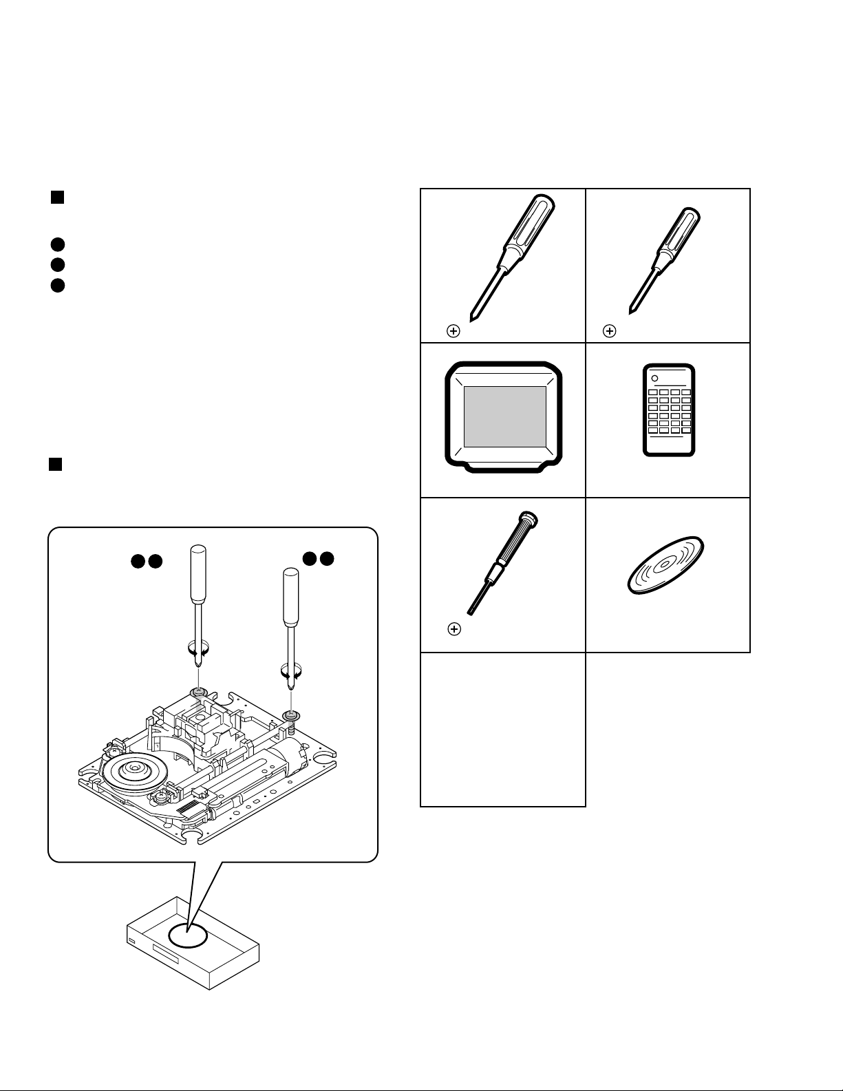
DV-47A, DV-S733A, DV-747A
6. ADJUSTMENT
6.1 ADJUSTMENT ITEMS AND
LOCATION
Adjustment Items
[Mechanism Part]
1
Tangential and Radial Height Coarse Adjustment
2
DVD Jitter Adjustment
3
Initialize the Focus Sweep Setting
[Electrical Part]
Electrical adjustments are not required.
Adjustment Points (Mechanism Part)
Cautions: After adjustment, adjustment screw locks with the
Screw tight.
6.2 JIGS AND MEASURING
INSTRUMENTS
Screwdriver (large)
TV monitor
Screwdriver (medium)
Test mode remote control
unit (GGF1067)
1 2
Tangential
adjustment
screw
1 2
Radial
adjustment
screw
Precise screwdriver
Screw tight
(GYL1001)
DVD test disc
(GGV1025)
70
Page 71
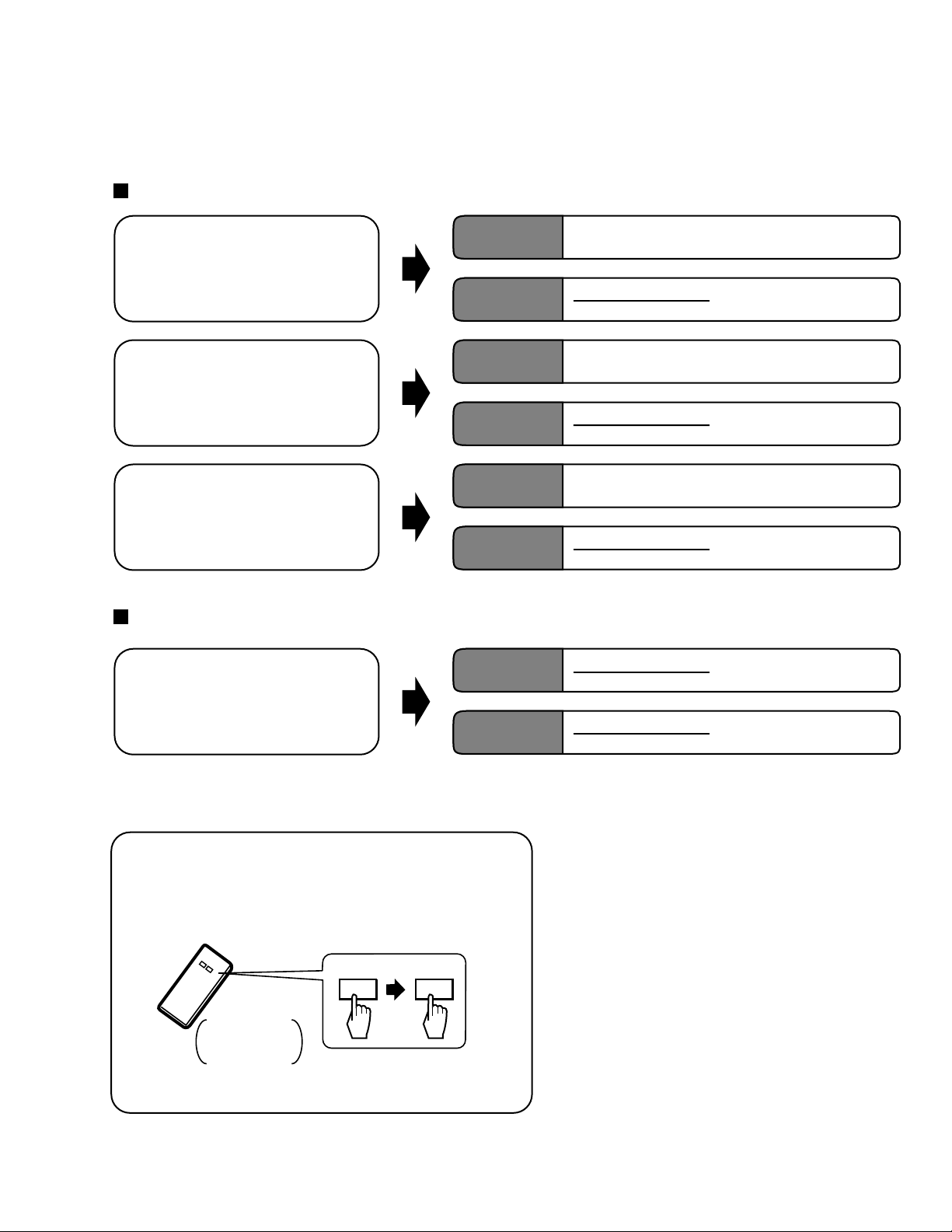
6.3 NECESSARY ADJUSTMENT POINTS
When Adjustment Points
Exchange Parts of Mechanism Assy
DV-47A, DV-S733A, DV-747A
Exchange the Pickup
Exchange the Traverse Mechanism
Exchange the Spindle Motor
Exchange PCB Assy
Exchange PC Board
Mechanical
point
Electric
point
Mechanical
point
Electric
point
Mechanical
point
Electric
point
Mechanical
point
~, Ÿ, !
!
Ÿ, !
∗ After adjustment, screw locks
with the Screw tight.
∗ After adjustment, screw locks
with the Screw tight.
LOAB, DVDM ASSY
∗
Purpose: To set the sweep which was correct with the
individual Traverse mechanism.
Be sure to perform the following step finally when replaced
Pickup, Traverse Mechanism and Spindle Motor.
ESC CLEAR
GGF1067
Test mode
remote control
unit
(It is necessary when performed adjustment procedure Ÿ.)
Electric
point
71
Page 72
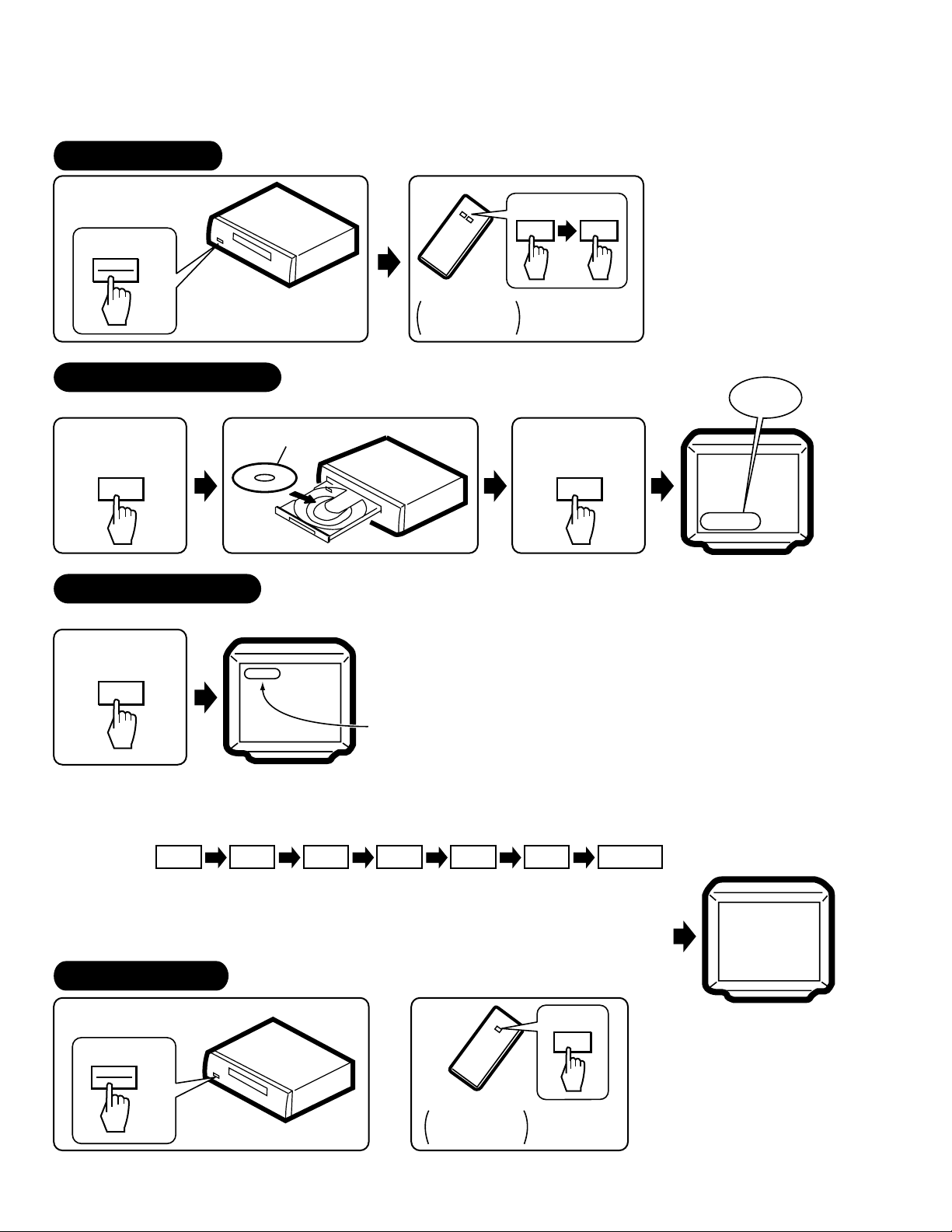
DV-47A, DV-S733A, DV-747A
6.4 TEST MODE
TEST MODE: ON
POWER
ON
ESC TEST
GGF1067
Test mode
remote control
unit
TEST MODE: DISC SET
<TRAY OPEN>
OPEN/CLOSE
(Player or Remote
Control Unit)
DVD disc
TEST MODE: PLAY
<PLAY>
TV/LDP
An address is displayed
< When playback with the target address of disc (DVD)>
For example, when playback with # 30000
OPEN/CLOSE
(Player or Remote
Control Unit)
DSC -
CHECK
DVD, CD
&&&
During PLAY
+10 3 0 0 0 0 CHP/TIM
TEST MODE: OFF
POWER
OFF
72
Press keys in order
030000
ESC
OR
GGF1067
Test mode
remote control
unit
Page 73
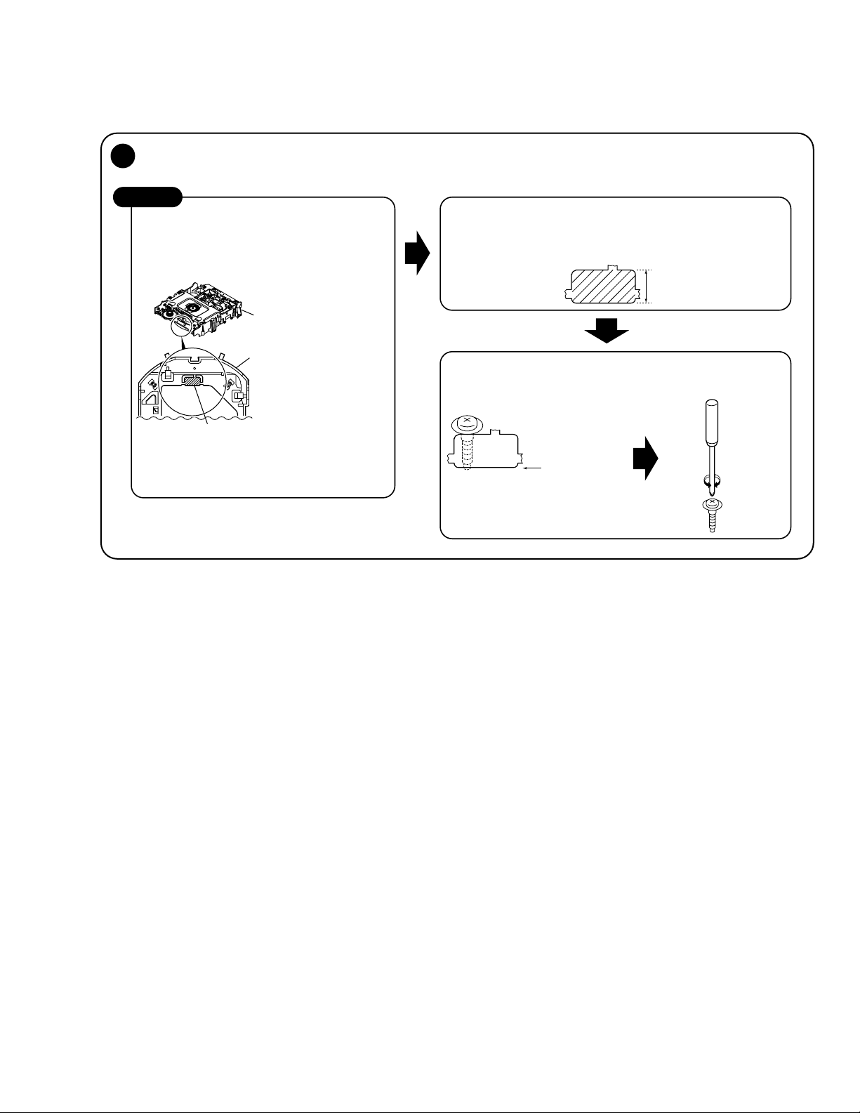
6.5 MECHANISM ADJUSTMENT
Tangential and Radial Height Coarse Adjustment
1
DV-47A, DV-S733A, DV-747A
START
• Remove the servo mechanism.
• Remove a Spacer for height adjustment
attached to the back side (shaded area)
of the Servo Mechanism (Float Base) with
nippers.
Servo Mechanism
Float Base
Spacer for Height adjustment
Note:
Turn the Short switch to Short side when
removing the Pickup Flexible Cable.
(Refer to "7.1.7 DISASSEBLY".)
Cautions:
Because there is not a Spacer for height adjustment in
adjustment after the second time, will keep it at need.
(This parts is Traverse mechanism exclusive use of a model
for 2001 years)
7.3mm
Put a spacer between a Tangential (or Radial) adjustment
screw and Mechanism Base and turn each screw to adjust
the height. (Refer to "6.1 ADJUSTMENT ITEMS AND
LOCATION".)
Turn a flat side
into bottom
73
Page 74
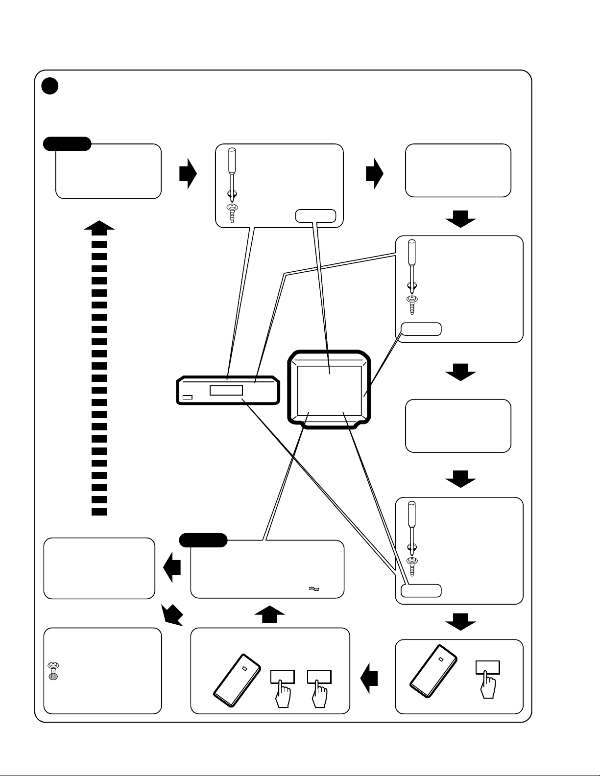
DV-47A, DV-S733A, DV-747A
DVD Jitter Adjustment
2
• Playback method of inner and outer address for the purpose is refererd to "6.4 TEST MODE".
• Jitter indication of the monitor is refererd to "7.1.4 TEST MODE SCREEN DISPLAY".
START
• Test mode
• Play the DVD test disc
at outer track
(around #200000)
Mechanism Assy
Adjust the Tangential
Adjustment Screw so that
jitter becomes minimum.
J4 : Min
Use disc: GGV1025
• Play the DVD test disc
at inner track
(around #30000)
Mechanism Assy
Adjust the Radial
Adjustment Screw so that
jitter becomes minimum.
J4 : Min
Turn the POWER OFF in
case of NG once, and
perform the adjustment
once again.
If error rate is OK,
locks a root of
tangential and radial
adjustment screws with
the Screw tight, and
go to step
!
.
CHECK
NG
OK
J4 : - - - -
Player
Monitor
Confirm the error rate that is
displayed "OK"
(Example ER (av): 2.5e - 5-*OK )
Disc playback normally.
• The measurement of block error rate
5ESC
• Play the DVD test disc
at outer track
(around #200000)
Mechanism Assy
Readjust the Tangential
Adjustment Screw so that
jitter becomes minimum.
J4 : Min
ESC
Screw tight: GYL1001
74
Test mode end
Page 75
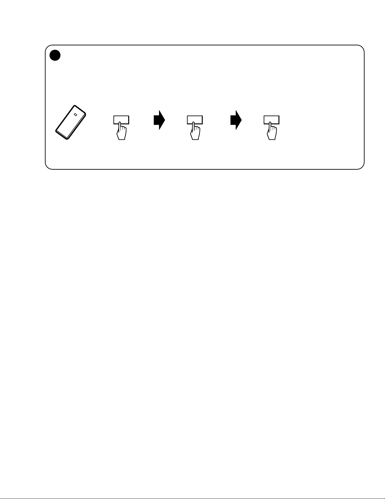
DV-47A, DV-S733A, DV-747A
Initialize the Focus Sweep Setting
3
Purpose: To set the sweep which was correct with the individual Traverse mechanism.
Turn on the Player
ESC CLEARPOWER
Note: Be sure to perform this step when replaced the Pickup or Traverse mechanism.
75
Page 76
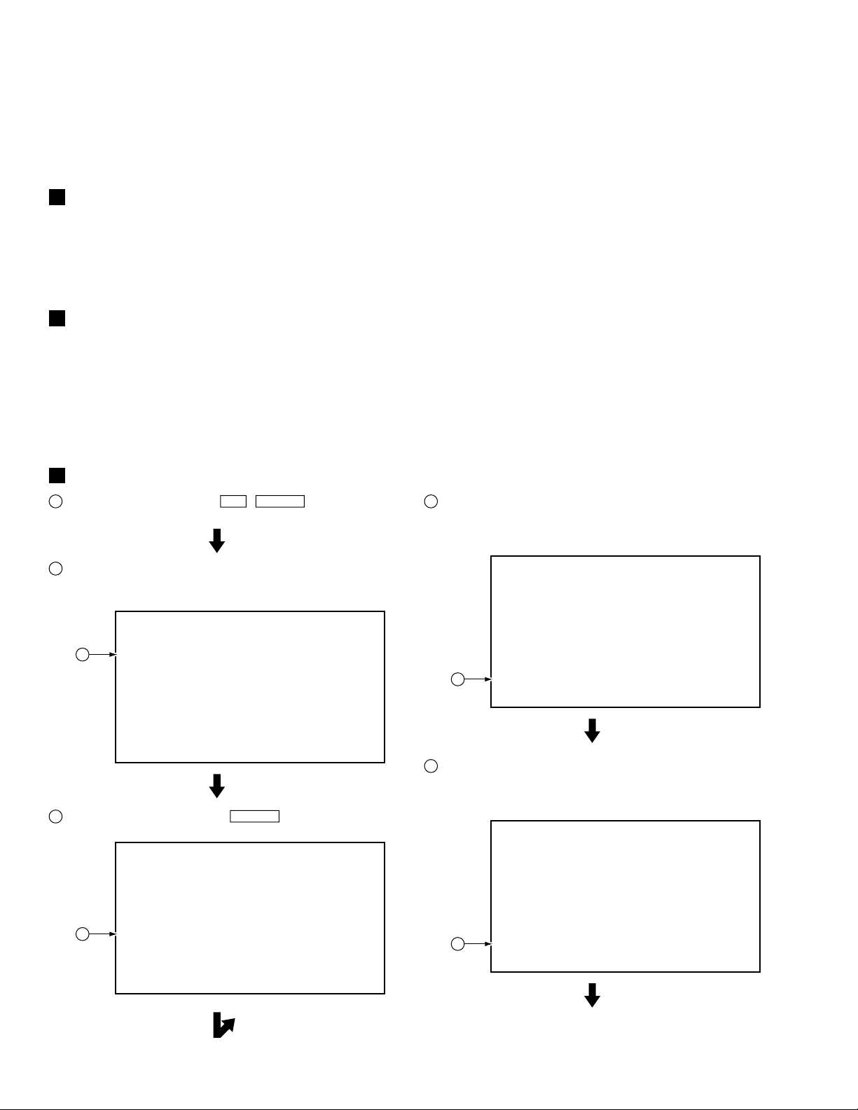
DV-47A, DV-S733A, DV-747A
7. GENERAL INFORMATION
7.1 DIAGNOSIS
7.1.1 ID NUMBER AND ID DATA SETTING
Entering the ID Number and ID Data for Players with DVD-Audio Compatibility
It is necessary with a player with DVD-audio compatibility to set an individual number (ID number) and ID data. If the number and data are
not set correctly with the following procedure, operations in the future may not be guaranteed. You will find the ID number to be set on the
yellow label on the rear panel.
Important: If no yellow label is found on the rear panel, write down the specified ID number by checking it according to "How to
confirm the ID number" shown below.
The Input is Necessary When:
• Downloading FLASH-ROM is finished. (The latest version must be downloaded when a repair is made.)
• "No ID Number" is displayed on the screen or FL display immediately after the power is turned on or in Stop mode.
• If "No ID DATA" is displayed, the ID data must be entered.
Note:
Be sure to enter the ID number in Stop mode.
Use the service remote control (GGF1067) for operations. Only opening/closing of the tray are performed from the player.
How to Input the ID Number and ID Data
1
To enter the input mode, press ESC + STEREO in a status with
no ID number set, such as after FLASH-ROM downloading.
2
As number input is enabled when the unit enters the input
mode, input the 9-digit ID number.
(The entered number is also displayed on the FL display.)
[Player's ID Number Setting]
ID Number ?
> - - - - - - - - -
2
<CLEAR> Exit
Input ID Number !
3
After inputting the number, press SEARCH to register the ID
number.
[Player's ID Number Setting]
ID Number ?
> 0 0 0 0 0 0 0 0 1 OK ?
4
When the ID number has been registered, the unit enters the ID
data input mode. (The FL display indicates "NO ID DATA.")
In this condition, place the ID data disc on the tray and close the
tray using the CLOSE key "7/0" on the player.
[Player's ID Data Setting]
<CLEAR> Exit
4
Insert The ID Data Disc !
5
While the data are being read, the message shown in the figure
at left is displayed on the screen.
(The FL display indicates "RD ID DATA.")
[Player's ID Data Setting]
76
<PLAY> Compare Mode
<SEARCH> Enter
3
Input ID Number !
5
Loading The ID Data Disc !
Page 77
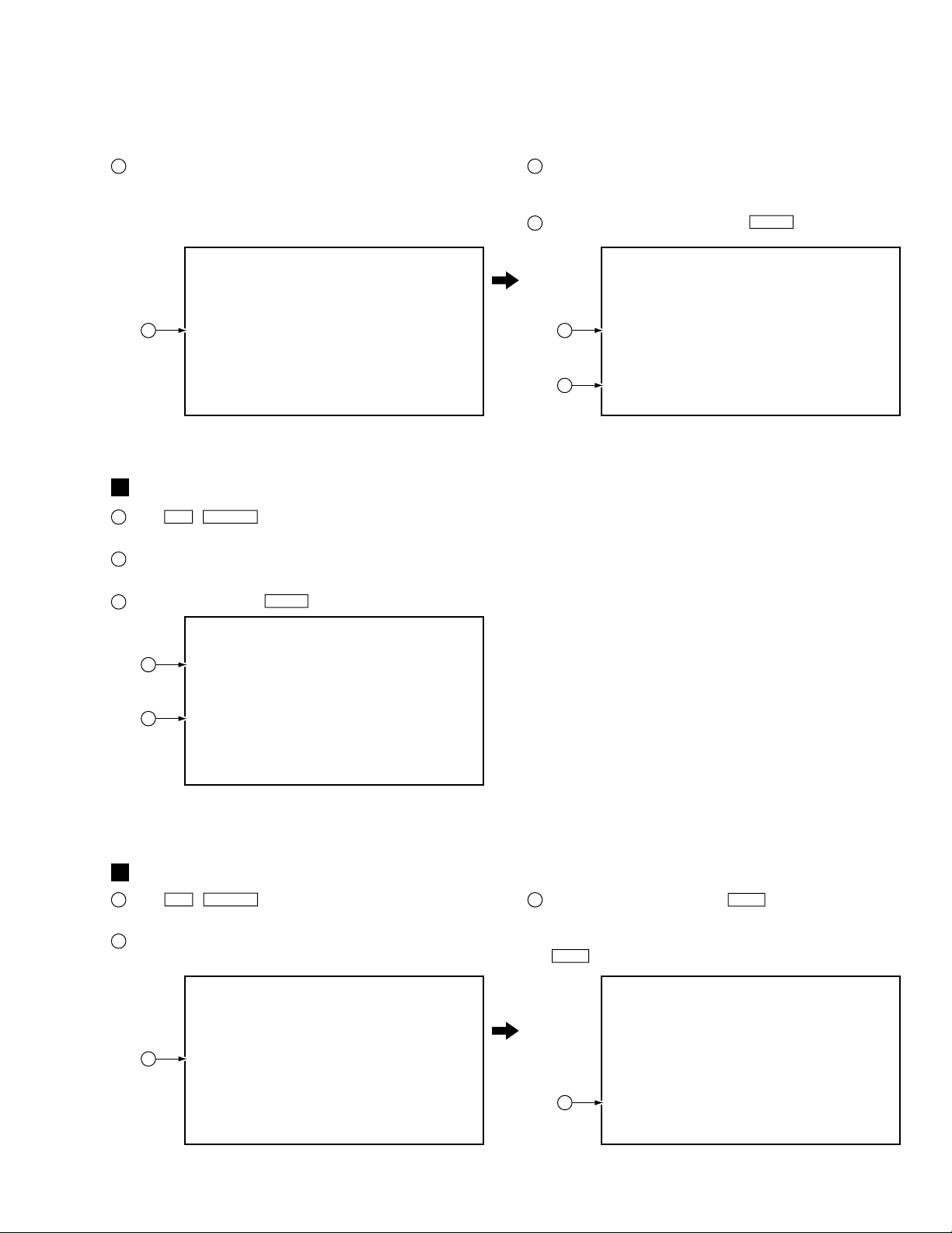
DV-47A, DV-S733A, DV-747A
6
When the ID data have been read, the data are written to the
FLASH-ROM.
(The FL display indicates "WR ID DATA.")
[Player's ID Data Setting]
Wait Rom Writing !
6
How to Confirm the ID Number
1
Press ESC + STEREO with an ID number set, and the unit
enters the ID number confirmation mode.
2
The set ID number is displayed on the screen (and on the FL
display), permitting you to confirm it.
To exit this mode, press CLEAR .
3
[Player's ID Number Setting]
ID Number ?
[ 0 0 0 0 0 0 0 0 1]
2
Compare
> * * * * * * * * *
<CLEAR> Exit
3
7
When the ID data have been written to the FLASH-ROM, the
message "Rom Write OK" is displayed on the screen.
(The FL display indicates "ID DATA OK.")
After confirming this message, press CLEAR to exit the input
8
mode.
[Player's ID Data Setting]
Rom Write OK !
7
<CLEAR> Exit
8
Input ID Number !
How to Clear the ID Number
1
Press ESC + STEREO with an ID number set, and the unit
enters the ID number confirmation mode.
2
Input the same number as the ID number you have set.
[Player's ID Number Setting]
ID Number ?
[ 0 0 0 0 0 0 0 0 1]
Compare
2
> * * * * * * * * *
<CLEAR> Exit
Input ID Number !
3
After inputting the number, press STOP .
Only when the entered number matches the set ID number, the
ID number is cleared and the unit exits this mode.
If the numbers do not match, you must return to step 2.
( STOP is not accepted until 9 digits are entered.)
[Player's ID Number Setting]
ID Number ?
[ 0 0 0 0 0 0 0 0 1]
Compare
> 0 0 0 0 0 0 0 0 1 OK ?
<PLAY> Enter
3
<STOP> Memory Clear
Input ID Number !
77
Page 78
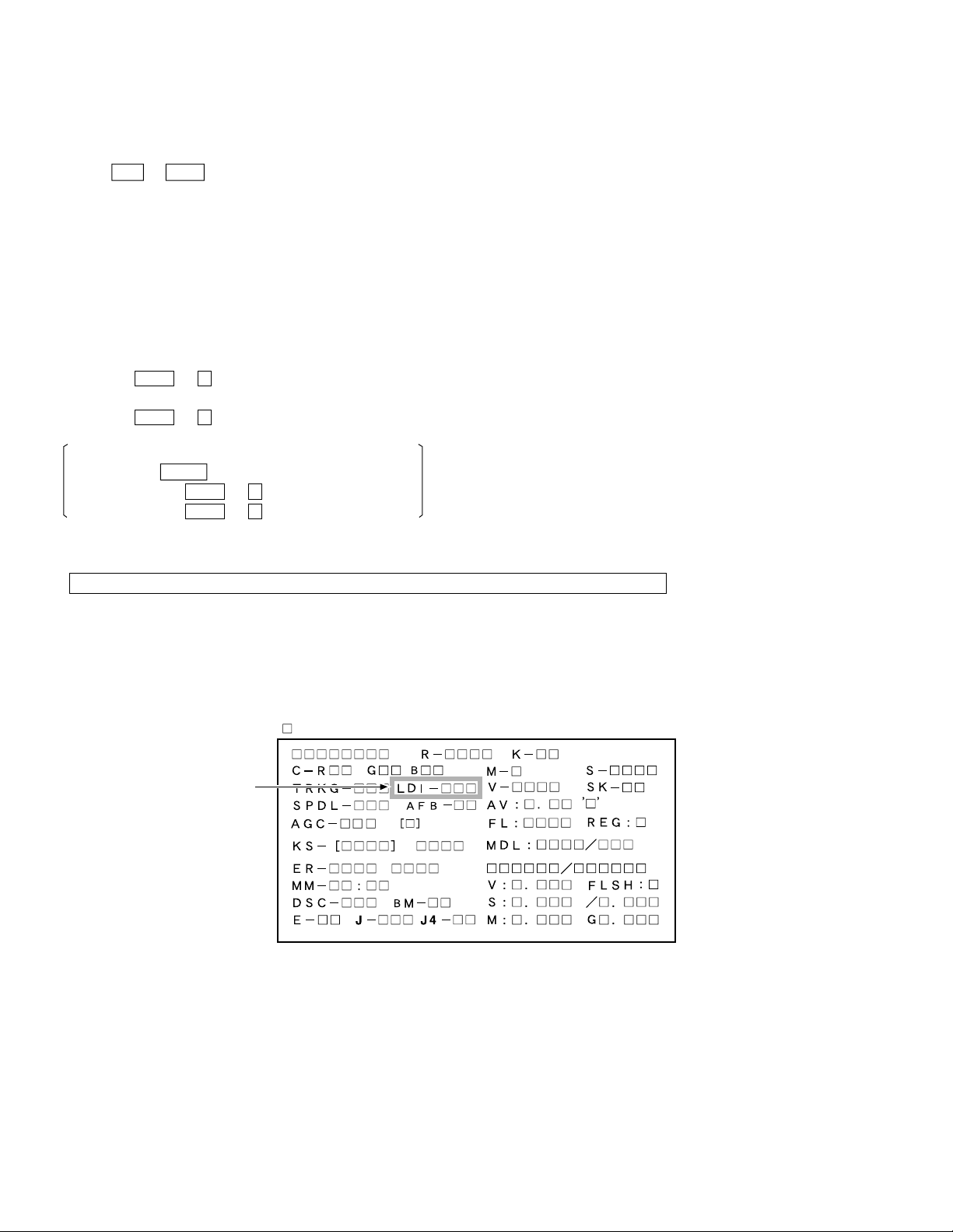
DV-47A, DV-S733A, DV-747A
7.1.2 SELF-DIAGNOSTIC FUNCTION OF PICKUP DEFECTIVE
This unit can confirm the laser diode current value (DVD: 650nm, CD: 780nm) of pickup on the Test Mode screen.
(Press the ESC → TEST keys in order on the test mode remote control unit (GGF1067) to enter the test mode.)
It's effective in case of the following condition.
Symptom
• Indicates "No Disc" in FL display.
• Player does not playback, etc..
Procedure of Self-Diagnosis
1 Enter the Test mode.
2 When diagnosing the 650nm laser diode:
Press the → keys in order, and turn on the laser diode (It light-up for nine seconds.).
When diagnosing the 780nm laser diode:
Press the → keys in order, and turn on the laser diode (It light-up for nine seconds.).
When let it turn on once again after performed 2 once,
After pressed REP.B key once
650nm: Press the → keys in order
780nm: Press the → keys in order
TEST 1
TEST 4
TEST 1
TEST 4
3 Confirm the indicated value of the laser diode current (LDI). (Refer to following figure.)
4 When indicated value is more than 100, pickup is defective. → Replacement is necessary
Replace the Traverse Mechanism Assy or Pickup.
Note :
When a DVD disc or a CD disc is played in the test mode, this function is effective.
Character in bold : Item name
: Information display
Laser diode current value
Test Mode Screen Display
78
Page 79
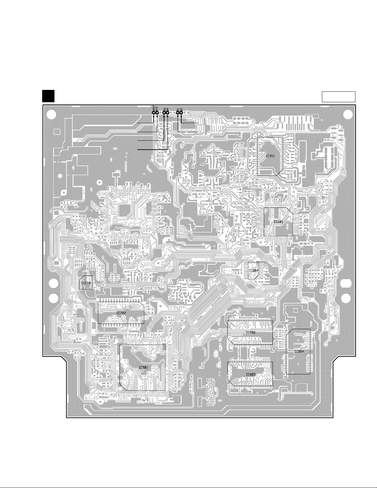
DVDM ASSY
B
SIDE A
Vref
RFO
B2
B1
B3
B4
This model has not test terminal.
Please use following points on the DVDM Assy when checking RF, FE and TE, etc..
7.1.3 TEST POINTS LOCATION
DV-47A, DV-S733A, DV-747A
79
Page 80
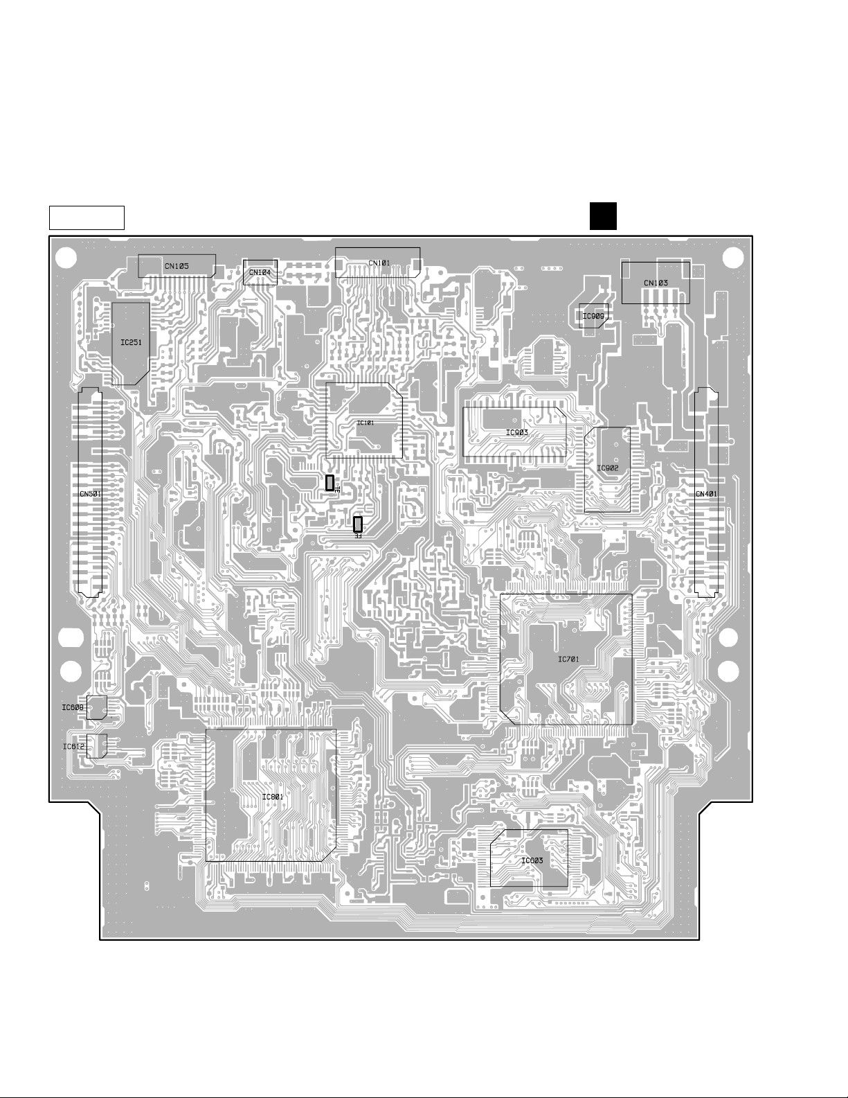
DV-47A, DV-S733A, DV-747A
SIDE B
TE
FE
B
DVDM ASSY
80
Page 81
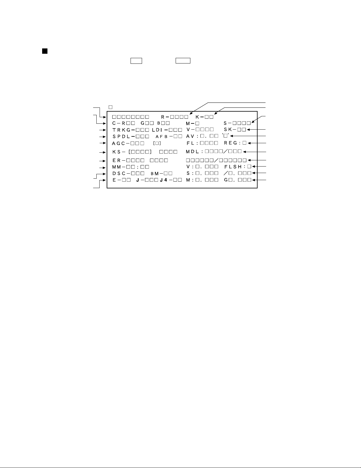
DV-47A, DV-S733A, DV-747A
7.1.4 TEST MODE SCREEN DISPLAY
TEST MODE SCREEN DISPLAY
When the test mode is entered, press the ESC button and the TEST button in order of the test mode remote control unit (GGF1067).
Consecutive double-OSD display is supported during test mode. The screen is composed 10 lines with a maximum of 32 characters per line.
It can't be used with the debugging display mode together.
• Screen Composition
Address
Background color
Tracking status and
Laser diode current value
Spindle status and AFB status
AGC setting
FTS servo IC information
C1 error value of CD and DVD
Internal operation mode of
the mechanism control
Disc judgment and
CD 1/3 beam switch
Equalizer value and
jitter value
Character in bold : Item name
: Information display
Test Mode Screen Display
(First Screen Display)
Caution :
The first screen and second screen switch by pressing [DISPLAY]
key of the remote control unit.
It is only a version display part on the lower right of the screen
those contents of display change.
ATB : ON/OFF information display and AGC manual setting display
deleted with the second generation.
The displays of Tilt error value, Tilt servo status and pickup
DVD/CLD display deleted with the third generation becomes LD
part is deleted.
Remote control code
Key code
Mechanism position value and
slider position
Output video system and
Skirt terminal output
AV1 chip version
FL controller version and
region setting for the player
FL controller destination setting
Port No. of Flash ROM and
system controller
Flash ROM version and Flash ROM size
System controller revision
DVD mechanism controller revision
(Control and part No. of GUI-ROM)
• Description of Each Item on the Display
(1) Address indication
The address being traced is displayed in number.
DVD : ID indication (hexadecimal number, 8 digits)
[ ∗ ∗ ∗ ∗ ∗ ∗ ∗ ∗ ]
CD : A-TIME (min. sec.) [ 0 0 0 0 ∗ ∗ ∗ ∗ ]
(Note : For DVDs, decimal-number indication is possible.)
(2) Code indication of the remote control unit [R – ∗ ∗ ∗ ∗]
The code for the key pressed on the remote control unit, which
is received by the FL controller, is displayed while the key is
pressed. In the case of the double code, the second code will
be displayed.
(3) Key code indication for the main unit [K – ∗ ∗ ]
The code for the key pressed on the main unit, which is
received by the system controller, is displayed while the key is
pressed.
(4) Background color indication [C – R∗ ∗ G∗ ∗ B∗ ∗]
(5) 1 Tracking status [TRKG – ∗∗∗]
Tracking on [ON ]
Tracking off [OFF]
2 Laser diode current value [LDI – ∗∗∗]
(6) 1 Spindle status [SPDL – ∗ ∗ ∗]
Spindle accelerator and brake, free-runnimg [A/B]
FG servo [FG]
Rough, velocity phase servo [SRV]
Offset addition, rough, velocity phase servo [O_S]
2 AFB status [AFB – ∗ ∗]
ON [ON ]
OFF [OFF]
(7) Mechanism position value [M – ∗]
Position code [1] to [3]
(8) Slider position [S – ∗ ∗ ∗ ∗]
CD TOC area [IN ]
CD active area [CD ]
(9) AGC setting [AGC – ∗ ∗]
AGC on [AGC-ON]
AGC off [AGC-OFF]
81
Page 82

DV-47A, DV-S733A, DV-747A
(10) Output video system [V – ∗ ∗ ∗ ∗]
NTSC system [NTSC]
PAL system [PAL ]
Auto-setting [AUTO]
Skirt terminal output [SK – ∗ ∗]
VIDEO [00]
S-VIDEO [01]
RGB [02]
Note : Display only the model which can do the output setting of
skirt terminal.
(11) FTS servo IC information
DSP coefficient indication [KS – [∗ ∗ ∗ ∗] ∗ ∗ ∗ ∗ ]
Displays the address (four digits) of the specified coefficient
and the setting value (four digits) with [TEST] and [9] keys.
(12) Error rate indication
1 C1 error value of CD [ER – C1 ∗ ∗ ∗ ∗ ]
2 C1 error value of DVD [ER – ∗ ∗ ∗ ∗ ∗ ∗ ∗ ∗ ]
(13) Internal operation mode of mechanism controller
[MM – ∗ ∗ : ∗ ∗]
Internal mechanism mode (2 digits) and internal mechanism
step (2 digits) of the mechanism controller
(14) 1 Disk sensing [DSC – ∗ ∗ ∗]
The type of discs loaded is displayed.
[DVD], [CD ], [VCD], [ ]
2 CD 1/3 beam switch [BM – ∗ ∗]
(20) 1 Version of the flash ROM [V : ∗ . ∗ ∗ ∗]
2 Flash ROM size [FLSH = ∗]
(21) Revision of the system controller [S : ∗ . ∗ ∗ ∗ / ∗ . ∗ ∗ ]
1 Revision number of the external ROM part (flash ROM) of
the system controller <Front>
2 Revision of the internal ROM part of the system controller
<Back>
(22) Revision of the DVD mechanism controller
[M : ∗ . ∗ ∗ ∗]
Revision number of the external ROM part (flash ROM) of the
DVD mechanism controller
(23) Control and part numbers of the GUI-ROM
[GUI : ∗ ∗ ∗ ∗]
No GUI model displays as "––– / ––––".
OEM model displays the part number of GUI-ROM
[GUI : * * * *]
(15) 1 Equalizer value [E – ∗ ∗]
2 Jitter value [J – ∗ ∗]
Make the jitter four times, and renew it in every 0.5
second. [J4 – * *]
CD is effective only in the jitter value.
(16) Version of the AV-1 chip [ AV : ∗ . ∗ ∗' ∗' ]
(17) 1 Version of the FL controller [FL : ∗ ∗ ∗ ∗]
2 Region setting of the player [REG : ∗ ]
Setting value [1] to [6]
(18) Destination setting of the FL controller
[MDL : ∗ ∗ ∗ ∗ / ∗ ∗ ∗ ]
Four charactors in the front represent the type of model :
three charactors in the back represent the destination code.
J : /J, K : /KU, /KC, /KU/KC, R : /RAM, /RL, /RD, /LB,
WY : /WY
(19) The part number of the flash ROM and system
controller [∗ ∗ ∗ ∗ ∗ ∗ / ∗ ∗ ∗ ∗ ∗ ∗ ∗]
1 Part number of the flash ROM <Front>
(Example) VYW1536-A = W1536A
(Example) PD6256A9 = 6256A9
2 Part number of the system controller <Back>
(Example) PD3381T1 = 3381T1
82
Page 83
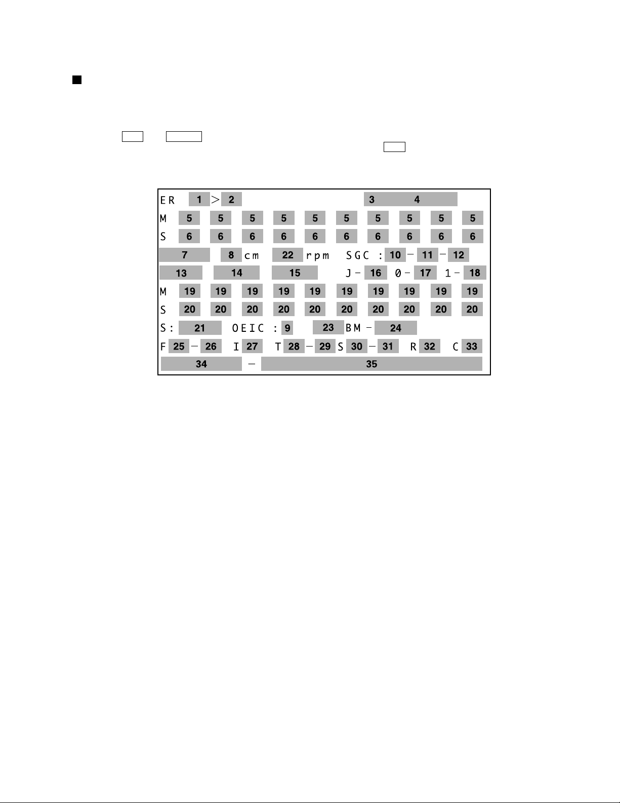
DV-47A, DV-S733A, DV-747A
DEBUGGING SCREEN SPECIFICATION FOR THE MECHANISM CONTROLLER
• This specifications is subject to change without notice.
1 Indication Method of The Mechanism Controller Debugging Screen
A debugging screen of the mechanism controller is indicated when pressing the test mode remote control unit [GGF1067] in
order of the and buttons.
Releace from debugging screen display of the mechanism controller with the button.
2 Screen Layout
ESC
CHP/TM
ESC
3 Indication Contents
1. The error that became the trigger that an error of 2
occurred.
There are many cases same as 2.
2. The error number that transferred to the system
controller
Refer to the error list about contents of error number.
3. Code read in state (it does not support in this unit)
When X is indicated, ID or subcode are not able to read in.
When X is not indicated, they are able to read in.
4. ID or subcode (it does not support in this unit)
Subcode indicates the A time.
5. Inside mode of the mechanism controller when an error
of 1 occurred
It can indicate to a maximum 10 mode. Indicate it in order of
an old mode from the left, and go right, and become a new
mode. Indicate only a nest share of the mode.
6. Processing step of inside mode of 5
It can grasp the mode reaching an error and transition of step
by watching 5 and 6 and it can specify the occurrence place of
most errors.
7. Disk information in the mechanism controller
? : Indistinctness
NO : There is no disc
DVD 1 : DVD single layer
DVD 2 : DVD dual layer
CD : CD
CDR : CD-R or CD-RW
CDR P : PRD of CD-R or CD-RW
8. As a result of 8cm /12cm distinction
? : Indistinctness (undistinction)
8 : 8 cm
12 : 12 cm
9. OEIC gain (it does not support in this unit)
H : OEIC HIGH gain
L : OEIC LOW gain
10. SGC gain for LD of 780nm
It indicates a step using in the mechanism controller inside
with a hexadecimal number.
Set the gain so that S curve becomes 1.8V (p-p) in disc
distinction.
11. SGC gain for LD of 650nm For L0.
It indicates a step using in the mechanism controller inside
with a hexadecimal number. Set a gain so that S curve
becomes 1.8V (p-p) in disc distinction.
12. SGC gain for LD of 650nm For L1.
It indicates a step using in the mechanism controller inside
with a hexadecimal number. Set a gain so that a S curve
becomes 1.8V (p-p) in disc distinction.
13. RF count value for disc distinction
RF count value to use the disc distinction. It compares
threshold value of 14 and 15 and distinguishes the disc.
14. Disc distinction threshold value (DVD and CD)
Threshold value of the disc distinction. Distinguish it from
DVD if bigger than this value, and distinguish it from CD if
small.
83
Page 84

DV-47A, DV-S733A, DV-747A
15. Disc distinction threshold value (CD and unrecorded
disc)
Threshold value of the disc distinction. Distinguish it from
CD if bigger than this value, and distinguish it from an
unrecorded disc if small.
16. Current jitter value
Indicate the value that was read in from the SCRUT (IC701)
in DVD, and indicate the value that was read in from the
servo DSP in CD.
17. Focus balance setting value of L0
18. Focus balance setting value of L1
19. Current mechanism controller inside mode
(it does not support in this unit)
It can indicate to a maximum 10 modes. Indicate only a nest
share of the mode.
20. Processing step of 11 inside modes
(it does not support in this unit)
It can grasp the current mode, the mode reaching it and
transition of step by watching 19 and 20.
21. Spindle control state of SCRUT (IC701)
(it does not support in this unit)
OFF : Motor off condition
A/B : Accelerator and brakes
FG : FG servo
RVP : Rough speed phase servo
ORVP : Rough speed phase servo of offset addition
22. Rotation number of spindle motor
Do not FG read in ? indication (during spindle stop).
23. Tracking error generation system
(it does not support in this unit)
1: 1 beam (DPD)
3: 3 beams
24. TZC count value (it does not support in this unit)
The value that counted the number of TZC for one rotation in
the tracking open state.
When this value is more than 512 with CD, set it in 1 beam
because the eccentric is large.
DVD does not measure it because it is 1 beam fixed
(indication is 0000).
27. It indicates the frequency that entered the internal
circumference plunging into backup of the sled
Hexadecimal number indication. Counter does not reset till
turns the power off after turning it on. Due to a 1 byte
counter, next of FF becomes 00.
28. It indicates the frequency that entered the tracking
overrun backup
Hexadecimal number indication. Counter does not reset till
turns the power off after turning it on. Due to a 1 byte
counter, next of FF becomes 00.
29. It indicates the limit frequency of tracking overrun
backup with a hexadecimal number
Initial value is 03H, it does decrement whenever enter the
tracking overrun backup and it gives up backup if it became
0.
30. It indicates the frequency that entered sled overrun
backup
Hexadecimal number indication. Counter does not reset till
turns the power off after turning it on. Due to a 1 byte
counter, next of FF becomes 00.
31. It indicates the limit frequency of sled overrun backup
with a hexadecimal number
Initial value is 03H, it does decrement whenever enter the
sled overrun backup and it gives up backup if it became 0.
32. It indicates the frequency that entered the tracking close
NG backup
Hexadecimal number indication. Counter does not reset till
turns the power off after turning it on. Next of FF is be a 1
byte counter in 00.
The hexadecimal number indication which indicates the
frequency that reads
33. ID/subQ, and entered NG backup
Hexadecimal number indication. A counter does not reset it
till cuts it off after turning it on. Due to a 1 byte counter, next
of FF becomes 00.
34. An address to indicate in 35
Set it by using RS232.I
(an address) Set it with DA.
35. Contents of an address indicated in 34.
25. It indicates the frequency that entered the focus backup
Hexadecimal number indication. Counter does not reset till
turns the power off after turning it on. Due to a 1 byte
counter, next of FF becomes 00.
26. It indicates focus backup limit frequency with the
hexadecimal number
Initial value is 14H, it does decrement whenever enter the
focus backup and it gives up backup if it became 0. Then the
error is generated. After reverted from the backup, When not
enter the backup and pass fixed time (1500ms), return to
initial value again.
84
Page 85
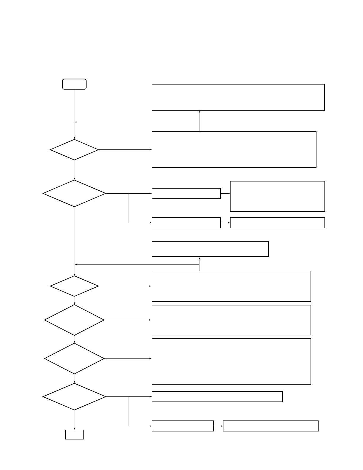
7.1.5 TROUBLE SHOOTING
• No Power ON
• FL is not turned ON
• FL indication is unusual
DV-47A, DV-S733A, DV-747A
START
Turn on the power again
after 2 - 3 minutes.
Is FL turn on ?
Yes
Is the indication
of FL normal ?
Yes
Power ON
No
No
• Blow out fuse of the primary side
• Blow out micro-fuse on the POWER SUPPLY Unit. (Check the each voltage.)
(P101)
• FL controller IC (IC101) on the FLIR Assy is damaged.
• Check the following connections :
POWER SUPPLY Unit - DVDM Assy
DVDM Assy - AVJB Assy
AVJB Assy - FLIR Assy
• Check each voltage (EV+5V, SW+5V, SW+3.3V, SW+12V, +6V and -28V)
(If above voltage are not supplied, check the micro-fuse P101.)
• Short or open the zenner diode
FL indication is dark or flickers.
Indicates the error message
• Blow out micro-fuse on the POWER SUPPLY Unit.
(P101)
on the POWER SUPPLY Unit.
(ZD103, ZD104)
• Check the values of R132 - R134
on the FLIR Assy.
Refer to the section "7.1.6 ERROR CODE".
Is tray open ?
Yes
Spindle
does not turn.
Carriage does
not move.
Yes
Laser diode
does not light.
Focus does
not in.
Yes
Do the video and
sound come on ?
Yes
OK
No
No
No
No
• Check the following connections :
DVDM Assy - LOAB Assy (5P connector assy)
• Check the voltage of +6V and +12V power supply
(If above voltage is not supplied, check the micro-fuse P101.)
• Check the following connections :
DVDM Assy - Spindle motor (12P flexible cable)
DVDM Assy - Stepping motor (4P flexible cable)
• Check the voltage of +6V and +12V power supply
(If above voltage is not supplied, check the micro-fuse P101.)
• Check the following connection :
DVDM Assy - Pickup Assy (26P flexible cable)
• Check the voltage of +6V and +12V power supply and SW+5V
(If the voltage of +6V and +12V power supply are not supplied,
check the micro-fuse P101.)
• Check it whether the pickup is defectiveness.
Perform the section "7.1.2 Self-Diagnostic Function of Pickup Defective"
and check the LD current value.
Check the connection between AVJB Assy and DVDM Assy.
Indicate the error message.
Refer to the section "7.1.6 ERROR CODE".
85
Page 86
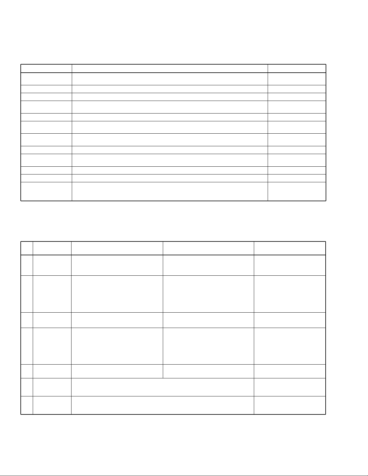
DV-47A, DV-S733A, DV-747A
7.1.6 ERROR CODE
Error codes that are displayed on the FL display without using the remote control unit
FL Display Possible causes Operation of the unit
AV1 VER AV-1 chip is not a match with the program of system controller
CPU AERR CPU address error (Hardware is unusual.) No operation
DMA AERR DMA address error (Hardware is unusual.) No operation
FLASH ID
FLASH WRP Write protect error of the flash ROM No operation
FLASH SIG
FLASH SUM
FLASH SIZE Size error of the flash ROM (Use 4 or 8 M-bit.) No operation
ILLGAL The system controller fetched a code other than an operation code (Hardware is unusual.) No operation
RESERVE Undefined interrupt (Hardware is unusual.) No operation
SLOT Inappropriate slot command issued (Hardware is unusual.) No operation
SDSP PWER Access error to the servo DSP or clock does not oscillation (Hardware is unusual.)
Difference in versions of the internal ROM of the system controller and of the flash ROM,
or bus line failure or reverse installation
Difference in part number of the flash ROM
(When the ROM which could't be used was used.)
Check sum error of the flash ROM (It exceeds the regular size.) or reverse
installation (Hardware is unusual.)
The sound may not out
with the specific audio.
No operation
No operation
No operation
Accept only OFF operation of
the POWER key of the main
unit. Remote control unit is
impossible.
Error codes that are displayed on the FL display by using the remote control unit
(Mechanism controller error)
To display: ESC + DISPLAY + DISPLAY; Location of the display: At the two digits of center of the FL display
To display the error history: ESC + DISPLAY + One shot; Location of the display: TV screen
Description
FL
1C
of Error
11 Search timeout
Search retry
12
error
Tracing timeout
19
while converging
Index 0 search
1B
error
Wobble
distinction error
Timeout of slider
22
inner circumference
Timeout of slider
23
outer
circumference
Search could not be complete within 7
seconds.
A search could not be completed after 3
retries, search backup was executed 4
times, or in a case of timeout (6 seconds)
while the unit was tracing 11 tracks or
more beyond the target while the search
operation was converging.
Timeout (10.5 seconds) while tracing at
the stage of convergence of a search.
Distinguished RW disc without wobble.
Inside switch could not ON within 3 seconds.
Inside switch could not OFF within 2 seconds. Stop
Causes if with a DVD Causes if with a CD Operation of the Unit
Search could not be complete within 7
seconds, and it could not enter the target
area within 7 seconds by VCD scan.
Backup against slider skip was executed
4 times during a search, or slider skip
twice resulted in starting from the read-in
point.
During Track (Index) Search, the search
for the beginning of a program could not
be completed within 3 seconds (20
seconds in the case of Index Search)
after positioning based on the TOC data
was completed.
CD : Stops,
DVD : Continues operation
CD : Stops,
DVD : Continues operation
Stop
Stop
Read the RW control data.
Stop
86
Page 87
DV-47A, DV-S733A, DV-747A
Description
FL
33
38
39
41 Spindle timeout The unit did not enter Stop mode within 10 seconds of issuance of a Stop command. Stop
48
49
4A Spindle lock timeout Spindle could not lock more than 1.5 seconds before start the AFB.
51
52
53
54
55
56
57
58
59
5A
5B
of Error
No FOK pulse during
playback CLVA
Disc-typesensing error
SGC converge
timeout
Spindle FG
transition timeout
Spindle PLL
transition timeout
Auto sequence
timeout of peak
detection
Auto sequence
timeout of focus
jump down
Auto sequence
timeout of focus
jump up
Auto sequence
timeout of play AGC
Auto sequence
timeout of disc-typesensing
Auto sequence
timeout of ATB2
Auto sequence
timeout of tracking
servo ON
Auto sequence
timeout of ATB1
Auto sequence
timeout of focus gain
adjustment
Auto sequence
timeout of tracking
gain adjustment
Auto sequence
timeout of offset
adjustment
When the focus was deviated continuously 20 times.
If normal starting was impossible in the following three cases, disc-type sensing will be
retried if other errors occure excepting C5 error. However, when the focus error "33"
was occured continuously 3 times, it is finished as "38 error" at the moment:
(1) startup with the first disc-type-sensing result, (2) forced startup with another disc by
designating the disc type, (3) forced startup with the original disc by designating the disc
type.
SGC could not converge during detects the peak Open
The spindle could not converge into within ± 12% of
the target FG rotation speed within 10 seconds after
spindle kick. The first time after startup (the first time
after disc distinction), it doesn't become the number of
the target rotation within five seconds. The first time
after startup, detects the abnormal rotation number of
high-speed continuously 3 loops. DVD: 5 to 9 mS ,
CD: 40 to 60 mS
After the second times after startup, it doesn't become the number of the target rotation
within five seconds. Detects the abnormal high-speed or low-speed rotations.DVD: 5 to
9 mS , CD: 40 to 60 mS
ABUSY did not return within 1 second after the
DDTCT (peak detection) command was sent.
ABUSY did not return within 30 mS after the FJMPD
(Focus jump 1 to 0) command was sent.
ABUSY did not return within 30 mS after the FJMPU
(Focus jump 0 to 1) command was sent.
ABUSY did not return within 50 mS after the GSUMON
(play-AGC-measuring) command was sent.
ABUSY did not return within 2 seconds after the
DJSRT (disc-sensing) command was sent.
ABUSY did not return within 1 second after the
TBLOFS (Internal ATB after the completion of external
ATB) command was sent.
ABUSY did not return within 500 mS after the TSON
(tracking servo ON) command was sent.
ABUSY did not return within 200 mS after the TBL
(external ATB) command was sent.
ABUSY did not return within 2 seconds after the FGN
(focus gain adjustment) command was sent.
ABUSY did not return within 2 seconds after TGN
(tracking gain adjustment) command was sent.
ABUSY did not return within 1 second after the
CMDAVE (offset adjustment) command was sent.
Causes if with a DVD Causes if with a CD
Adjusts focus at the
innermost circumference
and tries to return to its
position where the error
was generated (for 3
times),then opens. If the
same error persists after
one retry, the tray opens.
(No FOK pulse)
Open
Stops. (FG timeout)
Stops.
("73" is displayed during
starting process.)
Stops.
("73" is displayed during
starting process.)
Stop
Stop
Stop
Stop
Stop
Stop
Stop
Stop
Stop
Stop
Stop
Operation
of the Unit
87
Page 88
DV-47A, DV-S733A, DV-747A
Description
FL
5C
5D
5F
62 Pause retry error
71
72
73
74
81
82
A1
A2
A3
A4
B1
B2
B3 Retry error for trace
C3
(C5)
E3
of Error
Auto sequence
timeout of
modulation factor
measurement
Auto sequence
timeout of auto focus
bias
Auto sequence
already busy
ID can not read
during tracing
Subcode check
failure during
playback
ID can not read at
the startup
Subcode check
failure during startup
Timeout for reading
TOC of the
mechanism
controller
Timeout for reading
TOC of the system
controller
Communication
timeout of DSP
command
Communication
timeout for reading
DSP coefficient
Communication
timeout for writing
DSP coefficient
Communication
timeout for
continuously writing
DSP coefficient
Timeout error for
backup
Retry error for
backup
Detection of tracking
overcurrent
Short-circuit test
corresponding error
Violation against
digital copy guard
Causes if with a DVD Causes if with a CD
ABUSY did not return within 200 mS after the
ADJMIR (modulation factor measurement)
command was sent.
ABUSY did not return within 2 seconds after the
AFB (auto focus bias) command was sent.
A command could not be sent because ABUSY
was low. ABUSY did not return within 200 mS
after TLV command was sent.
Pause mode could not be restored within three
retries after it had been released.
An ID could not be read for 1 second or more. Stop
No frame could be read for 3
seconds or more.
An ID could not be read within 1 second after the
AFB adjustment had been finished.
No subcode could be read within 3
seconds after AFB adjustment had
been finished.
TOC readout took 30 seconds or
more.
Reading TOC of the system
controller took 30 seconds or more.
A command could not be issued to DSP because
Command Busy (XCBUSY) was in force
(XCBUSY = L) for a specified time (about 200
mS).
Command Busy (XCBUSY) was in force for a
specified time (about 200 mS) before and after a
coefficient read command was issued to DSP, or
the address echo-back after command issuance
did not match the setup address.
Command Busy (XCBUSY) was in force for a
specified time (about 1024 mS) before and after
the coefficient write command was issued to
DSP.
Command Busy (XCBUSY) was in force for 200
µS during continuous coefficient writing, or
before and after a continuous write command
was issued to DSP.
In the tracing state during the backup sequence, codes could not be read for 1
second or more. In the backup sequence, tracking ON sequence of the servo DSP
could not be completed even if more than 500 mS after the tracking ON command
was issued.
Tracing impossible after retring the tracking ON for 3 times in the backup sequence. Stops
During tracing, runaway was detected after three iterations of backup operations for
detecting runaway.
During playback, the overcurrent detection port was at L for 300 ms or more
continuously.
While the power was on, the overcurrent detection port was at L for 40 ms or more
continuously.
Stop
Stop
Stop
Continues operation
Stop
Opens (ID readout failure)
Opens (Subcode readout
failure).
Stop
Stop
Open
Open
Open
Open
Stops
Stops
Stops (the mechanical
controller operates
independently).
Turns off the power
instantly (No indication on
the FL display and no
writing to flash memory)
Stops
Operation
of the Unit
88
Page 89
DV-47A, DV-S733A, DV-747A
Description
FL
F5 Tray being pushed
F8 Loading timeout
FC Focus
of Error
The tray switch that had been Open mode was forcibly changed to a mode other than
Open by an external force.
Loading, unloading or clamping could not be completed within a specified time (about
5 seconds).
The following error occured eight times.
(1) Focus ON sequence could not be completed even if more than two seconds after
(2) Focus IN sequence was finished, actually focus IN was not completed.
Causes if with a DVD Causes if with a CD Operation of the Unit
Closes
Reverses the loading
direction. It timeout is
repeated upon retry, the
unit stops.
Stops wherever possible
the focus ON command (to the servo DSP) was sent.
then opens (stops in the
case of side B).
Error codes that are displayed on the FL display by using the remote control unit (Device error)
To display : ESC + DISPLAY + DISPLAY ; Location of the display : At the two digits of left of the FL display
FL Description of Error Causes if with a DVD Causes if with a CD Operation of the Unit
bit3=1 08 etc.
bit2=1 04 etc. MY CHIP access error
bit1=1 01 etc. SRAM access error
AV1 access error
(read, write NG)
No operation or it becomes debugging
indication if the power is able to ON.
89
Page 90
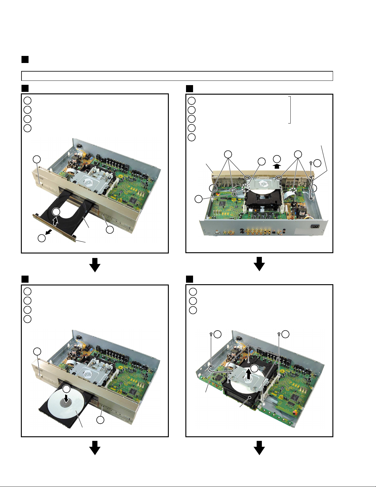
DV-47A, DV-S733A, DV-747A
7.1.7 DISASSEMBLY
DIAGNOSIS OF PCBs
Note
When diagnosing the unit, be sure to use two connection cables for service. (Part No. : GGD1271)
1
Bonnet and Tray Panel
Remove the Bonnet (Screws × 7)
1
Power ON
2
Tray open (0)
3
Remove the Tray Panel
4
2
4
3
Tray
Door
3
Front Panel
Unclamp the wire.
1
Disconnect the wiring.
2
Remove the Earth Lead Unit (Screw × 1).
3
Unhook (×6)
4
Remove the Front Panel.
5
×3
Front Panel
4
2
5
Except DV-47A
Earth Lead Unit
×3
4
3
1
3
2
Test Disc Set
Set the Test Disc
1
Tray close (0) → Clamp the Test Disc
2
Power OFF
3
Pull out the Power Cord from the outlet
4
3
1
Test Disc
4
Loading Mechanism Assy
Remove the Earth Lead Unit (Screw × 1).
1
Remove four screws.
2
Remove the Loading Mechanism Assy.
3
(Remove the Connector (×2).)
× 4
1
2
3
Earth Lead Unit
Loading
Mechanism
2
Assy
90
Page 91
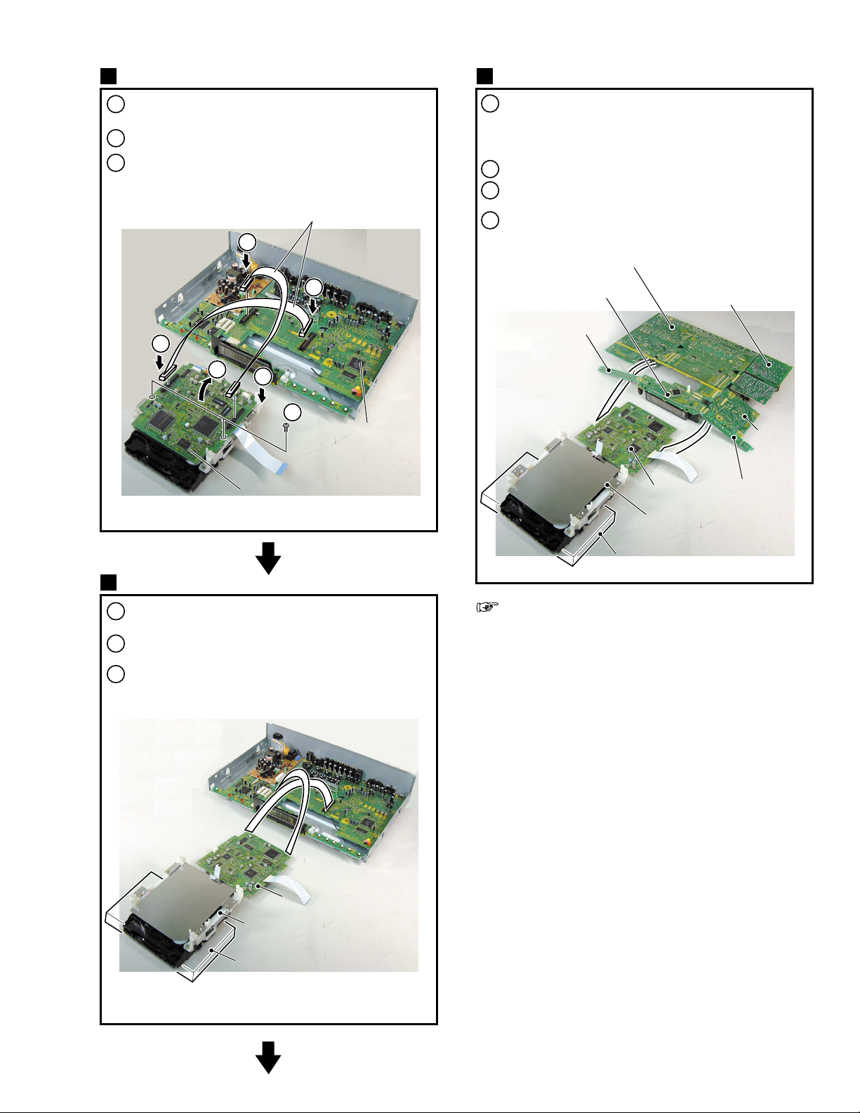
DV-47A, DV-S733A, DV-747A
AVJB Assy
Loading Mechanism Assy
Spacer
DVDM Assy
DVDM Assy
KEYB Assy
PWSB Assy
SACD Assy
Loading Mechanism Assy
(×2)
DVDM Assy
Styling of the Connection Cables
5
Connect two Connection Cables for Service (GGD1271)
1
between DVDM Assy and AVJB Assy.
Remove two screws.
2
Remove the DVDM Assy.
3
Connection Cable
for Service
[GGD1271]
1
1
1
3
Diagnosis (1)
6
Arrange the Loading Mechanism Assy and the DVDM Assy
1
like the figure below.
Put in spacers under the Loading Mechanism Assy not to
2
rub the Clamper.
Playback with a test disc, and diagnose the DVDM Assy
3
and the other Assys.
1
2
DVDM Assy
(×2)
AVJB Assy
Diagnosis (2)
7
Unscrew the Rear Panel and remove the Rear Panel.
1
Cautions:
Please install AC inlet Assy in POWER SUPPLY Unit
once again after having detached it with a rear panel.
Unscrew the PCBs and remove the PCBs.
2
Arrange the Loading Mechanism Assy and the PCBs
3
like the figure below.
Playback with a test disc, and diagnose the AVJB Assy
4
and the other Assys.
AVJB Assy
FLIR Assy
KEYB Assy
Spacer
POWER SUPPLY Unit
DVDM Assy
Loading Mechanism Assy
In a diagnosis (1) (2), You cannot play SACDs.
SACD Assy
PWSB Assy
Spacer
DVDM Assy
Loading Mechanism Assy
91
Page 92
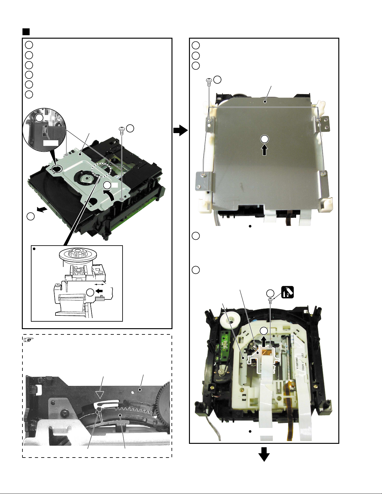
DV-47A, DV-S733A, DV-747A
Disassembly of the Traverse Mechanism Assy and the Pickup Assy
Remove the Bonnet and Tray Panel.
1
Remove the Front Panel.
2
Remove the Loading Mechanism Assy (Screws ×4).
3
Remove the Bridge (Screw ×2).
4
Pull out the Tray and remove it while unhooking a Hook.
5
Turn the Short SW to Short side.
6
-1
5
×2
4
-1
-2
-2
5
RearView
Bridge
Hook
4
Remove the DVDM Assy (Screws ×2).
7
Remove four screws.
8
Remove the Mechanism Holder.
9
×4
8
Mechanism Holder
9
Bottom View
Remove a screw.
10
Cautions:
Screw is locked with Silicone adhesive.
Please lock it with Silicone adhesive when installs it.
Short
Open
6
Short SW
Caution in the tray insertion
In the Tray insertion, insert it after matching a triangle mark
of the Loading Base and a position of pin of the Drive Cam.
Triangle mark
Loading Base
Remove the FFC Holder with the state which Flexible Cable
11
was atatched.
FFC Holder
10
Traverse Mechanism
Assy
Silicone Adhesive
GEM1037
11
Bottom View
92
Drive CamPin
Page 93
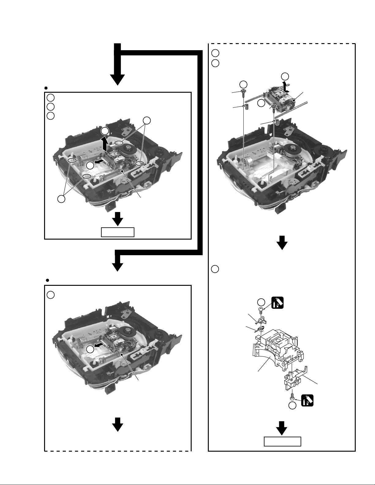
DV-47A, DV-S733A, DV-747A
Pickup Assy
Traverse
Mechanism Assy
When Removing The Traverse Mechanism Assy
Remove the Pickup Flexible Cable
12
Unhook ( ×4)
13
Remove the Traverse Mechanism Assy
14
13
× 2
14
12
× 2
13
Traverse Mechanism
Assy
Remove two Skew Screws and two Skew Springs.
13
Remove the Pickup Assy.
14
14
Skew
Screw
Skew
Spring
13
Skew
Spring
13
Skew
Screw
Pickup Assy
Exchange
When Removing The Pickup Assy
Remove the Pickup Flexible Cable.
12
12
Traverse Mechanism
Assy
Remove two screws.
15
Cautions:
Screw is locked with Silicone adhesive.
Please lock it with Silicone adhesive when installs it.
15
Slider
Hold Spring
Pickup Assy
Silicone Adhesive
GEM1037
15
Joint
Silicone Adhesive
GEM1037
Exchange
93
Page 94
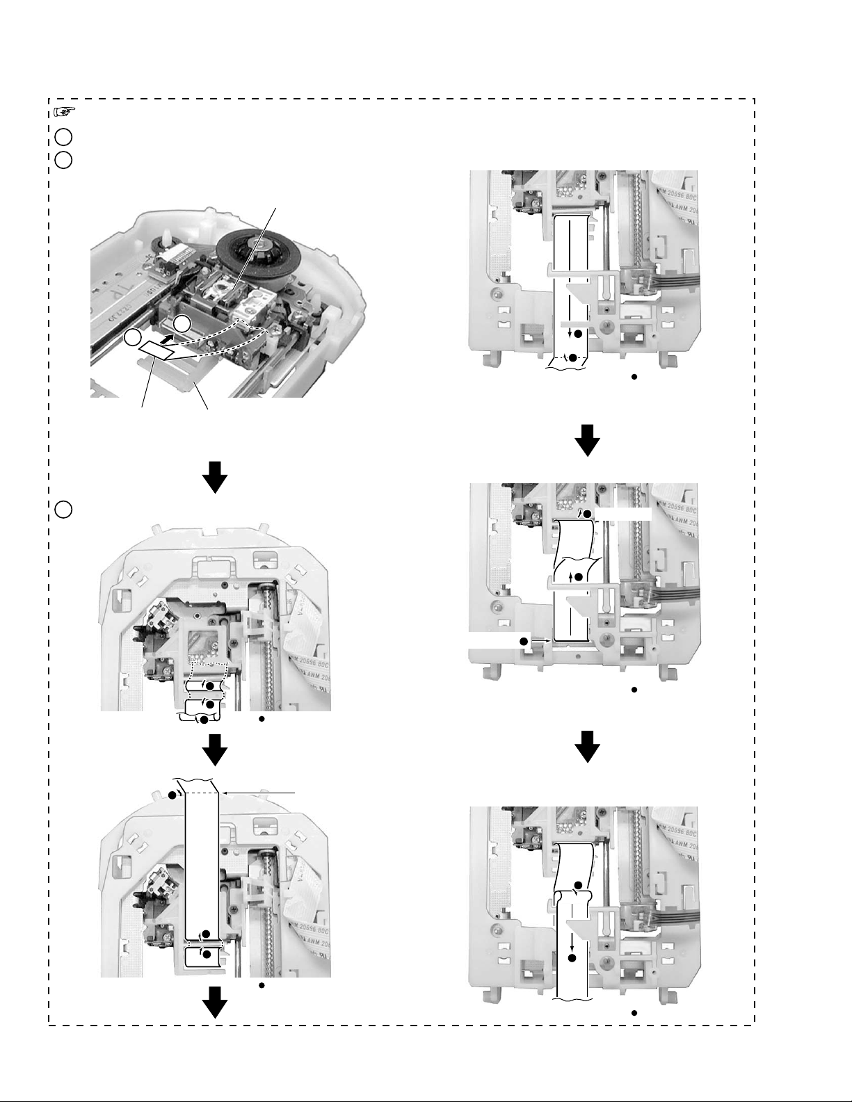
DV-47A, DV-S733A, DV-747A
Styling the Pickup Flexible Cable
Fold a edge of lining part of the Pickup Flexible Cable.
1
Insert the Pickup Flexible Cable in connector, and lock it surely.
2
Pickup Assy
1
2
Conducting plane
Caution:
Move the Pickup to the innermost of the disc.
Perform the styling as shown in figure below.
3
FFC Holder
1
2
3
Bottom View
Fold position of step
7
8
Bottom View
10
Lose slack
9
6
Bottom View
Fold it at the position
of reference line.
94
6
5
5
4
Reference line
11
12
Bottom View
Bottom View
Page 95
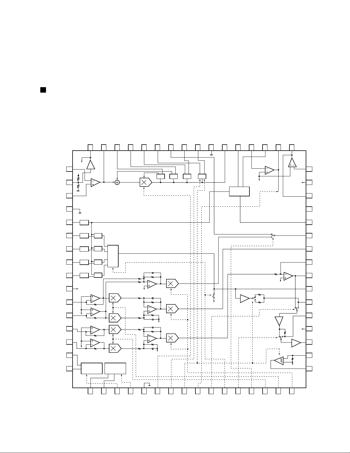
DV-47A, DV-S733A, DV-747A
7.2 IC
• The information shown in the list is basic information and may not correspond exactly to that shown in the schematic diagrams.
List of IC
•
LA9701M, LC78652W, BA6664FM, PD6345A, M65774BFP, XCA5636PV150, ADV7300KST, PM0033A, PE5251A, CXD2753R
LA9701M (DVDM ASSY : IC101)
• RF IC
Block Diagram
•
REF
RFOUT
PHC
BHC
PHI
BHI
AUX
PH
BH
GND
RFO
TC
EQI1
DEFC
EQO1
EQO2
64
63
62
61
60
59
58
57
56
55
54
53
52
51
50
49
PDRF–
REF1
RF1
GND
PDRF
PD1
PD2
PD3
PD4
VCC
FIN1
FIN2
PD5
10
11
12
13
REF
1
VCC
2
3
4
5
LIM
6
7
8
9
REF
LIM
LIM
LIM
LIM
VCC
PD
PD
PD
PD
CP
REF
PH
BH PH BH
REF
REF
Scratch
Detection
DVD
REF
REF
CD
VCC
VCC
48
47
46
45
44
43
42
41
40
39
38
37
36
EQI2
VCC
EFMO
N/C
DEF
RREC
FE
TE–
TEO
CP
TLP
THC
VCC
PD6
LDD1
LDS1
14
15
16
REF
DVD
APC
17
LDD2
CD
APC
18
LDS2
19
LDON1
20
LDON2
21
GND
REF
22
AGOF
23
XQBH
24
XHTR
25
DVD/CD
26
DPD/TE
27
CPOF
28
TH
29
AUX/RR
30
TEBAL
31
FFBAL
REF
32
SGC
35
34
33
TE
TESI
TES
95
Page 96
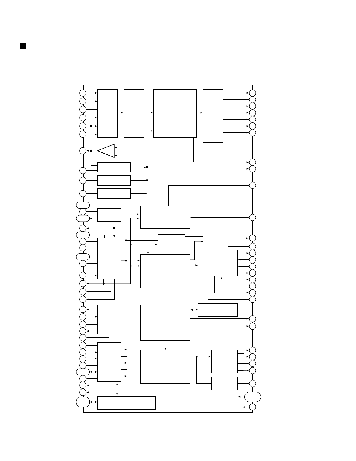
DV-47A, DV-S733A, DV-747A
LC78652W (DVDM ASSY : IC201)
• Servo DSP IC
Block Diagram
•
TILTE
RF_PH
RF_BH
JITT
HFLIO
TES
PP2/EVENT
FG
SLCIST1,2
EFMIN
SLCO1,2
EFMOUT
PCKIST1,2
DVDFR
CDFR
PD01-3
DVDSYNC
PCK
LEFM
LEFM2
VPDO
VCOC
XIN
XOUT
XTALOUT
ADRAO
CSB
WRB
RDB
P0-7
BUSYB
LASER
FBUSYB
PP0-3
FE
TE
JV
33
32
29
30
31
28
51
26
56
55
34,35
39
36,37
1
87,88
90
91
83-85
92
96
93
100
97
81
80
14
15
8
94
58
60
59
63-70
73
52
7
53,54
,56
MPX
8bit
A/D
CMP
Track Counter
Event Counter
FG Counter
SLC
PLL
Frame Synchronous
Detection, Protection,
Clock
Generator
Command
Interface
General Purpose Register
Servo
Processor
(16×16+32→32)
CLV
DVD Lock
Detection
Insertion EFM
Demodulation
Error Detect
Correction
C1-Twofold,
C2-Fourfold
Supplement/Mute
D Attenuate
Deemphasis Filter
8bit
D/A
Sub Code
Decode
CRC
For De-Interleave
16k SRAM
Serial Out
DOUT
47
48
45
46
44
43
42
24
22
95
23
21
77
74
75
76
17
12
10
18
11
9
20
5
4
3
2
19
25,27
38,50
57
FDO
TDO
SLDO
SPDO
TBAL
TILTDO
AUXO
DRF
FAST
DVDSYEQ
V_PB
FSEQ
WRQ
SQOUT
CQCKB
RWC
EMPH
PW
SBCK
SBSY
SFSY
FSX
EFLG
LRSY
ROMCK
ROMXA
C2F
DOUT
TEST1-4
RESB
96
Page 97
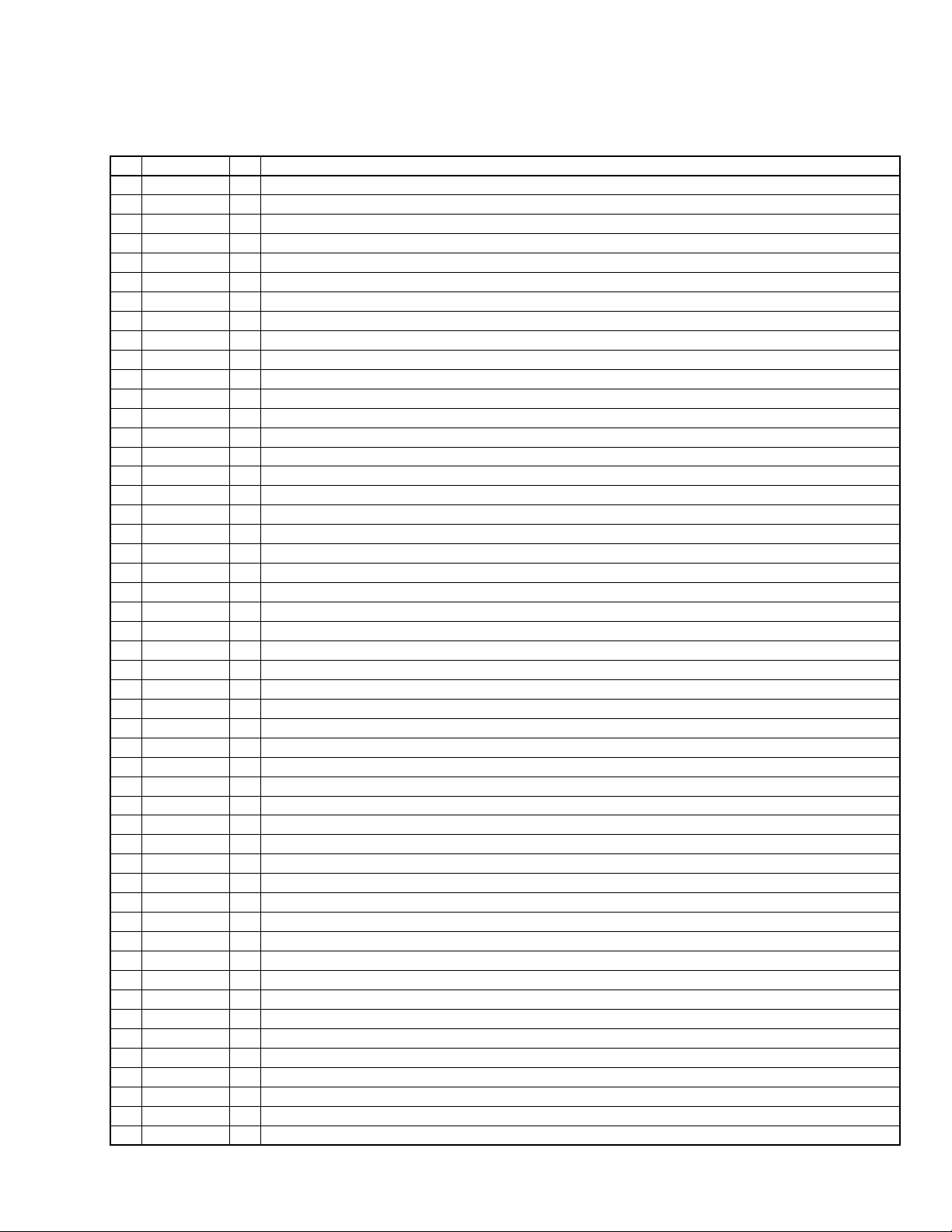
Pin Function
•
.oNemaNniPO/InoitcnuFniP
1TUOMFEO MFEeulavdetats-yranibsawtahtetatsehttuptuO
2F2COtuptuogalf2C
3AXMORO tuptuoatadMOR-DC
4KCMORO tuptuoatadMOR-DCroftuptuokcolctfihS
5YSRLO tuptuoatadMOR-DCroftuptuokcolcR/L
63PPO/I tuptuoDO-hcNtupnilangis.cnysDVD/tuptuo/tupnitropesoprup-lareneG
7BYSUBFO tuptuoDO-hcNnoitarepossecorpPSDfotuptuolangisysuB
8TUOLATXO tuptuokcolcmetsyslanretxE
9XSFO tuptuolangis.cnysemarf1DC
01KCBSI tupnikcolctuognidaeredocbuS
11YSFSO edocbusfotuptuolangis.cnysemarF
21WPO tuptuoWdnaV,U,T,S,R,Q,PedocbuS
31SSV
41NIXI )zHM4439.61(rotanoserlatsyrcatcennoC
51TUOXO rotanoserlatsyrcatcennoC
611DDVD
71HPMEO sisahpmeedehtfoniprotinoM
81YSBSO kcolbedocbusehtfotuptuolangis.cnyS
91TUODO tuptuoatadJAIEoiduA
02GLFEO 2Cdna1CnoitcerrocrorreehtforotinometatsnoitcerrocrorrE
12QESFO langis.cnysemarfDVD/DCehtforotinomnoitceteD
22TSAFO tuptuoDO-hcNrotinomdeepskcabyalP
32BP_VO lortnocVLC/ovreshguorehtfotuptuorotinoM
42FRDO rotinomsucofnI
523TSETI3tupnitseT
62SETI tupnilangisrorregnikcarT
722TSETI2tupnitseT
82TTIJI LLPMFEfotupnilangisgnitcetedytitnauqrettiJ
92ETLITI tupnilangisrorretliT
03HP_FRI tupnilangisdlohkaepFR
13HB_FRI tupnilangisdlohmottobFR
23
ET
33EFI tupnilangisrorresucoF
431TSICLS
532TSICLS
631OCLSO CLSrof1tuptuolortnoC
732OCLSO CLSrof2tuptuolortnoC
831TSETI1tupnitseT
93NIMFEI tupni+MFE/MFE
04DDVA
14SSVA
24OXUAO tuptuoyrailixuaAD
34ODTLITO tuptuolangislortnoctliT
44LABTO tuptuolangislortnocecnalabgnikcarT
54ODLSO tuptuolangislortnocdelS
64ODPSO tuptuolangislortnoceldnipS
74ODFO tuptuolangislortnocsucoF
84ODTO tuptuolangislortnocgnikcarT
94FERV
054TSETI4tupnitseT
−
−
ItupnilangisrorregnikcarT
−
−
−
−
−
nipDNG
ovresrofA/DdnaD/AfoylppusrewopV5
ovresrofA/DdnaD/AfoDNG
ovresrofA/DfolevelecnerefeR
DV-47A, DV-S733A, DV-747A
tiucricnoitallicsoehtfoylppusrewopV3.3
CLSrofpmupegrahctnerructnatsnocehtfo1nipgnittestnerruC
CLSrofpmupegrahctnerructnatsnocehtfo2nipgnittestnerruC
97
Page 98
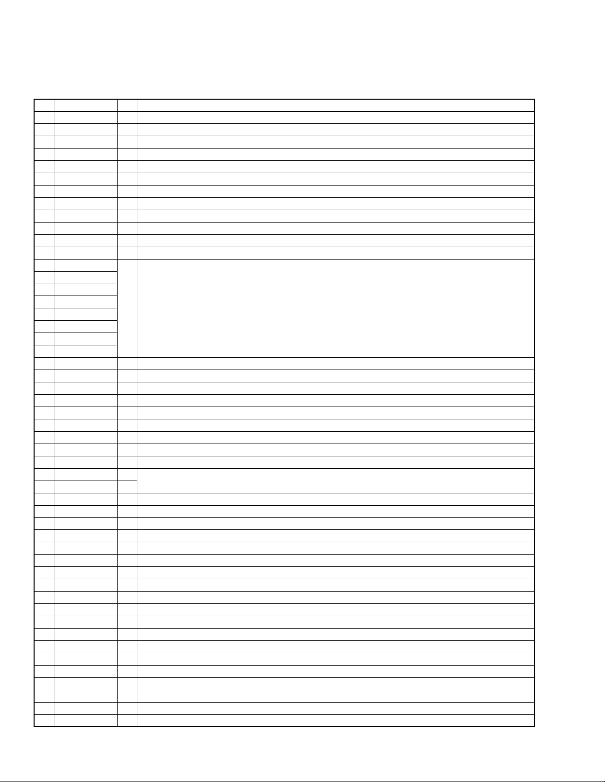
DV-47A, DV-S733A, DV-747A
.oNemaNniPO/InoitcnuFniP
15OILFHO/Ituptuo/tupnilangisnoitcetedrorriM
25RESALO lortnocFFO/NOresalrofniptuptuO
35BDC_DVD/0PPO/ItuptuolangisnoitanimircsidcsiD/tuptuo/tupnitropesoprup-lareneG
45BRRECRC/1PPO/I tuptuolangistluserCRCedocbuS/tuptuo/tupnitropesoprup-lareneG
55GFI tupniretnuocGF
65TNEVE/2PPO/ItupniretnuoctnevE/tuptuo/tupnitropesoprup-lareneG
75BSERItupniteseR
85BSCI tupnitcelespihC
95BDRI tupnilangisgnidaeretatslanretnI
06BRWI tupnilangisgnitirwatad/dnammoC
162DDVD
26SSV
360P
461P
562P
663P
764P
865P
966P
077P
17SSV
271DDVD
37BYSUBO ssecorpdnammocfotuptuolangisysuB
47TUOQSO QedocbusfotuptuolaireS
57BKCQCI tuptuoatadQedocbusroftupnikcolctfihS
67CWRI QedocbusfotupninoissimrepetadpU
77QRWO QedocbusforotinomydaertuodaeR
87SSVA
97RFPRV
08COCVI
18ODPVO
28
DDVA
381ODPO/IkcabyalpMFErof1nipnoitcennocretlifLLP
482ODPO/IkcabyalpMFErof2nipnoitcennocretlifLLP
583ODPO/IkcabyalpMFErof3nipnoitcennocretlifLLP
68SSVA
781TSIKCP
882TSIKCP
98DDVA
09RFDVD
19RFDC
29VJO kcabyalpMFErofkcolcLLPfotuptuorettiJ
39KCPO kcabyalpMFEroftuptuokcolctiB
49OARDAItupnisserddA
59QEYSDVDI tupnieslupezinorhcnysDVD
69CNYSDVDI tupnilangissuonorhcnysDVD
792MFELO 2KCPhtiwMFEeulavdetats-yranibsawhcihwlangisatuodnatuctahtetatsehttuptuO
891DDVD
99SSV
001MFELO 1KCPhtiwMFEeulavdetats-yranibsawhcihwlangisatuodnatuctahtetatsehttuptuO
−
−
O/Ituptuo/tupniatad/dnammoC
−
−
−
−
−
−
−
−
−
−
−
−
−
DNG
DNG
DNG
ylppusrewopV5
lanretnirofylppusrewopV3.3
kcolcmetsyslanretnirofDNGLLP
kcolcmetsysrofretlifLLPatcennoC
kcolcmetsysrofylppusrewopV5LLP
kcabyalpMFErofDNGLLP
kcabyalpMFErofylppusrewopV5LLP
O/IrofylppusrewopV3.3
kcolcmetsysrofLLPfognittesegnarnoitallicsoOCV
kcabyalpMFErofpmupegrahctnerructnatsnocLLPfo1gnittestnerruC
kcabyalpMFErofpmupegrahctnerructnatsnocLLPfo2gnittestnerruC
1kcabyalpMFErofLLPfognittesegnarnoitallicsoOCV
2kcabyalpMFErofLLPfognittesegnarnoitallicsoOCV
98
Page 99
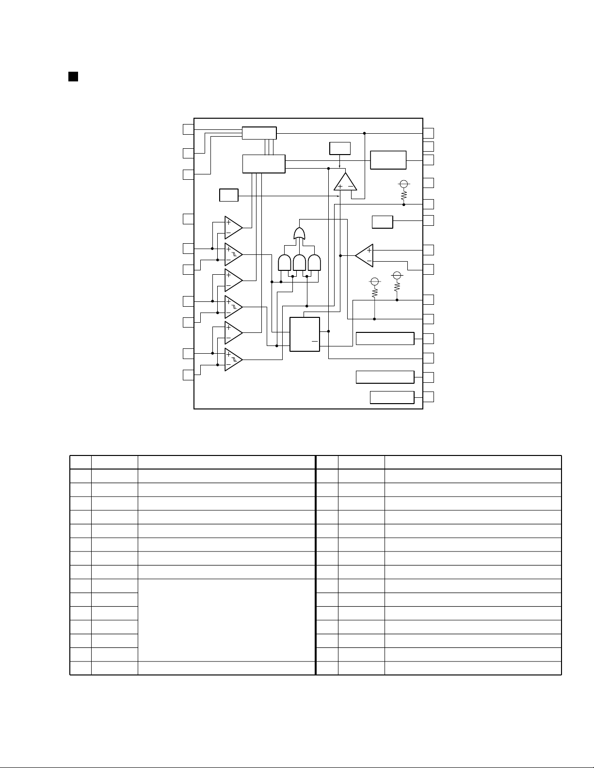
BA6664FM (DVDM ASSY : IC251)
• Three-phase Motor Driver
Block Diagram
•
2
A3
4
A2
7
A1
TL
HALL AMP
8
GND
DRIVER
GAIN
CONTROL
CURRENT
SENSE AMP
TSD
DV-47A, DV-S733A, DV-747A
28
RNF
27
VM
GAIN
SWITCH
TORQUE
PS
Vcc
26
25
24
23
GSW
VCC
FG
PS
SENSE AMP
Vcc
Vcc
SHORT BRAKE
BRAKE MODE
HALL BIAS
22
21
20
19
18
17
16
15
EC
ECR
FR
FG2
SB
CNF
BR
VH
Block Diagram
•
H1+
H1-
H2+
H2-
H3+
H3-
10
11
12
13
14
9
DRQ
CK Q
No. Pin Name Pin NamePin Function No. Pin Function
1 N.C. N.C. 16 BR Brake mode switching pin
2 A3 Output pin 17 CNF Capacitor connection pin for phase compensation
3 N.C. N.C. 18 SB Short brake pin
4 A2 Output pin 19 FG2 FG 3-phase mix signal output pin
5 N.C. N.C. 20 FR Rotation detecting pin
6 N.C. N.C. 21 ECR Control reference pin of output voltage
7 A1 Output pin 22 EC Output voltage control pin
8 GND GND pin 23 PS Power save pin
9H1+
10 H1- 25 VCC Power supply pin
11 H2+ 26 GSW Gain switching pin
12 H2- 27 VM Motor power pin
13 H3+ 28 RNF
14 H3- FIN FIN GND
15 VH Hall bias pin
Hall signal input pins
24 FG FG signal output pin
Resistor connection pin for output current detection
99
Page 100
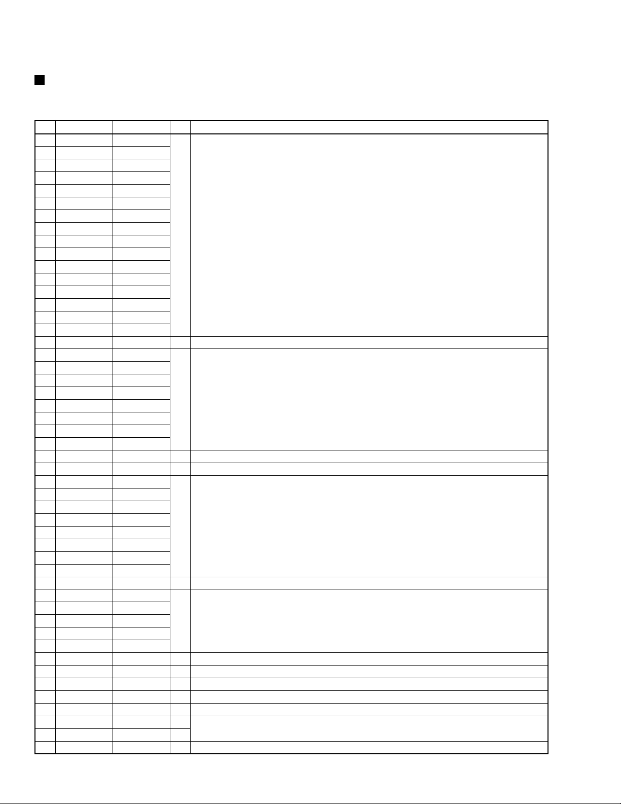
DV-47A, DV-S733A, DV-747A
PD6345A (DVDM ASSY : IC601)
• FR CPU
Pin Function
•
.oNkraMemaNniPO/InoitcnuFniP
161D/02P0D
271D/12P1D
381D/22P2D
491D/32P3D
502D/42P4D
612D/52P5D
722D/62P6D
832D/72P7D
942D/03P8D
0152D/13P9D
1162D/23P01D
2172D/33P11D
3182D/43P21D
4192D/53P31D
5103D/63P41D
6113D/73P51D
71SSVDNG
8100A/04P0A
9110A/14P1A
0220A/24P2A
1230A/34P3A
2240A/44P4A
3250A/54P5A
4260A/64P6A
5270A/74P7A
623CCVD3.3+V
722CCVD5.2+V
8280A/05P8A
9290A/15P9A
0301A/25P01A
1311A/35P11A
23
3331A/55P31A
4341A/65P41A
5351A/75P51A
63SSVDNG
7361A/06P61A
8371A/16P71A
9381A/26P81A
0491A/36P91A
1402A/46P02A
2412A/56PATSFOTO ovresrofA-noitcejnitesffognikcarT
3422A/66PCTSFOTO ovresrofC-noitcejnitesffognikcarT
4432A/76PLBWO )niam(W/RDVDotgnidnopserrocnoitcetedelbboWroF
54SVADDNG
64CVADD3.3+V
740AD1PETSI
841AD2PETSI
942ADVRDOLI evirdrotomtcelesdnarood,gnidaoL
21A/45P21A
O/Ituptuo/tupnisubataD
−
OtuptuosubsserddA
−
−
OtuptuosubsserddA
−
OtuptuosubsserddA
−
−
dnuorG
ylppusrewoP
ylppusrewoP
dnuorG
dnuorG
ylppusrewoP
lortnocrotomgnippetsroF
100
 Loading...