

Page 1
CD RECEIVER
ORDER NO.
CRT4037
DEH-P3000IB/XS/UC
DEH-P3000IB
DEH-P3000IB
This service manual should be used together with the following manual(s):
Model No. Order No. Mech.Module Remarks
CX-3195 CRT3815 S10.5COMP2 CD Mech. Module : Circuit Descriptions, Mech. Descriptions, Disassembly
/XS/ES
/XS/UC
For details, refer to "Important Check Points for Good Servicing".
PIONEER CORPORATION 4-1, Meguro 1-chome, Meguro-ku, Tokyo 153-8654, Japan
PIONEER ELECTRONICS (USA) INC. P.O. Box 1760, Long Beach, CA 90801-1760, U.S.A.
PIONEER EUROPE NV Haven 1087, Keetberglaan 1, 9120 Melsele, Belgium
PIONEER ELECTRONICS ASIACENTRE PTE. LTD. 253 Alexandra Road, #04-01, Singapore 159936
PIONEER CORPORATION 2007
K-ZZW. NOV. 2007 Printed in Japan
Page 2

1234
SAFETY INFORMATION
CAUTION
A
This service manual is intended for qualified service technicians; it is not meant for the casual do-it-yourselfe.
Qualified technicians have the necessary test equipment and tools, and have been trained to properly and safely repair
complex products such as those covered by this manual.
Improperly performed repairs can adversely affect the safety and reliability of the product and may void the warranty.
If you are not qualified to perform the repair of this product properly and safely, you should not risk trying to do so
and refer the repair to a qualified service technician.
WARNING
This product contains lead in solder and certain electrical parts contain chemicals which are known to the state of
California to cause cancer, birth defects or other reproductive harm.
Health & Safety Code Section 25249.6 - Proposition 65
B
- Safety Precautions for those who Service this Unit.
When checking or adjusting the emitting power of the laser diode exercise caution in order to get safe, reliable
results.
Caution:
1. During repair or tests, minimum distance of 13 cm from the focus lens must be kept.
2. During repair or tests, do not view laser beam for 10 seconds or longer.
C
CAUTION
Danger of explosion if battery is incorrectly replaced.
Replaced only with the same or equivalent type recommended by the manufacture.
Discord used batteries according to the manufacture's instructions.
D
E
F
2
1234
DEH-P3000IB/XS/UC
Page 3
5 678
[Important Check Points for Good Servicing]
In this manual, procedures that must be performed during repairs are marked with the below symbol.
Please be sure to confirm and follow these procedures.
1. Product safety
Please conform to product regulations (such as safety and radiation regulations), and maintain a safe servicing environment by
following the safety instructions described in this manual.
1 Use specified parts for repair.
Use genuine parts. Be sure to use important parts for safety.
2 Do not perform modifications without proper instructions.
Please follow the specified safety methods when modification(addition/change of parts) is required due to interferences such as
radio/TV interference and foreign noise.
3 Make sure the soldering of repaired locations is properly performed.
When you solder while repairing, please be sure that there are no cold solder and other debris.
Soldering should be finished with the proper quantity. (Refer to the example)
4 Make sure the screws are tightly fastened.
Please be sure that all screws are fastened, and that there are no loose screws.
5 Make sure each connectors are correctly inserted.
Please be sure that all connectors are inserted, and that there are no imperfect insertion.
6 Make sure the wiring cables are set to their original state.
Please replace the wiring and cables to the original state after repairs.
In addition, be sure that there are no pinched wires, etc.
7 Make sure screws and soldering scraps do not remain inside the product.
Please check that neither solder debris nor screws remain inside the product.
8 There should be no semi-broken wires, scratches, melting, etc. on the coating of the power cord.
Damaged power cords may lead to fire accidents, so please be sure that there are no damages.
If you find a damaged power cord, please exchange it with a suitable one.
9 There should be no spark traces or similar marks on the power plug.
When spark traces or similar marks are found on the power supply plug, please check the connection and advise on secure
connections and suitable usage. Please exchange the power cord if necessary.
a Safe environment should be secured during servicing.
When you perform repairs, please pay attention to static electricity, furniture, household articles, etc. in order to prevent injuries.
Please pay attention to your surroundings and repair safely.
A
B
C
D
2. Adjustments
To keep the original performance of the products, optimum adjustments and confirmation of characteristics within specification.
Adjustments should be performed in accordance with the procedures/instructions described in this manual.
3. Lubricants, Glues, and Replacement parts
Use grease and adhesives that are equal to the specified substance.
Make sure the proper amount is applied.
4. Cleaning
For parts that require cleaning, such as optical pickups, tape deck heads, lenses and mirrors used in projection monitors, proper
cleaning should be performed to restore their performances.
5. Shipping mode and Shipping screws
To protect products from damages or failures during transit, the shipping mode should be set or the shipping screws should be
installed before shipment. Please be sure to follow this method especially if it is specified in this manual.
56
DEH-P3000IB/XS/UC
E
F
7
8
3
Page 4

1234
CONTENTS
SAFETY INFORMATION..................................................................................................................................... 2
1. SERVICE PRECAUTIONS............................................................................................................................... 5
A
B
C
D
1.1 SERVICE PRECAUTIONS ........................................................................................................................ 5
1.2 NOTES ON SOLDERING .......................................................................................................................... 5
2. SPECIFICATIONS............................................................................................................................................ 6
2.1 SPECIFICATIONS ..................................................................................................................................... 6
2.2 DISC/CONTENT FORMAT ........................................................................................................................ 8
2.3 PANEL FACILITIES.................................................................................................................................... 9
2.4 CONNECTION DIAGRAM ........................................................................................................................11
3. BASIC ITEMS FOR SERVICE........................................................................................................................ 12
3.1 CHECK POINTS AFTER SERVICING..................................................................................................... 12
3.2 PCB LOCATIONS .................................................................................................................................... 12
3.3 JIGS LIST ................................................................................................................................................ 13
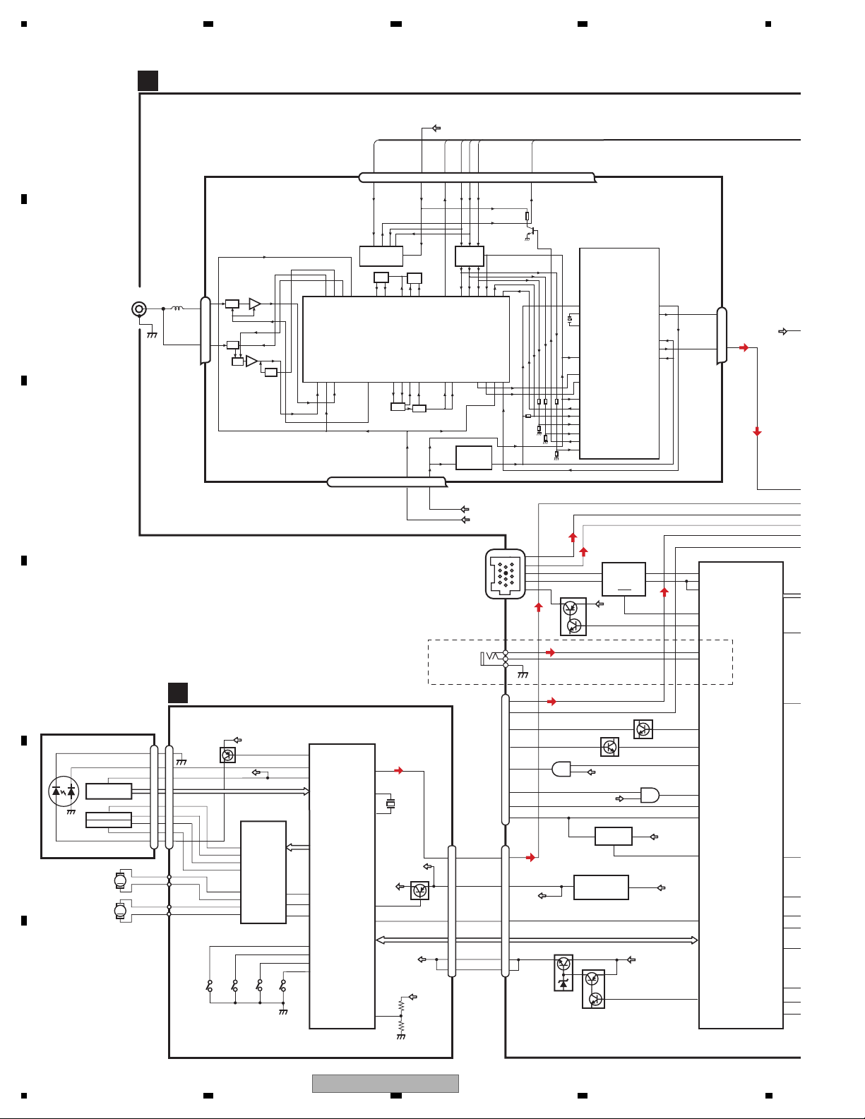
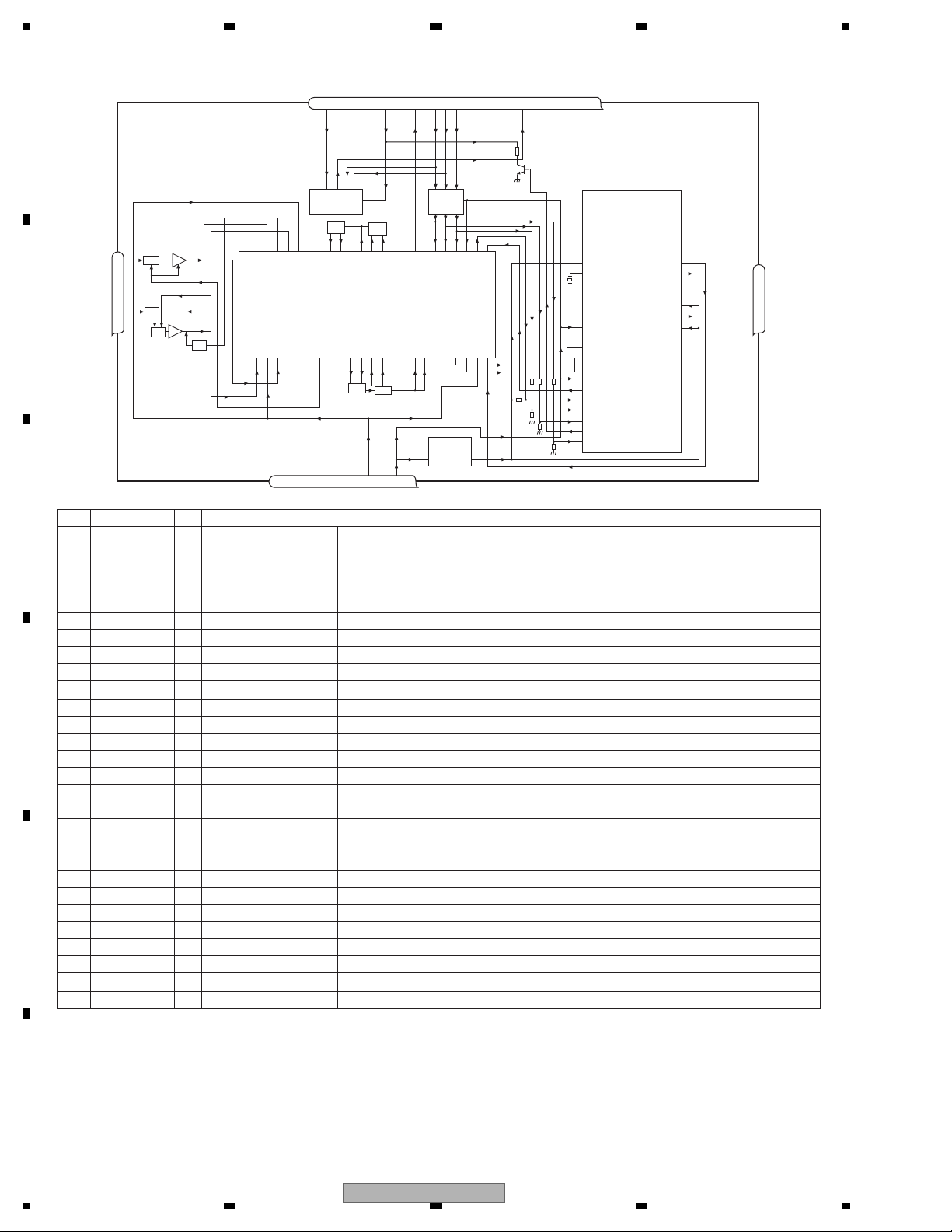
4. BLOCK DIAGRAM.......................................................................................................................................... 14
5. DIAGNOSIS.................................................................................................................................................... 18
5.1 OPERATIONAL FLOWCHART................................................................................................................ 18
5.2 ERROR CODE LIST ................................................................................................................................ 19
5.3 CONNECTOR FUNCTION DESCRIPTION............................................................................................. 21
6. SERVICE MODE ............................................................................................................................................ 22
6.1 CD TEST MODE...................................................................................................................................... 22
7. DISASSEMBLY .............................................................................................................................................. 24
8. EACH SETTING AND ADJUSTMENT ........................................................................................................... 29
8.1 CD ADJUSTMENT................................................................................................................................... 29
8.2 CHECKING THE GRATING AFTER CHANGING THE PICKUP UNIT.................................................... 30
8.3 PCL OUTPUT CONFIRMATION.............................................................................................................. 32
9. EXPLODED VIEWS AND PARTS LIST.......................................................................................................... 32
9.1 PACKING ................................................................................................................................................. 32
9.2 EXTERIOR(1) .......................................................................................................................................... 34
9.3 EXTERIOR(2) .......................................................................................................................................... 36
9.4 CD MECHANISM MODULE..................................................................................................................... 38
10. SCHEMATIC DIAGRAM............................................................................................................................... 40
10.1 OVERALL CONNECTION DIAGRAM(GUIDE PAGE) ........................................................................... 40
10.2 KEYBOARD UNIT.................................................................................................................................. 46
10.3 CD MECHANISM MODULE(GUIDE PAGE) .......................................................................................... 48
10.4 WAVEFORMS ........................................................................................................................................ 54
11. PCB CONNECTION DIAGRAM.................................................................................................................... 56
11.1 TUNER AMP UNIT................................................................................................................................. 56
11.2 KEYBOARD UNIT .................................................................................................................................. 60
11.3 CD CORE UNIT(S10.5COMP2)............................................................................................................. 62
12. ELECTRICAL PARTS LIST .......................................................................................................................... 64
E
F
4
1234
DEH-P3000IB/XS/UC
Page 5

5 678
1. SERVICE PRECAUTIONS
1.1 SERVICE PRECAUTIONS
1. You should conform to the regulations governing
the product (safety, radio and noise, and other
regulations), and should keep the safety during
servicing by following the safety instructions
described in this manual.
2. Before disassembling the unit, be sure to turn off
the power. Unplugging and plugging the connectors
during power-on mode may damage the ICs inside
the unit.
3. To protect the pickup unit from electrostatic discharge
during servicing, take an appropriate treatment
(shorting-solder) by referring to "the DISASSEMBLY".
4. After replacing the pickup unit, be sure to check the
grating.
5. Be careful in handling ICs. Some ICs such as MOS
type are so fragile that they can be damaged by
electrostatic induction.
A
B
1.2 NOTES ON SOLDERING
For environmental protection, lead-free solder is used on the printed circuit boards mounted in this unit.
Be sure to use lead-free solder and a soldering iron that can meet specifications for use with lead-free solders for repairs
accompanied by reworking of soldering.
Compared with conventional eutectic solders, lead-free solders have higher melting points, by approximately 40 C.
Therefore, for lead-free soldering, the tip temperature of a soldering iron must be set to around 373 C in general, although
the temperature depends on the heat capacity of the PC board on which reworking is required and the weight of the tip of
the soldering iron.
Compared with eutectic solders, lead-free solders have higher bond strengths but slower wetting times and higher melting
temperatures (hard to melt/easy to harden).
The following lead-free solders are available as service parts:
Parts numbers of lead-free solder:
GYP1006 1.0 in dia.
GYP1007 0.6 in dia.
GYP1008 0.3 in dia.
C
D
E
56
DEH-P3000IB/XS/UC
F
7
8
5
Page 6

1234
2. SPECIFICATIONS
2.1 SPECIFICATIONS
A
B
C
D
E
F
6
1234
DEH-P3000IB/XS/UC
Page 7

5 678
A
B
C
D
E
56
DEH-P3000IB/XS/UC
F
7
8
7
Page 8

1234
2.2 DISC/CONTENT FORMAT
A
B
C
D
E
F
8
1234
DEH-P3000IB/XS/UC
Page 9

5 678
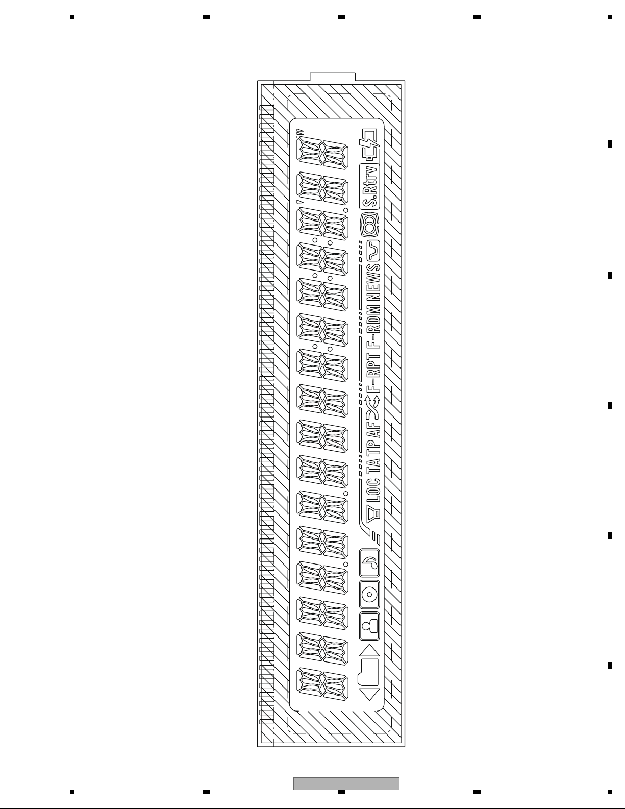
2.3 PANEL FACILITIES
A
B
C
D
E
56
DEH-P3000IB/XS/UC
F
7
8
9
Page 10

1234
A
B
C
D
E
F
10
1234
DEH-P3000IB/XS/UC
Page 11

5 678
2.4 CONNECTION DIAGRAM
A
B
C
D
E
56
DEH-P3000IB/XS/UC
F
7
8
11
Page 12
1234
3. BASIC ITEMS FOR SERVICE
3.1 CHECK POINTS AFTER SERVICING
A
To keep the product quality after servicing, please confirm following check points.
1 Confirm whether the customer complain has
been solved.
If the customer complain occurs with the
specific media, use it for the operation check.
2 CD Play back a CD.
(Track search)
3 FM/AM tuner Check FM/AM tuner action.
B
4 Check whether no disc is inside the product. The media used for the operating check must
See the table below for the items to be checked regarding audio:
C
(Seek, Preset)
Switch band to check both FM and AM.
Item to be checked regarding audio
Distortion
Noise
Volume too low
Volume too high
Volume fluctuating
Sound interrupted
demrifnocebotmetIserudecorP.oN
The customer complain must not be
reappeared.
Display, audio and operations must be
normal.
No malfunction on display, audio and
operation.
Display, audio and operations must be
normal.
be ejected.
retfaecnaraeppastinotridrosehctarcsoNkcehcecnaraeppA5
receiving it for service.
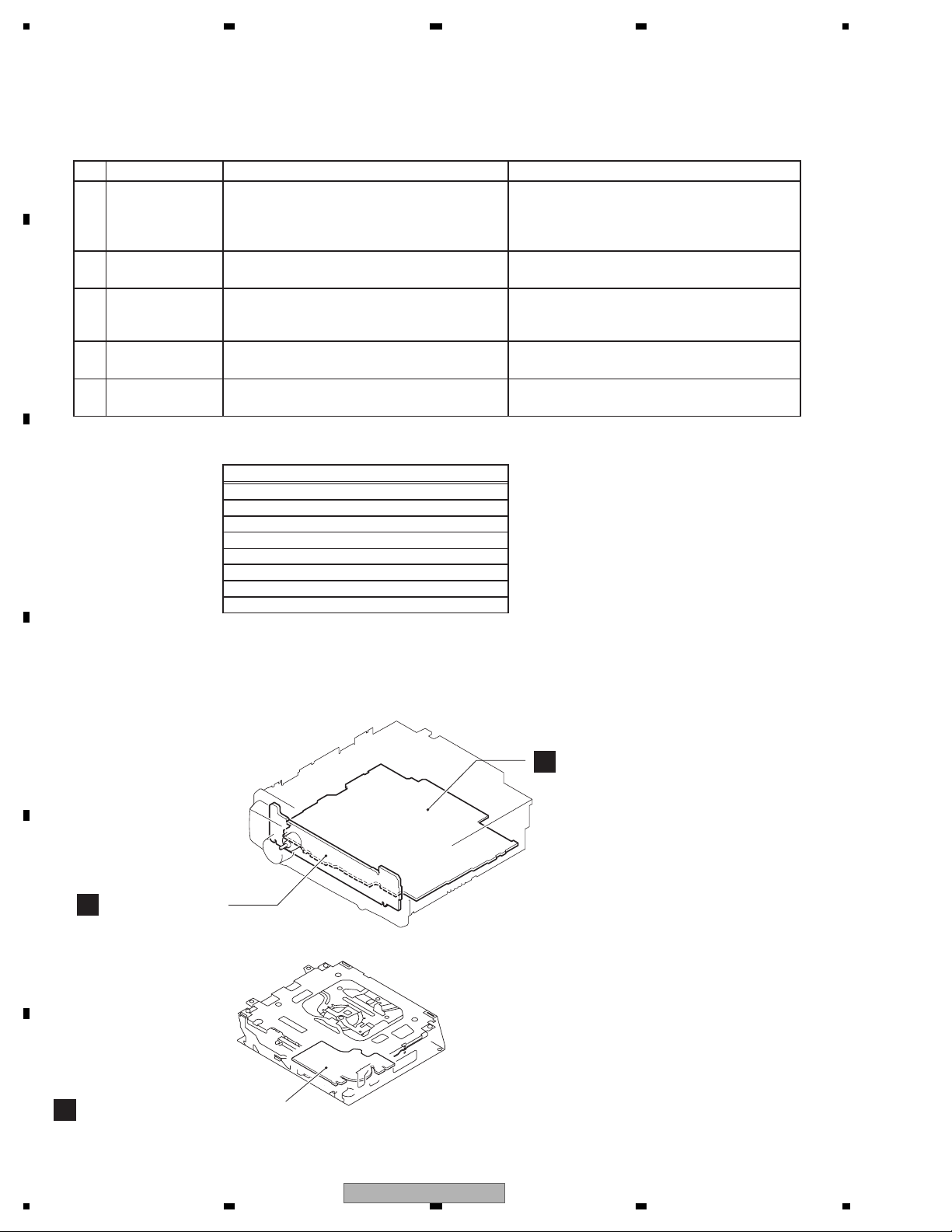
3.2 PCB LOCATIONS
D
Keyboard Unit
E
F
B
CD Core Unit (S10.5COMP2)
C
Tuner Amp Unit
A
Unit Number : CWN3104(UC)
Unit Number : CWN3106(ES)
Unit Name : Tuner Amp Unit
Unit Number : (UC)
Unit Number : (ES)
Unit Name : Keyboard Unit
Unit Number : CWX3514
Unit Name : CD Core Unit(S10.5COMP2)
12
1234
DEH-P3000IB/XS/UC
Page 13
5 678
Name
Jig
e
3.3 JIGS LIST
- Jigs List
Name
Test Disc
L.P.F.
Jig No.
No.
TCD-782
- Grease List
Name
m
Grease
Grease
Before shipping out the product, be sure to clean the
following portions by using the prescribed cleaning
tools:
Portions to be cleaned Cleaning tools
CD pickup lenses
Grease No.
rease No.
GEM1024
GEM1045
Cleaning liquid : GEM1004
Cleaning paper : GED-008
emarks
Remarks
Checking the grating
Checking the grating (Two pieces)
emarks
Remarks
CD Mechanism Module
CD Mechanism Module
A
B
C
D
E
F
56
DEH-P3000IB/XS/UC
7
8
13
Page 14
1234
D
U
4. BLOCK DIAGRAM
A
TUNER AMP UNIT
A
FM/AM TUNER UNIT
VDD5
SL
TUNPCK
TUNPDO
TUNPCE2
76 13 5 1098 11 14 18192021
NC
CE2
ROM_VDD
TUNPCE1
DI
SL
CK
CE1
TUNPDI
NC
DO
NCNCNC
NC
B
C
D
PICKUP UNIT
(P10.5)(SERVICE)
LASER
DIODE
MONITOR
E
F
DIODE
LOAD/
ANTENNA
HOLOGRAM
UNIT
FOCUS ACT.
TRACKING ACT.
SPINDLE
MOTOR
CARRIAGE
MOTOR
IC 3 EEPROM
5.0V
OSC
LPF
JA401
1
2,3
LD-
15
15
MD
5
VREF
FOM
FOP
2
TOP
1
TOM
LD+
14
14
M
M
AM ANT
1
FM ANT
3
CD CORE UNIT(S10.5COMP2)
C
ATT
ATT
ANT adj
FMRF
FMRF
RF adj
D
Q101
S905
VDD
REFO
AC,BD,F,E
CD
DRIVER
IC301
BA5839FP
12
FOM
11
FOP
14
TOP
13
TOM
16
SOP
LOEJ
15
SOM
18
CLCONT
LCOP
17
CONT
LCOM
8EJ
S903
DSCSNS
CN101
5
88
33
2
1
44
FOM
FOP
TOP
TOM
S904
12EJ
RFGND
OSCGND
212 1522 16 4 17
RF-AMP, CD DECODER,
MP3/WMA DECODER,
DIGITAL SERVO /
DATA PROCESSOR
141
LD
142
PD
133
REFOUT
IC201
TD,FD
PE5547A
SD,MD
22
5
LOEJ
21
43
CLCONT
9
41
CONT
8
12EJ
7
8EJ
6
DSCSNS
9
HOME
S901
HOME
VDSENS
LOUT
XTAL
/XTAL
/PUEN
/RESET
MIXER, IF AMP
DGND
AUDIOGNDNCVCC
55
50
52
39
16
11
IC 1
3.3V
T51
LOUT
X201
16.93MHz
VDD
VCC
BRST,BRXEN,BSRQ
BDATA,BSCK
VD
CF52
Q102
VD
IC 5
5V t 3.3V
IC 4
3.3V t 2.5V
3.3V
VDD_3.3
3.3V
VCC8
IP-BUS
WIRED
REMOTE
DEH-P3000IB/XS/UC
Only
iPod
ADAPTER
CN701
13
VDD
9
/RESET
8
VD
2
1
JA621
Rch
30
29
21
54
40
34
94
83
85
31
32
86
87
84
24
Lch
23
TX
RX
CONTROLLER
RX2
IC601(2/2)
PEG410B8
IPPW
ASENBO
KEYD
KEYAD
PID
PSENS
TXPOD
RXPOD
PSENSG
PVSENS
PPOWER
SYSTEM
IC 2
2.5V
DET, FM MPX
2.5V
CDL
JA101
BUSL+
7
BUSL-
11
5
1
8
Q101
IP-BUS DRIVER
BUS-
5
BUS+
6
IC101
HA12241FP
BUS-
DIN1
BUS+ ROUT
STBY
8
B.UP
IPPW
TX
1
RX
2
Q102
3
KEYD
2
KEYAD
1
JA561
AUDIO-L
5
iPodAG
13
4
10
3
6
11
2
3
ACC-ID
ACC-PW
TX-iPod
RX-iPod
iPodGND
F/W-PWR
CN701
LOUT
TX
→
5.5V 3.3V
IC591
TC7SET08FUS1
1
4
2
Q567
VDD3.3
VDD5
Q561-564
Q566
RX
→
3.3V 5.5V
IC592
TC7SET08FUS1
1
2
B.UP
4
VDD 3.3V REGULATOR
IC702
7
VDD3.3
RESET
8
BRST,BRXEN,BSRQ,BDATA,BSCK
VD
14
15
3
NJM2885DL1-33
CDRST
VD 7.6V REGULATOR
Q702
Q701
1
VDD5
23
VDRST
B.UP
22
VDCONT
VDD5
MUTE
SYSPW
ILMPW
SWVDD
ROT0
DPDT
KYDT
DSENS
TUNERL
CDL
BUSL+
BUSL-
iPodL
iPodAG
ROT1
JOY
2
41
48
B.
51
VD
49
4
3
82
35
36
11
14
1234
DEH-P3000IB/XS/UC
Page 15
5 678
A
Rch
24
Lch
23
TX
RX
SYSTEM
CONTROLLER
RX2
IC601(2/2)
PEG410B8
IPPW
ASENBO
KEYD
KEYAD
VDD5
MUTE
SYSPW
TUNERL
CDL
BUSL+
BUSL-
iPodL
iPodAG
2
S-80835CNMC-B8U
41
48
RESET
IC961
AUXL
TUNPCE2
TUNPCE1
TUNPDI
TUNPDO
TUNPCK
SL
65
66
68
69
67
97
1
12
ELECTRONIC VOLUME/
6
7
3
4
2
1
5
VST,VCK,VDT
TUNPCE2
TUNPCE1
TUNPDI
TUNPDO
TUNPCK
SL
SYSTEM
CONTROLLER
IC 601(1/2)
PEG410B8
RESET
DALMON
SOURCE SELECTOR
IN2_L
IN1_L
IC151
PML018A
IN4+_L
IN4-_L
IN5+_L
IN5-_L
IN3_L
BSENS
ASENS
Front_L
Rear_L
FL
MUTE
JA351
RCFL
4
Q351
RCRL
JA901
B.UP
ACC
8
16
14
RCA OUT
B
B.UP
ACC
BZ601
BUZZER
26
PEE
15
Xin
X601
10MHz
13
Xout
47
18
75
RL
VDD5 REGULATOR
VDD5
BACKUP SENSE
Q911
Q912
B.UP
Q352
Q931
ACC SENSE
GND
FL-
FL+
RL-
RL+
C
BREM
BREM
15
FL-
7
FL+
5
RL-
8
RL+
6
11
POWER AMP
10
11
MUTE
Q453
14
12
FLIN
RLIN
22 4
IC301
PAL007C
STBYMUTE
VCC
B.REM
25
B.UP
6,20
23
FL-
21
FL+
3
RL-
5
RL+
B.UP
MUTE
Q451
3.3V REGULATOR
IC401
13
3.3V
NJM2885DL1-33
VCC8
SYSPW
VCC8
VCC8 REGULATOR
2
IC921
NJM2388F84
4
1
B.UP
D
PID
PSENS
TXPOD
RXPOD
PSENSG
PVSENS
PPOWER
VDRST
VDCONT
ILMPW
SWVDD
ROT0
ROT1
DPDT
KYDT
DSENS
1
OUT1
AUX IN
IC751
NJM2794V
IN1+
IN1-
13
11
ILM+B
Q841
B.UP
Q842
51
VDD5
49
4
3
82
JOY
35
36
11
Q851
SWVDD
Q852
CN803
AUXL
AUXGND
ILM+B ILM
SWVDD
ROT0
ROT1
JOY
DPDT
KYDT
DSENS
56
B
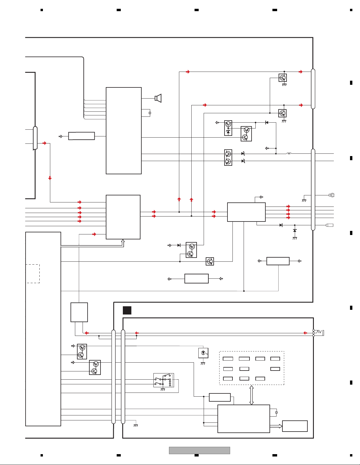
KEYBOARD UNIT
JA1
CN1
AUXL
13
13
AGND
10
10
12
12
9
9
SWVDD
3
3
ROTARY COMMANDER
Phase_B
ROT0
8
8
Phase_A
ROT1
7
7
JOY
4
4
DPDT
5
5
KYDT
6
6
DSENS
2
2
S28
10
1
DEH-P3000IB/XS/UC
ILLUMI
REM.CON.
3
GP1UX51RK
50
49
46
47
IC2
DPDT
KYDT
V3
VDD
EJECT
CLOCK
S1
SOURCE
S5 S6
DISP
S8
RPT
SW
1
57
REM
LCD DRIVER/
KEY CONTROLLER
IC1
PD6538A
7
KEY MATRIX
S2
S9
KST1-4
KDT1-3
KEY DATA
S3 S4
LIST
S10
IPOD
X0
X1
BAND
S7
RDM
54
X1
5MHz
55
LCD
V1
3
2
1
8
FRONT_AUX
E
F
15
Page 16
1234
- FM/AM Tuner Unit
A
7 6 13 5 10 9 8 11 14 18 19 20 21
NC
CE2
ROM_VDD
DI
SL
CK
CE1
NC
DO
NCNCNC
NC
3.3 V
IC 5
5 V 3.3 V
t
IC 4
t
3.3 V 2.5 V
2.5 V
IC 2
2.5 V
DET, FM MPX
AM ANT
1
AT T
FM ANT
3
B
C
No. Symbol I/O Explain
AT T
ANT adj
FMRF
FMRF
RF adj
IC 3 EEPROM
5.0 V
OSC
LPF
IC 1
3.3 V
MIXER, IF AM P
T51
CF52
RFGND
OSCGND
DGND
212 1522 16 4 17
AUDIOGNDNCVCC
VDD_3.3
1 AMANT I AM antenna input AM antenna input high impedance AMANT pin is connected with
an all antenna by way of 4.7 µH. (LAU type inductor) A series circuit
including an inductor and a resistor is connected with RF ground for
the countermeasure against the hum of power transmission line.
2 RFGND RF ground Ground of antenna block
3 FMANT I FM antenna input Input of FM antenna 75 Surge absorber
(DSP-201M-S00B) is necessary.
4 VCC power supply The power supply for analog block. D.C 8.4 V ± 0.3 V
5 SL O signal level Output of FM/AM signals level
6 CE2 I chip enable-2 Chip enable for EEPROM ”Low” active
7 NC non connection Not used
D
8 CE1 I chip enable-1 Chip enable for AF•RF ”High” active
9 CK I clock Clock
10 DI I data in Data input
11 NC non connection Not used
12 OSCGND osc ground Ground of oscillator block
13 ROM_VDD power supply Power supply for EEPROM pin 13 is connected with a power supply of
micro computer.
14 DO O data out Data output
15 DGND digital ground Ground of digital block
16 NC non connection Not used
17 VDD_3.3 power supply The power supply for digital block. 3.3 V ± 0.2 V
18 NC non connection Not used
19 NC non connection Not used
E
20 NC non connection Not used
21 NC non connection Not used
22 AUDIOGND audio ground Ground of audio block
23 L ch O L channel output FM stereo “L-ch” signal output or AM audio output
24 R ch O R channel output FM stereo “R-ch” signal output or AM audio output
Rch
24
Lch
23
F
16
1234
DEH-P3000IB/XS/UC
Page 17
- YAW5094
5 678
A
B
C
D
E
56
DEH-P3000IB/XS/UC
F
7
8
17
Page 18
1234
crocompute
5. DIAGNOSIS
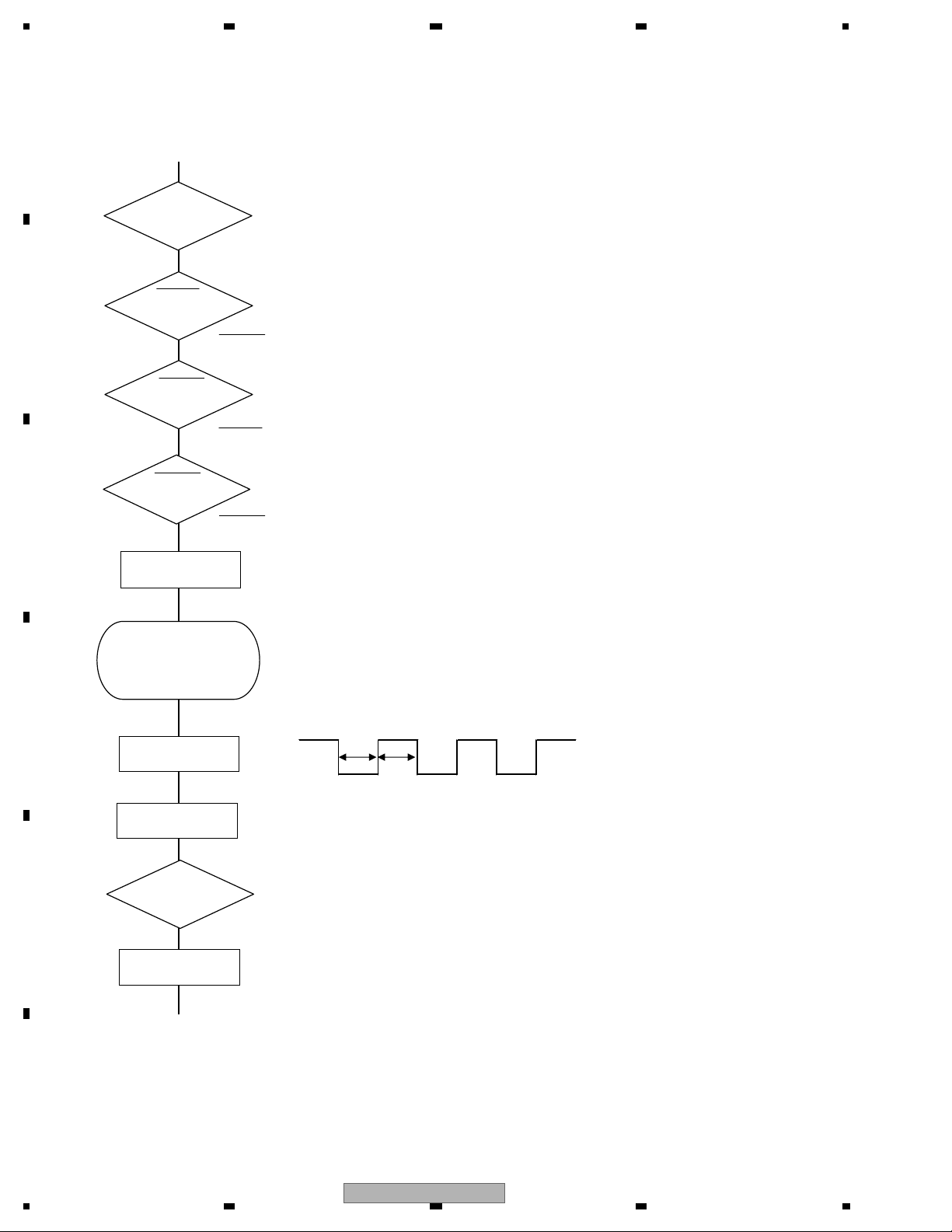
5.1 OPERATIONAL FLOWCHART
A
Power ON
Vcc = 5 V
Pin 16
BSENS
B
Pin 18
BSENS = L
ASENS
Pin 75
ASENS = L
DSENS
Pin 11
C
DSENS = L
ASENBO <- H
Pin 40
Starts
communication
with Grille
mi
D
r.
300 ms
SWVDD <- H
Pin 49
300 ms
Source keys
operative
In case of the above signal, the communication
with Grille microcomputer may fail
If the time interval is not 300 msec, the oscillator
may be defective.
Source ON
E
F
18
SYSPW <- H
Pin 48
Completes power-on operation.
(After that, proceed to each source
operation)
DEH-P3000IB/XS/UC
1234
Page 19
5 678
5.2 ERROR CODE LIST
- Error Messages
If a CD is not operative or stopped during operation due to an error, the error mode is turned on and cause(s) of
the error is indicated with a corresponding number. This arrangement is intended at reducing nonsense calls from
the users and also for facilitating trouble analysis and repair work in servicing.
(1) Basic Indication Method
1) When SERRORM is selected for the CSMOD (CD mode area for the system), error codes are written to DMIN
(minutes display area) and DSEC (seconds display area). The same data is written to DMIN and DSEC. DTNO
remains in blank as before.
A
2) Head unit display examples
Depending on display capability of LCD used, display will vary as shown below. xx contains the error number.
8-digit display 6-digit display 4-digit display
ERROR-xx ERR-xx E-xx
(2) Error Code List
Code
10
Class Displayed error code Description of the code and potential cause(s)
Electricity Carriage Home NG CRG can't be moved to inner diameter.
SERVO LSI Com-
CRG can't be moved from inner diameter.
munication Error → Failure on home switch or CRG move mechanism.
Communication error between microcomputer and SERVO LSI.
11 Electricity Focus Servo NG Focusing not available.
→ Stains on rear side of disc or excessive vibrations on REWRITABLE.
12 Electricity Spindle Lock NG Spindle not locked. Sub-code is strange (not readable).
Subcode NG → Failure on spindle, stains or damages on disc, or excessive vibrations.
A disc not containing CD-R data is found.
Turned over disc are found, though rarely.
CD signal error.
17 Electricity Setup NG AGC protection doesn't work. Focus can be easily lost.
→ Damages or stains on disc, or excessive vibrations on REWRITABLE.
30 Electricity Search Time Out Failed to reach target address.
→ CRG tracking error or damages on disc.
44 Electricity ALL Skip Skip setting for all track.
(CD-R/RW)
50
Mechanism
CD On Mech Error Mechanical error during CD ON.
→ Defective loading motor, mechanical lock and mechanical sensor.
A0 System Power Supply NG Power (VD) is ground faulted.
→ Failure on SW transistor or power supply (failure on connector).
Remarks: Mechanical errors are not displayed (because a CD is turned off in these errors).
Unreadable TOC does not constitute an error. An intended operation continues in this case.
Upper digits of an error code are subdivided as shown below:
1x: Setup relevant errors, 3x: Search relevant errors, Ax: Other errors.
B
C
D
E
56
DEH-P3000IB/XS/UC
F
7
8
19
Page 20

1234
iPod error
A
ActionCauseMessage
Transfer the songs to the iPod.No songs in the iPodNO SONGS
STOP
No songs in the current list
Select a list that contains the songs.
Disconnect the cable from the iPod. Once the iPod
ERROR-11
Communication failure
main menu is displayed, connect the cable again.
Reset the iPod.
ERROR-21
Old version of the iPod
Update the iPod version.
Reset the iPod.iPod failureERROR-30
B
ERROR-A0
iPod is not charged but operates
correctly.
Check if the connection cable for the iPod shorted out.
After checking, switch the ignition key or disconnect the
iPod and connect again.
C
D
E
F
20
1234
DEH-P3000IB/XS/UC
Page 21
5 678
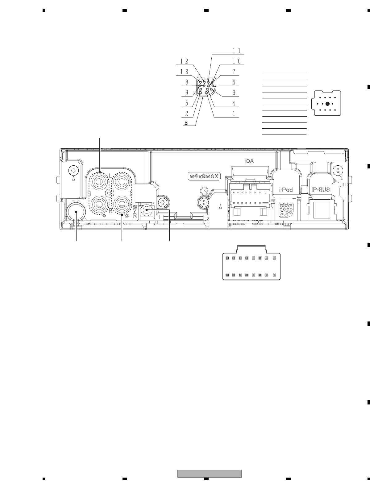
5.3 CONNECTOR FUNCTION DESCRIPTION
REAR
OUTPUT
1 F/W-GND
2 F/W-PWR
3 TX-iPod
4 ACC-ID
5 AUDIO-L
6 RX-iPod
7 NC
8 AUDIO-R
9 iGND
10 ACC-PW
11 iPodGND
12 NC
13 iPodAG
RT1 GND
RT2 GND
iPod
1. BUS+
2. GND
3. GND
4. NC
5. BUS-
6. GND
7. BUS L+
8. ASENB
9. BUS R+
10. BUS R-
11. BUS L-
A
IP-BUS INPUT
111098
765
4321
B
C
ANTENNA
FRONT
OUTPUT
WIRED REMOTE
INPUT(UC)
3
1
4
2
1 FR+
2 RR+
3 FR4 RR5 FL+
6 RL+
7 FL8 RL-
9
7
5
8
6
10
13 15
11
14 16
12
9 NC
D
10 NC
11 B.REM
12 NC
13 NC
14 ACC
15 GND
16 B.UP
E
56
DEH-P3000IB/XS/UC
F
7
8
21
Page 22

1234
6. SERVICE MODE
6.1 CD TEST MODE
A
During pressing the "SOURCE" and "RPT" keys simultaneously, perform the reset-start, then turn ON
the CD to enter the CDS test mode.
• How to issue the 1 - 6 keys in the 08 model's slave test:
The specification of the 08 model does not include the 1 - 6 keys issuance function for H/U and the remote control unit.
Therefore, in order to issue commands in a slave test, use the direct FUNCTION keys alternatively to enable the equal
key command sending function to the existing models.
Outline) Use the direct FUNCTION keys to display, select, or issue the KEY 1 - 6.
B
<Direct FUNCTION keys and corresponding functions>
Direct FUNCTION key Normal mode Slave test mode
A Selecting a key command
B
C Switching a screen
SAT
RDM Issuing a key command
RPT
• For convenience, a name of each direct FUNCTION key is shown as "A", "B", and "C".
• How to issue the 1 - 6 keys for the CDS source:
(The areas below are overwritten and displayed on character strings for the normal mode display.)
C
1 During the slave test mode, the key name "K1" is shown at the left by default.
In this condition, press the A key to toggle K1 - K6, and select a command to be sent to the slave.
COMPACT D I SC
K1 ! T -!! !!!!
• The one-line model shows only the bottom
column.
DNOCESETUNIMKRTREDLOF
A key
COMPACT D I SC
D
K6 T
! -!! !!!!
2 During the K1 - K6 key names are displayed, press the B key and issue the selected command.
COMPACT D I SC
K1 T
! -!! !!!!
Send a key command selected
by pressing the KEY 1.
B key
E
3 Press the C key to change display/non-display of key names.
When the non-display mode is selected for the K1 - K6 key names, "A key" and "B key" are invalid.
COMPACT D I SC
K1 T
! -!! !!!!
C key
COMPACT D I SC
F -! T
F
22
1234
! -!! !!!!
DEH-P3000IB/XS/UC
• Pressing the A key or B key does not work.
Page 23

5 678
- Flow Chart
[Key]
Contents
Display
[BAND]
Power Off
TRK MIN SEC
[BAND]
Power Off
TRK MIN SEC
[BAND]
Power Off
TRK MIN SEC
[SOURCE] + [RPT] +
BU + ACC
Test Mode In
[CD] or [SOURCE]
Source On
TRK MIN SEC
[BAND]
Power On
(T.Offset is adjusted)
TRK MIN SEC
00 00 00
[3]
Focus Close
S curve check
TRK MIN SEC
91 91 91
[1]
T.Close & AGC
Applicable servomechanism
TRK MIN SEC
?tr ?min ?sec
[1]
F,T,RF AGC
F.Bias display switching
*7
TRK MIN SEC
[3]
Power On
(T.Offset is not adjusted)
TRK MIN SEC
99 99 99
[6]
Focus Mode switching
[6] [3]
Applicable servomechanism
[3] [6]
TRK MIN SEC
0X 0X 0X
TRK MIN SEC
?tr ?min ?sec
F,T AGC / F.Bias
RF AGC
TRK MIN SEC
?tr ?min ?sec
*2
[2]
TRK MIN SEC
GG GG GG
[1]
RF AGC coefficient display
TRK MIN SEC
TRK MIN SEC
?tr ?min ?sec
RF AMP
Gain switching
Tracking Servo
Close
00 00 00
or 99 99 99
RF AGC /
?? ?? ??
CRG/TR jump
value switching
*1
*5
[4]
SPINDLE
Speed switching
TRK MIN SEC
SP SP SP
[>]
CRG +
00 00 00
or 99 99 99
[>]
CRG +
8X 8X 8X
or 9X 9X 9X
[>]
CRG/TR Jump +
TRK MIN SEC
?tr ?min ?sec
*9
[<]
CRG -
00 00 00
or 99 99 99
[<]
CRG -T.Close
8X 8X 8X
or 9X 9X 9X
[<]
*4 *4
CRG/TR Jump -
TRK MIN SEC
?tr ?min ?sec?? ?? ??
*8
*6
[2]
Self-adjusting
switching
*3*8
TRK MIN SEC
?? ?? ??
[2]
T.Balance adjustment /
T.BAL coefficient display
TRK MIN SEC
?? ?? ??
[2]
Tracking Open
8X 8X 8X
or 9X 9X 9X
[5]
Gop Mode
Gop Mode switching
TRK MIN SEC
OL OL OL
*10
A
B
C
[BAND]
Power Off
TRK MIN SEC
*1) TYP → + 6 dB → + 12 dB
TRK
*2) Focus Close
TRK00MIN00SEC
TRK99MIN99SEC
(
MIN
SEC
TRK06MIN06SEC
→ S Curve check setting → F EQ measurement setting
00
TRK
MIN01SEC
01
01
06
TRK12MIN12SEC
TRK02MIN02SEC
99)
12
02
*3) F.Offset Display → RF.Offset → T.Offset Display → Switch to the
order of the original display
*4) 1TR/4TR/10TR/32TR/100TR
*5) Single
→ 4TR → 10TR → 32TR → 100TR → CRG Move
9x(8x):91(81) 92(82) 93(83) 94(84) 95(85) 96(86)
*6) Only at the time of CRG move, 100TR jump
*7) TRK/MIN/SEC
→ F.AGC → T.AGC Gain → F.Bias → RF AGC
*8) CRG motor voltage = 2 [V]
*9) TYP (1X)
TRK
MIN
→ 2X → 1X
SEC
TRK
MIN22SEC
22
22
TRK11MIN11SEC
11
[2]
Tracking Open
8X 8X 8X
or 9X 9X 9X
Operation
[Key]
Test Mode
[BAND] Power On/Off
[>]
CRG + / TR Jump +
(Direction of the external surface)
[<]
CRG - / TR Jump (Direction of the internal surface)
[1] T. CLS & AGC & Applicable servomechanism /
AGC,AGC display setting
[2] RF Gain switching / Offset adjustment display /
T.Balance adjustment / T. Open
[3] F. Close,S Curve / Rough Servo and RF AGC /
F,T,RF AGC
[4]
SPDL 1X/2X switching
As for the double speed(2x), audio output cannot be
supported.
[5]
Error Rate measurement
ON : ERR 30Counts Start
BER display data[%]
[6] F. Mode switching / Tracking Close / CRG•TR
Jump Switching
*10) OFF(TYP)
TRK
MIN
→ FORCUS → TRACKING
SEC
TRK
MIN70SEC
70
70
TRK71MIN71SEC
D
E
71
• As for the double speed (2x), audio output cannot be supported
*) • After the [Eject] key is pressed keys other than the [Eject] key should not be pressed, until disc ejection is complete.
• When the key [2] or [3] is pressed during the Focus Search, the power supply should be immediately turned off (otherwise the lens
sticks to Wall, causing the actuator to be damaged).
• In the case of TR jump other than to 100TR, the function shall continue to be processed even if the TR jump key is released. As for
the CRG Move and 100TR Jump, the mechanism shall be set to the Tracking Close mode when the key is released.
• When the power is turned on/off the jump mode is reset to the Single TR (91) while the gain of the RFAMP is reset to 0 dB. At the
same time all the self-adjusting values shall return to the default setting.
56
DEH-P3000IB/XS/UC
7
8
F
23
Page 24

1234
7. DISASSEMBLY
-
A
Removing the Keyboard Unit (Fig.1)
Remove the four screws.
1
Remove the Cover
and then remove the Keyboard Unit.
B
-
Removing the Holder (Fig.2)
Take off the pick of left and right
and then a holder slide to the arrow course.
C
Removing the Case and Panel (Fig.3,4)
-
Remove the Case.(Fig.3)
1
1
Holder
Cover
1
1
Fig.1
Pick
Fig.2
Case
D
Take off four picks of the part of the arrow
and then remove the Panel.(Fig.4)
E
F
Fig.3
Panel
Fig.4
24
1234
DEH-P3000IB/XS/UC
Page 25

5 678
-
Removing the Panel Assy(Fig.5,6)
Push the place of the arrows
and then remove Panel Assy.
A
Fig.5
Panel Assy
B
Fig.6
-
Removing the CD Mechanism Module (Fig.7)
Remove the four screws.
1
Disconnect the cable
and then remove the CD Mechanism Module.
C
1
1
1
D
1
Fig.7
CD Mechanism Module
E
56
DEH-P3000IB/XS/UC
F
7
8
25
Page 26

1234
-
Removing the Tuner Amp Unit(Fig.8,9)
A
Remove the two screws.(Fig.8)
1
Remove the screw.(Fig.8)
2
2
1
Straighten the tabs at four locations
3
indicated.(Fig.9)
Remove the screw and then remove
4
B
the Tuner Amp Unit.(Fig.9)
Tuner Amp Unit
3
3
3
1
Fig.8
4
3
C
Fig.9
D
E
F
26
1234
DEH-P3000IB/XS/UC
Page 27

5 678
- How to hold the Mechanism Unit
1. Hold the Upper and Lower Frames.
2. Do not hold the front portion of the Upper
Frame, because it is not very solid.
A
B
Do not squeeze this area.
- Removing the Upper and Lower Frames
1. With a disc inserted and clamped in the
mechanism, remove the two Springs (A), the
six Springs (B), and the four Screws.
2. Turn the Upper Frame using the part "a" as
a pivot, and remove the Upper Frame.
3. While lifting the Carriage Mechanism,
remove it from the three Dampers.
Caution: When assembling, be sure to apply
some alcohol to the Dampers and assemble
the mechanism in a clamped state.
B
A
Damper
Carriage Mechanism
B
B
A
Lower Frame
a
Upper Frame
C
B
B
B
Damper
D
56
DEH-P3000IB/XS/UC
E
F
7
8
27
Page 28

1234
- How to remove the CD Core Unit
1. Apply Shorting Solder to the flexible cable of
the Pickup, and disconnect it from the
A
connector.
2. Unsolder the four leads, and loosen the
Screw.
3. Remove the CD Core Unit.
Caution: When assembling the CD Core Unit,
assemble it with the SW in a clamped state
so as not to damage it.
B
CD Core Unit
Shorting Solder
Screw
Solder
- How to remove the Pickup Unit
1. Make the system in the carriage mechanism mode, and have it clamped.
2. Remove the CD Core Unit and remove the leads from the Inner Holder.
3. Remove the Poly Washer, Change Arm, and Pickup Lock Arm.
C
4. While releasing from the hook of the Inner Holder, lift the end of the Feed Screw.
Caution: When assembling, move the Planet Gear to the load/eject position before setting the Feed Screw in the Inner
Holder.
Assemble the sub unit side of the Pickup, taking the plate (Chassis) in-between. When treating the leads of the Load
Carriage Motor Assy, do not make them loose over the Feed Screw.
Poly Washer
Pickup Lock Arm
Feed Screw
D
E
Change Arm
Inner Holder
Planet Gear
Pickup Rack
Chassis
Pickup
F
28
1234
DEH-P3000IB/XS/UC
Page 29

5 678
8. EACH SETTING AND ADJUSTMENT
8.1 CD ADJUSTMENT
A
1) Cautions on adjustments
In this product the single voltage (3.3 V) is used for the
regulator. The reference voltage is the REFO1 (1.65 V)
instead of the GND.
If you should mistakenly short the REFO1 with the GND
during adjustment, accurate voltage will not be obtained,
and the servo’s misoperation will apply excessive shock
to the pickup. To avoid such problems:
a. Do not mix up the REFO1 with the GND when
connecting the (-) probe of measuring instruments.
Especially on an oscilloscope, avoid connecting the (-)
probe for CH1 to the GND.
b. In many cases, measuring instruments have the same
potential as that for the (-) probe. Be sure to set the
measuring instruments to the floating state.
c. If you have mistakenly connected the REFO1 to the GND,
turn off the regulator or the power immediately.
Before mounting and removing filters or leads for
adjustment, be sure to turn off the regulator.
For stable circuit operation, keep the mechanism
operating for about one minute or more after the
regulator is turned on.
In the test mode, any software protections will not
work. Avoid applying any mechanical or electrical
shock to the mechanism during adjustment.
2) Test mode
This mode is used to adjust the CD mechanism module.
To enter the test mode.
While pressing the 4 and 6 keys at the same time, reset.
To exit from the test mode.
Turn off the ACC and back up.
Notes:
a. During ejection, do not press any other keys than the
EJECT key until the loaded disc is ejected.
b. If you have pressed the (→) key or (←) key during focus
search, turn off the power immediately to protect the
actuator from damage caused by the lens stuck.
c. For the TR jump modes except 100TR, the track jump
operation will continue even if the key is released.
d. For the CRG move and 100TR jump modes, the tracking
loop will be closed at the same time when the key is
released.
e. When the power is turned off and on, the jump mode
is reset to the single TR (91), the RF amp gain is set to 0 dB,
and the auto-adjustment values are reset to the default
settings.
B
C
The RFI and RFO signals with a wide frequency range
are easy to oscillate. When observing the signals,
insert a resistor of 1k ohms in series.
The load and eject operation is not guarantied with the
mechanism upside down. If the mechanism is blocked
due to mistaken eject operation, reset the product or
turn off and on the ACC to restore it.
D
E
56
DEH-P3000IB/XS/UC
F
7
8
29
Page 30

1234
8.2 CHECKING THE GRATING AFTER CHANGING THE PICKUP UNIT
A
Note :
The grating angle of the PU unit cannot be adjusted after the PU unit is changed. The PU unit in the CD mechanism
module is adjusted on the production line to match the CD mechanism module and is thus the best adjusted PU
unit for the CD mechanism module. Changing the PU unit is thus best considered as a last resort. However, if the
PU unit must be changed, the grating should be checked using the procedure below.
Purpose :
To check that the grating is within an acceptable range when the PU unit is changed.
B
Symptoms of Mal-adjustment :
If the grating is off by a large amount symptoms such as being unable to close tracking, being unable to perform
track search operations, or taking a long time for track searching.
Method :
Measuring Equipment
Measuring Points
Oscilloscope, Two L.P.F.
E, F, REFO1
Disc TCD-782
Mode TEST MODE
CD CORE UNIT(S10.5COMP2)
C
D
REFO1
FE
VREF
VREF
E
F
L.P.F.
100 kohm
100 kohm
L.P.F.
390 pF
390 pF
Xch Ych
Oscilloscope
Checking Procedure
1. In test mode, load the disc and switch the 3 V regulator on.
2. Using the → and ← buttons, move the PU unit to the innermost track.
3. Press key 3 to close focus, the display should read "91". Press key 2 to implement the tracking balance
adjustment the display should now read "81". Press key 3. The display will change, returning to "81" on the
fourth press.
E
4. As shown in the diagram above, monitor the LPF outputs using the oscilloscope and check that the phase
difference is within 75 degrees. Refer to the photographs supplied to determine the phase angle.
5. If the phase difference is determined to be greater than 75 degrees try changing the PU unit to see if there is any
improvement. If, after trying this a number of times, the grating angle does not become less than 75 degrees then the
mechanism should be judged to be at fault.
Note
Because of eccentricity in the disc and a slight misalignment of the clamping center the grating waveform may be
seen to "wobble" ( the phase difference changes as the disc rotates). The angle specified above indicates the
average angle.
Hint
Reloading the disc changes the clamp position and may decrease the "wobble".
F
30
1234
DEH-P3000IB/XS/UC
Page 31

5 678
Grating waveform
0 degrees
45 degrees
Ech → Xch 20 mV/div, AC
Fch → Ych 20 mV/div, AC
A
30 degrees
B
60 degrees
C
75 degrees
D
90 degrees
E
F
56
DEH-P3000IB/XS/UC
7
8
31
Page 32

1234
N
8.3 PCL OUTPUT CONFIRMATION
A
- PCL output
In the normal operation mode (with the detachable panel installed, the ACC switched ON, the standby mode
cancelled), shift the TESTIN IC601(Pin 63) terminal to H.
The clock signal is output from the PCL terminal IC601(Pin 39).
The frequency of the clock signal is 625 000 Hz that is one 32th of the fundamental frequency.
9. EXPLODED VIEWS AND PARTS LIST
OTES : Parts marked by " * " are generally unavailable because they are not in our Master Spare Parts List.
B
The > mark found on some component parts indicates the importance of the safety factor of the part.
Therefore, when replacing, be sure to use parts of identical designation.
Screw adjacent to mark on the product are used for disassembly.
For the applying amount of lubricants or glue, follow the instructions in this manual.
(In the case of no amount instructions,apply as you think it appropriate.)
9.1 PACKING
""
C
D
E
F
32
1234
DEH-P3000IB/XS/UC
Page 33

5 678
(1) PACKING SECTION PARTS LIST
No. Description Part No.
Mark No. Description Part No.
1 Cord Assy CDP1017
2 Accessory Assy See Contrast table(2)
3 Screw See Contrast table(2)
4 Screw Assy CEA3849
5 Screw CBA1650
* 6 Polyethylene Bag CEG-127
7 Screw CRZ50P090FTC
8 Screw TRZ50P080FTC
9 Polyethylene Bag CEG1160
10 Handle CND3707
11 Bush CNV3930
12 Polyethylene Bag See Contrast table(2)
* 13 Battery CEX1065
Mark
14 Remote Control Assy CXC8885
15 Unit Box See Contrast table(2)
16 Contain Box See Contrast table(2)
17 Protector See Contrast table(2)
18 Protector See Contrast table(2)
* 19-1 Warranty Card See Contrast table(2)
19-2 Owner's Manual See Contrast table(2)
19-3 Installation Manual See Contrast table(2)
19-4 Caution Card CRP1310
19-5 Caution Card See Contrast table(2)
19-6 Owner's Manual See Contrast table(2)
20 Case Assy See Contrast table(2)
(2) CONTRAST TABLE
DEH-P3000IB/XS/UC and DEH-P3000IB/XS/ES are constructed the same except for the following:
Mark No. Description DEH-P3000IB/XS/UC DEH-P3000IB/XS/ES
2 Accessory Assy * CEA6707 CEA6708
3 Screw BPZ20P080FTC Not used
12 Polyethylene Bag CEG1374 CEG1373
15 Unit Box CHG6373 CHG6372
16 Contain Box CHL6373 CHL6372
A
B
C
17 Protector YHP5041 YHP5039
18 Protector YHP5042 YHP5040
* 19-1 Warranty Card CRY1246 Not used
19-2 Owner's Manual CRD4245 CRD4247
19-3 Installation Manual CRD4246 CRD4249
19-5 Caution Card CRP1294 Not used
19-6 Owner's Manual Not used CRD4248
20 Case Assy Not used YXB5009
Owner's Manual,Installation Manual
Part No. Language
CRD4245 English, French
CRD4246 English, French
CRD4247 English, Spanish, Portuguese(B)
CRD4248 Traditional Chinese, Arabic
CRD4249 English, Spanish, Portuguese(B), Traditional Chinese, Arabic
D
E
56
DEH-P3000IB/XS/UC
F
7
8
33
Page 34

1234
9.2 EXTERIOR(1)
A
B
A
B
C
A
D
A
B
E
F
34
1234
DEH-P3000IB/XS/UC
Page 35

5 678
(1) EXTERIOR(1) SECTION PARTS LIST
Mark No. Description Part No.
1 Screw See Contrast table(2)
2 Screw BSZ26P060FTC
3 Screw BSZ30P060FTC
4 Screw BSZ30P100FTC
5 Screw BSZ30P200FTC
6 Cable CDE8336
7 Earth Plate CNC8915
8 Cushion CNM8890
9 Holder See Contrast table(2)
10 Tuner Amp Unit See Contrast table(2)
11 Screw BPZ26P080FTC
12 Screw BSZ26P060FTC
13 Screw BSZ26P200FTC
> 14 Fuse(10 A) YEK5001
15 Plug(JA901) CKM1376
16 Connector(CN701) CKS3829
17 Connector(CN803) CKS5664
18 Holder CND4252
19 Holder See Contrast table(2)
20 Heat Sink CNR1939
21 FM/AM Tuner Unit(U401) CWE2098
No. Description Part No.
Mark
22 Holder CND4324
23 IC(IC301) PAL007C
24 Button CAC4836
25 Spring CBH2367
26 Spring CBH2961
27 Spring CBH2962
28 Cover CNN1665
29 Panel CNS9206
30 Arm CNV9311
31 Arm CNV9312
32 CD Mechanism Module(S10.5) CXK5763
33 Insulator CNN2263
34 Chassis Unit YXA5196
35 Connector(JA101) CKS5271
36 Connector(JA561) CKS5683
37 Connector(JA621) See Contrast table(2)
38 Pin Jack(JA351) CKB1051
39 Antenna Jack(JA401) CKX1056
40 Transistor(Q702,Q911) 2SD2396
41 IC(IC921) NJM2388F84
A
B
C
(2) CONTRAST TABLE
DEH-P3000IB/XS/UC and DEH-P3000IB/XS/ES are constructed the same except for the following:
Mark No. Description DEH-P3000IB/XS/UC DEH-P3000IB/XS/ES
1 Screw BMZ40P140FTC Not used
9 Holder CNV7619 Not used
10 Tuner Amp Unit CWN3104 CWN3106
19 Holder CND4253 CND4287
37 Connector(JA621) CKS4124 Not used
D
E
56
DEH-P3000IB/XS/UC
F
7
8
35
Page 36

1234
9.3 EXTERIOR(2)
A
B
B
C
D
E
F
36
1234
DEH-P3000IB/XS/UC
Page 37

5 678
(1) EXTERIOR(2) SECTION PARTS LIST
Mark No. Description Part No.
1 Remote Control Assy CXC8885
2 Cover CNS7068
3 Detach Grille Assy See Contrast table(2)
4 Screw BPZ20P080FTB
5 Spring CBH2210
No. Description Part No.
Mark
16 Button(SOURCE, BAND) YAC5243
17 Button(EJECT, CLOCK, SW/BASS) YAC5244
18 Button(LIST) YAC5245
19 Cover YNS5394
20 Lighting Conductor YNV5165
A
6 Connector(CN1) CKS5663
7 Holder YNC5050
8 Cushion CNN2342
9 Sheet YNM5101
10 Lighting Conductor YNV5143
11 Connector YNV5145
12 Grille Unit See Contrast table(2)
13 Button Unit(iPod, RPT) See Contrast table(2)
14 Button Unit(DISP, RDM) CXC9075
15 Button(Detach) YAC5231
21 Lighting Conductor YNV5126
22 Knob Unit YXA5298
23 Spring YBL5013
24 Holder CND3598
25 Case YNB5014
26 Panel YNS5256
27 IC(IC2) GP1UX51RK
28 Jack(JA1) YKN5001
29 LCD(V1) YAW5094
30 Cord Assy CDP1017
(2) CONTRAST TABLE
DEH-P3000IB/XS/UC and DEH-P3000IB/XS/ES are constructed the same except for the following:
Mark No. Description DEH-P3000IB/XS/UC DEH-P3000IB/XS/ES
3 Detach Grille Assy CXC8746 CXC8747
12 Grille Unit CXC8835 CXC8836
13 Button Unit(iPod, RPT) CXC8884 CXC8866
B
C
D
E
F
56
DEH-P3000IB/XS/UC
7
8
37
Page 38

1234
9.4 CD MECHANISM MODULE
A
B
C
D
E
F
38
1234
DEH-P3000IB/XS/UC
Page 39

5 678
CD MECHANISM MODULE SECTION PARTS LIST
Mark No. Description Part No.
1 CD Core Unit(S10.5COMP2) CWX3514
2 Connector(CN101) CKS4911
3 Connector(CN701) CKS4808
4 Screw BMZ20P025FTC
5 Screw BSZ20P040FTC
6 Screw(M2 x 3) CBA1511
7 Screw(M2 x 4) CBA1835
8 Washer CBF1038
9 •••••
10 Spring CBH2609
11 Spring CBH2612
12 Spring CBH2614
13 Spring CBH2616
14 Spring CBH2617
15 Spring CBH2620
16 Spring CBH2855
17 Spring CBH2937
18 Spring CBH2735
19 Spring CBH2854
20 Spring CBH2642
21 Spring CBH2856
22 Spring CBH2857
23 Spring CBH2860
24 Spring CBH2861
25 Spring CBL1686
26 Arm CND1909
27 Frame CND2582
28 Bracket CND2583
29 Arm CND2584
30 Lever CND2585
No. Description Part No.
Mark
50 Rack CNV8342
51 Roller CNV8343
52 Holder CNV8344
53 Arm CNV8345
54 Guide CNV8347
55 Arm CNV8348
56 Arm CNV8349
57 Arm CNV8350
58 Clamper CNV8365
59 Arm CNV8386
60 Guide CNV8396
61 Arm CNV9521
62 Collar CNV8447
63 Motor Unit(M2) CXC4026
64 Arm Unit CXC4027
65 Chassis Unit CXC4028
66 Gear Unit CXC4029
67 Frame Unit CXC4031
68 Motor Unit(M1) CXC7134
69 Screw Unit CXC6359
70 Screw JFZ20P025FTC
71 Screw JGZ17P022FTC
72 Washer YE20FTC
73 Pickup Unit(P10.5)(Service) CXX1942
74 Screw IMS26P030FTC
A
B
C
D
31 Arm CND2586
32 Bracket CND2587
33 Arm CND2588
34 Lever CND2589
35 Holder CNV9522
36 Gear CNV7207
37 Gear CNV9513
38 Gear CNV7209
39 Gear CNV9514
40 Gear CNV9515
41 Gear CNV9516
42 Rack CNV9517
43 Arm CNV7216
44 Roller CNV8189
45 Gear CNV9518
46 Guide CNV9519
47 Gear CNV7595
48 Guide CNV9520
49 Arm CNV7805
56
DEH-P3000IB/XS/UC
E
F
7
8
39
Page 40

1234
TUNPCE2
10K
R853
17
64
t5
10. SCHEMATIC DIAGRAM
10.1 OVERALL CONNECTION DIAGRAM(GUIDE PAGE)
Note: When ordering service parts, be sure to refer to " EXPLODED VIEWS AND PARTS LIST" or
A
"ELECTRICAL PARTS LIST".
R47
C410
C405
Q563
2SA2060
m3
270
R567
270
R569
k3
1K
TC7SET08FUS1
4R7K
A-a
C
VDVDBSRQ
BRST
BSCK
BRXEN
1011121314
2SD2396
VDCONT
DGND
ILMGND
SWVDD
ILM+B
AUXGND
AUXR
AUXGND
DSENS
15
VD
BSRQ
BRST
BSCK
BRXEN
BDATA
Q702
7.5V
100/16
z2
C703
D701
C701
R047
HZS7L(C3)
220
220
220
PGND
R714
100K
DGND
TXPOD
RXPOD
KEYD
DPDT
KYDT
ASENBO
MUTE
BRST
BRXEN
BSRQ
DALMON
SYSPW
SWVDD
GRILL
CN803
1
2
3
4
JOY
5
DPDT
6
KYDT
7
ROT1
8
ROT0
9
10
11
12
13
AUXL
14
220
R708
R710
R712
R7091KR711
BDATA
BSCK
BRXEN
BSRQ
BRST
UC
10K
R603
ES
10K
R601
10K
R808
100K
R824
DG
ILMG
ILMGND
SW5V
JOY
DPDT
KYDT
ROT1
ROT0
ILM
AUXR
AUXG
AUXL
DSEN
VA751
EZJZ1V270RM
ILMGND
S10.5comp2
TUNERR
TUNERL
R414
4R7
(1/4W)
VDD5 5.1V
TUNPDI
TUNPDO
TUNPCK
TUNPCE1
TUNPCE2
SL
L401
100/16
B.UP 14.4V
10K
R568
(1/4W)
l3
2SC4081
(1/4W)
j3
5
y3
R594
R583
x3
4
Vcc
INB1INA2GND
3
1K
B.UP 14.4V
VDD5 5.1V
(1/4W)
TXRX
3.3V3.3V
5.0V
1K
OUTY
R571
VDD5 5.3V
10K
TC7SET08FUS1
j4
k4
l4
m4
iPodAG
i3
s3
iPodL
iPodR
a4
z3
e4
f4
g4
h4
BUSL-
BUSR-
BUSR+
BUSL+
3.3V
n4
u4
AUXL
AUXG
AUXR
Q564
10K
R570
x6
R047
IC591
C591
R112
1K
VCC8 8.3V
s4
t4
PPOWER
PVSENS
RXPOD
PSENS
PSENSGPSENSG
KEYAD
ASENBO
TXPOD
KEYD
IPPW
Q701
1
6
GND1
OUT2
x2y2
2
5
IN1
IN2
3
4
OUT1
GND2
UMD2N
w2
270
R701
(1/4W)
PID
B
RX
TX
CN1
Large size
A-b
A-b
SCH diagram
Guide page
Detailed page
JA561
F/W-GND
F/W-PWR
TX-iPod
ACC-ID
AUDIO-L
RX-iPod
AUDIO-R
ACC-PW
iPodGND
iPodAG
iGND
GND
GND
1
2
3
4
5
6
7
NC
8
9
10
11
12
NC
13
RT1
RT2
iPod ADAPTER
iPod : 1.3dBs
FW-GND
FW-PWR
ACC-ID
TX-iPod
VA561
VA562
GND
EZJZ1V270RM
EZJZ1V270RM
U401
CWE2098
VDD_3.3
TUNPDO
ROM_VDD
OSCGND
TUNPDI
TUNPCK
TUNPCE1
TUNPCE2
FM/AM TUNER UNIT
FM_ANT
RF_GND
AM_ANT
ACC-PW
iPodAG
AUDIO-L
RX-iPod
AUDIO-R
iPodGND
VA563
VA564
VA565
VA566
VA567
EZJZ1V270RM
EZJZ1V270RM
EZJZ1V270RM
EZJZ1V270RM
EZJZ1V270RM
DGND
Rch
Lch
BEGND
NC
NC
NC
NC
NC
DGND
NC
NC
SL
VCC
C566
R5821KR581
d4
R576
4R7K
24
23
22
21
20
19
18
17
16
15
14
13
12
11
10
9
8
7
6
5
4
3
2
1
3
JA401
4R7
22K
R579
z6
R577
4R7K
R01
C564
TUNER
Rch
Lch
T3V
TUNG
PDO
T5V
OSCG
PDI
PCK
PCE1
PCE2
SL
T8V
FM_ANT
RFG
AM_ANT
2
R584
R585
R580
100K
Q567
AGND
AGND
1
15K
3R3K
22K
DTC124EUA
R560
R01
C402
DGND
C407
R01
L402
IMSA-6801-01Y901
2SA2060
R561
10K
R564
R563
100K
FM : -24dBs
AM : -24dBs
47/6R3
L403
C401
R401
680
R403
R404
R405
R406
R407
P401
o3
Q561
R565
(2W)
1K
R562
q3
270
(1/4W)
r3
270
(1/4W)
L591
R574
510K
c4
39K
R575
b4
Q566
DTC124EUA
R47
680
680
680
680
680
p3
3.3V
C408
NJM2885DL1-33
b3a3
22/10
RFGND
Q562
5.0V
R047
C592
C403
2SA1576A
R595
47K
u3
IC592
IC401
R566
DGND
C406
w3
R597
R591
GND3OUT
R01
R1
10K
5
Vcc
INB1INA2GND
1IN2
c3
d3
e3
f3
g3
h3
n3
w6
R596
v3
4
OUTY
3
1K
100K
A-a A-b
A-a
A-a
B
C
D
WIRED REMOTE
JA621
WREM1
2
WREM2
3
1
E
JA101
IPGND
IPGND
IPGND
IP-BUS
IN1-
11
L-
IN2-
10
R-
IN2+
9
R+
+B
L+
BUS-
NC
BUS+
R109
B14
8
IN1+
0R0
7
IPG
6
B-
5
4
3
v4
2
B+
1
R1
100P
100P
C101
C105
C106
GND
GND
IP-BUS : 2.2dBs
R102
r4
R100
R101
R108
100
47
R116
15
R107
R115
100
VA622
EZJZ1V270RM
R106
180
22K
2R2K
180
R001
R001
C107
C108
y4
F
DGND
UC
1K
R621
1K
R622
VA621
EZJZ1V270RM
1K
R103
1K
R104
R105
22K
q4
2SA1576A
Q101
R110
p4
3R3K
R111
x4
IC101
w4
BUS-
BUS+
6
VCC
7
STBY
8
HA12241FP
z4
L101
R01
C102
5R6K
o4
Q102
DTC114EUA
GND
45
DIN2
3
GND
ROUT
2
DIN1
1
R113
4R7K
R114
A
40
1234
DEH-P3000IB/XS/UC
CN701
BDATA
RESET
CDRST
1K
R713
CDRST
BZ601
CPV1062
VA753
EZJZ1V270RM
CDVDD
DGNDAGND
L701
R616
R707
R822
R823
VA752
VDD
UG
R706
R705
R704
R703
UGND
ROUT
AGND
ROUTAGLOUT
100K
4R7K
100K
4R7K
47K
47K
2
1
1K
1K
q6
VA801
EZJZ1V270RM
EZJZ1V270RM
LOUT
2
1
DGND
SYS IC
t6
s6
PCL
r6
p6
VA802
UGND
PGND
123456789
CN701
PG
PGND
3.3V
C708
o5
NC11
NC15
VA803
EZJZ1V270RM
CD : 0dBs
NJM2885DL1-33
C709
22/10
R618
1K
31
32
33
34
35
36
37
38
39
40
41
42
43
44
45
46
47
48
49
50
VA804
EZJZ1V270RM
IC702
1
DGND
TX
TXPOD
RXPOD
NC11
KEYD
DPOT
KYDT
NC12
NC13
PCL
ASENBO
MUTE
NC14
BRST
BRXEN
BSRQ
NC15
DALMON
SYSPW
SWVDD
NC16
ILMPW
ILMPW
EZJZ1V270RM
AUXR
AUXG
AUXL
CDL
CDR
GND3OUT
1IN2
R47
C710
VCK
VDT
VST
RX
CDRST
VDCONT
p5
q5
21
22
23
27
28RX29TX30
NC724NC825PEE26NC9
NC10
VDRST
VDCONT
NC1752NC1853IPPW54VST55VCK56VDT57ROMDATA58ROMCK59ROMCS60NC1961Vcc262TESTIN63Vss2
51
n6m6l6
1K
R1511KR1521KR153
IPPW
VST
VCK
VDT
2R2K
R809
2R2K
R806
2R2K
R807
2R2K
R804
2R2K
R805
1
R816
10K
R810
VA805
VA806
EZJZ1V270RM
EZJZ1V270RM
TESTIN
C759
BSENS
R602
s5
18
NMI
NC519NC620RX2
BSENS
47K
R610
Page 41

5 678
IN
RX
NC17
EZJZ1V270RM
A
A-b
TUNER AMP UNIT
A
1
1
R22
C158
C1561C1541C168
BUSR+
BUSR-
TUNERR
VCC8 8.3V
VDD5 5.1V
B.UP 14.4V
S-80835CNMC-B8U
R047
C961
b6
SL
KEYAD
PVSENS
PSENSG
PSENS
PPOWER
PID
JOY
VDD5 5.1V
B.UP 14.4V
C152
b1
26
27
28
IN4-_R
IN5+_R
IN4+_R
IC151
IN5-_L1IN5+_L2IN4+_L3IN4-_L
IN3_L6IN2_L7IN1_L8Vref9Vcc10Front_L11Rear_L12Pre/SW_L13Vp14Pref
4
5
a1
1
1
C157
C1511C1531C1551C167
C159
iPodAG
BUSL+
iPodL
BUSL-
iPodR
R461
1
u6
MUTE
B.UP 14.4V
VCC8 8.3V
SYSPW
DALMON
ASENS
BSENS
NOTE :
The > mark found on some component parts indicates
the importance of the safety factor of the part.
Therefore, when replacing, be sure to use parts of
identical designation.
IC751
p2
m2
R754
AUXR
C752
AUXG
Bs
3
AUXL
CDL
CDR
4700P
R1
C759
C751
4700P
C756
100
1
q2
n2
C758
22K
R752
R755
1
r2
C757
100
1
o2
s2
22K
R751
R753
C755
100
1
AUX IN
R47
VCK
VDT
VST
BSENS
CDRST
VDCONT
q5
s5
29
28
NC10
N
NC1853IPPW54VST55VCK56VDT57ROMDATA58ROMCK59ROMCS60NC1961Vcc262TESTIN63Vss264TUNPCE265TUNPCE166TUNPCK67TUNPDI68TUNPDO69NC2070NC2171NC2272NC2373NC2474ASENS75NC2576NC2677NC2778NC2879NC29
52
IPPW
27
n6m6l6
1K
VST
21
22
23
NC519NC620RX2
NC724NC825PEE26NC9
BSENS
VDRST
VDCONT
TESTIN
R610
R1511KR1521KR153
VCK
VDT
DSENS
5.1V
R825
DGND
18P
18P
10K
R602
X601
C601
C602
t5
u5
CSS1599
10MHz
12
14
15
16
17
18
Xin
NMI
Xout13Vss1
Vcc1
DSENS11RESET
PEG410B8
IC601
k6j6i6
680
680
680
47K
R604
R605
R607
C609
TUNPCE2
TUNPCE1
TUNPCK
TUNPDI
TUNPDO
SWVDD
Q851
L852
2SA1576A
d5
c5
R1
C851
R853
2R2K
b5
DGND
VA806
R809
R806
R807
R804
R805
R816
R810
EZJZ1V270RM
2R2K
2R2K
2R2K
2R2K
2R2K
1
10K
ROT0
1K
1K
R815
v5
w5
7
8
9
10
NC15NC26NC3
NC4
BYTE
CNVss
5.1V
R613
100K
47P
ASENS
SWVDD
ILM+B
Q841
2SA1036K
h5
15K
R851
R852
4R7K
a5
Q852
f5g5
DTC114EUA
t2
IN2+
OUT2
7
8
NC3
NC2
6
9
IN2-
V+
u2
5
10
NC4
Vref
11
4
IN1-
GND
12
3
NC5
NC1
2
13
IN1+
OUT1
14
1
NJM2794V
RESET
ROT1
BSCK
BDATA
RESET
1K
R814
100K
R813
47K
R811
x5
y5
z5
1
4
BSI
BSO
100
BSCK2ROT13ROT0
Avcc
99
Vref
98
SL
97
Avss
96
MODEL
95
KEYAD
94
NC36
93
ES
NC35
92
NC34
91
NC33
90
NC32
89
NC31
88
PVSENS
87
PSENSG
86
PSENS
85
PPOWER
84
PID
83
JOY
82
NC30
81
80
e6
f6
g6
ILMPW
10K
R841
R842
5R6K
Q842
e5
DTC114EUA
i5
j5
k5
l5
m5
n5
22/10
C762
C761
10/16
v2
AGND
CDR
4
5
N.C1
N.C2
IC961
OUT1VDD2VSS
3
(822)
R962
18K
1
C963
C607
10/16
5.1V
C606
R1
C605
10/16
L602
C604
1
UC
5.1V
R606
10K
c6
R608
100K
UC:47K
10K
ES:100K
R609
R600
DGND
DGND
JOY
ROT1
DPDT
KYDT
ROT0
DSENS
E.VOL
1
C170
i1j1h1
k1
g1f1e1d1c1
19
20
21
22
23
CLK
STB
GND
DATA
IN1_R24IN2_R25IN3_R
rstwvxyzu
q
1
10/16
R22
C162
C160
C169
L161
TUNERL
CDL
i7
0R0
R459
VDD5 5.1V
Symbol indicates a resistor.
No differentiation is made between chip resistors and
discrete resistors.
Symbol indicates a capacitor.
No differentiation is made between chip capacitors and
discrete capacitors.
FR
RR
SW/REAR R
l1
e7
FM : -5.9dBs
15
16
17
18
AM : -5.9dBs
CD : 9.7dBs
PGND
Rear_R
Front_R
iPod : 9.4dBs
Pre/SW_R
PML018A
IP-BUS : 9.3dBs
SW/REAR L
p
o
RL
FL
R1
C165
10/16
47/16
C163
AGND
y1
n
VCC8 8.3V
VDD5
2SD2396
C911
47/16
c2
0R0
R155
g7
470
R301
R451
10K
C921
Q911
D912
HZS6L(B1)
SENSE
0R0
R157
R303
R01
R911
C912
GND
R154
0R0
R159
0R0
h7
470
DTC124EUA
VCC8
C922
f7
o6
470
R304
lm
AGND
MUTE
MUTE1
R453
Q451
IC921
R922
47K
220/16
b2
GND
Q912
e2
33K
UMD2N
OUT13GND2
IN1
2
R01
GND1
1
R931
100K
R932
SW/REAR R
SW/REAR L
FRONT R
FRONT L
x1
R454
D454
1SS133
FRFRRRRRRLRLFL
470
R302
k
R47
C308
R47
C307
R47
C305
R47
C306
R452
220
15K
C451
33/10
AGND
VIN2VOUT3GND4CONTROL
1
NJM2388F84
C923
100/16
DALMON
4
d2
IN2
5
OUT2
6
100K
l2
g2
4
5B26
C1
Q931
3
h2
E11B12C2
m1
R354
C354
2R2/50
n1
R353
C353
2R2/50
o1
R352
C352
2R2/50
p1
R351
C351
2R2/50
v1
Q453
1K
OUT1
GND2
3
4
w1
IN1
IN2
2
5
GND1
OUT2
1
6
UMD2N
R47
C318
a7
R47
b7
C317
R47
c7p5
C315
R47
C316
d7
R01
C924
D911
y6
MPG06G-6415G3
R912
1R5K
(1/4W)
C913
1000/16
f2
D931
R933
100K
HZS7L(C3)
E2
47K
R934
UMX1N
GND
k2
j2
D932
R935
47K
HZS7L(A1)
47K
R936
GND
Decimal points for resistor
and capacitor fixed values
are expressed as :
t 2R2
2.2
0.022
820
820
820
820
u1
AGND
t R022
RCAG
1
RCFR
2
3
RCFL
4
5
RCRR
6
7
RCRL
8
IC301
AMP
PAL007C
1
2
3
a
4
5
6
7
8
9
b
10
c
11
d
12
13
e
14
f
h
15
g
C309
16
2R2
17
18
19
20
21
i
22
23
24
j
25
R1
D903
MPG06G-6415G3
H
BUP1
BUP2
L901
GND1GND2
ACC
BREM
RL2
FL2
RL1
FL1
RR2
FR2
RR1
FR1
JA901
FM : 20.1dBs
AM : 20.1dBs
CD : 35.7dBs
iPod : 35.4dBs
IP-BUS : 35.3dBs
JA351
RCAG
RCFR
RCAG
RCFL
RCAG
RCRR
RCAG
RCRL
TAB
P-GND
RL-
STBY
RL+
Vcc
RR-
P-GND
RR+
SVR
RRIN
RLIN
AGND
FLIN
FRIN
AC-GND
FR+
P-GND
FR-
Vcc
LL+
MUTE
FL-
P-GND
B.REM
>
YEK5001
16
10A
15
14
13
12
11
10
9
8
7
6
5
4
3
2
1
B
C
BUP
16
GND
15
ACC
14
13
12
11
10
D
B.REM
9
RL-
8
FL-
7
RL+
6
FL+
5
RR-
4
FR-
3
RR+
2
FR+
1
E
q1
R362
0R0
4
5B26
E2
C1
Q352
UMH3N
3
E11B12C2
r1
R361
0R0
R360
s1
0R0
E11B12C2
3
Q351
UMH3N
4
5B26
E2
C1
t1
R359
0R0
AGND
R309
15K
i2
R938
1K
(1/4W)
R1
R937
4R7K
C931
RCA OUT
22K
R358
22K
R357
22K
FU353
R356
1
2
CEK1286
>
22K
(3A)
R355
C311
10/16
FL
C310
2R2
C313
3300/16
C901
D904
MPG06G-6415G3
GND
600
B.UP
D901
D902
MPG06G-6415G3
MPG06G-6415G3
GND
F
56
DEH-P3000IB/XS/UC
A
7
8
41
Page 42

A
9
R
9
R
GND1GND2
20
NC34
/
9
/
9
3
G
ACC
B
C
D
E
F
A-a A-b
A-b
42
1234
BUP
GND
15
16
>
10A
MPG06G-6415G3
D904
MPG06G-6415G3
B.UP 14.4V
SL
100K
R608
c6
96SL97
Avss
MODEL
H
600
GND
B.UP
VIN
VOUT
GND
CONTROL
IC921
VCC8
KEYAD
95
KEYAD
YEK5001
16
BUP1
BUP2
L901
NJM2388F84
1
2
3
4
VCC8 8.3V
UC:47K
ES:100K
R609
10K
R600
ES
94
93
15
3
01
24
16
23
R922
16
22
01
21
NC3592NC36
TUNER AMP UNIT
A
E.VOL
1
1
1
1
1
1
TAB
P-GND
RL-
STBY
RL+
Vcc
RR-
P-GND
RR+
SVR
RRIN
RLIN
AGND
FLIN
FRIN
AC-GND
FR+
P-GND
FR-
Vcc
LL+
MUTE
FL-
P-GND
C451
R453
33/10
C604
i
Q451
1
1
2
3
4
5
6
7
8
9
10
11
12
13
14
15
16
17
18
19
B.REM
25
j
C313
3300/16
AGND
DTC124EUA
b6
5.1V
UC
BSI
99
100
BSO
Avcc
BSCK
ROT1
ROT0
NC1
NC2
NC3
BYTE
CNVss
NC4
DSENS
RESET
Xout
Vss1
Xin
Vcc1
NMI
BSENS
NC5
R1
C901
Vref
D903
98
10K
R606
RCRR
RCFL
RCAG
RCAG
RCRR
RCRL
R357
22K
UMH3N
0R0
C2
R361
3E24
B1
2
E1
1
Q352
r1
R353
n1
C353
SW/REAR L
o6
R159
iPod : 9.4dBs
IP-BUS : 9.3dBs
SW/REAR L
PML018A
PGND
Pref
14
Pre/SW_R
Vp
13
Rear_R
Pre/SW_L
12
Front_R
Rear_L
11
DATA
Front_L
10
Vcc
9
Vref
8
IN1_L
7
IN1_R
IN2_L
6
IN2_R
IN3_L
5
IN3_R
IN4-_L
4
IN4-_R
IN4+_L
3
IN4+_R
IN5+_L
2
IN5+_R
IN5-_L
1
IC151
22/10
C761
10/16
C762
v2
u2
3
4
5
V+
NC12GND
OUT1
Vref
NC412IN1-13NC5
IN1+
11
s2
r2
o2
100
R755
R753
22K
R751
4700P
4700P
C752
C751
R1
C759
G
L
RCRL
8
1
14
1
100
820
R352
o1
C352
2R2/50
0R0
RL
p
o
q
r
s
t
u
v
w
x
y
z
a1
NJM2794V
FL
22K
0R0
R360
s1
820
2R2/50
FRONT R
0R0
0R0
10/16
1
R22
1
1
1
1
1
AGND
FU353
C23E2
B1
2
E1
1
10/16
C165
R1
47/16
C162
C160
C169
C167
C157
C155
C153
C151
C159
AUX IN
2
1
R356
UMH3N
Q351
R157
R155
C163
L161
>
(3A)
CEK1286
22K
4
B2
5
C1
6
AGND
123456789
IC301
PAL007C
a
AMP
R355
AGND
0R0
R359
t1
u1
820
R351
p1
C351
2R2/50
FRONT L
x1
h7
g7
CDL
TUNERL
BUSL-
BUSL+
iPodL
iPodAG
iPodR
BUSR+
BUSR-
TUNERR
VCC8 8.3V
CDR
3
Q453
4
v1
GND2
1K
R454
D454
1SS133
i7
R461
VDD5 5.1V
B.UP 14.4V
GND11IN12OUT1
UMD2N
5
6
IN2
OUT2
w1
FR
RR
1
15K
R309
AGND
470
R302
470
R304
470
R303
470
R301
y1
IC961
VSS
N.C1
N.C2
3
VDD
2
OUT
1
4
5
RESET
BSCK
ROT1
ROT0
2
101112131415161718192021222324
b
c
fde
h
C311
10/16
FR
RRRLRLFLFL
R47
R47
R47
R47
C315
C316
C317
C318
a7
d7b7c7
R47
R47
R47
R47
k
lm
n
R047
S-80835CNMC-B8U
(822)
18K
R962
RESET
BDATA
1K
1K
DSENS
5.1V
BSENS
C305
C306
C307
C308
AGND
VCC8 8.3V
C961
1
C963
R814
R815
1K
R825
DGND
C607
18P
18P
g
C309
C310
10/16
100K
5.1V
R813
10K
R602
2R2
2R2
MUTE
C606
47K
R811
C602
X601
C601
R452
MUTE1
R451
R1
x5
v5
u5
10MHz
CSS1599
t5
y5
w5
u6
C605
s5
0R0
z5
R459
L602
10/16
220
10K
MUTE
15K
RCFR
RCAG
RCAG
JA351
1234567
RCAG
RCFR
RCFL
RCA OUT
R358
22K
0R0
R362
B2
q1
5
C1
6
820
R354
m1
C354
2R2/50
SW/REAR R
f7
0R0
R154
RR
FR
FM : -5.9dBs
AM : -5.9dBs
IC751
e7
l1
k1
j1
i1
h1
g1
f1
e1
d1
c1
b1
t2
IN2+
p2
C756
m2
R754
R
CD : 9.7dBs
15
16
17
18
19
CLK
20
STB
21
GND
22
23
24
25
26
27
28
6
7
NC2
OUT2
NC310IN2-
8
9
q2
1
C7581C7571C755
n2
100
22K
R752
SW/REAR R
C170
C168
R22
C158
C156
C154
C152
DEH-P3000IB/XS/UC
1234
Page 43

O
61
FL-
P-GND
B.REM
25
23
24
j
C313
3300/16
AGND
DTC124EUA
D903
MPG06G-6415G3
R1
D904
C901
BUP
>
YEK5001
BUP1
BUP2
H
L901
600
MPG06G-6415G3
GND
B.UP
NJM2388F84
VIN
1
VOUT
2
GND
3
CONTROL
4
IC921
VCC8
5 678
FL-
GND
10A
R922
GND1GND2
R01
R01
ACC
C924
C923
C922
C921
100/16
47K
220/16
ACC
B.REM
BREM
D901
D902
GND
b2
RL-
8
9
10111213141516
8
9
10111213141516
RL2
MPG06G-6415G3
MPG06G-6415G3
GND
D911
MPG06G-6415G3
y6
Q911
2SD2396
VDD5
FL2
(1/4W)
1R5K
R912
DALMON
Q912
UMD2N
e2
33K
R911
RL+
RL1
GND2
OUT1
4
3
FL+
FL1
C913
d2
IN26OUT2
5
2
IN1
47/16
C911
RR-
RR2
1000/16
1
GND1
R01
C912
HZS6L(B1)
D912
FR-
FR+
RR+
1234567
1234567
FR2
RR1
FR1
JA901
FM : 20.1dBs
AM : 20.1dBs
CD : 35.7dBs
iPod : 35.4dBs
IP-BUS : 35.3dBs
1K
R938
(1/4W)
R1
C931
4R7K
i2j2k2
R937
R022
t
2R2
t
0.022
are expressed as :
2.2
GND
100K
R932
100K
R931
D931
HZS7L(C3)
f2
R933
100K
g2
l2
D932
HZS7L(A1)
GND
C2
B1
E1
R935
47K
R936
GND
47K
Decimal points for resistor
and capacitor fixed values
47K
R934
UMX1N
3E24
B2
2
5
C1
1
6
Q931
h2
SENSE
c2
A-a A-b
A
B
C
D
E
F
43
NC3390NC34
IC601
PEG410B8
SYSPW
89
NC3188NC32
PSENSG
PVSENS
87
PVSENS
VDD5 5.1V
PSENS
PPOWER
85
86
PSENS
PSENSG
PID
84
PID
PPOWER
DALMON
JOY
NC30
81
82
83
80
NC29
JOY
79
NC28
78
NC27
77
NC26
76
NC25
75
ASENS
74
NC24
73
NC23
72
NC22
71
NC21
70
NC20
69
TUNPDO
68
TUNPDI
67
TUNPCK
66
TUNPCE1
65
TUNPCE2
64
Vss2
63
TESTIN
62
Vcc2
ASENS
f6
e6
100K
R613
5.1V
R607
680
i6
j6
k6
R605
680
R604
680
47K
R610
3 4
BSENS
B.UP 14.4V
VDD5 5.1V
DGND
ASENS
TUNPDO
TUNPDI
TUNPCK
TUNPCE1
TUNPCE2
JOY
DSENS
ROT0
ROT1
KYDT
DPDT
ILMPW
SWVDD
ILM+B
SWVDD
Q841
2SA1036K
Q851
2SA1576A
L852
10K
R841
h5
15K
R851
c5
d5
DGND
g6
47P
C609
5.1V
UC
b6
B.UP 14.4V
SL
10K
R606
VCC8 8.3V
KEYAD
100K
UC:47K
ES:100K
R609
R608
c6
10K
R600
ES
BSI
BS
96SL97
98
99
100
Avcc
Avss
Vref
BSCK
ROT1
ROT0
NC1
NC2
NC3
BYTE
CNVss
NC4
DSENS
RESET
Xout
Vss1
Xin
Vcc1
NMI
BSENS
NC5
95
MODEL
94
KEYAD
91
93
NC3592NC36
DEH-P3000IB/XS/UC
56
Symbol indicates a resistor.
No differentiation is made between chip resistors and
discrete resistors.
Symbol indicates a capacitor.
NOTE :
e5
i5
k5
j5
DTC114EUA
5R6K
Q842
R842
f5g5
a5
DTC114EUA
4R7K
Q852
R852
R1
C851
2R2K
R853
7
DGND
b5
No differentiation is made between chip capacitors and
discrete capacitors.
the importance of the safety factor of the part.
Therefore, when replacing, be sure to use parts of
identical designation.
The > mark found on some component parts indicates
m5
l5
n5
A-b
8
Page 44

1234
DSENS
2
K
K
ASENBO
A
A
B
C
A-b
1
CN701
C
PGND
UGND
LOUT
AGND
ROUT
UGND
VDD
RESET
BDATA
BRXEN
BSCK
BRST
BSRQ
VD
VD
1
2
3
4
5
6
7
8
9
CN701
10
11
12
13
14
15
S10.5comp2
R825
4700P
4700P
C752
C751
R1
C759
2
AUXG
7.5V
Q702
2SD2396
AUXL
CDL
CDR
IC702
CD : 0dBs
PGND
DGNDAGND
L701
100/16
z2
OUT1
GND1
IN1
2
3
1
Q701
4
5
6
IN2
GND2
OUT2
x2y2
IN
GND
OUT
NJM2885DL1-33
4R7K
100K
100K
R705
R704
R706
C703
R047
C701
D701
w2
UMD2N
1
2
3
3.3V
4R7K
R703
HZS7L(C3)
(1/4W)
270
R701
VST
VCK
VDT
R47
C710
1
DGND
C709
22/10
C708
47K
47K
R707
R616
R713
1K
R712
220
R711
220
R710
220
R709
1K
R708
220
DGND
PGND
100K
R714
VCC8 8.3V
CDRST
BDATA
BRXEN
BSCK
BRST
BSRQ
VDCONT
AUXR
PG
LOUT
AG
ROUT
UG
CDVDD
CDRST
BDATA
BRXEN
BSCK
BRST
BSRQ
VD
5.1V
BSENS
VDCONT
CDRST
RX
TX
p5
R618
o5
PPOWER
DGND
q5
BZ601
18P
18P
1K
2
10K
R602
112
CPV1062
C602
X601
C601
u5
10MHz
CSS1599
t5
DGND
s5
PVSENS
12
13
14
15
16
17
18
19
20
21
22
23
24
25
26
27
28
29
RX
30
TX
SYS IC
UC
10K
R603
TXPOD
Xout
Vss1
Xin
Vcc1
NMI
NC5
NC6
RX2
NC7
NC8
PEE
NC9
NC10
TXPOD
31
RXPOD
RESET
BSENS
VDCONT
VDRST
RXPOD
32
NC11
KEYD34DPOT35KYDT
33
NC11
t6
R8221KR823
KEYD
DPDT
1K
KYDT
NC1338PCL
NC12
36
37
39
PCL
s6
ES
10K
R601
ASENBO
RXPOD
D
E
F
A-bA-a
A-a
44
(1/4W)
10K
3R3K
R585
270
R563
R570
(1/4W)
JA561
s3
123
F/W-PWR
F/W-GND
iPodL
45678
ACC-ID
TX-iPod
AUDIO-L
RX-iPod
NC
iPodR
AUDIO-R
9
iGND
TXRX
3.3V3.3V
22K
R580
22K
R579
11
10
ACC-PW
5.0V
5.0V
12
NC
iPodGND
iPodAG
13
iPodAG
VDD5 5.3V
w6
R595
1
RT2
RT1
GND
GND
TUNERR
FM : -24dBs
AM : -24dBs
Rch
TUNER
Rch
U401
CWE2098
TUNERL
Lch
24
Lch
IC401
NJM2885DL1-33
22
23
NC
BEGND
AGND
21
i3
SL
TUNPCK
TUNPDO
TUNPDI
VDD5 5.1V
4R7
(1/4W)
R414
R47
C410
R01
C401
C402
TUNG
C403
C408
22/10
R401
PDO
DGND
680
DGND
T5V
141516
TUNPDO
ROM_VDD
DGND
C407
OSCG
13
c3
R01
AGND
12
NC
OSCGND
IN
1
GND
2
OUT
3
b3a3
3.3V
L403
47/6R3
R01
T3V
18
19
20
17
NC
NC
NC
NC
VDD_3.3
d3
680
R403
PDI
11
680
R404
PCK
10
TUNPDI
TUNPCE1
f3g3e3
680
R405
PCE1
9
TUNPCK
TUNPCE1
8
TUNPCE2
680
R406
PCE2
7
NC
L401
h3
680
R407
T8V
SL
SL
TUNPCE2
VCC
C405
R1
C406
RFG
FM_ANT
456
3
FM_ANT
100/16
L402
AM_ANT
2
AM_ANT
RF_GND
P401
IMSA-6801-01Y901
1
2
1
3
RFGND
JA401
B.UP 14.4V
10K
R568
m3
Q563
2SA2060
n3
R565
o3
Q561
2SA2060
270
R567
10K
R566
2SA1576A
Q562
p3
R47
(2W)
1K
R562
10K
R561
15K
R584
FM/AM TUNER UNIT
iPod ADAPTER
R571
j3
2SC4081
Q564
l3
(1/4W)
(1/4W)
k3
270
R569
(1/4W)
q3
270
R564
4R7
C566
iPod : 1.3dBs
10K
r3
iPodAG
iPodGND
ACC-PW
AUDIO-R
RX-iPod
AUDIO-L
ACC-ID
TX-iPod
FW-PWR
FW-GND
DEH-P3000IB/XS/UC
1234
Page 45

5 678
T
X
X
69
5
5
b5
S
V
C609
TUNPDO
TUNPDI
TUNPCK
TUNPCE1
TUNPCE2
VDT
VCK
VST
IPPW
ILMPW
SW
L852
NC15
DALMON
SYSPW
SWVDD
48
SWVDD
49
TUNPDO
TUNPDI
TUNPCK
TUNPCE1
TUNPCE2
Vss2
TESTIN
Vcc2
NC19
ROMCS
ROMCK
ROMDATA
VDT
VCK
VST
IPPW
NC18
NC17
NC16
50
i6
67
j6
66
k6
65
64
63
62
61
60
59
58
57
56
l6
55
m6
54
n6
53
52
51
ILMPW
R605
680
R604
680
47K
R610
3 4
TESTIN
R151
1K
R152
1K
R153
1K
R607
680
68
RESET
Xout
Vss1
Xin
Vcc1
NMI
BSENS
NC5
NC6
RX2
VDCON
VDRST
NC7
NC8
PEE
NC9
R
T
TXPOD
TXPOD
NC10
RXPOD
31
RXPOD
NC11
32
KEYD34DPOT35KYDT
33
NC11
t6
R8221KR823
DPDT
KEYD
1K
KYDT
NC12
36
37
s6
NC1338PCL39ASENBO
MUTE
40
PCL
ES
10K
R601
MUTE
ASENBO
IC601
PEG410B8
NC1442BRST43BRXEN44BSRQ45NC1546DALMON47SYSPW
41
r6
p6
q6
BSRQ
BRXEN
BRST
R1
d
2
C851
2R2K
R853
A
A-b
1
10K
2R2K
2R2K
2R2K
2R2K
2R2K
R804
R805
R807
100K
R808
10K
R824
GRILL
DG
ILMG
CN803
2
1
DGND
ILMGND
R809
ILMGND
SW5V
JOY
3456789
JOY
SWVDD
R806
DPDT
DPDT
KYDT
B
KYDT
ROT1
ROT0
ROT1
CN1
ROT0
R816
ILM
R810
ILM+B
AUXG
AUXL
AUXR
1011121314
AUXL
AUXR
AUXGND
AUXGND
DSEN
DSENS
EZJZ1V270RM
VA806
EZJZ1V270RM
VA805
EZJZ1V270RM
VA804
EZJZ1V270RM
VA803
EZJZ1V270RM
VA802
EZJZ1V270RM
VA801
EZJZ1V270RM
VA752
EZJZ1V270RM
VA753
EZJZ1V270RM
VA751
B
ILMGND
C
678
NC
RX-iPod
iPodR
AUDIO-R
9
iGND
TXRX
3.3V3.3V
22K
R580
22K
R579
11
10
ACC-PW
iPodGND
RX
PID
RXPOD
3.3V
iPodAG
VDD5 5.3V
5.0V
5.0V
12
13
NC
iPodAG
1K
4
R583
x3
5
x6
1K
w6
R595
RT2
RT1
GND
GND
L591
1K
4
R596
v3
5
u3
47K
Q567
100K
R581
R582
d4
OUTY
Vcc
R047
OUTY
Vcc
R047
c4
510K
R574
DTC124EUA
VA567
VA566
VA565
VA564
VA563
VA562
VA561
TC7SET08FUS1
GND
INA
INB
IC591
C591
TC7SET08FUS1
GND
INA
INB
IC592
C592
39K
R575
100K
R560
z6
TXPOD
PSENS
PSENSGPSENSG
a4
z3
e4
f4
3
1K
2
1
R594
y3
3
2
1
w3
b4
R577
R576
GND
1K
R597
Q566
R01
4R7K
C564
4R7K
EZJZ1V270RM
EZJZ1V270RM
EZJZ1V270RM
EZJZ1V270RM
EZJZ1V270RM
EZJZ1V270RM
EZJZ1V270RM
100K
R591
DTC124EUA
DGND
56
KEYD
KEYAD
h4
g4
UC
1K
1K
R621
R622
WREM1
WREM2
WIRED REMOTE
3
2
1
JA621
DEH-P3000IB/XS/UC
EZJZ1V270RM
VA621
EZJZ1V270RM
VA622
GND
BUSR+
BUSR-
BUSL-
k4
1K
1K
R103
R104
R105
22K
R106
180
IP-BUS : 2.2dBs
R102
r4
R109
IP-BUS
IN2+
IN1-
IN2-
9
10
11
L-
R+
R-
JA101
BUSL+
m4j4l4
2R2K
R100
B14
+B
B.UP 14.4V
2SA1576A
q4
22K
180
R101
0R0
IN1+
IPG
L+
Q101
R108
IPGND
7
R110
B-
BUS-
3R3K
5R6K
p4
R111
100
R11647R115
v4
NC
IPGND
n4
o4
x4
R107
15
B+
2345678
IPGND
ASENBO
Q102
DTC114EUA
IC101
w4
100
1
BUS+
GND
BUS-
TX
IPPW
t4
s4
u4
AUXG
AUXR
AUXL
VDD5 5.1V
1K
R112
4R7K
R114
4R7K
R113
GND
3
45
DIN11ROUT2DIN2
L101
HA12241FP
BUS+
STBY
VCC
6
8
7
y4
C108
R001
C107
R001
C101
R1
C106
100P
C105
100P
GND
R01
z4
C102
DGND
A-bA-a
D
E
F
A-a
8
45
Page 46

1234
1
1
1
A
C
S
S
10.2 KEYBOARD UNIT
A
SEG39
SEG40
SEG41
SEG42
SEG43
SEG44
SEG45
SEG46
SEG47
SEG48
SEG49
SEG50
SEG51
SEG52
SEG53
SEG54
SEG55
SEG56
SEG57
SEG58
SEG59
SEG60
SEG61
SEG62
SEG63
B
76
77
78
79
80
81
82
83
84
85
86
87
88
89
90
91
92
93
94
95
96
97
98
99
100
ILMD
REM
VSS
MODE1
MODE0
75
NC
NC
74
NC
73
NC
72
71
NC
70
NC
69
KST1
68
KST2
67
KST3
66
KST4
65
NC
64
NC
63
KDT1
62
KDT2
61
KDT3
60
NC
59
NC
58
57
56
55
X1
X0
54
NC
53
52
51
R54
CSS1731
1
IN
X1
SEG38
SEG37
SEG36
SEG35
SEG34
SEG33
SEG32
SEG31
SEG30
C
D
SEG29
SEG28
SEG27
SEG26
SEG25
SEG24
SEG23
SEG22
SEG21
SEG20
SEG19
SEG18
SEG17
SEG16
SEG15
SEG14
1
2
3
4
5
6
7
8
9
10
11
12
13
14
15
16
17
18
19
20
21
22
23
24
25
26272829303132333435363738394041424344454647484950
IC1
PD6538A
V1V2V3
R1
VDD
NC
ROTARY COMMANDER
SW
A(UP)
B(LEFT)
C(DOWN)
D(RIGHT)
PUSH
RELEASE
KST1
KST2
KST3
KST4
R47
10K
2R2K
3
OUT
GND
2
5MHz
JOY
UNDER (V)
OVER
0.50
0.00
0.50
1.30
1.30
2.30
3.70
2.30
4.50
3.70
4.50
5.00
KDT1
S1
2
4
2
3
1
EJECT
S2
2
1
1
CLOCK
4
2
1
3
SOURCE DISP
S3
4
2
3
1
LIST
S4
2
4
2
3
1
BAND
GP1UX51RK
R33
2R2
1
RDM
IC2
REM2GND3VCC
1
R35
C32
B
KDT2
S5
4
3
S6
4
3
S7
4
3
5.1V
120
14.4V
10
R7
(1/4W)
R3
C4R1C3R1C2
E
SEG63
1NC2
F
SEG13
SEG12
SEG11
SEG10
SEG9
SEG8
SEG7
SEG6
SEG5
SEG4
SEG3
SEG2
SEG1
SEG0
COM3
COM2
COM1
COM0
SEG60
SEG59
SEG58
SEG57
SEG56
SEG55
SEG54
SEG53
SEG52
SEG51
SEG50
SEG49
SEG61
SEG62
SEG633SEG624SEG615SEG606SEG597SEG588SEG579SEG5610SEG5511SEG5412SEG5313SEG5214SEG5115SEG5016SEG4917SEG4818SEG4719SEG4620SEG4521SEG4422SEG4323SEG4224SEG4125SEG4026SEG3927SEG3828SEG3729SEG3630SEG3531SEG3432SEG3333SEG3234SEG3135SEG3036SEG2937SEG2838SEG2739SEG2640SEG2541SEG2442SEG2343SEG2244SEG2145SEG2046SEG1947SEG1848SEG1749SEG1650SEG15
SEG48
SEG47
SEG46
SEG45
SEG44
SEG43
SEG42
SEG41
SEG40
SEG39
SEG38
SEG37
SEG36
SEG35
SEG34
SEG33
SEG32
SEG31
SEG30
SEG29
SEG28
SEG27
SEG26
SEG25
SEG24
SEG23
SEG22
SEG21
SEG20
SEG19
SEG18
SEG17
SEG16
SEG15
SEG14
SEG13
51
SEG1452SEG1353SEG1254SEG1155SEG1056SEG0957SEG0858SEG0759SEG0660SEG0561SEG0462SEG0363SEG0264SEG0165SEG0066COM0367COM0268COM0169COM00
KYDT
SEG12
SEG11
SEG10
DPDT
SEG9
SEG8
SEG7
SEG6
SEG5
DGND
SEG4
SEG3
SEG2
SEG1
SEG0
COM3
COM2
COM1
COM0
V1
YAW5094
470
(1/4W)
330
R15
(1/4W)
D4
NESW505C-5273
D14
R9
LIST
ES:1R2K
(1/4W)
R9 UC:1R8K
D15
B.LEFT
D16
C.DOWN
D14-D18 UC:
ES:
B
46
1234
DEH-P3000IB/XS/UC
Page 47

5 678
3
S5
2
1
CLOCK
S6
2
1
DISP
S7
2
1
RDM
A
PUSH
B
C
KDT2
4
3
4
3
4
3
2
1
2
1
2
1
SW
RPT
S10
iPod
D
R31
JOY
DPDT
KYDT
5.1V
14.4V
10K
FRONT_AUX
Com
5
6
GND
R44
JOY
A
B
4
7
C
10K
3
8
D
R45
Phase_A
Enc_Com
2
1
9
10
Push
Phase_B
33K
S28
CSX1120
KDT3
S8
4
3
S9
4
3
4
R43
3
ILMGND
R42
2R2K
DGND
3R3K
JA1
D3
D2
D1
3
2
1
KEYBOARD UNIT
B
MALS068X
MALS068X
MALS068X
ILMGND
R1
R2
R36
R37
2R2K
2R2K
DGND
1K
1K
ILMGND
CN1
DGND
ILMGND
SWVDD
DPDT
KYDT
ROT1
ROT0
AGND
AUXR
AGND
AUXL
DSENS
JOY
ILM
1
2
3
4
5
6
7
CN803
8
A
9
10
11
12
13
14
A
B
C
SW
5.1V
120
14.4V
R35
C32
10
R7
(1/4W)
ES:1K
R8
(1/4W)
ROTARY COMMANDER
R53
0R0
1R2K
R4
R5
(1/4W)
1K
(1/4W)
D
1K
R6
(1/4W)
R13
750
(1/4W)
R14
1K
(1/4W)
R7,R8 UC:1R5K
D29
R9
ES:1R2K
(1/4W)
R9 UC:1R8K
D15
B.LEFT
LIST
D16
C.DOWN
D14-D18 UC:SMLE12BC7T(NP)
D17
D18
ES:SML-310PT(KL)
A.UP
D.RIGHT
D5
EJECT
D6
D7
CLOCK
SW
D9
D10
DISP
IPOD
SOURCE2
D8
SOURCE
D11
BAND/ESC
ILMGND
D12
D13
RDM
E
RPT
LED
56
DEH-P3000IB/XS/UC
F
B
7
8
47
Page 48

1234
10.3 CD MECHANISM MODULE(GUIDE PAGE)
A
C-a
PICKUP UNIT(P10.5)(SERVICE)
B
F
T
F
T
F
F
T
T
C
%
F
F
T
T
#
@
F
F
T
T
SWITCHES:
CD CORE UNIT(S10.5COMP2)
S901:HOME SWITCH..........ON-OFF
S903:DSCSNS SWITCH......ON-OFF
S904:12EJ SWITCH.............ON-OFF
S905:8EJ SWITCH...............ON-OFF
The underlined indicates the switch position.
D
M1 CXC7134
SPINDLE MOTOR
M2 CXC4026
LOADING/CARRIAGE MOTOR
E
3
2
1
S
S
C
C
T
9
F
0
$
S
7
C
4
8
5
CD DRIVER
F
C
48
1234
DEH-P3000IB/XS/UC
Page 49

5 678
C-b
CD CORE UNIT(S10.5COMP2)
C
!
SIGNAL LINE
F
FOCUS SERVO LINE
T
TRACKING SERVO LINE
C
CARRIAGE SERVO LINE
S
SPINDLE SERVO LINE
A
B
C
D
A
CN701
6
E
&^
F
C
56
DEH-P3000IB/XS/UC
7
8
49
Page 50

1234
A
B
C
CD CORE UNIT(S10.5COMP2)
SIGNAL LINE
FOCUS SERVO LINE
TRACKING SERVO LINE
CARRIAGE SERVO LINE
SPINDLE SERVO LINE
F
T
S
C
C
C-a C-b
D
E
F
C-b
50
!
1
DEH-P3000IB/XS/UC
1234
Page 51

5 678
A
A
CN701
6
B
&^
C
C-a C-b
D
E
2 3
DEH-P3000IB/XS/UC
56
F
C-b
7
8
51
Page 52

A
S905:8EJ SWITCH ON-OFF
B
C-b
1234
1
FFT
T
#
%
FFT
T
C
C-bC-a
D
FFT
T
@
E
F
C-a
52
FFT
T
SWITCHES:
CD CORE UNIT(S10.5COMP2)
S901:HOME SWITCH..........ON-OFF
S903:DSCSNS SWITCH......ON-OFF
PICKUP UNIT(P10.5)(SERVICE)
S904:12EJ SWITCH.............ON-OFF
DEH-P3000IB/XS/UC
1234
Page 53

5 678
A
2 3
4
5
8
7
$
C
S
C-b
B
C
CD DRIVER
c-bC-a
9
0
F
T
S
S
C
C
3
2
1
D
E
SWITCHES:
CD CORE UNIT(S10.5COMP2)
S901:HOME SWITCH..........ON-OFF
S903:DSCSNS SWITCH......ON-OFF
S904:12EJ SWITCH.............ON-OFF
S905:8EJ SWITCH...............ON-OFF
The underlined indicates the switch position.
56
M1 CXC7134
SPINDLE MOTOR
M2 CXC4026
LOADING/CARRIAGE MOTOR
DEH-P3000IB/XS/UC
F
C-a
7
8
53
Page 54

1234
10.4 WAVEFORMS
- CD CORE UNIT Note : 1. The encircled numbers denote measuring points in the circuit diagram.
A
2. Reference voltage REFO1(1.65 V)
1DSCSNS
28SNS
312SNS
4LOEJ
12 cm CD Loading operation 12 cm CD Loading operation 8 cm CD Loading operation
Ref.:
GND
B
Mode:
Normal
7SIN
8CIN
9TIN
12 cm CD-DA setup operation after loading
C
Ref.:
REFO
Mode:
Normal
5 V/div
5 V/div
5 V/div
5 V/div
1 V/div
500 mV/div
1 V/div
500 ms/div
1 s/div
1DSCSNS
5CLCONT
4LOEJ
6VD
Ref.:
GND
Mode:
Normal
RFOK(MONI_2)
!
7SIN
Ref.:
REFO
Mode:
Normal
5 V/div
5 V/div
10 V/div
200 mV/div
2 V/div
2 V/div
500 ms/div5 V/div
28SNS
312SNS
4LOEJ
Ref.:
GND
Mode:
Normal
500 ms/div0FIN
#FE
Source On setup operation12 cm CD-DA Source On setup operation
Ref.:
REFO
Mode:
Normal
5 V/div
5 V/div
5 V/div
5 V/div
500 mV/div
500 mV/div
500 ms/div1DSCSNS
200 ms/div@TE
500 mV/div
0FIN
@TE
9TIN
D
CD-DA Play operation Spindle waveform during play operation Spindle waveform during play operation
Ref.:
REFO
Mode:
Normal
E
#FE
Focus Search waveform Track Open waveform 1 Track Jump waveform
Ref.:
REFO
Mode:
TEST
F
500 mV/div
500 mV/div
500 mV/div
500 mV/div
500 mV/div
20 ms/div#FE
7SIN
Ref.:
REFO
Mode:
Normal
200 ms/div0FIN
%RFAGC
Ref.:
REFO
Mode:
TEST
2 V/div
500 mV/div
500 mV/div
500 mV/div
200 ms/div$MDX
7SIN
(Wider)
Ref.:
REFO
Mode:
Normal
2 ms/div@TE
@TE
9TIN
Ref.:
REFO
Mode:
TEST
2 V/div
500 mV/div
1 V/div
500 mV/div
500 mV/div
µs/div$MDX
5
500
µs/div%RFAGC
54
1234
DEH-P3000IB/XS/UC
Page 55

5 678
1 V/div
@TE
9TIN
4 Tracks Jump waveform 10 Tracks Jump waveform 32 Tracks Jump waveform
Ref.:
REFO
Mode:
TEST
500 mV/div
500 mV/div
1 V/div
@TE
8CIN
7SIN
Search operation(Outter to Inner)
Ref.:
REFO
Mode:
Normal
1 V/div
1 V/div
2 V/div
500 µs/div%RFAGC
@TE
9TIN
Ref.:
REFO
Mode:
TEST
200 ms/div%RFAGC
&ROUT
Ref.:
AGND
Mode:
Normal
1 V/div
500 mV/div
500 mV/div
1 V/div
1 V/div
500 µs/div%RFAGC
200
@TE
9TIN
Ref.:
REFO
Mode:
TEST
µs/div^LOUT
28SNS
312SNS
4LOEJ
12 cm CD Eject operationAnalog audio waveform
Ref.:
GND
Mode:
Normal
1 V/div
500 mV/div
500 mV/div
5 V/div
5 V/div
5 V/div
5 V/div
2 ms/div%RFAGC
A
B
500 ms/div1DSCSNS
C
5 V/div
5 V/div
5 V/div
5 V/div
5CLCONT
4LOEJ
5 V/div
5 V/div
5 V/div
500 ms/div1DSCSNS
28SNS
312SNS
4LOEJ
12 cm CD Eject operation 8 cm CD Eject operation Black dot(800 µm) during play
Ref.:
GND
Mode:
Normal
Ref.:
GND
Mode:
Normal
500 ms/div1DSCSNS
9TIN
@TE
0FIN
Ref.:
REFO
Mode:
Normal
1 V/div
1 V/div
1 V/div
1 V/div
500
µs/div%RFAGC
D
E
56
DEH-P3000IB/XS/UC
F
7
8
55
Page 56

1234
11. PCB CONNECTION DIAGRAM
11.1 TUNER AMP UNIT
A
B
C
NOTE FOR PCB DIAGRAMS
1.The parts mounted on this PCB
include all necessary parts for
several destination.
For further information for
respective destinations, be sure
to check with the schematic dia gram.
2.Viewpoint of PCB diagrams
Connector
P.C.Board
Capacitor
Chip Part
SIDE A
SIDE B
TUNER AMP UNIT
A
150
140
130
120
110
100
90
IC921
1
Q911
IP-BUS
JA101
C923
D912
C922
D911
R912
JA561
1
1
iPod ADAPTER
C313
L901
L101
CORD ASSY
16
D902
D901
D931
D932
JA901
D904
2
115
D903
80
Q702
D
70
E E
60
50
D701
R701
C911
C703
C913
C708
CN701
L701
X601
15
40
C607
10
5
1
C605
L602
10
L852
1
5
CN803
E
C
CN701
30
BZ601
20
B
CN1
10
F
A
56
1234
Y
0
10 20 30 40 50 60 70
X
DEH-P3000IB/XS/UC
Page 57

SSY
5 678
A
SIDE A
C311
IC301
JA621
WIRED REMOTE
C351
RCA
JA351
51
B
ANTENNA
JA401
2
1
601
D903
R309
R565
R571
L161
C162
C160
C165
C352
C353
C354
R414
L401
C405
C401
C408
L403
1
U401
15101520
FM/AM TUNER UNIT
C
D
C761
10
C762
CN803
FRONT
70 80 90 100 110 120 130 140
56
DEH-P3000IB/XS/UC
D454
C453
150 160 170
7
C451
E
F
A
8
57
Page 58

1234
1
4
R
A
TUNER AMP UNIT
A
C308
VA622
R560
C317
C316
C564
R577
C309
C310
C302
C304
C315
Q564
C318
E
E
1
5
Q566
R581
R575
C563
IC751
R611
C608
Q567
R569
R567
R613 R614
R612
R610
R604
R605
R607
C759
10
5
C609
R570
E
C567
Q563
IC602
TESTIN
E
R606
Q562
R563
R566
C755
C757
C758
C756
R608
R564
Q561
E
R561
R562
R584
R585
E
R568
R579
R580
R153
R152
R151
1
75
80
85
C603
R600
R609
C753
R753
R751
R755
R752
R754
C754
R596
R595
R112
50
55
60
65
70
IC601
90
95
C751
C752
10
5
100
1
R815
R811
1
VA621
B
1
C
D
C406
P401
C411
C363
C409
R401
C168
C412
C358
C402
L402
Q352
R361
C167
C407
R406
R405
R404
R403
R358
C357
R357
R362
1
R407
E
R453
R452
Q451
Q454
E
R460
1
FU353
R354
R353
R154
C170
C156
C154
C404
C410
1
IC401
C403
Q453
1
E
R459
D456
R454
Q455
R352
R356
1
R359
E
Q351
C355C356
R360
152025
IC151
R456
R457
R351
C452
R355
D455
R455
R458
R451
R621
R622
C303
C301
C307
R303
R301
C305
R302
C306
R304
R157
R155
R159
C163
10
5
C155
C153
C151
1
C159
C157C158
C152
C169
C562
R574
R582
C565
R576
F
170 160 150 140 130 120 110 100 90
A
58
1234
DEH-P3000IB/XS/UC
Page 59

79
80
53
C753
2
C754
5 678
A
SIDE B
150
C561
C566
C105
C106
VA561
C104
C103
Q102
E
R111
R100
R109
Q101
R102
E
R106
R104
1
Q852
E
C101
R101
R116
R107
R108
R115
R105
1
R103
C924
R922
C921
C912
R911
Q912
1
C701
C914
Q701
1
C702
R714
R618
1
R114
R853
R705
Q841
VA563
VA565
C102
C107
1
IC101
5
C108
R706
R708
R703
1
C604
C606
R841
E
R842
C851
Q851
1
561
R584
R585
R596
L591
R595
R815
R811
PCL
50
45
40
35
20
15
10
R813
R825
C963
R818
R814
VA751
VA801
R112
55
60
65
70
IC601
90
95
5
100
1
C751
C752
R931
R932
R591
R597
IC592
1
5
C592
R601
R594
R583
IC591
1
5
R592
C591
30
25
R602
R962
R810
R808
VA752
IC961
VA753
D961
C961
1
R809
R804
R805
VA802
C601
VA804
VA803
R824
R807
C602
R603
R806
VA805
R823
R936
R935
VA806
R822
R937
R938
C931
C901
R934
R933
Q931
1
R113
R710
R712
R461
R816
1
R801
VA567
R711
R704
R851
E
VA562
R709
Q842
IC702
VA566
C710
R707
R713
R616
R852
VA564
R110
C709
E
140
130
120
110
100
90
80
70
60
50
40
30
20
10
B
C
D
E
Y
F
90 80 70 60 50 40
56
30 20 10
DEH-P3000IB/XS/UC
0
X
7
8
A
59
Page 60

1234
11.2 KEYBOARD UNIT
KEYBOARD UNIT
A
B
C
B
D20
D19
D5
EJECT
D6
1
CLOCK
S5
1
C23
S1
C22
D21
C24
V1
D7
1
S8
SW/BASS
D4
C31
AUX
160
JA1
1
1
IC2
SIDE A
D
E
DISP
D29
F
SOURCE
S2
D28
1
1 5 10 15 20 25 30 35 40 45 50 55 60 65
C30
D24
S10
1
C27
SAT MODE
C20
D17
D23
S6
D9
1
1
C26
D8
C25
D22
D10
C21
10
5
D15
LIST
S3
C17
D14
D13
D27
D18
S28
1
C18
1
D26
S7
D12
1
C29
C28
S4
D11
D25
1
S9
C19
RDM
ESC
RPT
D16
10 20 30 40 50 60 70 80 90 100 110 120 130 140 150
X
0
60
B
40
DEH-P3000IB/XS/UC
1234
30
20
10
Y
Page 61

5 678
KEYBOARD UNIT
B
160 150 140 130 120 110 100 90 80 70 60 50 40 30 20
SIDE B
R48
R53
R50
E
Q5
E
30
1 5 10 15 20 25
95
100
E
R49
Q1
Q2
E
R10
R5
R4
R15
R3
R38
R52
Q3
D31
R39
C5
E
Q4
R51
D32
R40
C6
C3
C4
C2
1
X1
35
45
50
R54
R34
R33
C33
40
556065
IC1
70
75
80
90
85
C32
A
B
C
10
C1
R35
R47
D1
D
10
CN1
R37
5
1
D3
R42
R45
R7
R8
R12
R14
D2
R36
R2
R1
R31R32
R43
R44
R11
R6
R9
R13
R16
R17
A
CN803
E
X
0
10
20
30
Y
56
DEH-P3000IB/XS/UC
40
F
B
7
8
61
Page 62

1234
11.3 CD CORE UNIT(S10.5COMP2)
CD CORE UNIT(S10.5COMP2)
A
B
C
C
A
CN701
PICKUP UNIT(P10.5)(SERVICE)
SIDE A
D
E
M2
LOADING
/CARRIAGE
MOTOR
M1
SPINDLE
MOTOR
F
62
C
DEH-P3000IB/XS/UC
1234
Page 63

5 678
CD CORE UNIT(S10.5COMP2)
C
SIDE B
A
B
C
D
E
F
56
DEH-P3000IB/XS/UC
C
7
8
63
Page 64

1234
N
12. ELECTRICAL PARTS LIST
OTE:
A
Parts whose parts numbers are omitted are subject to being not supplied.
The part numbers shown below indicate chip components.
Chip Resistor
RS1/_S___J,RS1/__S___J
Chip Capacitor (except for CQS.....)
CKS....., CCS....., CSZS.....
The > mark found on some component parts indicates the importance of the safety factor of the part.
Therefore, when replacing, be sure to use parts of identical designation.
Meaning of the figures and others in the parentheses in the parts list.
B
Example) IC 301 is on the point (face A, 91 of x-axis, and 111 of y-axis) of the corresponding
PC board.
IC 301 (A, 91, 111) IC NJM2068V
Circuit Symbol and No. Part No.
Unit Number : CWN3104(UC)
Unit Number : CWN3106(ES)
Unit Name : Tuner Amp Unit
Unit Number : (UC)
C
Unit Number : (ES)
Unit Name : Keyboard Unit
Unit Number: CWX3514
Unit Name : CD Core Unit(S10.5COMP2)
A
Unit Number : CWN3104(UC)
D
Unit Number : CWN3106(ES)
Unit Name : Tuner Amp Unit
MISCELLANEOUS
IC 101 (B,44,78) IC HA12241FP
IC 151 (B,138,86) IC PML018A
IC 301 (A,103,140)IC PAL007C
IC 401 (B,146,40) IC NJM2885DL1-33
IC 591 (B,71,60) L-MOS And Gate TC7SET08FUS1
IC 592 (B,72,92) L-MOS And Gate TC7SET08FUS1
E
IC 601 (B,89,50) IC PEG410B8
IC 702 (B,36,58) IC NJM2885DL1-33
IC 751 (B,116,16) IC NJM2794V
IC 921 (A,6,121) IC NJM2388F84
IC 961 (B,72,35) IC S-80835CNMC-B8U
Q 101 (B,28,124) Transistor 2SA1576A
Q 102 (B,26,133) Chip Transistor DTC114EUA
Q 351 (B,141,120) Transistor UMH3N
Q 352 (B,159,120) Transistor UMH3N
Circuit Symbol and No. Part No.
Q 564 (B,114,114) Transistor 2SC4081
Q 566 (B,117,36) Chip Transistor DTC124EUA
Q 567 (B,118,30) Chip Transistor DTC124EUA
Q 701 (B,15,54) Transistor UMD2N
Q 702 (A,7,70) Transistor 2SD2396
Q 841 (B,48,16) Transistor 2SA1036K
Q 842 (B,35,15) Chip Transistor DTC114EUA
Q 851 (B,40,11) Transistor 2SA1576A
Q 852 (B,28,11) Chip Transistor DTC114EUA
Q 911 (A,7,104) Transistor 2SD2396
Q 912 (B,15,82) Transistor UMD2N
Q 931 (B,56,98) Transistor UMX1N
D 454 (A,135,34) Diode 1SS133
D 701 (A,16,62) Diode HZS7L(C3)
D 901 (A,53,115) Diode MPG06G-6415G3
D 902 (A,57,115) Diode MPG06G-6415G3
D 903 (A,65,103) Diode MPG06G-6415G3
D 904 (A,61,103) Diode MPG06G-6415G3
D 911 (A,15,93) Diode MPG06G-6415G3
D 912 (A,14,105) Diode HZS6L(B1)
D 931 (A,55,106) Diode HZS7L(C3)
D 932 (A,58,103) Diode HZS7L(A1)
L 101 (A,47,84) Inductor LAU2R2K
L 161 (A,117,90) Inductor LAU2R2K
L 401 (A,153,88) Inductor LAU1R0K
L 402 (B,159,99) Inductor LCTAW220J2520
L 403 (A,156,53) Inductor LAU1R0K
L 591 (B,82,88) Inductor CTF1382
L 602 (A,43,19) Inductor LAU2R2K
L 701 (A,46,50) Inductor LAU2R2K
L 852 (A,47,10) Inductor LAU2R2K
L 901 (A,37,100) Choke Coil 600 µH CTH1280
X 601 (A,64,49) Radiator 10.000 MHz CSS1599
>FU353 (B,149,132) Fuse 3 A CEK1286
> Fuse 10 A YEK5001
BZ601 (A,17,30) Buzzer CPV1062
Q 451 (B,156,28) Chip Transistor DTC124EUA
F
Q 453 (B,150,31) Transistor UMD2N
Q 561 (B,96,109) Transistor 2SA2060
Q 562 (B,105,108) Transistor 2SA1576A
Q 563 (B,108,97) Transistor 2SA2060
64
1234
P 401 (B,164,114) Surge ProtectorI MSA-6801-01Y901
U 401 (A,163,101) FM/AM Tuner Unit CWE2098
VA561 (B,31,134) Varistor EZJZ1V270RM
VA562 (B,35,125) Varistor EZJZ1V270RM
VA563 (B,42,131) Varistor EZJZ1V270RM
DEH-P3000IB/XS/UC
Page 65

5 678
Circuit Symbol and No. Part No.
VA564 (B,31,133) Varistor EZJZ1V270RM
VA565 (B,37,122) Varistor EZJZ1V270RM
VA566 (B,35,122) Varistor EZJZ1V270RM
VA567 (B,39,128) Varistor EZJZ1V270RM
VA621 (B,128,134) Varistor(UC) EZJZ1V270RM
VA622 (B,122,134) Varistor(UC) EZJZ1V270RM
VA751 (B,82,19) Varistor EZJZ1V270RM
VA752 (B,72,8) Varistor EZJZ1V270RM
VA753 (B,71,8) Varistor EZJZ1V270RM
VA801 (B,76,17) Varistor EZJZ1V270RM
VA802 (B,68,8) Varistor EZJZ1V270RM
VA803 (B,66,8) Varistor EZJZ1V270RM
VA804 (B,64,8) Varistor EZJZ1V270RM
VA805 (B,63,8) Varistor EZJZ1V270RM
VA806 (B,61,8) Varistor EZJZ1V270RM
RESISTORS
R 100 (B,26,129) RS1/16S222J
R 101 (B,12,136) RS1/16S181J
R 102 (B,23,124) RS1/16S181J
R 103 (B,11,127) RS1/16S102J
R 104 (B,23,121) RS1/16S102J
R 105 (B,11,133) RS1/16S223J
R 106 (B,23,123) RS1/16S223J
R 107 (B,20,137) RS1/16S101J
R 108 (B,20,135) RS1/16S101J
R 109 (B,25,127) RS1/16S0R0J
R 110 (B,31,124) RS1/16S332J
R 111 (B,28,131) RS1/16S562J
R 112 (B,95,66) RS1/16S102J
R 113 (B,56,85) RS1/16S472J
R 114 (B,49,82) RS1/16S472J
R 115 (B,16,135) RS1/16S150J
R 116 (B,16,137) RS1/16S470J
R 151 (B,99,63) RS1/16S102J
R 152 (B,103,64) RS1/16S102J
R 153 (B,98,65) RS1/16S102J
R 154 (B,148,91) RS1/16S0R0J
R 155 (B,126,101) RS1/16S0R0J
R 157 (B,126,106) RS1/16S0R0J
R 159 (B,132,97) RS1/16S0R0J
R 301 (B,130,120) RS1/16S471J
R 302 (B,130,118) RS1/16S471J
R 303 (B,130,122) RS1/16S471J
R 304 (B,130,116) RS1/16S471J
R 309 (A,86,68) RD1/4PU153J
R 351 (B,137,119) RS1/16S821J
R 352 (B,144,113) RS1/16S821J
R 353 (B,146,113) RS1/16S821J
R 354 (B,149,113) RS1/16S821J
R 355 (B,139,125) RS1/16S223J
R 356 (B,143,125) RS1/16S223J
R 357 (B,159,124) RS1/16S223J
R 358 (B,159,128) RS1/16S223J
R 359 (B,143,117) RS1/16S0R0J
R 360 (B,140,123) RS1/16S0R0J
R 361 (B,158,116) RS1/16S0R0J
R 362 (B,159,123) RS1/16S0R0J
R 401 (B,161,68) RS1/16S681J
56
Circuit Symbol and No. Part No.
R 403 (B,157,81) RS1/16S681J
R 404 (B,157,83) RS1/16S681J
R 405 (B,157,86) RS1/16S681J
R 406 (B,157,90) RS1/16S681J
R 407 (B,156,65) RS1/16S681J
R 414 (A,151,53) RD1/4PU4R7J
R 451 (B,134,26) RS1/16S103J
R 452 (B,160,29) RS1/16S221J
R 453 (B,156,31) RS1/16S153J
R 454 (B,146,29) RS1/16S102J
R 459 (B,152,28) RS1/16S0R0J
R 461 (B,54,25) RS1/16S1R0J
R 560 (B,121,21) RS1/16S104J
R 561 (B,101,106) RS1/16S103J
R 562 (B,101,105) RS1/16S102J
R 563 (B,105,114) RS1/4SA271J
R 564 (B,101,112) RS1/4SA271J
R 565 (A,105,105) RS2PMFR47J
R 566 (B,105,111) RS1/16S103J
R 567 (B,113,107) RS1/4SA271J
R 568 (B,104,97) RS1/16S103J
R 569 (B,113,111) RS1/4SA271J
R 570 (B,110,114) RS1/16S103J
R 571 (A,117,106) RD1/4PU103J
R 574 (B,122,33) RS1/16S5103F
R 575 (B,117,33) RS1/16S3902F
R 576 (B,123,27) RS1/16S472J
R 577 (B,120,24) RS1/16S472J
R 579 (B,98,90) RS1/16S223J
R 580 (B,98,86) RS1/16S223J
R 581 (B,119,21) RS1/16S104J
R 582 (B,122,32) RS1/16S102J
R 583 (B,67,61) RS1/16S102J
R 584 (B,94,104) RS1/16S153J
R 585 (B,95,101) RS1/16S332J
R 591 (B,71,95) RS1/16S104J
R 594 (B,73,62) RS1/16S102J
R 595 (B,88,88) RS1/16S473J
R 596 (B,88,89) RS1/16S102J
R 597 (B,68,93) RS1/16S102J
R 600 (B,102,33) (ES) RS1/16S103J
R 601 (B,74,65) (ES) RS1/16S103J
R 602 (B,77,42) RS1/16S103J
R 603 (B,62,39) (UC) RS1/16S103J
R 604 (B,114,49) RS1/16S681J
R 605 (B,114,48) RS1/16S681J
R 606 (B,106,30) (UC) RS1/16S103J
R 607 (B,114,46) RS1/16S681J
R 608 (B,104,30) RS1/16S104J
R 609 (B,101,33) (UC) RS1/16S473J
R 610 (B,114,52) RS1/16S473J
R 613 (B,112,63) RS1/16S104J
R 616 (B,33,35) RS1/16S473J
R 618 (B,18,27) RS1/16S102J
R 621 (B,130,129) (UC) RS1/16S102J
R 622 (B,130,128) (UC) RS1/16S102J
R 701 (A,16,60) RD1/4PU271J
R 703 (B,47,37) RS1/16S472J
R 704 (B,37,46) RS1/16S104J
DEH-P3000IB/XS/UC
(B,101,33) (ES) RS1/16S104J
7
8
A
B
C
D
E
F
65
Page 66

1234
Circuit Symbol and No. Part No.
R 705 (B,47,41) RS1/16S472J
R 706 (B,44,43) RS1/16S104J
R 707 (B,32,41) RS1/16S473J
A
R 708 (B,45,43) RS1/16S221J
R 709 (B,35,42) RS1/16S102J
R 710 (B,49,41) RS1/16S221J
R 711 (B,37,48) RS1/16S221J
R 712 (B,49,37) RS1/16S221J
R 713 (B,33,37) RS1/16S102J
R 714 (B,14,35) RS1/16S104J
R 751 (B,98,24) RS1/16S223J
R 752 (B,98,20) RS1/16S223J
R 753 (B,102,24) RS1/16S101J
R 754 (B,102,20) RS1/16S101J
B
R 755 (B,102,22) RS1/16S101J
R 804 (B,67,23) RS1/16S222J
R 805 (B,67,22) RS1/16S222J
R 806 (B,62,23) RS1/16S222J
R 807 (B,64,23) RS1/16S222J
R 808 (B,73,19) RS1/16S104J
R 809 (B,67,25) RS1/16S222J
R 810 (B,76,18) RS1/16S103J
R 811 (B,86,31) RS1/16S473J
R 813 (B,83,34) RS1/16S104J
R 814 (B,79,26) RS1/16S102J
C
R 815 (B,84,34) RS1/16S102J
R 816 (B,52,17) RS1/16S1R0J
R 822 (B,60,29) RS1/16S102J
R 823 (B,62,29) RS1/16S102J
R 824 (B,64,29) RS1/16S103J
R 825 (B,79,34) RS1/16S102J
R 841 (B,44,16) RS1/16S103J
R 842 (B,40,15) RS1/16S562J
R 851 (B,36,11) RS1/16S153J
R 852 (B,33,11) RS1/16S472J
D
R 853 (B,48,12) RS1/16S222J
R 911 (B,13,88) RS1/16S333J
R 912 (A,16,87) RD1/4PU152J
R 922 (B,9,114) RS1/16S473J
R 931 (B,70,99) RS1/16S104J
R 932 (B,70,98) RS1/16S104J
R 933 (B,53,102) RS1/16S104J
R 934 (B,53,106) RS1/16S473J
R 935 (B,61,96) RS1/16S473J
R 936 (B,61,97) RS1/16S473J
R 937 (B,59,127) RS1/16S472J
E
R 938 (B,57,129) RS1/4SA102J
R 962 (B,76,34) RS1/16S183J
CAPACITORS
C 101 (B,13,136) CKSRYB104K25
C 102 (B,44,82) CKSRYB103K50
C 105 (B,20,139) CCSRCH101J50
C 106 (B,16,139) CCSRCH101J50
C 107 (B,40,82) CKSRYB102K50
C 108 (B,40,73) CKSRYB102K50
C 151 (B,128,79) CKSRYB105K10
F
C 152 (B,131,71) CKSRYB105K10
C 153 (B,128,81) CKSRYB105K10
C 154 (B,147,78) CKSRYB105K10
66
1234
Circuit Symbol and No. Part No.
C 155 (B,127,83) CKSRYB105K10
C 156 (B,147,82) CKSRYB105K10
C 157 (B,133,74) CKSRYB105K10
C 158 (B,142,74) CKSRYB105K10
C 159 (B,130,75) CKSRYB105K10
C 160 (A,126,90) CEJQ100M16
C 162 (A,120,97) CEJQ470M16
C 163 (B,129,92) CKSRYB104K25
C 165 (A,127,97) CEJQ100M16
C 167 (B,161,72) CKSRYB224K10
C 168 (B,161,73) CKSRYB224K10
C 169 (B,130,71) CKSRYB105K10
C 170 (B,148,86) CKSRYB105K10
C 305 (B,126,119) CKSQYB474K16
C 306 (B,126,117) CKSQYB474K16
C 307 (B,126,122) CKSQYB474K16
C 308 (B,123,114) CKSQYB474K16
C 309 (B,117,135) CKSQYB225K10
C 310 (B,117,130) CKSQYB225K10
C 311 (A,101,125) CEJQ100M16
C 313 (A,48,124) 3 300 µF/16 V CCH1732
C 315 (B,121,120) CKSRYB474K10
C 316 (B,121,117) CKSRYB474K10
C 317 (B,121,121) CKSRYB474K10
C 318 (B,119,114) CKSRYB474K10
C 351 (A,139,115) CEJQ2R2M50
C 352 (A,139,110) CEJQ2R2M50
C 353 (A,146,110) CEJQ2R2M50
C 354 (A,147,105) CEJQ2R2M50
C 401 (A,155,59) CEJQ470M6R3
C 402 (B,159,59) CKSRYB103K50
C 403 (B,152,35) CKSRYB103K50
C 405 (A,153,96) CEJQ101M16
C 406 (B,167,95) CKSRYB104K25
C 407 (B,158,64) CKSRYB103K50
C 408 (A,155,39) CEJQ220M10
C 410 (B,152,45) CKSRYB474K10
C 451 (A,160,33) CEJQ330M10
C 564 (B,121,27) CKSRYB103K50
C 566 (B,41,142) CKSYB475K16
C 591 (B,71,55) CKSRYB473K25
C 592 (B,76,90) CKSRYB473K25
C 601 (B,67,46) CCSRCH180J50
C 602 (B,63,46) CCSRCH180J50
C 604 (B,46,23) CKSRYB105K10
C 605 (A,49,22) CEJQ100M16
C 606 (B,41,23) CKSRYB104K25
C 607 (A,38,22) CEJQ100M16
C 609 (B,114,45) CCSRCH470J50
C 701 (B,11,72) CKSRYB473K25
C 703 (A,17,40) CEJQ101M16
C 708 (A,38,64) CEJQ220M10
C 709 (B,32,63) CKSRYB105K10
C 710 (B,33,53) CKSRYB474K10
C 751 (B,95,24) CKSRYB472K50
C 752 (B,95,20) CKSRYB472K50
C 755 (B,107,22) CKSRYB105K10
C 756 (B,107,17) CKSRYB105K10
C 757 (B,107,20) CKSRYB105K10
C 758 (B,107,18) CKSRYB105K10
DEH-P3000IB/XS/UC
Page 67

5 678
Circuit Symbol and No. Part No.
C 759 (B,114,20) CKSRYB104K25
C 761 (A,126,18) CEJQ220M10
C 762 (A,122,15) CEJQ100M16
C 851 (B,44,12) CKSRYB104K25
C 901 (B,52,120) CKSRYB104K25
Circuit Symbol and No. Part No.
S 10 (A,55,33) Push Switch CSG1155
S 28 (A,37,19) Switch CSX1120
JA1 (A,135,7) Jack YKN5001
V 1 (A,69,31) LCD YAW5094
RESISTORS
A
C 911 (A,17,66) CEJQ470M16
C 912 (B,9,109) CKSRYB103K50
C 913 (A,19,74) CEAT102M16
C 921 (B,11,114) CKSRYB103K50
C 922 (A,17,99) CEJQ221M16
C 923 (A,16,113) CEJQ101M16
C 924 (B,10,120) CKSRYB103K50
C 931 (B,56,127) CKSRYB104K50
C 961 (B,67,35) CKSRYB473K25
C 963 (B,78,34) CKSRYB105K10
B
Unit Number : (UC)
Unit Number : (ES)
Unit Name : Keyboard Unit
MISCELLANEOUS
IC 1 (B,112,17) IC PD6538A
IC 2 (A,92,7) Remote IC GP1UX51RK
D 1 (B,69,20) Diode MALS068X
D 2 (B,57,28) Diode MALS068X
D 3 (B,42,10) Diode MALS068X
D 4 (A,157,22) White LED NESW505C-5273
D 5 (A,144,40) LED SML-310PT(KL)
D 6 (A,160,40) LED SML-310PT(KL)
D 7 (A,160,32) LED SML-310PT(KL)
D 8 (A,9,35) LED SML-310PT(KL)
R 1 (B,55,27) RS1/16S222J
R 2 (B,55,26) RS1/16S222J
R 3 (B,156,15) RS1/4SA471J
R 4 (B,145,40) RS1/4SA122J
R 5 (B,149,40) RS1/4SA102J
R 6 (B,17,26) RS1/4SA102J
R 7 (B,19,14) (UC) RS1/4SA152J
(B,19,14) (ES) RS1/4SA102J
R 8 (B,19,11) (UC) RS1/4SA152J
(B,19,11) (ES) RS1/4SA102J
R 9 (B,17,23) (UC) RS1/4SA182J
(B,17,23) (ES) RS1/4SA102J
R 13 (B,14,23) RS1/4SA751J
R 14 (B,10,13) RS1/4SA102J
R 15 (B,159,15) RS1/4SA331J
R 31 (B,46,25) RS1/16S103J
R 33 (B,110,4) RS1/16S2R2J
R 35 (B,90,9) RS1/16S121J
R 36 (B,54,21) RS1/16S102J
R 37 (B,56,21) RS1/16S102J
R 42 (B,39,16) RS1/16S222J
R 43 (B,40,22) RS1/16S332J
R 44 (B,33,21) RS1/16S103J
R 45 (B,33,16) RS1/16S333J
R 47 (B,90,10) RS1/16S103J
R 53 (B,151,24) RS1/16S0R0J
R 54 (B,118,5) RS1/16S222J
B
C
D 9 (A,18,31) LED SML-310PT(KL)
D 10 (A,56,29) LED SML-310PT(KL)
D 11 (A,7,15) LED SML-310PT(KL)
D 12 (A,15,14) LED SML-310PT(KL)
D 13 (A,59,11) LED SML-310PT(KL)
D 14 (A,10,23) LED(UC) SMLE12BC7T(NP)
(A,10,23) LED(ES) SML-310PT(KL)
D 15 (A,22,19) LED(UC) SMLE12BC7T(NP)
(A,22,19) LED(ES) SML-310PT(KL)
D 16 (A,37,5) LED(UC) SMLE12BC7T(NP)
(A,37,5) LED(ES) SML-310PT(KL)
D 17 (A,37,34) LED(UC) SMLE12BC7T(NP)
(A,37,34) LED(ES) SML-310PT(KL)
D 18 (A,51,19) LED(UC) SMLE12BC7T(NP)
(A,51,19) LED(ES) SML-310PT(KL)
D 29 (A,8,41) LED SML-310PT(KL)
X 1 (B,122,6) Ceramic Resonator 5.00 MHz CSS1731
S 1 (A,146,38) Push Switch CSG1155
S 2 (A,8,38) Push Switch CSG1155
S 3 (A,14,24) Push Switch CSG1155
S 4 (A,7,12) Push Switch CSG1155
S 5 (A,159,36) Push Switch CSG1155
S 6 (A,19,35) Push Switch CSG1155
S 7 (A,16,10) Push Switch CSG1155
S 8 (A,159,28) Push Switch CSG1155
S 9 (A,56,7) Push Switch CSG1155
CAPACITORS
C 2 (B,123,12) CKSRYF104Z25
C 3 (B,127,16) CKSRYF104Z25
C 4 (B,127,17) CKSRYF104Z25
C 32 (B,93,8) CKSYF106Z10
C
Unit Number : CWX3514
Unit Name :
MISCELLANEOUS
IC 201 (A,34,46) IC PE5547A
IC 301 (A,27,14) IC BA5839FP
Q 101 (B,56,72) Transistor 2SA1577
Q 102 (B,47,57) Chip Transistor 2SB1689
X 201 (A,23,35) Ceramic Resonator 16.934 MHz CSS1603
S 901 (A,53,37) Switch(HOME) CSN1067
S 903 (B,19,58) Switch(DSCSNS) CSN1067
S 904 (B,38,67) Switch(12EJ) CSN1068
S 905 (B,24,68) Switch(8EJ) CSN1068
RESISTORS
R 101 (B,60,73) RS1/10SR2R4J
R 102 (B,59,71) RS1/10SR2R4J
R 103 (B,60,71) RS1/10SR2R7J
CD Core Unit(S10.5COMP2)
D
E
F
56
DEH-P3000IB/XS/UC
7
8
67
Page 68

1234
Circuit Symbol and No. Part No.
R 104 (B,52,69) RS1/16SS222J
R 105 (B,41,57) RS1/16SS102J
R 107 (B,41,59) RS1/16SS105J
A
R 202 (B,32,62) RS1/16SS473J
R 203 (B,42,45) RS1/16S473J
R 204 (A,25,61) RS1/16SS221J
R 206 (B,26,53) RS1/16SS104J
R 210 (B,13,32) RS1/16SS102J
R 214 (B,36,34) RS1/16SS472J
R 216 (B,47,49) RS1/16SS472J
R 221 (B,36,32) RS1/16SS103J
R 222 (B,35,32) RS1/16SS103J
R 225 (A,49,49) RS1/16SS103J
R 226 (A,49,50) RS1/16SS393J
B
R 227 (B,45,51) RS1/16SS562J
R 228 (B,42,53) RS1/16SS122J
R 229 (B,44,53) RS1/16SS472J
R 230 (B,21,28) RS1/16SS0R0J
R 232 (B,43,51) RS1/16SS122J
R 233 (B,29,52) RS1/16SS103J
R 234 (B,30,61) RS1/16SS473J
R 235 (A,25,63) RS1/16SS473J
R 239 (B,26,48) RS1/16SS473J
R 240 (B,10,31) RS1/16SS473J
R 241 (B,9,32) RS1/16SS103J
C
Circuit Symbol and No. Part No.
C 224 (A,43,55) CKSSYB104K10
C 226 (A,40,58) CCSSCH680J50
C 227 (A,40,60) CCSSCH470J50
C 228 (A,39,62) CKSSYB103K16
C 229 (B,49,59) CKSSYB104K10
C 236 (A,42,61) CKSSYB104K10
C 239 (B,44,51) CCSSCH220J50
C 240 (A,35,61) CKSSYB104K10
C 250 (B,36,30) CKSSYB102K50
C 251 (B,33,29) CKSSYB102K50
C 303 (A,35,19) CKSSYB472K25
C 304 (A,34,21) CKSSYB223K16
C 307 (B,25,9) CKSRYB104K16
C 308 (B,10,27) CKSRYB105K10
C 703 (B,11,37) CCSSCH101J50
C 704 (B,8,36) CKSSYB102K50
C 711 (A,25,26) CKSSYB104K10
Miscellaneous Parts List
Pickup Unit(P10.5)(Service) CXX1942
M 1 Motor Unit(SPINDLE) CXC7134
M 2 Motor Unit(LOADING/CARRIAGE) CXC4026
R 244 (A,20,52) RS1/16SS473J
R 255 (A,27,63) RAB4CQ104J
R 307 (A,34,19) RS1/16SS183J
R 308 (A,38,20) RS1/16SS183J
R 309 (A,35,21) RS1/16SS183J
R 310 (A,38,21) RS1/16SS183J
R 601 (B,28,38) RS1/16SS0R0J
R 602 (B,27,41) RS1/16SS0R0J
R 606 (B,23,41) RS1/16SS0R0J
R 701 (B,16,35) RS1/16SS221J
D
R 702 (A,23,55) RS1/16SS221J
CAPACITORS
C 106 (B,56,69) CKSQYB475K6R3
C 202 (A,27,57) CKSSYB104K10
C 204 (A,24,63) CKSSYB103K16
C 205 (B,23,43) CKSQYB475K6R3
C 206 (A,22,39) CKSSYB104K10
C 207 (A,24,37) CKSRYB104K16
C 209 (B,33,40) CEVW220M6R3
E
C 210 (B,29,42) CKSSYB104K10
C 211 (A,27,34) CKSSYB104K10
C 212 (B,29,32) CKSRYB104K16
C 213 (A,44,37) CKSSYB104K10
C 214 (A,28,33) CKSSYB104K10
C 216 (A,50,51) CKSSYB332K50
C 217 (A,46,51) CKSSYB104K10
C 218 (A,49,51) CKSSYB473K10
C 219 (A,45,53) CKSSYB104K10
C 220 (A,46,53) CKSSYB182K50
C 221 (A,44,53) CKSSYB104K10
F
C 222 (B,43,53) CCSSCH560J50
C 223 (B,45,53) CCSSCH4R0C50
68
1234
DEH-P3000IB/XS/UC
 Loading...