

Page 1
PIONEER CORPORATION 4-1, Meguro 1-Chome, Meguro-ku, Tokyo 153-8654, Japan
PIONEER ELECTRONICS (USA) INC. P.O.Box 1760, Long Beach, CA 90801-1760 U.S.A.
PIONEER EUROPE NV Haven 1087 Keetberglaan 1, 9120 Melsele, Belgium
PIONEER ELECTRONICS ASIACENTRE PTE.LTD. 253 Alexandra Road, #04-01, Singapore 159936
C PIONEER CORPORATION 2001
K-ZZD. OCT. 2001 Printed in Japan
ORDER NO.
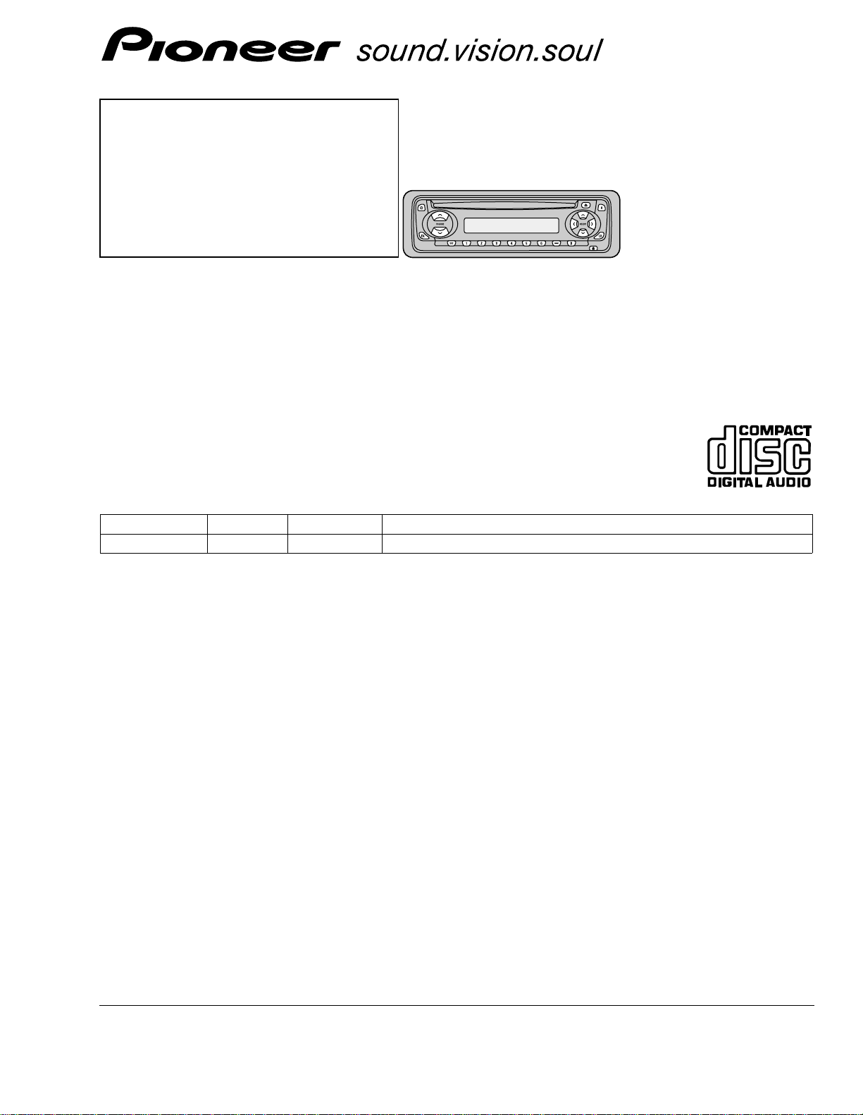
CRT2754
HIGH POWER CD PLAYER WITH FM/AM TUNER
DEH-1400 XM/UC
DEH-1400/XM/UC
CONTENTS
1. SAFETY INFORMATION ............................................2
2. EXPLODED VIEWS AND PARTS LIST.......................2
3. BLOCK DIAGRAM AND SCHEMATIC DIAGRAM.....8
4. PCB CONNECTION DIAGRAM ................................22
5. ELECTRICAL PARTS LIST ........................................30
6. ADJUSTMENT..........................................................34
7. GENERAL INFORMATION .......................................38
7.1 DIAGNOSIS ........................................................38
7.1.1 DISASSEMBLY .........................................38
7.1.2 CONNECTOR FUNCTION DESCRIPTION.......41
7.2 PARTS .................................................................42
7.2.1 IC................................................................42
7.2.2 DISPLAY....................................................50
7.3 OPERATIONAL FLOW CHART...........................51
8. OPERATIONS AND SPECIFICATIONS.....................52
- This service manual should be used together with the following manual(s):
Model No. Order No. Mech. Module Remarks
CX-977 CRT2624 S9 CD Mech. Module:Circuit Description, Mech.Description, Disassembly
DEH-14 XM/UC
Page 2
2
DEH-1400,14
- CD Player Service Precautions
1. For pickup unit(CXX1480) handling, please refer
to"Disassembly"(see page 38).
During replacement, handling precautions shall be
taken to prevent an electrostatic discharge(protection
by a jumper-solder).
2. During disassembly, be sure to turn the power off
since an internal IC might be destroyed when a connector is plugged or unplugged.
3. Please checking the grating after changing the pickup
unit(see page 35).
4. In this product, because the memory capacity of the
microcomputer is insufficient, the test mode is not
installed. However grating of the pickup unit can be
confirmed.
CAUTION
This service manual is intended for qualified service technicians; it is not meant for the casual do-it-yourselfer.
Qualified technicians have the necessary test equipment and tools, and have been trained to properly and safely repair
complex products such as those covered by this manual.
Improperly performed repairs can adversely affect the safety and reliability of the product and may void the warranty.
If you are not qualified to perform the repair of this product properly and safely, you should not risk trying to do so
and refer the repair to a qualified service technician.
W
ARNING
This product contains lead in solder and certain electrical parts contain chemicals which are known to the state of
California to cause cancer, birth defects or other reproductive harm.
Health & Safety Code Section 25249.6 - Proposition 65
1. SAFETY INFORMATION
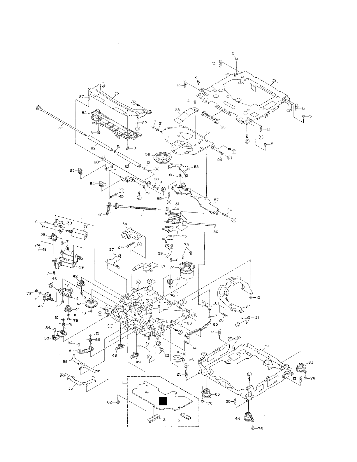
2. EXPLODED VIEWS AND PARTS LIST
2.1 PACKING
14
1
10
12
13
15
17
5
9
2
8
7
6
4
3
16
11
Page 3
3
DEH-1400,14
1 Cord Assy CDE6468
2 Spring CBH1650
3 Screw CBA1002
* 4 Polyethylene Sheet CNM4338
5 Screw CRZ50P090FMC
6 Screw TRZ50P080FMC
* 7 Polyethylene Bag CEG-158
8 Handle CNC5395
9 Bush CNV3930
10 Polyethylene Bag CEG1173
11-1 Owner’s Manual CRD3487
11-2 Installation Manual CRD3492
* 11-3 Card ARY1048
12 Carton
See Contrast table(2)
13 Contain Box See Contrast table(2)
14 Protector CHP2421
15 Protector CHP2422
16 Screw(M3x4) CBA1488
17 Accessory Assy CEA2781
Mark No. Description Part No. Mark No. Description Part No.
(1) PACKING SECTION PARTS LIST
NOTE:
- Parts marked by “*” are generally unavailable because they are not in our Master Spare Parts List.
- Screws adjacent to ∇ mark on the product are used for disassembly.
Part No.
Mark No. Symbol and Description DEH-1400/XM/UC DEH-14/XM/UC
12 Carton CHG4489 CHG4493
13 Contain Box CHL4489 CHL4493
(2) CONTRAST TABLE
DEH-1400/XM/UC and DEH-14/XM/UC are constructed the same except for the following:
- Owner's Manual, Installation Manual
Model Part No. Language
DEH-1400/XM/UC CRD3487 English, French, Spanish
DEH-14/XM/UC CRD3492
Page 4
4
DEH-1400,14
A
B
2.2 EXTERIOR
Page 5

DEH-1400,14
5
1 Screw BMZ30P100FMC
2 Screw BSZ26P060FMC
3 Screw BSZ30P060FMC
4 Cord Assy CDE6468
5 •••••
6 Cable CDE6610
7 Fuse(10A) CEK1136
8
CD Mechanism Module(S9ANA) CXK5501
9 Case CNB2686
10 Holder CNC5704
11 Cushion CNM4870
12 Insulator CNM7622
13 Tuner Amp Unit CWM7942
14 Screw ASZ26P060FMC
15 Screw BPZ26P120FMC
16 Screw BSZ26P160FMC
17 FM/AM Tuner Unit CWE1563
18 Holder CNC8815
19 Pin Jack(CN351) CKB1035
20 Terminal(CN404) CKF1059
21 Plug(CN901) CKM1330
22 Connector(CN751) CKS3581
23 Connector(CN501) CKS3835
24 Antenna Jack(CN402) CKX1056
25 Holder CNC8615
26 Holder CNC9619
27 Insulator CNM6949
28 Heat Sink CNR1583
29 Holder Unit CXB6681
30 Chassis Unit CXB7816
31 Detach Grille Assy
See Contrast table(2)
32 Screw BPZ20P100FZK
33 Button(DETACH) CAC5789
34 Button(EQ) CAC7186
35 Button(SELECT) CAC7181
36 Button(VOL+,-) CAC7182
37 Button(SRC) CAC7187
38 Button(EJECT) CAC7183
39 Button(CLOCK) CAC7298
40 Button(A,LD) CAC7184
41 Button(1-6) CAC7180
42 Spring CBH2210
43 Cover CNS6720
44 Keyboard Unit
See Contrast table(2)
45 LCD See Contrast table(2)
46 Connector(CN1800) CKS3580
47 Holder CNC9617
48 Sheet CNM7057
49 Lighting Conductor CNV6476
50 Connector CNV6868
51 Lighting Conductor CNV6869
52 Rubber CNV6905
53 Grille Unit
See Contrast table(2)
54 Button CAC4836
55 Spring CBH1835
56 Spring CBH2208
57 Spring CBH2367
58 Bracket CNC6791
59 Holder CNC8042
60 Cover CNM6276
61 Panel CNS6722
62 Arm CNV4692
63 Arm CNV4728
64 Arm CNV5576
65 Screw IMS20P030FZK
66 Screw ISS26P055FUC
67 IC(IC361) TDA7386
68 Transistor(Q501,910) 2SD2396
69 •••••
70 Panel CNS6344
(1) EXTERIOR SECTION PARTS LIST
Mark No. Description Part No. Mark No. Description Part No.
Part No.
Mark No. Symbol and Description DEH-1400/XM/UC DEH-14/XM/UC
31 Detach Grille Assy CXB8748 CXB8749
44 Keyboard Unit CWM7955 CWM7956
45 LCD CAW1723 CAW1716
53 Grille Unit CXB8745 CXB8746
(2) CONTRAST TABLE
DEH-1400/XM/UC and DEH-14/XM/UC are constructed the same except for the following:
Page 6
DEH-1400,14
2.3 CD MECHANISM MODULE
6
C
Page 7

7
DEH-1400,14
Mark No. Description Part No. Mark No. Description Part No.
1 Control Unit CWX2481
2 Connector(CN701) CKS1959
3 Connector(CN101) CKS3486
4 Screw BMZ20P025FMC
5 Screw BSZ20P040FMC
6 Screw(M2x4) CBA1362
7 Screw(M2x3) CBA1527
8 Screw CBA1545
9 Washer CBF1037
10 Washer CBF1038
11 Washer CBF1039
12 Washer CBF1060
13 Spring CBH2378
14 Spring CBH2379
15 Spring CBH2514
16 Spring CBH2533
17 Spring CBH2382
18 Spring CBH2383
19 Spring CBH2384
20 Spring CBH2527
21 Spring CBH2386
22 Spring CBH2537
23 Spring CBH2390
24 Spring CBH2391
25 Spring CBH2523
26 Spring CBH2426
27 Spring CBH2444
28 Spring CBL1561
29 Spring CBL1553
30 Shaft CLA3845
31 Roller CLA3910
32 Frame CNC9654
33 Lever CNC9664
34 Lever CNC8949
35 Arm CNC9661
36 Arm CNC9016
37 Arm CNC9017
38 Bracket CNC9123
39 Frame CNC9656
40 Belt CNT1086
41 Gear CNV6886
42 Gear CNV6316
43 Gear CNV6317
44 Gear CNV6318
45 Gear CNV6319
46 Gear CNV6320
47 Arm CNV6322
48 Arm CNV6323
49 Arm CNV6324
50 Arm CNV6888
51 Arm CNV6889
52 Guide CNV6327
53 Arm CNV6924
54 Guide CNV6921
55 Rack CNV6923
56 Clamper CNV6331
57 Arm CNV6332
58 Guide CNV6333
59 Cover CNV6334
60 Arm CNV6335
61 Guide CNV6336
62 Roller CNV6338
63 Damper CNV6339
64 Damper CNV6340
65 Guide CNV6925
66 Chassis Unit CXB7980
* 67 Arm Unit CXB7983
68 Arm Unit CXB7984
69 Arm Unit CXB7985
70 Motor Unit(M2) CXB5903
71 Screw Unit CXB5904
72 Gear Unit CXB8076
73 Bracket Unit CXB7982
74 Motor Unit(M1) CXB6007
75 Arm Unit CXB8504
76 Screw(M2x5) EBA1028
77 Screw JFZ20P020FMC
78 Screw JGZ17P020FZK
79 Washer YE15FUC
80 Washer YE20FUC
81 Pickup Unit(Service)(P9) CXX1480
82 Screw IMS26P030FMC
83 Guide CNV6922
84 Roller CNV6887
85 Spring CBH2509
86 Spring CBH2512
87 Spring CBH2536
88 Collar CNV6906
- CD MECHANISM MODULE SECTION PARTS LIST
Page 8
8
DEH-1400,14
A
1
234
B
C
D
12
34
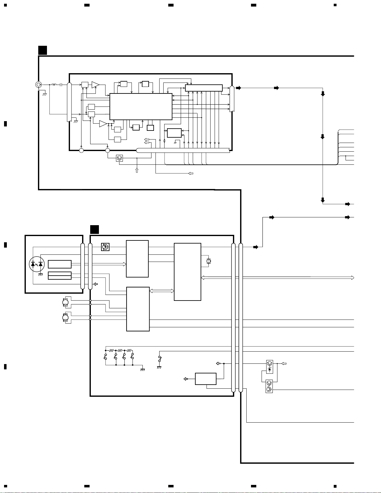
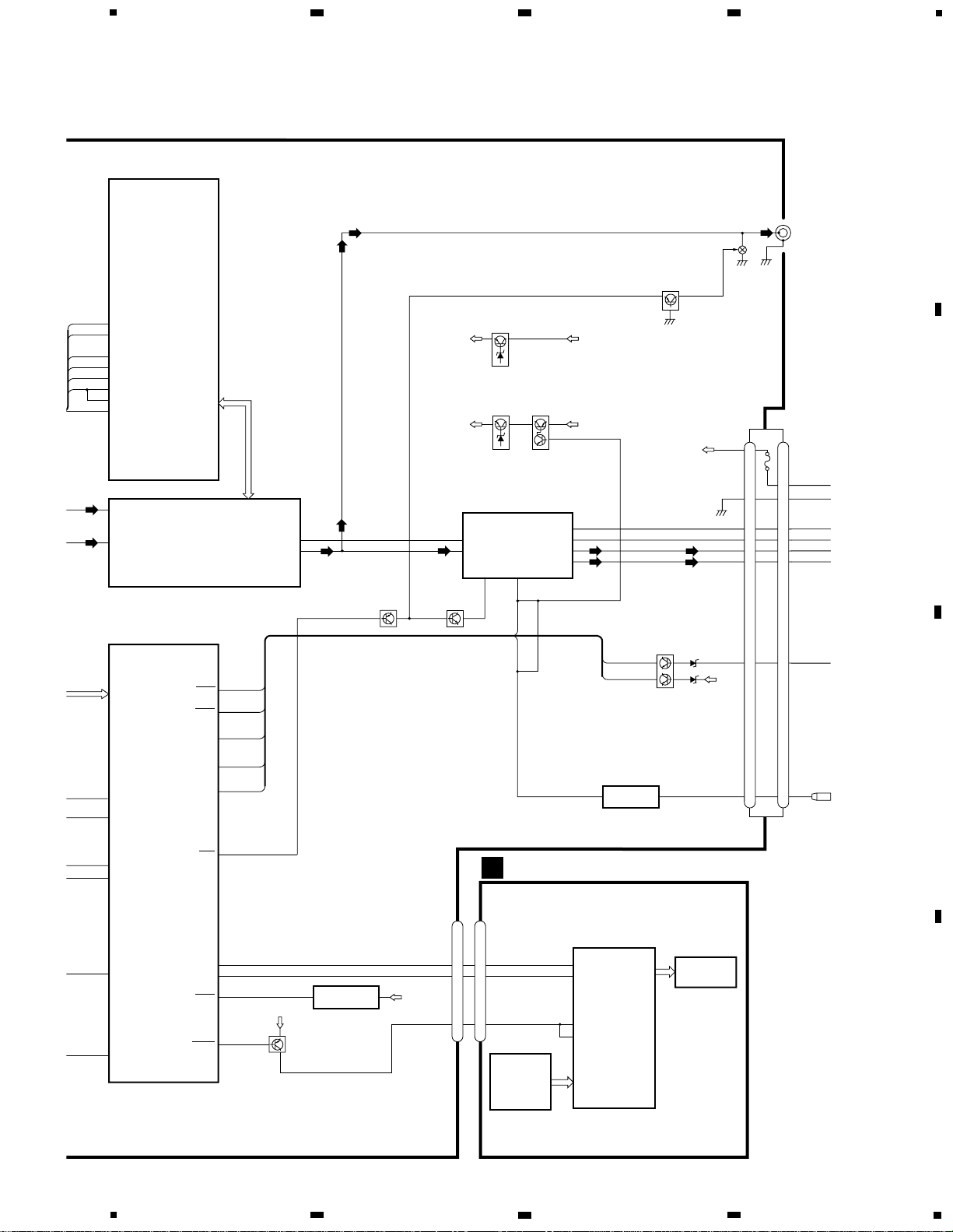
3. BLOCK DIAGRAM AND SCHEMATIC DIAGRAM
3.1 BLOCK DIAGRAM
VDCONT
Q510
Q511
B.U
ANTENNA
CN402
LOCL
Q410
VCC
VDD
PCE2
PCK
PCE1
SL
SD
PDIO
6
76
14
13
48
12
57
2
3
CN501
CDL
34
23
79
32
21
35
LOEJ
CONT
11
PDIO
TUNER AMP UNIT
VD
CD5VON
IC 3
EEPROM
FM/AM TUNER UNIT
28
27
FM/AM 1ST IF 10.7MHz
T51 Q51 CF51
CF52 CF53
IC1
MIXER, IF AMP, DET.
6
21
18
LDET
COMP
222510 14 12 15 16 8 13 2 3 4
CF202
VDD
VCC
DI/DO
CE2CKCE1
SDBWSLFMSD
NL1
NL2
IC 2 FM MPX
AMANT
FMANT
ATT
ATT
AMRF
FMRF
IMG ADJ
RF ADJ
X901
10.25MHz
ANT ADJ
LOCL
23
LOCH
AMDET
MPXREF 41kHz
AM 2ND IF
450kHz
19
CREQ
11
DGND
1
STIND
L ch
5
R ch
924
NC
FMLOCL
20177
NCNCWC
26
RFGND
CN701
Q101
M
LASER
DIODE
MONITOR
DIODE
CLAMP
SENSE
DISC
SENSE
FOCUS ACT.
SPINDLE
MOTOR
M
CARRIAGE
MOTOR
LOAD/
TRACKING ACT.
LD-
MD
FO+
TO+
15
5
1
4
PICKUP UNIT
(SERVICE)(P9)
HOLOGRAM
UNIT
IC 401
BA5996FM
IC 201
TC9495F2
IC 701
BA05SFP
+5V REGULATOR
SERVO
CONTROL,
DSP,
LPF, DAC
CD
DRIVER
17
DSCSNS
2
VD
VD
VDD
11
CONT
10
LOEJ
14
L-OUT
1
CD5VON
CN101
TOP
FOP
16
SOP
15
SOM
17
LCOP
18
LCOM
22
1
2
LOEJ
78
85
L_OUT
79
9
MUTE
12
FOP
TD/FD
AC,BD
F,E
SD/MD
38
RFI
43
FEI
4
14
TOP
S901
HOME
12EJ
SENSE
8EJ
SENSE
HOME
16
LD+
14
VDD
9
LDO
8
MDI
IC 101
TA2153FN
RFRPIN
FEO
TEO
24
16
14
46
TEI
RF-AMP
CONTROL UNIT
17
2
11
10
14
1
16
A
C
PCE1
PCK
PCE2
Page 9
DEH-1400,14
5
6
7
8
A
B
C
D
5
6
7
8
9
KYDT
DPDT
IC 1800
PD6340A
3
4
5
3
4
5
KEY MATRIX
SD
SL
TUNPCE
TUNPCK
TUNPCE2
TUNPDO
LOCL
IN2_L
IN3_L
6
76
14
13
48
12
57
2
3
SYSTEM
CONTROLLER
IC 610 (1/2)
PE5262A
VST
VCK
VDT
B.U
VDD
Q913
B.U
BACKUP
FLFL+
RLRL+
ACC
2
1
10
12
9
11
3
ELECTRONIC VOLUME
IC 301
PML003AM
SYSTEM
CONTROLLER
IC 610(2/2)
PE5262A
ASENS
64
BSENS
63
TELIN
38
SYSPW
42
MUTE
44
KYDT
8
DPDT
9
RESET
60
SWVDD
41
Frontout_L
10
Rearout_L
11
POWER AMP
IC 361
TDA7386
14
12
22 4
5
3
21
23
FL
MUTE STBY
RL
B.U
bsens
asens
Q920
Q361 MUTE
Q921
KEYBOARD UNIT
CN1800CN751
LCD
20
18
Q750
RESET
IC 603
S-80834ANY
VDD
12
SYSPW
6
B.REM
FUSE
10A
CD5VON
34
23
79
32
21
35
VDCONT
HOME
DSCSNS
LOEJ
CONT
TUNPDI
11
PDIO
VST/ VCK/ VDT
VDD
VDD
VLCD
56
10
CN901
Q 351
CN351
REAR L CH
Q359
BACK UP
FL–
FL+
RLRL+
ACC
GND
B
PCE1
PCK
PCE2
ANTIN
52
KYDT
DPDT
SW5V
KEY CONTROLLER
LCD DRIVER
2
1
10
12
9
11
3
6
SYSPW
Q910
Q911
B.U
VCC
Q912
ANTPW
B.REMOTE
IC 901
TPD1018F
61
RESET
IC 603
S-80834ANY
12
VCC REGULATOR
VDD REGULATOR
B.REM
Page 10
10
DEH-1400,14
A
1
234
B
C
D
12
34
3.2 OVERALL CONNECTION DIAGRAM(GUIDE PAGE)
Note: When ordering service parts, be sure to refer to “EXPLODED VIEWS AND PARTS LIST” or “ELECTRICAL PARTS
LIST”.
A-a A-b
A-aA-a
A-b A-b
A-b A-b
A-a A-a
Large size
SCH diagram
Guide page
Detailed page
A
C
CONTROL UNIT
B
CN1800
FM/AM TUNER UNIT
A
183
183
162
162
272
272
104
CSS1023 4.194304MHz
FMLOCL
682
0R0
R791
ANTENNA
JACK
For resistors and capacitors in the circuit diagrams, their resistance values or
capacitance values are expressed in codes:
Ex. *Resistors
Code Practical value
123 12k ohms
103 10k ohms
*Capacitors
Code Practical value
103 0.01µF
101/10 100µF/10V
The > mark found on some component parts indicates
the importance of the safety factor of the part.
Therefore, when replacing, be sure to use parts of
identical designation.
Symbol indicates a resistor.
No differentiation is made between chip resistors and
discrete resistors.
NOTE :
Symbol indicates a capacitor.
No differentiation is made between chip capacitors and
discrete capacitors.
ELECTRONIC
SYST
FM(100%):-19.5dBs
AM(30%):-30dBs
A-a
Page 11
11
DEH-1400,14
5
6
7
8
A
B
C
D
5
6
7
8
A
A
TUNER AMP UNIT
CEK1136
>
10A
RR+
RR-
FR+
FR-
FL+
FL-
RL+
RL-
ACC
GND
B.REM
BACK UP
RR
RL
PRE OUT
VOLUME
EM CONTROLLER
MUTE
POWER AMP
VDD REGULATOR
BACK UP SENSE
ACC SENSE
B.REMOTE
VCC REGULATOR
SYS+B REGULATOR
FM(100%):+3.6dBs
AM(30%):-6.9dBs
CD:+10.2dBs
CD:+9.4dBs
FM(100%):+29.6dBs
AM(30%):+19.1dBs
CD:+36.2dBs
A-b
Page 12
12
DEH-1400,14
A
1
234
B
C
D
12
34
A-a
A-a
A-b
FM/AM TUNER UNIT
183
183
162
162
272
272
CSS1023 4.194304MHz
FMLOCL
682
0R0
R791
ANTENNA
JACK
ELECTRONIC VOLU
SYSTEM CO
FM(100%):-19.5dBs
AM(30%):-30dBs
1
Page 13
13
DEH-1400,14
5
6
7
8
A
B
C
D
5
6
7
8
A-a
A-b
C
CONTROL UNIT
B
CN1800
A
104
For resistors and capacitors in the circuit diagrams, their resistance values or
capacitance values are expressed in codes:
Ex. *Resistors
Code Practical value
123 12k ohms
103 10k ohms
*Capacitors
Code Practical value
103 0.01µF
101/10 100µF/10V
The > mark found on some component parts indicates
the importance of the safety factor of the part.
Therefore, when replacing, be sure to use parts of
identical designation.
Symbol indicates a resistor.
No differentiation is made between chip resistors and
discrete resistors.
NOTE :
Symbol indicates a capacitor.
No differentiation is made between chip capacitors and
discrete capacitors.
6
7
5
2
3
4
A-a
Page 14
14
DEH-1400,14
A
1
234
B
C
D
12
34
A-a
A-b
A-b
A
TUNER AMP UNIT
RR
RL
PRE OUT
MUTE
POWER AMP
FM(100%):+3.6dBs
AM(30%):-6.9dBs
CD:+10.2dBs
CD:+9.4dBs
FM(100%):+29.6dBs
AM(30%):+19.1dBs
CD:+36 2dBs
1
Page 15
15
DEH-1400,14
5
6
7
8
A
B
C
D
5
6
7
8
A-b
A-a
A-b
CEK1136
>
10A
RR+
RR-
FR+
FR-
FL+
FL-
RL+
RL-
ACC
GND
B.REM
BACK UP
VDD REGULATOR
BACK UP SENSE
ACC SENSE
B.REMOTE
VCC REGULATOR
SYS+B REGULATOR
FM(100%):+29.6dBs
AM(30%):+19.1dBs
CD:+36.2dBs
6
7
5
2
3
4
Page 16
16
DEH-1400,14
A
1
234
B
C
D
12
34
3.3 KEYBOARD UNIT
LCD DRIVER
LCD
B
KEYBOARD UNIT
B
Page 17
DEH-1400,14
5
6
7
8
A
B
C
D
5
6
7
8
17
CLOCK
LOC/BSM
DEH-1400/XM/UC
SML-310PT
CEL1651
CAW1723
820
121
D1702-1708
IL1700,1701
LCD
R1711
R1715,1719
DEH-14/XM/UC
SML-310DT
CEL1638
CAW1716
121
181
IL1700,1701:14V 40mA
A
CN751
B
Page 18

18
DEH-1400,14
A
1
234
B
C
D
12
34
3.4 CD MECHANISM MODULE
C
M1 CXB6007
M2 CXB5903
LOADING/CARRIAGE
SPINDLE
RF AMP
S
ACT/MOTOR DRIVER
5V REGULATOR
CN101
C
CONTROL UNIT
PICKUP UNIT(SERVICE)(P9)
Page 19

DEH-1400,14
5
6
7
8
A
B
C
D
5
6
7
8
19
C
16.934MHz
SERVO CONTROL/DSP/DAC/LPF
CN701
SWITCHES:
CONTROL UNIT
S901 : HOME SWITCH.....ON-OFF
S902 : CLAMP SWITCH....ON-OFF
S903 : DSCSNS SWITCH....ON-OFF
S904 : 12EJ SWITCH....ON-OFF
S905 : 8EJ SWITCH....ON-OFF
The underlined indicates the switch position.
A
CN501
Decimal points for resistor
and capacitor fixed values
are expressed as :
2.2
→2R2
0.022→R022
Page 20

20
DEH-1400,14
@ CH1:BCK 2V/div.
During "Play"
1 CH1:DSCSNS 5V/div.
2 CH2:CLCONT 5V/div.
3 CH3:LOEJ 5V/div.
4 CH4:VD 10V/div.
When loading (8 cm CD)
500ms/div.
5 CH1:FD 500mV/div.
6 CH2:FOK 5V/div.
7 CH3:MD 5V/div.
When setting up "Source On"
500ms/div.
8 CH1:FE 500mV/div.
9 CH2:FOON 5V/div.
When setting up "Source On"
500ms/div.
5 CH1:FD 500mV/div.
6 CH2:FOK 5V/div.
7 CH3:MD 5V/div.
Magnified drawing for "time"
100ms/div.
1 CH1:DSCSNS 5V/div.
2 CH2:CLCONT 5V/div.
3 CH3:LOEJ 5V/div.
4 CH4:VD 10V/div.
When loading (12 cm CD)
Ref. :
GND
Mode :
Normal
Ref. :
GND
Mode :
Normal
Ref. :
VREF
Mode :
Normal
Ref. :
VREF
Mode :
Normal
Ref. :
VREF
Mode :
Normal
Ref. :
VREF
Mode :
Normal
Ref. :
VREF
Mode :
Normal
Ref. :
VREF
Mode :
Normal
Ref. :
VREF
Mode :
Normal
Ref. :
VREF
Mode :
Test
Ref. :
VREF
Mode :
Normal
Ref. :
VREF
Mode :
Normal
500ms/div.
0 CH1:TE 500mV/div.
8 CH2:FE 500mV/div.
When setting up "Source On"
200ms/div.
1µs/div.
# CH1:LRCK 2V/div.
$ CH2:DOUT 2V/div.
During "Play"
10µs/div.
7 CH1:MD 500mV/div.
During "Play"
10µs/div.
% CH1:RFO 500mV/div.
During "Play"
0.5µs/div.
% CH1:RFO 500mV/div.
0 CH2:TE 500mV/div.
During "Tracking Open"
2ms/div.
8 CH1:FE 500mV/div.
5 CH2:FD 500mV/div.
0 CH3:TE 500mV/div.
! CH4:TD 500mV/div.
During "Play"
1ms/div.
- Waveforms
Note:1. The encircled numbers denote measuring pointes in the circuit diagram.
2. Reference voltage
VREF:2.1V
Page 21

21
DEH-1400,14
% CH1:RFO 1V/div.
0 CH2:TE 500mV/div.
& CH3:DFCT 5V/div.
During inside/outside search
200ms/div.
% CH1:RFO 1V/div.
0 CH2:TE 500mV/div.
! CH3:TD 1V/div.
1 Track Jump
500µs/div.
% CH1:RFO 1V/div.
0 CH2:TE 1V/div.
! CH3:TD 1V/div.
100 Track Jump
5ms/div.
% CH1:RFO 1V/div.
0 CH2:TE 1V/div.
! CH3:TD 1V/div.
32 Track Jump
5ms/div.
5 CH1:FD 1V/div.
^ CH2:FOP 2V/div.
With no disk inserted
During "Focus Close"
200ms/div.
1 CH1:DSCSNS 5V/div.
2 CH2:CLCONT 5V/div.
3 CH3:LOEJ 5V/div.
When "Eject" (8cm CD)
200ms/div.
) CH1:LOUT 2V/div.
⁄ CH2:ROUT 2V/div.
"Play" in 1kHz, 0dB
200µs/div.
* CH1:TEY 500mV/div.
( CH2:SD 2V/div.
During inside/outside search
200ms/div.
1 CH1:DSCSNS 5V/div.
2 CH2:CLCONT 5V/div.
3 CH3:LOEJ 5V/div.
When "Eject" (12 cm CD)
200ms/div.
% CH1:RFO 2V/div.
& CH2:DFCT 5V/div.
5 CH3:FD 1V/div.
! CH4:TD 2V/div.
When reproducing black dots (800µm)
500µs/div.
Ref. :
VREF
Mode :
Test
Ref. :
VREF
Mode :
Test
Ref. :
VREF
Mode :
Normal
Ref. :
VREF
Mode :
Normal
Ref. :
VREF
Mode :
Test
Ref. :
VREF
Mode :
Test
Ref. :
VREF
Mode :
Normal
Ref. :
GND
Mode :
Normal
Ref. :
GND
Mode :
Normal
Ref. :
GND
Mode :
Normal
Page 22

22
DEH-1400,14
A
1
234
B
C
D
12
34
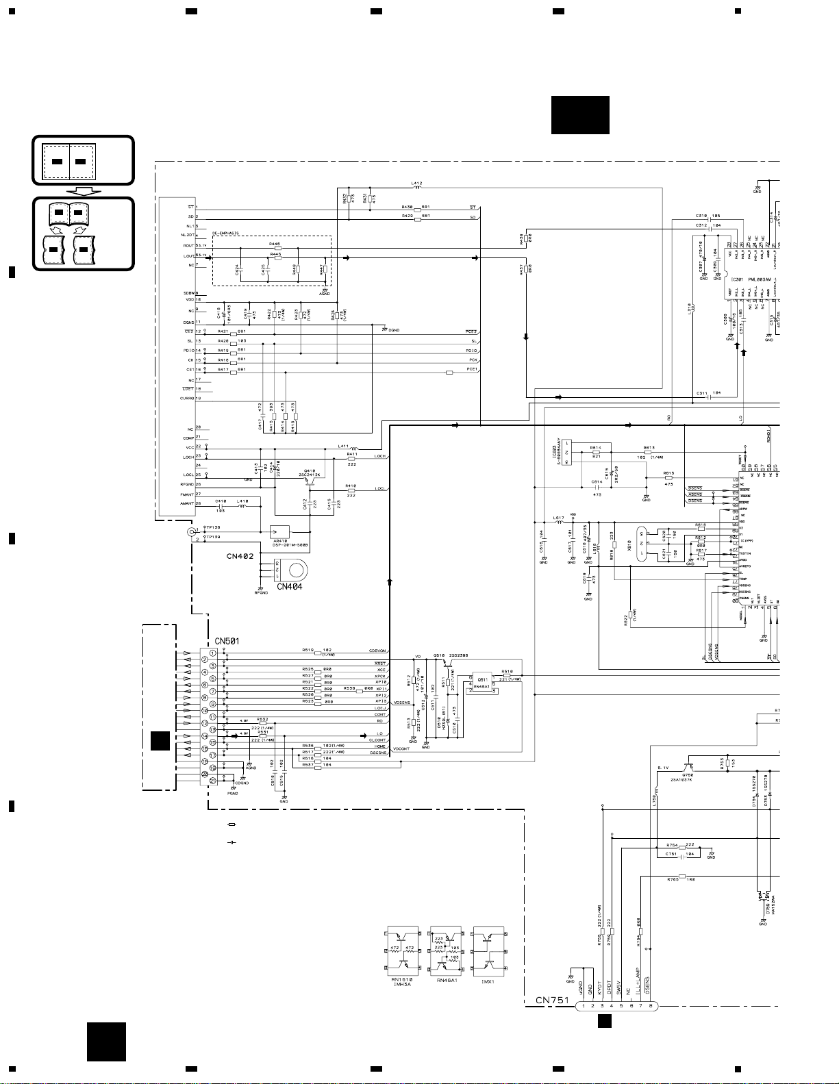
NOTE FOR PCB DIAGRAMS
1. The parts mounted on
this PCB include all necessary parts for several
destination.
For further information
for respective destinations, be sure to check
A
Capacitor
Connector
P.C.Board
Chip Part
SIDE A
SIDE B
2
345678910111213
141
15
16
A
A
TUNER AMP UNIT
C
CN701
CORD ASSY
4. PCB CONNECTION DIAGRAM
4.1 TUNER AMP UNIT
Page 23

DEH-1400,14
5
6
7
8
A
B
C
D
5
6
7
8
23
A
1
3
45
6782
ANTENNA
JACK
B
CN1800
FM/AM TUNER UNIT
FRONT
SIDE A
Page 24

24
DEH-1400,14
A
1
234
B
C
D
12
34
A
1
3
6
4
1
3
6
4
4
6
3
1
A
TUNER AMP UNIT
Page 25

DEH-1400,14
5
6
7
8
A
B
C
D
5
6
7
8
25
463
1
4
6
3
1
4
6
3
1
SIDE B
A
Page 26

26
DEH-1400,14
A
1
234
B
C
D
12
34
B
KEYBOARD UNIT
B
KEYBOARD UNIT
A
CN751
←
←
←
←
EJECT
AUDIO
LOUD
BANDLOC/BSM654321SOURCE
VOL+
VOL-
CLOCK
EQ
LCD
4.2 KEYBOARD UNIT
SIDE A
B
SIDE B
Page 27

27
DEH-1400,14
Page 28

28
DEH-1400,14
A
1
234
B
C
D
12
34
E
F
VREF
HOME
12EJ
DSCSNS
4.3 CD MECHANISM MODULE
CONTROL UNIT
SIDE A
C
C
M2 LOADING/CARRIAGE MOTOR
M1 SPINDLE MOTOR
PICKUP UNIT(SERVICE)(P9)
CN501
A
Page 29

DEH-1400,14
1
2
3
4
A
B
C
D
1
2
3
4
29
CLAMP
8EJ
SIDE B
CONTROL UNIT
C
C
Page 30

30
DEH-1400,14
5. ELECTRICAL PARTS LIST
NOTES:
- Parts whose parts numbers are omitted are subject to being not supplied.
- The part numbers shown below indicate chip components.
Chip Resistor
RS1/_S___J,RS1/__S___J
Chip Capacitor (except for CQS.....)
CKS....., CCS....., CSZS.....
=====Circuit Symbol and No.===Part Name Part No.
--- ------ ------------------------------------------ -------------------------
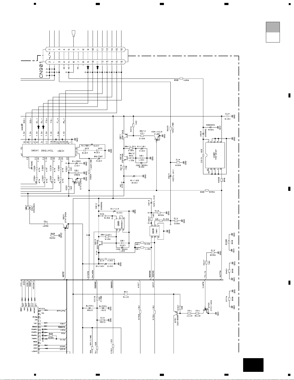
Unit Number : CWM7942
Unit Name : Tuner Amp Unit
MISCELLANEOUS
IC 301 IC PML003AM
IC 361 IC TDA7386
IC 603 IC S-80834ANY
IC 610 IC PE5262A
IC 901 IC TPD1018F
Q 351 Transistor IMH3A
Q 359 Transistor DTA124EK
Q 361 Transistor DTC124EK
Q 410 Transistor 2SC2412K
Q 510 Transistor 2SD2396
Q 511 Transistor RN46A1
Q 750 Transistor 2SA1037K
Q 751 Transistor 2SA1036K
Q 753 Transistor DTC114EK
Q 909 Transistor RN46A1
Q 910 Transistor 2SD2396
Q 911 Transistor 2SB1243
Q 912 Transistor DTC114EK
Q 913 Transistor 2SD1859
Q 920 Transistor IMX1
Q 921 Transistor DTA124EK
D 510 Diode HZS9L(B1)
D 750 Diode 1SS270
D 751 Diode 1SS270
D 753 Diode 1SS270
D 754 Diode 1SS270
D 759 Diode MA152WA
D 910 Diode HZS9L(B3)
D 911 Diode HZS6L(B2)
D 912 Diode S5688G
D 913 Diode HZS7L(C2)
D 914 Diode HZS7L(A1)
D 919 Diode S5688G
D 920 Diode S5688G
D 921 Diode DAN202U
D 923 Diode S5688G
D 924 Diode S5688G
L 310 Inductor LAU1R0K
L 361 Choke Coil 600µH CTH1221
L 410 Ferri-Inductor LAU4R7K
L 411 Ferri-Inductor LAU2R2K
L 412 Ferri-Inductor LAU2R2K
L 617 Ferri-Inductor LAU101K
L 618 Ferri-Inductor LAU2R2K
L 750 Ferri-Inductor LAU2R2K
X 610 Crystal Resonator 4.194304MHz CSS1023
AR 410 Surge Protector DSP-201M-S00B
FM/AM Tuner Unit CWE1563
RESISTORS
R 310 RS1/16S101J
R 311 RS1/16S101J
R 314 RS1/16S101J
R 315 RS1/16S101J
R 351 RD1/4PU821J
R 352 RS1/16S821J
R 353 RS1/16S223J
R 354 RS1/16S223J
R 355 RS1/16S0R0J
R 361 RS1/16S103J
R 362 RS1/16S103J
R 363 RS1/16S331J
R 364 RD1/4PU153J
R 410 RS1/16S222J
R 411 RS1/16S222J
R 413 RS1/16S473J
R 414 RS1/16S473J
R 415 RS1/16S393J
R 417 RS1/16S681J
R 418 RS1/16S681J
R 419 RS1/16S681J
R 420 RS1/16S103J
R 421 RS1/16S681J
R 422 RD1/4PU473J
R 423 RD1/4PU472J
R 424 RD1/4PU473J
R 429 RS1/16S681J
R 430 RS1/16S681J
R 431 RS1/16S473J
R 432 RS1/16S473J
R 437 RS1/16S0R0J
R 438 RS1/16S0R0J
R 445 RS1/16S272J
R 446 RS1/16S272J
R 447 RS1/16S162J
R 448 RS1/16S162J
R 490 RS1/16S0R0J
R 510 RD1/4PU221J
R 511 RD1/4PU221J
R 512 RD1/4PU472J
R 513 RD1/4PU222J
R 516 RS1/16S104J
R 517 RD1/4PU222J
R 519 RD1/4PU102J
R 520 RS1/16S0R0J
R 521 RS1/16S0R0J
R 522 RS1/16S0R0J
R 523 RS1/16S0R0J
R 525 RS1/16S0R0J
R 527 RS1/16S0R0J
=====Circuit Symbol and No.===Part Name Part No.
--- ------ ------------------------------------------ -------------------------
A
Page 31

31
DEH-1400,14
R 531 RD1/4PU222J
R 532 RD1/4PU222J
R 536 RD1/4PU102J
R 537 RS1/16S104J
R 538 RS1/16S0R0J
R 612 RS1/16S0R0J
R 613 RD1/4PU102J
R 614 RS1/16S821J
R 615 RS1/16S473J
R 616 RS1/16S682J
R 617 RS1/16S473J
R 618 RS1/16S223J
R 622 RD1/4PU104J
R 625 RS1/16S0R0J
R 712 RD1/4PU104J
R 750 RD1/4PU104J
R 751 RS1/16S103J
R 752 RS1/16S153J
R 753 RS1/16S153J
R 754 RS1/16S222J
R 755 RD1/4PU222J
R 758 RS1/16S102J
R 759 RS1/16S222J
R 764 RS1/16S0R0J
R 765 RS1/16S1R0J
R 767 RS1/16S103J
R 769 RS1/16S102J
R 774 RS1/16S0R0J
R 775 RS1/16S1R0J
R 777 RS1/16S152J
R 778 RS1/16S152J
R 779 RD1/4PU103J
R 791 RS1/16S0R0J
R 910 RS1/16S1R0J
R 911 RD1/4PU220J
R 912 RD1/4PU132J
R 913 RD1/4PU122J
R 914 RS1/16S103J
R 915 RS1/16S222J
R 916 RD1/4PU153J
R 917 RS1/16S104J
R 918 RS1/16S104J
R 919 RS1/16S104J
R 920 RS1/16S473J
R 921 RS1/16S103J
R 922 RS1/16S473J
R 923 RD1/4PU102J
R 924 RS1/16S472J
R 927 RS1/16S102J
R 928 RS1/16S473J
R 929 RS1/16S0R0J
R 930 RS1/16S0R0J
R 931 RS1/16S0R0J
R 937 RS1/16S152J
R 939 RS1/16S0R0J
CAPACITORS
C 307 CEJQ470M10
C 308 CEJQ100M16
C 309 CKSRYB104K25
C 310 CKSRYB105K6R3
C 311 CKSRYB104K25
C 312 CKSRYB104K25
C 313 CKSRYB105K6R3
C 314 CEJQ4R7M35
C 315 CEJQ4R7M35
C 316 CKSRYB153K25
C 321 CKSRYB153K25
C 324 CCSRCH100D50
C 326 CCSRCH100D50
C 327 CCSRCH100D50
C 329 CCSRCH100D50
C 351 CEJQ2R2M50
C 352 CEJQ2R2M50
C 361 3300µF/16V CCH1368
C 362 CKSRYB104K25
C 363 CKSQYB474K16
C 364 CKSQYB474K16
C 365 CKSQYB474K16
C 366 CKSQYB474K16
C 367 CKSQYB474K16
C 368 CKSQYB474K16
C 369 CKSQYB474K16
C 370 CKSQYB474K16
C 371 CEJQ330M10
C 372 CEJQ2R2M50
C 373 CKSQYB225K10
C 374 CKSQYB225K10
C 375 CEJQ100M16
C 410 CKSQYB103K25
C 412 CKSRYB223K50
C 413 CKSRYB102K50
C 414 CEJQ220M10
C 415 CKSRYB223K50
C 417 CKSRYB472K50
C 418 CEJQ101M6R3
C 419 CKSRYB473K50
C 424 CKSRYB183K25
C 425 CKSRYB183K25
C 510 CKSRYB473K50
C 511 CKSRYB102K50
C 512 CEJQ101M10
C 515 CKSRYB102K50
C 516 CKSRYB102K50
C 614 CKSRYB473K50
C 615 CEJQ2R2M50
C 616 CKSRYB104K25
C 617 CCSRCH101J50
C 618 CEJQ4R7M35
C 619 CKSRYB473K50
C 620 CCSRCH150J50
C 621 CCSRCH150J50
C 751 CKSRYB104K25
C 910 330µF/16V CCH1326
C 911 CKSRYB103K50
C 912 CEJQ101M16
C 913 CEJQ101M10
C 914 CKSRYB473K50
C 915 CKSRYB103K50
C 916 470µF/16V CCH1331
C 918 CKSQYB473K50
C 919 CKSRYB103K50
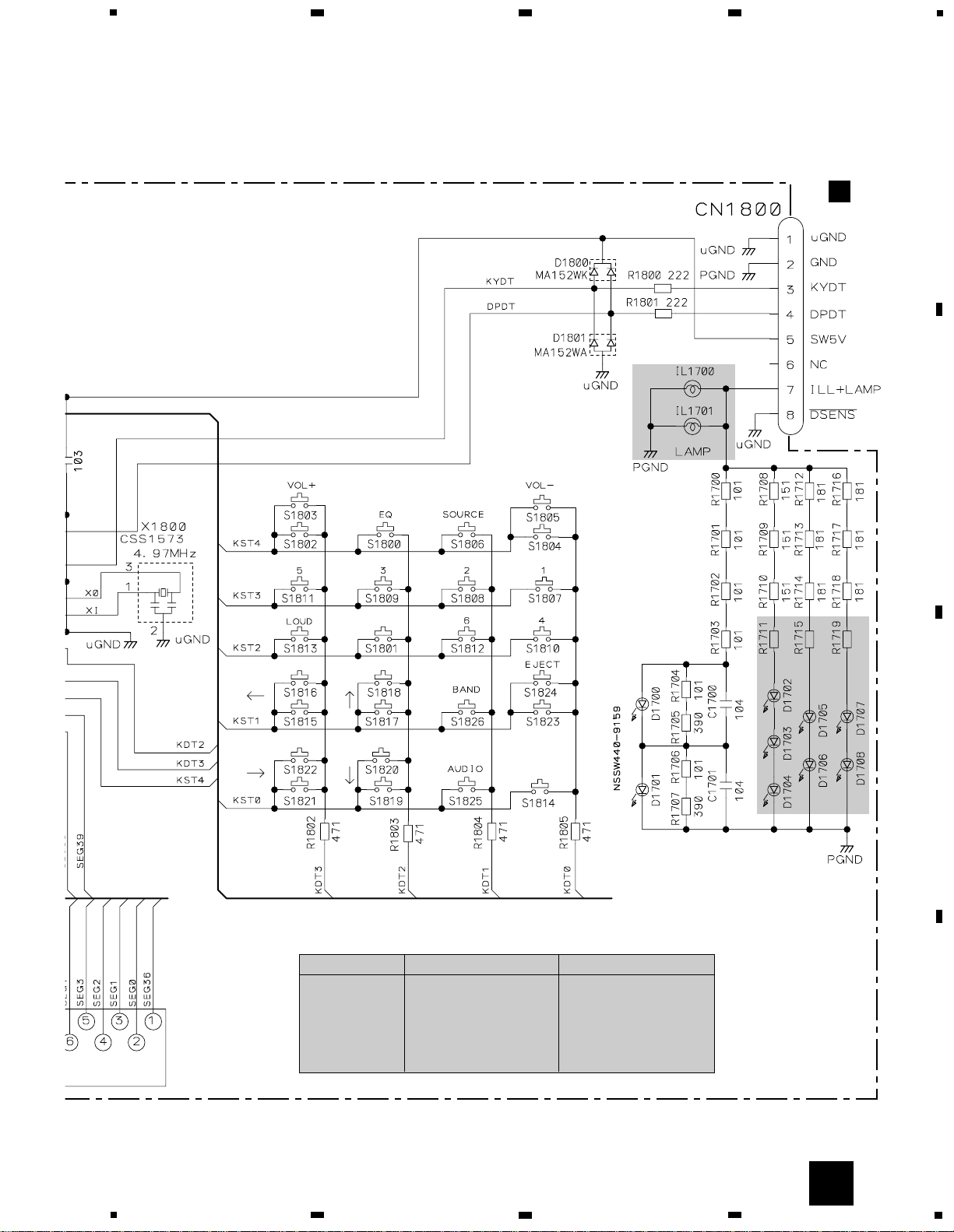
Unit Number : CWM7955(DEH-1400/XM/UC)
Unit Name : Keyboard Unit
MISCELLANEOUS
IC 1800 IC PD6340A
D 1700 LED NSSW440-9159
D 1701 LED NSSW440-9159
D 1702 LED SML-310PT
D 1703 LED SML-310PT
=====Circuit Symbol and No.===Part Name Part No.
--- ------ ------------------------------------------ -------------------------
=====Circuit Symbol and No.===Part Name Part No.
--- ------ ------------------------------------------ -------------------------
B
Page 32

32
DEH-1400,14
D 1704 LED SML-310PT
D 1705 LED SML-310PT
D 1706 LED SML-310PT
D 1707 LED SML-310PT
D 1708 LED SML-310PT
D 1800 Diode MA152WK
D 1801 Diode MA152WA
X 1800 Ceramic Resonator 4.97MHz CSS1573
IL 1700 Lamp 14V 40mA CEL1651
IL 1701 Lamp 14V 40mA CEL1651
LCD CAW1723
RESISTORS
R 1700 RS1/16S101J
R 1701 RS1/16S101J
R 1702 RS1/16S101J
R 1703 RS1/16S101J
R 1708 RS1/16S151J
R 1709 RS1/16S151J
R 1710 RS1/16S151J
R 1711 RS1/16S820J
R 1712 RS1/16S181J
R 1713 RS1/16S181J
R 1714 RS1/16S181J
R 1715 RS1/16S121J
R 1716 RS1/16S181J
R 1717 RS1/16S181J
R 1718 RS1/16S181J
R 1719 RS1/16S121J
R 1800 RS1/16S222J
R 1801 RS1/16S222J
R 1802 RS1/16S471J
R 1803 RS1/16S471J
R 1804 RS1/16S471J
R 1805 RS1/16S471J
CAPACITORS
C 1700 CKSQYF104Z50
C 1701 CKSQYF104Z50
C 1800 CKSRYB103K50
Unit Number : CWM7956(DEH-14/XM/UC)
Unit Name : Keyboard Unit
MISCELLANEOUS
IC 1800 IC PD6340A
D 1700 LED NSSW440-9159
D 1701 LED NSSW440-9159
D 1702 LED SML-310DT
D 1703 LED SML-310DT
D 1704 LED SML-310DT
D 1705 LED SML-310DT
D 1706 LED SML-310DT
D 1707 LED SML-310DT
D 1708 LED SML-310DT
D 1800 Diode MA152WK
D 1801 Diode MA152WA
X 1800 Ceramic Resonator 4.97MHz CSS1573
IL 1700 Lamp 14V 40mA CEL1638
IL 1701 Lamp 14V 40mA CEL1638
LCD CAW1716
RESISTORS
R 1700 RS1/16S101J
R 1701 RS1/16S101J
R 1702 RS1/16S101J
R 1703 RS1/16S101J
R 1708 RS1/16S151J
R 1709 RS1/16S151J
R 1710 RS1/16S151J
R 1711 RS1/16S121J
R 1712 RS1/16S181J
R 1713 RS1/16S181J
R 1714 RS1/16S181J
R 1715 RS1/16S181J
R 1716 RS1/16S181J
R 1717 RS1/16S181J
R 1718 RS1/16S181J
R 1719 RS1/16S181J
R 1800 RS1/16S222J
R 1801 RS1/16S222J
R 1802 RS1/16S471J
R 1803 RS1/16S471J
R 1804 RS1/16S471J
R 1805 RS1/16S471J
CAPACITORS
C 1700 CKSQYF104Z50
C 1701 CKSQYF104Z50
C 1800 CKSRYB103K50
Unit Number : CWX2481
Unit Name : Control Unit
MISCELLANEOUS
IC 101 IC TA2153FN
IC 201 IC TC9495F2
IC 401 IC BA5996FM
IC 701 IC BA05SFP
Q 101 Transistor 2SD1664
Q 102 Transistor UMD2N
L 201 Inductor CTF1546
L 202 Inductor CTF1546
X 301 Ceramic Resonator 16.934MHz CSS1525
S 901 Spring Switch(HOME) CSN1051
S 902 Spring Switch(CLAMP) CSN1052
S 903 Spring Switch(DSCSNS) CSN1051
S 904 Spring Switch(12EJ) CSN1052
S 905 Spring Switch(8EJ) CSN1051
RESISTORS
R 101 RS1/16S222J
R 102 RS1/8S120J
R 103 RS1/8S100J
R 201 RS1/16S513J
R 202 RS1/16S513J
R 203 RS1/16S823J
R 204 RS1/16S823J
R 206 RS1/16S823J
R 208 RS1/16S124J
R 209 RS1/16S183J
R 210 RS1/16S153J
R 211 RS1/16S103J
R 212 RS1/16S103J
R 213 RS1/16S124J
R 215 RS1/16S0R0J
R 216 RS1/16S471J
R 301 RS1/16S333J
R 302 RS1/16S332J
R 303 RS1/16S332J
R 304 RS1/16S514J
R 306 RS1/16S102J
R 307 RS1/16S102J
R 312 RS1/16S103J
R 313 RS1/16S473J
R 315 RS1/16S334J
=====Circuit Symbol and No.===Part Name Part No.
--- ------ ------------------------------------------ -------------------------
=====Circuit Symbol and No.===Part Name Part No.
--- ------ ------------------------------------------ -------------------------
B
C
Page 33

33
DEH-1400,14
R 321 RS1/16S331J
R 322 RS1/16S0R0J
R 323 RS1/16S332J
R 401 RS1/16S684J
R 402 RS1/16S103J
R 403 RS1/16S103J
R 404 RS1/16S183J
R 405 RS1/16S123J
R 407 RS1/16S622J
R 408 RS1/16S622J
R 409 RS1/16S113J
R 410 RS1/16S752J
R 701 RS1/16S102J
R 702 RS1/16S221J
R 703 RS1/16S221J
R 704 RS1/16S221J
R 705 RS1/16S221J
R 706 RS1/16S221J
R 707 RS1/16S221J
R 708 RS1/16S102J
R 709 RS1/16S102J
R 710 RS1/16S102J
R 901 RS1/16S104J
R 902 RS1/16S473J
R 903 RS1/16S273J
CAPACITORS
C 101 CEV470M6R3
C 102 CKSRYB102K50
C 103 CKSRYB104K16
C 104 CKSRYB224K16
C 105 CEV470M6R3
C 106 CKSRYB104K16
C 107 CKSRYB105K6R3
C 201 CKSRYB104K16
C 202 CCSRCH560J50
C 204 CKSRYB224K16
C 205 CKSRYB224K16
C 206 CKSRYB273K25
C 207 CKSRYB273K25
C 208 CKSRYB104K16
C 209 CKSRYB104K16
C 210 CCSRCK2R0C50
C 211 CCSRCH220J50
C 301 CKSRYB153K25
C 302 CKSRYB104K16
C 303 CKSRYB103K50
C 304 CKSRYB103K50
C 305 CKSRYB104K16
C 306 CKSRYB104K16
C 307 CKSRYB333K16
C 308 CKSRYB104K16
C 309 CKSRYB473K16
C 310 CKSRYB473K16
C 311 CKSRYB104K16
C 312 CKSRYB104K16
C 315 CEV220M6R3
C 317 CKSRYB104K16
C 318 CKSRYB104K16
C 319 CKSRYB104K16
C 320 CCSRCH470J50
C 325 CKSRYB471K50
C 328 CKSRYB472K50
C 329 CKSRYB104K16
C 330 CKSRYB104K16
C 331 CKSRYB104K16
C 401 CKSRYB221K50
C 402 CKSRYB221K50
C 403 CKSRYB153K25
C 404 CKSRYB103K50
C 405 CEV101M10
C 702 CKSRYB104K16
C 703 CKSRYB104K16
C 801 10µF/10V CCH1349
C 802 CEV101M10
C 803 CKSRYB224K16
Miscellaneous Parts List
Pickup Unit(Service)(P9) CXX1480
M 1 Motor Unit(SPINDLE) CXB6007
M 2 Motor Unit(LOADING/CARRIAGE) CXB5903
=====Circuit Symbol and No.===Part Name Part No.
--- ------ ------------------------------------------ -------------------------
=====Circuit Symbol and No.===Part Name Part No.
--- ------ ------------------------------------------ -------------------------
Page 34

34
DEH-1400,14
6. ADJUSTMENT
6.1 CD ADJUSTMENT
1) Precautions
• This unit uses a single power supply (+5V) for the regulator. The signal reference potential, therefore, is
connected to VREF(approx. 2.1V) instead of GND.
If VREF and GND are connected to each other by mistake during adjustments, not only will it be impossible to measure the potential correctly, but the servo
will malfunction and a severe shock will be applied to
the pick-up. To avoid this, take special note of the following.
Do not connect the negative probe of the measuring
equipment to VREF and GND together. It is especially
important not to connect the channel 1 negative
probe of the oscilloscope to VREF with the channel 2
negative probe connected to GND.
Since the frame of the measuring instrument is usually at the same potential as the negative probe, change
the frame of the measuring instrument to floating status.
If by accident VREF comes in contact with GND,
immediately switch the regulator or power OFF.
• Always make sure the regulator is OFF when connecting and disconnecting the various filters and wiring
required for measurements.
• Before proceeding to further adjustments and measurements after switching regulator ON, let the player
run for about one minute to allow the circuits to stabilize.
• Since the protective systems in the unit's software are
rendered inoperative in test mode, be very careful to
avoid mechanical and /or electrical shocks to the system when making adjustment.
• The RFI and RFO signals are easy to oscillate because
of a wide band. When observing them, insert a resistor of about 1 kΩ to the series.
• This equipment will not guarantee the load ejection
operation when the mechanical unit is turned upside
down. In particular, if the ejection operation is incorrectly performed and recovery is disabled, the recovery is enabled by resetting a product or turning ACC
off to on.
2) Test Mode
This mode is used for adjusting the CD mechanism
module of the device.
• Test mode starting procedure
Reset while pressing the 4 and 6 keys together.
• Test mode cancellation
Switch ACC, back-up OFF.
• After pressing the EJECT key, do not press any other
key until the disk is completely ejected.
• If the ] or [ key is pressed while focus search is in
progress, immediately turn the power off (otherwise
the actuator may be damaged due to adhesion of the
lenses).
Page 35

35
DEH-1400,14
• Note :
The grating angle of the PU unit cannot be adjusted after the PU unit is changed. The PU unit in the CD mecha-
nism module is adjusted on the production line to match the CD mechanism module and is thus the best adjusted
PU unit for the CD mechanism module. Changing the PU unit is thus best considered as a last resort. However, if
the PU unit must be changed, the grating should be checked using the procedure below.
• Purpose :
To check that the grating is within an acceptable range when the PU unit is changed.
• Symptoms of Mal-adjustment :
If the grating is off by a large amount symptoms such as being unable to close tracking, being unable to perform
track search operations, or taking a long time for track searching.
• Method :
• Measuring Equipment • Oscilloscope, Two L.P.F.
• Measuring Points • E, F, VREF
• Disc • ABEX TCD-784
• Mode • TEST MODE
• Checking Procedure
1. In test mode, load the disc and switch the 5V regulator on.
2. The display will change, returning to "81" on the fourth press.
3. As shown in the diagram above, monitor the LPF outputs using the oscilloscope and check that the phase difference is within 75° . Refer to the photographs supplied to determine the phase angle.
4. If the phase difference is determined to be greater than 75° try changing the PU unit to see if there is any
improvement. If, after trying this a number of times, the grating angle does not become less than 75° then the
mechanism should be judged to be at fault.
• Note
Because of eccentricity in the disc and a slight misalignment of the clamping center the grating waveform may be
seen to "wobble" ( the phase difference changes as the disc rotates). The angle specified above indicates the average angle.
• Hint
Reloading the disc changes the clamp position and may decrease the "wobble".
100kΩ
390pF
100kΩ
390pF
E
VREF
F
VREF
Xch Ych
L.P.F.
L.P.F.
VREF
E
F
6.2 CHECKING THE GRATING AFTER CHANGING THE PICKUP UNIT
CONTROL UNIT
Oscilloscope
Page 36

36
DEH-1400,14
Grating waveform
Ech → Xch 20mV/div, AC
Fch → Ych 20mV/div, AC
45°
0°
75°
60°
30°
90°
Page 37

37
DEH-1400,14
6.3 ERROR MODE
- Error Messages
If a CD is not operative or stopped during operation due to an error, the error mode is turned on and cause(s) of the
error is indicated with a corresponding number. This arrangement is intended at reducing nonsense calls from the
users and also for facilitating trouble analysis and repair work in servicing.
(1) Basic Indication Method
1) When SERRORM is selected for the CSMOD (CD mode area for the system), error codes are written to DMIN (minutes display area) and DSEC (seconds display area). The same data is written to DMIN and DSEC. DTNO remains
in blank as before.
2) Head unit display examples
Depending on display capability of LCD used, display will vary as shown below. xx contains the error number.
8-digit display 6-digit display 4-digit display
ERROR–xx ERR–xx E–xx
(2) Error Code List
Code Class Displayed error code Description of the code and potential cause(s)
10 Electricity Carriage Home NG CRG can't be moved to inner diameter.
SERVO LSI Com- CRG can't be moved from inner diameter.
munication Error → Failure on home switch or CRG move mechanism.
Communication error between microcomputer and SERVO LSI.
11 Electricity Focus Servo NG Focusing not available.
→ Stains on rear side of disc or excessive vibrations on REWRITABLE.
12 Electricity Spindle Lock NG Spindle not locked. Sub-code is strange (not readable).
Subcode NG → Failure on spindle, stains or damages on disc, or excessive vibrations.
A disc not containing CD-R data is found.
Turned over disc are found, though rarely.
CD signal error.
17 Electricity Setup NG AGC protection doesn't work. Focus can be easily lost.
→ Damages or stains on disc, or excessive vibrations on REWRITABLE.
30 Electricity Search Time Out Failed to reach target address.
→ CRG tracking error or damages on disc.
44 Electricity ALL Skip Skip setting for all track.
(CD-R/RW)
50
Mechanism CD On Mech Error Mechanical error during CD ON.
→ Defective loading motor, mechanical lock and mechanical sensor.
A0 System Power Supply NG Power (VD) is ground faulted.
→ Failure on SW transistor or power supply (failure on connector).
Remarks: Mechanical errors are not displayed (because a CD is turned off in these errors).
Unreadable TOC does not constitute an error. An intended operation continues in this case.
Upper digits of an error code are subdivided as shown below:
1x: Setup relevant errors, 3x: Search relevant errors, Ax: Other errors.
Page 38

38
DEH-1400,14
7. GENERAL INFORMATION
7.1 DIAGNOSIS
7.1.1 DISASSEMBLY
- Removing the Tuner Amp Unit (Fig.2)
Remove the two screws.
Straight the tabs at three locations indicated.
Remove the three screws.
Remove the screw and then remove the Tuner
Amp Unit.
- Removing the Case (not shown)
1. Remove the Case.
- Panel Assy (Fig.1)
Take the two stoppers off the Chassis and then
remove the Panel Assy.
- Removing the CD Mechanism Module (Fig.1)
Remove the four screws and then remove the
CD Mechanism Module.
Fig.1
Fig.2
Tuner Amp Unit
CD Mechanism Module
Panel Assy
Page 39

39
DEH-1400,14
- How to hold the Mechanical Unit
1.Hold the top and bottom frame.
2.Do not squeeze top frame's front portion too tight,
because it is fragile.
- How to remove the Top and Bottom Frame
1.When the disk is in "clamp" state, unlock Spring A (6
pieces) and Spring B (2 pieces), and unscrew screws
(4 pieces).
2.Unlock each 1 of pawl at the both side of the frame,
then remove the top frame.
3.Remove the Carriage Mechanical part in such way
that; you remove the mechanical part from 3 pieces
of Damper while slowly pulling up the part.
4.Now, the top frame has been removed, and under
this state, fix the genuine Connector again, and eject
the disk.
(Caution)
When you reassemble the Carriage Mechanical part,
apply a bit of alcohol to Dampers.
- How to remove the Guide Arm Assy
1.Unlock the spring (1 piece) at the right side of the
assembly.
2.Unscrew screws (2 pieces), then remove the Screw
Gear Bracket.
3.Shift the Guide Arm Assy to the left and slowly rotate
it to the upper direction.
4.When the Guide Arm Assy rotates approximately 45
degree, shift the Assy to the right side direction and
remove it.
Top Frame
Bottom Frame
Damper
Spring
Screw Gear Bracket
Guide Arm
Assy
Carriage
Mechanical
Part
Do not squeeze.
Page 40

40
DEH-1400,14
- How to remove the Control Unit
1.Give jumper-solder treatment to the Flexible Wire of
the Pickup unit, then remove the wire from the
Connector.
2.Remove all 4 points of solder-treatment on the Lead
Wire. Also, unscrew the screw(1 piece).
3.Then, Remove the Control unit.
(Caution)
Be careful not to damage SW when you reassemble
the Control Unit into the device.
- How to remove the Loading Arm Assy
1.Unlock the spring (1 piece) and remove the E ring (1
piece) of the Fulcrum Shaft.
2.Shift the arm to the left side direction and unlock pins
(2 pieces).
- How to remove the Pickup Unit
1.Unscrew 2 pieces of screws, then remove the Pulley
Cover.
2.Remove the Feed Screw unit from the pawl of the
Feed Screw Guide (The pawl is located inside the
guide).
3.Remove the belt from the Pulley, then remove the
Pickup unit.
(Caution)
Make sure not to stain the belt with grease when you
fix the belt.
Control Unit
Jumper-Solder
Solder
Loading Arm Assy
Pickup Unit
Pulley Cover
Feed Screw Guide
Belt
Grease Application
Grease Application
Grease Application
Page 41

41
DEH-1400,14
7.1.2 CONNECTOR FUNCTION DESCRIPTION
57913
468210121416
111315
PRE OUTANTENNA
1. GND
2. BACK UP
3. ACC
4. NC
5. NC
6. B.REM
7. NC
8. NC
9. RL-
10. FL-
11. RL+
12. FL+
13. RR-
14. FR-
15. RR+
16. FR+
Page 42

42
DEH-1400,14
7.2 PARTS
7.2.1 IC
- Pin Functions(PE5262A)
Pin No. Pin Name I/O Format Function and Operation
1 MODEL1 I Model select input
2,3 NC Not used
4 AVSS I A/D GND
5 ST I FM stereo input
6 SD I SD input
7 AVREF1 A/D converter reference voltage
8 KYDT I Key data input
9 DPDT O C Display data output
10 SDBW I SDBW input
11 TUNPDI I PLL IC data input
12 TUNPDO O C PLL IC data output
13 TUNPCK O C PLL IC clock output
14 TUNPCE O C PLL IC chip enable output
15 currq O Tuner voltage FIX output
16 LOCL O C Local L output
17 NC Not used
18 fm/AM O C FM/AM power select output
19 NC Not used
20 FLPILM O C Inside of flap illumination output
21 VDCONT O C VD control output
22 NC Not used
23 CONT O C Servo driver power supply control output
24 XCE O C CD LSI chip enable output
25 xrst O C CD LSI reset output
26 XPCK O C CD LSI clock output
27-30 XPI0-3 I/O C CD LSI data input/output
31 CLCONT O C Driver input select output
32 HOME I C Home position detector input
33 VSS GND
34 LOEJ O C CD load motor LOAD/EJECT direction exchange output
35 CD5VON O C CD +5V power supply control output
36,37 ROT1-0 I Rotary encoder data input
38 TELIN I Telephone mute input
39 NC Not used
40 ILMPW O C Illumination power supply control output
41 swvdd O C Keyboard unit power supply control output
42 SYSPW O C System power supply control output
43 VST O C Strobe pulse output for electronic volume
44 mute O C System mute output
45 PEE O C Beep tone output
46 LOCH O C Local H output
47 NC Not used
48 TUNPCE2 O C EEPROM chip enable output
49 PCL O C Clock adjustment output
50 VCK O C Clock output for electronic volume
51 VDT O C Data output for electronic volume
52 ANTPW O Antenna output
53 EJECTS I Eject key input pin
54 DALMON O C Stand-by output
55–59 NC Not used
60 reset I Reset input
61,62 NC Not used
63 bsens I Back up power sense input
64 asens I ACC power sense input
65 dsens I Grille detach sense
66 ADPW O C A/D converter power supply output
67 NC Not used
Page 43

43
DEH-1400,14
Pin No. Pin Name I/O Format Function and Operation
68 VDD Power supply
69 X2 Crystal oscillator connection pin
70 X1 I Crystal oscillator connection pin
71 IC(VPP) Connect to GND
72 NC Not used
73 TESTIN I Test program mode input
74 AVDD Positive power supply terminal for analog circuit
75 AVREF0 A/D converter reference voltage
76 SL I SD level input from tuner
77 TEMP I CD temperature sense input
78 VDSENS I VD power supply voltage sense input
79 DISCSNS I CD DISC sense input
80 CSENS I Flap open/close sense input
80
1
20
21 40
41
60
61
*PE5262A
Output Format Meaning
C C MOS output
N N channel open drain output
IC's marked by * are MOS type.
Be careful in handling them because they are very
liable to be damaged by electrostatic induction.
Page 44

44
DEH-1400,14
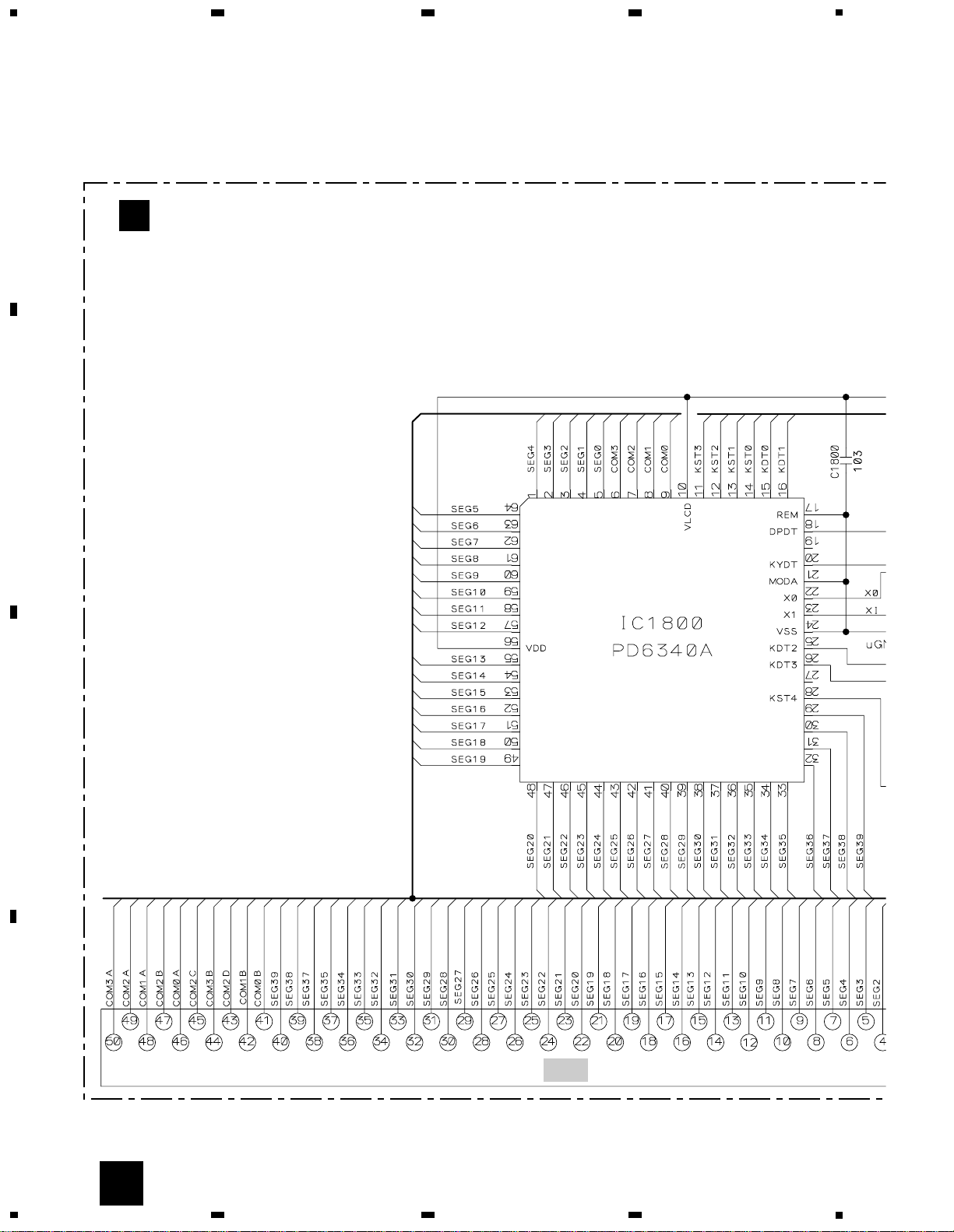
- Pin Functions (PD6340A)
Pin No. Pin Name I/O Function and Operation
1-5 SEG4-0 O LCD segment output
6-9 COM3-0 O LCD common output
10 VLCD LCD drive power supply
11-14 KST3-0 O Key strobe output
15,16 KDT0,1 I Key data input (analogue input)
17 REM I Remote control reception
18 DPDT I Display data input
19 NC Not used
20 KYDT O Key data output
21 MODA GND
22 X0 Crystal oscillator connection pin
23 X1 Crystal oscillator connection pin
24 VSS GND
25,26 KDT2,3 I Key data input
27 NC Not used
28 KST4 O Key strobe output
29-32 NC Not used
33-55 SEG35-13 O LCD segment output
56 VDD Power supply
57-64 SEG12-5 O LCD segment output
*PD6340A
32
17
33
16
48
49
64
1
Page 45

45
DEH-1400,14
- Pin Functions(TA2153FN)
Pin No. Pin Name I/O Function and Operation
1 VCC Power supply voltage terminal
2 RFGC I RF amplitude adjustment control signal terminal
3 GMAD I AGC amplifier frequency characteristic adjustment terminal
4 FNI I Main beam amplifier input terminal
5 FPI I Main beam amplifier input terminal
6 TPI I Sub beam amplifier input terminal
7 TNI I Sub beam amplifier input terminal
8 MDI O Monitor photodiode amplifier input terminal
9 LDO I Laser diode amplifier output terminal
10 SEL I APC circuit ON/OFF signal, LDO terminal control input terminal and bottom
and peak detection frequency switching terminals
11 TEB I Tracking error balance adjustment signal input terminal
12 2VRO O Reference voltage (2VRO) output terminal
13 TEN I Tracking error signal generation amplifier reverse phase input terminal
14 TEO O Tracking error signal generation amplifier output terminal
15 SBAD O Sub beam addition signal output terminal
16 FEO O Focus error signal generation amplifier output terminal
17 FEN I Focus error signal generation amplifier reverse phase input terminal
18 SEB I RFRP generation circuit mode switching terminal
19 VRO O Reference voltage (VREF) output terminal
20 RFRP O Signal generation amplifier output terminal for track count
21 BTC I Bottom detection time constant adjustment terminal for RFCT signal
generation
22 RFCT O RFRP signal center level output terminal
23 PKC I Peak detection time constant adjustment signal for RFCT signal generation
24 RFRPIN I Signal generation amplifier input terminal for track count
25 RFGO O RF signal amplitude adjustment amplifier output terminal
26 GVSW I AGC, FE or TE amplifier gain switching terminal
27 AGCIN I RF signal amplitude adjustment amplifier input terminal
28 RFO O RF signal generation amplifier output terminal
29 GND I GND terminal
30 RFN2 I RF signal generation amplifier input terminal
1
15
16
30
TA2153FN
Page 46

46
DEH-1400,14
- Pin Functions(TC9495F2)
Pin No. Pin Name I/O Function and Operation
1 TESTO Test mode terminal
2 hso O Replay speed flag output terminal
3 uhso O Replay speed flag output terminal
4 EMPH O Emphasis flag output terminal for sub code Q data
5 LRCK O Channel clock (44.1 kHz) output terminal
6 VSS Digital ground terminal
7 BCK O Bit clock output terminal
8 AOUT O Digital audio data output terminal
9 DOUT O Digital out output terminal
10 MBOV O Buffer memory over signal output terminal
11 IPF O Correction flag output terminal
12 SBOK O CRCC decision result output for sub code Q data
13 CLCK I/O Clock input/output terminal for sub code P-W data read
14 VDD Digital + power supply terminal (5 V)
15 VSS Digital ground terminal
16 DATA O Sub code P-W data output terminal
17 SFSY O Replay-system frame sync signal output terminal
18 SBSY O Sub code block sync output terminal
19 SPCK O Clock for processor status signal read
20 SPDA O Processor status signal output terminal
21 COFS O Correction-system frame clock (7.35 kHz) output terminal
22 MONIT O LSI internal signal output terminal
23 VDD Digital + power supply terminal (5 V)
24 TESIO0 I Test input/output terminal
25 P2VREF PLL-system only 2VREF terminal
26 HSSW O The VREF voltage is reached for double or quad speed.
27 ZDET O One-bit DAC zero detection flag output terminal
28 PDO O Phase error signal issue between the EFM and PLCK signals
29 TMAXS O TMAX detection result output terminal
30 TAMX O TMAX detection result output terminal
31 LPFN I Reverse input terminal of amplifier for lowpass filter
32 LPFO O Output terminal of amplifier for lowpass filter
33 PVREF PLL-system only VREF terminal
34 VCOREF I VCO center frequency reference level terminal
35 VCOF O Filter terminal for VCO
36 AVSS Analog-system ground terminal
37 SLCO O Output terminal of DAC for data slice level generation
38 RFI I RF signal input terminal
39 AVDD Analog-system power supply terminal (5 V)
40 RFCT I RFRP signal center level input terminal
41 RFZI I Input terminal for RFRP signal zero cross
42 RFRP I RF ripple signal input terminal
43 FEI I Focus error signal input terminal
44 SBAD I Sub beam addition signal input terminal
45 TSIN I Test input terminal
46 TEI I Tracking error input terminal
47 TEZI I Input terminal for tracking error or zero cross
48 FOO O Focus equalizer output terminal
49 TRO O Tracking equalizer output terminal
50 VREF Analog reference power supply terminal
51 RFGC O RF amplitude adjustment control signal output terminal
52 TEBC O Tracking balance control signal output terminal
53 FMO O Feed equalizer output terminal
54 FVO O Speed error signal or feed search EQ output
55 DMO O Disc equalizer output terminal
56 2VREF Analog reference power supply terminal
57 SEL O APC circuit ON/OFF signal output terminal
Page 47

47
DEH-1400,14
Pin No. Pin Name I/O Function and Operation
58-61 FLGA-D O External flag output terminal for internal signal monitor
62 VDD Digital + power supply terminal (5 V)
63 VSS Digital ground terminal
64 IO0 O RF amplifier gain switching terminal
65 IO1 O Not used
66 IO2 I HOME detection switch input terminal
67 IO3 O FocusDrv and signal output terminal
68 dmout I Field equalizer PWM output terminal for IO0 and IO1
Disc equalizer PWM output terminal for IO2 and IO3
69 ckse I Usually open
70 dact I DAC test mode terminal
71 TESIN I Test input terminal
72 TESIO1 I Test input/output terminal
73 VSS Digital ground terminal
74 PXI I DPS-system clock oscillator circuit input terminal
75 PXO O DPS-system clock oscillator circuit output terminal
76 VDD Digital + power supply terminal (5 V)
77 XVSS Ground terminal for system clock oscillator circuit
78 XI I System clock oscillator circuit input terminal
79 XO O System clock oscillator circuit output terminal
80 XVDD For system clock oscillator circuit + power supply terminal
81 DVSR R channel D/A converting unit power supply terminal
82 RO O R channel data forward rotation output terminal
83 DVDD D/A converting unit power supply terminal (5 V)
84 DVR Reference voltage terminal
85 LO O L channel forward rotation output terminal
86 DVSL L channel D/A converting unit power supply terminal
87-89 TEST1-3 I Test mode terminal
90-93 BUS0-3 I/O Data input/output terminal for microcomputer interface
94 VDD Digital + power supply terminal (5 V)
95 VSS Digital ground terminal
96 BUCK I Clock terminal for microcomputer interface
97 cee I Chip enable signal for microcomputer interface
98 TEST4 I Test mode terminal
99 tsmod I Test mode terminal
100 rst I Reset signal input terminal
30
31
50
51
80
81
100
1
*TC9495F2
Page 48

48
DEH-1400,14
- Pin Functions(BA5996FM)
Pin No. Pin Name Function and Operation
1 VR Input pin for reference voltage
2 OPIN2(+) Input pin for non-inverting input for CH2 preamplifier
3 OPIN2(-) Input pin for inverting input for CH2 preamplifier
4 OPOUT2 Output pin for CH2 preamplifier
5 OPIN1(+) Input pin for non-inverting input for CH1 preamplifier
6 OPIN1(-) Input pin for inverting input from CH1 preamplifier
7 OPOUT1 Output pin for CH1 preamplifier
8 GND Ground pin
9 MUTE Mute control pin
10 POWVCC1 Power supply pin for CH1, CH2, and CH3 at "Power" stage
11 VO1(-) Driver CH1 - Negative output
12 VO1(+) Driver CH2 - Positive output
13 VO2(-) Driver CH2 - Negative output
14 VO2(+) Driver CH2 - Positive output
15 VO3(+) Driver CH2 - Positive output
16 VO3(-) Driver CH2 - Negative output
17 VO4(+) Driver CH4 - Positive output
18 VO4(-) Driver CH4 - Negative output
19 POWVCC2 Power supply pin for CH4 at "Power" stage
20 GND Ground pin
21 CNT Control pin
22 LDIN Loading input
23 OPOUTSL Output pin for preamplifier for thread
24 OPINSL Input pin for preamplifier for thread
25 OPOUT3 CH3 preamplifier output pin
26 OPIN3(-) Input pin for inverting input for CH3 preamplifier
27 OPIN3(+) Input pin for non-inverting input for CH3 preamplifier
28 PREVCC PreVcc
BA5996FM
114
15 28
Page 49

49
DEH-1400,14
No. Symbol I/O Explain
1 STIND O stereo "Low" when the FM stereo signals are received.
indicator To be pulled up to the "VDD" at 47kΩ.
2 FMSD O FM station "High" when signals are received. To be pulled up to the "VDD" at 47kΩ
detector Meanwhile, 10kΩ should be used when taking diver FIX trigger from here
and "High: 0.9VDD or more" and "Low: 250mV or less".
(Should satisfy the diver IC specifications)
3 NL1 O noise level-1 "High" when noise is received. Output for the RDS. GND at 47kΩ //1,800pF.
4 NL2 O noise level-2 "High" when noise is received. Output for the RDS. GND at 36kΩ //330pF.
5 Rch O R channel FM stereo "R-ch" signal output or AM audio output.
output Add the specified de-emphasis constant.
6 Lch O L channel FM stereo "L-ch" signal output or AM audio output.
output Add the specified de-emphasis constant.
7 WC write control EEPROM write control. Writing permissible at "Low". Normally open.
8 SDBW O SD bandwidth SD bandwidth signal output. For detection of detuning data for the RDS.
9 NC Not used
10 VDD power Power supply pin for the digital section.
supply DC 5V +/- 0.25V. Be careful about overlapping noise in the logic section.
11 DGND digital ground Grounding for the digital section.
12 CE2 I chip enable-2 EEPROM chip enable. Active a "Low"
To be pulled up to the "VDD" at 47kΩ
13 SL I/O signal level Received FM/AM signal level (strength) output.
Connect the specified load resistor and capacitor (10k Ω + 39k Ω //4,700pF)
14 DI/DO I/O data input/ Data input/Data output
data output To be pulled up to the "VDD" at 47kΩ
15 CK I clock Clock input To be pulled up to the "VDD" at 47kΩ
16 CE1 I chip enable-1 AF·RF chip enable. Active at "High" To be grounded at 47kΩ
17 NC Not used
18 LDET O lock detector Active at "Low". To be pulled up to the "VDD" at 47kΩ
19 CREQ I current request Active at "Low". To be grounded at 47kΩ
20 NC Not used
21 COMP O composite signal FM composite signal output. r out < 100Ω
22 VCC power supply Analog section power supply pin.DC 8.4V +/- 0.3V
23 LOCH I local high FM local high pin. When seeking local high, apply 5V together with "LOCL".
24 FMLOCL I FM local low FM local low pin. When seeking local low, apply 5V to the base of the NPN
transistor with which the specified resistor is being connected to the emitter.
Keep it open in case of ordinary marketed models.
25 LOCL I local low FM/AM local low pin. When seeking local low, apply 5V to the base of the
NPN transistor.
Since this pin is exclusive for AM when the FMLOCL is in use,
do not drive it under FM.
26 RFGND RF ground Grounding for the antenna section.
27 FMANT I FM antenna input FM antenna input. 75Ω. Surge absorber (DSP-201M-S00B) is necessary.
28 AMANT I AM antenna input AM antenna input. High impedance.
Connect to the antenna through an L (LAU type) of 4.7µH.To cope with the
power transmission line hums, insert a series circuit consisting of an L
(a coil of about 100mH) + R (a resistor of 470 Ω to 2.2kΩ) between the GND.
IC 3
EEPROM
28
27
FM/AM 1ST IF 10.7MHz
T51 Q51 CF51
CF52 CF53
IC1
MIXER, IF AMP, DET.
6
21
18
LDET
COMP
222510 14 12 15 16 8 13 2 3 4
CF202
VDD
VCC
DI/DO
CE2CKCE1
SDBWSLFMSD
NL1
NL2
IC 2 FM MPX
AMANT
FMANT
ATT
ATT
AMRF
FMRF
IMG ADJ
RF ADJ
X901
10.25MHz
ANT ADJ
LOCL
23
LOCH
AMDET
MPXREF 41kHz
AM 2ND IF
450kHz
19
CREQ
11
DGND
1
STIND
L ch
5
R ch
924
NC
FMLOCL
20177
NCNCWC
26
RFGND
- FM/AM Tuner Unit
Page 50

DEH-1400,14
SEG37
SEG35
SEG34
SEG33
SEG32
SEG31
SEG30
SEG29
SEG28
SEG27
SEG26
SEG25
SEG24
SEG23
SEG22
SEG21
SEG20
SEG18
SEG17
SEG16
SEG15
SEG14
SEG13
SEG12
SEG11
SEG10
SEG9
SEG8
SEG7
SEG6
SEG5
SEG4
SEG3
SEG2
NC
NC
SEG19
SEG36
COM2B
COM0A
COM2C
COM3B
COM2D
COM1B
COM0B
SEG39
SEG38
COM3A
COM2A
COM1A
37
36
35
34
33
32
31
30
29
28
27
26
25
24
23
22
20
19
18
17
16
15
14
13
12
11
10
9
8
7
6
5
4
3
2
21
1
47
46
45
44
43
42
41
39
38
50
49
48
40
COM2B
COM0A
COM2C
COM3B
COM2D
COM1B
COM0B
COM3A
COM2A
COM1A
COMMON
SEGMENT
7.2.2 DISPLAY
- CAW1723(DEH-1400/XM/UC), CAW1716(DEH-14/XM/UC)
50
Page 51

DEH-1400,14
51
7.3 OPERATIONAL FLOW CHART
VDD=5V
Pin 68
Power ON
BSENS=L
ASENS=L
DSENS=L
bsens
Pin 63
asens
Pin 64
dsens
Pin 65
ADPW←H
Pin 66
swvdd←L
Pin 41
Source keys
operative
Completes power-on operation.(After that, proceed to each source operation.)
SYSPW←H
Pin 42
Starts communication with Grille microcomputer.
Source ON
300ms
300ms
In case of the above signal, the communication
with Grille microcomputer may fail.
If the time interval is not 300msec, the oscillator
may be defective.
Page 52

52
DEH-1400,14
8. OPERATIONS AND SPECIFICATIONS
8.1 OPERATIONS
What’s what
1 VOLUME button
Press to increase or decrease the volume.
2 CD EJECT button
Press to eject a CD from your built-in CD player.
3 AUDIO button
Press to select various sound quality controls.
4 CLOCK button
Press to switch clock display on or off.
5 EQ button
Press to select various equalizer curves.
6 5/∞/2/3 buttons
Press to do manual seek tuning, fast forward, reverse
and track search controls. Also used for controlling
functions.
7 LOUDNESS button
Press to switch loudness function on or off.
8 SOURCE button
This unit is switched on by selecting a source. Press to
cycle through all of the available sources.
9 1–6 (PRESET TUNING) buttons
Press for preset tuning.
0 LOCAL/BSM button
! BAND button
Press to select among three FM and one AM band and
cancel the control mode of functions.
@ DETACH button
Press to remove the front panel from the head unit.
1
3
4
5
6
7
8
9
0
!
@
2
Page 53

53
DEH-1400,14
Power ON/OFF
Tuner
Turning the unit on
Press SOURCE to turn the unit on.
When you select a source the unit is turned
on.
Selecting a source
You can select a source you want to listen
to. To switch to the built-in CD player, load a
disc in this unit
Press
SOURCE to select a source.
Press
SOURCE repeatedly to switch between
the following sources:
Built-in CD player—
Tuner
Notes
• When no disc is set in this product, built-in
CD player source will not change.
• When this unit’s blue/white lead is con-
nected to the car’s auto-antenna relay
control terminal, the car’s antenna
extends when this unit’s source is
switched on. To retract the antenna,
switch the source off.
Turning the unit off
Press SOURCE and hold for at least one sec-
ond to turn the unit off.
Listening to the radio
1 BAND indicator
Shows which band the radio is tuned to,
AM or FM.
2 FREQUENCY indicator
Shows to which frequency the tuner is
tuned.
3 STEREO () indicator
Shows that the frequency selected is
being broadcast in stereo.
4 PRESET NUMBER indicator
Shows what preset has been selected.
Built-in CD player
1 Press
SOURCE to select the tuner.
2 Use VOLUME to adjust the sound level.
When you press
VOLUME up/+, the volume is
raised and when pressed down/–, the vol-
ume is lowered.
3 Press BAND to select a band.
Press BAND until the desired band is dis-
played, FM1, FM2
, FM3 for FM or AM.
4 To perform manual tuning, press 2 or 3
with quick presses.
The frequencies move up or down step by
step.
5 To perform seek tuning, press and hold 2
or 3 for about one second and release.
The tuner will scan the frequencies until a
broadcast strong enough for good reception
is found.
• You can cancel seek tuning by pressing
either
2 or 3 with a quick press.
• If you press and hold 2 or 3 you can skip
broadcasting stations. Seek tuning starts as
soon as you release the buttons.
Note
• When the frequency selected is being
broadcast in stereo the STEREO () indica-
tor will light.
Playing a CD
1 TRACK NUMBER indicator
Shows the track currently playing.
2 PLAY TIME indicator
Shows the elapsed playing time of the
current track.
1 Insert a CD into the CD loading slot.
Playback will automatically start.
CD loading slot
• You can eject a CD by pressing CD EJECT.
2 After a CD has been inserted, press
SOURCE to select the built-in CD player.
3 Use VOLUME to adjust the sound level.
When you press VOLUME up/+, the volume is
raised and when pressed down/–, the vol-
ume is lowered.
21
4
3
2
1
Page 54

54
DEH-1400,14
Audio Adjustments
Introduction of audio adjust-
ments
1 AUDIO display
Shows the audio adjustments status.
2 LOUD indicator
Appears in the display when loudness is
turned on.
Press AUDIO to display the audio function
names.
Press AUDIO repeatedly to switch between
the following audio functions:
FADER (balance adjustment)—EQ
(equalizer)—LOUD (loudness)—FIE (front
image enhancer)—SLA (source level adjust-
ment)
• When selecting the FM tuner as the
source, you cannot switch to SLA.
• To return to the display of each source,
press BAND.
Note
• If you do not operate the audio function
within about 30 seconds, the display is
automatically returned to the source dis-
play.
Using balance adjustment
You can select a fader/balance setting that
provides an ideal listening environment in
all occupied seats.
1 Press AUDIO to select FADER.
Press AUDIO until FADER appears in the dis-
play.
• If the balance setting has been previously
adjusted, BAL will be displayed.
2 Press 5 or ∞ to adjust front/rear speaker
balance.
Each press of 5 or ∞ moves the front/rear
speaker balance towards the front or the
rear.
• F15 – R15 is displayed as the front/rear
speaker balance moves from front to rear.
• 0 is the proper setting when only two
speakers are used.
3 Press 2 or 3 to adjust left/right speaker
balance.
When you press 2 or 3, BAL:0 is displayed.
Each press of 2 or 3 moves the left/right
speaker balance towards the left or the
right.
• BAL:L9 – BAL:R9 is displayed as the
left/right speaker balance moves from left to
right.
Using the equalizer
The equalizer lets you adjust the equaliza-
tion to match car interior acoustic character-
istics as desired.
Recalling equalizer curves
There are six stored equalizer curves which
you can easily recall at any time. Here is a
list of the equalizer curves:
Display Equalizer curve
SBASS Super bass
PWRFL Powerful
NTRL Natural
VOCAL Vocal
CSTM Custom
FLAT Flat
• CSTM is an adjusted equalizer curve that
you create.
• When FLAT is selected no supplement or
correction is made to the sound. This is use-
ful to check the effect of the equalizer curves
by switching alternatively between
FLAT and
a set equalizer curve.
Press EQ to select the equalizer.
• If the equalizer has been previously set to
an equalizer curve other than PWRFL then
the title of that previously selected equalizer
curve will be displayed, such as SBASS,
NTRL, VOCAL, CSTM, or FLAT.
Adjusting equalizer curves
You can adjust the currently selected equal-
izer curve setting as desired. Adjusted
equalizer curve settings are memorized in
CSTM.
1 Press AUDIO to select the equalizer mode.
Press AUDIO until EQ appears in the display.
2 Select the band you want to adjust with
2/3.
L (low) —M (mid) —H (high)
3 Press 5 or ∞ to adjust the equalizer
curve.
Each press of 5 or ∞ increases or decreases
the equalizer curve respectively.
• +6 – –6 is displayed as the equalizer curve
is increased or decreased.
• The actual range of the adjustments are
different depending on which equalizer
curve is selected.
Note
• If you make adjustments when a curve
other than CSTM is selected, the newly
adjusted curve will replace the previous
curve. Then a new curve with CSTM
appears on the display while selecting the
equalizer curve.
1 2
Page 55

55
DEH-1400,14
+
≠
+
≠
+
≠
+
≠
+
≠
+
≠
This Product
Blue/white
Tosystem control terminal of the power amp
or Auto-antenna relay control terminal
(max. 300 mA 12 V DC).
Connecting cords
with RCApin plugs
(sold separately)
System remote control
Rear speakerRear speaker
Right
Front speaker
Rear speaker
White Gray
White/black
Green
Green/black
Gray/black
Violet
Violet/black
Front speaker
Rear speaker
Left
Perform these connections when using a
different amp (sold separately).
With a 2 speaker system, do not connect
anything to the speaker leads that are not
connected to speakers.
Yellow
Toterminal always supplied
with power regardless of
ignition switch position.
Black (ground)
Tovehicle (metal) body.
Red
Toelectric terminal controlled
by ignition switch (12 V DC)
ON/OFF.
Power amp
(sold separately)
Antenna jack
Rear output
Fuse
Page 56

DEH-1400,14
8.2 SPECIFICATIONS
General
Power source ..................14.4 V DC (10.8 – 15.1 V
allowable)
Grounding system .......... Negative type
Max. current consumption
......................................... 10.0 A
Backup current ................ 3 mA
Dimensions (W × H × D):
(DIN)
Chassis .............. 178 × 50 × 157 mm
(7 × 2 × 6-1/8 in)
Nose .................. 188 ×58 × 19 mm
(7-3/8 × 2-1/4 × 3/4 in)
(D)
Chassis .............. 178 × 50 × 162 mm
(7 × 2 × 6-3/8 in)
Nose .................. 170 ×48 × 14 mm
(7 × 1-7/8 × 1/2 in)
Weight ............................. 1.3 kg (2.9 lbs)
Audio
Continuous power output is 20W per channel min.
into 4 ohms, both channels driven 50 to 15,000 Hz
with no more than 5% THD.
Maximum power output 45 W × 4
Load impedance ............. 4 Ω(4 – 8 Ω allowable)
Preout max output level/output impedance
......................................... 2.2 V/1 kΩ
Equalizer (3-Band Equalizer):
(LOW) ....................... Level: ±12 dB
(MID) ........................ Level: ±12 dB
(HIGH) ...................... Level: ±12 dB
Loudness contour
(LOW) ....................... +3.5 dB (100 Hz),
+3 dB (10 kHz)
(MID) ........................ +10 dB (100 Hz),
+6.5 dB (10 kHz)
(HIGH) ...................... +11 dB (100 Hz),
+11 dB (10 kHz)
(volume : –30 dB)
CD player
System ............................ Compact disc audio
system
Usable discs .................... Compact disc
Signal format:
Sampling frequency 44.1 kHz
Number of quantization bits
.................................. 16; linear
Frequency characteristics
......................................... 5 – 20,000 Hz (±1 dB)
Signal-to-noise ratio ....... 94 dB (1 kHz) (IHF-A
network)
Dynamic range ................ 92 dB (1 kHz)
Number of channels ....... 2 (stereo)
FM tuner
Frequency range ............. 87.9 – 107.9 MHz
Usable sensitivity ........... 9 dBf (0.8 µV/75 Ω, mono,
S/N: 30 dB)
50 dB quieting sensitivity .. 15 dBf (1.5 µV/75 Ω,
mono)
Signal-to-noise ratio ....... 70 dB (IHF-A network)
Distortion ........................ 0.3% (at 65 dBf, 1 kHz,
stereo)
Frequency response ....... 30 – 15,000 Hz (±3 dB)
Stereo separation ........... 40 dB (at 65 dBf, 1 kHz)
Selectivity ....................... 70 dB
Three-signal intermodulation
(desired signal level) ..... 30 dBf
(two undesired signal
level: 100 dBf)
AM tuner
Frequency range ............. 530 – 1,710 kHz (10 kHz)
Usable sensitivity ........... 18 µV (S/N: 20 dB)
Selectivity ....................... 50 dB (±10 kHz)
Note
• Specifications and the design are subject to
possible modifications without notice due
to improvements.
 Loading...