

Page 1
PIONEER CORPORATION 4-1, Meguro 1-Chome, Meguro-ku, Tokyo 153-8654, Japan
PIONEER ELECTRONICS SERVICE INC. P.O.Box 1760, Long Beach, CA 90801-1760 U.S.A.
PIONEER ELECTRONIC [EUROPE] N.V. Haven 1087 Keetberglaan 1, 9120 Melsele, Belgium
PIONEER ELECTRONICS ASIACENTRE PTE.LTD. 253 Alexandra Road, #04-01, Singapore 159936
C PIONEER CORPORATION 1999
K-ZZA. NOV. 1999 Printed in Japan
ORDER NO.
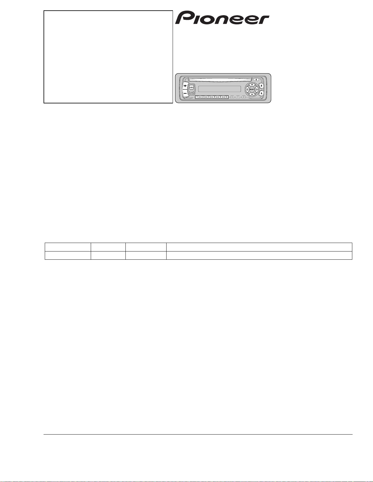
CRT2433
HIGH POWER CD PLAYER WITH FM/AM TUNER
DEH-1100 X1M/UC
CONTENTS
1. SAFETY INFORMATION ............................................2
2. EXPLODED VIEWS AND PARTS LIST.......................2
3. BLOCK DIAGRAM AND SCHEMATIC DIAGRAM .....8
4. PCB CONNECTION DIAGRAM ................................26
5. ELECTRICAL PARTS LIST ........................................36
6. ADJUSTMENT..........................................................41
7. GENERAL INFORMATION .......................................45
7.1 DIAGNOSIS ........................................................45
7.1.1 TEST MODE ..............................................45
7.1.2 DISASSEMBLY .........................................48
7.2 PARTS .................................................................52
7.2.1 IC................................................................52
7.2.2 DISPLAY....................................................58
7.3 OPERATIONAL FLOW CHART...........................59
8. OPERATIONS AND SPECIFICATIONS.....................60
DEH-11 X1M/UC
DEH-1100/X1M/UC
- This service manual should be used together with the following manual(s):
Model No. Order No. Mech. Module Remarks
CX-958 CRT2423 S8.1 CD Mech. Module:Circuit Description, Mech.Description, Disassembly
Page 2
2
DEH-1100,11
- CD Player Service Precautions
1. For pickup unit(CXX1285) handling, please refer
to"Disassembly"(see page 48).
During replacement, handling precautions shall be
taken to prevent an electrostatic discharge(protection
by a short pin).
2. During disassembly, be sure to turn the power off
since an internal IC might be destroyed when a con-
nector is plugged or unplugged.
3. Please checking the grating after changing the ser-
vice pickup unit(see page 43).
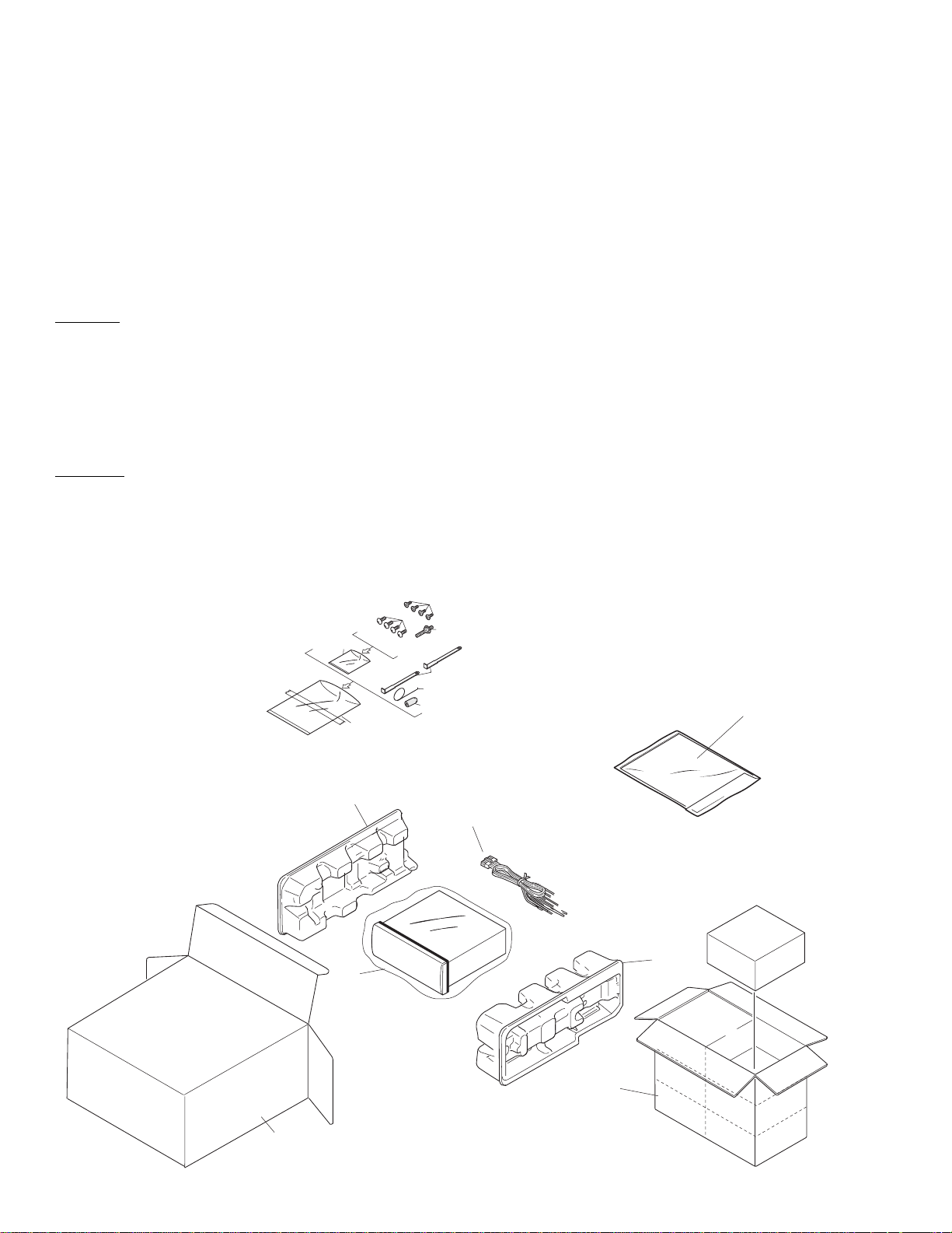
2. EXPLODED VIEWS AND PARTS LIST
2.1 PACKING
14
1
10
12
13
15
11
5
9
2
8
7
6
4
3
CAUTION
This service manual is intended for qualified service technicians; it is not meant for the casual do-it-yourselfer.
Qualified technicians have the necessary test equipment and tools, and have been trained to properly and safely repair
complex products such as those covered by this manual.
Improperly performed repairs can adversely affect the safety and reliability of the product and may void the warranty.
If you are not qualified to perform the repair of this product properly and safely; you should not risk trying to do so
and refer the repair to a qualified service technician.
W
ARNING
This product contains lead in solder and certain electrical parts contain chemicals which are known to the state of
California to cause cancer, birth defects or other reproductive harm.
Health & Safety Code Section 25249.6 - Proposition 65
1. SAFETY INFORMATION
Page 3
3
DEH-1100,11
1 Cord Assy CDE6124
2 Spring CBH1650
3 Screw CBA1002
* 4 Polyethylene Bag CEG-127
5 Screw CRZ50P090FMC
6 Screw TRZ50P080FMC
* 7 Polyethylene Bag CEG-158
8 Handle CNC5395
9 Bush CNV3930
10 Polyethylene Bag CEG1173
11-1 Polyethylene Bag CEG1116
11-2 Owner’s Manual CRD3133
11-3 Installation Manual CRD3134
* 11-4 Card ARY1048
12 Carton
See Contrast table(2)
13 Contain Box See Contrast table(2)
14 Protector CHP2243
15 Protector CHP2244
Mark No. Description Part No. Mark No. Description Part No.
(1) PACKING SECTION PARTS LIST
NOTE:
- Parts marked by “*” are generally unavailable because they are not in our Master Spare Parts List.
- Screws adjacent to ∇ mark on the product are used for disassembly.
Part No.
Mark No. Symbol and Description DEH-1100/X1M/UC DEH-11/X1M/UC
12 Carton CHG3953 CHG3954
13 Contain Box CHL3953 CHL3954
(2) CONTRAST TABLE
DEH-1100/X1M/UC and DEH-11/X1M/UC are constructed the same except for the following:
- Owner's Manual, Installation Manual
Model Part No. Language
DEH-1100/X1M/UC CRD3133 English, French, Spanish
DEH-11/X1M/UC CRD3134
Page 4
4
DEH-1100,11
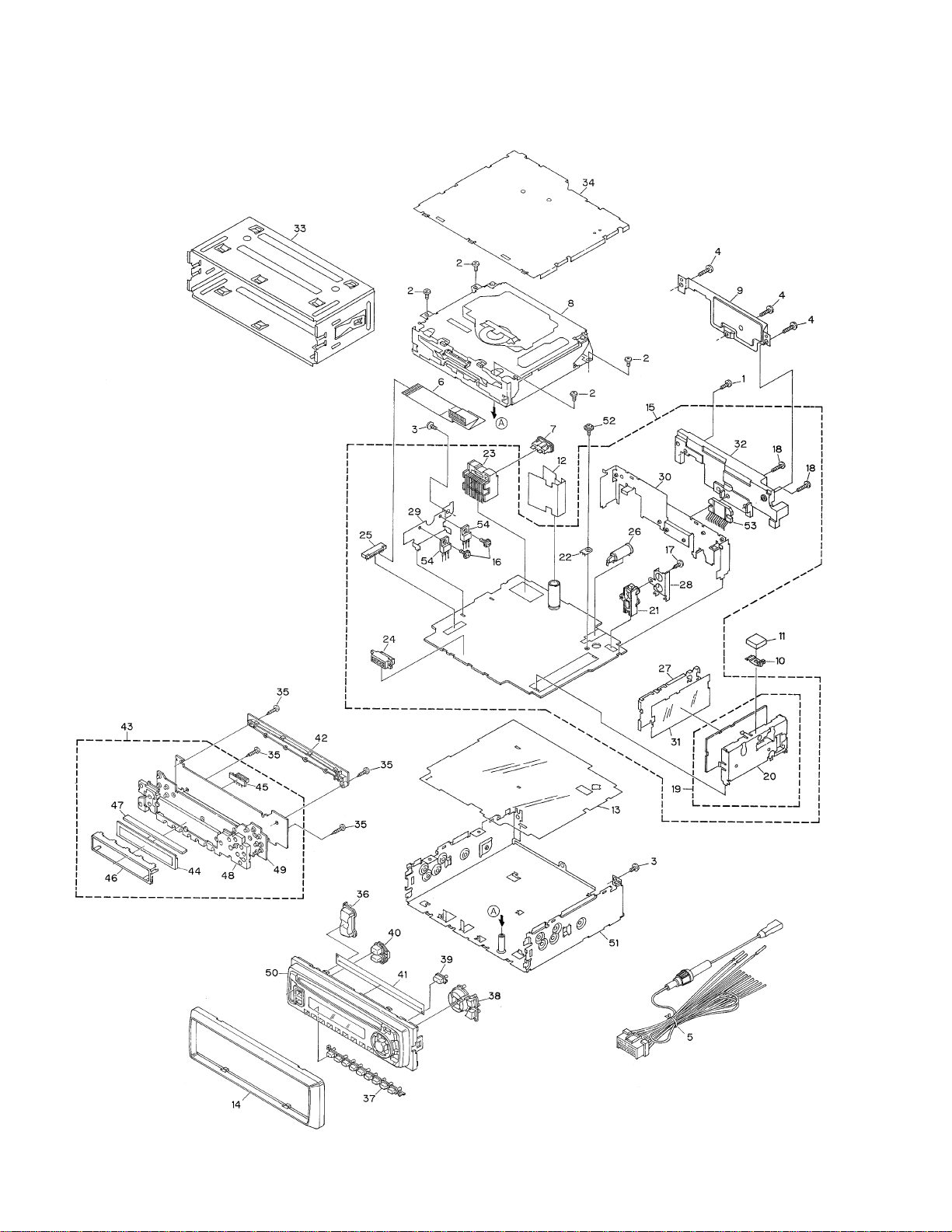
2.2 EXTERIOR
Page 5

5
DEH-1100,11
1 Screw BMZ26P120FMC
2 Screw BSZ26P060FMC
3 Screw BSZ30P060FMC
4 Screw BSZ30P120FMC
5 Cord Assy CDE6124
6 Cable CDE6160
7 Fuse(10A) CEK1136
8
CD Mechanism Module(S8.1) CXK5203
9 Cover CNC8367
10 Holder CNC8884
11 Spacer CNM4913
12 Insulator CNM6224
13 Insulator CNM6386
14 Panel CNS5132
15 Tuner Amp Assy CWM6769
16 Screw ASZ26P080FMC
17 Screw BPZ26P080FMC
18 Screw BSZ26P160FMC
19 FM/AM Tuner Unit CWE1501
20 Holder CNC7532
21 Pin Jack(CN301) CKB1041
22 Terminal(CN403) CKF1059
23 Connector(CN901) CKM1299
24 Connector(CN601) CKS3581
25 Connector(CN605) CKS3838
26 Antenna Jack(CN402) CKX1056
27 Holder CNC7533
28 Holder CNC8041
29 Holder CNC8043
30 Holder CNC8588
31 Insulator CNM5967
32 Heat Sink CNR1506
33 Holder Unit CXB2687
34 Case Unit CXB4033
35 Screw BPZ20P080FMC
36 Button(+, -) CAC6273
37 Button(1-6) CAC6275
38 Button(B, A, Cross) CAC6276
39 Button(Eject) CAC6277
40 Button(Source) CAC6495
41 Cover CNM6434
42 Holder CNV5963
43 Keyboard Unit
See Contrast table(2)
44 LCD(LCD1801) CAW1560
45 Connector(CN1801) CKS3580
46 Holder CNC8517
47 Rubber CNV5954
48 Lighting Conductor CNV5965
49 Rubber CNV5966
50 Grille Unit
See Contrast table(2)
51 Chassis Unit CXB4625
52 Screw ISS26P055FUC
53 IC(IC302) TDA7384
54 Transistor(Q904, 981) 2SD2396
(1) EXTERIOR SECTION PARTS LIST
Mark No. Description Part No. Mark No. Description Part No.
Part No.
Mark No. Symbol and Description DEH-1100/X1M/UC DEH-11/X1M/UC
43 Keyboard Unit CWM6783 CWM6782
50 Grille Unit CXB4619 CXB4620
(2) CONTRAST TABLE
DEH-1100/X1M/UC and DEH-11/X1M/UC are constructed the same except for the following:
Page 6
6
DEH-1100,11
2.3 CD MECHANISM MODULE
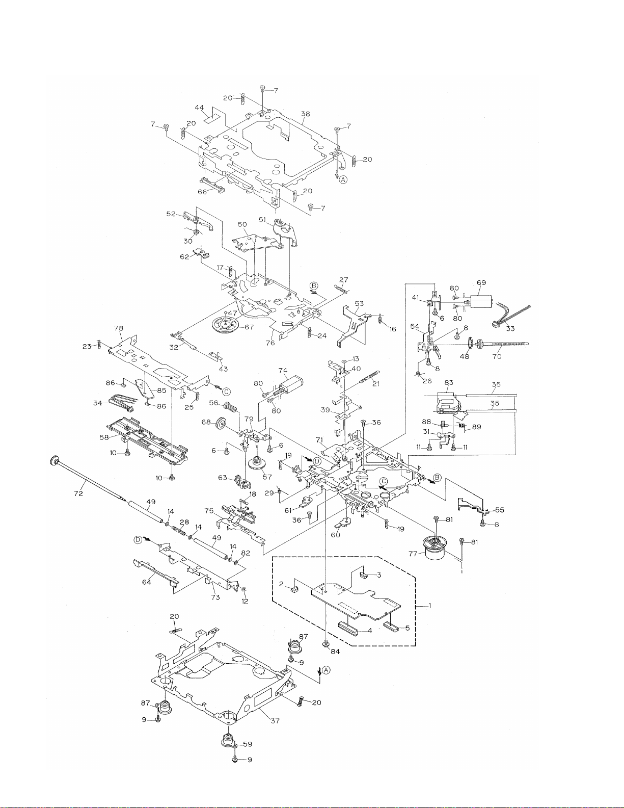
Page 7

7
DEH-1100,11
Mark No. Description Part No. Mark No. Description Part No.
1 Control Unit CWX2411
2 Connector(CN802) CKS2192
3 Connector(CN801) CKS2193
4 Connector(CN701) CKS2773
5 Connector(CN101) CKS3486
6 Screw BMZ20P030FMC
7 Screw BSZ20P040FMC
8 Screw(M2x3) CBA1077
9 Screw(M2x5) EBA1028
10 Screw CBA1243
11 Screw(M2x4) CBA1362
12 Washer CBF1037
13 Washer CBF1038
14 Washer CBF1060
15 •••••
16 Spring CBH2079
17 Spring CBH2117
18 Spring CBH2314
19 Spring CBH2110
20 Spring CBH2282
21 Spring CBH2318
22 •••••
23 Spring CBH2324
24 Spring CBH2118
25 Spring CBH2161
26 Spring CBH2163
27 Spring CBH2189
28 Spring CBH2249
29 Spring CBH2260
30 Spring CBH2262
31 Bracket CNC8568
32 Spring CBL1369
33 Connector CDE5531
34 Connector CDE5532
35 Shaft CLA3304
36 Screw(M2.6x6) CBA1458
37 Frame CNC8565
38 Frame CNC8749
39 Lever CNC7546
40 Arm CNC8663
41 Bracket CNC8567
42 •••••
43 Spacer CNM3315
44 Sheet CNM6659
45 •••••
46 •••••
47 Ball CNR1189
48 Belt CNT1086
49 Roller CNV4509
50 Arm CNV6037
51 Arm CNV5247
52 Arm CNV5248
53 Arm CNV5249
54 Guide CNV5254
55 Guide CNV5255
56 Gear CNV5257
57 Gear CNV5256
58 Guide CNV6176
59 Damper CNV6174
60 Arm CNV6096
61 Arm CNV6031
62 Arm CNV6211
63 Guide CNV6012
64 Guide CNV5510
65 •••••
66 Guide CNV5751
67 Clamper CNV6013
68 Gear CNV5813
69 Motor Unit(M1) CXB2190
70 Screw Unit CXB4726
71 Chassis Unit CXB4797
72 Gear Unit CXB4728
73 Arm Unit CXB4729
74 Motor Unit(M2) CXB2195
75 Lever Unit CXB4730
76 Arm Unit CXB4731
77 Motor Unit(M3) CXB2562
78 Arm Unit CXB4732
79 Bracket Unit CXB4795
80 Screw JFZ20P025FMC
81 Screw JGZ17P025FZK
82 Washer YE20FUC
83 Pickup Unit(Service)(P8) CXX1285
84 Screw IMS26P030FMC
* 85 PCB CNX2982
86 Photo-transistor(Q1, 2) CPT230SX-TU
87 Damper CNV6175
88 Rack CNV6014
89 Spring CBH2315
- CD MECHANISM MODULE SECTION PARTS LIST
Page 8
8
DEH-1100,11
1
23
4
1
234
D
C
B
A
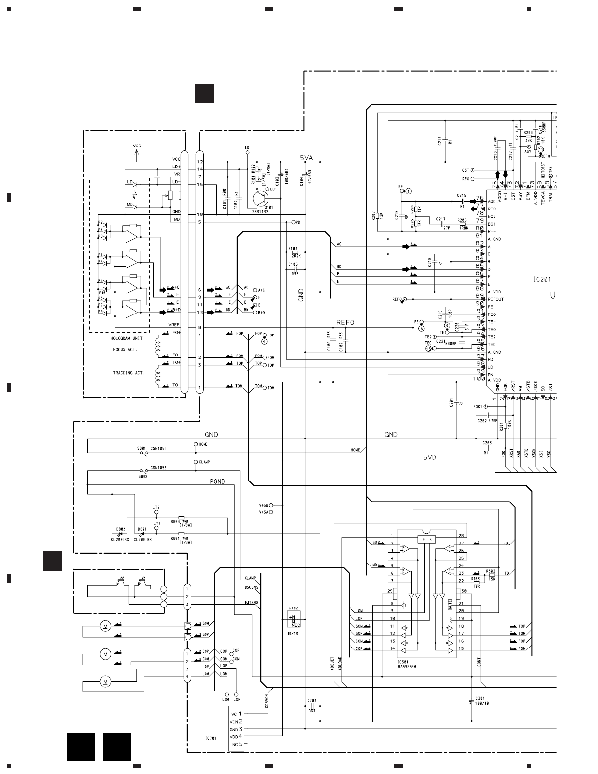
3. BLOCK DIAGRAM AND SCHEMATIC DIAGRAM
3.1 BLOCK DIAGRAM
ANT1 TV
ANT2 TV
RF TV
IC 3
BR9010FV
AM 2ND IF 450kHz
M
M
M
LD
MD
HOLOGRAM
UNIT
FOCUS ACT
TRACKING ACT
LD+
MD
FO+
TO+
14
5
4
3
SPINDLE
MOTOR
CARRIAGE
MOTOR
LOADING
MOTOR
1
2
3
4
3
1
2
SELECT
SENSE
DISC SENSE
E
CN801
CN802
D803 D802 D801
VD
S802
CLAMP
6
5
11
22
23
21
1
28
21
CDLOAD
CDEJET
CONT
EJTSNS
DSCSNS
CLAMP
CD5VON
VDCONT
VDD
IC 701
BA05SFP
IN
+5V REGULATOR
24
1
VD
Q981
Q982
B.U
ANTENNA
CN402
A
B
27
28
FM FRONT END
Q3
Q201 Q204
AM RF
FM/AM 1ST IF 10.7MHz
T51 Q51 CF51 CF52 CF53
MIXER.IF AMP DET
IC 1
PML002A
38 39 42 44 46 63
32 19
46
6
21
18
LDET
COMP
34 33 41 44 11 12 13
69
70
54
78
65
71
75746157554533
35
22
2225 10 14 12 15 16 13 2 3 4
CF202
VDD
LOCL
VCC
Q411
VCC
VDD
DI/DO
CE2CKCE1SLFMSD
PCE2CKPCE1
PCK
SD
PDIO
NL1
NL2
EEPROM
5
6
4
3
IC 2 PM4008A
FM MPX
D
Q101
CN101
FOP
TOP
A+C/F
B+D/E
98
LD L_OUT
PD
HOME
97
24
23
39
X201
TD/FD
SD/MD
RF-AMP, DSP,
SERVO, DAC
IC 201
UPD63711GC
16
CN701 CN605
1718
24
CDL
IC 301
BA5985FM
S801
HOME
12
16
18
11
14
13
10
9
SOP
TOP
FOP
SOM
COP
COM
LOP
LOM
FWD
REV
MUTE
25 24
CD DRIVER
718
19
20
14
3
2
4
CLAMP
DINC
EJTD
CDLOAD
EJET
CONT
Q202
32
PD
TUNER AMP ASSY
FM/AM TUNER UNIT
CONTROL UNIT
PICKUP UNIT(SERVICE)(P8)
PHOTO UNIT(S8)
4
VD
CD5VON
Page 9
9
DEH-1100,11
5
6
78
5
6
7
8
D
C
B
A
KYDT
DPDT
LCD DRIVER
IC 1801
PD6293A
3
4
5
3
4
5
KEY MATRIX
SD
SL
TUNPCE
TUNPCK
TUNPCE2
TUNPDO
LOCL
IN1
IN2
6
76
14
13
48
12
67
2
3
SYSTEM
CONTROLLER
IC 601(1/2)
PE5091A
VST
VCK
VDT
B.U
VDD
Q903
B.U
BACKUP
FL–
FL+
RL–
RL+
ACC
2
1
9
11
10
12
4
ELECTRONIC VOLUME/
SOURCE SELECTOR
IC 301
SN761029DL
SYSTEM
CONTROLLER
IC 601(2/2)
PE5091A
ASENS
63
BSENS
64
SYSPW
42
MUTE
44
KYDT
8
DPDT
9
RESET
60
SWVDD
41
Fout
19
Rout
20
POWER AMP
IC 302
TDA7384
14
12
22 4
5
3
21
23
FL
MUTE STBY
RL
B.U
bsens
asens
Q902
Q351 MUTE
C
KEYBOARD UNIT
CN1801
CN601
LCD
22 23
X1801
20
18
Q650
RESET
IC 602
S–80834ANY
VDD
12
SYSPW
BACK UP
GND
FL–
FL+
RL–
RL+
5
B.REMOTE
FUSE
10A
GND
ACC
B.REMOTE
CD5VON
31
34
23
80
79
27
22
35
VDCONT
CLAMP
DSCSNS
EJTSNS
CDLOAD
CDEJECT
CONT
TUNPDI
11
PDIO
VST/ VCK/ VDT
Q901
VDD
VDD
VLCD
50
10
Q346
CN301
REAR L CH
Q353
Q942 Q941
Page 10
10
DEH-1100,11
1
23
4
1
234
D
C
B
A
3.2 OVERALL CONNECTION DIAGRAM(GUIDE PAGE)
Note: When ordering service parts, be sure to refer to “EXPLODED VIEWS AND PARTS LIST” or “ELECTRICAL PARTS
LIST”.
A-a
A-b
A-b
A-a
A
A-a
DSP-201M-S00B
C499
103
272
272
183
183
162 162
104
4.194304MHz
CSS1023
104
433 822
682
R699 0R0
150 150
FM(100%):-19.5dBs
AM (30%):-30dBs
CD:+4.
FM(100%):-19
AM (30%):-30
FM/AM TUNER UNIT
For resistors and capacitors in the circuit diagrams, their resistance values or
capacitance values are expressed in codes:
Ex. *Resistors
Code Practical value
123 12k ohms
103 10k ohms
*Capacitors
Code Practical value
103 0.01µF
101/10 100µF/10V
The > mark found on some component parts indicates
the importance of the safety factor of the part.
Therefore, when replacing, be sure to use parts of
identical designation.
Symbol indicates a resistor.
No differentiation is made between chip resistors and
discrete resistors.
NOTE :
Symbol indicates a capacitor.
No differentiation is made between chip capacitors and
discrete capacitors.
R
SYSTEM CONTROLLER
KEYBOARD
UNIT
B
C
Large size
A-b
A-b
SCH diagram
Guide page
Detailed page
A-a A-b
A-a
A-a
Page 11

11
DEH-1100,11
5
6
78
5
6
7
8
D
C
B
A
A-b
A
332/16
600µH
>
(B2)
CEK1136
9.5dBs
CD:+10.1dBs
FM(100%):+3.5dBs
AM (30%):-7dBs
CD:+10.1dBs
FM(100%):+3.5dBs
AM (30%):-7dBs
CD:+36.1dBs
FM(100%):+29.5dBs
AM (30%):+19dBs
CD:+4.1dBs
CD MECHANISM MODULE
POWER AMP
SOURCE SELECTOR/
E.VOL
Reset
VD REGULATOR
TUNER AMP ASSY
A
A
D
Page 12
12
DEH-1100,11
1
23
4
1
234
D
C
B
A
A-a
A-a
A-b
DSP-201M-S00B
C499
103
272
272
183
183
162 162
104
4.194304MHz
CSS1023
150 150
FM(100%):-19.5dBs
AM (30%):-30dBs
CD:+4.1dBs
FM(100%):-19.5dBs
AM (30%):-30dBs
FM/AM TUNER UNIT
SOURCE
E.VOL
B
1
Page 13
13
DEH-1100,11
5
6
78
5
6
7
8
D
C
B
A
A-a
A-a
A-b
104
433 822
682
R699 0R0
150 150
CD MECHANISM MODULE
For resistors and capacitors in the circuit diagrams, their resistance values or
capacitance values are expressed in codes:
Ex. *Resistors
Code Practical value
123 12k ohms
103 10k ohms
*Capacitors
Code Practical value
103 0.01µF
101/10 100µF/10V
The > mark found on some component parts indicates
the importance of the safety factor of the part.
Therefore, when replacing, be sure to use parts of
identical designation.
Symbol indicates a resistor.
No differentiation is made between chip resistors and
discrete resistors.
NOTE :
Symbol indicates a capacitor.
No differentiation is made between chip capacitors and
discrete capacitors.
Reset
SYSTEM CONTROLLER
KEYBOARD
UNIT
C
D
2
Page 14
14
DEH-1100,11
1
23
4
1
234
D
C
B
A
A-a
A-b
A-b
332/16
600µH
>
CEK1136
CD:+10.1dBs
FM(100%):+3.5dBs
AM (30%):-7dBs
CD:+10.1dBs
FM(100%):+3.5dBs
AM (30%):-7dBs
CD:+36.1dBs
FM(100%):+29.5dBs
AM (30%):+19dBs
POWER AMP
SOURCE SELECTOR/
E.VOL
TUNER AMP ASSY
A
A
1
Page 15
15
DEH-1100,11
5
6
78
5
6
7
8
D
C
B
A
A-b
A-a
A-b
600µH
(B2)
CD:+4.1dBs
CD MECHANISM MODULE
VD REGULATOR
D
2
Page 16
16
DEH-1100,11
1
23
4
1
234
D
C
B
A
B
KV1410(23)
Mark
None
F0
F65
F125
A0
A74
A125
Band
–
FM
FM
FM
AM
AM
AM
Input Level
–
0dBf
65dBf
125dBf
0dBµ
74dBµ
125dBµ
DAN217U
DAN217U
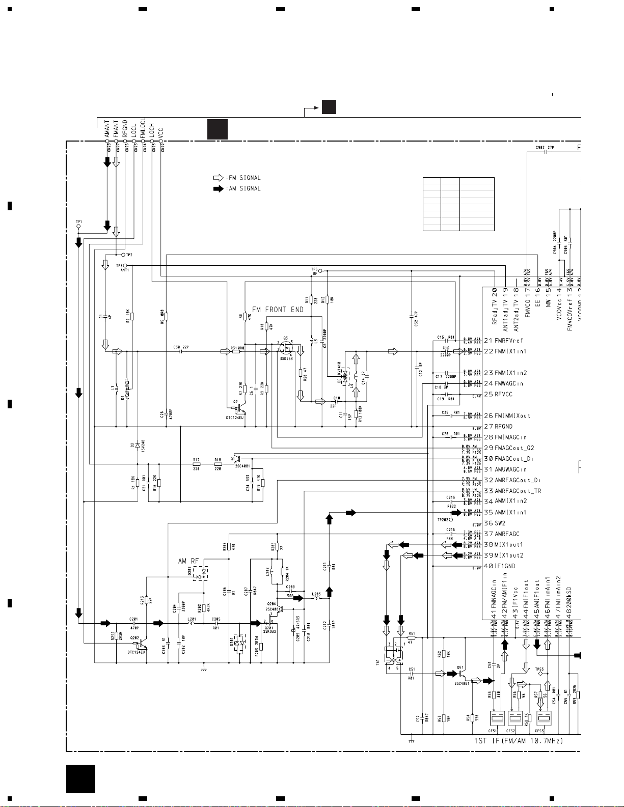
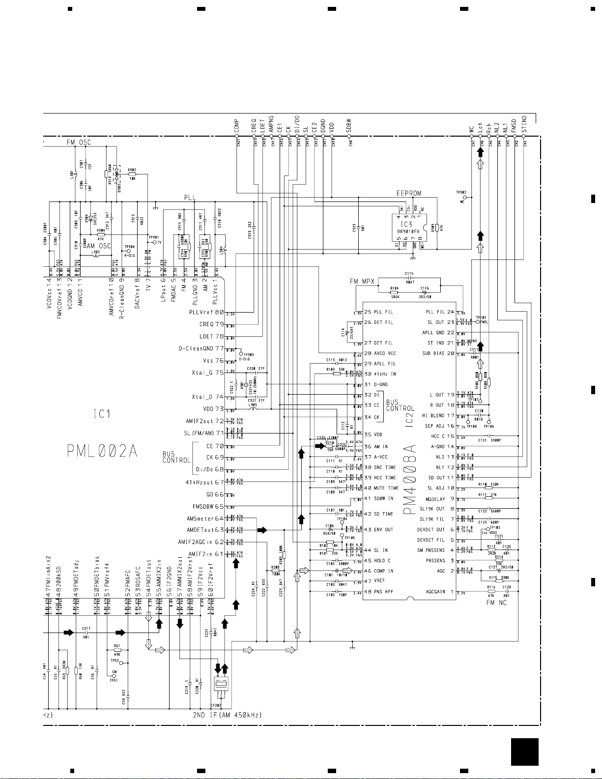
3.3 FM/AM TUNER UNIT
FM/AM TUNER UNIT
B
A
Page 17
17
DEH-1100,11
5
6
78
5
6
7
8
D
C
B
A
KV1410(23)
B
Page 18
18
DEH-1100,11
1
23
4
1
234
D
C
B
A
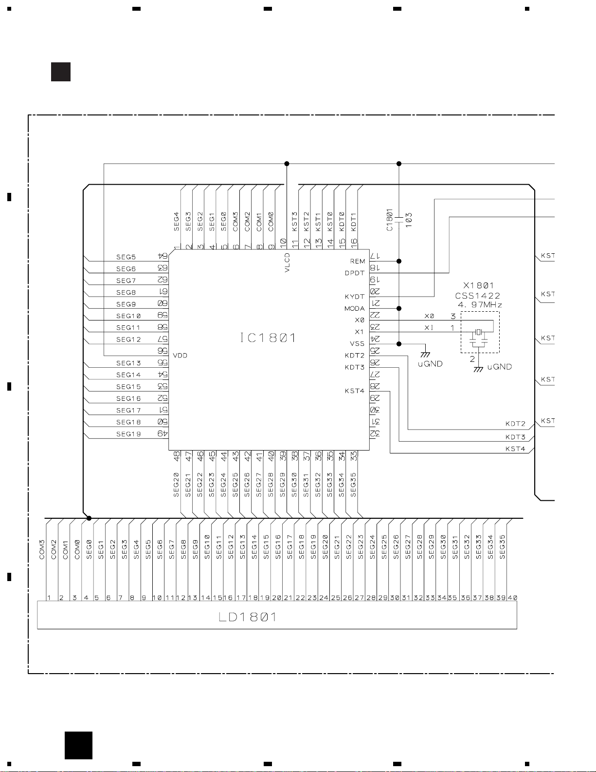
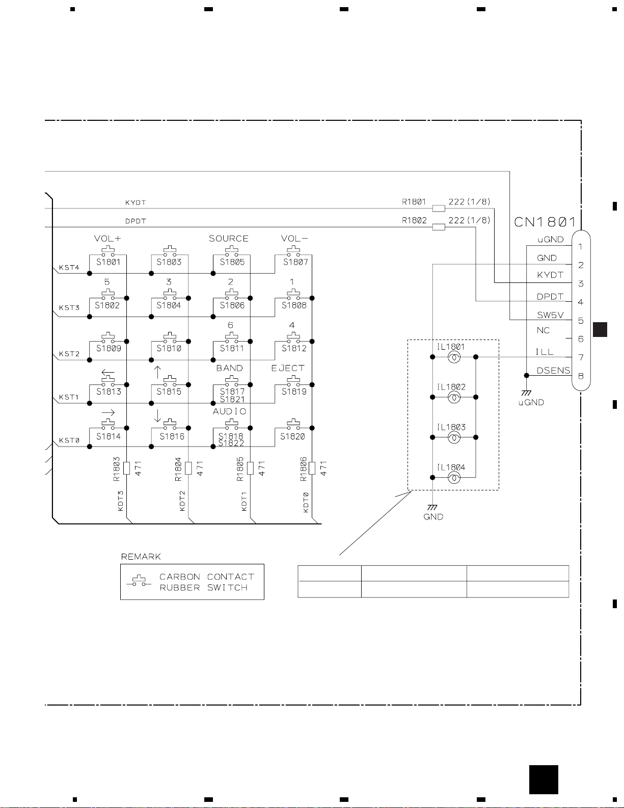
3.4 KEYBOARD UNIT
KEYBOARD UNIT
C
LCD DRIVER,
KEY CONTROLLER
PD6293A
CAW1560
C
Page 19
19
DEH-1100,11
5
6
78
5
6
7
8
D
C
B
A
C
LOUD
CLK
LOCAL
BSM
DEH-1100/X1M/UC DEH-11/X1M/UC
IL1801-1804 CEL1547(14V 40mA) CEL1638(14V 40mA)
CN601
A
Page 20
DEH-1100,11
1
23
4
1
234
D
C
B
A
BA05SFP
(SERVICE)(P8)
PICKUP UNIT
PHOTO UNIT(S8)
CONTROL UNIT
SPINDLE MOTOR
Q2 CPT230SX-TUQ1 CPT230SX-TU
M3 CXB2562
CARRIAGE MOTOR
M1 CXB2190
M2 CXB2195
LOADING MOTOR
RF-AMP, SE
5V REGULATOR
CD DRIVER
CN101
CN802
CN801
3.5 CD MECHANISM MODULE
E
D
20
D
E
Page 21

DEH-1100,11
5
6
78
5
6
7
8
D
C
B
A
SWITCHES:
CONTROL UNIT
S801 : HOME SWITCH.....ON-OFF
S802 : CLAMP SWITCH....ON-OFF
The underlined indicates the switch position.
CN701
CN605
D
21
A
Page 22

22
DEH-1100,11
1 RFI 0.5V/div. 0.5µs/div.
Normal mode: play
1 CH1: RFI 1V/div.
2 CH2: MIRR 5V/div.
Test mode: Tracking open
0.5ms/div.
1 CH1: RFI 1V/div.
2 CH2: MIRR 5V/div.
Normal mode: The defect part
passes 800µm
0.5ms/div.
3 CH1: FD 0.5V/div.
4 CH2: FO+ 2V/div.
Test mode: No disc, Focus close
0.2s/div.
3 CH1: FD 0.5V/div.
5 CH2: FOK 2V/div.
Normal mode: Focus close
0.2s/div.
6 CH1: FE 0.5V/div.
7 CH2: XSI 2V/div.
Normal mode: Focus close
1ms/div.
REFO
→
8 CH1: TE 0.5V/div.
9 CH2: TD 0.5V/div.
Test mode: 32 tracks jump (FWD)
0.5ms/div.
8 CH1: TE 0.5V/div.
9 CH2: TD 0.5V/div.
Test mode: Single jump (FWD)
0.5ms/div.
8 CH1: TE 0.5V/div.
9 CH2: TD 0.5V/div.
Test mode: 100 tracks jump (FWD)
5ms/div.
6 CH1: FE 0.1V/div.
3 CH2: FD 0.2V/div.
Normal mode: Play
20ms/div.
3 CH1: FD 0.5V/div.
0 CH2: MD 1V/div.
Normal mode: Focus close (12cm)
0.5s/div.
3 CH1: FD 0.5V/div.
0 CH2: MD 1V/div.
Normal mode: Focus close (8cm)
0.5s/div.
REFO
→
REFO
→
REFO
→
REFO
→
REFO
→
REFO
→
GND
→
REFO
→
REFO
→
REFO
→
REFO
→
REFO
→
REFO
→
REFO
→
REFO
→
REFO
→
REFO
→
REFO
→
REFO
→
- Waveforms
Note:1. The encircled numbers denote measuring pointes in the circuit diagram.
2. Reference voltage
REFO:2.5V
REFO
→
REFO
→
REFO
→
REFO
→
Page 23

23
DEH-1100,11
8 CH1: TE 0.2V/div.
9 CH2: TD 0.2V/div.
Normal mode: play
8 CH1: TE 0.5V/div.
! CH2: SD 0.5V/div.
TEST mode: 100 Tracks jump(FWD)
5ms/div.
0 MD 0.5V/div. 0.1s/div.
Normal mode: Play (12cm)
0 MD 1V/div. 10ms/div.
Normal mode:
Long Search (12cm)
@ EFM 1V/div. 5µs/div.
Normal mode: play
8 CH1: TE 1V/div.
# CH2: TEC 1V/div.
Test mode: Focus close
Tracking open
2ms/div.
8 CH1: TE 0.5V/div.
6 CH2: FE 0.5V/div.
Normal mode:
AGC after focus close
0.2s/div.
$ PLCK 2V/div. 0.5µs/div.
Normal mode: play
20ms/div.
% SCKO 2V/div. 1µs/div.
Normal mode: play
^ Dout 2V/div. 10µs/div.
Normal mode: play
& LRCK 2V/div. 20µs/div.
Normal mode: play
* VD 5V/div. 50ms/div.
Normal mode: No disc
GND
→
REFO
→
REFO
→
GND
→
REFO
→
REFO
→
REFO
→
REFO
→
REFO
→
REFO
→
REFO
→
REFO
→
REFO
→
GND
→
REFO
→
GND
→
REFO
→
GND
→
REFO
→
GND
→
REFO
→
Page 24

24
DEH-1100,11
( CH1: R OUT 1V/div.
) CH2: L OUT 1V/div.
Normal mode: Play (1kHz 0dB)
6 CH1: FE 0.2V/div.
3 CH2: FD 0.5V/div.
Normal mode: During AGC
1ms/div.
8 CH1: TE 0.2V/div.
9 CH2: TD 0.5V/div.
Normal mode: During AGC
1 CH1: RFI 1V/div.
⁄ CH2: HOLD 5V/div.
Normal mode: The defect part passes
800µm(B.D)
0.2ms/div. 1ms/div.
0.5ms/div.
3 CH1: FD 0.5V/div.
⁄ CH2: HOLD 5V/div.
Normal mode: The defect part passes
800µm(B.D)
0.5ms/div.
9 CH1: TD 0.1V/div.
⁄ CH2: HOLD 5V/div.
Normal mode: The defect part passes
800µm(B.D)
0.5ms/div.
REFO
→
REFO
→
REFO
→
REFO
→
REFO
→
REFO
→
REFO
→
REFO
→
REFO
→
REFO
→
REFO
→
REFO
→
Page 25

25
DEH-1100,11
Page 26

26
DEH-1100,11
1
23
4
1
234
D
C
B
A
4. PCB CONNECTION DIAGRAM
4.1 TUNER AMP ASSY
NOTE FOR PCB DIAGRAMS
1. The parts mounted on this PCB
include all necessary parts for
several destination.
For further information for
respective destinations, be sure
to check with the schematic dia-
gram.
2. Viewpoint of PCB diagrams
A
CORD ASSY
CN701
CN1801
TUNER AMP ASSY
Connector
P.C.Board
Capacitor
Chip Part
SIDE A
SIDE B
A
D
C
Page 27

27
DEH-1100,11
5
6
78
5
6
7
8
D
C
B
A
A
SIDE A
B
Page 28

28
DEH-1100,11
1
23
4
1
234
D
C
B
A
A
TUNER AMP ASSY
A
Page 29

29
DEH-1100,11
5
6
78
5
6
7
8
D
C
B
A
A
SIDE B
Page 30

30
DEH-1100,11
1
23
4
1
234
D
C
B
A
4.2 FM/AM TUNER UNIT
SIDE A
FM/AM TUNER UNIT
B
A
B
Page 31

31
DEH-1100,11
1
2
34
1
2
3
4
D
C
B
A
SIDE B
FM/AM TUNER UNIT
B
B
Page 32

32
DEH-1100,11
1
23
4
1
234
D
C
B
A
4.3 KEYBOARD UNIT
C
SIDE A
KEYBOARD UNIT
+
LOUD
1 2 3 4 5 6 LOCAL CLOCK BSM
BAND
EJECT
'
][
'
AUDIO
SOURCE/OFF
-
C
Page 33

33
DEH-1100,11
1
2
34
1
2
3
4
D
C
B
A
C
SIDE B
KEYBOARD UNIT
CN601
A
C
Page 34

34
DEH-1100,11
1
23
4
1
234
D
C
B
A
4.4 CD MECHANISM MODULE
CONTROL UNIT
HOME
M1 CARRIAGE MOTOR
M2 LOADING MOTOR
M3 SPINDLE MOTOR
PICKUP UNIT(SERVICE)(P8)
CN802
CN605
321
PHOTO UNIT(S8)
SIDE A
D
E
E
A
D
E
D
Page 35

35
DEH-1100,11
1
2
34
1
2
3
4
D
C
B
A
SIDE B
CONTROL UNIT
D
CLAMP
D
Page 36

36
DEH-1100,11
5. ELECTRICAL PARTS LIST
NOTES:
- Parts whose parts numbers are omitted are subject to being not supplied.
- The part numbers shown below indicate chip components.
Chip Resistor
RS1/_S___J,RS1/__S___J
Chip Capacitor (except for CQS.....)
CKS....., CCS....., CSZS.....
=====Circuit Symbol and No.===Part Name Part No.
--- ------ ------------------------------------------ -------------------------
Unit Number : CWM6769
Unit Name : Tuner Amp Assy
MISCELLANEOUS
IC 301 IC SN761029DL
IC 302 IC TDA7384
IC 601 IC PE5091A
IC 602 IC S-80834ANY
Q 346 Transistor RN1610
Q 351 Transistor DTC114EK
Q 353 Transistor DTA124EK
Q 411 Transistor 2SC2412K
Q 650 Transistor 2SA1037K
Q 901 Transistor 2SC2412K
Q 902 Transistor 2SC2412K
Q 903 Transistor 2SD1859
Q 904 Transistor 2SD2396
Q 905 Transistor 2SB1243
Q 906 Transistor DTC114EK
Q 941 Transistor 2SB1243
Q 942 Transistor DTC114EK
Q 981 Transistor 2SD2396
Q 982 Transistor RN46A1
D 901 Diode HZS7L(C2)
D 902 Diode S5688G
D 903 Diode S5688G
D 904 Diode HZS7L(A1)
D 905 Diode S5688G
D 906 Diode HZS6L(B2)
D 907 Diode HZS9L(B3)
D 941 Diode S5688G
D 942 Diode S5688G
D 981 Diode HZS9L(B1)
L 401 Ferri-Inductor LAU4R7K
L 402 Ferri-Inductor LAU2R2K
L 403 Inductor LAU100K
L 610 Ferri-Inductor LAU101K
L 611 Ferri-Inductor LAU2R2K
L 650 Ferri-Inductor LAU2R2K
L 901 Choke Coil 600µH CTH1221
TH 601 Thermistor CCX1031
X 610 Crystal Resonator 4.194304MHz CSS1023
AR 946 Arrester DSP-201M-S00B
FM/AM Tuner Unit CWE1501
RESISTORS
R 310 RD1/4PU222J
R 311 RD1/4PU222J
R 312 RS1/10S272J
R 313 RS1/10S272J
R 314 RS1/10S151J
R 315 RS1/10S151J
R 316 RS1/10S0R0J
R 317 RS1/10S121J
R 318 RD1/4PU104J
R 319 RD1/4PU104J
R 320 RS1/10S121J
R 321 RS1/10S101J
R 322 RS1/10S101J
R 342 RS1/8S821J
R 343 RS1/8S821J
R 344 RS1/10S223J
R 345 RS1/10S223J
R 352 RS1/10S103J
R 353 RS1/10S103J
R 354 RS1/10S331J
R 360 RD1/4PU153J
R 411 RS1/10S681J
R 412 RS1/10S681J
R 413 RS1/10S681J
R 414 RS1/10S103J
R 415 RS1/8S681J
R 416 RD1/4PU473J
R 417 RD1/4PU472J
R 418 RS1/10S473J
R 419 RS1/10S473J
R 420 RS1/10S473J
R 421 RS1/10S473J
R 422 RS1/10S473J
R 423 RS1/10S681J
R 424 RS1/10S681J
R 425 RS1/10S393J
R 427 RS1/10S222J
R 428 RS1/10S222J
R 460 RS1/10S272J
R 461 RS1/10S272J
R 464 RS1/10S162J
R 465 RS1/10S162J
R 468 RS1/10S0R0J
R 469 RS1/10S0R0J
R 610 RD1/4PU822J
R 611 RS1/10S433J
R 614 RS1/8S0R0J
R 619 RS1/10S682J
R 620 RN1/10SE2202D
R 622 RD1/4PU222J
R 623 RD1/4PU222J
R 624 RS1/10S473J
R 625 RS1/10S473J
R 626 RS1/10S473J
R 627 RD1/4PU473J
R 628 RD1/4PU222J
R 629 RS1/10S473J
R 630 RS1/10S822J
R 649 RS1/8S222J
R 650 RS1/8S222J
=====Circuit Symbol and No.===Part Name Part No.
--- ------ ------------------------------------------ -------------------------
A
Page 37

37
DEH-1100,11
R 651 RS1/8S222J
R 655 RS1/10S103J
R 656 RS1/10S103J
R 657 RD1/4PU102J
R 658 RD1/4PU102J
R 660 RS1/10S1R0J
R 681 RD1/4PU681J
R 682 RS1/10S102J
R 683 RD1/4PU102J
R 684 RS1/10S102J
R 699 RS1/10S0R0J
R 725 RS1/10S0R0J
R 901 RS1/10S473J
R 902 RD1/4PU103J
R 903 RD1/4PU103J
R 904 RS1/10S473J
R 905 RS1/10S102J
R 906 RS1/10S473J
R 907 RS1/10S473J
R 908 RS1/10S472J
R 909 RD1/4PU103J
R 911 RS1/10S122J
R 912 RD1/4PU103J
R 914 RD1/4PU152J
R 916 RS1/10S221J
R 918 RS1/10S1R0J
R 941 RD1/4PU472J
R 942 RD1/4PU152J
R 981 RS1/10S472J
R 982 RS1/10S222J
R 983 RD1/4PU221J
R 984 RD1/4PU221J
CAPACITORS
C 310 CKSQYB105K16
C 311 CKSQYB104K16
C 312 CEJA2R2M50
C 313 CKSQYB105K16
C 314 CKSYB104K16
C 315 CKSQYB102K50
C 316 CKSQYB102K50
C 317 CEJA100M16
C 318 CEJA100M16
C 319 CKSQYB822K50
C 320 CKSQYB822K50
C 321 CEAL1R0M50
C 322 CEJA1R0M50
C 323 CKSQYB183K50
C 324 CKSQYB183K50
C 325 CKSQYB104K16
C 326 CKSQYB104K16
C 327 CKSQYB104K16
C 328 CKSQYB104K16
C 329 CEJA2R2M50
C 330 CEJA4R7M50
C 332 CKSQYB473K16
C 333 CKSQYB104K16
C 334 CKSQYB104K16
C 335 CEAL470M10
C 340 CEAL2R2M50
C 341 CEJA2R2M50
C 350 CEJA330M10
C 361 CEJA2R2M50
C 362 CKSYB225K16
C 363 CEJA100M16
C 364 CKSYB474K16
C 365 CKSQYB474K16
C 366 CKSYB474K16
C 367 CKSQYB474K16
C 368 CKSQYB474K16
C 369 CKSYB474K16
C 370 CKSQYB474K16
C 371 CKSYB474K16
C 372 CKSQYB225K10
C 390 CKSQYB104K16
C 391 3300µF/16V CCH1368
C 411 CKSQYB223K25
C 412 CKSQYB223K25
C 413 CKSQYB102K50
C 414 CEJA220M10
C 415 CKSQYB473K16
C 416 CEAL101M10
C 417 CKSQYB472K50
C 462 CKSQYB183K25
C 463 CKSQYB183K25
C 490 CKSQYB103K50
C 499 CKSQYB103K50
C 611 CKSQYB104K16
C 612 CEJA4R7M35
C 613 CKSQYB473K16
C 614 CKSQYB102K50
C 628 CCSQCH150J50
C 629 CCSQCH150J50
C 630 CKSQYB473K16
C 631 CEAL2R2M50
C 650 CKSQYB104K16
C 901 CEJA101M10
C 902 CKSQYB473K16
C 903 470µF/16V CCH1331
C 904 CKSQYB473K16
C 905 330µF/16V CCH1326
C 906 CKSQYB103K50
C 907 CEJA101M16
C 941 CKSQYB473K16
C 981 CEJA101M10
C 982 CKSQYB102K50
C 983 CKSQYB473K16
Unit Number : CWE1501
Unit Name : FM/AM Tuner Unit
MISCELLANEOUS
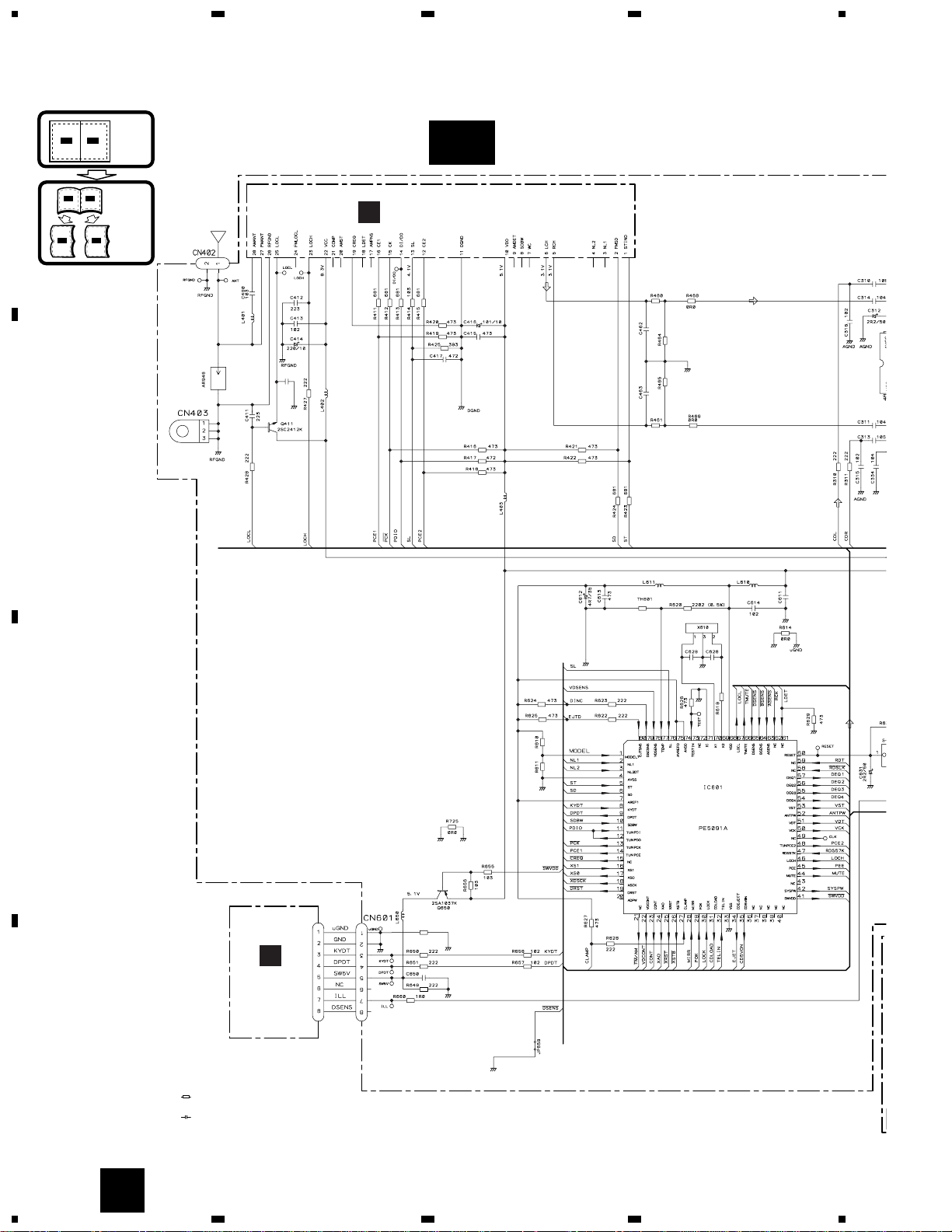
IC 1 IC PML002A
IC 2 IC PM4008A
IC 3 IC BR9010FV
Q 1 Transistor 2SC4081
Q 2 Transistor DTC124EU
Q 3 FET 3SK263
Q 51 Transistor 2SC4081
Q 201 FET 2SK932
Q 202 Transistor DTC124EU
Q 204 Transistor 2SC4081
D 1 Diode KV1410(23)
D 2 Diode 1SV248
D 6 Diode KV1410(23)
D 201 Diode DAN217U
D 202 Diode DAN217U
D 903 Diode KV1410(23)
D 904 Diode SVC253
L 1 Coil CTC1155
L 3 Inductor LCTB1R5K2125
L 4 Coil CTC1155
=====Circuit Symbol and No.===Part Name Part No.
--- ------ ------------------------------------------ -------------------------
=====Circuit Symbol and No.===Part Name Part No.
--- ------ ------------------------------------------ -------------------------
B
Page 38

38
DEH-1100,11
L 201 Inductor LCTB330K1608
L 202 Inductor CTF1287
L 203 Inductor LCTA121J3225
L 901 Coil CTC1154
L 902 Inductor LCTA3R3J3225
L 904 Inductor LCTBR47K1608
L 905 Inductor LCTBR47K1608
T 51 Coil CTE1132
CF 51 Ceramic Filter CTF1442
CF 52 Ceramic Filter CTF1442
CF 53 Ceramic Filter CTF1442
CF 202 Ceramic Filter CTF1348
X 901 Crystal Resonator 10.250MHz CSS1432
RESISTORS
R 1 RS1/16S183J
R 2 RS1/16S103J
R 5 RS1/16S0R0J
R 7 RS1/16S273J
R 8 RS1/16S473J
R 9 RS1/16S223J
R 10 RS1/16S473J
R 11 RS1/16S221J
R 12 RS1/16S103J
R 13 RS1/16S104J
R 16 RS1/16S223J
R 17 RS1/16S221J
R 18 RS1/16S221J
R 19 RS1/16S473J
R 20 RS1/16S470J
R 31 RS1/16S0R0J
R 51 RS1/16S470J
R 52 RS1/16S103J
R 53 RS1/16S103J
R 54 RS1/16S331J
R 55 RS1/16S331J
R 56 RS1/16S560J
R 57 RS1/16S560J
R 58 RS1/16S102J
R 59 RS1/16S225J
R 60 RS1/16S133J
R 61 RS1/16S433J
R 101 RS1/16S333J
R 102 RS1/16S103J
R 103 RS1/16S333J
R 104 RS1/16S562J
R 106 RS1/16S0R0J
R 108 RS1/16S0R0J
R 110 RS1/16S154J
R 111 RS1/16S273J
R 113 RS1/16S222J
R 114 RS1/16S333J
R 115 RS1/16S334J
R 116 RS1/16S473J
R 202 RS1/16S472J
R 203 RS1/16S225J
R 204 RS1/16S102J
R 205 RS1/16S220J
R 206 RS1/16S471J
R 208 RS1/16S104J
R 209 RS1/16S104J
R 210 RS1/16S563J
R 213 RS1/16S223J
R 251 RS1/16S225J
R 902 RS1/16S103J
R 904 RS1/16S473J
R 907 RS1/16S103J
R 908 RS1/16S681J
R 909 RS1/16S473J
R 914 RS1/16S562J
CAPACITORS
C 1 CCSQCH4R0C50
C 6 CKSQYB105K10
C 8 CKSRYB222K50
C 10 CCSRCH220J50
C 11 CCSRCH150J50
C 12 CCSRCH8R0D50
C 14 CCSRCJ3R0C50
C 15 CKSRYB103K50
C 16 CKSRYB222K50
C 17 CKSRYB222K50
C 18 CCSRCJ3R0C50
C 19 CKSRYB103K50
C 20 CKSRYB103K50
C 21 CKSRYB103K50
C 24 CKSQYB334K16
C 26 CKSRYB472K50
C 30 CCSRCH220J50
C 32 CCSRCH470J50
C 35 CKSRYB103K50
C 51 CKSRYB103K50
C 52 CKSRYB473K16
C 53 CCSRCK2R0C50
C 54 CKSRYB103K50
C 55 CKSRYB104K16
C 56 CKSRYB104K16
C 58 CKSQYB224K16
C 101 CEALNP100M10
C 102 CCSRCH151J50
C 103 CKSRYB473K16
C 105 CKSRYB682K25
C 106 CEALR68M50
C 107 CKSRYB103K50
C 108 CKSQYB474K16
C 109 CKSQYB474K16
C 110 CKSRYB104K16
C 111 CKSRYB104K16
C 112 CKSRYB104K16
C 113 CKSRYB123K25
C 114 CEAL220M6R3
C 115 CKSRYB473K16
C 116 CEAL2R2M50
C 117 CKSRYB102K50
C 120 CKSRYB183K25
C 121 CKSRYB332K50
C 122 CKSRYB562K25
C 123 CKSRYB681K50
C 125 CKSRYB103K50
C 126 CKSRYB103K50
C 127 CEAL2R2M50
C 128 CKSRYB103K50
C 201 CCSRCH471J50
C 202 CCSRCH100D50
C 203 CKSRYB104K16
C 204 CKSRYB332K50
C 205 CKSRYB103K50
C 206 CKSRYB104K16
C 207 CKSRYB473K16
C 208 CCSRCH560J50
C 209 CEAL470M6R3
C 210 CKSRYB103K50
=====Circuit Symbol and No.===Part Name Part No.
--- ------ ------------------------------------------ -------------------------
=====Circuit Symbol and No.===Part Name Part No.
--- ------ ------------------------------------------ -------------------------
Page 39

39
DEH-1100,11
C 211 CKSRYB103K50
C 212 CCSRCH101J50
C 215 CKSRYB223K25
C 216 CKSQYB334K16
C 217 CKSRYB103K50
C 219 CKSQYB105K10
C 220 CKSRYB104K16
C 221 CKSRYB473K16
C 222 CKSQYB334K16
C 223 CKSQYB474K16
C 224 CKSRYB104K16
C 225 CKSRYB272K50
C 226 CKSRYB682K25
C 902 CCSRCH270J50
C 904 CKSRYB223K25
C 905 CKSRYB103K50
C 906 CCSRTH100D50
C 907 CCSRTH150J50
C 909 CCSRTH100D50
C 910 CKSRYB332K50
C 912 CKSQYB474K16
C 913 CKSRYB223K25
C 914 CKSRYB682K25
C 915 CKSQYB223K25
C 916 CKSQYB474K16
C 917 CKSYB475K10
C 918 CKSRYB223K25
C 919 CKSQYB225K10
C 920 CCSRCH270J50
C 921 CCSRCH270J50
C 922 CKSYB105K16
C 923 CKSRYB103K50
Unit Number : CWM6783(DEH-1100)
: CWM6782(DEH-11)
Unit Name : Keyboard Unit
MISCELLANEOUS
IC 1801 IC PD6293A
X 1801 Ceramic Resonator 4.97MHz CSS1422
IL 1801 Lamp 14V 40mA(DEH-1100) CEL1547
IL 1801 Lamp 14V 40mA(DEH-11) CEL1638
IL 1802 Lamp 14V 40mA(DEH-1100) CEL1547
IL 1802 Lamp 14V 40mA(DEH-11) CEL1638
IL 1803 Lamp 14V 40mA(DEH-1100) CEL1547
IL 1803 Lamp 14V 40mA(DEH-11) CEL1638
IL 1804 Lamp 14V 40mA(DEH-1100) CEL1547
IL 1804 Lamp 14V 40mA(DEH-11) CEL1638
LCD1801 LCD CAW1560
RESISTORS
R 1801 RS1/8S222J
R 1802 RS1/8S222J
R 1803 RS1/10S471J
R 1804 RS1/10S471J
R 1805 RS1/10S471J
R 1806 RS1/10S471J
CAPACITORS
C 1801 CKSQYB103K25
Unit Number : CWX2411
Unit Name : Control Unit
MISCELLANEOUS
IC 201 IC UPD63711GC
IC 301 IC BA5985FM
IC 701 IC BA05SFP
Q 101 Transistor 2SB1132
D 801 LED CL200IRX
D 802 LED CL200IRX
X 201 Ceramic Oscillator 16.934MHz CSS1456
S 801 Spring Switch(HOME) CSN1051
S 802 Spring Switch(CLAMP) CSN1052
RESISTORS
R 101 RS1/8S120J
R 102 RS1/8S100J
R 103 RS1/16S222J
R 201 RS1/16S104J
R 202 RS1/16S103J
R 203 RS1/16S393J
R 204 RS1/16S103J
R 205 RS1/16S103J
R 206 RS1/16S182J
R 207 RS1/16S123J
R 302 RS1/16S153J
R 303 RS1/16S103J
R 501 RS1/16S102J
R 502 RA4C681J
R 601 RS1/16S102J
R 602 RS1/16S102J
R 605 RS1/16S0R0J
R 606 RS1/16S0R0J
R 801 RS1/8S751J
R 803 RS1/8S751J
R 902 RS1/16S0R0J
R 906 RS1/16S0R0J
CAPACITORS
C 101 CCSRCH102J25
C 102 CKSRYB104K16
C 103 CEV101M6R3
C 104 CEV470M6R3
C 105 CKSQYB334K16
C 106 CKSQYB334K16
C 107 CKSQYB334K16
C 201 CKSRYB104K16
C 202 CKSRYB471K50
C 203 CKSRYB104K16
C 205 CEV101M6R3
C 206 CKSRYB104K16
C 207 CKSRYB104K16
C 208 CKSRYB104K16
C 209 CKSRYB104K16
C 210 CKSRYB332K50
C 211 CKSRYB104K16
C 212 CKSRYB104K16
C 213 CKSRYB392K50
C 214 CKSRYB104K16
C 215 CKSRYB104K16
C 216 CCSRCJ3R0C50
C 217 CCSRCH270J50
C 218 CKSRYB104K16
C 219 CCSRCH181J50
=====Circuit Symbol and No.===Part Name Part No.
--- ------ ------------------------------------------ -------------------------
=====Circuit Symbol and No.===Part Name Part No.
--- ------ ------------------------------------------ -------------------------
D
C
Page 40

40
DEH-1100,11
C 220 CCSRCH510J50
C 221 CKSRYB682K25
C 222 CEV220M6R3
C 223 CKSRYB103K25
C 224 CKSRYB224K10
C 301 CEV101M10
C 603 CCSQSL152J50
C 604 CCSQSL152J50
C 702 10µF/10V CCH1349
C 703 CKSQYB334K16
Unit Number :
Unit Name : Photo Unit(S8)
Q 1 Photo-transistor CPT230SX-TU
Q 2 Photo-transistor CPT230SX-TU
Miscellaneous Parts List
Pickup Unit(Service)(P8) CXX1285
M 1 Motor Unit(CARRIAGE) CXB2190
M 2 Motor Unit(LOADING) CXB2195
M 3 Motor Unit(SPINDLE) CXB2562
Fuse(10A) CEK1136
E
=====Circuit Symbol and No.===Part Name Part No.
--- ------ ------------------------------------------ -------------------------
Page 41

41
DEH-1100,11
1) Precautions
• This unit uses a single power supply (+5V) for the regulator. The signal reference potential, therefore, is
connected to REFO(approx. 2.5V) instead of GND.
If REFO and GND are connected to each other by mistake during adjustments, not only will it be impossible to measure the potential correctly, but the servo
will malfunction and a severe shock will be applied to
the pick-up. To avoid this, take special note of the following.
Do not connect the negative probe of the measuring
equipment to REFO and GND together. It is especially
important not to connect the channel 1 negative
probe of the oscilloscope to REFO with the channel 2
negative probe connected to GND.
Since the frame of the measuring instrument is usually at the same potential as the negative probe, change
the frame of the measuring instrument to floating status.
If by accident REFO comes in contact with GND,
immediately switch the regulator or power OFF.
• Always make sure the regulator is OFF when connecting and disconnecting the various filters and wiring
required for measurements.
• Before proceeding to further adjustments and measurements after switching regulator ON, let the player
run for about one minute to allow the circuits to stabilize.
• Since the protective systems in the unit's software are
rendered inoperative in test mode, be very careful to
avoid mechanical and /or electrical shocks to the system when making adjustment.
• Disc detection during loading and eject operations is
performed by means of a photo transistor in this
unit.Consequently, if the inside of the unit is exposed
to a strong light source when the outer casing is
removed for repairs or adjustment, the following malfunctions may occur.
*During PLAY, even if the eject button is
pressed,the disc will not be ejected and the unit
will remain in the PLAY mode.
*The unit will not load a disc.
When the unit malfunctions this way, either re-position the light source, move the unit or cover the photo
transistor.
2) Test Mode
This mode is used for adjusting the CD mechanism
module of the device.
• Test mode starting procedure
Reset while pressing the 4 and 6 keys together.
• Test mode cancellation
Switch ACC, back-up OFF.
• After pressing the EJECT key, do not press any other
key until the disk is completely ejected.
• If the ] or [ key is pressed while focus search is in
progress, immediately turn the power off (otherwise
the actuator may be damaged due to adhesion of the
lenses).
• Jump operation of TRs other than 100TR continues
after releasing the key. CRG move and 100TR jump
operations are brought into the “Tracking close” status when the key is released.
• Powering Off/On resets the jump mode to “1TR”, and
the automatic adjustment value to the initial value.
6. ADJUSTMENT
6.1 CD ADJUSTMENT
Page 42

42
DEH-1100,11
- Flow Chart
(Adjustment for T.Offset)
TRK SECMIN
00 00 00
Display
Power OFF
BAND
TRK SECMIN
Display
Power OFF
91 91 91
BAND
4
Select CD
Focus Close/
S Curve Check
T.Close and
F,T AGC and
RF AGC and
Fit Servo
Test Mode In
Power ON
SOURCE
BAND
(Not adjustment for T.Offset)
Display
3
Focus Mode
Select
TRK SECMIN
Display
1
6
3
Power ON
TRK SECMIN
99 99 99
6
0x 0x 0x
6
T. Close and
Fit Servo
Reset
1
*2*1
<Tracking Servo Close> CRG+
TRK SECMIN
00 00 00
or
TRK SECMIN
99 99 99
3
RF AGC Coefficient Display/
Rough Servo and RF AGC
Display
New test mode
6
][
CRG-
TRK SECMIN
00 00 00
or
TRK SECMIN
99 99 99
][
TRK SECMIN
8x 8x 8x
or
TRK SECMIN
9x 9x 9x
TRK SECMIN
00 00 00
or
TRK SECMIN
99 99 99
CRG-CRG+
TRK SECMIN
8x 8x 8x
or
TRK SECMIN
9x 9x 9x
2
*3
Auto Adjustment
Display Select
2
T.Balance
Adjustment
Power OFF
Power OFF
*1
*2
*3
*4
*5
BAND
BAND
Focus Close
00(99)
F.Cancel
TRK, MIN, SEC
1TR
91(81)
1
*4
F, T, RF AGC/
F.Bias Display Select
S.Curve
01
T.Offset
F.AGC Gain
4TR
92(82)
10TR
93(83)
3
F, T AGC and
RF AGC
T.AGC Gain
32TR
94(84)
6
*5
CRG/TR Jump NO.
Select
LD Off
02
The original display
F.Bias
100TR
95(85)
CRG Move
96(86)
*6 *6
CRG+/TR Jump+
Display
CRG-/TR Jump-
Tracking
Open
TRK SECMIN
8x 8x 8x
or
TRK SECMIN
9x 9x 9x
1TR/4TR/10TR/32TR/100TR"00", "99"→Focus Close / "01"→S.Curve
*6
*7
CRG Move,100TR Jump
Tracking
Open
[
*7
Display
2
2]
TRK SECMIN
8x 8x 8x
or
TRK SECMIN
9x 9x 9x
Page 43

43
DEH-1100,11
• Note :
The grating angle of the PU unit cannot be adjusted after the PU unit is changed. The PU unit in the CD mechanism module is adjusted on the production line to match the CD mechanism module and is thus the best adjusted
PU unit for the CD mechanism module. Changing the PU unit is thus best considered as a last resort. However, if
the PU unit must be changed, the grating should be checked using the procedure below.
• Purpose :
To check that the grating is within an acceptable range when the PU unit is changed.
• Symptoms of Mal-adjustment :
If the grating is off by a large amount symptoms such as being unable to close tracking, being unable to perform
track search operations, or taking a long time for track searching.
• Method :
• Measuring Equipment • Oscilloscope, Two L.P.F.
• Measuring Points • E, F, REFOUT
• Disc • ABEX TCD-784
• Mode • TEST MODE
• Checking Procedure
1. In test mode, load the disc and switch the 5V regulator on.
2. Using the ] and [ buttons, move the PU unit to the innermost track.
3. Press key 3 to close focus, the display should read "91". Press key 2 to implement the tracking balance adjust-
ment the display should now read "81". Press key 3 2 times. The display will change, returning to "81" on the
fourth press.
4. As shown in the diagram above, monitor the LPF outputs using the oscilloscope and check that the phase differ-
ence is within 75° . Refer to the photographs supplied to determine the phase angle.
5. If the phase difference is determined to be greater than 75° try changing the PU unit to see if there is any
improvement. If, after trying this a number of times, the grating angle does not become less than 75° then the
mechanism should be judged to be at fault.
• Note
Because of eccentricity in the disc and a slight misalignment of the clamping center the grating waveform may be
seen to "wobble" ( the phase difference changes as the disc rotates). The angle specified above indicates the average angle.
• Hint
Reloading the disc changes the clamp position and may decrease the "wobble".
F
REFO
E
100kΩ
390pF
100kΩ
390pF
E
REFO
F
REFO
L.P.F.
L.P.F.
CONTROL UNIT
Xch Ych
Oscilloscope
6.2 CHECKING THE GRATING AFTER CHANGING THE PICKUP UNIT
Page 44

44
DEH-1100,11
Grating waveform
Ech → Xch 20mV/div, AC
Fch → Ych 20mV/div, AC
45°
0°
75°
60°
30°
90°
Page 45

45
DEH-1100,11
7. GENERAL INFORMATION
7.1 DIAGNOSIS
7.1.1 TEST MODE
- Error Messages
If a CD is not operative or stopped during operation due to an error, the error mode is turned on and cause(s) of the
error is indicated with a corresponding number. This arrangement is intended at reducing nonsense calls from the
users and also for facilitating trouble analysis and repair work in servicing.
(1) Basic Indication Method
1) When SERRORM is selected for the CSMOD (CD mode area for the system), error codes are written to DMIN (min-
utes display area) and DSEC (seconds display area). The same data is written to DMIN and DSEC. DTNO remains
in blank as before.
2) Head unit display examples
Depending on display capability of LCD used, display will vary as shown below. xx contains the error number.
8-digit display 6-digit display 4-digit display
ERROR–xx ERR–xx E–xx
OR
Err–xx
(2) Error Code List
Code Class Displayed error code Description of the code and potential cause(s)
10 Electricity Carriage Home NG CRG can't be moved to inner diameter.
CRG can't be moved from inner diameter.
→ Failure on home switch or CRG move mechanism.
11 Electricity Focus Servo NG Focusing not available.
→ Stains on rear side of disc or excessive vibrations on REWRITABLE.
12 Electricity Spindle Lock NG Spindle not locked. Sub-code is strange (not readable).
→ Failure on spindle, stains or damages on disc, or excessive vibrations.
Subcode NG A disc not containing CD-R data is found. Turned over disc are found,
though rarely.
→ Failure on home switch or CRG move mechanism.
RF AMP NG An appropriate RF AMP gain can't be determined.
→ CD signal error.
17 Electricity Setup NG APC protection doesn't work. Focus can be easily lost.
→ Damages or stains on disc, or excessive vibrations.
30 Electricity Search Time Out Failed to reach target address.
→ CRG tracking error or damages on disc.
A0 System Power Supply NG Power (VD) is ground faulted.
→ Failure on SW transistor or power supply (failure on connector).
Remarks: Mechanical errors are not displayed (because a CD is turned off in these errors).
Unreadable TOC does not constitute an error. An intended operation continues in this case.
A newly designed head unit must conform to the example given above.
Upper digits of an error code are subdivided as shown below:
1x: Setup relevant errors, 3x: Search relevant errors, 3x: Search relevant errors, Ax: Other errors.
Page 46

46
DEH-1100,11
- New Test Mode
S-CD plays the same way as before.
If an error such as off focus, spindle unlocking, unreadable sub-code, or sound skipping occurs after setup, its
cause and time occurred (in absolute time) are displayed.
During setup, operational status of the control software (internal RAM: CPOINT) is displayed.
These displays and functions are prepared for enhancing aging in the servicing and efficiency of trouble analysis.
(1) Shifting to the New Test Mode
1 Turn on the current test mode by starting the reset from the key.
2 Select S-CD for the source through the specified procedure including use of the [SOURCE] key, and inserting the
disc. Then, press the [Jump Mode Selector] key while maintaining the regulator turned off.
3 After the above operations, the new test mode remains on irrespective of whether the S-CD is turned on or off.
You can reset the new test mode by turning on the reset start.
* With some products, the new test mode can be reset through the same operations as that employed for shifting to
the STBY mode (while maintaining the Acc turned off).
(2) Key Correspondence
Key Test mode New test mode
(Example) Power Off Power On In-play Error Production
BAND To power on To power off – Time/Err.No. switching
(offset adjustment performed)
] – FWD-Kick FF/TR+ –
[ – REV-Kick REV/TR- –
1 – T.Close (AGC performed) Scan –
/parameter display switching
2 – T.BAL adjustment Mode –
/T.Open
3 To power on F.Close/RF AGC/AGC ––
(offset adjustment not performed)
6 – Mode switching Auto/Manu –
/T.Close (no AGC)/Jump switching
Note: Eject and CD on/off is performed in the same procedure as that for the normal mode.
(3) Cause of Error and Error Code
Code Class Contents Description and cause
40 Electricity Off focus detected. FOK goes low.
→ Damages/stains on disc, vibrations or failure on servo.
41 Electricity Spindle unlocked. FOK = Low continued for 50 msec.
→ Damages/stains on disc, vibrations or failure on servo.
42 Electricity Sub-code unreadable. Sub-code was unreadable for 50 msec.
→ Damages/stains on disc, vibrations or failure on servo.
43 Electricity Sound skipping detected. Last address memory function was activated.
→ Damages/stains on disc, vibrations or failure on servo.
Note: Mechanical errors during aging are not displayed.
The error codes should be indicated in the same way as in the normal mode.
Page 47

47
DEH-1100,11
(4) Display of Operational Status (CPOINT) during Setup
Status No. Contents Protective action
01 Carriage move to home position started. None
02 Carriage is moving toward inner diameter. Specified 10 seconds has been passed or failure
on home switch.
03 Carriage is moving toward outer diameter. Specified 10 seconds has been passed or failure
on home switch.
05 Carriage outer diameter feed (1 second) in progress. None
11 Setup started. None
12 Spindle rotation and focus search started. None
13 Waiting for focus close (XSI=Low). Specified focus search time has been passed.
14 Waiting for focus close (FOK=High). (After AGC) Specified focus search time has been passed.
15 Waiting for focus close (FOK=High). (Before AGC) Specified focus search time has been passed.
16 Rough AGC in progress. Off focus.
17 Setup (1/2) before T balance adjustment is started. Off focus.
18 Setup (2/2) before T balance adjustment is started. Off focus.
24 T balance adjustment (1/2). Off focus.
25 T balance adjustment (2/2). Off focus.
26 Standing by after spindle rough servo is over. Off focus.
27 Setup before RF AGC (first) is started. Off focus.
28 RF AGC (first) in progress. Off focus.
29 Setup before RF AGC (second) is started. Off focus.
30 RF AGC (second) in progress. Off focus.
31 Tracking close in progress. Off focus.
32 Standing by after tracking is closed. Off focus.
33 Focus AGC started. Off focus.
34 Focus AGC in progress. Tracking AGC started. Off focus.
35 Tracking AGC in progress. Off focus.
Spindle processes applicable servo.
36 Check of MIRR and LOCK pin. RF AGC in progress. Off focus. Spindle not locked.
CRG close in progress. Check of sub-code. Sub-code unreadable.
(5) Display Examples
1) During Setup (When status no. = 11)
TRK No. MIN. SEC.
11 11' 11"
2) During Operation (TOC read, TRK search, Play, FF and REV)
The same as in the normal mode.
3) When a Protection Error Occurred
Switch to the following displays (A) and (B) using the [BAND] switch:
(A) Error occurrence timing display in absolute time.
An example: Error occurred in 12th tune at 34'56" in absolute time.
TRK No. MIN. SEC.
12 34' 56"
(B) Error No. display
An example: Error #40 (Off focus is detected)
ERROR-40
Page 48

48
DEH-1100,11
7.1.2 DISASSEMBLY
- Removing the Tuner Amp Assy
Remove the two screws (Fig.2).
Remove the three screws and then remove
the Cover (Fig.2).
Remove the screw (Fig.3).
Disconnect the four claws and then remove
the Tuner Amp Assy (Fig.3).
- Removing the Upper Case (not shown)
- Removing the CD Mechanism Module (Fig.1)
Remove the four screws.
Disconnect the connector and then remove the CD
Mechanism Module (not shown).
-
Removing the Grille Assy (not shown)
1.Disconnect the two stoppers and then remove the
Grille Assy.
Fig.1
Fig.2
Fig.3
Tuner Amp Assy
Cover
CD Mechanism Module
Page 49

49
DEH-1100,11
- Removing the Upper Frame
1. Remove six Springs A, two Springs B and four
Screws.
2. Remove two Tabs situated on rear side of the Upper
Frame, remove two Arms on the front side, then
remove two Tabs on the front side.
- Removing the Carriage Mechanism
1. Disengage the Carriage Mechanism from the two
dampers situated in the front side by driving it up,
then disengage and remove the mechanism from the
one damper by driving it up aslant into front side
direction.
Note : When assembling the Carriage Mechanism, coat
the dampers with alcohol prior to the assembly.
- Removing the Clamp Arm Assy
1. Remove a Spring A, a B and a Spring C.
2. Drive the Clamp Arm Assy up into rear side direction,
then disengage the arm from its current position
Finally, drive the assembly approximately 45 degrees
upward, then slide the assembly toward right side to
remove it.
B
A
B A
A
A
Arm
Arm
A
B
C
Upper Frame
Carriage Mechanism Section
Clamp Arm Assy Section
A
A
Page 50

50
DEH-1100,11
- Removing the Guide Arm Assy
1. Remove a connector, a spring A and B
2. Drive the Guide Arm Assy up aslant into rear side
direction, then remove it from a Pin. Finally, drive the
assembly approximately 45 degrees upward, then
slide the assembly toward left side to remove it.
Note : When assembling the guide arm assembly, route
the cord inside the assembly. In this operation,
care must be exercised so that cord may be
caught by the gear.
- Removing the LO Arm Assy
1. Remove two Pins to dismount the LO Arm Assy.
- Removing the Control Unit and the Spindle
Motor
1. Remove from the connector after mounting the short
pin on the flexible PCB of the pickup unit.
2. Remove two Soldered joints, then remove two
Screws A.
3. Remove two connectors and a Screw B.
4. Disengage the Control Unit from two Tabs, then dis-
mount the unit by sliding it toward left.
5. Dismount the Spindle Motor.
A
Guide Arm Assy Section
B
Pin
LO Arm Assy Section
Spindle Motor
A
A
Control Unit
Short Pin
B
Page 51

51
DEH-1100,11
- Removing the Loading Motor and Carriage
Motor
1. Remove the Spring and two Screws A.
2. Dismount the Loading Motor.
3. Remove the Belt, a Screw B, two Screws C, a Guide
and a Screw Unit.
4. Dismount the Carriage Motor.
Note : When assembling the Belt, use care so that it
may not be contaminated by grease.
- Removing the Pickup Unit
1. Remove two Screws and a Shaft.
2. Dismount the Pickup Unit.
Pickup Unit
Shaft
C
Guide
B
Screw Unit
Carriage Motor
A
A
C
Belt
Loading Motor
Page 52

52
DEH-1100,11
7.2 PARTS
7.2.1 IC
- Pin Functions(PE5091A)
Pin No. Pin Name I/O Format Function and Operation
1 MODEL1 I Model select input
2 NL1 I Noise level input
3 NL2DT I Noise level input 2
4 AVSS A/D GND
5 ST I Stereo input
6 SD I SD signal input
7 AREF1 (D/A converter standard voltage)
8 KYDT I Key data input
9 DPDT O C Key data output
10 SDBW I SDBW input
11 TUNPDI I PLL IC data input
12 TUNPDO O C PLL IC data output
13 TUNPCK O C PLL IC clock output
14 TUNPCE O C PLL IC chip enable output
15 NC Not used
16 XSI I C LSI data input
17 XSO O C LSI data output
18 XSCK O C LSI clock output
19 DRST O C RDS decoder reset output
20 ADPW O C A/D converter power output
21 NC Not used
22 VDCONT O C VD power control output
23 CONT O C Servo driver power control output
24 XAO O C CD LSI data discernment control signal output
25 XRST O C CD LSI reset output
26 XSTB O C CD LSI strobe output
27 CLAMP I Disc clamp sense input
28 MIRR I Mirror detection input
29 FOK I Focus OK signal input
30 LOCK I Spindle lock detector input
31 CDLOAD O C LOAD motor loading control output
32 TELIN I Cellular mute input
33 VSS GND
34 CDEJECT O LOAD motor eject control output
35 CD5VON O C CD +5V power supply control output
36–40 NC Not used
41 SWVDD O C Grille power supply control output
42 SYSPW O C System power supply control output
43 NC Not used
44 MUTE O C Mute output
45 PEE O C Beep tone output
46 LOCH O C LOCH output
47 RDS57K I 57kHzBP-OUT sense input
48 TUNPCE2 O C EEPROM chip enable output 2
49 NC Not used
50 VCK O C Clock output for electronic volume
51 VDT O C Data output for electronic volume
52 ANTPW O C Antenna power output
53 VST O C Strobe pulse output for electronic volume
54–57 DEQ4-1 O C Direct EQ data output 4-1
58, 59 NC Not used
60 RESET Reset
61, 62 NC Not used
63 ASENS I ACC power sense input
Page 53

53
DEH-1100,11
Pin No. Pin Name I/O Format Function and Operation
64 BSENS I Back up power sense input
65 DSENS I Grille detach sense input
66 TMUTE O C Tuner mute output
67 LOCL O C LOC L output
68 VDD Power supply
69 X2 Crystal oscillator connection pin
70 X1 Crystal oscillator connection pin
71 IC GND
72 NC Not used
73 TESTIN I Test program mode input
74 AVDD Positive power supply terminal for analog circuit
75 AVREF0 GND
76 SL I Signal level input
77 TEMP I Temperature detector input
78 VDSENS I Over voltage sense input
79 DSCSNS I Disc detect input
80 EJTSNS I Disc EJECT position detect input
*PE5091A
Output Format Meaning
C C MOS output
IC's marked by* are MOS type.
Be careful in handing them because they are very liable
to be damaged by electrostatic induction.
S-80834ANY
BR9010FV
*PD6293A
80
1
20
21 40
61
60
41
NC
VCC
CS
SK
32
1
2
: Chip select input
CS
: Serial data clock input
SK
: Serial data input
DI
: Serial data output
DO
3
: Write control input
WC
4
33
48
49
8
7
6
5
WC
GND
DO
DI
1 2 31
OUT VDD VSS
17
16
64
1
Page 54

54
DEH-1100,11
SN761029DL
- Pin Functions (PD6293A)
Pin No. Pin Name I/O Function and Operation
1-5 SEG4-0 O LCD segment output
6-9 COM3-0 O LCD common output
10 VLCD LCD drive power supply
11-14 KST3-0 O Key strobe output
15,16 KDT0,1 I Key data input (analogue input)
17 REM I Remote control reception
18 DPDT I Display data input
19 NC Not used
20 KYDT O Key data output
21 MODA GND
22 X0 Crystal oscillator connection pin
23 X1 Crystal oscillator connection pin
24 VSS GND
25,26 KDT2,3 I Key data input
27 NC Not used
28 KST4 O Key strobe output
29-32 NC Not used
33-55 SEG35-13 O LCD segment output
56 VDD Power supply
57-64 SEG12-5 O LCD segment output
48 47 46 45 44 43 42 41 40 39 38 37 36 35 34 33 32 31 30 29 28 27 26 25
Power
Supply
1 2 3 4 5 6 7 8 9 10 11 12 13 14 15 16 17 18 19 20 21 22 23 24
VCCAVcc
IN1-RIN1-L
Gain
Adjust
Gain
Adjust
IN2-RIN2-L
IN3-RIN3-L
Isolator
Isolator
IN4(+)-RIN4(+)-L
IN4(-)-RIN4(-)-L
A
AGNDAGND
SWout-RSWout-L
Zero-cross
Detector
ZCin-RZCin-L
LOUD-RLOUD-L
Volume,
Loudness
3 Line Serial Bus
Volume,
Loudness
VRin-RVRin-L
Treble
Treble
TREB-RTREB-L
BASS-C1-RBASS-C1-L
BASS-R-RBASS-R-L
Bass
Bass
BASS-C2-RBASS-C2-L
NCNC
TONEout-RTONEout-L
FADERin-RFADERin-L
Fader
Fader
FRNTout-RFRNTout-L
REARout-RREARout-L
DVccVREFin
DATAAGND
Power
Supply
CLKDGND
A
STBCt
Page 55

55
DEH-1100,11
- Pin Functions (UPD63711GC)
Pin No. Pin Name I/O Function and Operation
1 D.GND Logic circuit GND
2 RFOK O RFOK signal output
3 rst I Reset signal input
4 A0 I Command/parameter identification signal input
5 stb I Data strobe signal input
6 sck I Clock signal input for serial data input/output
7 SO O Serial data and status signal output
8 SI I Serial data input
9 xtalen I Crystal oscillation control pin
10 D.VDD Positive power supply terminal to logic circuit
11 DA.VDD Positive power supply terminal to D/A converter
12 R_OUT O Right channel audio output signal
13 DA.GND D/A converter GND
14 REGC I The outside putting capacitor connection pin for SCF regulator
15 DA.GND D/A converter GND
16 L_OUT O Left channel audio output signal
17 DA.VDD Positive power supply terminal to D/A converter
18 R+ O Right channel audio data output
19 R- O Right channel audio data output
20 L- O Left channel audio data output
21 L+ O Left channel audio data output
22 X.VDD Positive power supply terminal to crystal oscillation circuit
23 XTAL I Crystal oscillator connect pin
24 xtal O Crystal oscillator connect pin
25 X.GND Crystal oscillation circuit GND
26 D.VDD Positive power supply terminal to logic circuit
27 EMPH O Output pin for the pre-emphasis data in the sub-Q code
28 FLAG O Flag output pin to indicate that audio data currently being output consists
of noncorrectable data
29 DIN I Serial data input to internal DAC
30 DOUT O Serial audio data output
31 SCKIN I Serial clock input to internal DAC
32 SCKO O Audio data that is output from DOUT changes at rising edge of this clock
33 LRCKIN I LRCK signal input to internal DAC
34 LRCK O Signals to distinguish the right and left channels of the audio data output
from DOUT
35 HOLD O Defect detection output
36 TX O Digital audio interface data output
37 D.GND Logic circuit GND
38 C16M O Oscillator clock buffering output
39 LIMIT I Status of the pin is output at Bit 5 of the status output
40 D.VDD Positive power supply terminal to logic circuit
41 LOCK O EFM synchronous detection signal
42 RFCK O Frame synchronous signal of XTAL-system
43 MIRR O MIRR output
44 PLCK O Monitor pin of bit clock
45 D.GND Logic circuit GND
46 C1D1 O Output pin for indicating the C1 error correction results
47 C1D2 O Output pin for indicating the C1 error correction results
48 C2D1 O Output pin for indicating the C2 error correction results
49 C2D2 O Output pin for indicating the C2 error correction results
50 C2D3 O Output pin for indicating the C2 error correction results
51 D.VDD Positive power supply terminal to logic circuit
52 PACK O CD-TEXT PACK synchronous signal
53 TSO O CD-TEXT data serial output
54 TSI I CD-TEXT control parameter serial input
55 tsck I CD-TEXT serial clock input
56 TSTB I CD-TEXT parameter strobe signal input
57 D.GND Logic circuit GND
Page 56

56
DEH-1100,11
Pin No. Pin Name I/O Function and Operation
58 TEST0 I Test pin
59 TEST1 I Test pin
60 ATEST O Test pin
61 A.GND Analog circuit GND
62 FD O Focus drive output
63 TD O Tracking drive output
64 SD O Sled drive output
65 MD O Spindle drive output
66 DAC0 O DAC output for adjustment
67 DAC1 O DAC output for adjustment
68 DAC2 O DAC output for adjustment
69 DAC3 O DAC output for adjustment
70 A.VDD Positive power supply terminal to analog circuit
71 EFM O EFM signal output
72 ASY I EFM comparator reference voltage input
73 C3T 3T detection capacitor additional pin
74 RFI I RF signal input for EFM data regulation
75 AGCO O RF signal output of after gain adjustment
76 AGCI I RF-AGC amplifier input
77 RFO O RF summing amplifier output
78 EQ2 RF amplifier equalizer parts additional pin
79 EQ1 RF amplifier equalizer parts additional pin
80 RF- I RF summing amplifier inverted input
81 A.GND Analog circuit GND
82 A I Photo detector A input
83 C I Photo detector C input
84 B I Photo detector B input
85 D I Photo detector D input
86 F I Photo detector F input
87 E I Photo detector E input
88 A.VDD Positive power supply terminal to analog circuit
89 REFOUT O Reference electric potential output
90 FE- I Focus error amplifier inverted input
91 FEO O Focus error amplifier output
92 TE- I Tracking error amplifier inverted input
93 TEO O Tracking error amplifier output
94 TE2 O Tracking error output of after amplification
95 TEC I Tracking comparator input
96 A.GND Analog circuit GND
97 PD I PD detection signal input for LD output monitor
98 LD O LD control current output
99 PN I APC circuit control polarity set pin
100 A.VDD Positive power supply terminal to analog circuit
100
76
26
1
25
75
51
50
*UPD63711GC
21
40
20
41
1
80
61
60
Page 57

57
DEH-1100,11
- Pin Functions (BA5985FM)
Pin No. Pin Name I/O Function and Operation
1 FWD I Loading driver FWD input
2 OPIN1(+) I CH1 pre-amplifier input
3 OPIN1(−) I CH1 pre-amplifier inverted input
4 OPOUT1 O CH1 pre-amplifier output
5 OPIN2(+) I CH2 pre-amplifier input
6 OPIN2(−) I CH2 pre-amplifier inverted input
7 OPOUT2 O CH2 pre-amplifier output
8 VCC Power supply
9 VOL(−) O Loading driver negative output
10 VOL(+) O Loading driver positive output
11 VO2(−) O Driver CH2 negative output
12 VO2(+) O Driver CH2 positive output
13 VO1(−) O Driver CH1 negative output
14 VO1(+) O Driver CH1 positive output
15 VO4(+) O Driver CH4 positive output
16 VO4(−) O Driver CH4 negative output
17 VO3(+) O Driver CH3 positive output
18 VO3(−) O Driver CH3 negative output
19 GND GND
20 BIAS I Bias input
21 MUTE Mute control
22 OPOUT3 O CH3 pre-amplifier output
23 OPIN3(−) I CH3 pre-amplifier inverted input
24 OPIN3(+) I CH3 pre-amplifier input
25 OPOUT4 O CH4 pre-amplifier output
26 OPIN4(−) I CH4 pre-amplifier inverted input
27 OPIN4(+) I CH4 pre-amplifier input
28 REV I Loading driver REV input
BA5985FM
Page 58

58
DEH-1100,11
7.2.2 DISPLAY
- CAW1560
COMMON
SEGMENT
Page 59

59
DEH-1100,11
7.3 OPERATIONAL FLOW CHART
Power ON
VDD=5V
68pin
bsens
66pin
L
asens
65pin
L
dsens
63pin
L
ADPW←H
20pin
swvdd←L
41pin
Source keys
operative
Starts communication with Grille microcomputer.
300ms
300ms
In case of the above signal, the communication
with Grille microcomputer may fail.
If the time interval is not 300msec, the oscillator
may be defective.
Source ON
YES
SYSPW←H
42pin
To each source's flow chart
Page 60

60
DEH-1100,11
8. OPERATIONS AND SPECIFICATIONS
8.1 OPERATIONS
+/– button
EJECT button
Buttons 1–6
LOCAL button
BSM button
AUDIO button
BAND button
Disc Loading Slot
CLOCK button
SOURCE/OFF button
LOUD button
5/∞/2/3 buttons
Page 61

61
DEH-1100,11
A Title (English)Basic Operation
To Listen to Music
The following explains the initial operations required before you can listen to music.
Note:
• Loading a disc in this product.
1. Select the desired source (e.g. Tuner).
Each press of the SOURCE/OFF button selects the desired source in the following order:
Built-in CD player = Tuner
Note:
• When no disc is set in this product, built-in CD player source will not change.
• When this product’s blue/white lead is connected to the car’s Auto-antenna relay control terminal,
the car’s Auto-antenna extends when this product’s source is switched ON. To retract the antenna,
switch the source OFF.
2. Raise or lower the volume.
3. Turn the source OFF.
Hold for 1 second
Each press changes the Source ...
Basic Operation of Tuner
A Title (English)
Manual and Seek Tuning
• You can select the tuning method by changing the length of time
you press the 2/3 button.
Manual Tuning (step by step) 0.5 seconds or less
Seek Tuning 0.5 seconds or more
Note:
• If you continue pressing the button for longer than 0.5 seconds, you can skip broadcast
stations. Seek Tuning starts as soon as you release the button.
• Stereo indicator “” lights when a stereo station is selected.
Preset Tuning
• You can memorize broadcast stations in buttons 1 through 6
for easy, one-touch station recall.
Preset station recall 2 seconds or less
Broadcast station preset memory 2 seconds or more
Note:
• Up to 18 FM stations (6 in FM1, FM2 and FM3) and 6 AM stations can be stored
in memory.
• You can also use the 5 or ∞ buttons to recall broadcast stations memorized in
buttons 1 through 6.
Preset Number Indicator
Band
FM1 = FM2
= FM3 =AM
Band Indicator
Frequency Indicator
Page 62

62
DEH-1100,11
A Title (English)Basic Operation
Basic Operation of Built-in CD Player
Track Number Indicator
Play Time Indicator
Eject
Note:
• The CD function can be turned ON/OFF with
the disc remaining in this product.
• A disc left partially inserted after ejection
may incur damage or fall out.
Track Search and Fast Forward/Reverse
• You can select between Track Search or Fast Forward/Reverse by
pressing the 2/3 button for a different length of time.
Track Search 0.5 seconds or less
Fast Forward/Reverse Continue pressing
Note:
• If a disc cannot be inserted fully or playback fails, make sure the recorded side is down.
Push the EJECT button and check the disc for damage before reinserting it.
• If a disc is inserted with the recorded side up, it will be ejected automatically after a few
moments.
• If the built-in CD player cannot operate properly, an error message (such as “ERROR-14”)
appears on the display.
Disc Loading Slot
Note:
• The built-in CD player plays one standard 12 cm or
8 cm (single) CD at a time. Do not use an adapter
when playing 8 cm CD.
A Title (English)Audio Adjustment
Entering the Audio Menu
With this Menu, you can adjust the sound quality.
Note:
• After entering the Audio Menu, if you do not perform an operation within about 30 seconds, the
Audio Menu is automatically canceled.
1. Select the desired mode in the Audio Menu.
2. Operate a mode.
3. Cancel the Audio Menu.
Each press changes the Mode ...
Page 63

63
DEH-1100,11
A Title (English)Audio Adjustment
Audio Menu Functions
The Audio Menu features the following functions.
Balance Adjustment (FADER)
This function allows you to select a Fader/Balance setting that provides ideal listening con-
ditions in all occupied seats.
1. Press the AUDIO button and select the Fader/Balance mode (FADER) in the
Audio Menu.
Note:
• FADER “0” is the proper setting when 2 speakers are in use.
Bass Adjustment (BAS)
You can adjust a Bass level as desired.
1. Press the AUDIO button and select the Bass mode (BAS) in the Audio Menu.
2. Boost or attenuate the bass
level with the
55
/
∞∞
buttons.
The display shows “+6” – “–6”.
3. Adjust left/right speaker bal-
ance with the
22
/
33
buttons.
“L9” – “R9” is displayed as it moves
from left to right.
2. Adjust front/rear speaker bal-
ance with the
55
/
∞∞
buttons.
“F15” – “R15” is displayed as it
moves from front to rear.
Treble Adjustment (TRE)
You can adjust a Treble level as desired.
1. Press the AUDIO button and select the Treble mode (TRE) in the Audio
Menu.
Loudness Adjustment (LOUD)
The Loudness function compensates for deficiencies in the low and high sound ranges at
low volume.
“LOUD”
• Switch the Loudness function
ON/OFF with the LOUD
button.
2. Boost or attenuate the treble
level with the
55
/
∞∞
buttons.
The display shows “+6” – “–6”.
Page 64

+
≠
+
≠
≠
++
≠
≠
++
≠
Connection Diagram
This Product
Rear output
Antenna jack
Fuse
Black (ground)
Red
Yellow
To terminal always supplied with power
regardless of ignition switch position.
To electric terminal controlled by ignition
switch (12 V DC) ON/OFF.
To vehicle (metal) body.
With a 2 speaker system, do not connect
anything to the speaker leads that are not
connected to speakers.
Perform these connections when using a different amp (sold separately).
To system control terminal of
the power amp or Auto-antenna
relay control terminal.
(Max. 300 mA 12 V DC.)
Connecting cords with RCA
pin plugs (sold separately)
Blue/white
System remote control
Power amp
(sold separately)
White
White/black
Green
Green/black
Gray
Gray/black
Violet
Violet/black
Front
speaker
Rear
speaker
Right
Rear
speaker
Rear
speaker
Front
speaker
Rear
speaker
Left
64
DEH-1100,11
Page 65

65
DEH-1100,11
8.2 SPECIFICATIONS
General
Power source .......... 14.4 V DC (10.8 – 15.1 V allowable)
Grounding system ........................................ Negative type
Max. current consumption ...................................... 10.0 A
Dimensions
(DIN) (chassis) ...... 178 (W) × 50 (H) × 159 (D) mm
[7 (W) × 2 (H) ×6-1/4 (D) in]
(nose) ............ 188 (W) × 58 (H) × 19 (D) mm
[7-3/8 (W) × 2-1/4 (H) ×3/4 (D) in]
(D) (chassis) ...... 178 (W) × 50 (H) × 164 (D) mm
[7 (W) × 2 (H) ×6-1/2 (D) in]
(nose) ............ 170 (W) × 48 (H) × 14 (D) mm
[6-3/4 (W) × 1-7/8 (H) ×1/2 (D) in]
Weight ........................................................ 1.4 kg (3.1 lbs)
Amplifier
Continuous power output is 17 W per channel min. into 4
ohms, both channels driven 50 to 15,000 Hz with no more
than 5% THD.
Maximum power output ...................................... 40 W × 4
Load impedance .......................... 4 Ω (4 – 8 Ω allowable)
Preout maximum output level/
output impedance .................................... 2.2 V/1 kΩ
Tone controls
(Bass) .............................................. ±12 dB (100 Hz)
(Treble) ............................................ ±12 dB (10 kHz)
Loudness contour ........ +10 dB (100 Hz), +7 dB (10 kHz)
(volume: –30 dB)
CD player
System .................................... Compact disc audio system
Usable discs .................................................. Compact disc
Signal format .................... Sampling frequency: 44.1 kHz
Number of quantization bits: 16; linear
Frequency characteristics .............. 5 – 20,000 Hz (±1 dB)
Signal-to-noise ratio ...... 94 dB (1 kHz) (IHF-A network)
Dynamic range ............................................ 92 dB (1 kHz)
Number of channels ............................................ 2 (stereo)
FM tuner
Frequency range .................................... 87.9 – 107.9 MHz
Usable sensitivity .................................................... 10 dBf
(0.9 µV/75 Ω, mono, S/N: 30 dB)
50 dB quieting sensitivity ....15 dBf (1.5 µV/75 Ω, mono)
Signal-to-noise ratio ...................... 70 dB (IHF-A network)
Distortion .......................... 0.3% (at 65 dBf, 1 kHz, stereo)
Frequency response ...................... 30 – 15,000 Hz (±3 dB)
Stereo separation .......................... 40 dB (at 65 dBf, 1 kHz)
Selectivity .................................................... 70 dB (2ACA)
Three-signal intermodulation
(desired signal level) ........................................ 30 dBf
(two undesired signal level: 100 dBf)
AM tuner
Frequency range ...................... 530 – 1,710 kHz (10 kHz)
Usable sensitivity ..............................18 µV (S/N: 20 dB)
Selectivity ................................................ 50 dB (±10 kHz)
Note:
• Specifications and the design are subject to possi-
ble modification without notice due to improvements.
 Loading...