

Page 1
PIONEER ELECTRONIC CORPORATION 4-1, Meguro 1-Chome, Meguro-ku, Tokyo 153-8654, Japan
PIONEER ELECTRONICS SERVICE INC. P.O.Box 1760, Long Beach, CA 90801-1760 U.S.A.
PIONEER ELECTRONIC [EUROPE] N.V. Haven 1087 Keetberglaan 1, 9120 Melsele, Belgium
PIONEER ELECTRONICS ASIACENTRE PTE.LTD. 253 Alexandra Road, #04-01, Singapore 159936
C PIONEER ELECTRONIC CORPORATION 1999
K-FZA. JAN. 1999 Printed in Japan
ORDER NO.
CRT2234
MOBILE NAVIGATION SYSTEM
AVIC-505 US,EW
- See the separate manual CX-597(CRT1829) for the CD mechanism description, disassembly and circuit
description.
- The CD mechanism employed in this model is one of S7 series.
CONTENTS
1. SAFETY INFORMATION ............................................2
2. EXPLODED VIEWS AND PARTS LIST.......................4
3. SCHEMATIC DIAGRAM ...........................................12
4. PCB CONNECTION DIAGRAM ................................42
5. ELECTRICAL PARTS LIST ........................................52
6. ADJUSTMENT..........................................................61
7. GENERAL INFORMATION .......................................66
7.1 IC ........................................................................66
7.2 DIAGNOSIS ........................................................86
7.2.1 DISASSEMBLY..........................................86
7.2.2 TEST MODE...............................................88
7.2.3 TEST MODE (MAIN UNIT)........................90
7.2.4 HOW TO USE THE TEST DISC.................92
7.3 EXPLANATION...................................................95
7.3.1 CIRCUIT DESCRIPTIONS..........................95
7.3.2 BLOCK DIAGRAM .....................................96
8. OPERATIONS AND SPECIFICATIONS ....................98
Page 2

2
AVIC-505
- CD Player Service Precautions
1. For pickup unit(CXX1230) handling, please refer
to"Disassembly"(CX-597 Service Manual CRT1829).
During replacement, handling precautions shall be
taken to prevent an electrostatic discharge(protection
by a short pin).
2. During disassembly, be sure to turn the power off
since an internal IC might be destroyed when a
connector is plugged or unplugged.
3. Please checking the grating after changing the
service pickup unit(see page 64).
CAUTION
This service manual is intended for qualified service technicians; it is not meant for the casual do-it-yourselfer.
Qualified technicians have the necessary test equipment and tools, and have been trained to properly and safely repair
complex products such as those covered by this manual.
Improperly performed repairs can adversely affect the safety and reliability of the product and may void the warranty.
If you are not qualified to perform the repair of this product properly and safely; you should not risk trying to do so
and refer the repair to a qualified service technician.
WARNING
This product contains lead in solder and certain electrical parts contain chemicals which are known to the state of
California to cause cancer, birth defects or other reproductive harm.
Health & Safety Code Section 25249.6 - Proposition 65
1. SAFETY INFORMATION
1.1 AVIC-505/US
Page 3
3
AVIC-505
1.2 AVIC-505/EW
This service manual is intended for qualified service technicians; it is not meant for the casual do-it-yourselfer.
Qualified technicians have the necessary test equipment and tools, and have been trained to properly and safely repair
complex products such as those covered by this manual.
Improperly performed repairs can adversely affect the safety and reliability of the product and may void the warranty.
If you are not qualified to perform the repair of this product properly and safely; you should not risk trying to do so
and refer the repair to a qualified service technician.
1. Safety Precautions for those who Service this Unit.
• When checking or adjusting the emitting power of the laser diode exercise caution in order to get safe, reliable
results.
Caution:
1. During repair or tests, minimum distance of 13cm from the focus lens must be kept.
2. During repair or tests, do not view laser beam for 10 seconds or longer.
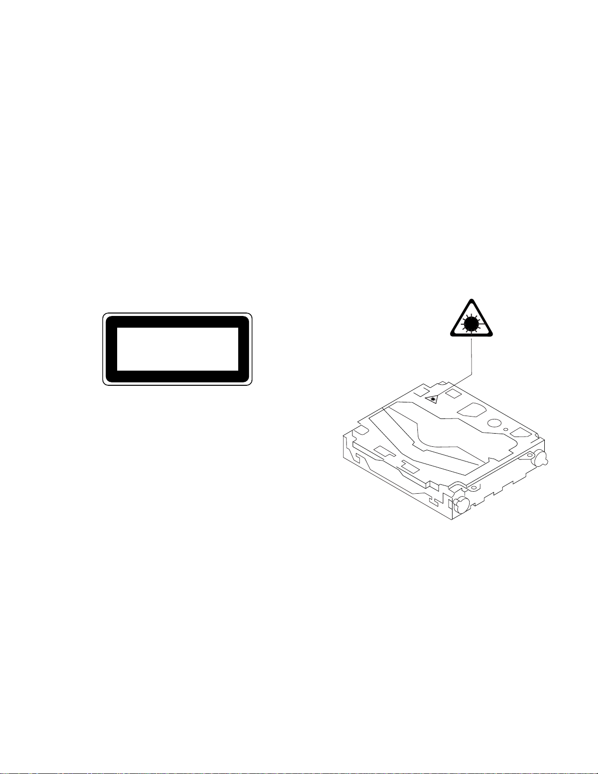
2. A “CLASS 1 LASER PRODUCT” label is affixed to the
rear of the player.
3. The triangular label is attached to the mechanism
unit frame.
4. Specifications of Laser Diode
Specifications of laser radiation fields to which human access is possible during service.
Wavelength = 800 nanometers
CLASS 1
LASER PRODUCT
Page 4
4
AVIC-505
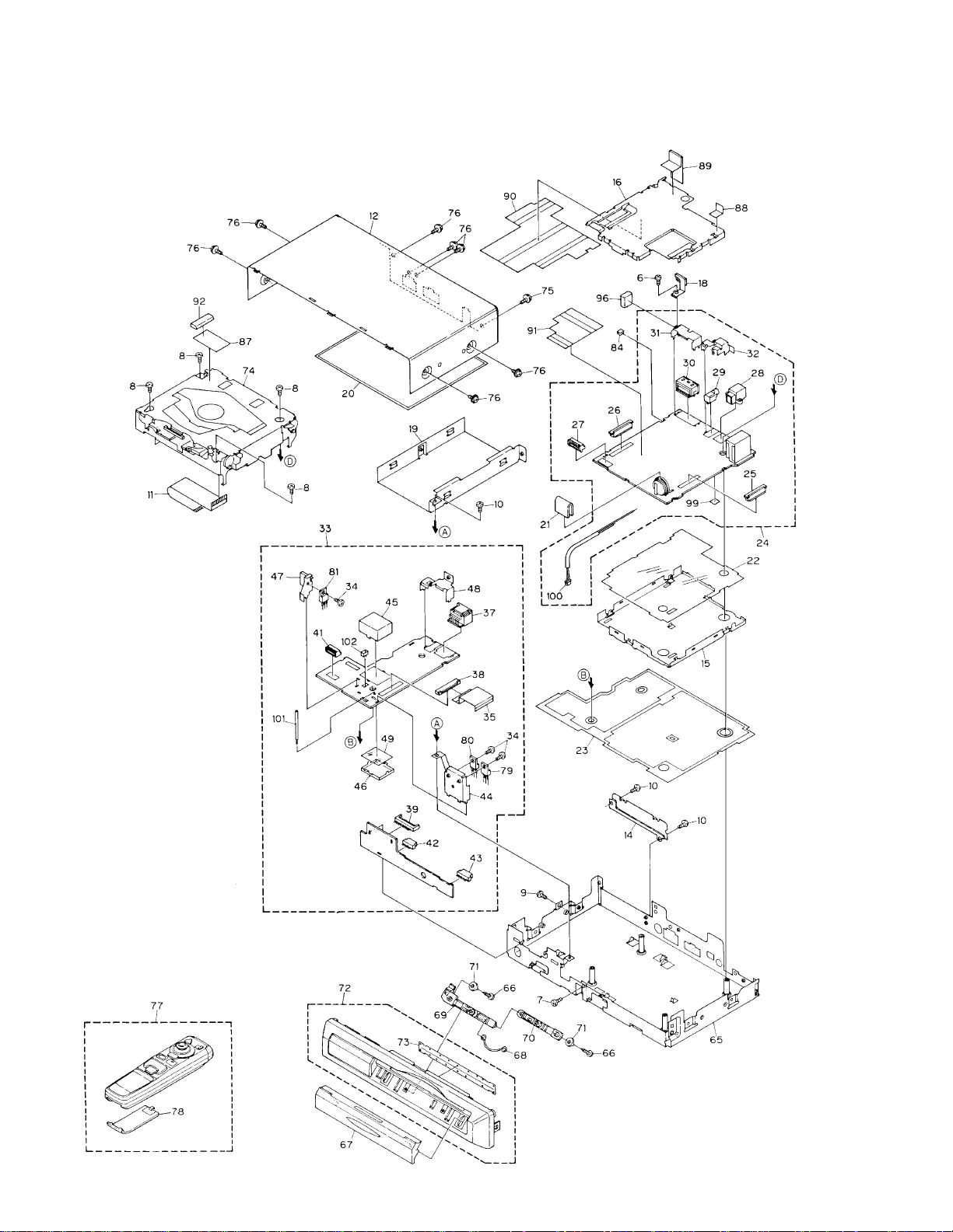
2. EXPLODED VIEWS AND PARTS LIST
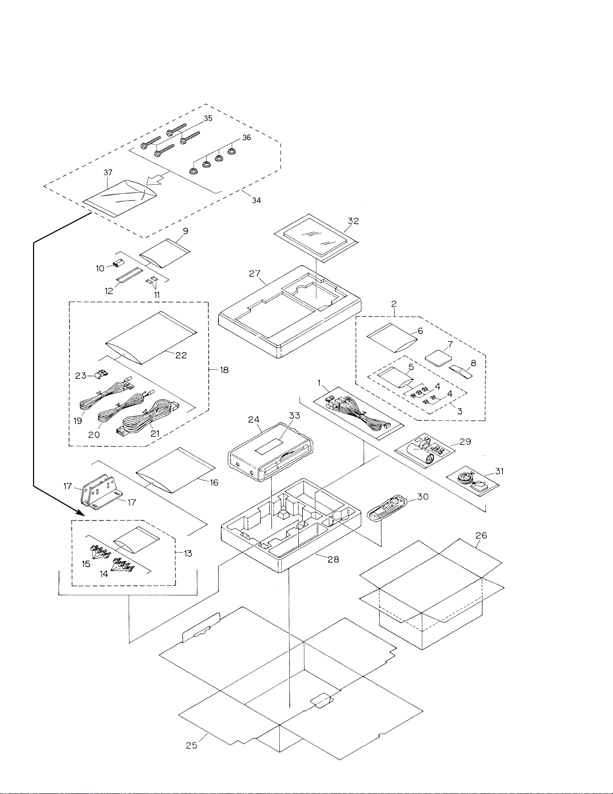
2.1 PACKING
Page 5
Part No.
Mark No. Symbol and Description AVIC-505/US AVIC-505/EW
18 Accessory Assy CEA2477 CEA2407
22 Polyethylene Bag CEG1182 * E36-609
24 Polyethylene Bag CEG1185 * CEG1088
25 Carton CHG3593 CHG3592
26 Contain Box CHL3593 CHL3592
* 32-1 Card ARY1048 Not used
32-2 Installation Manual CRB1422 CRD2635
32-3 Owner’s Manual CRB1520 Not used
* 32-5 Caution Card Not used ARY1048
* 33 Caution Card CRP1187 Not used
5
AVIC-505
(1) PACKING SECTION PARTS LIST
Mark No. Description Part No. Mark No. Description Part No.
NOTE:
- Parts marked by "*"are generally unavailable because they are not in our Master Spare Parts List.
- Screws adjacent to ∇ mark on the product are used for disassembly.
1 Cord Assy CDE5704
2 Accessory Assy CEA2228
3 Cord Clamp Assy CEA2072
4 Clamper CNV2581
* 5 Polyethylene Bag E36-615
6 Polyethylene Bag CEG1161
7 Sheet CNM4160
8 Water Proof Pad CNV2997
* 9 Polyethylene Bag CEG1101
10 Battery CEX1021
11 Fastener CNM4256
12 Fastener CNM4681
13 Screw Assy CEA2414
14 Screw(M6×16) CBA1295
15 Screw HMF50P080FZK
16 Polyethylene Bag CEG1022
17 Angle CNC5619
18 Accessory Assy
See Contrast table(2)
19 Cord CDE4685
20 Cord CDE5044
21 Cord Assy CDE5659
22 Polyethylene Bag
See Contrast table(2)
23 Connector CKX1049
24 Polyethylene Bag
See Contrast table(2)
25 Carton See Contrast table(2)
26 Contain Box See Contrast table(2)
27 Protector CHP2049
28 Protector CHP2050
29 Microphone Assy CPM1030
30 Remote Control Assy CXB2174
31 GPS Antenna Assy CXB2624
* 32-1 Card
See Contrast table(2)
32-2 Installation Manual See Contrast table(2)
32-3 Owner’s Manual See Contrast table(2)
* 32-4 Polyethylene Bag E36-634
* 32-5 Caution Card
See Contrast table(2)
* 32-6 Caution Card CRP1204
* 33 Caution Card
See Contrast table(2)
34 Screw Assy CEA2518
35 Screw HMB60P500FMC
36 Nut NF60FMC
* 37 Polyethylene Bag E36-615
- Owner’s Manual
Model Part No. Language
AVIC-505/US CRB1520 English
- Installation Manual
Model Part No. Language
AVIC-505/US CRB1422 English
AVIC-505/EW CRD2635 English, Spanish, German, French, Italian, Dutch
(2) CONTRAST TABLE
AVIC-505/US and AVIC-505/EW are constructed same except for the following:
Page 6
6
AVIC-505
2.2 EXTERIOR
Page 7
7
AVIC-505
Page 8

8
AVIC-505
1-5 •••••
6 Screw BMZ20P030FMC
7 Screw BMZ30P050FMC
8 Screw BSZ26P050FMC
9 Screw BSZ30P040FZK
10 Screw BSZ30P060FMC
11 FFC CDE5429
12 Case CNB2265
13 •••••
14 Cover CNB2314
15 Shield CNC7277
16 Shield CNC7939
17 •••••
18 Earth Terminal CNC7769
19 Rail CNC7893
20 Insulator CNM5396
21 Cushion CNM5591
22 Insulator CNM5884
23 Insulator CNM5776
24 Main Unit(AVIC-505/US) CWM5943
Main Unit(AVIC-505/EW) CWM5723
25 Connector(CN801) CKS2775
26 Connector(CN703) CKS2779
27 Connector(CN601) CKS2830
28 Socket(CN11) CKS3659
29 Jack(CN702) CKS3727
30 Connector(CN701) CKS3755
31 Holder CNC7274
32 Holder CNC7275
33 PS Unit CWM5729
34 Screw BMZ30P060FMC
35 FFC CDE5430
36 •••••
37 Connector(CN901) CKM1260
38 Connector(CN902) CKS1968
39 Connector(CN151) CKS2521
40 •••••
41 Connector(CN903) CKS2829
42 Connector(CN152) CKS3362
43 Connector(CN153) CKS3363
44 Holder CNC7272
45 Shield CNC7278
46 Shield CNC7279
47 Holder CNC7767
48 Holder CNC7770
49 Insulator CNM5777
50-64 •••••
65 Chassis Unit CXB2567
66 Screw BPZ20P080FMC
67 Door CAT1933
68 Spring CBH2106
69 Arm CNV5107
70 Arm CNV5108
71 Spacer CNV5109
72 Grille Unit CXB2114
73 Cover CNM4768
74 CD Mechanism Module CXK5052
75 Screw IMS30P060FZK
76 Screw ISS30P060FZK
77 Remote Control Assy CXB2174
78 Battery Cover CZN7543
79 Transistor(Q911) 2SB1566
80 IC(IC902) NJM78M08FA
81 Transistor(Q912) 2SD2396
82, 83 •••••
84 Spacer CNM5907
85, 86 •••••
87 Tape CNM5881
88 Tape CNM5882
89 Tape CNM5883
90 Insulator CNM5885
91 Insulator CNM5886
92 Cushion CNM5889
93-95 •••••
96 Cushion CNM5905
97, 98 •••••
99 Insulator CNM5780
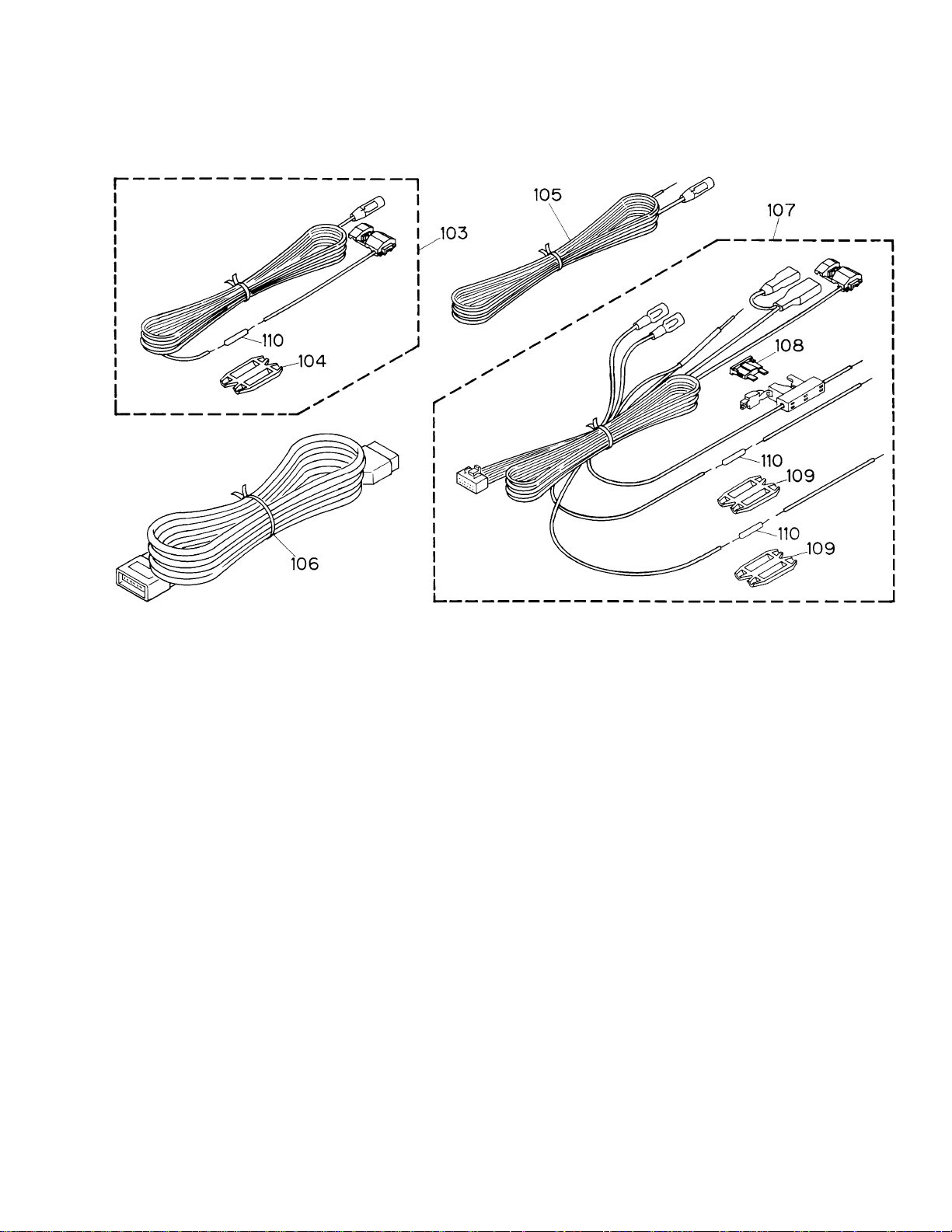
100 Cord CDE5731
101 Clamper(CN914) CEF1004
102 Connector(CN913) CKS2632
103 Cord CDE4685
104 Cap CNS1472
105 Cord CDE5044
106 Cord Assy CDE5659
107 Cord Assy CDE5704
108 Fuse CEK1135
109 Cap CNS1472
110 Resistor RS1/2PMF102J
- EXTERIOR SECTION PARTS LIST
Mark No. Description Part No. Mark No. Description Part No.
Page 9

9
AVIC-505
Page 10
10
AVIC-505
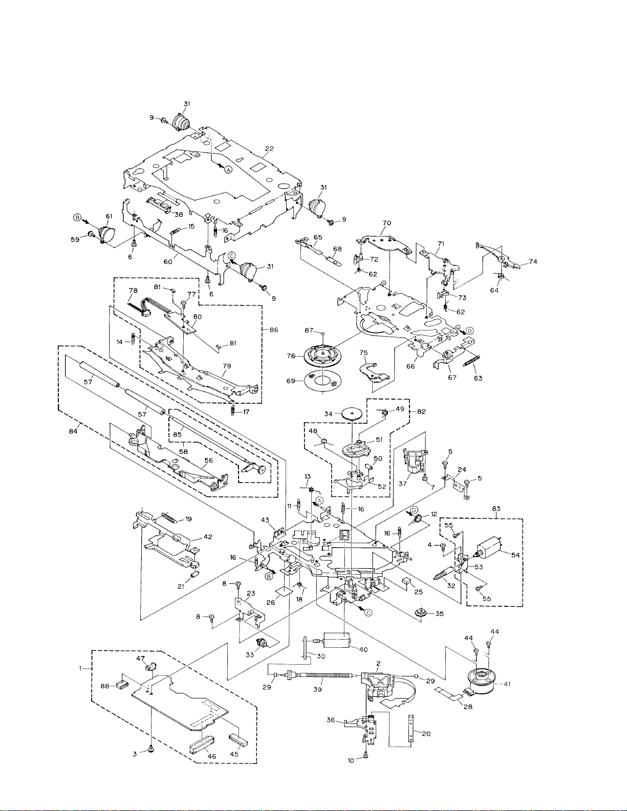
2.3 CD MECHANISM MODULE
Page 11

11
AVIC-505
1 Control Unit CWX2208
2 Pickup Unit(Service) CXX1230
3 Screw IMS26P035FMC
4 Screw BMZ20P025FMC
5 Screw BMZ20P040FMC
6 Screw BSZ20P040FMC
7 Screw(M2×3) CBA1077
8 Screw(M2×2) CBA1250
9 Screw(M2×5) CBA1296
10 Screw(M2×3.85) CBA1362
11 Spring CBH1724
12 Spring CBH1729
13 Spring CBH1730
14 Spring CBH1731
15 Spring CBH1732
16 Spring CBH1745
17 Spring CBH1848
18 Spring CBH1849
19 Spring CBH1939
20 Spring CBL1214
21 Roller CLA2627
22 Frame CNC5796
23 Bracket CNC5871
* 24 Bracket CNC6376
25 Cushion CNM3917
26 Sheet CNM4873
27 •••••
* 28 PCB CNP4288
29 Bearing CNR1415
30 Belt CNT1071
31 Damper CNV3974
32 Gear CNV4128
33 Gear CNV4129
34 Gear CNV4857
35 Gear CNV4131
36 Holder CNV4663
37 Holder CNV5071
38 Guide CNV4484
39 Screw Unit(S7) CXA8699
40 CRG Motor Unit(S7)(M2) CXB3043
41 Motor Unit(S7)(M1) CXB2199
42 Lever Unit CXA9300
43 Chassis Unit CXB2574
44 Screw JGZ17P025FZK
45 Connector(CN101) CKS1953
46 Connector(CN701) CKS2775
47 Connector(CN801) CKS2194
48 Spring CBH1832
49 Spring CBH1833
50 Roller CLA2627
51 Arm CNV4136
52 Arm Unit CXA8565
53 Bracket CNC6056
54 Load Motor Unit(S7)(M3) CXA8702
55 Screw JFZ20P025FMC
56 Arm CNV4120
57 Roller CNV4509
58 Gear Unit(S7) CXA8701
59 Screw(M2×5) CBA1455
60 Frame CNC5797
61 Damper CNV3974
62 Spring CBH1736
63 Spring CBH1863
64 Spring CBH1945
65 Spring CBL1269
66 Arm CNC5799
67 Lever CNC6054
68 Spacer CNM3315
69 Sheet CNM4981
70 Arm CNV5436
71 Arm CNV4123
72 Arm CNV4124
73 Arm CNV4125
74 Arm CNV4138
75 Arm CNV4139
76 Clamper CNV4737
77 Screw(M2×2) CBA1250
* 78 Connector(CN1) CDE5000
79 Arm CNC7383
* 80 Gathering PCB CNX2445
81 Photo-transistor(Q1, 2) CPT-230S-X
82 ELBO Arm Assy(S7) CXA8889
83 Load Motor Assy(S7) CXA8891
84 LO Arm Assy(S7) CXA8892
85 Shaft CLA3133
86 Guide Arm Assy(S7) CXA9158
87 Ball CNR1189
88 Connector(CN802) CKS1944
- CD MECHANISM MODULE SECTION PARTS LIST
Mark No. Description Part No. Mark No. Description Part No.
Page 12
12
AVIC-505
1
23
4
1
234
D
C
B
A
C
B
GUIDE ON
CORD ASSY
PS PCB
GRILLE PCB
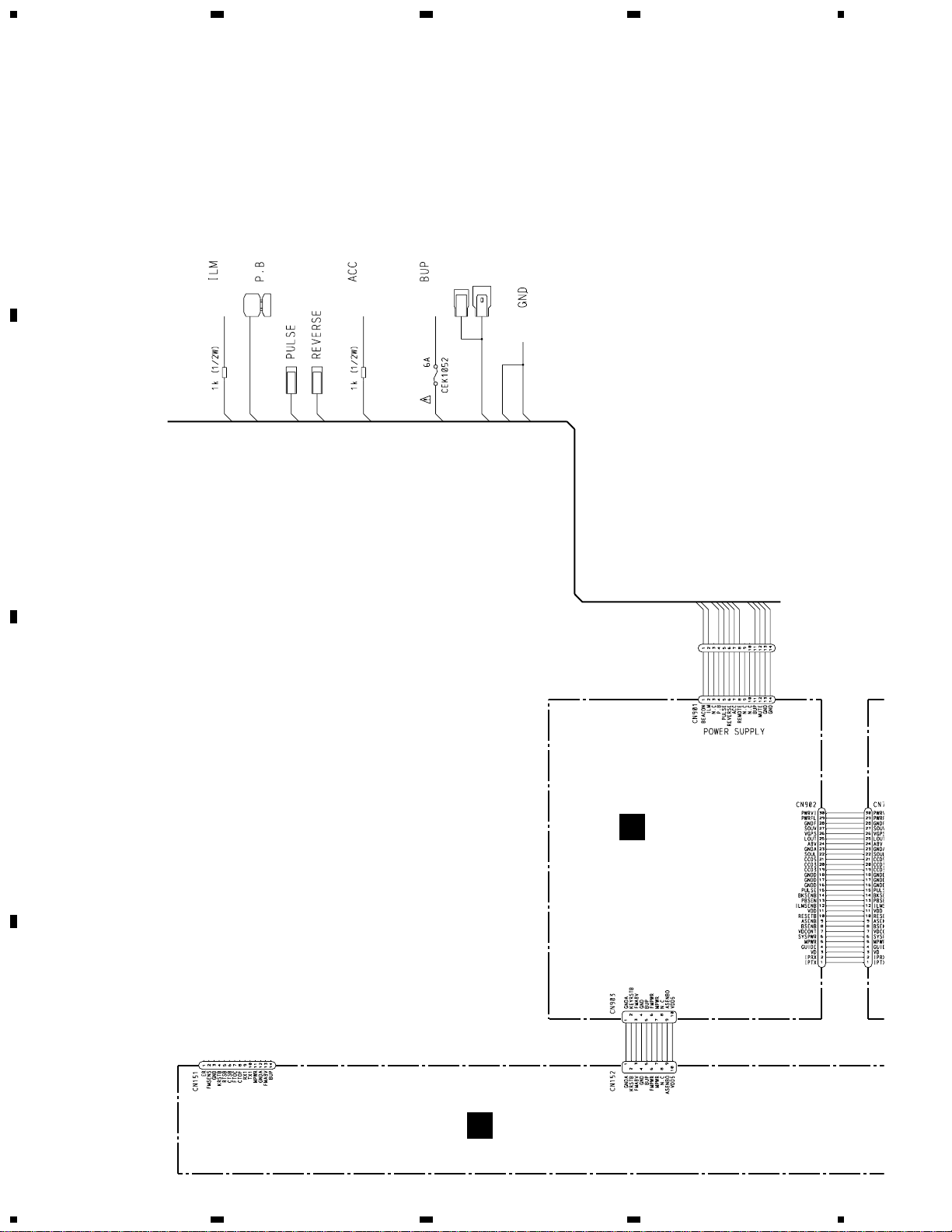
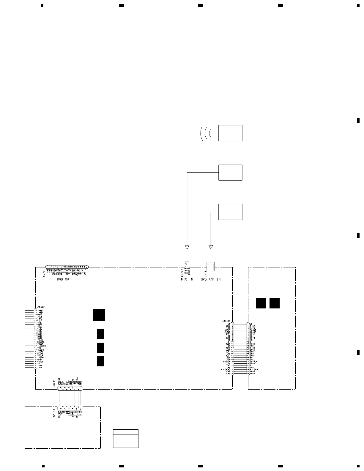
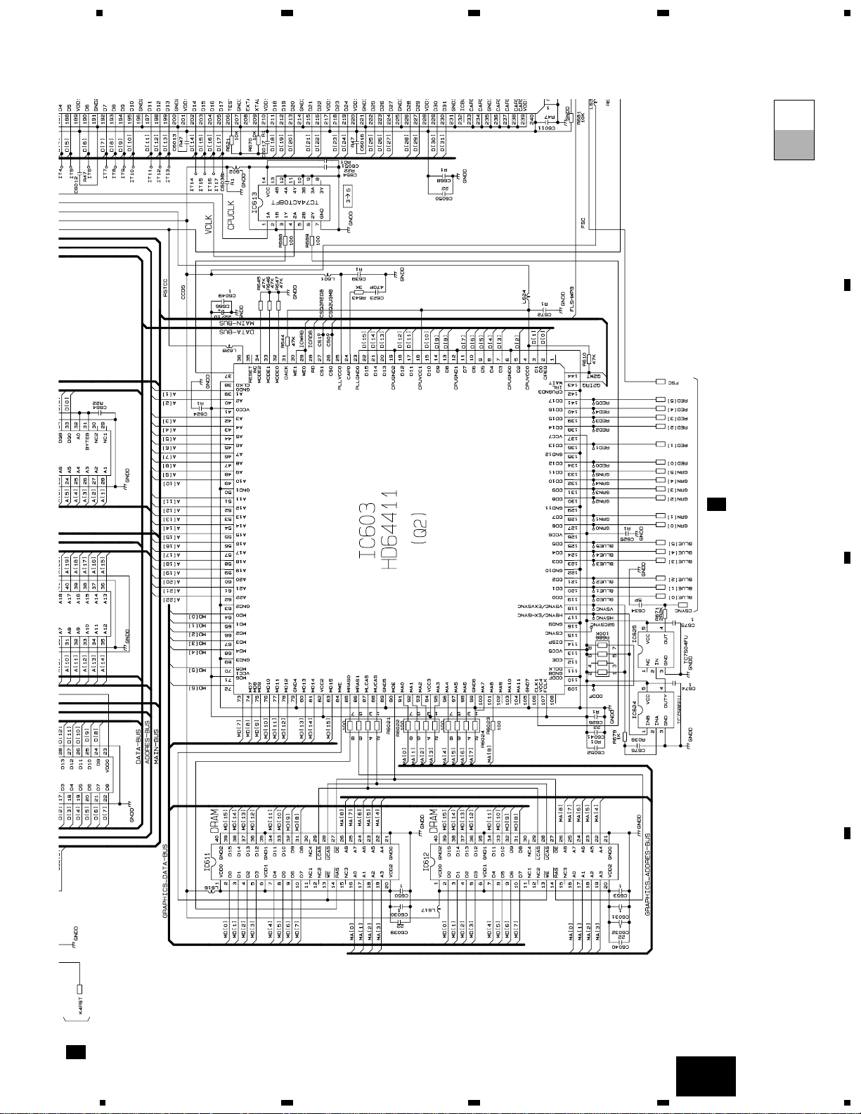
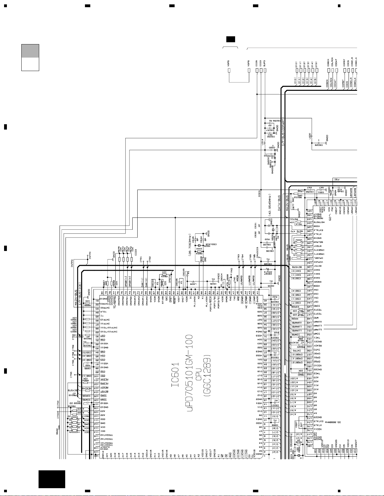
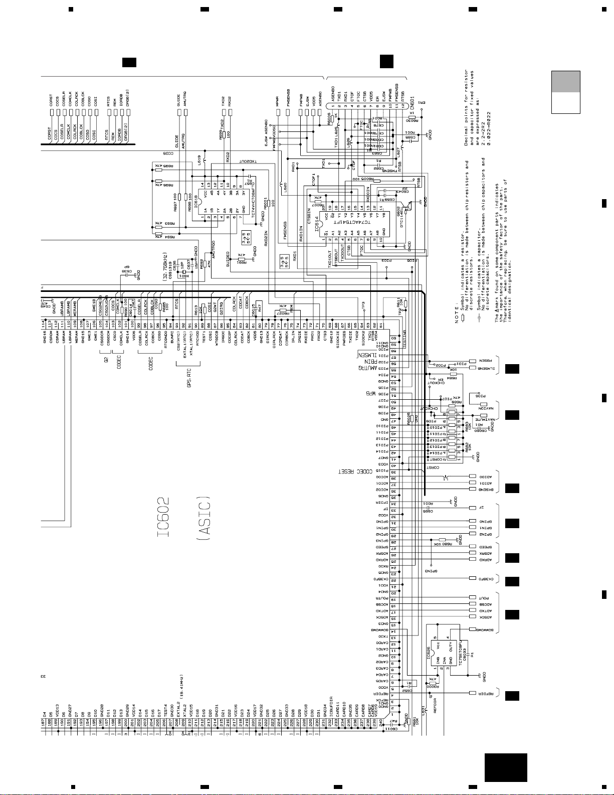
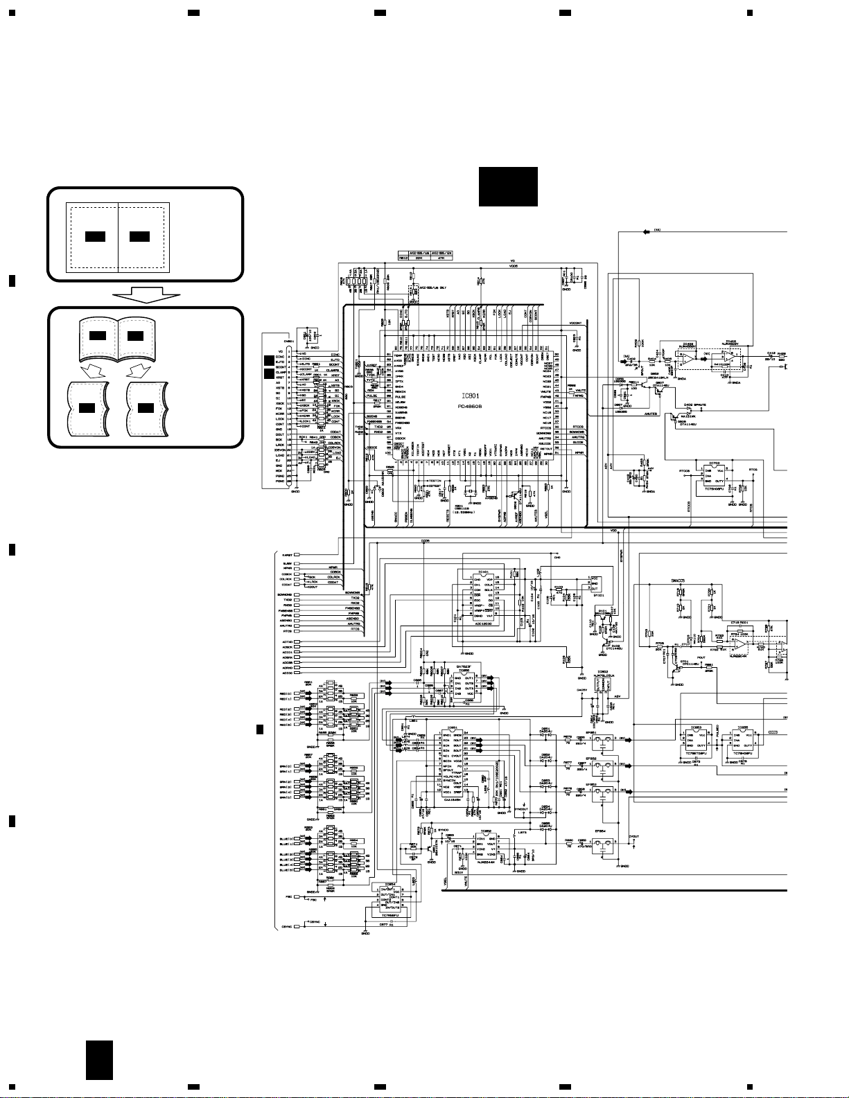
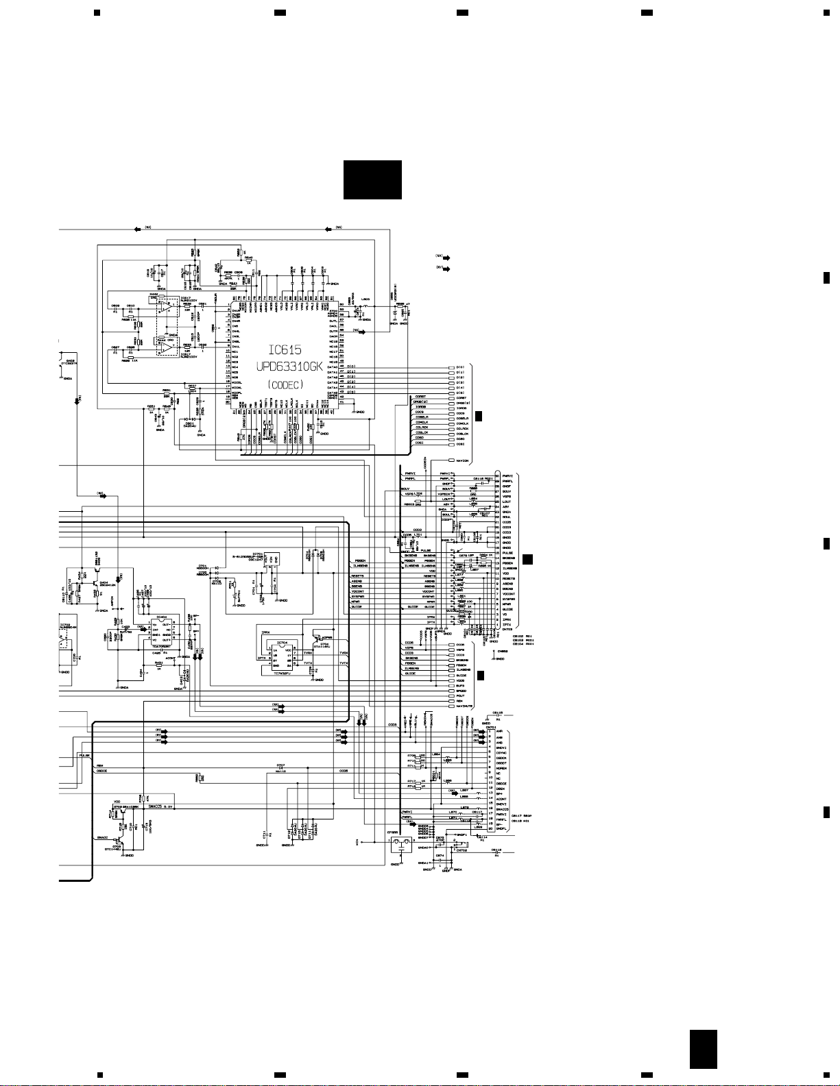
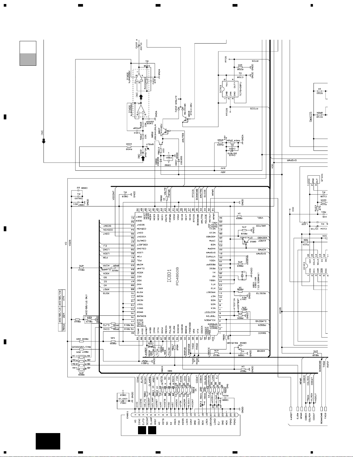
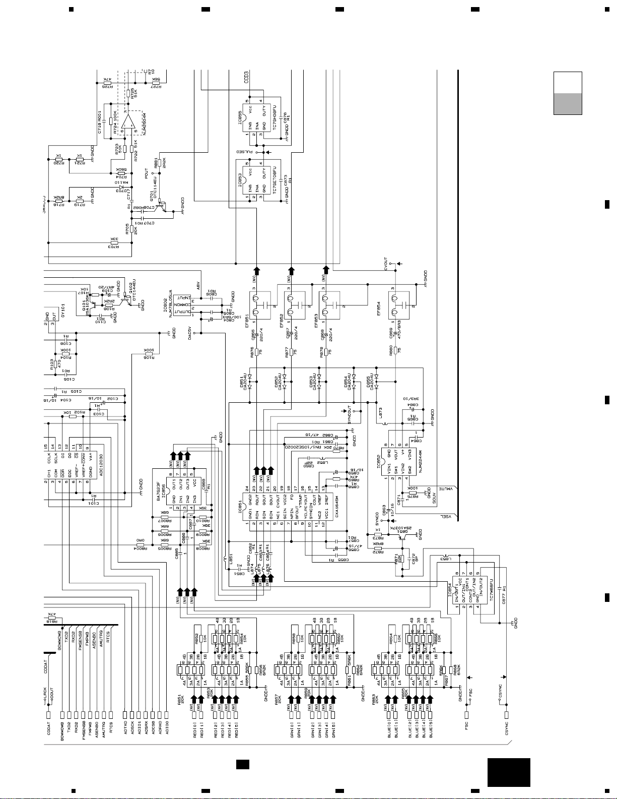
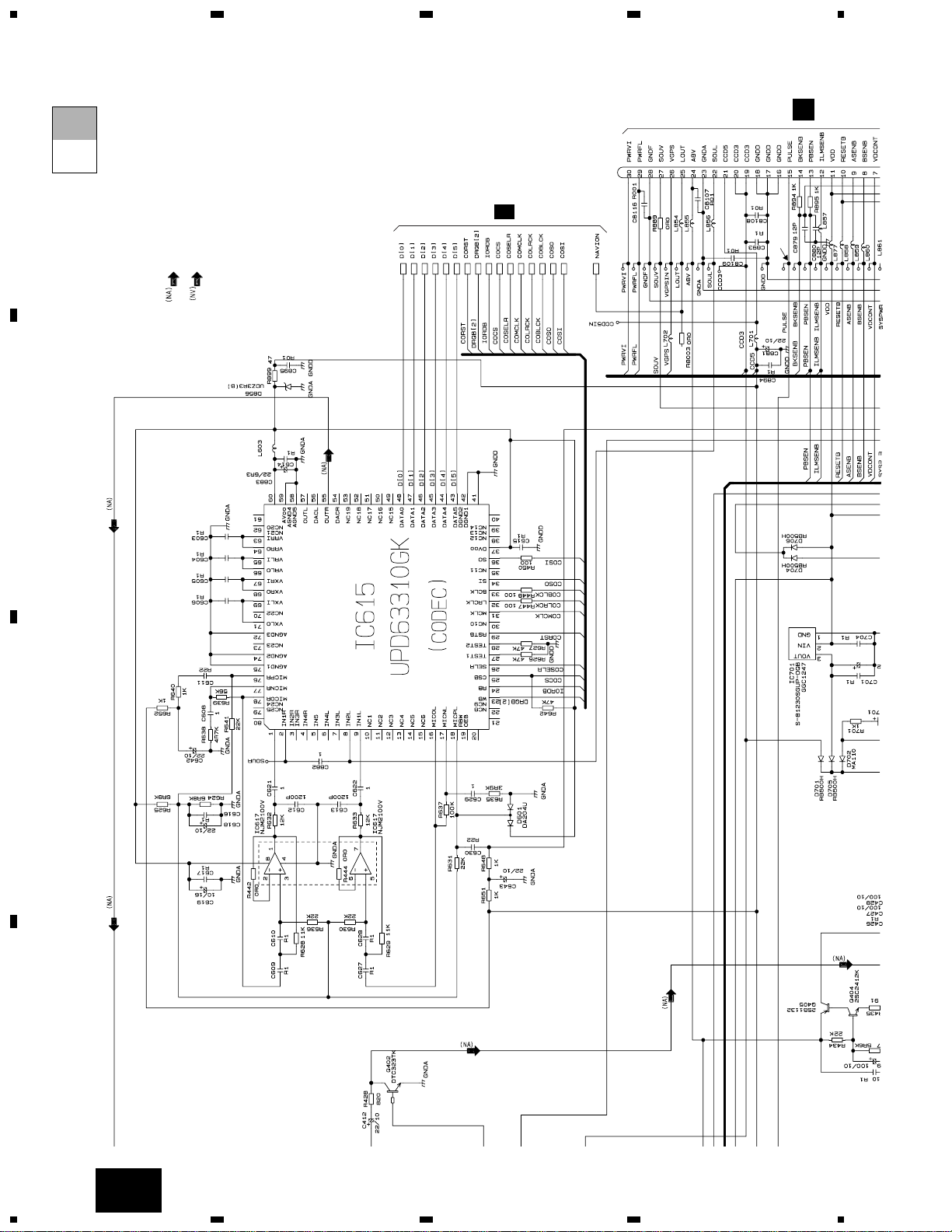
3. SCHEMATIC DIAGRAM
3.1 OVERALL CONNECTION DIAGRAM
Note: When ordering service parts, be sure to refer to “EXPLODED VIEWS AND PARTS LIST” or “ELECTRICAL
PARTS LIST”.
Page 13
13
AVIC-505
5
6
78
5
6
78
D
C
B
A
A
1/3
A
2/3
A
3/3
D E
PS UNIT
Consists of
Grille PCB
PS PCB
MAIN UNIT
GPS ANTENNA ASSY
MICROPHONE ASSY
REMOTE CONTROL ASSY
CD MECHANISM
MODULE
CC SECTION
IF SECTION
GPS SECTION
A
Page 14
AVIC-505
1
23
4
1
234
D
C
B
A
M5M4V17805DTP-6S
TC51V17805CFTS-60
(GGC1293)
TC51V17805CFTS-60
(GGC1293)
LH28F032SUHTD-70(GGC1290)
PD8052B
M5M51016BTP-10VH (GGC1295)
MSM514265C-60TS
MSM514265C-60TS
A
2/3
A
2/3
MAIN DRAM × 4
CAR CONTROL
RESET CIRCUIT
MAIN MEMORY
SRAM
MAIN MEMORY ROM
GRAPHICS PROCESSING MEMORY
DRAM × 2
GRAPHICS PROCESSING
(GRAPHICS RENDELER)
CPUCLK
VCLK
LEVEL
CONVERTER
M5M4V17805DTP-6S
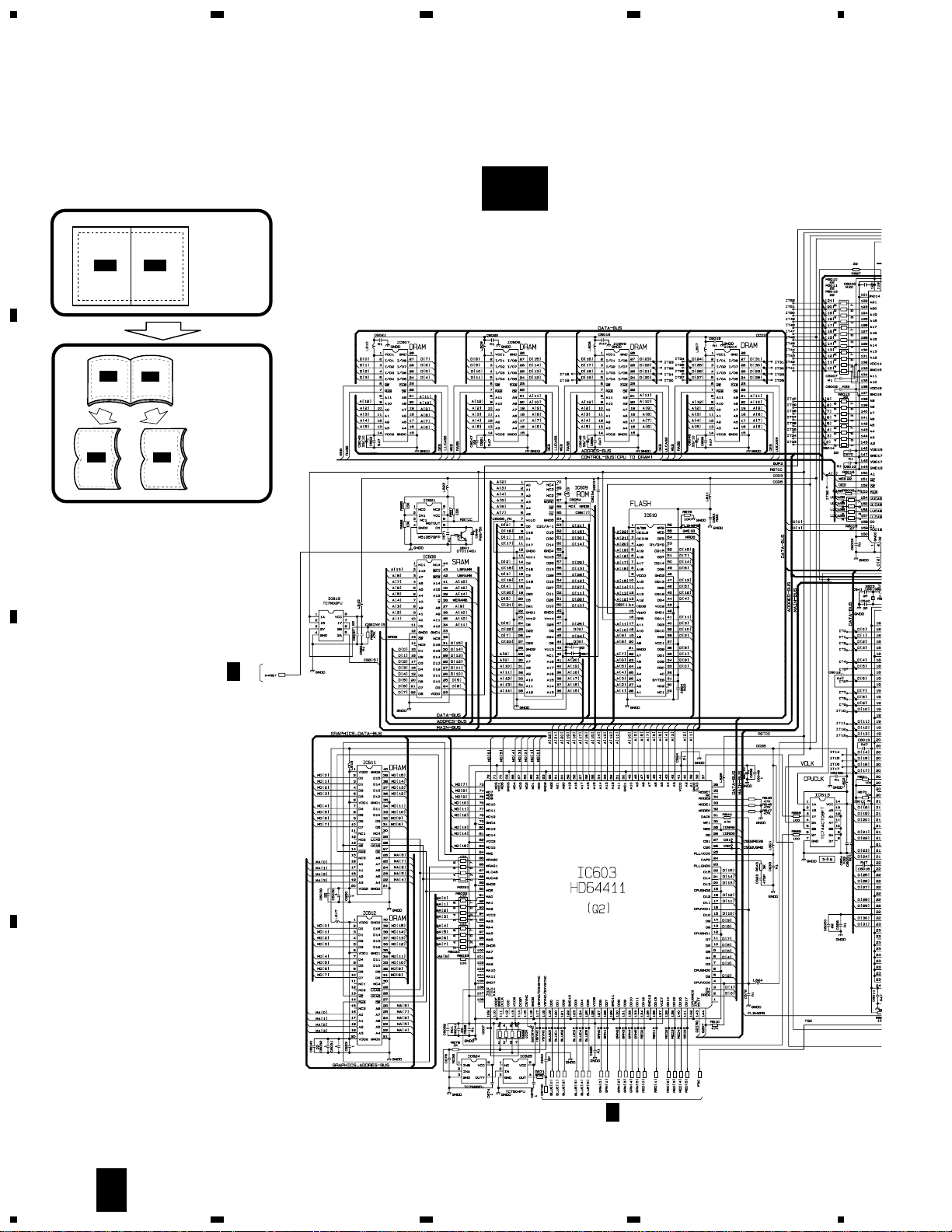
3.2 MAIN UNIT(1/3)(GUIDE PAGE)
- CC SECTION
A-a A-b
A-aA-a
A-b A-b
A-b A-b
A-a A-a
Large size
SCH diagram
Guide page
Detailed page
A-a
14
A
1/3
Page 15
15
AVIC-505
5
6
78
5
6
78
D
C
B
A
PD4844B
(GGC1296)
A
3/3
A
2/3
B
CN153
A
2/3A2/3
A
2/3
A
2/3
A
2/3A3/3
A
3/3
A
3/3
MAIN CPU
GPS, GYRO SIGNAL PROCESSING,
RTC, CODEC I/F,
PSG, PERIPHERAL ASIC
CAR CONTROL TO MULTI-FM, EXTERNAL
COMMIUNICATION GATE
CAR CONTROL TO
SYSTEM µ-COM
COMMUNICATION GATE
GUIDE OUTPUT
ASEN INPUT
MODEM CONTROL
TEST MODE
A-b
A
1/3
Page 16
16
AVIC-505
1
23
4
1
234
D
C
B
A
M5M4V17805DTP-6S
TC51V17805CFTS-60
(GGC1293)
TC51V17805CFTS-60
(GGC1293)
M5M4V17805DTP-6S
LH28F032SUHTD-70(GGC1290)
PD8052B
M5M51016BTP-10VH (GGC1295)
A
2/3
MAIN DRAM × 4
CAR CONTROL
RESET CIRCUIT
A-a
A-b
1/3
A-a
Page 17
17
AVIC-505
5
6
78
5
6
78
D
C
B
A
M5M5101
MSM514265C-60TS
MSM514265C-60TS
A
2/3
A
2/3
MAIN MEMORY
SRAM
MAIN MEMORY ROM
GRAPHICS PROCESSING MEMORY
DRAM × 2
GRAPHICS PROCESSING
(GRAPHICS RENDELER)
CPUCLK
VCLK
LEVEL
CONVERTER
A-a
A-b
1/3
A-a
Page 18
18
AVIC-505
1
23
4
1
234
D
C
B
A
A-a
A-b
A
3/3
MAIN CPU
1/3
A-b
Page 19
19
AVIC-505
5
6
78
5
6
78
D
C
B
A
A-a
A-b
PD4844B
(GGC1296)
A
2/3
B
CN153
A
2/3
A
2/3
A
2/3
A
2/3
A
2/3
A
3/3
A
3/3
A
3/3
GPS, GYRO SIGNAL PROCESSING,
RTC, CODEC I/F,
PSG, PERIPHERAL ASIC
CAR CONTROL TO MULTI-FM, EXTERNAL
COMMIUNICATION GATE
CAR CONTROL TO
SYSTEM µ-COM
COMMUNICATION GATE
GUIDE OUTPUT
ASEN INPUT
MODEM CONTROL
TEST MODE
1/3
A-b
Page 20
20
AVIC-505
1
23
4
1
234
D
C
B
A
3.3 MAIN UNIT(2/3)(GUIDE PAGE)
- IF SECTION
VIDEO D/A
GYRO D/A
GYRO
RGB BUFFER
NTSC ENCODER
VIDEO
POWER SUPPLY
CSYNC / TV VIDEO SELECT SW AND 75Ω DRIVER
COMPLEMENT OF
CAR SPEED PULSE
WAVEFORM
POWER
POWER S
SP OUTPUT
MU
LPF
AMUTE DRIVER
A
1/3
#
&
@
2
3!
*
SYSTEM CD CONTROL µ-COM
CD MECHANISM MODULE
ED
0
A-a A-b
A-aA-a
A-b A-b
A-b A-b
A-a A-a
Large size
SCH diagram
Guide page
Detailed page
A-a
A
2/3
Page 21
21
AVIC-505
5
6
78
5
6
78
D
C
B
A
POWER AMP
+ VCA
SRAM, RTC
POWER SUPPLY
SYSTEM µ-COM to
TV µ-COM COMMUNICATION GATE
AUDIO MICROPHONE INPUT
CODEC POWER SUPPLY
NOISE INPUT
HPF(NOISE)
HPF(AUDIO)
AUDIO INPUT
A
1/3
CN902
C
: NAVI AUDIO SIGNAL
: NAVI VIDEO SIGNAL
A
1/3
MONITOR
$
7
8
9
(
RECEIVING PART
PULSE CIRCUIT
POWER SUPPLY
RGB HOLDER
RGB HOLDER
RGB HOLDER
CKS2310(BLACK)
CKS3727(RED)
CKS3727(BLACK)
EXAMINATION
CONNECTOR
^
A-b
A
2/3
Page 22
22
AVIC-505
1
23
4
1
234
D
C
B
A
GYRO D/A
GYRO
COMPLEMENT OF
CAR SPEED PULSE
WAVEFORM
POW
POWE
SP OUT
LPF
AMUTE DRIVER
*
SYSTEM CD CONTROL µ-COM
CD MECHANISM MODULE
ED
A-a
A-b
2/3
A-a
Page 23
23
AVIC-505
5
6
78
5
6
78
D
C
B
A
@
VIDEO D/A
RGB BUFFER
NTSC ENCODER
VIDEO
POWER SUPPLY
CSYNC / TV VIDEO SELECT SW AND 75Ω DRIVER
A
1/3
#
&
2
3!
0
A-a
A-b
2/3
A-a
Page 24
1
24
AVIC-505
1
23
4
234
D
C
B
A
A-a
A-b
POWER AMP
POWER SUPPLY
SRAM, RTC
POWER SUPPLY
CODEC POWER SUPPLY
NOISE INPUT
HPF(NOISE)
HPF(AUDIO)
AUDIO INPUT
MUTE
A
1/3
CN902
C
: NAVI AUDIO SIGNAL
: NAVI VIDEO SIGNAL
^
2/3
A-b
Page 25
25
AVIC-505
5
6
78
5
6
78
D
C
B
A
A-a
A-b
POWER AMP
+ VCA
SYSTEM µ-COM to
TV µ-COM COMMUNICATION GATE
AUDIO MICROPHONE INPUT
A
1/3
MONITOR
$
7
8
9
(
RECEIVING PART
PULSE CIRCUIT
POWER SUPPLY
RGB HOLDER
RGB HOLDER
RGB HOLDER
CKS2310(BLACK)
CKS3727(RED)
CKS3727(BLACK)
EXAMINATION
CONNECTOR
2/3
A-b
Page 26
26
AVIC-505
1
23
4
1
234
D
C
B
A
3.4 MAIN UNIT(3/3)
- GPS SECTION
GPS.
ANT IN
A
1/3
CCH1294
A
3/3
Page 27
27
AVIC-505
1
2
34
1
2
3
D
C
B
A
B
PS UNIT
Consists of
Grille PCB
PS PCB
GRILLE PCB
C
CN903
A
CN601
3.5 GRILLE PCB
4
B
Page 28
C
PS PCB
PS UNIT
Consists of
Grille PCB
PS PCB
B
CN152
A
CN703
8.5V REGULATOR
8V REGULATOR
9V REGULATOR
LAMP RECEIVING PART
ILLUMINATION
BACK LIGHT
POWER SUPPLY
3.3V
REGULATOR
5V
1
28
AVIC-505
1
23
4
1
234
D
C
B
A
3.6 PS PCB
C
Page 29
CORD ASSY
5V DC/DC CONVERTER
ACC / B.UP SENSE, RESET,
B.UP LINKAGE, VDD5V POWER SUPPLY
ILLUMINATION SENSE
PARKING SENSE
MUTE
BACK SENSE
PULSE IN
MONITOR CONTROL
OUTPUT
1
%
29
AVIC-505
5
6
78
5
6
7
D
C
B
A
8
C
Page 30
30
AVIC-505
- Waveforms
2 MAIN UNIT TP FSC 500mV/div. 200ns/div.
3 MAIN UNIT TP CSYNC 2V/div. 20µs/div.
7 MAIN UNIT TP RED
8 MAIN UNIT TP GRE
9 MAIN UNIT TP BLU 1V/div. 10µs/div.
0 MAIN UNIT TP SYNCOUT
At test disc color bar indication
1 PS PCB TP FREQ3 5V/div. 2µs/div.
Note:The numbers circled are the measure points of the circuit
diagram of page 20 to 29.
8
7
9
0
3
1
2
Page 31

31
AVIC-505
! MAIN UNIT TP CSYNC 5V/div.
@ MAIN UNIT TP SYNC0 2V/div. 50µs/div.
# MAIN UNIT TP CVOUT 500mV/div.
At test disc color bar indication
$ MAIN UNIT TP REMIN 1V/div. 5ms/div.
At remote control sending
% PS PCB TP PULSE1 5V/div.
^ MAIN UNIT TP PULSE 2V/div. 200µs/div.
& MAIN UNIT TP PULSE0 5V/div.
At inputting 5Vp-p,1kHz square wave to the power
supply cord "CAR SPEED SIGNAL INPUT"
* MAIN UNIT TP SPOUT 1V/div.
( MAIN UNIT TP AMPIN 1V/div. 200µs/div.
At test disc 11kHz sampling 1kHz sine wave
regeneration
!
@
%
^
&
*
(
$
#
Page 32

32
AVIC-505
1
23
4
1
234
D
C
B
A
3.7 CD MECHANISM MODULE(GUIDE PAGE)
A-a A-b
A-aA-a
A-b A-b
A-b A-b
A-a A-a
Large size
SCH diagram
Guide page
Detailed page
E
D
CXB3043
CXB2199
CXA8702
D
E
D-a
Page 33

8
33
AVIC-505
5
6
78
5
6
7
D
C
B
A
A
D
D-b
Page 34

AVIC-505
1
23
4
1
234
D
C
B
A
D-a
D-b
D
34
D-a
Page 35

35
AVIC-505
5
6
78
5
6
78
D
C
B
A
D-a
D-b
E
CXB3043
CXB2199
CXA8702
E
D-a
Page 36

36
AVIC-505
1
23
4
1
234
D
C
B
A
D-a
D-b
D-b
Page 37

37
AVIC-505
5
6
78
5
6
78
D
C
B
A
D-a
D-b
A
D-b
Page 38

38
AVIC-505
- Waveforms
1 RFO 0.5V/div. 0.5µs/div.
Normal mode: play
1 CH1: RFO 1V/div.
2 CH2: MIRR 5V/div.
Test mode: Tracking open
0.5ms/div.
1 CH1: RFO 1V/div.
2 CH2: MIRR 5V/div.
Normal mode:The defect part passes
800µm
0.5ms/div.
3 CH1: FIN 0.5V/div.
4 CH2: FO+ 2V/div.
Test mode: No disc, Focus close
0.2s/div.
3 CH1: FIN 0.5V/div.
5 CH2: FOK 2V/div.
Normal mode: Focus close
0.2s/div.
6 CH1: FEY 0.5V/div.
7 CH2: XSI 2V/div.
Normal mode: Focus close
1ms/div.
REFO
→
8 CH1: TEY 0.5V/div.
9 CH2: TIN 0.5V/div.
Test mode: 32 tracks jump (FWD)
0.5ms/div.
8 CH1: TEY 0.5V/div.
9 CH2: TIN 0.5V/div.
Test mode: Single jump (FWD)
0.5ms/div.
8 CH1: TEY 0.5V/div.
9 CH2: TIN 0.5V/div.
Test mode: 100 tracks jump (FWD)
5ms/div.
6 CH1: FEY 0.1V/div.
3 CH2: FIN 0.2V/div.
Normal mode: Play
20ms/div.
3 CH1: FIN 0.5V/div.
0 CH2: EC 1V/div.
Normal mode: Focus close (12cm)
0.2s/div.
3 CH1: FIN 0.5V/div.
0 CH2: EC 1V/div.
Normal mode: Focus close (8cm)
0.2s/div.
GND
→
GND
→
REFO
→
REFO
→
REFO
→
REFO
→
GND
→
REFO
→
REFO
→
GND
→
REFO
→
REFO
→
REFO
→
REFO
→
REFO
→
REFO
→
REFO
→
REFO
→
REFO
→
REFO
→
REFO
→
REFO
→
Note:1. The numbers circled are measure points of the circuit diagram of page 32 to37
2. Reference voltage
REFO:2.5V
Page 39

39
AVIC-505
8 CH1: TEY 0.2V/div.
9 CH2: TIN 0.2V/div.
Normal mode: play
8 CH1: TEY 0.5V/div.
! CH2: SD 0.5V/div.
5ms/div.
0 EC 0.5V/div. 0.1s/div.
Normal mode : Audio disc long search
(12cm)
@ EFM 1V/div. 5µs/div.
Play
8 CH1: TEY 1V/div.
# CH2: TEC 1V/div.
Test mode: Focus close
Tracking open
2ms/div.
8 CH1: TEY 0.5V/div.
6 CH2: FEY 0.5V/div.
Normal mode: AGC after focus
close
0.2s/div.
$ PLCK 2V/div. 0.5µs/div.
Play
20ms/div.
% SCKO 2V/div. 1µs/div.
Play
^ Dout 2V/div. 10µs/div.
Play
& LRCK 2V/div. 20µs/div. * VD 5V/div. 50ms/div.
Normal mode: No disc
REFO
→
REFO
→
GND
→
REFO
→
REFO
→
REFO
→
REFO
→
REFO
→
REFO
→
REFO
→
GND
→
REFO
→
GND
→
REFO
→
GND
→
REFO
→
GND
→
REFO
→
REFO
→
REFO
→
Page 40

40
AVIC-505
6 CH1: FEY 0.2V/div.
3 CH2: FIN 0.5V/div.
Normal mode: During AGC
1ms/div.
8 CH1: TEY 0.2V/div.
9 CH2: TIN 0.5V/div.
Normal mode: During AGC
1 CH1: RFO 1V/div.
⁄ CH2: HOLD 5V/div.
Normal mode: The defect part passes
800µm
1ms/div.
0.5ms/div.
3 CH1: FIN 1V/div.
⁄ CH2: HOLD 5V/div.
Normal mode: The defect part passes
800µm
0.5ms/div.
GND
→
GND
→
REFO
→
REFO
→
REFO
→
REFO
→
0 CH1 : EC 0.5V/div.
¤ CH2 : SCONT 2V/div.
Normal mode: During play audio disc
(Spindle normal speed)
0 CH1 : EC 0.5V/div.
¤ CH2 : SCONT 2V/div.
Normal mode: During play map disc
(Spindle double speed)
0.1s/div.
0.1s/div.
REFO
→
REFO
→
REFO
→
REFO
→
Page 41

41
AVIC-505
Page 42

42
AVIC-505
1
23
4
234
D
C
B
A
MAIN UNIT
1
4. PCB CONNECTION DIAGRAM
4.1 MAIN UNIT
A
A
B
CN153
C
CN902
E
CN701
Page 43

43
AVIC-505
5
6
78
5
6
78
D
C
B
A
Capacitor
Connector
P.C.Board
Chip Part
SIDE A
SIDE B
NOTE FOR PCB DIAGRAMS
1. The parts mounted on this PCB include all necessary
parts for several destination.
For further information for respective destinations,
be sure to check with the schematic diagram.
2. Viewpoint of PCB diagrams
A
SIDE A
RGB OUT
Page 44

44
AVIC-505
1
23
4
1
234
D
C
B
A
MAIN UNIT
A
A
Page 45

45
AVIC-505
5
6
78
5
6
7
8
D
C
B
A
SIDE B
A
Page 46

46
AVIC-505
1
23
4
1
234
D
C
B
A
GRILLE PCB
4.2 GRILLE PCB
SIDE A
B
B
C
CN903
A
CN601
EJECT
Page 47

47
AVIC-505
1
2
34
1
2
34
D
C
B
A
SIDE B
GRILLE PCB
B
B
RESET
Page 48

48
AVIC-505
1
23
4
1
234
D
C
B
A
4.3 PS PCB
PS PCB
SIDE A
C
C
CORD
ASSY
A
CN703
B
CN152
Page 49

49
AVIC-505
1
2
34
1
2
34
D
C
B
A
SIDE B
PS PCB
C
C
Page 50

50
AVIC-505
1
23
4
1
234
D
C
B
A
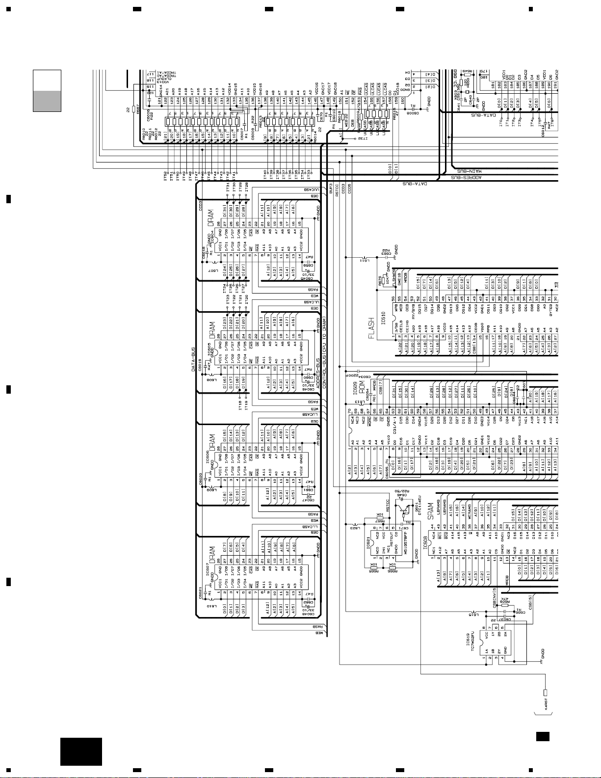
4.4 CD MECHANISM MODULE
F
E
REFO
CN801
SERVICE
PICKUP UNIT
M1
SPINDLE
CN801
CONTROL UNIT
SIDE A
D
E
D
PHOTO UNIT
E
D
A
Page 51

51
AVIC-505
1
2
34
1
2
34
D
C
B
A
SIDE B
D
CONTROL UNIT
D
E
HOME
CLAMP
Page 52

52
AVIC-505
5. ELECTRICAL PARTS LIST
NOTES:
- Parts whose parts numbers are omitted are subject to being not supplied.
- The part numbers shown below indicate chip components.
Chip Resistor
RS1/_S___J,RS1/__S___J
Chip Capacitor (except for CQS.....)
CKS....., CCS....., CSZS.....
=====Circuit Symbol and No.===Part Name Part No.
--- ------ ------------------------------------------ -------------------------
Unit Number : CWM5943(AVIC-505/US)
Unit Number : CWM5723(AVIC-505/EW)
Unit Name : Main Unit
MISCELLANEOUS
IC 11 IC PM6003A
IC 71 IC TC7SU04F
IC 81 IC NJM2904M
IC 101 IC ADC12030
IC 402 IC NJM4558V
IC 404 IC TDA7052BT
IC 601 IC (UPD705101GM-100) GGC1289
IC 602 IC PD4844B
IC 603 IC HD64411
IC 604 IC M5M4V17805DTP-6S
IC 605 IC (TC51V17805CFTS-60) GGC1293
IC 606 IC (TC51V17805CFTS-60) GGC1293
IC 607 IC M5M4V17805DTP-6S
IC 608 IC (M5M51016BTP-10VH) GGC1295
IC 609 IC PD8052B
IC 610 IC (LH28F032SUHTD-70) GGC1290
IC 611 IC MSM514265C-60TS
IC 612 IC MSM514265C-60TS
IC 613 IC TC74ACT08FT
IC 614 IC TC74ACT541FT
IC 615 IC UPD63310GK
IC 617 IC NJM2100V
IC 618 IC (TC74VHCT08AFT) GGC1296
IC 619 IC TC7W02FU
IC 621 IC M51957BFP
IC 624 IC TC7S86FU
IC 625 IC TC7S04FU
IC 626 IC TC7SET08FU
IC 701 IC (S-81230SGUP-DQB) GGC1247
IC 702 IC NJM2904M
IC 703 IC TC7SH08FU
IC 704 IC TC7W32FU
IC 801 IC PD4860B
IC 802 IC NJM78L05UA
IC 851 IC CXA1645M
IC 852 IC NJM2244M
IC 853 IC TC7SET08FU
IC 854 IC TC7W66FU
IC 855 IC TC7SH08FU
IC 856 IC BA7623F
Q 11 Micro Transistor 2SC5081
Q 81 Transistor 2SB1132
Q 101 Transistor 2SA1036K
Q 102 Transistor DTC144EU
Q 402 Transistor DTC323TK
Q 404 Transistor 2SC2412K
Q 405 Transistor 2SB1132
Q 601 Transistor DTC114EU
Q 602 Transistor DTC114EU
Q 701 Transistor DTC114EU
Q 702 Transistor 2SA1036K
Q 703 Transistor DTC144EU
Q 704 Transistor DTA114EU
Q 802 Transistor DTA114EU
Q 807 Transistor DTA114EU
Q 808 Transistor DTA114EU
Q 851 Transistor 2SA1037K
Q 852 Transistor 2SC2412KLN
D 31 Diode HVU355
D 402 Chip Diode MA151WK
D 403 Diode Network DA204U
D 601 Diode Network DA204U
D 701 Diode RB500H
D 702 Diode MA110
D 703 Diode MA110
D 704 Diode RB500H
D 705 Diode RB500H
D 706 Diode RB500H
D 707 Diode MA110
D 711 Diode Network DA204U
D 712 Diode Network DA204U
D 715 Diode Network DA204U
D 802 Chip Diode MA151WK
D 851 Diode Network DA204U
D 852 Diode Network DA204U
D 853 Diode Network DA204U
D 854 Diode Network DA204U
D 855 Diode Network DA204U
D 856 Diode UDZ3R3(B)
D 857 Diode 1SS355
D 858 Diode 1SS355
L 1 Inductor CTF1457
L 11 Inductor LCSA39NJ1608
L 12 Inductor LCSA3N9R1608
L 13 Inductor LCTB1R0K2125
L 14 Inductor LCTB1R0K2125
L 21 Inductor CTF1334
L 31 Inductor LCSA18NG1608
L 51 Inductor CTF1334
L 52 Inductor CTF1334
L 53 Inductor CTF1306
L 54 Inductor CTF1295
L 55 Inductor CTF1295
L 56 Inductor CTF1460
L 57 Inductor CTF1460
L 58 Inductor LCTB330K2125
L 71 Inductor CTF1334
L 72 Inductor CTF1334
L 73 Inductor CTF1334
L 81 Inductor CTF1334
L 102 Inductor CTF1334
L 601 Inductor CTF1334
L 602 Inductor CTF1334
L 603 Inductor CTF1334
L 605 Inductor CTF1334
=====Circuit Symbol and No.===Part Name Part No.
--- ------ ------------------------------------------ -------------------------
A
Page 53

AVIC-505
53
L 607 Inductor CTF1334
L 608 Inductor CTF1334
L 609 Inductor CTF1334
L 610 Inductor CTF1334
L 611 Inductor CTF1334
L 613 Inductor CTF1334
L 614 Inductor CTF1334
L 615 Inductor CTF1334
L 616 Inductor CTF1334
L 617 Inductor CTF1334
L 619 Inductor CTF1334
L 620 Inductor CTF1334
L 622 Inductor CTF1334
L 623 Inductor CTF1334
L 624 Inductor CTF1334
L 625 Inductor CTF1334
L 626 Inductor CTF1334
L 627 Inductor CTF1334
L 628 Inductor CTF1334
L 630 Inductor CTF1334
L 631 Inductor CTF1334
L 701 Inductor CTF1334
L 702 Inductor CTF1334
L 851 Inductor CTF1334
L 852 Inductor LCTA680J3225
L 853 Inductor CTF1334
L 854 Inductor CTF1334
L 855 Inductor CTF1334
L 856 Inductor CTF1306
L 857 Inductor CTF1334
L 858 Inductor CTF1334
L 859 Inductor CTF1334
L 860 Inductor CTF1334
L 861 Inductor CTF1334
L 863 Inductor CTF1334
L 864 Inductor CTF1334
L 865 Inductor CTF1334
L 866 Inductor CTF1334
L 867 Inductor CTF1453
L 868 Inductor CTF1334
L 869 Inductor CTF1453
L 870 Inductor CTF1453
L 871 Inductor CTF1453
L 872 Inductor CTF1399
L 873 Inductor LCTA2R7J3225
L 874 Inductor CTF1334
L 875 Inductor CTF1334
L 876 Inductor CTF1334
L 877 Inductor CTF1334
TH 801 Thermistor CCX1031
CF 11 Filter CTF1345
X 71 TCXO 16.368MHz CWX2154
X 601 Radiator 32.768kHz CSS1319
X 602 Radiator 42.9545MHz CSS1418
X 603 Radiator 33.8688MHz CSS1380
X 605 Radiator 28.7063MHz CSS1415
X 801 Ceramic Resonator 12.538MHz CSS1108
GY 101 Sensor CSX1031
BAT 701 Battery CEX1032
EF 851 EMI Filter CCG1082
EF 852 EMI Filter CCG1082
EF 853 EMI Filter CCG1082
EF 854 EMI Filter CCG1082
EF 855 EMI Filter CCG1082
RESISTORS
R 11 RS1/16S683J
R 12 RS1/16S151J
R 31 RS1/16S150J
R 32 RS1/16S271J
R 33 RS1/16S182J
R 34 RS1/16S101J
R 35 RS1/16S271J
R 36 RS1/16S102J
R 51 RS1/16S471J
R 52 RS1/16S271J
R 71 RS1/16S104J
R 81 RN1/16SE3302D
R 82 RN1/16SK6802D
R 83 RS1/16S222J
R 84 RN1/16SE1502D
R 85 RN1/16SE3302D
R 87 RN1/16SC10R0D
R 88 RN1/16SE1202D
R 89 RN1/16SE3302D
R 90 RS1/16S102J
R 91 RS1/16S102J
R 101 RS1/16S563J
R 102 RS1/16S103J
R 103 RS1/16S471J
R 104 RS1/16S104J
R 106 RS1/16S104J
R 107 RS1/10S103J
R 108 RS1/10S222J
R 402 RS1/16S104J
R 404 RS1/16S103J
R 406 RS1/16S103J
R 410 RS1/16S104J
R 423 RS1/10S222J
R 424 RS1/10S222J
R 427 RS1/16S562J
R 428 RS1/16S821J
R 429 RS1/16S103J
R 430 RS1/16S682J
R 431 RS1/16S102J
R 434 RS1/10S223J
R 435 RS1/10S910J
R 436 RS1/16S101J
R 442 RS1/16S0R0J
R 444 RS1/16S0R0J
R 447 RS1/16S101J
R 448 RS1/16S101J
R 450 RS1/16S101J
R 608 RS1/16S0R0J
R 609 RS1/16S473J
R 610 RS1/16S473J
R 611 RS1/16S103J
R 612 RS1/16S473J
R 613 RS1/16S103J
R 614 RS1/16S103J
R 615 RA4C103J
R 616 RS1/16S103J
R 617 RS1/16S103J
R 618 RS1/16S103J
R 619 RS1/16S103J
R 620 RS1/16S103J
R 621 RS1/16S103J
R 622 RA4C103J
R 623 RS1/16S103J
R 624 RS1/16S682J
R 625 RS1/16S682J
=====Circuit Symbol and No.===Part Name Part No.
--- ------ ------------------------------------------ -------------------------
=====Circuit Symbol and No.===Part Name Part No.
--- ------ ------------------------------------------ -------------------------
Page 54

54
AVIC-505
R 626 RS1/16S473J
R 627 RS1/16S473J
R 628 RS1/16S113J
R 629 RS1/16S113J
R 630 RS1/16S223J
R 631 RS1/16S223J
R 632 RS1/16S123J
R 633 RS1/16S123J
R 634 RS1/16S222J
R 635 RS1/16S392J
R 636 RS1/16S223J
R 637 RS1/16S104J
R 638 RS1/16S472J
R 639 RS1/16S563J
R 640 RS1/16S102J
R 641 RS1/16S223J
R 642 RS1/16S473J
R 643 RS1/16S302J
R 644 RS1/16S473J
R 645 RS1/16S473J
R 646 RS1/16S473J
R 647 RS1/16S473J
R 648 RS1/16S102J
R 649 RS1/16S105J
R 650 RS1/16S121J
R 651 RS1/16S102J
R 652 RS1/16S102J
R 653 RS1/16S104J
R 656 RS1/16S103J
R 657 RS1/16S103J
R 658 RS1/16S103J
R 659 RS1/16S103J
R 660 RS1/16S103J
R 661 RS1/16S103J
R 662 RS1/16S103J
R 663 RS1/16S103J
R 664 RS1/16S103J
R 665 RS1/16S103J
R 666 RS1/16S103J
R 667 RS1/16S103J
R 668 RS1/16S473J
R 669 RS1/16S473J
R 670 RS1/16S103J
R 671 RS1/16S222J
R 672 RS1/16S103J
R 673 RS1/16S103J
R 674 RS1/16S103J
R 675 RS1/16S103J
R 676 RS1/16S103J
R 677 RS1/16S105J
R 678 RS1/16S471J
R 679 RS1/16S102J
R 680 RS1/16S103J
R 681 RS1/16S103J
R 682 RA4C103J
R 683 RA4C103J
R 684 RS1/16S103J
R 685 RS1/16S101J
R 686 RA4C104J
R 687 RS1/16S220J
R 688 RS1/16S101J
R 689 RS1/16S101J
R 690 RS1/16S101J
R 691 RS1/16S473J
R 692 RS1/16S473J
R 693 RS1/16S473J
R 694 RS1/16S473J
R 695 RS1/16S473J
R 696 RS1/16S473J
R 697 RS1/16S101J
R 698 RS1/16S101J
R 699 RS1/16S101J
R 701 RS1/16S102J
R 703 RS1/16S333J
R 704 RS1/16S564J
R 705 RS1/16S203J
R 706 RS1/16S103J
R 708 RS1/16S473J
R 709 RS1/16S101J
R 710 RS1/16S101J
R 711 RS1/16S102J
R 712 RS1/16S102J
R 714 RS1/10S562J
R 715 RS1/10S153J
R 717 RS1/16S102J
R 718 RS1/16S822J
R 719 RS1/16S202J
R 720 RS1/16S102J
R 721 RS1/16S102J
R 722 RS1/16S513J
R 723 RS1/16S513J
R 724 RS1/16S104J
R 725 RS1/16S513J
R 726 RS1/16S473J
R 727 RS1/16S563J
R 728 RS1/16S104J
R 800 RS1/16S105J
R 801 RS1/16S102J
R 802 RS1/16S102J
R 803 RA4C681J
R 804 RA4C102J
R 805 RA4C0R0J
R 806 RA4C473J
R 807 RN1/10SE2202D
R 808 RN1/16SE2202D
R 809 RN1/16SE1202D
R 810 RS1/16S222J
R 811 RS1/16S222J
R 812 (AVIC-505/US) RS1/16S223J
R 812 (AVIC-505/EW) RS1/16S473J
R 813 (AVIC-505/US) RS1/16S683J
R 814 RS1/16S473J
R 815 RS1/16S222J
R 816 RS1/16S104J
R 817 RS1/16S222J
R 818 RS1/16S473J
R 819 RS1/16S473J
R 820 RS1/16S473J
R 821 RS1/16S473J
R 823 RS1/16S473J
R 826 RS1/16S0R0J
R 836 RS1/16S102J
R 838 RS1/16S681J
R 839 RS1/16S681J
R 841 RS1/16S0R0J
R 842 RS1/16S0R0J
R 851 RA4C203J
R 852 RS1/16S103J
R 853 RA4C203J
R 854 RA4C103J
R 855 RS1/16S562J
=====Circuit Symbol and No.===Part Name Part No.
--- ------ ------------------------------------------ -------------------------
=====Circuit Symbol and No.===Part Name Part No.
--- ------ ------------------------------------------ -------------------------
Page 55

55
AVIC-505
R 856 RS1/16S622J
R 857 RA4C203J
R 858 RS1/16S103J
R 859 RA4C203J
R 860 RA4C103J
R 861 RS1/16S562J
R 862 RS1/16S622J
R 863 RA4C203J
R 864 RS1/16S103J
R 865 RA4C203J
R 866 RA4C103J
R 867 RS1/16S562J
R 868 RS1/16S622J
R 869 RS1/16S473J
R 870 RN1/10SE2002D
R 871 RS1/16S223J
R 872 RS1/16S822J
R 873 RS1/16S102J
R 875 RS1/16S104J
R 876 RS1/10S750J
R 877 RS1/10S750J
R 878 RS1/10S750J
R 880 RS1/10S750J
R 881 RS1/16S222J
R 882 RS1/16S0R0J
R 889 RS1/16S0R0J
R 891 RS1/16S102J
R 892 RS1/16S102J
R 893 RS1/16S102J
R 894 RS1/16S102J
R 895 RS1/16S102J
R 896 RS1/16S101J
R 897 RS1/16S102J
R 898 RS1/16S102J
R 899 RS1/8S470J
R 3000 RS1/16S473J
R 3100 RS1/10S0R0J
R 6001 RS1/16S101J
R 6002 RS1/16S0R0J
R 6005 RS1/16S101J
R 6006 RS1/16S102J
R 6007 RS1/16S473J
R 6008 RS1/16S470J
R 6009 RS1/16S470J
R 6010 RA4C220J
R 6011 RA4C220J
R 6012 RA4C220J
R 6013 RA4C220J
R 6014 RA4C220J
R 6015 RA4C470J
R 6016 RS1/16S220J
R 6017 RS1/16S220J
R 6018 RS1/16S220J
R 6019 RS1/16S470J
R 6020 RS1/16S470J
R 6021 RA4C101J
R 6022 RA4C101J
R 6023 RS1/16S101J
R 6024 RA4C101J
R 6025 RS1/16S0R0J
R 6027 RS1/16S473J
R 6030 RS1/16S102J
R 8001 RS1/16S472J
R 8003 RS1/16S0R0J
R 8004 RS1/16S0R0J
R 8005 RS1/16S683J
R 8006 RS1/16S683J
R 8007 RS1/16S683J
R 8008 RS1/16S393J
R 8009 RS1/16S393J
R 8010 RS1/16S393J
R 8011 RS1/16S101J
CAPACITORS
C 11 CCSRCH9R0D50
C 12 CCSRCH101J50
C 13 CCSRCK2R0C50
C 14 CCSRCH101J50
C 15 CKSRYB102K50
C 16 CCSRCH101J50
C 17 CKSRYF103Z50
C 18 CKSRYF104Z25
C 19 CCSRCH101J50
C 20 CKSRYB102K50
C 21 CKSRYF103Z50
C 22 CKSRYF104Z25
C 23 47µF/16V CCH1294
C 31 CSZSC101M6R3
C 32 CCSRCH100D50
C 33 CCSRCH101J50
C 34 CKSRYB103K25
C 35 CKSRYB333K16
C 36 CKSRYB152K50
C 37 CKSRYB152K50
C 38 2pF CCG1092
C 39 2pF CCG1092
C 40 CCSRCH200J50
C 41 CCSRCKR50C50
C 42 CCSRCKR50C50
C 43 1pF CCG1094
C 51 CCSRCH101J50
C 52 CKSRYF104Z25
C 53 CKSRYB102K50
C 54 CKSRYB102K50
C 55 CKSRYF104Z25
C 56 CCSRCH101J50
C 57 CKSRYF104Z25
C 58 CKSRYF103Z50
C 59 CKSRYF103Z50
C 60 CCSRCH101J50
C 61 CKSRYF104Z25
C 62 CKSRYF104Z25
C 63 CKSRYB102K50
C 64 CCSRCH121J50
C 65 CCSRCH220J50
C 66 CCSRCH121J50
C 67 CKSRYB102K50
C 71 CKSRYF104Z25
C 72 CKSRYF104Z25
C 81 CKSRYF104Z25
C 82 CKSRYF104Z25
C 83 CKSRYF104Z25
C 84 CKSRYF104Z25
C 94 CKSQYF105Z16
C 101 CKSQYB104K16
C 102 CEV100M16
C 103 CKSQYB104K16
C 104 CEV100M16
C 105 CKSQYB104K16
=====Circuit Symbol and No.===Part Name Part No.
--- ------ ------------------------------------------ -------------------------
=====Circuit Symbol and No.===Part Name Part No.
--- ------ ------------------------------------------ -------------------------
Page 56

56
AVIC-505
C 106 CKSRYB103K25
C 108 CKSQYB104K16
C 109 CSZSC4R7M20
C 110 CKSRYB103K25
C 402 CEVNP2R2M35
C 404 CKSRYB472K50
C 406 CKSRYB222K50
C 408 CKSQYB104K16
C 410 CCSRCH470J50
C 412 CEV220M10
C 419 CEV220M6R3
C 420 CKSQYB104K16
C 423 CEVR47M50
C 424 CKSQYF105Z16
C 425 CKSQYB104K16
C 426 CKSQYB104K16
C 427 CEV101M10
C 428 CEV101M10
C 429 CEV101M10
C 430 CKSRYB222K50
C 603 CKSRYF104Z25
C 604 CKSRYF104Z25
C 605 CKSRYF104Z25
C 606 CKSRYF104Z25
C 607 CKSQYF105Z16
C 608 CKSQYB105K10
C 609 CKSRYF104Z25
C 610 CKSRYF104Z25
C 611 CKSRYF224Z16
C 612 CKSRYB122K50
C 613 CKSRYB122K50
C 614 CKSRYF104Z25
C 615 CKSRYF104Z25
C 616 CKSRYF104Z25
C 617 CKSRYF104Z25
C 618 CEV220M10
C 619 CEV100M16
C 620 CKSQYF105Z16
C 621 CKSQYB105K10
C 622 CKSQYB105K10
C 623 CKSRYB471K50
C 624 CKSRYF104Z25
C 625 CKSRYF104Z25
C 626 CKSRYF104Z25
C 627 CKSRYF104Z25
C 628 CKSRYF104Z25
C 629 CKSQYB105K10
C 630 CKSRYF224Z16
C 631 CCSRCK2R0C50
C 632 CCSRCK2R0C50
C 633 CKSRYF104Z25
C 634 CCSRCH5R0D50
C 635 CKSRYF104Z25
C 636 CCSRCH120J50
C 637 CCSRCH150J50
C 638 CCSRCH6R0D50
C 639 CKSRYF104Z25
C 640 CCSRCK2R0C50
C 641 CCSRCK2R0C50
C 642 CEV220M10
C 643 CEV220M10
C 644 CCSRCH8R0D50
C 645 CCSRCH8R0D50
C 646 CEVR22M50
C 649 CCSRCH470J50
C 650 CKSQYF105Z16
C 651 CKSRYB474K10
C 652 CKSRYF104Z25
C 653 CKSQYF105Z16
C 654 CKSRYB224K10
C 655 CKSRYB224K10
C 657 CKSRYF104Z25
C 658 CKSRYF104Z25
C 659 CKSRYB474K10
C 660 CKSRYB474K10
C 661 CKSRYB474K10
C 662 CKSRYB474K10
C 663 CKSRYB224K10
C 664 CKSRYB224K10
C 665 CKSRYB102K50
C 666 CKSRYF104Z25
C 667 CKSRYB474K10
C 668 CKSRYF104Z25
C 669 CKSRYF104Z25
C 670 CKSRYF104Z25
C 671 CKSRYF104Z25
C 672 CKSRYF104Z25
C 674 CKSQYB105K10
C 675 CKSQYB105K10
C 676 CKSRYB393K16
C 677 CCSRCH560J50
C 678 CKSRYB102K50
C 679 CKSRYB102K50
C 680 CKSRYB102K50
C 681 CKSRYB102K50
C 682 CKSRYB104K16
C 683 CKSRYB104K16
C 685 CKSRYB102K50
C 686 CSZSC220M10
C 701 CKSQYB104K16
C 702 CEV1R0M50
C 704 CKSQYB104K16
C 705 CKSQYB104K16
C 706 CKSQYB823K25
C 707 CKSRYB103K50
C 708 CKSRYF104Z25
C 709 CKSRYF104Z25
C 710 CKSRYB103K25
C 711 CKSRYF104Z25
C 713 CEV101M6R3
C 717 CKSQYB104K16
C 718 CKSRYB102K50
C 801 CEV101M10
C 802 CKSQYB105K10
C 803 CKSQYB104K16
C 804 CEV101M6R3
C 805 CKSRYF104Z25
C 806 CKSRYB103K50
C 817 CKSRYB103K25
C 851 CKSQYB104K16
C 852 CKSQYB104K16
C 853 CKSQYB104K16
C 854 CKSQYB104K16
C 855 CKSQYB104K16
C 856 CEV470M16
C 857 CKSRYB103K25
C 858 CKSQYB104K16
C 859 CEV100M16
C 860 CCSRCH220J50
C 861 CKSRYB103K25
=====Circuit Symbol and No.===Part Name Part No.
--- ------ ------------------------------------------ -------------------------
=====Circuit Symbol and No.===Part Name Part No.
--- ------ ------------------------------------------ -------------------------
Page 57

57
AVIC-505
C 862 CEV470M16
C 863 CEV100M16
C 864 CKSQYF105Z16
C 865 CKSQYB104K16
C 866 CEV221M4
C 867 CEV221M4
C 868 CEV221M4
C 869 470µF/6.3V CCH1297
C 871 CKSQYB105K10
C 872 CCSRCH8R0D50
C 873 CKSRYB104K16
C 874 CKSQYF105Z25
C 875 CCSRCH271J50
C 877 CKSRYB104K16
C 878 CKSRYB104K16
C 879 CCSRCH120J50
C 880 CCSRCH120J50
C 881 CSZSC220M10
C 882 CKSQYF105Z16
C 883 CSZSC220M6R3
C 884 CSZS3R3M10
C 885 CKSQYB105K10
C 886 CKSQYB105K10
C 887 CKSQYB105K10
C 888 CKSRYB104K16
C 890 CKSRYB332K50
C 891 CKSQYB105K10
C 893 CKSRYB104K16
C 894 CKSRYB104K16
C 895 CKSRYB103K25
C 896 CKSRYB102K50
C 897 CKSRYB103K25
C 898 CKSYF226Z10
C 899 CKSRYB104K16
C 6001 CKSRYF104Z25
C 6002 CKSRYF104Z25
C 6003 CKSRYB224K10
C 6004 CKSRYF104Z25
C 6005 CKSRYB224K10
C 6006 CKSRYB224K10
C 6007 CKSRYF104Z25
C 6008 CKSRYF104Z25
C 6009 CKSRYB224K10
C 6010 CKSRYF104Z25
C 6011 CKSRYB474K10
C 6012 CKSRYB474K10
C 6013 CKSRYB474K10
C 6014 CKSRYB474K10
C 6015 CKSRYB474K10
C 6016 CKSRYB474K10
C 6017 CKSRYF104Z25
C 6018 CKSRYF104Z25
C 6019 CKSRYB474K10
C 6020 CKSRYF104Z25
C 6021 CKSRYF104Z25
C 6022 CKSRYF104Z25
C 6023 CKSRYF104Z25
C 6024 CKSRYF104Z25
C 6025 CKSRYF104Z25
C 6026 CKSRYF104Z25
C 6027 CEV221M4
C 6028 CKSRYF104Z25
C 6029 CKSQYF105Z16
C 6030 CKSQYF105Z16
C 6031 CKSQYF105Z16
C 6032 CKSQYF105Z16
C 6033 CKSRYF104Z25
C 6034 CKSRYB222K50
C 6035 CKSRYB224K10
C 6036 CKSQYB105K10
C 6037 CKSYF226Z10
C 6038 CKSRYB104K16
C 6039 CKSYF226Z10
C 6040 CKSYF226Z10
C 6041 CKSYF226Z10
C 6042 CKSYF226Z10
C 6043 CKSYF226Z10
C 6044 CKSYF226Z10
C 6045 CSZSR330M10
C 6046 CSZSR330M10
C 6047 CKSYF226Z10
C 6048 CSZSR330M10
C 6049 CKSQYB105K10
C 6050 CKSYF226Z10
C 6051 CKSQYB103K25
C 6052 CKSRYB103K25
C 6054 CKSRYB103K25
C 6055 CKSRYB104K16
C 6056 CKSRYB103K25
C 6057 CKSYF226Z10
C 6058 CKSRYB474K10
C 6059 CKSRYB104K16
C 6060 CKSRYB103K25
C 8100 CKSRYB104K16
C 8101 CKSRYB103K25
C 8102 CKSRYB103K25
C 8103 CKSRYB102K50
C 8104 CKSRYB102K50
C 8105 CKSRYB103K25
C 8106 CKSRYB103K25
C 8107 CKSRYB103K25
C 8108 CKSRYB103K25
C 8109 CKSRYB103K25
C 8110 CKSRYB104K16
C 8112 CKSRYB104K16
C 8114 CKSRYB104K16
C 8115 CKSRYB104K16
C 8116 CKSRYB102K50
C 8117 CKSRYB561K50
C 8118 CKSRYB103K25
PS Unit
Consists of
Grille PCB
PS PCB
Unit Number : CWM5729
Unit Name : PS Unit
MISCELLANEOUS
IC 331 IC M5237ML
IC 901 IC PAJ002A
IC 902 IC NJM78M08FA
IC 903 IC TL5001PS
IC 904 IC PML001A
IC 905 IC M5237ML
Q 331 Transistor 2SB1132
Q 332 Transistor DTC114EK
Q 333 Transistor 2SB1243
Q 902 Transistor 2SC2412K
=====Circuit Symbol and No.===Part Name Part No.
--- ------ ------------------------------------------ -------------------------
=====Circuit Symbol and No.===Part Name Part No.
--- ------ ------------------------------------------ -------------------------
B C
Page 58

58
AVIC-505
Q 904 Transistor 2SA1037K
Q 905 Transistor 2SC2412K
Q 906 Transistor DTC114EK
Q 909 Transistor DTC114EK
Q 910 Transistor 2SB1184F5
Q 911 Transistor 2SB1566
Q 912 Transistor 2SD2396
Q 913 Transistor IMD3A
Q 914 Transistor 2SB1243
Q 915 Transistor DTC114EK
Q 916 Transistor IMD3A
Q 917 Transistor 2SA1385-Z
Q 918 Transistor 2SA1037K
Q 919 Transistor 2SC2412K
Q 920 Transistor 2SA1834F5
Q 921 Transistor DTC123EK
Q 922 Transistor 2SB1243
D 901 Diode ERA15-02VH
D 902 Diode ERA15-02VH
D 903 Diode MA110
D 904 Diode MA110
D 905 Diode MA110
D 906 Diode MA8056(H)
D 907 Diode Network DA204U
D 908 Diode SC016-2
D 909 Diode Network DA204U
D 910 Zener Diode MA3200(MH)
D 911 Diode SC016-2
D 912 Diode RB751V40
D 913 Diode HZS9L(C3)
D 915 Diode ERA15-02VH
D 916 Diode MA110
D 917 Diode SFPB-74VL
D 918 Diode ERA15-02VH
D 919 Diode ERA15-02VH
D 950 Diode ERA82-004VH
L 169 Inductor CTF1420
L 171 Inductor CTF1420
L 901 Choke Coil 1.43mH CTH1076
L 903 Inductor CTF1449
L 905 Inductor CTF1449
L 906 Inductor CTF1449
L 907 Inductor CTF1449
L 908 Inductor CTF1449
L 909 Inductor CTF1449
L 911 Choke Coil 22µH CTH1109
L 912 Choke Coil 100µH CTH1140
L 913 Choke Coil 2mH CTH1074
L 914 Choke Coil 100µH CTH1157
L 991 Inductor CTF1449
L 992 Inductor CTF1449
L 993 Inductor CTF1449
L 994 Inductor CTF1449
S 151 Spring Switch(EJSW) CSN1031
S 152 Switch(KEYRST) CSG1004
FU 902 IC Protector 1.5A ICP-N38
FU 905 IC Protector 1.5A ICP-N38
FU 907 IC Protector 1.5A ICP-N38
EF 901 EMI Filter CCG1003
EF 911 Inductor CTF1420
EF 991 Filter CCG1069
EF 992 Filter CCG1069
RESISTORS
R 151 RS1/10S0R0J
R 152 RS1/10S0R0J
R 153 RS1/10S0R0J
R 154 RS1/10S0R0J
R 155 RS1/10S0R0J
R 156 RS1/10S0R0J
R 157 RS1/10S0R0J
R 158 RS1/10S0R0J
R 159 RS1/10S0R0J
R 160 RS1/10S0R0J
R 161 RS1/10S0R0J
R 162 RS1/10S102J
R 163 RS1/10S0R0J
R 164 RS1/10S0R0J
R 165 RS1/10S102J
R 166 RS1/10S102J
R 167 RS1/10S102J
R 168 RS1/10S0R0J
R 170 RS1/10S0R0J
R 172 RS1/10S0R0J
R 173 RS1/10S0R0J
R 174 RS1/10S102J
R 175 RS1/10S0R0J
R 176 RS1/10S102J
R 177 RS1/10S0R0J
R 178 RS1/10S102J
R 179 RS1/10S0R0J
R 180 RS1/10S0R0J
R 181 RS1/10S0R0J
R 331 RS1/10S102J
R 332 RS1/10S103J
R 333 RS1/10S221J
R 334 RN1/10SE4701D
R 335 RN1/10SE2702D
R 901 RN1/10SE1801D
R 902 RS1/10S473J
R 903 RS1/10S224J
R 904 RS1/10S473J
R 905 RS1/10S473J
R 908 RS1/10S223J
R 909 RS1/10S272J
R 910 RS1/10S103J
R 911 RS1/10S103J
R 912 RS1/10S102J
R 913 RS1/4S102J
R 914 RS1/10S473J
R 915 RS1/4S102J
R 916 RS1/10S102J
R 917 RS1/10S223J
R 918 RS1/4S102J
R 922 RS1/10S753J
R 923 RS1/10S363J
R 924 RN1/10SE5102D
R 925 RN1/10SE4302D
R 926 RS1/10S104J
R 927 RS1/8S1R0J
R 928 RS1/10S102J
R 929 RS1/10S823J
R 930 RS1/10S363J
R 931 RS1/10S104J
=====Circuit Symbol and No.===Part Name Part No.
--- ------ ------------------------------------------ -------------------------
=====Circuit Symbol and No.===Part Name Part No.
--- ------ ------------------------------------------ -------------------------
Page 59

59
AVIC-505
R 932 RS1/10S104J
R 933 RS1/10S102J
R 934 RS1/10S102J
R 935 RS1/10S104J
R 936 RS1/4S151J
R 937 RS1/10S223J
R 938 RS1/4S122J
R 939 RS1/10S224J
R 940 RS1/10S224J
R 941 RS1/10S101J
R 942 RN1/10SE2202D
R 943 RS1/10S473J
R 945 RS1/10S101J
R 946 RS1/10S222J
R 947 RS1/10S223J
R 948 RS1/10S124J
R 949 RS1/10S473J
R 950 RS1/4S222J
R 951 RS1/4S222J
R 952 RS1/10S0R0J
R 953 RN1/10SE2002D
R 954 RN1/10SE2201D
R 955 RN1/10SE5601D
R 956 RS1/10S223J
R 957 RS1/4S152J
R 958 RS1/4S152J
R 959 RS1/4S152J
R 972 RS1/4S122J
R 977 RS1/10S102J
R 978 RS1/10S221J
R 979 RN1/10SE2002D
R 980 RN1/10SE1202D
R 991 RA4C0R0J
R 992 RA4C0R0J
R 993 RA4C0R0J
R 995 RS1/10S223J
R 996 RS1/4S122J
R 997 RS1/4S122J
R 9002 RS1/10S0R0J
R 9991 RS1/10S0R0J
R 9995 RS1/10S0R0J
R 9996 RS1/10S0R0J
CAPACITORS
C 160 CKSQYB102K50
C 161 CKSQYB102K50
C 162 CKSQYB102K50
C 183 CKSQYB102K50
C 331 CKSQYB103K50
C 332 CEJA1R0M50
C 333 CEAS101M10
C 334 CKSQYB103K50
C 901 CKSQYB104K50
C 902 470µF/35V CCH1195
C 904 CKSQYB104K50
C 906 CKSQYB104K50
C 907 CKSYF334Z25
C 908 CKSYB103K50
C 909 CKSQYB103K50
C 910 CKSQYB104K50
C 911 CKSQYB104K50
C 912 CKSQYB104K50
C 913 CKSQYB104K50
C 914 CKSQYB103K50
C 915 CSZST330M16
C 916 CKSQYB104K50
C 917 CKSQYB473K50
C 918 CEAS470M25
C 919 CKSQYB104K50
C 920 1000µF/16V CCH1149
C 921 CKSQYB104K50
C 922 CEAS101M10
C 923 3300µF/16V CCH1037
C 924 CKSQYB104K50
C 925 CEAS470M16
C 926 CASA680M10
C 927 CKSQYB104K50
C 928 CKSQYB104K50
C 929 220µF/25V CCH1247
C 930 CKSQYB331K50
C 931 CCSQCH121J50
C 932 CKSQYB104K50
C 933 CCSQCH121J50
C 934 CKSQYB122K50
C 935 CASA680M10
C 936 CKSQYB103K50
C 937 CEAS101M25
C 938 CEHAQ471M25
C 939 CEAL100M16
C 940 CKSQYF104Z25
C 941 CKSQYB103K50
C 942 1000µF/16V CCH1149
C 944 CKSQYB104K50
C 950 CKSQYF104Z25
C 951 CEJA221M6R3
C 952 CKSQYB104K50
C 953 CEJA1R0M50
C 960 CKSQYB103K50
C 961 CKSQYB104K50
C 991 CEAS101M25
C 992 CKSQYF104Z25
C 993 CKSQYB473K50
C 994 CKSQYB103K50
C 995 CKSQYB473K50
C 996 CKSQYB103K50
C 997 CKSQYB102K50
C 998 CKSQYB102K50
C 999 CFTNA104J50
C 9990 CKSQYB102K50
Unit Number : CWX2208
Unit Name : Control Unit
MISCELLANEOUS
IC 101 IC UPC2572GS
IC 201 IC UPD63702AGF
IC 301 IC BA6797FM
IC 302 IC BA6285FP
IC 701 IC BA05SFP
Q 101 Transistor 2SD1664
Q 102 Transistor UMD2N
Q 103 Transistor 2SK303
Q 104 Transistor UN2111
D 701 Diode 1SR154-400
D 702 Diode 1SR154-400
D 801 Chip LED CL200IRX
D 802 Chip LED CL200IRX
X 201 Ceramic Resonator 16.93MHz CSS1363
S 801 Switch(Home) CSN1028
=====Circuit Symbol and No.===Part Name Part No.
--- ------ ------------------------------------------ -------------------------
=====Circuit Symbol and No.===Part Name Part No.
--- ------ ------------------------------------------ -------------------------
D
Page 60

60
AVIC-505
S 802 Switch(Clamp) CSN1028
TP 101 Checker Chip CKF1031
TP 104 Checker Chip CKF1031
RESISTORS
R 101 RS1/8S100J
R 102 RS1/8S120J
R 104 RS1/16S682J
R 105 RS1/16S752J
R 106 RS1/16S183J
R 107 RS1/16S822J
R 108 RS1/16S333J
R 109 RS1/16S683J
R 110 RS1/16S134J
R 111 RS1/16S273J
R 112 RS1/16S222J
R 113 RS1/16S103J
R 114 RS1/16S103J
R 115 RS1/16S102J
R 116 RS1/16S163J
R 117 RS1/16S163J
R 118 RS1/16S103J
R 201 RS1/16S104J
R 202 RS1/16S473J
R 203 RS1/16S332J
R 204 RS1/16S752J
R 205 RS1/16S752J
R 301 RS1/16S203J
R 302 RS1/16S303J
R 303 RS1/16S303J
R 304 RS1/16S203J
R 305 RS1/16S103J
R 306 RS1/16S203J
R 307 RS1/16S103J
R 308 RS1/16S103J
R 501 RA4C681J
R 502 RS1/16S221J
R 503 RS1/16S221J
R 504 RS1/16S221J
R 505 RS1/16S102J
R 506 RS1/16S102J
R 801 RS1/8S821J
R 802 RS1/8S821J
CAPACITORS
C 101 CEV101M6R3
C 102 CKSQYB104K16
C 103 CEV470M6R3
C 104 CKSYB334K16
C 105 CCSRCH470J50
C 106 CKSRYB392K50
C 107 CEV4R7M35
C 108 CKSQYB273K50
C 109 CCSRCH101J50
C 110 CKSQYB104K16
C 111 CKSRYB332K50
C 112 CKSQYB473K16
C 113 CKSRYB103K25
C 114 CKSRYB391K50
C 115 CCSRCH121J50
C 116 CKSRYB682K25
C 117 CKSRYB333K16
C 118 CKSYB334K16
C 119 CKSYB334K16
C 120 CKSYB334K16
C 121 CKSYB334K16
C 122 CKSQYB104K16
C 123 CKSRYB472K50
C 124 CKSQYB104K16
C 125 CCSRCJ3R0C50
C 126 CKSRYB153K25
C 127 CCSRCH470J50
C 201 CKSYB334K16
C 202 CKSQYB104K16
C 203 CKSQYB683K16
C 204 CKSRYB273K25
C 205 CKSRYB821K50
C 303 CEV470M16
C 304 CKSRYB103K25
C 305 CKSRYB103K25
C 306 CKSRYB103K25
C 307 CEV100M16
C 502 CKSRYB471K50
C 701 22µF/6.3V CCH1300
C 702 CKSYB334K16
C 703 CEV101M6R3
Unit Number :
Unit Name : Photo Unit
Q 1 Photo-transistor CPT-230S-X
Q 2 Photo-transistor CPT-230S-X
Miscellaneous Parts List
Pickup Unit(Service) CXX1230
M 1 Motor Unit(Spindle) CXB2199
M 2 CRG Motor Unit(Carriage) CXB3043
M 3 Load Motor Unit(Loading) CXA8702
=====Circuit Symbol and No.===Part Name Part No.
--- ------ ------------------------------------------ -------------------------
=====Circuit Symbol and No.===Part Name Part No.
--- ------ ------------------------------------------ -------------------------
E
Page 61

61
AVIC-505
6. ADJUSTMENT
6.1 SINGLE CHECKING METHOD
6.1.1 FOR NAVIGATOR ITSELF
Single movement checking method when only navigation system is brought is as follows,
Usually, to display navigation, a special TV monitor (AVD-505) is required. However, the check is possible with the
TV monitor (NTSC) with RCA input terminal connected as follows,
1) Checkpoints : SYNC OUT·········Navigation screen signal line
Note) There are checkpoints on both sides of the PCB, but no silk display on the parts side (display only pattern
side).
2) Preparation :1) Series circuit of 75Ω and 470µF
2) RCA pin cord
3) TV monitor (NTSC)
4) Speaker with lamp receiving part
5) Power supply cord (CDE5704)
6) CD-ROM disc
3) Checking method :1) Display navigation video
Connect SYNC OUT point and GND on the PCB using RCA pin cord.
Connect 75Ω resistance and 470µF capacitor in series.
Note) For the checkpoints, there are rounds for both pattern side and parts side, but silk display is only on the
pattern side.
Page 62

62
AVIC-505
- CD Test Mode
1)Precautions
· This unit uses a single power supply (+5V) for the
regulator. The signal reference potential, therefore, is
connected to REFO(approx. 2.5V) instead of GND.
If REFO and GND are connected to each other by
mistake during adjustments, not only will it be
impossible to measure the potential correctly, but the
servo will malfunction and a severe shock will be
applied to the pick-up. To avoid this, take special note
of the following.
Do not connect the negative probe of the measuring
equipment to REFO and GND together. It is especially
important not to connect the channel 1 negative
probe of the oscilloscope to REFO with the channel 2
negative probe connected to GND.
Since the frame of the measuring instrument is
usually at the same potential as the negative probe,
change the frame of the measuring instrument to
floating status.
If by accident REFO comes in contact with GND,
immediately switch the regulator or power OFF.
· Always make sure the regulator is OFF when
connecting and disconnecting the various filters and
wiring required for measurements.
· Before proceeding to further adjustments and
measurements after switching regulator ON, let the
player run for about one minute to allow the circuits
to stabilize.
· Since the protective systems in the unit's software are
rendered inoperative in test mode, be very careful to
avoid mechanical and /or electrical shocks to the
system when making adjustment.
· Test mode starting procedure
1. Short-circuit the test point of the cdtest (IC801
Pin6) on the main unit with GND.
2. Press RESET and turn the power ON.
· Test mode cancellation
1. Turn the test point of the cdtest open.
2. Press RESET or switch ACC, back-up OFF.
· Disc detection during loading and eject operations is
performed by means of a photo transistor in this
unit.Consequently, if the inside of the unit is exposed
to a strong light source when the outer casing is
removed for repairs or adjustment, the following
malfunctions may occur.
*During PLAY, even if the eject button is pressed,the
disc will not be ejected and the unit will remain in
the PLAY mode.
*The unit will not load a disc.
When the unit malfunctions this way, either reposition the light source, move the unit or cover the
photo transistor.
· When loading and unloading discs during adjustment
procedures, always wait for the disc to be properly
clamped or ejected before pressing another key.
Otherwise, there is a risk of the actuator being
destroyed.
· Turn power off when pressing the button → or the
button ← key for focus search in the test mode. (Or
else lens may stick and the actuator may be
damaged.)
· SINGLE/4TRK/10TRK/32TRK will continue to operate
even after the key is released.Tracking is closed the
moment C-MOVE is released.
· JUMP MODE resets to SINGLE as soon as power is
switched OFF.
Page 63

63
AVIC-505
- Flow Chart
OK
OK
OK
OK
Power ON
(Adjustment for T.OFFSET)
Power ON
(Not Adjustment for T.OFFSET)
Display
Display
Display
Display
Display
Display
00 00 00 99 99 99
91 91 91
0x 0x 0x
00 00 00
99 99 99
00 00 00
99 99 99
00 00 00
8x 8x 8x
9x 9x 9x
8x 8x 8x 8x 8x 8x
9x 9x 9x
8x 8x 8x
9x 9x 9x
8x 8x 8x
9x 9x 9x
99 99 99
J.S ↑
J.S ↑
J.S ↑
J.S ↑
+
+
+
+
Power OFF
Power OFF
Power OFF
OK
Power OFF
Focus Close/S Curve
Check/F.EQ Check
NAVI
NAVI
NAVI
J.S →
J.S →
J.S ←
J.S ← MENU
J.S →
J.S ← MENU
MENU
Tracking Servo
Close
CRG+ CRG-
CRG+
CRG-
Tracking Close
(AGC, Proper Servo)
Tracking Close
(No AGC, Proper Servo)
Auto Adjustment
Display *
6
Rough Servo/
Tracking Balance
Adjustment Display
AGC/F.BIAS
Display Select *
5
AGC
CRG/TR Jump
No. Select *
3
CRG+/
TR Jump+*
2
CRG-/
TR Jump-*
2
Tracking Open
Tracking Open
*1
Single TR/4TR/10TR/32TR/100TR*2
*3
*4
*5
*6
Focus Close → S.Curve Check → Focus EQ Check
00(99) 01
02
Single TR → 4TR → 10TR → 32TR → 100TR → CRG Move
9x(8x):91(81)
CRG Move,100TR Jump Only
MIN, SEC (or Track No.) → F.AGC Gain → T.AGC Gain → F.Bias
F.Cancel → T.Offset → T.Bal → Rough Servo
New Test Mode
Focus Mode
Select *
1
*
4
CD TEST=L
Power or
Disc Set
Reset
To Test Mode
CD Player Select
96(86)95(85)94(84)93(83)92(82)
Page 64

64
AVIC-505
· Note :
Unlike previous CD mechanism modules the grating angle of the Pickup unit cannot be adjusted after the Pickup
unit is changed. The Pickup unit in the CD mechanism module is adjusted on the production line to match the CD
mechanism module and is thus the best adjusted Pickup unit for the CD mechanism module. Changing the Pickup
unit is thus best considered as a last resort. However, if the Pickup unit must be changed, the grating should be
checked using the procedure below.
· Purpose :
To check that the grating is within an acceptable range.
· Symptoms of Mal-adjustment :
If the grating is off by a large amount symptoms such as being unable to close tracking, being unable to perform
track search operations, or track searching taking a long time, may appear.
· Method :
· Measuring Equipment · Oscilloscope, Two L.P.F.
· Measuring Points · E, F, REFOUT
· Disc · ABEX TCD-784
· Mode · TEST MODE
· Checking Procedure
1. In test mode, load the disc and switch the 5V regulator on.
2. Using the → and ← buttons, move the Pickup unit to the innermost track.
3. Press key ↑ to close focus, the display should read "91". Press key MENU to implement the tracking balance
adjustment the display should now read "8X". Press key ↑ 4 times. The display will change, returning to "8X" on
the fourth press.
4. As shown in the diagram above, monitor the LPF outputs using the oscilloscope and check that the phase
difference is within 75° . Refer to the photographs supplied to determine the phase angle.
5. If the phase difference is determined to be greater than 75° try changing the Pickup unit to see if there is any
improvement. If, after trying this a number of times, the grating angle does not become less than 75° then the
mechanism should be judged to be at fault.
· Note
Because of eccentricity in the disc and a slight misalignment of the clamping center the grating waveform may be
seen to "wobble" ( the phase difference changes as the disc rotates). The angle specified above indicates the
average angle.
· Hint
Reloading the disc changes the clamp position and may decrease the "wobble".
100kΩ
390pF
100kΩ
390pF
E
REFOUT
F
REFOUT
Xch Ych
Oscilloscope
L.P.F.
L.P.F.
6.2 CHECKING THE GRATING
- Checking the Grating After Changing the Service Pickup Unit
Oscilloscope
CONTROL UNIT
Page 65

65
AVIC-505
Grating waveform
Ech → Xch 20mV/div, AC
Fch → Ych 20mV/div, AC
45°
0°
75°
60°
30°
90°
Page 66

66
AVIC-505
7. GENERAL INFORMATION
7.1 IC
NJM4558V
GGC1289(UPD705101GM-100)
PD4844B
HD64411
M5M4V17805DTP-6S
GGC1293(TC51V17805CFTS-60)
GGC1295(M5M51016BTP-10VH)
PD8052B
GGC1290(LH28F032SUHTD-70)
MSM514265C-60TS
TC74ACT08FT
TC74ACT541FT
UPD63310GK
NJM2100V
GGC1296(TC74VHCT08AFT)
TC7W02FU
TC7S86FU
TC7SET08FU
TC7W32FU
PD4860B
NJM2244M
TC7W66FU
BA7623F
NJM78M08FA
UPD63702AGF
BA6797FM
1
2
3
8
6
4
5
7
+ –
B
A
– +
A OUTPUT
A–INPUT
A+INPUT
V–
V+
B OUTPUT
B–INPUT
B+INPUT
NJM4558V
- Pin Functions (GGC1289 (UPD705101GM-100))
Pin No. Pin Name I/O Function and Operation
1 GND GND
2-8 D2-8 I/O Data bus
9 VDD Power supply
10 GND GND
11-13 D9-11 I/O Data bus
14 VDD Power supply
15 GND GND
16-25 D12-21 I/O Data bus
26 VDD Power supply
27 GND GND
28-30 D22-24 I/O Data bus
31 VDD Power supply
32 GND GND
33-39 D25-31 I/O Data bus
40 VDD Power supply
41 GND GND
42 llmwr O Memory write strobe (least significant byte)
43 lumwr O Memory write strobe (little significant byte)
44 NC Not used
45 uumwr O Memory write strobe (most significant byte)
46 mrd O Memory read strobe
47 TXD O UART data output
48 RXD I UARTdata input
49 GND GND
Page 67

AVIC-505
67
Pin No. Pin Name I/O Function and Operation
50 VDD Power supply
51 PORT2/SI I/O Port/CSI data input
52 PORT1/SO I/O Port/CSI data output
53 PORT0/sclk I/O Port/CSI clock input/output
54 VDD_PLL PLL (internal clock generator) power supply
55 X1 I Connect to crystal resonator (external clock input time open)
56 X2 I Connect to crystal resonator/External clock input
57 GND_PLL PLL (internal clock generator) GND
58 GND GND
59 VDD Power supply
60 GND GND
61 VDD Power supply
62 reset I System reset
63 drst I Reset input (debug module)
64 nmi I Non-maskable interrupt request
65 BT16B I Bus size appoint of boot time
66 GND GND
67 VDD Power supply
68 GND GND
69-72 DMAAK0-3 O DMA permission (CH0-CH3)
73-76 DMARQ0-3 I DMA request (CH0-CH3)
77 tc/refrq O DMA transfer termination/DRAM reflesh request
78,79 INTP03,02 I Interrupt request
80 VDD Power supply
81 GND GND
82,83 INTP01,00 I Interrupt request
84 TCLR I Timer 1 clear, start
85 TI I Timer 1 count clock input
86,87 INTP13,11 I Interrupt request
88 INTP12/TO11 I/O Interrupt request/RPU pulse output
89 INTP10/TO10 I/O Interrupt request/RPU pulse output
90 cs& O Memory chip select
91 cs^ O Memory chip select /I/O chip select
92 VDD Power supply
93 GND GND
94-96 cs%-# O Memory chip select /I/O chip select
97 VDD Power supply
98 GND GND
99,100 cs@,! O Memory chip select
101 hldak O Use a bus permission
102 hldrq I Use a bus request
103 ready I Bus cycle termination request
104 bcyst O Bus cycle start
105 iord O I/O read strobe
106 iowr O I/O write strobe
107 VDD Power supply
108 GND GND
109,110 A23,22 O Address bus
111 DDO O Debug data output
112 DMS I Debug mode select
113 DCK I Debug clock input
114 DDI I Debug data input
115-118 TRCDATA3-0 O Trace data output
119 CLKOUT O Bus clock output
120 VDD Power supply
Page 68

68
AVIC-505
Pin No. Pin Name I/O Function and Operation
121 GND GND
122-131 A21-12 O Address bus
132 VDD Power supply
133 GND GND
134,135 A11,10 O Address bus
136 VDD Power supply
137 GND GND
138-145 A9-2 O Address bus
146 VDD Power supply
147 GND GND
148 VDD Power supply
149 GND GND
150 A1 O Address bus
151 we O DRAM write strobe
152 oe O DRAM read strobe
153 ras O Row address strobe/Chip select
154 uucas O Column address strobe (most significant byte)
155 ulcas O Column address strobe (many significant byte)
156 lucas O Column address strobe (little significant byte)
157 llcas O Column address strobe (least significant byte)
158,159 D0,1 I/O Data bus
160 VDD Power supply
*PD4844B
240
181
61
1
60
180
121
120
*GGC1289(UPD705101GM-100)
160
121
41
1
40
120
81
80
IC's marked by* are MOS type.
Be careful in handling them because they are very
liable to be damaged by electrostatic induction.
20
21
40
41
20
21
1
60
1
80
61
80
40
41
60
61
Page 69

69
AVIC-505
- Pin Functions (PD4844B)
Pin No. Pin Name I/O Function and Operation
1,2 GND GND
3 REFCK I 16.368MHz (inverter amp in) Not used PU:connect to H
4 EXREFCK I 16.368MHz GPS reference frequency input
5 VDD Power supply
6-9 CARD5-2 I/O Not used PD:connect to L
10 GND GND
11,12 CARD1,0 I/O Not used PD:connect to L
13 TXD0 O FM multi unit serial data output
14 BOWWOWB O Watch dog timer alarm output
15 GND GND
16 ADSCK O A/D serial data clock
17 ADTXD O A/D transmitting data
18 ADCSB O A/D chip select output
19 POUTR O Car speed pulse control output
20 GND GND
21 VDD Power supply
22 CK38F0 I GPS 38.4MHz input
23 GND GND
24 RXD0 I FM multi unit serial data input
25 ADRXD I A/D receiving data
26 ADSRX I A/D reception start input
27 SPEED I Car speed pulse input
28 GPIN3 I Not used PD:connect to L
29 GPIN2 I PLL detect of GPS H:normal L:abnormal
30 GPIN1 I GPS antenna open detect H:antenna L:non-antenna
31 GPIN0 I GPS antenna voltage detect
32 VDD Power supply
33 IF I GPS IF input (4.092MHz)
34 EXIF I 4MHz external direct input Not used PD:connect to L
35 GND GND
36 ADIO2 I/O Back signal sense (active:Low)
37 ADIO1 I/O A/D input/output
38 ADIO0 I/O A/D input/output (conversion clock)
39 PIO15 I/O CODEC reset
40 VDD Power supply
41 GND GND
42-46 PIO14-10 I/O Not used PU:connect to H
47 GND GND
48-50 PIO9-7 I/O Not used PU:connect to H
51 PIO6 I/O Flash control
52 PIO5 I/O Guide output
53 GND GND
54 PIO4 I/O Modem control
55 PIO3 I/O AMUTE request output L:request H:release
56 PIO2 I/O Parking brake sense (active:High)
57 PIO1 I/O Illumination sense (active:Low)
58 PIO0 I/O TEST mode Not used PU:connect to H
59,60 GND GND
61 VDD Power supply
62 RTSB O Serial output for GPS almanac examination
63 TXD1 O Serial output for GPS almanac examination
64 SIOCK2 O Not used
65 TXD2 I/O CD-ROM drive serial output
66 TXDIE I/O Not used
67 PWRIEB O Not used
68 SIOCKIE O Not used
69 GND GND
70 CTSB I Serial input for GPS almanac examination
Page 70

70
AVIC-505
Pin No. Pin Name I/O Function and Operation
71 RXD2 I CD-ROM drive serial input
72 RXD1 I Serial input for GPS almanac examination
73 RXDIE I Not used PD:connect to L
74 IROIE I Not used PD:connect to H
75 IR_IN I Remote controller signal input
76 DIRBCK I CD-ROM changer bit clock input Not used PD:connect to L
77 DIRDAT I CD-ROM changer data input Not used PD:connect to L
78 DIRLRCK I CD-ROM changer LR clock input Not used PD:connect to L
79 DIRCK I 33.8688MHz external input Not used PD:connect to L
80 GND GND
81 VDD Power supply
82 CDBCK I CD-ROM drive bit clock input
83 CDDAT I CD-ROM drive LR clock input
84 CDLRCK I CD-ROM drive data input
85 CDC2P I CD-ROM drive error signal input Not used PD:connect to L
86 IRGDC I GDC I/F
87 WTGDCB I
88 COS1 I Serial data input from CODEC
89 TEST1 I Test pin (TEST DECODE input 1) Not used PD:connect to L
90 VDD(RTC)
91 XTAL1(RTC) I 32.768KHz input
92 EXTAL1(RTC) O 32.768KHz output
93 CS2(RTC) I Real time chip select control input
94 BUNRI I Test Pin Not used PD:connect to L
95 GND(RTC)
96 COSO O Serial data output to CODEC
97 COBCK I/O Bit clock input from CODEC
98 COLRCK I/O LR clock input from CODEC
99 COSELR O Register set output from CODEC
L:address register H:volume set register
100 VDD Power supply
101 GND GND
102 COMCLK O Main clock output to CODEC
103 CSCO O CODEC chip select signal (active low)
104 CSGDCM O
105 CSGDCR O
106 GWE1 O Flash memory write enable output
107 GWE3 O Not used
108 GND GND
109 WERAM O SRAM write control output
110 LBRAM O SRAM byte control output
111 UBRAM O SRAM byte control output
112 CSRAM O Not used
113 CSROM O Not used
114 GND GND
115 CSEXT O External extend Not used
116 FSC O 3.58MHz Output to NTSC encoder
117 VCK O 9.7MHz GDC description clock output
118 CDCLK O 33.8688MHz External output Not used
119 SHCK O 7.12MHz EXTAL CUP Not used
120 VDD Power supply
121,122 GND GND
123 RESETB I System reset (active low)
124 MSTRSTB I RESET input for GPS TEST Not used PU:connect to H
125 VDD Power supply
126 EXTAL4 O 42.95454MHz (12fsc:color sub-carrier) output
127 XTAL4 I 42.95454MHz (12fsc:color sub-carrier) input
128 GND GND
129 SELRAM I Logical select of CSRAM Not used PD:connect to L
Page 71

71
AVIC-505
Pin No. Pin Name I/O Function and Operation
130 WTEXT I Not used PU:connect to H
131,132 IRQEXT0,1 I Not used PU:connect to H
133 CPUSEL I CPU select signal input (0:V831 1:other CPU)
134 VCPUCK I Host bus cycle clock (28.7063MHz)
135 BCYST I Bus cycle start signal (active low)
136-138 DAK0-2 I Host side response signal to DRQ 0-2
139 GND GND
140 VDD Power supply
141-144 CS4,3,1,7 I Memory, I/O chip select signal from host (active low)
145 IORD I I/O read strobe signal (active low)
146,147 TEST2,3 I Test pin (TEST DECODE input 2, 3) Not used PD:connect to L
148 MRD I Memory read strobe
149 UUMWR I Memory write strobe (MSB)
150 LUMWR I Memory write strobe
151 LLMWR I Memory write strobe (LSB)
152 IOWR I I/O write strobe signal (active low)
153 TMC1 I Test pin 1
154 GND GND
155 READY O Ready signal to the host (active low)
156 INT0 O Interrupt request signal to the host (active low)
157,158 DRQ0,1 O Data transfer request signal 0,1 to the host (active high)
159 DRQ2 O Monitor test output signal
160 VDD Power supply
161 GND GND
162 TMC2 I Test pin 2
163-172 A23,22,11-4 I Address input
173 GND GND
174 EXTAL5 O 33.8688MHz output
175 XTAL5 I 33.8688MHz input
176 VDD Power supply
177,178 A3,2 I Address input
179,180 GND GND
181 VDD Power supply
182-185 D0-3 I/O Host data input
186 GND GND
187,188 D4,5 I/O Host data input
189 VDD Power supply
190 D6 I/O Host data input
191 GND GND
192-195 D7-10 I/O Host data input
196 GND GND
197-199 D11-13 I/O Host data input
200 GND GND
201 VDD Power supply
202-205 D14-17 I/O Host data input
206 TEST4 I Test pin (TEST DECODE input 4) Not used PD:connect to L
207 GND GND
208 EXTAL2 O 19.41MHz GDC description clock output Not used
209 XTAL2 I 19.41MHz GDC description clock input Not used PU:connect to H
210 VDD Power supply
211-213 D18-20 I/O Host data input
214 GND GND
215,216 D21,22 I/O Host data input
217 VDD Power supply
218,219 D23,24 I/O Host data input
Page 72

72
AVIC-505
Pin No. Pin Name I/O Function and Operation
220 VDD Power supply
221 GND GND
222-224 D25-27 I/O Host data input
225 GND GND
226,227 D28,29 I/O Host data input
228 VDD Power supply
229,230 D30,31 I/O Host data input
231 GND GND
232 ICBUFDIR O Not used
233 CARD11 I/O Not used
234 CARD10 I/O Not used PD:connect to L
235 GND GND
236-239 CARD9-6 I/O Not used PD:connect to L
240 VDD Power supply
- Pin Functions (HD64411)
Pin No. Pin Name I/O Function and Operation
1 DREQ O DMA request
2,3 D0,1 O Data output
4 CPUVCC Power supply
5 D2 O Data output
6 CPUVCC Power supply
7-11 D3-D7 O Data output
12 COUGND GND
13-15 D8-D10 O Data output
16 CPUVCC Power supply
17,18 D11,12 O Data output
19 CPUGND GND
20-22 D13-15 O Data output
23 PLLGND GND
24 CAP0 GND
25 PLLVCC Power supply
26,27 CS0,1 Chip select
28 RD Read pulse
29,30 WE0,1 Write enable
31 DACK I DMA acknowledge
32-34 MODE0-2 Mode select
35 NC Not used
144
37
72
73
108
109
*HD64411
Page 73

73
AVIC-505
Pin No. Pin Name I/O Function and Operation
36 RESET Reset
37 CLKO O Clock output
38 GND GND
39,40 A1,A2 I Address input
41 VCC Power supply
42-49 A3-10 I Address input
50 GND GND
51-62 A11-22 I Address input
63 GND GND
64-68 MD0-4 I/O Memory data 0-4
69 GND GND
70 MD5 I/O Memory data 5
71 VCC Power supply
72-78 MD6-12 I/O Memory data 6-12
79 GND GND
80,81 MD13,14 I/O Memory data 13, 14
82 VCC Power supply
83 MD15 I/O Memory data 15
84 MWE Memory write enable
85-86 MRAS0,1 Row address strobe
87 MLCAS Column address strobe
88 MUCAS Column address strobe
89 GND GND
90 MOE O Memory output enable
91-93 MA0-2 O Memory address 0-2
94 VCC Power supply
95-98 MA3-6 O Memory address 3-6
99 GND GND
100-104 MA7-11 O Memory address 7-11
105 GND GND
106 CLK1 O Clock output
107 VCC Power supply
108 FCLK O 1/2 description dot clock
109 ODDF I/O Odd number field signal (odd number:L)
110 GND GND
111 DCLK O Description clock output
112 CDE O Color detection (DD terminal extra color output:H)
113 VCC Power supply
114 DISP O Display cycle signal (display cycle:H)
115 CSYNC O Composite synchronous signal output
116 GND GND
117 HSYNC/EXHSYNC I/O Horizontal synchronous output/
External horizontal synchronous input
118 VSYNC/EXVSYNC I/O Vertical synchronous output/External vertical synchronous input
119-121 DD0-2 O Description data output 0-2
122 GND GND
123-125 DD3-5 O Description data output 3-5
126 VCC Power supply
127,128 DD6,7 O Description data output 6,7
129 GND GND
130-134 DD8-12 O Description data output 8-12
135 GND GND
136 DD13 O Description data output 13
137 VCC Power supply
138-141 DD14-17 O Description data output 14-17
142 CPUGND GND
143 IRL O Interrupt request
144 WAIT O CPU wait
Page 74

74
AVIC-505
12345678910111213 14 15 16 17 18 19 20 21 22
44 43 42 41 40 39 38 37 36 35 34 33 32 31 30 29 28 27 26 25 24 23
NC
A12
A7
A6
A5
A4
A3
A2
A1
A0
CS
GND
OE
NC
DQ1
DQ2
DQ3
DQ4
DQ5
DQ6
DQ7
DQ8
NC
BC1
BC2
A14
A15
A13
W
A8
A9
A11
A10
GNDNCDQ16
DQ15
DQ14
DQ13
DQ12
DQ11
DQ10
DQ9
VCC
*GGC1295(M5M51016BTP-10VH)
- Pin Functions (M5M4V17805DTP-6S)
Pin No. Pin Name I/O Function and Operation
1 Vcc Power supply (+3.3V)
2-5 DQ1-4 I/O Data input/output
6 w I Write control input
7 ras I Row address strobe input
8 NC Not used
9-13 A10,A0-3 I Address input
14 Vcc Power supply (+3.3V)
15 Vss Power supply (0V)
16-21 A4-9 I Address input
22 oe I Output enable input
23 cas I Column address strobe input
24-27 DQ5-8 I/O Data input/output
28 Vss Power supply (0V)
Vcc
DQ1
DQ2
RAS
A10
A0
A1
A2
OE
CAS
A9
A8
A7
A6
A5
A4
DQ8
Vss
NC
1
2
3
4
5
6
7
8
9
10
11
12
28
27
26
25
24
23
22
21
13
14
15
16
20
19
18
17
Vcc
Vss
DQ5
DQ6
DQ7
A3
DQ3
DQ4
W
*M5M4V17805DTP-6S
VCC
1
I/O8
2
VCC
14
A3
13
A2
12
A1
11
A0
10
A10R
9
RAS
8
WE
7
NC
6
I/O3
5
I/O2
4
I/O1
3
VSS
I/O7
VSS
A4
A5
A6
A7
A8
OE
CAS
I/O4I/O5
I/O6
26
25
24
23
22
21
20
19
18
17
16
15
27
28
A9
GGC1293(TC51V17805CFTS-60)
Page 75

75
AVIC-505
- Pin Functions (GGC1295 (M5M51016BTP-10VH))
Pin No. Pin Name I/O Function and Operation
1 NC Not used
2-10 A12,A7-0 I Address input
11 CS I Chip select input
12 GND GND
13 oe I Output enable input
14 NC Not used
15-22 DQ1-8 I/O Data input/output
23 VCC
24-31 DQ9-16 I/O Data input/output
32 NC Not used
33 GND GND
34-37 A10,11,9,8 I Address input
38 w I Write control input
39-41 A13,15,14 I Address input
42 bc@ I Byte control input
43 bc! I Byte control input
44 NC Not used
*PD8052B
1
2
3
4
5
6
7
8
9
1011121314151617181920212223242526
272829303132333435
706968676665646362616059585756
55545352515049484746454443424140393837
36
A0A1A2A3A4
A5
VCC
D0
D16D1D17
VSS
VCC
D2
D18D3D19D4D20D5D21
VSS
VCC
D6
D22D7D23
VSS
A6A7A8
A9
A10
A11
A12
NCNCNC
WORDOECE
VSS
D31/A-1
D15
D30
D14
VSS
VCC
D29
D13
D28
D12
D27
D11
D26
D10
VSS
VCC
D25D9D24D8VCCNCA18
A17
A16
A15
A14
A13
CE OE
Control
Output
32/16 bit
Select
X Decoder
Y Decoder
Multiplexer and
Page Data Latch
Output Buffer
Output Buffer
Memory Cell Matrix
524,288×32 or 1,048,676×16
Address Buffer
Address Buffer
Page 76

76
AVIC-505
WP
WE
OE
RY/BY
DQ15
DQ7
DQ14
DQ6
GND
DQ13
DQ5
DQ12
DQ4
VCC
GND
DQ11
DQ3
DQ10
DQ2
VCC
DQ9
DQ1
DQ8
DQ0
A0
BYTE
NC
NC
1
2
3
4
5
6
7
8
9
10
11
12
13
14
15
16
17
18
19
20
21
22
23
24
25
26
27
28
49
48
47
46
45
44
43
42
41
40
39
38
37
36
35
34
33
32
31
30
29
56
55
54
53
52
51
50
3/5
BE1L
BE1H
A20
A19
A18
A17
A16
VCC
A15
A14
A13
A12
BE0
Vpp
RP
A11
A10
A9
A8
GND
A7
A6
A5
A4
A3
A2
A1
- Pin Functions (GGC1290 (LH28F032SUHTD-70))
Pin No. Pin Name I/O Function and Operation
1 #?% I 3.3V/5.0V select
2 be!l I Chip enable
3 be!h I Chip enable
4-8 A20-16 I Block select address
9 VCC Device power supply
10-13 A15-12 I Word select address
14 be) I Chip enable
15 Vpp Write/Erase power supply
16 rp I Reset/Power down
17-20 A11-8 I Word select address
21 GND GND
22-28 A7-1 I Word select address
29,30 NC Not used
31 byte I Byte enable
32 A0 I Byte select address
33 DQ0 I/O Bottom rank byte data input/output
34 DQ8 I/O Top rank byte data input/output
35 DQ1 I/O Bottom rank byte data input/output
36 DQ9 I/O Top rank byte data input/output
37 VCC Device power supply
38 DQ2 I/O Bottom rank byte data input/output
39 DQ10 I/O Top rank byte data input/output
40 DQ3 I/O Bottom rank byte data input/output
41 DQ11 I/O Top rank byte data input/output
42 GND GND
43 VCC Device power supply
44 DQ4 I/O Bottom rank byte data input/output
45 DQ12 I/O Top rank byte data input/output
46 DQ5 I/O Bottom rank byte data input/output
47 DQ13 I/O Top rank byte data input/output
48 GND GND
49 DQ6 I/O Bottom rank byte data input/output
50 DQ14 I/O Top rank byte data input/output
51 DQ7 I/O Bottom rank byte data input/output
52 DQ15 I/O Top rank byte data input/output
53 ry?by O Ready/Busy
54 oe I Output enable
55 we I Write enable
56 wp I Write protect
*GGC1290(LH28F032SUHTD-70)
Page 77

77
AVIC-505
*MSM514265C-60TS
TC74ACT08FT
14
13
12
11
10
9
8
1
2
3
4
5
6
7
VCC
4B
4A
4Y
3B
3A
3Y
1A
1B
1Y
2A
2B
2Y
GND
14 Y5
13 Y6
12 Y7
11 Y8
10 GND
9 A8
8 A7
1 g1
2 A1
3 A2
4 A3
5 A4
6 A5
7 A6
15 Y4
16 Y3
17 Y2
18 Y1
19 g2
20 VCC
TC74ACT541FT
Page 78

78
AVIC-505
- Pin Functions (UPD63310GK)
Pin No. Pin Name I/O Function and Operation
1 IN1R I R side analog audio input
2 IN2R I R side analog audio input
3 IN3R I R side analog audio input
4 IN4R I R side analog audio input
5 IN5 I Analog input
6 IN4L I L side analog audio input
7 IN3L I L side analog audio input
8 IN2L I L side analog audio input
9 IN1L I L side analog audio input
10-15 NC Not used
16 MICOL O L side microphone output
17 MICNL I L side microphone input
18 MICPL I L side microphone input
19 RBW O Direction appoint signal of bus driver
20 OEB O Bus drive enable signal
21,22 NC Not used
23 WB I Data write signal of parallel interface
24 RB I Data read signal of parallel interface
25 CSB I Chip select bar
26 SELR I Volume set register select
27,28 TEST1,2 I Test mode set pin 1,2
29 RETB I Reset
30 NC Not used
31 MCLK I Master clock input
32 LRCK I/O Audio data word select input/output
33 BCLK I Bit clock input
34 SI I Serial data input
35 NC Not used
36 SO O Serial interface output data
37 DVDD Digital VDD (5V)
38-40 NC Not used
41,42 DGND1,2 Digital GND 1,2
43-48 DOUT5-0 I/O Parallel data input/output 5-0
49-53 NC Not used
54 DACR O R side DAC output
55 OUTR O R side analog output
56 DACL O L side DAC output
57 OUTL O L side analog output
58,59 AGND5,4 Analog GND 5,4
*UPD63310GK
20
21
40
41
1
80
61
60
Page 79

79
AVIC-505
NJM2100V
TC7W02FU
1
1B
2
2Y
3
8
6
V
CC
2B
1A
GND
4
5
2A
7
1Y
1
2
3
8
6
4
5
7
+ –
B
A
– +
A OUTPUT
A–INPUT
A+INPUT
V–
V+
B OUTPUT
B–INPUT
B+INPUT
GGC1296(TC74VHCT08AFT)
14
13
12
11
10
9
8
1
2
3
4
5
6
7
VCC
4B
4A
4Y
3B
3A
3Y
1A
1B
1Y
2A
2B
2Y
GND
TC7S86FU
1
IN A
2
GND
3
5
4
V
CC
OUT Y
IN B
Pin No. Pin Name I/O Function and Operation
60 AVDD Power supply
61,62 NC Not used
63 VRRI I R side reference voltage input
64 VRRO O R side reference voltage output
65 VRLI I L side reference voltage input
66 VRLO O L side reference voltage output
67 VXRI I R side reference voltage input
68 VXRO O R side reference voltage output
69 VXLI I L side reference voltage input
70 NC Not used
71 VXLO O L side reference voltage output
72 AGND3 Analog GND 3
73 NC Not used
74,75 AGND2,1 Analog GND 2,1
76 MICPR I R side microphone input
77 MICNR I R side microphone input
78 MICOR O R side microphone output
79,80 NC Not used
Page 80

80
AVIC-505
- Pin Functions (PD4860B)
Pin No. Pin Name I/O Function and Operation
1 SWACC O Monitor lamp receiving part power supply control output
2 cisen O Cigar sense input (Not used:fixed L)
3 PBSENS I Parking sense input (H:parking ON L:Parking release)
4 isens I Illumination sense input
5 TESTIN I Test program input
6 cdtest I CD test mode input
7-10 NC Not used
11 reset I Reset input
12 XT2 Clock connection pin (OPEN)
13 XT1 I Clock connection pin (VSS connections)
14 VSS(GND) Earth pin
15 X2 Main oscillator connect pin
16 X1 I Main oscillator connect pin (12.582912MHz)
17 REGC Regulator output stability capacity connect (VDD connections)
18 REGOFF Regulator movement appoint signal (VDD connections)
19 VDD Power supply
20 vtrari I VTR connections input (L:VTR connection H:non-VTR)
21 SYSPWR O System power control output
22 adpw O A/D converter power supply output
23 NC Not used
24 IPPW O IP-BUS driver power supply control output
25 asenbo O Slave ACC sense output
26,27 NC Not used
28 amute O Audio mute
29 cmute O Commander mute
30 VSEL O Picture select (H:TV/VTR picture L:NAVI picture)
31 MPWR O Video/Audio/TV tuner power supply control
32 RSTOUT O Reset output (Not used:fixed L)
33 GUIDE I CMUTE request input (H:MUTE request L:MUTE release)
34 amutrq I AMUTE request input (L:MUTE request H:MUTE release)
35 bowwow I GPS WDT input
36 rtccs O Real time clock chip select control
37-39 NC Not used
40 VSS(GND) O Earth pin
41 VDD Power supply
42 fmpw O FM multi power supply control output
43 VMUTE O Picture mute (H:Attention/BSS time L:other)
44-50 NC Not used
51 DSET O Disc set indicator (H:light ON L:light OFF)
52 DEEM O De-emphasis control
53 SCONT O Increased speed control (H:increased speed L:normal)
54 CD5VON O S7:Power supply output
55 CONT O S7:Servo driver power supply control output
TC7W32FU
1
2
3
4
8
7
6
5
1A
1B
2Y
GND
VCC
1Y
2B
2A
1 IN B
2 IN A
3 GND
4 OUT Y
5 VCC
TC7SET08FU
Page 81

81
AVIC-505
100
81
31
1
30
80
51
50
*PD4860B
Pin No. Pin Name I/O Function and Operation
56 VDCONT O S7:VD power supply control output
57 CDMUTE O S7:CD MUTE control output
58 CDEJET O S7:Load Motor Eject control output
59 CDLOAD O S7:Load Motor Load control output
60 LOCK I S7:Spindle Lock detection input
61 FOK I S7:Focus OK input
62 PCL O Clock adjustment input
63 MIRR I S7:Mirror surface detection input
64 clamp I S7:Disc clamp position input
65 xsck O S7:CD LSI clock output
66 XSI I S7:CD LSI data input
67 XSO O S7:CD LSI data output
68 XAO O S7:CD LSI command/data control output
69 xrst O S7:CD LSI reset control output
70 xstb O S7:CD LSI strobe output
71,72 NC Not used
73 TEST(GND) I IC test pin
74,75 (GND) GND
76 SIMUKE I Destination input
77 (GND) GND
78 EJTSNS I S7:Disc Eject position detection input (A/D)
79 DSCSNS I S7:Disc insert detection input (A/D)
80 VDSENS I S7:VD power top/ground fault sense input
81 TEMP I S7:Temperature sense input (A/D)
82 (VDD) A/D converter power supply
83 (VDD) A/D converter reference voltage
84 (GND) A/D converter GND
85 RX I IP-BUS:Data input
86 TX O IP-BUS:Data output
87 (GND) I Not used
88 REMIN I Remote controller data input
89 PULSE I Speed pulse output
90 ejsw I Eject input
91 dsens I Detach sense input (Not used)
92 asens I ACC sense input
93 bsens I Back up sense input
94 fmsenb I FM multi unit sense input (L:FM H:non-FM)
95 VRX I NAVI:Data input
96 VTX O NAVI:Data output
97 OSDCK O OSD:Clock output
98 OSDDT O OSD:Data output
99 osdcs O OSD:Chip select output
100 PEE O Beep tone output
21
40
20
41
1
80
61
60
Page 82

82
AVIC-505
TC7W66FU
1
OUT/IN 1
2
CONT 2
3
8
6
V
CC
OUT/IN 2
IN/OUT 1
GND
4
5
IN/OUT 2
7
COUT 1
NJM78M08FA
8
GND
7
6
5
V
OUT
V+
VIN 3 (Mute)
1
2
3
4
V
IN 1
SW 1
V
IN 2
SW 2
BIAS
75Ω
DRIVER
NJM2244M
BA7623F
1
IN1
2
IN2
3
8
6
OUT1
OUT3
GND
IN3
4
5
V
CC
7
OUT2
75Ω
dirver
75Ω
dirver
75Ω
dirver
Page 83

83
AVIC-505
- Pin Functions (UPD63702AGF)
Pin No. Pin Name I/O Function and Operation
1 D.VDD Supplies current of positive voltage to the logic circuits
2 rst I System reset input pin
3 AO I Microcomputer interface
AO="L": stb active and set to address register
AO="H": stb active and set to parameter
4 stb I Signal to latch serial data within the LSI
5 sck I Clock input pin to input and output serial data
6 SO O Outputs serial data and status signal
7 SI I Serial data input pin
8 D.GND Logic circuit GND
9 X.GND Crystal oscillation circuit GND
10 XTAL I Crystal oscillator connection pin
11 xtal O Crystal oscillator connection pin
12 X.VDD Supplies current of positive voltage to the crystal oscillation circuit
13 DA.VDD Supplies current of positive voltage to the D/A converter
14 R+ O Right channel analog audio data output pin
15 R- O Right channel analog audio data output pin
16,17 DA.GND D/A converter GND
18 L- O Left channel analog audio data output pin
19 L+ O Left channel analog audio data output pin
20 DA.VDD Supplies current of positive voltage to the D/A converter
21 D.VDD Supplies current of positive voltage to logic circuit
22 FLAG O Flag output pin to indicate that audio data currently being output consists of
noncorrectable data
23 WDCK O Pin to output double the frequency of LRCK
24 C16M O Pin to output the clock
25 EMPH O Output pin for the pre-emphasis data input the sub-Q code
26 DIN I Input pin for serial audio data
27 DOUT O Output pin for the serial audio data
28 SCKO O Output pin for the clock for the serial audio data
29 LRCK O Signals to distinguish the right and left channels of the audio data output
from DOUT. Frequency is 44.1kHz at 50% duty at normal regeneration
30 TX O Output pin for the digital audio interface data
31 CTLV I Oscillation control pin for high-frequency clock generation VCO used for the
digital PLL upon regeneration at fast speed of 2- or 4-fold
32 POUT O Output point for phase comparison
33 D.GND GND for the logic circuit
34 VCO I Input pin for the inverter
35 vco O Output pin for the inverter
36 D.VDD Supplies current of positive voltage to the logic circuit
37 PLCK O Pin for monitoring the bit clock
38 LOCK O Indicates "H" when the synchronized pattern detection signal matches the
frame counter output at the EFM recovery modulation, and "L" when they
don't match
39 WFCK O Minute-cycle signal for the bit clock, the signal indicates the cycle of 1 frame
(approx. 7.35kHz)
40 RFCK O Minute-cycle signal for the clock, the signal indicates cycle of 1 frame
(approx. 7.35kHz)
41 D.GND GND for the logic circuit
42,43 TEST0,1 I Test pins
44,45 TM2, TM4 I Pins for controlling regeneration at fast speed of 2- or 4-fold
46-49 T4-T7 I Test pins
Page 84

84
AVIC-505
Pin No. Pin Name I/O Function and Operation
50,51 C1D1, C1D2 O Output pin for indicating the C1 error correction results
52-54 C2D1-C2D3 O Output pin for indicating the C2 error correction results
55 D.VDD Supplies current of positive voltage to the logic circuit
56 SFSY O Outputs 1 word of the subcode. Generally, 1 cycle is approx 136 micro seconds
57 SBSY O The signal indicates the beginning of the subcode block. The SFSY signal is
output at high level every 98 times
58 SBSO O Output pin for the subcode data
59 SBCK I Input pin for the clock signal for read-out of the subcode data
60 A.GND GND for the analog circuit
61 MD O Output pin for the spindle drive
62 SD O Output pin for the sled drive
63 TD O Output pin for the tracking drive
64 FD O Output pin for the focus drive
65 FBAL O Output pin for the focus balance control
66 TBAL O Output pin for the tracking balance control
67 A.VDD Supplies current of positive voltage to the analog circuit
68 TBC I Switches coefficient banks for the tracking filter
69 EFM I Input pin for the EFM signal
70 HOLD I Input pin for the hold control signal
71 RFOK I Input pin for the RFOK signal
72 MIRR I Input pin for the MIRR signal
73 A.GND GND for the analog circuit
74 HOME I Home position detector input
75 VR1 I The signal input through these pins is digitized to 8-bit by the A/D converter,
which by operation of the assigned register, can be read into the microcomputer
76 FE I Inputs a focus-error signal from the RF amplifier
77 TE I Inputs a tracking-error signal from the RF amplifier
78 TEC I Input pin for the tracking comparator
79 REFOUT O Output point for midpoint potential for the A/D converter for the LSI portion
80 A.VDD Supplies current of accurate voltage to the analog circuit
*UPD63702AGF
64
65
80
1
41
40
25
24
Page 85

85
AVIC-505
BA6797FM
- Pin Functions (BA6797FM)
Pin No. Pin Name I/O Function and Operation
1 OUT1-A O Driver CH1 output
2 OUT1-B O Driver CH1 output
3 PRE-OUT1 O CH1 pre-amplifier output
4 IN1(-) I CH1 pre-amplifier inverted input
5 IN1(+) I CH1 pre-amplifier input
6 REG-B O External Tr base connection
7 REG-OUT O Fixed voltage output (External Tr collect connection)
8 BIAS-IN I Bias input
9 MUTE I Mute control
10 IN2(+) I CH2 pre-amplifier input
11 IN2(-) I CH2 pre-amplifier inverted input
12 PRE-OUT2 O CH2 pre-amplifier output
13 OUT2-B O Driver H2 output
14 OUT2-A O Driver CH2 output
15 GND Sub straight GND
16 OUT3-A O Driver CH3 output
17 OUT3-B O Driver CH3 output
18 PRE-OUT3 O CH3 pre-amplifier output
19 IN3(-) O CH3 pre-amplifier inverted output
20 IN3(+) O CH3 pre-amplifier output
21 VCC VCC
22 VCC VCC
23 IN4(+) O CH4 pre-amplifier output
24 IN4(-) O CH4 pre-amplifier inverted output
25 PRE-OUT4 O CH4 pre-amplifier output
26 OUT4-B O Driver CH4 output
27 OUT4-A O Driver CH4 output
28 GND Sub straight GND
Page 86

86
AVIC-505
7.2 DIAGNOSIS
7.2.1 DISASSEMBLY
- Items to note concerning assembly
1. Do not re-use spacers, insulators, seals or cushions
that have been held in place by double-sided tape.
2. The diagonal line on the claws in the diagram
indicate solder. When assembling, solder these
sections.
- Removing the Upper Case and Grille Assy Unit
(CC Unit section)
1. Remove the two screws A.
2. Remove the cover.
3. Remove the eight screws B.
4. Remove the Upper Case.
5. Remove the two stoppers indicated by the arrows
and remove the Grille Assy Unit.
- Removing the Grille PCB (CC Unit section)
1. Remove the five stoppers indicated by the arrows
and remove the Grille PCB.
- Removing the Main Unit section (CC Unit
section)
1. Remove the two connectors.
2. Straighten the four claws and remove the Main Unit
section.
Upper Case
Grille Assy Unit
Grille PCB
Main Unit section
B
B
B
B
B
B
B
B
A
A
Cover
Page 87

87
AVIC-505
- Removing the Main Unit (CC Unit section)
1. Remove the Shield.
2. Straighten the five claws and remove the Main Unit.
- Removing the PS PCB (CC Unit section)
1. Remove the two screws A.
2. Remove the Rail.
3. Remove the one screw B.
4. Straighten the four claws and remove the PS PCB.
Shield
Main Unit
Rail
A
B
PS PCB
A
Page 88

88
AVIC-505
- Error Number Indication
If the CD should fail to operate or if an error has taken place during operation the player will enter into the error
mode, and the cause of the error will be numerically indicated.
This is aimed at assisting in analysis or repair.
(1) Basic Means of Display
· With ERROR indicated in "MODE" on IP-BUS Display data, an error code is transmitted by the use of MIN and SEC.
The MIN and SEC data will be identical.
· Examples of Display ERROR-XX
(2) Error Codes
Error Classification Description Cause/Detail
Code
10 ELECTRIC Carriage home failure Carriage doesn't move to or from the innermost position
→Home switch failed and/or carriage immobile
11 ELECTRIC Focus failure Focus failed
→Defects, disc upside-down, severe vibration
12 ELECTRIC SETUP failure Spindle failed to lock or subcode unreadable
Subcode failure →Spindle defective, defect, severe vibration
14 ELECTRIC Mirror failure Unrecorded CD-R
The disc is upside-down, defects, vibration
17 ELECTRIC Set up failure AGC protect failed
→Defects, disc upside-down, severe vibration
19 ELECTRIC Set up failure Tracking error waveform is too unbalanced (>50%) or
level is too small
→The P.U.unit or tracking error circuitry is N.G.
30 ELECTRIC Search time out Failed to reach target address
→Carriage/tracking defective and/or defects
A0 SYSTEM Power failure Power overvoltage or short circuit detected
→Switching transistor defective and/or power abnormal
"defects" means scratches, dirt etc an the surface of the disc.
- New Test Mode(aging operation and setup analysis)
The single CD player plays in normal mode. After being set up, it will display FOK (focus), LOCK (spindle), subcode,
sound skip, protection against a mechanical error or the like, occurrence of an error, cause and time of an expiry, if
any, (and disc number).
During the setup, the CD software operation status (internal RAM and C-point)is displayed.
(1) How to enter NEW TEST Mode
See the test mode flow chart Page 63.
7.2.2 TEST MODE
Page 89

89
AVIC-505
(2) Relations of keys between TEST and NEW TEST Modes
Keys Test Mode New Test Mode
Regulator OFF Regulator ON PLAY in progress Error Occurred, Protection Activated
OK Regulator ON Regulator OFF Time of occurrence / cause of error select
→FWD-KICK TRACK+ / FF
←REV-KICK TRACK- / REV
NAVI TRACKING CLOSE SCAN
MENU TRACKING OPEN MODE
↑FOCUS CLOSE ITP
+ To New Test FOCUS MODE AUTO/MANU
Mode Select
Operations, such as EJECT, CD ON/OFF, etc. are performed normally.
(3) Error Cause (Error Number) Code
Error Code Classification Mode Description Cause Detail
40 ELECTRIC PLAY FOK=L 100ms Put out of focus Scratch,
41 ELECTRIC PLAY LOCK=L 100ms Spindle unlock Stain,
42 ELECTRIC PLAY Subcode Failed to read subcode Vibration,
unacceptable 500ms Servo defect,
43 ELECTRIC PLAY Sound skipped Last address memory etc...
operated
(4) Indicating an Operation Status During Setup
Status No. Description Protection operation
01 Carriage home mode started None
02 Carriage moving inwards 10-second time out, Home switch failed
03 Carriage moving outwards 10-second time out, Home switch failed
05 Carriage moving outwards None
11 Setup started None
12 Spindle turn/Focus search started None
13 Waiting for focus closure (XSI=L) Failure to close focus
10,14 Waiting for focus closure (FOK=H) Failure to close focus
15, 16, 17 Focus closed, Tracking open Focus disrupted
18 During focus AGC Focus disrupted
Subcode waiting
19 During tracking AGC Disrupted focus
20 Waiting for MIRR, LOCK or subcode read Focus disrupted, MIRR NG, Failure to lock,
Carriage closed, SPINDLE=ADAPTIVE Failed to read subcode
(5) Example of Display.
· SET UP in progress
· Operation (PLAY, SEARCH, etc.) in progress perfectly
identical with that in the normal mode.
· Protection/Error upon occurrence
(a) Error number indicated
Select the display with the
(b) Track number and OK key.
absolute time indicated
ERROR–xx
91 91 91
01 03 33
Page 90

90
AVIC-505
- How to enter test mode
1) Immediately after pressing the ON/OFF button on the remote control, simultaneously press the NAVI and OK
keys.
2) Release the keys once the password entry screen appears.
3) Press the following keys in this order: TALK → - → + →×.
4) When all four screen boxes have turned white, press the OK key on the remote control.
5) The test mode menu screen appears.
- Directions for use and functions
Items on the on-screen menu can be selected by joystick.
1. C.C. check
· Checks the memory of the car computer section within the main unit.
· Insert an ordinary disc.
· Following selection, check will be carried out automatically.
· Any sections that are corrupted will be displayed.
· Press the ON/OFF button on the remote control to complete the procedure.
2. GPS evaluation system
· For factory use only
3. Clear SRAM drive for APPL.
· SRAM data being used in an application will be forcibly deleted.
· Press the ON/OFF button on the remote control to complete the procedure.
4. Clear SRAM for BIOS
· SRAM data being used by system software will be forcibly deleted.
· Press the ON/OFF button on the remote control to complete the procedure.
5. Clear SRAM for GPS
· SRAM data being used by GPS will be forcibly deleted
· Press the ON/OFF button on the remote control to complete the procedure.
6. Check CD-ROM read
· For factory use only
7. Display error info.
· Displays information on errors from the last occurring to the previous eight .
· Error information is chosen and displayed using the - key for the next error and the + key for the
previous error.
· Displayed information is as follows:
· type = error occurrence line number
· ercd = error code
· inf = program with error information
· ERROR-TIME = Date and time of error occurrence
· Error history can be deleted using "4. Backup variable initialization".
· Press the ON/OFF button on the remote control to complete the procedure.
7.2.3 TEST MODE (MAIN UNIT)
Page 91

91
AVIC-505
8. Switch disp. mode [Error message]
· If an error occurs, the screen will change to display this to the user
· When error information is selected, it is possible to determine the point at which the error occurred.
The following information is displayed:
· ERCD (or else ercd) = error code
· FILE (or else inf) = program name in which error occurred
· LINE (or else type) = line number in which error occurred
· VERS = program with error version number
· DATE = program with error creation date
· TIME = program with error creation time
· AUTH = program with error program creator
· ERROR-TIME = date and time of error occurrence
· It is necessary to reset this item once more to return to initialization set-up. The RESET key has no effect.
· Press the ON/OFF button on the remote control to complete the procedure.
9. Debug shell
· For factory use only.
10. Clear SRAM for sensor
Page 92

92
AVIC-505
7.2.4 HOW TO USE THE TEST DISC
- Setting up
Display the self test menu and check any selected item by performing set-up while pressing any key other than OK.
If no keys are pressed, checks will begin from a “Picture”.
- Key operation
1. Basic Operation
· The OK key calls up the check and menu screens.
· The BACK key begins a recheck of currently displayed items.
· The ↑key moves the screen to the previous check screen.
· The ↓key moves the screen to the following check screen.
2. Other operations
Refer to each check screen.
- Check Screens
1. Picture
256-color basic screen is displayed: a sampling frequency of
11KHz monoral 5KHz sound will be generated for thirty
seconds. Also, when entering this screen turn Mute ON; when
exiting turn it OFF.
Switch to Diver ANT 1.
A step pattern is displayed by pressing the →key; a sampling
frequency of 11KHz, monoral 1KHz sound is generated for
thirty seconds.
Use the BACK key to exit the step screen.
2. Color Pattern
An eight color palette is displayed in the upper part of the
screen; an RGB bridge check palette is displayed in the lower
screen (2Ah pattern). Following display, a sampling frequency
of 11KHz, monoral 1KHz sound is generated for thirty
seconds.
Page 93

93
AVIC-505
3. Ramp Pattern
The ramp pattern is displayed and a sampling frequency of
11KHz, monoral 400Hz sound is generated for thirty seconds.
4. Wide Screen
Checks wide screen and a sampling frequency of 11KHz of
music is generated.
5. External Connections
Checks external connections. Also, the gyro and remote control receiver keys will be displayed on screen.
6. GPS Reception
Checks GPS reception.
7. Voice Recognition
Used to carry out voice recognition. If the voice is recognized, it is echoed back and the back screen turns blue.
Other recognized words are “Verify”, “Test”, “Check” and “Recognition”.
8. Data Communications
Not used
Page 94

94
AVIC-505
9. RGB
Checks RGB bridge.
RGB is displayed in the following pattern:
R0(H), R1(L), R2(H), R3(L), R4(H), R5(L)
R0(L), R1(H), R2(L), R3(H), R4(L), R5(H)
(A total of six screens)
Use the →and ←keys to switch between them.
-
Other screens
The screens shown below can be entered from the menu screen.
1. GPS Sensitivity
· Press the OK key to GPS Sensitivity.
· The BACK key returns you to the menu screen.
2. GPS Status
· Press the OK key to GPS Status.
· The BACK key returns you to the menu screen.
3. Wave Play
· Press the OK key to Wave Play.
· The volume (0dB - 48.5dB) is shown in the bottom left corner of the screen. The volume can be adjusted using
the →and ←keys.
· The BACK key returns you to the menu screen.
4. File Maintenance
· It is possible to do file copies, deletion and file dumps. Refer to Help for details of how to use each of these
functions.
5. Display Check
1. Plane: Use the →and ←keys to display white, yellow, light blue, green, purple, red, and blue
2. Color Bar: from left, white, yellow, light blue, green, purple, red, blue
3. Cross Hatch
4. Sweep
5. Step
6. Ramp
7. Window
8. Mono Scope
9. Cycle Line(Longways)
10. Cycle Line(Crosswise)
11. Longitudinal Stripe
12. Sideways Stripe
13. Chinese Character
14. Map
15. Picture(Nature)
16. Picture(Figure1)
17. Picture(Figure2)
6. Japanese/English
Page 95

95
AVIC-505
- Average speed/increased speed switch-over
RF EQ circuit
In previous CD mechanism module circuits, the basic
average speed/increased speed RF EQ circuit was used,
but in the CXK5052 by changing over to an RF EQ
circuit which has been optimized in regards to the
playback speeds of both average speed and increased
speed, we are aiming at increased performance in
regards to skew offset, etc.
-
New externally-attached LPF circuit on the PLL
for increased speed
An LPF is needed to use the VCO contained within the
UPD63702AGF at double speed. To show the optimized
performance of the main IC UPD63702AGF, the circuit
configuration has been changed from the previous
externally-attached LPF circuits used with the
UPD63703GF (C203, R204, C205 etc.).
7.3 EXPLANATION
7.3.1 CIRCUIT DESCRIPTIONS
Q104
Q103
Increased
speed:GND
SCONT
H:Increased speed
L:Average speed
REFO
C127
C105
R105
R104
C125
5Pin
6Pin
UPC2572GS
IC101
Average speed
Increased speed
C105
C105
C127
R105
R104
R105
R104
C125C125
<Average speed/increased speed switch-over RF EQ circuit>
R118
Average
speed:REFO
C203 R204
C205
R205
C204
CTLV 31Pin
R203
VCO 34Pin vco 35Pin
POUT 32Pin
UPD63702AGF
Page 96

96
AVIC-505
7.3.2 BLOCK DIAGRAM
Page 97

97
AVIC-505
Page 98

98
AVIC-505
8. OPERATIONS AND SPECIFICATIONS
8.1 OPERATIONS
- Connection Diagram
Connecting the system
Mobile Navigation Unit
AVIC-505
Power cord
RGB cable (supplied)
C
O
L
O
R
D
I
S
P
L
A
Y
Color Display
AVD-505
Microphone
GPS antenna
Page 99

99
AVIC-505
Connecting the power cord (1)
Mobile Navigation Unit
AVIC-505
Power cord
Black
Note: When replacing thefuse, be
sure to use only afuse of the rating
prescribed on the fuse holder.
Orange
Fuse holder (6A)
Fuse resistor
Yellow
Fuse resistor
Red
GROUND
Tovehicle (metal) body. Tokeep electromagnetic noise
from the vehicle body outofthe mobile navigation system,
attach this lead near the main unit.
Note: The orange,red, and yellow leads should be
connected to the oppositeside of the fusebox terminals
from the battery.
+Battery
Tothe terminal always supplied with power regardlessof
ignition switch position.
ACC
Tothe electric terminalcontrolled by the ignition switch
(12 V DC) ON/OFF.
Do not connect this lead to power source terminals to
which power is continuously supplied. If the lead is
connected to such terminals, the battery may be drained.
ILL
Tolighting switch terminal.
Yellow/Black, Purple, Pink, Blue/Yellow
See next page.
Page 100

100
AVIC-505
Connecting the System
Connecting the power cord (2)
Mobile Navigation Unit
AVIC-505
Power cord
Black, Orange, Red, Yellow
Check the position of your vehicle's reversing
lamp (the one that lights up whenthegearstick
is in reverse [R]) and findthe reversing lamp
+ side lead inthe trunk.
PARKING BRAKE
Used to detect theON/OFF status of the parking brake.
This lead must beconnected to the power supply side of
the parking brake swich.If this connection is made
incorrectly or omitted, certain functions of your
navigation system will beunusable.
Clamp firmly with
needle-nosed pliers.
Close the cover.
Pass the extension cord
and the lead forthe
speed detection circuit
through this hole.
Connection method
Connection method
Clamp firmly with
needle-nosed pliers.
Clamp the parking brake
switch power supply side
lead.
GUIDE ON
When combining this mobilenavigation unit with a Pioneer vehicle
stereo, if the vehiclestereo has yellow/black leads (MUTE), connect
them to those leads.This way when the guidance audio is output and
when you operate thesystem by voice, the vehicle stereois
automatically muted to reducethe vehicle stereo volume.
Yellow/Black
Pink lead extension
cord
Connector
CAR SPEED SIGNAL INPUT
The mobile navigation system isconnected here to detect
the distance the vehicletravels. Always connect the
vehicle's speed detection circuitor the ND-PG1 speed
pulse generator, sold separately. Failure to make this
connection will increase errorsin the location display.
Vehicle injection computer
Speed detection circuit lead
Pink Pink
Note: On some model'sreverse the + and -
leads for the backup lamparereversed. Connect
the purple lead tothe lead whose voltage
changes when the reversegear is engaged.
REVERSEGEAR SIGNAL INPUT
This is connected sothat the mobile navigation
system can detect whetherthe vehicle is moving
forwards or backwards. Always connect to the
reversing lamp primary lead.
Purple
Reversing lamp +
side lead.
Purple lead extension cord
Fuse resistor
Purple
Connection method
Clamp firmly with
needle-nosed pliers.
Clamp the reversing lamp
+ side lead.
Power supply side
Ground side
Parking brake switch
Blue/Yellow
Note: The position of the speeddetectioncircuit
depends on the vehiclemodel. For details,
consult the relevant documentsfrom Pioneer.
When making connections for amodelnotlisted
in those documents or forwhich connection to
the speed detection circuitis too difficult,
connect the separately soldND-PG1speedpulse
generator to the pinklead.
Note: The position of the parking brake switch
depends on the vehiclemodel. For details,
consult the vehicle owner'smanual or dealer.
 Loading...