


INTEGRATED CIRCUITS
DATA SH EET
TDA1306T
Noise shaping filter DAC
Preliminary specification
File under Integrated Circuits, IC01
Philips Semiconductors
September 1994

Philips Semiconductors Preliminary specification
Noise shaping filter DAC TDA1306T
FEATURES
General
• Double-speed mode
• Digital volume control
• Soft mute function
• 12 dB attenuation
• Low power dissipation
• Digital de-emphasis
• TDA1305T pin compatible.
Easy application
• Voltage output
• Only 1st-order analog post-filtering required
• Operational amplifiers and digital filter integrated
• Selectable system clock (f
• I2S-bus (f
input format (f
= 256fs) or 16, 18 or 20 bits LSB fixed serial
sys
= 384fs).
sys
) 256fs or 384f
sys
s
• Single rail supply.
High performance
GENERAL DESCRIPTION
The TDA1306T is a dual CMOS digital-to-analog converter
with up-sampling filter and noise shaper. The combination
of oversampling up to 4f
, noise shaping and continuous
s
calibration conversion ensures that only simple 1st-order
analog post-filtering is required.
The TDA1306T supports the I2S-bus data input mode
(f
= 256fs) with word lengths of up to 20 bits and the LSB
sys
fixed serial data input format (f
= 384fs) with word
sys
lengths of 16, 18 or 20 bits. Two cascaded IIR filters
increase the sampling rate 4 times.
The DACs are of the continuous calibration type and
incorporate a special data coding. This ensures a high
signal-to-noise ratio, wide dynamic range and immunity to
process variation and component ageing.
Two on-board operational amplifiers convert the
digital-to-analog current to an output voltage.
• Superior signal-to-noise ratio
• Wide dynamic range
• No zero crossing distortion
• Inherently monotonic
• Continuous calibration digital-to-analog conversion
combined with noise shaping technique.
ORDERING INFORMATION
PACKAGE
TYPE NUMBER
NAME DESCRIPTION VERSION
TDA1306T SO24 plastic small outline package; 24 leads; body width 7.5 mm. SOT137−1
September 1994 2

Philips Semiconductors Preliminary specification
Noise shaping filter DAC TDA1306T
QUICK REFERENCE DATA
All power supply pins VDD and VSS must be connected to the same external supply unit.
SYMBOL PARAMETER CONDITIONS MIN. TYP. MAX. UNIT
Supply
V
DDD
V
DDA
V
DDO
I
DDD
I
DDA
I
DDO
Analog signals
V
FS(rms)
R
L
DAC performance
(THD + N)/S total harmonic distortion
S/N
ds
BR input bit rate at data input f
f
sys
T
amb
digital supply voltage 4.5 5.0 5.5 V
analog supply voltage 4.5 5.0 5.5 V
operational amplifier
4.5 5.0 5.5 V
supply voltage
digital supply current V
DDD
=5V;
− 58mA
at code 00000H
analog supply current V
DDA
=5V;
− 35mA
at code 00000H
operational amplifier
supply current
full-scale output voltage
(RMS value)
V
=5V;
DDO
at code 00000H
V
DDD=VDDA=VDDO
RL>5kΩ
=5V;
− 24mA
0.935 1.1 1.265 V
output load resistance 5 −−kΩ
plus noise-to-signal ratio
signal-to-noise ratio at
at 0 dB signal level;
fi = 1 kHz;
at −60 dB signal level;
fi= 1 kHz;
no signal; A-weighted −−108 −96 dB
−−70 − dB
− 0.032 − %
−−42 −32 dB
− 0.8 2.5 %
digital silence
= 44.1 kHz;
s
−−2.822 Mbits/s
normal speed
f
= 44.1 kHz;
s
−−5.645 Mbits/s
double speed
system clock frequency
6.4 − 18.432 MHz
(pin 12)
operating ambient
−40 − +85 °C
temperature
September 1994 3
Philips Semiconductors Preliminary specification
Noise shaping filter DAC TDA1306T
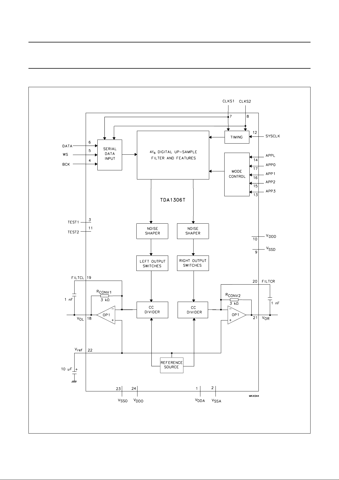
BLOCK DIAGRAM
Fig.1 Block diagram.
September 1994 4

Philips Semiconductors Preliminary specification
Noise shaping filter DAC TDA1306T
PINNING
SYMBOL PIN DESCRIPTION
V
DDA
V
SSA
TEST1 3 test input 1; pin should be connected
BCK 4 bit clock input
WS 5 word select input
DATA 6 data input
CLKS1 7 clock and format selection 1 input
CLKS2 8 clock and format selection 2 input
V
SSD
V
DDD
TEST2 11 test input 2; pin should be connected
SYSCLK 12 system clock input 256fs or 384f
APP3 13 application mode 3 input
APPL 14 application mode selection input
APP2 15 application mode 2 input
APP1 16 application mode 1 input
APP0 17 application mode 0 input
V
OL
FILTCL 19 capacitor for left channel 1st order
FILTCR 20 capacitor for right channel 1st order
V
OR
V
ref
V
SSO
V
DDO
1 analog supply voltage (+5 V)
2 analog ground
to ground
9 digital ground
10 digital supply voltage (+5 V)
to ground
s
18 left channel output
filter function; should be connected
between pins 19 and 18
filter function; should be connected
between pins 20 and 21
21 right channel output
22 internal reference voltage for output
channels; 0.5V
DDO
(typ.)
23 operational amplifier ground
24 operational amplifier supply voltage
Fig.2 Pin configuration.
September 1994 5

Philips Semiconductors Preliminary specification
Noise shaping filter DAC TDA1306T
FUNCTIONAL DESCRIPTION
The TDA1306T CMOS DAC incorporates an up-sampling
filter, a noise shaper, continuous calibrated current
sources and operational amplifiers.
System clock and data input format
The TDA1306T accommodates slave mode only.
Consequently, in all applications, the system devices must
provide the system clock. The system frequency is
selectable at pins CLKS1 and CLKS2 (see Table 1).
Table 1 Data input format and system clock.
CLKS1 CLKS2 DATA INPUT FORMAT
00I
2
S-bus 256f
0 1 LSB fixed 16 bits 384f
1 0 LSB fixed 18 bits 384f
1 1 LSB fixed 20 bits 384f
Device operation
The TDA1306T supports the following data input modes:
2
• I
S-bus with data word length of up to 20 bits
(f
= 256fs)
sys
• LSB fixed serial format with data word length of 16, 18
or 20 bits (f
= 384fs). As this format idles on the MSB
sys
it is necessary to know how many bits are being
transmitted.
The input formats are illustrated in Fig.9. Left and right
data channel words are time multiplexed.
SYSTEM CLOCK
NORMAL SPEED DOUBLE SPEED
s
s
s
s
128f
192f
192f
192f
s
s
s
s
When the APPL pin is held HIGH and APP3 is held LOW,
pins APP0, APP1 and APP2 form a microcontroller
interface. When the APPL pin is held LOW, pins APP0,
APP1, APP2 and APP3 form a pseudo-static application
(TDA1305T pin compatible).
P
SEUDO-STATIC APPLICATION MODE (APPL = LOGIC 0)
In this mode, the device operation is controlled by
pseudo-static application pins where:
APP0 = attenuation mode control
APP1 = double-speed mode control
APP2 = mute mode control
APP3 = de-emphasis mode control.
In the pseudo-static application mode the TDA1306T is pin
compatible with the TDA1305T slave mode. The
correspondence between TDA1306T pin number,
TDA1306T pin name, TDA1305T pin mnemonic and a
description of the effects is given in Table 2.
September 1994 6

Philips Semiconductors Preliminary specification
Noise shaping filter DAC TDA1306T
Table 2 Pseudo-static application mode.
PIN
MNEMONIC
APP0 17 ATSB 0 12 dB attenuation (from full scale) activated
APP1 16 DSMB 0 double-speed mode
APP2 15 MUSB 0 samples decrease to mute level
APP3 13 DEEM1 0 de-emphasis OFF (44.1 kHz)
MICROCONTROLLER APPLICATION MODE (APPL = LOGIC 1,
APP3 =
In this mode, the device operation is controlled by a set of
flags in an 8-bit mode control register. The 8-bit mode
control register is written by a microcontroller interface
where:
The correspondence between serial-to-parallel
conversion, mode control flags and a summary of the
effect of the control flags is given in Table 3. Figures 3 and
4 illustrate the mode set timing.
LOGIC 0).
APPL = logic 1
APP0 = Data
APP1 = Clock
APP2 = RAB
APP3 = logic 0.
PIN NUMBER
TDA1305T
FUNCTION
VALUE DESCRIPTION
(only if MUSB = logic 1)
1 full scale (only if MUSB = logic 1)
1 normal-speed mode
1 level according to ATSB
1 de-emphasis ON (44.1 kHz)
M
ICROCONTROLLER WRITE OPERATION SEQUENCE
The microcontroller write operation follows the following
sequence:
• APP2 is held LOW by the microcontroller
• Microcontroller data is clocked into the internal shift
register on the LOW-to-HIGH transition on pin APP1
• Data D7 to D0 is latched into the appropriate control
register on the LOW-to-HIGH transition of pin APP2
(APP1 = HIGH)
• If more data is clocked into the TDA1306T before the
LOW-to-HIGH transition on pin APP2 then only the last
8 bits are used
• If less data is clocked into the TDA1306T unpredictable
operation will result
• If the LOW-to-HIGH transition of pin APP2 occurs when
APP1 = LOW, the command will be disregarded.
Fig.3 Microcontroller timing.
September 1994 7

Philips Semiconductors Preliminary specification
Noise shaping filter DAC TDA1306T
MICROCONTROLLER WRITE OPERATION SEQUENCE (REPEAT
)
MODE
The same command can be repeated several times (e.g.
for fade function) by applying APP2 pulses as shown in
Fig.4. It should be noted that APP1 must stay HIGH
between APP2 pulses. A minimum pause of 22 ms is
necessary between any two step-up or step-down
commands.
Fig.4 Microcontroller timing (repeat mode).
Table 3 Microcontroller mode control register.
BIT POSITION FUNCTION DESCRIPTION ACTIVE LEVEL
D7 ATSB 12 dB attenuation
D6 DSMB double speed LOW
D5 MUSB mute LOW
D4 DEEM de-emphasis HIGH
D3 FS full scale HIGH
D2 INCR increment HIGH
D1 DECR decrement HIGH
D0 not applicable reserved not applicable
LOW
(from full scale)
September 1994 8

Philips Semiconductors Preliminary specification
Noise shaping filter DAC TDA1306T
Volume control
A digital level control is incorporated in the TDA1306T
which performs the function of soft mute and attenuation
(pseudo-static application mode) or soft mute, attenuation,
fade, increment and decrement (microcontroller
application mode). The volume control of both channels
can be varied in small step changes determined by the
value of the internal fade counter where:
audio level = counter × maximum level/120,
where the counter is a 7-bit binary number between 0 and
120. The time taken for mute to vary from 120 to 0 is
1/120fs. For example, when fs= 44.1 kHz, the time taken
is approximately 3 ms.
VOLUME CONTROL (PSEUDO-STATIC APPLICATION MODE)
In the pseudo-static application mode (APPL = logic 0) the
digital audio output level is controlled by APP0
(attenuation) and APP2 (mute) so only the final volume
levels full scale, 12 dB (attenuate) and mute (−infinity dB)
can be selected. The mute function has priority over the
attenuation function. Accordingly, if MUSB is LOW, the
state of ATSB has no effect. An example of volume control
in this application mode is illustrated in Fig.5.
Fig.5 Volume control (pseudo-static application mode).
September 1994 9

Philips Semiconductors Preliminary specification
Noise shaping filter DAC TDA1306T
VOLUME CONTROL (MICROCONTROLLER APPLICATION MODE)
In the microcontroller application mode (APPL = logic 1,
APP3 = logic 0) the audio output level is controlled by
volume control bits ATSB, MUSB, FS, INCR and DECR.
Mute is activated by sending the MUSB command to the
mode control register via the microcontroller interface. The
audio output level will be reduced to zero in a maximum of
120 steps (depending on the current position of the fade
counter) and taking a maximum of 3 ms. Mute, attenuation
and full scale are synchronized to prevent operation in the
middle of a word.
• The counter is preset to 120 by the full scale command.
• The counter is preset to 30 by the attenuate command
when its value is more then 30. If the value of the
counter is less than 30 dB the ATSB command has no
effect.
• The counter is preset to logic 0 by the mute command
MUSB.
• Attenuation (−12 dB) is activated by sending the ATSB
command to the fade control register (D7).
• Attenuation and mute are cancelled by sending the
full-scale command to the fade control register
(Register D3).
To control the fade counter in a continuous way, the
INCREMENT and DECREMENT commands are available
(fade control Registers D1 and D2). They will increment
and decrement the counter by 1 for each register write
operation. When issuing more than 1 step-up or step-down
command in sequence, the write repeat mode may be
used (see microcontroller application mode). An example
of volume control in this application mode is illustrated in
Fig.6.
(1) INCR and DECR in repeat mode.
Fig.6 Volume control (microcontroller application mode).
September 1994 10

Philips Semiconductors Preliminary specification
Noise shaping filter DAC TDA1306T
There are two recommended application situations within
the microcontroller mode:
• The customer wants to use the microcontroller interface
without the volume setting facility. In this event the
operation is as follows:
– Mute ON; by sending the MUSB command
– Mute OFF; by sending the FS command
– Attenuation ON; by sending the ATSB command
– Attenuation OFF; by sending the FS command.
It is possible to switch from ‘Attenuation ON’ to ‘Mute
ON’ but not vice-versa.
• Incorporating the volume control feature operates as
follows:
– Mute ON; by sending the MUSB command the
microcontroller has to store the previous volume
setting
– Mute OFF; by sending succeeding INCR commands
until the previous volume is reached
– Attenuation ON; by sending succeeding DECR
commands until a relative downstep of −12 dB is
reached. The microcontroller has to store the
previous volume
– Attenuation OFF; by sending the succeeding INCR
commands until the previous volume is reached
– Volume UP; by sending succeeding INCR
commands
– Volume DOWN; by sending succeeding DECR
commands.
De-emphasis
applied by means of an IIR filter. De-emphasis is
synchronized to prevent operation in the middle of a word.
Double-speed mode
The double-speed mode is controlled by the DSMB bit at
register D6 (microcontroller application mode) or by
activating the APP1 pin (pseudo-static application mode).
When the control bit is active LOW the device operates in
the double-speed mode.
Oversampling filter and noise shaper
The digital filter is a four times oversampling filter. It
consists of two sections which each increase the sample
rate by 2. The noise-shaper operates on 4f
and reduces
s
the in-band noise density.
DAC and operational amplifiers
In this noise shaping filter DAC a special data code and
bidirectional current sources are used in order to achieve
true low-noise performance. The special data code
guarantees that only small values of current flow to the
output during small signal passages while larger positive
or negative values are generated using the bidirectional
current sources. The noise shaping filter-DAC uses the
continuous calibration conversion technique.
The operational amplifiers and the internal conversion
resistors R
CONV1
and R
convert the DAC current to
CONV2
an output voltage available at VOL and VOR. Connecting an
external capacitor between FILTCL and VOL, FILTCR and
VOR respectively provides the required 1st-order post
filtering.
A digital de-emphasis is implemented in the TDA1306T.
By selecting the DEEM bit at register D4 (microcontroller
application mode) or activating the APP3 pin
(pseudo-static application mode), de-emphasis can be
September 1994 11

Philips Semiconductors Preliminary specification
Noise shaping filter DAC TDA1306T
LIMITING VALUES
In accordance with the Absolute Maximum Rating System (IEC 134).
SYMBOL PARAMETER CONDITIONS MIN. MAX. UNIT
V
DD
T
xtal
T
stg
T
amb
V
es
Notes
1. All V
2. Equivalent to discharging a 100 pF capacitor via a 1.5 kΩ series resistor.
3. Equivalent to discharging a 200 pF capacitor via a 2.5 mH series inductor.
supply voltage note 1 − 7.0 V
maximum crystal temperature − +150 °C
storage temperature −65 +125 °C
operating ambient temperature −40 +85 °C
electrostatic handling note2 −2000 +2000 V
note 3 −200 +200 V
and VSS connections must be made to the same power supply.
DD
THERMAL CHARACTERISTICS
SYMBOL PARAMETER VALUE UNIT
R
th j-a
thermal resistance from junction to ambient in free air 69 K/W
QUALITY SPECIFICATION
In accordance with
Handbook”
. The handbook can be ordered using the code 9398 510 63011.
“UZW-BO/FQ-0601”.
The numbers of the quality specification can be found in the
“Quality Reference
September 1994 12

Philips Semiconductors Preliminary specification
Noise shaping filter DAC TDA1306T
DC CHARACTERISTICS
V
DDD=VDDA=VDDO
specified.
SYMBOL PARAMETER CONDITIONS MIN. TYP. MAX. UNIT
V
DDD
V
DDA
V
DDO
I
DDD
I
DDA
I
DDO
P
tot
V
IH
V
IL
R
pd
|I
| input leakage current −−10 µA
LI
C
i
V
ref
R
CONV
V
FS(rms)
R
L
= 5 V; T
=25°C; all voltages referenced to ground (pins 2, 9 and 23); unless otherwise
amb
digital supply voltage (pin 10) note 1 4.5 5.0 5.5 V
analog supply voltage (pin 1) note 1 4.5 5.0 5.5 V
operational amplifier supply
note 1 4.5 5.0 5.5 V
voltage (pin 24)
digital supply current f
= 11.28 MHz − 58mA
sys
analog supply current at digital silence − 36mA
operational amplifier supply
current
total power dissipation f
no operational
amplifier load resistor
= 11.28 MHz; digital
sys
− 24mA
− 50 90 mW
silence; no operational
amplifier load resistor
HIGH level digital input voltage
0.7V
DDD
− V
DDD
+0.5V
(pins 3 to 8 and 11 to 17)
LOW level digital input voltage
−0.5 − 0.3V
DDD
V
(pins 3 to 8 and 11 to 17)
internal pull-down resistor to
V
(pins 3 and 11)
SSD
17 − 134 kΩ
input capacitance −−10 pF
reference voltage (pin 22) with respect to V
current-to-voltage conversion
SSO
0.45V
DDO
0.5V
DDO
0.55V
DDO
V
2.4 3.0 3.6 kΩ
resistor
full-scale output voltage (RMS
RL>5kΩ; note 2 0.935 1.1 1.265 V
value)
output load resistance 5 −−kΩ
Notes
1. All power supply pins (V
and VSS) must be connected to the same external power supply unit.
DD
2. RL is the AC resistance of the external circuitry connected to the audio outputs of the application circuit.
September 1994 13

Philips Semiconductors Preliminary specification
Noise shaping filter DAC TDA1306T
AC CHARACTERISTICS (ANALOG)
V
DDD=VDDA=VDDO
specified.
SYMBOL PARAMETER CONDITIONS MIN. TYP. MAX. UNIT
DACs
SVRR supply voltage ripple
∆G
v
α
ct
(THD + N)/S total harmonic distortion
S/N
ds
= 5 V; T
rejection V
=25°C; all voltages referenced to ground (pins 2, 9 and 23); unless otherwise
amb
and V
DDA
DDO
unbalance between the 2
DAC voltage outputs
(pins 18 and 21)
crosstalk between the 2 DAC
voltage outputs
(pins 18 and 21)
plus noise-to-signal ratio
signal-to-noise ratio at
digital silence
f
= 1 kHz;
ripple
V
= 100 mV (p-p);
ripple
− 40 − dB
C22 = 10 µF
maximum volume −−0.5 dB
one output digital silence
−−110 −85 dB
the other maximum volume
at 0 dB signal level;
f
= 1 kHz
i
at −60 dB signal level;
f
= 1 kHz
i
−−70 − dB
− 0.032 − %
−−42 −32 dB
− 0.8 2.5 %
no signal; A-weighted −−108 −96 dB
Operational amplifiers
G
v
PSRR power supply rejection ratio f
open-loop voltage gain − 85 − dB
= 3 kHz;
ripple
V
= 100 mV (p-p);
ripple
− 90 − dB
A-weighted
(THD + N)/S total harmonic distortion
plus noise-to-signal ratio
f
UG
|Z
| AC output impedance RL>5kΩ−1.5 150 Ω
o
unity gain frequency open loop − 4.5 − MHz
R
>5kΩ;fi= 1 kHz;
L
Vo= 2.8 V (p-p)
−−100 − dB
September 1994 14

Philips Semiconductors Preliminary specification
Noise shaping filter DAC TDA1306T
AC CHARACTERISTICS (DIGITAL)
V
DDD=VDDA=VDDO
otherwise specified.
SYMBOL PARAMETER CONDITIONS MIN. TYP. MAX. UNIT
T
WX
t
CWL
t
CWH
Serial input data timing (see Fig.8)
f
s
f
BCK
t
r
t
f
t
H
t
L
t
su
t
h
t
suWS
t
hWS
Microcontroller interface timing (see Fig.9)
t
L
t
H
t
suDC
t
hCD
t
suCR
4.5 to 5.5 V; all voltages referenced to ground (pins 2, 9 and 23); T
clock cycle time f
f
LOW level pulse width 22 −−ns
sys
f
HIGH level pulse width 22 −−ns
sys
word select input audio
sample frequency
clock input frequency
(data input rate)
= 384fs; normal speed 54.2 59.1 104 ns
sys
f
= 192fs; double speed 54.2 59.1 104 ns
sys
= 256fs; normal speed 81.3 88.6 156 ns
f
sys
f
= 128fs; double speed 81.3 88.6 156 ns
sys
normal speed 25 44.1 48 kHz
double speed 50 88.2 96 kHz
f
= 384fs; normal speed; note 1 −−64f
sys
f
= 192fs; double speed; note 1 −−64f
sys
= 256fs; normal speed −−64f
f
sys
f
= 128fs; double speed; note 2 −−48f
sys
= −40 to +85 °C; unless
amb
s
s
s
s
kHz
kHz
kHz
kHz
rise time −−20 ns
fall time −−20 ns
bit clock HIGH time 55 −−ns
bit clock LOW time 55 −−ns
data set-up time 20 −−ns
data hold time 10 −−ns
word select set-up time 20 −−ns
word select hold time 10 −−ns
input LOW time 2 −−µs
Input HIGH time 2 −−µs
set-up time DATA to CLOCK 1 −−µs
hold time CLOCK to DATA 1 −−µs
set-up time CLOCK to RAB 1 −−µs
Notes
1. A clock frequency of up to 96fs is possible in the event of a rising edge of BCK occurring during SYSCLK = LOW.
2. A clock frequency of up to 64fs is possible in the event of a rising edge of BCK occurring during SYSCLK = LOW.
September 1994 15

Philips Semiconductors Preliminary specification
Noise shaping filter DAC TDA1306T
September 1994 16
Fig.7 Data input formats.

Philips Semiconductors Preliminary specification
Noise shaping filter DAC TDA1306T
Fig.8 Timing of input signals.
Fig.9 Microcontroller timing.
September 1994 17

Philips Semiconductors Preliminary specification
Noise shaping filter DAC TDA1306T
TEST AND APPLICATION INFORMATION
Filter characteristics
Table 4 Digital filter specification (f
BAND ATTENUATION
0 to 19 kHz < 0.001 dB
19 to 20 kHz < 0.03 dB
24 kHz > 25 dB
25 to 35 kHz > 40 dB
35 to 64 kHz > 50 dB
64 to 68 kHz > 31 dB
68 kHz > 35 dB
69 to 88 kHz > 40 dB
= 44.1 kHz).
s
Table 5 Digital filter phase distortion (f
BAND PHASE DISTORTION
0 to 16 kHz < ±1°
= 44.1 kHz).
s
September 1994 18

Philips Semiconductors Preliminary specification
Noise shaping filter DAC TDA1306T
PACKAGE OUTLINE
handbook, full pagewidth
S
pin 1
index
112
0.9
0.4
(4x)
15.6
15.2
1.27
0.49
0.36
0.1 S
1324
0.25 M
(24x)
2.45
2.25
0.3
0.1
10.65
10.00
detail A
7.6
7.4
1.1
0.5
1.1
1.0
0.32
0.23
0 to 8
MBC235 - 1
A
2.65
2.35
o
Dimensions in mm.
Fig.10 Plastic small outline package; 24 leads; body width 7.5 mm (SO24; SOT137-1).
September 1994 19

Philips Semiconductors Preliminary specification
Noise shaping filter DAC TDA1306T
SOLDERING
Plastic small-outline packages
YWAVE
B
During placement and before soldering, the component
must be fixed with a droplet of adhesive. After curing the
adhesive, the component can be soldered. The adhesive
can be applied by screen printing, pin transfer or syringe
dispensing.
Maximum permissible solder temperature is 260 °C, and
maximum duration of package immersion in solder bath is
10 s, if allowed to cool to less than 150 °C within 6 s.
Typical dwell time is 4 s at 250 °C.
A modified wave soldering technique is recommended
using two solder waves (dual-wave), in which a turbulent
wave with high upward pressure is followed by a smooth
laminar wave. Using a mildly-activated flux eliminates the
need for removal of corrosive residues in most
applications.
Y SOLDER PASTE REFLOW
B
Reflow soldering requires the solder paste (a suspension
of fine solder particles, flux and binding agent) to be
applied to the substrate by screen printing, stencilling or
pressure-syringe dispensing before device placement.
Several techniques exist for reflowing; for example,
thermal conduction by heated belt, infrared, and
vapour-phase reflow. Dwell times vary between 50 and
300 s according to method. Typical reflow temperatures
range from 215 to 250 °C.
Preheating is necessary to dry the paste and evaporate
the binding agent. Preheating duration: 45 min at 45 °C.
EPAIRING SOLDERED JOINTS (BY HAND-HELD SOLDERING
R
IRON OR PULSE
-HEATED SOLDER TOOL)
Fix the component by first soldering two, diagonally
opposite, end pins. Apply the heating tool to the flat part of
the pin only. Contact time must be limited to 10 s at up to
300 °C. When using proper tools, all other pins can be
soldered in one operation within 2 to 5 s at between 270
and 320 °C. (Pulse-heated soldering is not recommended
for SO packages.)
For pulse-heated solder tool (resistance) soldering of VSO
packages, solder is applied to the substrate by dipping or
by an extra thick tin/lead plating before package
placement.
DEFINITIONS
Data sheet status
Objective specification This data sheet contains target or goal specifications for product development.
Preliminary specification This data sheet contains preliminary data; supplementary data may be published later.
Product specification This data sheet contains final product specifications.
Limiting values
Limiting values given are in accordance with the Absolute Maximum Rating System (IEC 134). Stress above one or
more of the limiting values may cause permanent damage to the device. These are stress ratings only and operation
of the device at these or at any other conditions above those given in the Characteristics sections of the specification
is not implied. Exposure to limiting values for extended periods may affect device reliability.
Application information
Where application information is given, it is advisory and does not form part of the specification.
LIFE SUPPORT APPLICATIONS
These products are not designed for use in life support appliances, devices, or systems where malfunction of these
products can reasonably be expected to result in personal injury. Philips customers using or selling these products for
use in such applications do so at their own risk and agree to fully indemnify Philips for any damages resulting from such
improper use or sale.
September 1994 20

Philips Semiconductors Preliminary specification
Noise shaping filter DAC TDA1306T
NOTES
September 1994 21

Philips Semiconductors Preliminary specification
Noise shaping filter DAC TDA1306T
NOTES
September 1994 22

Philips Semiconductors Preliminary specification
Noise shaping filter DAC TDA1306T
NOTES
September 1994 23

Philips Semiconductors – a worldwide company
Argentina: IEROD, Av. Juramento 1992 - 14.b, (1428)
BUENOS AIRES, Tel. (541)786 7633, Fax. (541)786 9367
Australia: 34 Waterloo Road, NORTH RYDE, NSW 2113,
Tel. (02)805 4455, Fax. (02)805 4466
Austria: Triester Str. 64, A-1101 WIEN, P.O. Box 213,
Tel. (01)60 101-1236, Fax. (01)60 101-1211
Belgium: Postbus 90050, 5600 PB EINDHOVEN, The Netherlands,
Tel. (31)40 783 749, Fax. (31)40 788 399
Brazil: Rua do Rocio 220 - 5
CEP: 04552-903-SÃO PAULO-SP, Brazil.
P.O. Box 7383 (01064-970).
Tel. (011)821-2333, Fax. (011)829-1849
Canada: PHILIPS SEMICONDUCTORS/COMPONENTS:
Tel. (800) 234-7381, Fax. (708) 296-8556
Chile: Av. Santa Maria 0760, SANTIAGO,
Tel. (02)773 816, Fax. (02)777 6730
Colombia: IPRELENSO LTDA, Carrera 21 No. 56-17,
77621 BOGOTA, Tel. (571)249 7624/(571)217 4609,
Fax. (571)217 4549
Denmark: Prags Boulevard 80, PB 1919, DK-2300 COPENHAGEN S,
Tel. (032)88 2636, Fax. (031)57 1949
Finland: Sinikalliontie 3, FIN-02630 ESPOO,
Tel. (9)0-50261, Fax. (9)0-520971
France: 4 Rue du Port-aux-Vins, BP317,
92156 SURESNES Cedex,
Tel. (01)4099 6161, Fax. (01)4099 6427
Germany: P.O. Box 10 63 23, 20043 HAMBURG,
Tel. (040)3296-0, Fax. (040)3296 213.
Greece: No. 15, 25th March Street, GR 17778 TAVROS,
Tel. (01)4894 339/4894 911, Fax. (01)4814 240
Hong Kong: PHILIPS HONG KONG Ltd., 6/F Philips Ind. Bldg.,
24-28 Kung Yip St., KWAI CHUNG, N.T.,
Tel. (852)424 5121, Fax. (852)428 6729
India: Philips INDIA Ltd, Shivsagar Estate, A Block ,
Dr. Annie Besant Rd. Worli, Bombay 400 018
Tel. (022)4938 541, Fax. (022)4938 722
Indonesia: Philips House, Jalan H.R. Rasuna Said Kav. 3-4,
P.O. Box 4252, JAKARTA 12950,
Tel. (021)5201 122, Fax. (021)5205 189
Ireland: Newstead, Clonskeagh, DUBLIN 14,
Tel. (01)640 000, Fax. (01)640 200
Italy: PHILIPS SEMICONDUCTORS S.r.l.,
Piazza IV Novembre 3, 20124 MILANO,
Tel. (0039)2 6752 2531, Fax. (0039)2 6752 2557
Japan: Philips Bldg 13-37 , Kohnan 2-chome, Minato-ku, TOKYO 108,
Tel. (03)3740 5028, Fax. (03)3740 0580
Korea: (Republic of) Philips House, 260-199 Itaewon-dong,
Yongsan-ku, SEOUL, Tel. (02)794-5011, Fax. (02)798-8022
Malaysia: No. 76 Jalan Universiti, 46200 PETALING JAYA,
SELANGOR, Tel. (03)750 5214, Fax. (03)757 4880
Mexico: 5900 Gateway East, Suite 200, EL PASO, TX 79905,
Tel. 9-5(800)234-7381, Fax. (708)296-8556
Netherlands: Postbus 90050, 5600 PB EINDHOVEN, Bldg. VB
Tel. (040)783749, Fax. (040)788399
New Zealand: 2 Wagener Place, C.P.O. Box 1041, AUCKLAND,
Tel. (09)849-4160, Fax. (09)849-7811
Norway: Box 1, Manglerud 0612, OSLO,
Tel. (022)74 8000, Fax. (022)74 8341
th
floor, Suite 51,
Pakistan: Philips Electrical Industries of Pakistan Ltd.,
Exchange Bldg. ST-2/A, Block 9, KDA Scheme 5, Clifton,
KARACHI 75600, Tel. (021)587 4641-49,
Fax. (021)577035/5874546.
Philippines: PHILIPS SEMICONDUCTORS PHILIPPINES Inc,
106 Valero St. Salcedo Village, P.O. Box 2108 MCC, MAKATI,
Metro MANILA, Tel. (02)810 0161, Fax. (02)817 3474
Portugal: PHILIPS PORTUGUESA, S.A.,
Rua dr. António Loureiro Borges 5, Arquiparque - Miraflores,
Apartado 300, 2795 LINDA-A-VELHA,
Tel. (01)4163160/4163333, Fax. (01)4163174/4163366.
Singapore: Lorong 1, Toa Payoh, SINGAPORE 1231,
Tel. (65)350 2000, Fax. (65)251 6500
South Africa: S.A. PHILIPS Pty Ltd.,
195-215 Main Road Martindale, 2092 JOHANNESBURG,
P.O. Box 7430 Johannesburg 2000,
Tel. (011)470-5911, Fax. (011)470-5494.
Spain: Balmes 22, 08007 BARCELONA,
Tel. (03)301 6312, Fax. (03)301 42 43
Sweden: Kottbygatan 7, Akalla. S-164 85 STOCKHOLM,
Tel. (0)8-632 2000, Fax. (0)8-632 2745
Switzerland: Allmendstrasse 140, CH-8027 ZÜRICH,
Tel. (01)488 2211, Fax. (01)481 77 30
Taiwan: PHILIPS TAIWAN Ltd., 23-30F, 66, Chung Hsiao West
Road, Sec. 1. Taipeh, Taiwan ROC, P.O. Box 22978,
TAIPEI 100, Tel. (02)388 7666, Fax. (02)382 4382.
Thailand: PHILIPS ELECTRONICS (THAILAND) Ltd.,
209/2 Sanpavuth-Bangna Road Prakanong,
Bangkok 10260, THAILAND,
Tel. (662)398-0141, Fax. (662)398-3319.
Turkey:Talatpasa Cad. No. 5, 80640 GÜLTEPE/ISTANBUL,
Tel. (0212)279 2770, Fax. (0212)269 3094
United Kingdom: Philips Semiconductors LTD.,
276 Bath road, Hayes, MIDDLESEX UB3 5BX,
Tel. (081)73050000, Fax. (081)7548421
United States:811 East Arques Avenue, SUNNYVALE,
CA 94088-3409, Tel. (800)234-7381, Fax. (708)296-8556
Uruguay: Coronel Mora 433, MONTEVIDEO,
Tel. (02)70-4044, Fax. (02)92 0601
For all other countries apply to: Philips Semiconductors,
International Marketing and Sales, Building BE-p,
P.O. Box 218, 5600 MD, EINDHOVEN, The Netherlands,
Telex 35000 phtcnl, Fax. +31-40-724825
SCD35 © Philips Electronics N.V. 1994
All rights are reserved. Reproduction in whole or in part is prohibited without the
prior written consent of the copyright owner.
The information presented in this document does not form part of any quotation
or contract, is believed to be accurate and reliable and may be changed without
notice. No liability will be accepted by the publisher for any consequence of its
use. Publication thereof does not convey nor imply any license under patent- or
other industrial or intellectual property rights.
Printed in The Netherlands
Philips Semiconductors
 Loading...