

Philips PCF8578H Datasheet
INTEGRATED CIRCUITS
DATA SH EET
PCF8578
LCD row/column driver for dot
matrix graphic displays
Product specification
Supersedes data of 1997 Mar 28
File under Integrated Circuits, IC12
1998 Sep 08

Philips Semiconductors Product specification
LCD row/column driver for dot matrix
graphic displays
CONTENTS
1 FEATURES
2 APPLICATIONS
3 GENERAL DESCRIPTION
4 ORDERING INFORMATION
5 BLOCK DIAGRAM
6 PINNING
7 FUNCTIONAL DESCRIPTION
7.1 Mixed mode
7.2 Row mode
7.3 Multiplexed LCD bias generation
7.4 Power-on reset
7.5 Internal clock
7.6 External clock
7.7 Timing generator
7.8 Row/column drivers
7.9 Display mode controller
7.10 Display RAM
7.11 Data pointer
7.12 Subaddress counter
7.13 I2C-bus controller
7.14 Input filters
7.15 RAM access
7.16 Display control
7.17 TEST pin
8I
8.1 Command decoder
9 CHARACTERISTICS OF THE I2C-BUS
9.1 Bit transfer
9.2 Start and stop conditions
9.3 System configuration
9.4 Acknowledge
10 LIMITING VALUES
11 HANDLING
12 DC CHARACTERISTICS
13 AC CHARACTERISTICS
14 APPLICATION INFORMATION
15 CHIP DIMENSIONS AND BONDING PAD
16 CHIP-ON GLASS INFORMATION
17 PACKAGE OUTLINE
2
C-BUS PROTOCOL
LOCATIONS
PCF8578
18 SOLDERING
18.1 Introduction
18.2 Reflow soldering
18.3 Wave soldering
18.3.1 LQFP
18.3.2 VSO
18.3.3 Method (LQFP and VSO)
18.4 Repairing soldered joints
19 DEFINITIONS
20 LIFE SUPPORT APPLICATIONS
21 PURCHASE OF PHILIPS I2C COMPONENTS
1998 Sep 08 2

Philips Semiconductors Product specification
LCD row/column driver for dot matrix
graphic displays
1 FEATURES
• Single chip LCD controller/driver
• Stand-alone or may be used with up to 32 PCF8579s
(40960 dots possible)
• 40 driver outputs, configurable as32⁄8,24⁄16,16⁄24 or
8
⁄32rows/columns
• Selectable multiplex rates; 1 : 8, 1 : 16, 1 : 24 or 1 : 32
• Externally selectable bias configuration, 5 or 6 levels
• 1280-bit RAM for display data storage and scratch pad
• Display memory bank switching
• Auto-incremented data loading across hardware
subaddress boundaries (with PCF8579)
• Provides display synchronization for PCF8579
• On-chip oscillator, requires only 1 external resistor
• Power-on reset blanks display
• Logic voltage supply range 2.5 to 6 V
• Maximum LCD supply voltage 9 V
• Low power consumption
2
C-bus interface
• I
• TTL/CMOS compatible
• Compatible with most microcontrollers
• Optimized pinning for single plane wiring in multiple
device applications (with PCF8579)
• Space saving 56-lead plastic mini-pack and 64 pin quad
flat pack
• Compatible with chip-on-glass technology.
PCF8578
2 APPLICATIONS
• Automotive information systems
• Telecommunication systems
• Point-of-sale terminals
• Computer terminals
• Instrumentation.
3 GENERAL DESCRIPTION
The PCF8578 is a low power CMOS LCD row/column
driver, designed to drive dot matrix graphic displays at
multiplex rates of 1 : 8, 1 : 16, 1 : 24 or 1 : 32. The device
has 40 outputs, of which 24 are programmable,
configurable as
The PCF8578 can function as a stand-alone LCD
controller/driver for use in small systems, or for larger
systems can be used in conjunction with up to
32 PCF8579s for which it has been optimized. Together
these two devices form a general purpose LCD dot matrix
driver chip set, capable of driving displays of up to
40960 dots. The PCF8578 is compatible with most
microcontrollers and communicates via a two-line
bidirectional bus (I2C-bus). Communication overheads are
minimized by a display RAM with auto-incremented
addressing and display bank switching.
32
⁄8,24⁄16,16⁄24 or8⁄32rows/columns.
4 ORDERING INFORMATION
TYPE NUMBER
NAME DESCRIPTION VERSION
PCF8578T VSO56 plastic very small outline package; 56 leads SOT190-1
PCF8578U/2 − chip with bumps in tray −
PCF8578H LQFP64 plastic low profile quad flat package; 64 leads; body 10 × 10 × 1.4 mm SOT314-2
1998 Sep 08 3
PACKAGE
Philips Semiconductors Product specification
LCD row/column driver for dot matrix
graphic displays
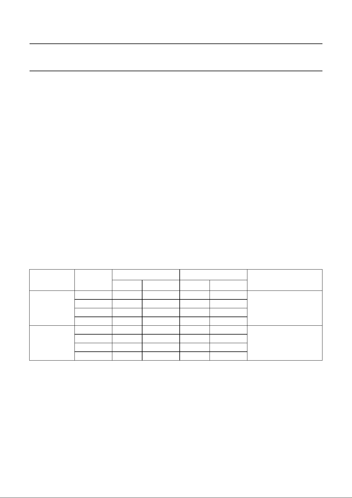
5 BLOCK DIAGRAM
9 (20)
V
DD
10 (21)
V
2
11 (22)
V
3
12 (23)
V
4
13 (24)
V
5
LCD
14 (25)
6 (12)
DISPLAY
MODE
CONTROLLER
V
TEST
C39 - C32
R31/C31 - R8/C8
R7 - R0
17 - 56
(29 to 35, 37, 38 to 46
48 to 62, 63, 64, 1 to 6)
ROW/COLUMN
DRIVERS
OUTPUT
CONTROLLER
PCF8578
(1)
PCF8578
SCL
SDA
POWER-ON
2 (8)
1 (7)
15, 16
RESET
INPUT
FILTERS
(14, 15, 17 to 19
26 to 28 36, 47)
n.c. n.c.
SUBADDRESS
COUNTER
2
I C-BUS
CONTROLLER
SA0
Y DECODER
AND SENSING
AMPLIFIERS
RAM DATA POINTER
7 (13)
32 x 40-BIT
DISPLAY RAM
X DECODER
YX
COMMAND
DECODER
DISPLAY
DECODER
TIMING
GENERATOR
OSCILLATOR
(9) 3
(10) 4
(16) 8
(11) 5
MSA842
R
SYNC
CLK
OSC
OSC
V
SS
(1) Operates at LCD voltage levels, all other blocks operate at logic levels.
The pin numbers given in parenthesis refer to the LQFP64 package.
Fig.1 Block diagram.
1998 Sep 08 4

Philips Semiconductors Product specification
LCD row/column driver for dot matrix
graphic displays
6 PINNING
SYMBOL
VSO56 LQFP64
SDA 1 7 I
SCL 2 8 I
SYNC 3 9 cascade synchronization output
CLK 4 10 external clock input/output
V
SS
5 11 ground (logic)
TEST 6 12 test pin (connect to V
SA0 7 13 I
OSC 8 16 oscillator input
V
V
V
DD
to V
2
LCD
5
9 20 positive supply voltage
10 to 13 21 to 24 LCD bias voltage inputs
14 25 LCD supply voltage
n.c. 15, 16 14, 15, 17 to 19,
C39 to C32 17 to 24 29 to 35, 37 LCD column driver outputs
R31/C31 to R8/C8 25 to 48 38 to 46, 48 to 62 LCD row/column driver outputs
R7 to R0 49 to 56 63, 64, 1 to 6 LCD row driver outputs
PIN
26 to 28, 36, 47
DESCRIPTION
2
C-bus serial data input/output
2
C-bus serial clock input
)
SS
2
C-bus slave address input (bit 0)
not connected
PCF8578
1998 Sep 08 5
Philips Semiconductors Product specification
LCD row/column driver for dot matrix
graphic displays
SDA
1
2
SCL
SYNC
3
CLK
4
V
5
SS
TEST
6
SA0
7
OSC
8
V
9
DD
V
10
2
V
11
3
V
12
4
V
5
13
V
14
LCD
n.c.
n.c.
C39
C38
C37
C36
C35
C34
C33
C32
R31/C31
R30/C30
R29/C29
R28/C28
15
16
17
18
19
20
21
22
23
24
25
26
27
28
PCF8578
56
55
54
53
52
51
50
49
48
47
46
45
44
43
42
41
40
39
38
37
36
35
34
33
32
31
30
29
PCF8578
R0
R1
R2
R3
R4
R5
R6
R7
R8/C8
R9/C9
R10/C10
R11/C11
R12/C12
R13/C13
R14/C14
R15/C15
R16/C16
R17/C17
R18/C18
R19/C19
R20/C20
R21/C21
R22/C22
R23/C23
R24/C24
R25/C25
R26/C26
R27/C27
Fig.2 Pin configuration (VSO56).
1998 Sep 08 6
MSA839
Philips Semiconductors Product specification
LCD row/column driver for dot matrix
graphic displays
handbook, full pagewidth
R6
R5
R4
R3
R2
R1
R0
SDA
SCL
SYNC
CLK
V
SS
TEST
SA0
n.c.
n.c.
OSC
R7
64
63
1
2
3
4
5
6
7
8
9
10
11
12
13
14
15
16
R8/C8
62
R9/C9
61
R11/C11
R10/C10
60
59
R13/C13
R12/C12
58
57
PCF8578
R15/C15
R14/C14
56
55
R17/C17
R16/C16
54
53
R19/C19
R18/C18
52
51
R21/C21
R20/C20
50
49
48
47
46
45
44
43
42
41
40
39
38
37
36
35
34
33
PCF8578
R22/C22
n.c.
R23/C23
R24/C24
R25/C25
R26/C26
R27/C27
R28/C28
R29/C29
R30/C30
R31/C31
C32
n.c.
C33
C34
C35
17
18
19
20
21
22
23
n.c.
n.c.
n.c.
DD
V
Fig.3 Pin configuration (LQFP64).
1998 Sep 08 7
24
25
26
27
28
29
30
31
32
5V4V3V2
V
LCD
V
n.c.
n.c.
n.c.
C39
C38
C37
MBH588
C36
Philips Semiconductors Product specification
LCD row/column driver for dot matrix
graphic displays
7 FUNCTIONAL DESCRIPTION
The PCF8578 row/column driver is designed for use in one
of three ways:
• Stand-alone row/column driver for small displays
(mixed mode)
• Row/column driver with cascaded PCF8579s
(mixed mode)
• Row driver with cascaded PCF8579s (mixed mode).
7.1 Mixed mode
In mixed mode, the device functions as both a row and
column driver. It can be used in small stand-alone
applications, or for larger displays with up to 15 PCF8579s
(31 PCF8579s when two slave addresses are used).
See Table 1 for common display configurations.
7.2 Row mode
In row mode, the device functions as a row driver with up
to 32 row outputs and provides the clock and
synchronization signals for the PCF8579. Up to 16
PCF8579s can normally be cascaded (32 when two slave
addresses are used).
PCF8578
Timing signals are derived from the on-chip oscillator,
whose frequency is determined by the value of the resistor
connected between OSC and V
Commands sent on the I2C-bus from the host
microcontroller set the mode (row or mixed), configuration
(multiplex rate and number of rows and columns) and
control the operation of the device. The device may have
one of two slave addresses. The only difference between
these slave addresses is the least significant bit, which is
set by the logic level applied to SA0. The PCF8578 and
PCF8579 also have subaddresses. The subaddress of the
PCF8578 is only defined in mixed mode and is fixed at 0.
The RAM may only be accessed in mixed mode and data
is loaded as described for the PCF8579.
Bias levels may be generated by an external potential
divider with appropriate decoupling capacitors. For large
displays, bias sources with high drive capability should be
used. A typical mixed mode system operating with up to
15 PCF8579s is shown in Fig.5 (a stand-alone system
would be identical but without the PCF8579s).
SS
.
Table 1 Possible displays configurations
APPLICATION
MULTIPLEX
RATE
MIXED MODE ROW MODE
TYPICAL APPLICATIONS
ROWS COLUMNS ROWS COLUMNS
Stand alone 1 : 8 8 32 −−small digital or
1:16 16 24 −−
alphanumerical displays
1:24 24 16 −−
1:32 32 8 −−
With PCF8579 1 : 8 8
1:16 16
1:24 24
1:32 32
(1)
(1)
(1)
(1)
632
624
616
608
(1)
(1)
(1)
(1)
8 × 44
16 × 2
(2)
24
(2)
24
(2)
(2)
640
640
640
640
(2)
(2)
(2)
(2)
alphanumeric displays and
dot matrix graphic displays
Notes
1. Using 15 PCF8579s.
2. Using 16 PCF8579s.
1998 Sep 08 8
Philips Semiconductors Product specification
LCD row/column driver for dot matrix
graphic displays
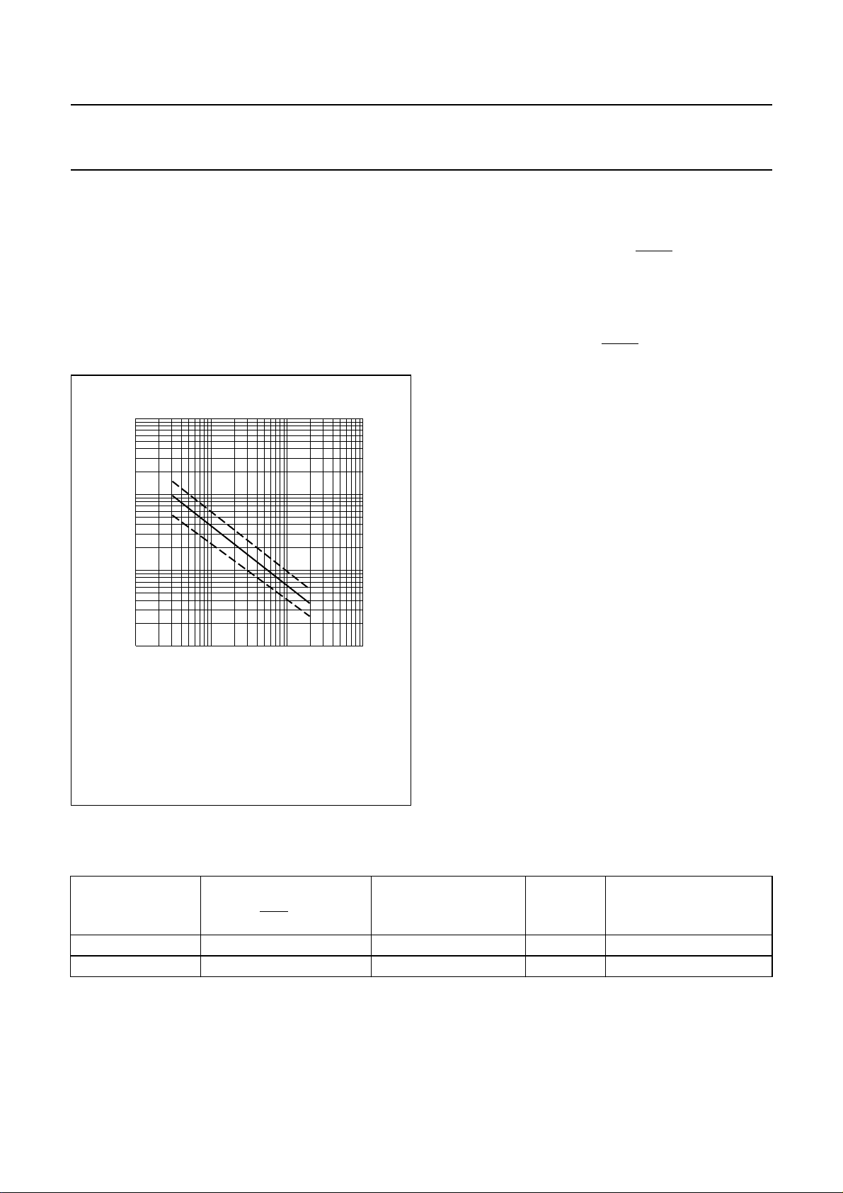
7.3 Multiplexed LCD bias generation
The bias levels required to produce maximum contrast
depend on the multiplex rate and the LCD threshold
voltage (Vth). Vth is typically defined as the RMS voltage at
which the LCD exhibits 10% contrast. Table 2 shows the
optimum voltage bias levels for the PCF8578 as functions
of Vop(Vop=VDD− V
ratios (D) for the different multiplex rates. A practical value
for Vop is obtained by equating V
shows the first 4 rows of Table 2 as graphs. Table 3 shows
the relative values of the resistors required in the
configuration of Fig.5 to produce the standard multiplex
rates.
Table 2 Optimum LCD voltages
PARAMETER
V
2
--------V
op
V
3
--------V
op
V
4
--------V
op
V
5
--------V
op
V
off rms()
----------------------V
op
V
on rms()
---------------------- V
op
V
on rms()
=
D
----------------------V
off rms()
), together with the discrimination
LCD
with Vth. Figure 4
off(rms)
MULTIPLEX RATE
1:8 1:16 1:24 1:32
0.739 0.800 0.830 0.850
0.522 0.600 0.661 0.700
0.478 0.400 0.339 0.300
0.261 0.200 0.170 0.150
0.297 0.245 0.214 0.193
0.430 0.316 0.263 0.230
1.447 1.291 1.230 1.196
PCF8578
7.4 Power-on reset
At power-on the PCF8578 resets to a defined starting
condition as follows:
1. Display blank
2. 1 : 32 multiplex rate, row mode
3. Start bank, 0 selected
4. Data pointer is set to X, Y address 0, 0
5. Character mode
6. Subaddress counter is set to 0
7. I2C-bus interface is initialized.
2
Data transfers on the I
following power-on, to allow completion of the reset action.
1.0
V
bias
V
op
0.8
0.6
0.4
0.2
0
V
Fig.4 V
, V3, V4, V5. See Table 2.
bias=V2
bias/Vop
C-bus should be avoided for 1 ms
MSA838
V
2
V
3
V
4
V
5
1:8 1:16 1:32
1:24
multiplex rate
as a function of the multiplex rate.
V
---------
V
op
th
3.370 4.080 4.680 5.190
Table 3 Multiplex rates and resistor values for Fig.5
MULTIPLEX RATE (n)
RESISTORS
n = 8 n = 16, 24, 32
R1 R R
R2 R
R3
n2–()R
3n–()R n3–()R
1998 Sep 08 9
This text is here in white to force landscape pages to be rotated correctly when browsing through the pdf in the Acrobat reader.This text is here in
_white to force landscape pages to be rotated correctly when browsing through the pdf in the Acrobat reader.This text is here inThis text is here in
white to force landscape pages to be rotated correctly when browsing through the pdf in the Acrobat reader. white to force landscape pages to be ...
1998 Sep 08 10
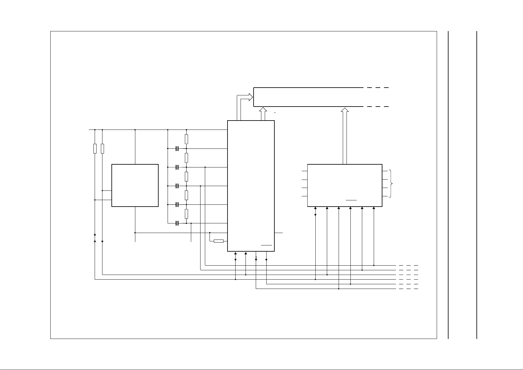
LCD DISPLAY
Philips Semiconductors Product specification
LCD row/column driver for dot matrix
graphic displays
n
rows
V
DD
R1
C
R2
C
HOST
MICROCONTROLLER
SCL
SDA
V
SS
R3
C
R2
C
R1
C
V
LCD
R
OSC
V
DD
V
2
V
3
V
4
V
5
V
LCD
V
SS
OSC
PCF8578
SCLSDA
SA0
CLK SYNC
40 n
columns
VSSV
VSSVDD/
40
columns
V
V
V
LCD
V
/
DD
SS
DD
V
V
SA0
SDA
DD
LCD
SS
SCL
PCF8579
CLK SYNC
A0
A1
subaddress 1
A2
A3
V
V
3
4
VSSVDD/
MSA843
PCF8578
Fig.5 Typical mixed mode configuration.

Philips Semiconductors Product specification
LCD row/column driver for dot matrix
graphic displays
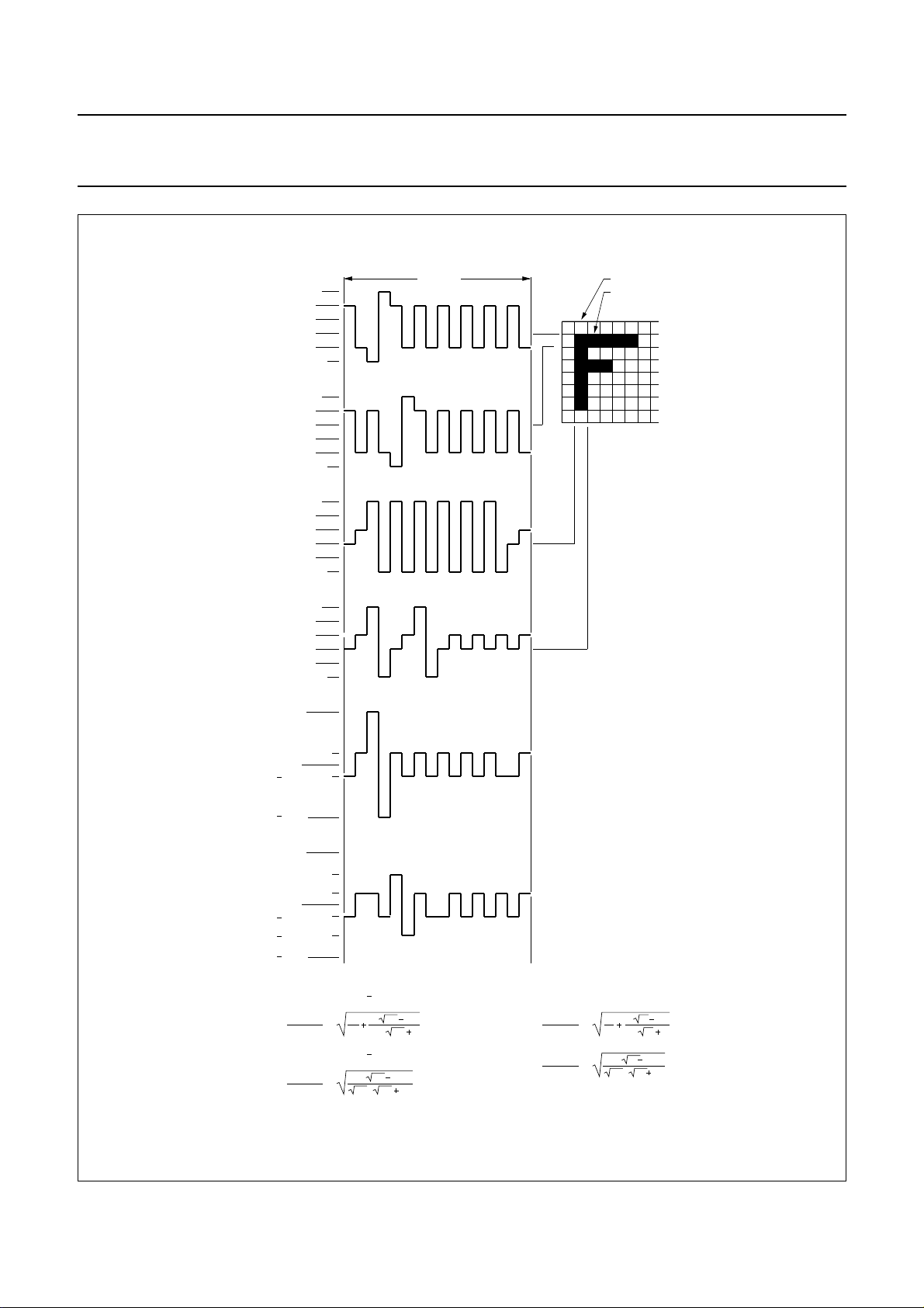
T
0 1 2 3 4 5 67
0 1 2 3 4 5 6 7 8 9 1011 12 13 14 15 16 17 18 19 20 21 22 23 24 25 26 27 28 29 30 31
ROW 0
COLUMN
ROW 0
COLUMN
ROW 0
COLUMN
ROW 0
COLUMN
V
DD
V
2
V
3
V
4
V
5
V
LCD
V
DD
V
2
V
3
V
4
V
5
V
LCD
SYNC
V
DD
V
2
V
3
V
4
V
5
V
LCD
V
DD
V
2
V
3
V
4
V
5
V
LCD
SYNC
V
DD
V
2
V
3
V
4
V
5
V
LCD
V
DD
V
2
V
3
V
4
V
5
V
LCD
SYNC
V
DD
V
2
V
3
V
4
V
5
V
LCD
V
DD
V
2
V
3
V
4
V
5
V
LCD
SYNC
frame
PCF8578
ON
OFF
1:8
15
14131211109876543210
1:16
23222120191817161514131211109876543210
1:24
1:32
column
MSA841
display
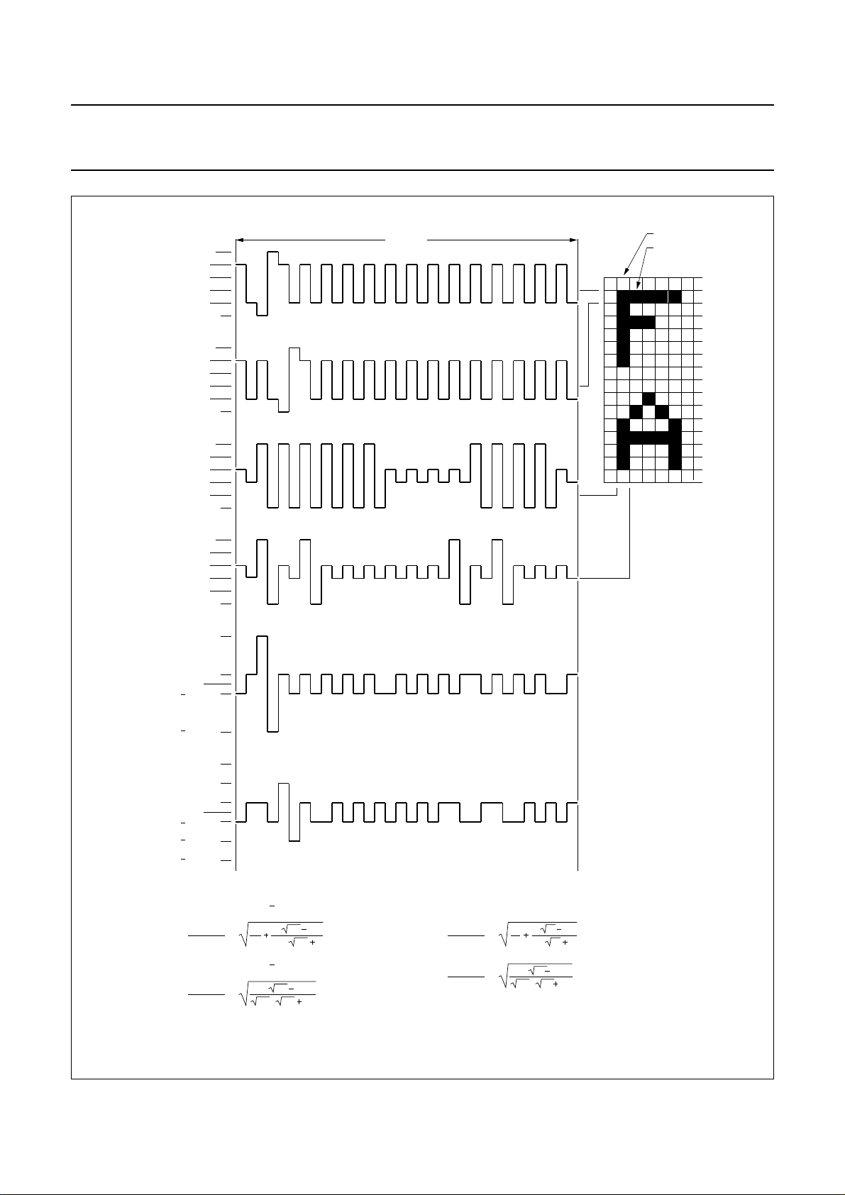
Fig.6 LCD row/column waveforms.
1998 Sep 08 11
Philips Semiconductors Product specification
LCD row/column driver for dot matrix
graphic displays
T
frame
ROW 1
R1 (t)
ROW 2
R2 (t)
COL 1
C1 (t)
V
V
V
V
V
V
V
V
V
V
V
V
V
V
V
V
V
V
DD
2
3
4
5
LCD
DD
2
3
4
5
LCD
DD
2
3
4
5
LCD
state 1 (OFF)
state 2 (ON)
dot matrix
1:8 multiplex rate
PCF8578
V
state 1
V
state 2
COL 2
C2 (t)
(t)
(t)
V
DD
V
2
V
3
V
4
V
5
V
LCD
V
op
0.261 V
0 V
0.261 V
V
op
V
op
0.478 V
0.261 V
0 V
0.261 V
0.478 V
V
op
V
state 1
V
on(rms)
V
op
V
state 2
V
off(rms)
V
op
op
op
op
op
op
op
(t) =C1(t) R1(t):
1
=
8
8
(t) = C2(t) R2(t):
()
8 1
2
=
()
8
8 1
=
8 1
=
0.297
2
0.430
()
8 1
MSA840
general relationship (n = multiplex rate)
V
on(rms)
V
op
V
off(rms)
V
op
=
=
1
n
()
n
n
n
()
n
1
2
()
n
n
1
1
1
2
Fig.7 LCD drive mode waveforms for 1 : 8 multiplex rate.
1998 Sep 08 12
Philips Semiconductors Product specification
LCD row/column driver for dot matrix
graphic displays
T
frame
ROW 1
R1 (t)
ROW 2
R2 (t)
COL 1
C1 (t)
COL 2
C2 (t)
V
V
V
V
V
V
V
V
V
V
V
V
V
V
V
V
V
V
V
V
V
V
V
V
DD
2
3
4
5
LCD
DD
2
3
4
5
LCD
DD
2
3
4
5
LCD
DD
2
3
4
5
LCD
PCF8578
state 1 (OFF)
state 2 (ON)
dot matrix
1:16 multiplex rate
V
state 1
V
state 2
V
op
0.2 V
0 V
0.2 V
V
op
V
op
0.6 V
0.2 V
0 V
0.2 V
0.6 V
V
op
V
state 1
V
on(rms)
V
state 2
V
off(rms)
op
op
op
op
op
op
V
op
V
op
(t) = C1(t) R1(t):
1
16
16
16 1
()
=
(t) = C2(t) R2(t):
()
16 1
2
=
()
16 1
16
16 1
MSA836
general relationship (n = multiplex rate)
V
=
0.316
=
0.254
2
on(rms)
V
op
V
off(rms)
V
op
=
=
1
n
()
n
n
n
()
n
1
2
()
n
n
1
1
1
2
(t)
(t)
Fig.8 LCD drive mode waveforms for 1 : 16 multiplex rate.
1998 Sep 08 13
Philips Semiconductors Product specification
LCD row/column driver for dot matrix
graphic displays
7.5 Internal clock
The clock signal for the system may be generated by the
internal oscillator and prescaler. The frequency is
determined by the value of the resistor R
For normal use a value of 330 kΩ is recommended.
The clock signal, for cascaded PCF8579s, is output at CLK
and has a frequency1⁄6 (multiplex rate 1 : 8, 1 : 16 and
1 : 32) or1⁄8 (multiplex rate 1 : 24) of the oscillator
frequency.
3
10
f
OSC
(kHz)
2
10
10
1
10
To avoid capacitive coupling, which could adversely affect oscillator
stability, R
pin. If this proves to be a problem, a filtering capacitor may be
connected in parallel to R
should be placed as closely as possible to the OSC
OSC
10
OSC
2
.
3
10
Fig.9 Oscillator frequency as a function of
external oscillator resistor, R
, see Fig.9.
OSC
MSA837
4
R(kΩ)
OSC
OSC
10
.
PCF8578
7.6 External clock
If an external clock is used, OSC must be connected to
VDD and the external clock signal to CLK. Table 4
summarizes the nominal CLK and SYNC frequencies.
7.7 Timing generator
The timing generator of the PCF8578 organizes the
internal data flow of the device and generates the LCD
frame synchronization pulse
integer multiple of the clock period. In cascaded
applications, this signal maintains the correct timing
relationship between the PCF8578 and PCF8579s in the
system.
7.8 Row/column drivers
Outputs R0 to R7 and C32 to C39 are fixed as row and
column drivers respectively. The remaining 24 outputs
R8/C8 to R31/C31 are programmable and may be
configured (in blocks of 8) to be either row or column
drivers. The row select signal is produced sequentially at
each output from R0 up to the number defined by the
multiplex rate (see Table 1). In mixed mode the remaining
outputs are configured as columns. In row mode all
programmable outputs (R8/C8 to R31/C31) are defined as
row drivers and the outputs C32 to C39 should be left
open-circuit.
Using a 1 : 16 multiplex rate, two sets of row outputs are
driven, thus facilitating split-screen configurations, i.e. a
row select pulse appears simultaneously at R0 and
R16/C16, R1 and R17/C17 etc. Similarly, using a multiplex
rate of 1 : 8, four sets of row outputs are driven
simultaneously. Driver outputs must be connected directly
to the LCD. Unused outputs should be left open-circuit.
In 1 : 8 R0 to R7 are rows; in 1 : 16 R0 to R15/C15 are
rows; in 1 : 24 R0 to R23/C23 are rows; in 1 : 32
R0 to R31/C31 are rows.
SYNC, whose period is an
Table 4 Signal frequencies required for nominal 64 Hz frame frequency; note 1.
OSCILLATOR
FREQUENCY
(2)
f
OSC
(Hz)
FRAME FREQUENCY
f
(Hz)
SYNC
MULTIPLEX RATE (n)
DIVISION
RATIO
12288 64 1 : 8, 1 : 16, 1 : 32 6 2048
12288 64 1 : 24 8 1536
Notes
1. A clock signal must always be present, otherwise the LCD may be frozen in a DC state.
2. R
OSC
= 330 kΩ.
1998 Sep 08 14
CLOCK FREQUENCY
f
(Hz)
CLK
 Loading...