

Philips PCF8577CP-F2, PCF8577CP-F3, PCF8577CT-F2, PCF8577CT-F3, PCF8577CU-10-F2 Datasheet
...
DATA SH EET
Product specification
Supersedes data of 1997 Mar 28
File under Integrated Circuits, IC12
1998 Jul 30
INTEGRATED CIRCUITS
PCF8577C
LCD direct/duplex driver with
I
2
C-bus interface

1998 Jul 30 2
Philips Semiconductors Product specification
LCD direct/duplex driver with
I
2
C-bus interface
PCF8577C
CONTENTS
1 FEATURES
2 GENERAL DESCRIPTION
3 ORDERING INFORMATION
4 BLOCK DIAGRAM
5 PINNING
6 FUNCTIONAL DESCRIPTION
6.1 Hardware subaddress A0, A1, A2
6.2 Oscillator A0/OSC
6.3 User-accessible registers
6.4 Auto-incremented loading
6.5 Direct drive mode
6.6 Duplex mode
6.7 Power-on reset
6.8 Slave address
6.9 I2C-bus protocol
6.10 Display memory mapping
7 CHARACTERISTICS OF THE I2C-BUS
7.1 Bit transfer
7.2 Start and stop conditions
7.3 System configuration
7.4 Acknowledge
8 LIMITING VALUES
9 HANDLING
10 DC CHARACTERISTICS
11 AC CHARACTERISTICS
12 APPLICATION INFORMATION
13 CHIP DIMENSIONS AND BONDING PAD
LOCATIONS
14 PACKAGE OUTLINES
15 SOLDERING
15.1 Plastic dual in-line packages
15.1.1 By dip or wave
15.1.2 Repairing soldered joints
15.2 Plastic small outline packages
15.2.1 By wave
15.2.2 By solder paste reflow
15.2.3 Repairing soldered joints (by hand-held
soldering iron or pulse-heated solder tool)
16 DEFINITIONS
17 LIFE SUPPORT APPLICATIONS
18 PURCHASE OF PHILIPS I2C COMPONENTS
1998 Jul 30 3
Philips Semiconductors Product specification
LCD direct/duplex driver with
I
2
C-bus interface
PCF8577C
1 FEATURES
• Direct/duplex drive modes with up to
32/64 LCD-segment drive capability per device
• Operating supply voltage: 2.5 to 6 V
• Low power consumption
• I2C-bus interface
• Optimized pinning for single plane wiring
• Single-pin built-in oscillator
• Auto-incremented loading across device subaddress
boundaries
• Display memory switching in direct drive mode
• May be used as I
2
C-bus output expander
• System expansion up to 256 segments
• Power-on reset blanks display
• I2C-bus address: 0111 0100.
2 GENERAL DESCRIPTION
The PCF8577C is a single chip, silicon gate CMOS circuit.
It is designed to drive liquid crystal displays with up to
32 segments directly, or 64 segments in a duplex
configuration.
The two-line I
2
C-bus interface substantially reduces wiring
overheads in remote display applications. I2C-bus traffic is
minimized in multiple IC applications by automatic address
incrementing, hardware subaddressing and display
memory switching (direct drive mode).To allow partial V
DD
shutdown the ESD protection system of the SCL and SDA
pins does not use a diode connected to VDD.
3 ORDERING INFORMATION
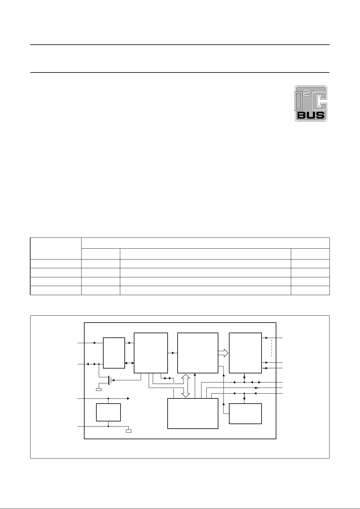
4 BLOCK DIAGRAM
TYPE NUMBER
PACKAGE
NAME DESCRIPTION VERSION
PCF8577CP DIP40 plastic dual in-line package; 40 leads (600 mil) SOT129-1
PCF8577CT VSO40 plastic very small outline package; 40 leads SOT158A
PCF8577CT − VS040 in blister tape −
PCF8577CU/10 − chip on film-frame-carrier (FFC) −
Fig.1 Block diagram.
MGA727
V
DD
V
SS
SDA
SCL
A0/OSC
A1
A2/BP2
BP1
S32
S1
PCF8577C
2
I C - BUS
CONTROLLER
INPUT
FILTERS
SEGMENT BYTE
REGISTERS
AND
MULTIPLEX
LOGIC
BACKPLANE
AND
SEGMENT
DRIVERS
CONTROL REGISTER
AND
COMPARATOR
OSCILLATOR
AND
DIVIDER
POWER -
ON
RESET
33
32
1
34
36
37
2
I C - BUS
40
39
35
38
1998 Jul 30 4
Philips Semiconductors Product specification
LCD direct/duplex driver with
I
2
C-bus interface
PCF8577C
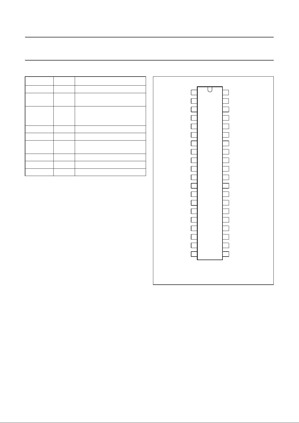
5 PINNING
SYMBOL PIN DESCRIPTION
S32 to S1 1 to 32 segments outputs
BP1 33 cascade sync input/backplane
output
A2/BP2 34 hardware address line and
cascade sync input/backplane
output
V
DD
35 positive supply voltage
A1 36 hardware address line input
A0/OSC 37 hardware address line and
oscillator pin input
V
SS
38 negative supply voltage
SCL 39 I
2
C-bus clock line input
SDA 40 I
2
C-bus data line input/output
Fig.2 Pin configuration.
1
2
3
4
5
6
7
8
9
10
11
12
13
40
39
38
37
36
35
34
33
32
31
30
29
28
2714
15
16
17
18
19
20
21
22
23
24
25
26
MGA725
V
DD
V
SS
SDA
SCL
A0/OSC
A1
A2/BP2
BP1
S32
S31
S30
S29
S28
S27
S26
S25
S24
S23
S22
S21
S20
S19
S18
S17
S16
S15
S14
S13
S1
S2
S3
S4
S5
S6
S7
S8
S9
S10
S11
S12
PCF8577C

1998 Jul 30 5
Philips Semiconductors Product specification
LCD direct/duplex driver with
I
2
C-bus interface
PCF8577C
6 FUNCTIONAL DESCRIPTION
6.1 Hardware subaddress A0, A1, A2
The hardware subaddress lines A0, A1 and A2 are used to
program the device subaddress for each PCF8577C
connected to the I
2
C-bus. Lines A0 and A2 are shared with
OSC and BP2 respectively to reduce pin-out
requirements.
1. Line A0 is defined as LOW (logic 0) when this pin is
used for the local oscillator or when connected to VSS.
Line A0 is defined as HIGH (logic 1) when connected
to VDD.
2. Line A1 must be defined as LOW (logic 0) or as HIGH
(logic 1) by connection to VSS or VDD respectively.
3. In the direct drive mode the second backplane signal
BP2 is not used and the A2/BP2 pin is exclusively the
A2 input. Line A2 is defined as LOW (logic 0) when
connected to VSS or, if this is not possible, by leaving
it unconnected (internal pull-down). Line A2 is defined
as HIGH (logic 1) when connected to VDD.
4. In the duplex drive mode the second backplane signal
BP2 is required and the A2 signal is undefined. In this
mode device selection is made exclusively from
lines A0 and A1.
6.2 Oscillator A0/OSC
The PCF8577C has a single-pin built-in oscillator which
provides the modulation for the LCD segment driver
outputs. One external resistor and one external capacitor
are connected to the A0/OSC pin to form the oscillator (see
Figs 15 and 16). For correct start-up of the oscillator after
power on, the resistor and capacitor must be connected to
the same V
SS/VDD
as the chip. In an expanded system
containing more than one PCF8577C the backplane
signals are usually common to all devices and only one
oscillator is required. The devices which are not used for
the oscillator are put into the cascade mode by connecting
the A0/OSC pin to either VDD or VSS depending on the
required state for A0. In the cascade mode each
PCF8577C is synchronized from the backplane signal(s).
6.3 User-accessible registers
There are nine user-accessible 1-byte registers. The first
is a control register which is used to control the loading of
data into the segment byte registers and to select display
options. The other eight are segment byte registers, split
into two banks of storage, which store the segment data.
The set of even numbered segment byte registers is called
BANK A. Odd numbered segment byte registers are called
BANK B.
There is one slave address for the PCF8577C (see Fig.6).
All addressed devices load the second byte into the control
register and each device maintains an identical copy of the
control byte in the control register at all times (see I2C-bus
protocol, Fig.7), i.e. all addressed devices respond to
control commands sent on the I2C-bus.
The control register is shown in more detail in Fig.3.
The least-significant bits select which device and which
segment byte register is loaded next. This part of the
register is therefore called the Segment Byte Vector
(SBV).
The upper three bits of the SBV (V5 to V3) are compared
with the hardware subaddress input signals A2, A1
and A0. If they are the same then the device is enabled for
loading, if not the device ignores incoming data but
remains active.
The three least-significant bits of the SBV (V2 to V0)
address one of the segment byte registers within the
enabled chip for loading segment data.
The control register also has two display control bits.
These bits are named MODE and BANK. The MODE bit
selects whether the display outputs are configured for
direct or duplex drive displays. The BANK bit allows the
user to display BANK A or BANK B.
6.4 Auto-incremented loading
After each segment byte is loaded the SBV is incremented
automatically. Thus auto-incremented loading occurs if
more than one segment byte is received in a data transfer.
Since the SBV addresses both device and segment
registers in all addressed chips, auto-incremented loading
may proceed across device boundaries provided that the
hardware subaddresses are arranged contiguously.

1998 Jul 30 6
Philips Semiconductors Product specification
LCD direct/duplex driver with
I
2
C-bus interface
PCF8577C
Fig.3 PCF8577C register organization.
MGA733
msb lsbmsb lsb
0
2
4
6
1
3
5
7
V5
V4 V3 V2 V1 V0
CONTROL REGISTER SEGMENT BYTE REGISTERS
BANK 'A'
BANK 'B'
DISPLAY
CONTROL
SEGMENT BYTE VECTOR
(SBV)
segment byte
register
address
comparison
A2 A1 A0
device
subaddress
(1) (1)
0 BANK 'A'
1 BANK 'B'
BANK
DISPLAY
MODE
0 DIRECT DRIVE
1 DUPLEX DRIVE
(1) Bits ignored in duplex mode.
Fig.4 Direct drive mode display output waveforms.
V
on(rms)=VDD
− VSS; V
off(rms)
=0.
MGA737
V
DD
V
SS
V
DD
V
SS
SSDD
V V
0
SSDD
(V V )
BP1 Sx
Segment x
(Sx)
BP1
1
f
LCD
OFF ON

1998 Jul 30 7
Philips Semiconductors Product specification
LCD direct/duplex driver with
I
2
C-bus interface
PCF8577C
6.5 Direct drive mode
The PCF8577C is set to the direct drive mode by loading
the MODE control bit with logic 0. In this mode only four
bytes are required to store the data for the 32 segment
drivers. Setting the BANK bit to logic 0 selects even bytes
(BANK A), setting the BANK bit to logic 1 selects odd bytes
(BANK B).
In the direct drive mode the SBV is auto-incremented by
two after the loading of each segment byte register. This
means that auto-incremented loading of BANK A or
BANK B is possible. Either bank may be completely or
partially loaded irrespective of which bank is being
displayed. Direct drive output waveforms are shown in
Fig.4.
6.6 Duplex mode
The PCF8577C is set to the duplex mode by loading the
MODE bit with logic 1. In this mode a second backplane
signal (BP2) is needed and pin A2/BP2 is used for this;
therefore A2 and its equivalent SBV bit V5 are undefined.
The SBV auto-increments by one between loaded bytes.
All of the segment bytes are required to store data for the
32 segment drivers and the BANK bit is ignored.
Duplex mode output waveforms are shown in Fig.5.
Fig.5 Duplex mode display output waveforms.
V
on(rms)
= 0.791 (VDD− VSS); V
off(rms)
= 0.354 (VDD− VSS).
V
on rms()
V
off rms()
-----------------------
2.236=
MGA738
V
DD
V
SS
SSDD
0.5 (V V )
SSDD
0.5 (V V )
V
DD
V
SS
SSDD
0.5 (V V )
V
DD
V
SS
SSDD
V V
0
SSDD
0.5 (V V )
SSDD
(V V )
SSDD
0.5 (V V )
SSDD
V V
0
SSDD
0.5 (V V )
SSDD
(V V )
BP2 Sx
BP1 Sx
Segment x
(Sx)
BP1
BP2
1
f
LCD
OFF / OFF ON / OFF OFF / ON ON / ON

1998 Jul 30 8
Philips Semiconductors Product specification
LCD direct/duplex driver with
I
2
C-bus interface
PCF8577C
6.7 Power-on reset
At power-on reset the PCF8577C resets to a defined
starting condition as follows:
1. Both backplane outputs are set to VSS in master mode;
to 3-state in cascade mode
2. All segment outputs are set to V
SS
3. The segment byte registers and control register are
cleared
4. The I2C-bus interface is initialized.
6.8 Slave address
The PCF8577C slave address is shown in Fig.6.
Before any data is transmitted on the I
2
C-bus, the device
which should respond is addressed first. The addressing is
always done with the first byte transmitted after the start
procedure.
Fig.6 PCF8577C slave address.
0 1110100S A
SLAVE ADDRESS
MGA731
6.9 I2C-bus protocol
The PCF8577C I2C-bus protocol is shown in Fig.7.
The PCF8577C is a slave receiver and has a fixed slave
address (see Fig.6). All PCF8577Cs with the same slave
address acknowledge the slave address in parallel.
The second byte is always the control byte and is loaded
into the control register of each PCF8577C connected to
the I2C-bus. All addressed devices acknowledge the
control byte. Subsequent data bytes are loaded into the
segment registers of the selected device. Any number of
data bytes may be loaded in one transfer and in an
expanded system rollover of the SBV from 111 111 to
000 000 is allowed. If a stop (P) condition is given after the
control byte acknowledge the segment data will remain
unchanged. This allows the BANK bit to be toggled without
changing the segment register contents. During loading of
segment data only the selected PCF8577C gives an
acknowledge. Loading is terminated by generating a stop
(P) condition.
Fig.7 I2C-bus protocol.
S
ASLAVE ADDRESS
AASEGMENT DATA P
acknowledge by
all PCF8577C
R/W
auto increment
segment byte vector
MGA732
0
MODE
BANK
SEGMENT
BYTE VECTOR
acknowledge by
all PCF8577C
acknowledge by
selected PCF8577C only
msb lsb
n bytescontrol byte

1998 Jul 30 9
Philips Semiconductors Product specification
LCD direct/duplex driver with
I
2
C-bus interface
PCF8577C
6.10 Display memory mapping
The mapping between the eight segment registers and the segment outputs S1 to S32 is given in Tables 1 and 2.
Since only one register bit per segment is needed in the direct drive mode, the BANK bit allows swapping of display
information. If BANK is set to logic 0 even bytes (BANK A) are displayed; if BANK is set to logic 1 odd bytes (BANK B)
are displayed. BP1 is always used for the backplane output in the direct drive mode. In duplex mode even bytes
(BANK A) correspond to backplane 1 (BP1) and odd bytes (BANK B) correspond to backplane 2 (BP2).
Table 1 Segment byte-segment driver mapping in direct drive mode
Mapping example: bit 0 of register 7 controls the LCD segment S25 if BANK bit is a logic 1.
Table 2 Segment byte-segment driver mapping in duplex mode
Note
1. Where X = don’t care.
Mapping example: bit 7 of register 5 controls the LCD segment S24/BP2.
MODE BANK
V2V1V
0
SEGMENT/
BIT/
REGISTER
MSB
7
654321
LSB0BACK-
PLANE
0 0 0 0 0 0 S8 S7 S6 S5 S4 S3 S2 S1 BP1
0 1 0 0 1 1 S8 S7 S6 S5 S4 S3 S2 S1 BP1
0 0 0 1 0 2 S16 S15 S14 S13 S12 S11 S10 S9 BP1
0 1 0 1 1 3 S16 S15 S14 S13 S12 S11 S10 S9 BP1
0 0 1 0 0 4 S24 S23 S22 S21 S20 S19 S18 S17 BP1
0 1 1 0 1 5 S24 S23 S22 S21 S20 S19 S18 S17 BP1
0 0 1 1 0 6 S32 S31 S30 S29 S28 S27 S26 S25 BP1
0 1 1 1 1 7 S32 S31 S30 S29 S28 S27 S26 S25 BP1
MODE BANK
(1)
V2V1V
0
SEGMENT/
BIT/
REGISTER
MSB
7
654321
LSB0BACK-
PLANE
1 X 000 0 S8S7S6S5S4S3S2S1 BP1
1 X 001 1 S8S7S6S5S4S3S2S1 BP2
1 X 0 1 0 2 S16 S15 S14 S13 S12 S11 S10 S9 BP1
1 X 0 1 1 3 S16 S15 S14 S13 S12 S11 S10 S9 BP2
1 X 1 0 0 4 S24 S23 S22 S21 S20 S19 S18 S17 BP1
1 X 1 0 1 5 S24 S23 S22 S21 S20 S19 S18 S17 BP2
1 X 1 1 0 6 S32 S31 S30 S29 S28 S27 S26 S25 BP1
1 X 1 1 1 7 S32 S31 S30 S29 S28 S27 S26 S25 BP2
 Loading...