

Philips NE56631-19D, NE56631-27D, NE56631-43D, NE56631-42D, NE56631-44D Datasheet
...
INTEGRATED CIRCUITS
NE56631-XX
Active-LOW system reset
Product data
Supersedes data of 2002 Oct 07
2003 Feb 14
Philips Semiconductors Product data
NE56631-XXActive-LOW system reset
GENERAL DESCRIPTION
The NE56631-XX is a family of Active-LOW, power-on resets that
offers precision threshold voltage detection within ±3% and super
low operating supply current of typically 1.5 µA.
Several detection threshold voltages are available at 1.9 V , 2.0 V,
2.7 V, 2.8 V, 2.9 V, 3.0 V, 3.1 V, 4.2 V, 4.3 V, 4.4 V, 4.5 V, and 4.6 V.
Other thresholds are offered upon request at 100 mV steps from
1.9 V to 4.6 V.
With its ultra low supply current and high precision voltage threshold
detection capability, the NE56631-XX is well suited for various
battery powered applications such as reset circuits for logic and
microprocessors, voltage check, and level detecting.
FEA TURES
•High precision threshold detection voltage: V
±3%
S
•Super low operating supply current:
=1.5 µA typ.; I
I
CCH
=1.0 µA typ.
CCL
•Hysteresis voltage: 50 mV typ.
•Internal Power-On-Reset Delay time: 20 µs typ.
•Detection threshold voltage: 1.9 V, 2.0 V , 2.7 V, 2.8 V, 2.9 V,
3.0 V, 3.1 V, 4.2 V, 4.3 V, 4.4 V, 4.5 V, and 4.6 V
•Other detection threshold voltages available upon request at
100 mV steps from 1.9 V to 4.6 V
•Large low reset output current: 30 mA typ.
•Reset assertion with V
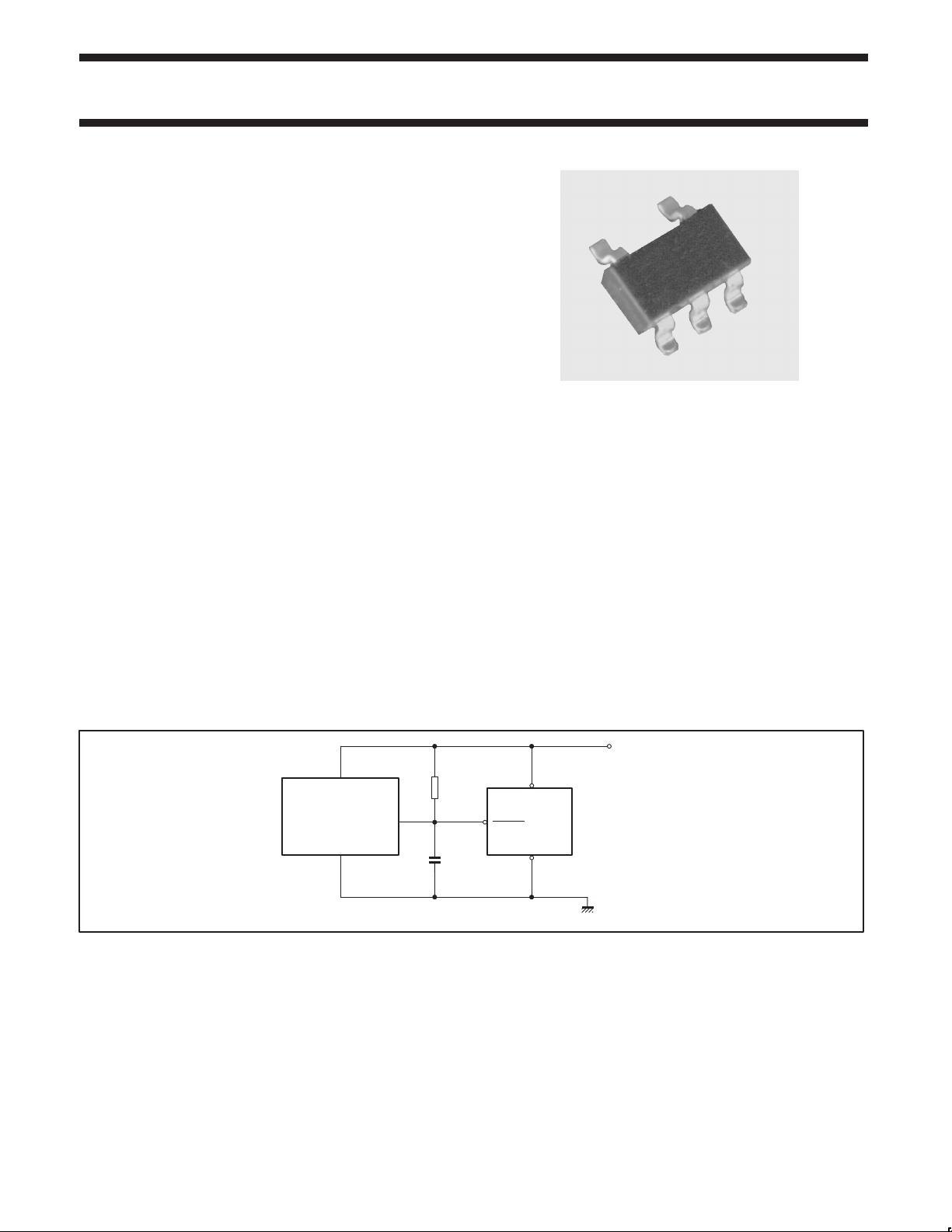
SIMPLIFIED SYSTEM DIAGRAM
down to 0.65 V typ.
CC
V
CC
NE56631-XX
GND
V
OUT
APPLICATIONS
•Reset for microprocessor and logic circuits
•Voltage level detection circuit
•Battery voltage check circuit
•Detection circuit for battery backup
V
CC
RESET
LOGIC SYSTEM
2003 Feb 14
SL01739
Figure 1. Simplified system diagram.
2
Philips Semiconductors Product data
TYPE NUMBER
NE56631-XXActive-LOW system reset
ORDERING INFORMATION
PACKAGE
NAME DESCRIPTION
NE56631-XXD SOT23-5 / SOT25 (SO5) plastic small outline package; 5 leads (see dimensional drawing) –20 to +75 °C
NOTE:
The device has 12 voltage output options, indicated by the XX on
the ‘Type number’.
TEMPERATURE
RANGE
XX
VOLTAGE (Typical)
19 1.9 V
20 2.0 V
27 2.7 V
28 2.8 V
29 2.9 V
30 3.0 V
31 3.1 V
42 4.2 V
43 4.3 V
44 4.4 V
45 4.5 V
46 4.6 V
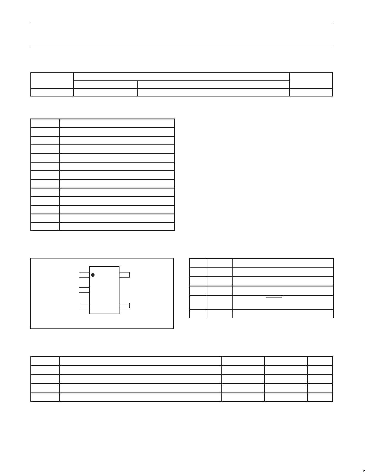
PIN CONFIGURATION
1
NC
2
SUB
34
GND
NE56631-XX
SL01737
5V
CC
V
OUT
PIN DESCRIPTION
PIN SYMBOL DESCRIPTION
1 NC No connection.
2 SUB Substrate. Connect to ground (GND).
3 GND Ground. Negative supply.
4 V
5 V
OUT
CC
Reset output (RESET).
Active-LOW, open collector.
Positive supply voltage
MAXIMUM RATINGS
2003 Feb 14
Figure 2. Pin configuration.
SYMBOL PARAMETER MIN. MAX. UNIT
V
T
T
P
CC
amb
stg
D
Supply voltage –0.3 +10 V
Ambient operating temperature –20 +75 °C
Storage temperature –40 +125 °C
Power dissipation – 150 mW
3
Philips Semiconductors Product data
NE56631-XXActive-LOW system reset
ELECTRICAL CHARACTERISTICS
T
= 25 °C, unless otherwise specified.
amb
SYMBOL PARAMETER CONDITIONS MIN. TYP. MAX. UNIT
V
S
∆V
S
VS/∆T Detection threshold voltage
V
OL
I
LO
I
CCL
I
CCH
t
PLH
t
PHL
V
OPL
I
OL1
I
OL2
Detection threshold voltage RL = 470 Ω; VOL ≤ 0.4 V;
VCC = HIGH-to-LOW
Hysteresis voltage RL = 470 Ω;
0.97 V
V
S
1.03 V
S
S
30 50 100 mV
VCC = LOW-to-HIGH-to-LOW
temperature coefficient
RL = 470 Ω; T
LOW-level output voltage VCC = V
= –20 °C to +75 °C – ±0.01 – %/°C
amb
– 0.05 V; RL = 470 Ω – 0.2 0.4 V
S(min)
Output leakage current VCC = 10 V; VO = VCC – – ±0.1 V
Supply current (LOW Reset) VCC = V
Supply current (HIGH Reset) VCC = V
– 0.05 V; RL = ∞ – 1.0 2.0 µA
S(min)
/ 0.85 V; RL = ∞ – 1.5 2.5 µA
S(typ)
HIGH-to-LOW delay time CL = 100 pF; RL = 4.7 kΩ – 20 60 µs
LOW–to-HIGH delay time CL = 100 pF; RL = 4.7 kΩ – 20 60 µs
Minimum operating threshold voltage RL = 4.7 kΩ; VOL ≤ 0.4 V – 0.65 0.80 V
Output current (LOW Reset) 1 VO = 0.4 V; RL = 0;
VCC = V
S(min)
– 0.05 V
Output current (LOW Reset) 2 VO = 0.4 V; RL = 0;
VCC = V
= –30 °C to +80 °C
T
amb
S(min)
– 0.15 V;
– 30 – mA
– 23 – mA
V
2003 Feb 14
4
 Loading...