

Philips NE5561NB, NE5561D, SE5561FEB, SE5561N Datasheet
Philips Semiconductors Product specification
NE/SE5561Switched-mode power supply control circuit
1
1994 Aug 31 853-0889 13721
DESCRIPTION
The NE5561/SE5561 is a control circuit for use in switched-mode
power supplies. It contains an internal temperature- compensated
supply, PWM, sawtooth oscillator, overcurrent sense latch, and
output stage. The device is intended for low cost SMPS applications
where extensive housekeeping functions are not required.
FEATURES
•Micro-miniature (D) package
•Pulse-width modulator
•Current limiting (cycle-by-cycle)
•Sawtooth generator
•Stabilized power supply
•Double pulse protection
•Internal temperature-compensated reference
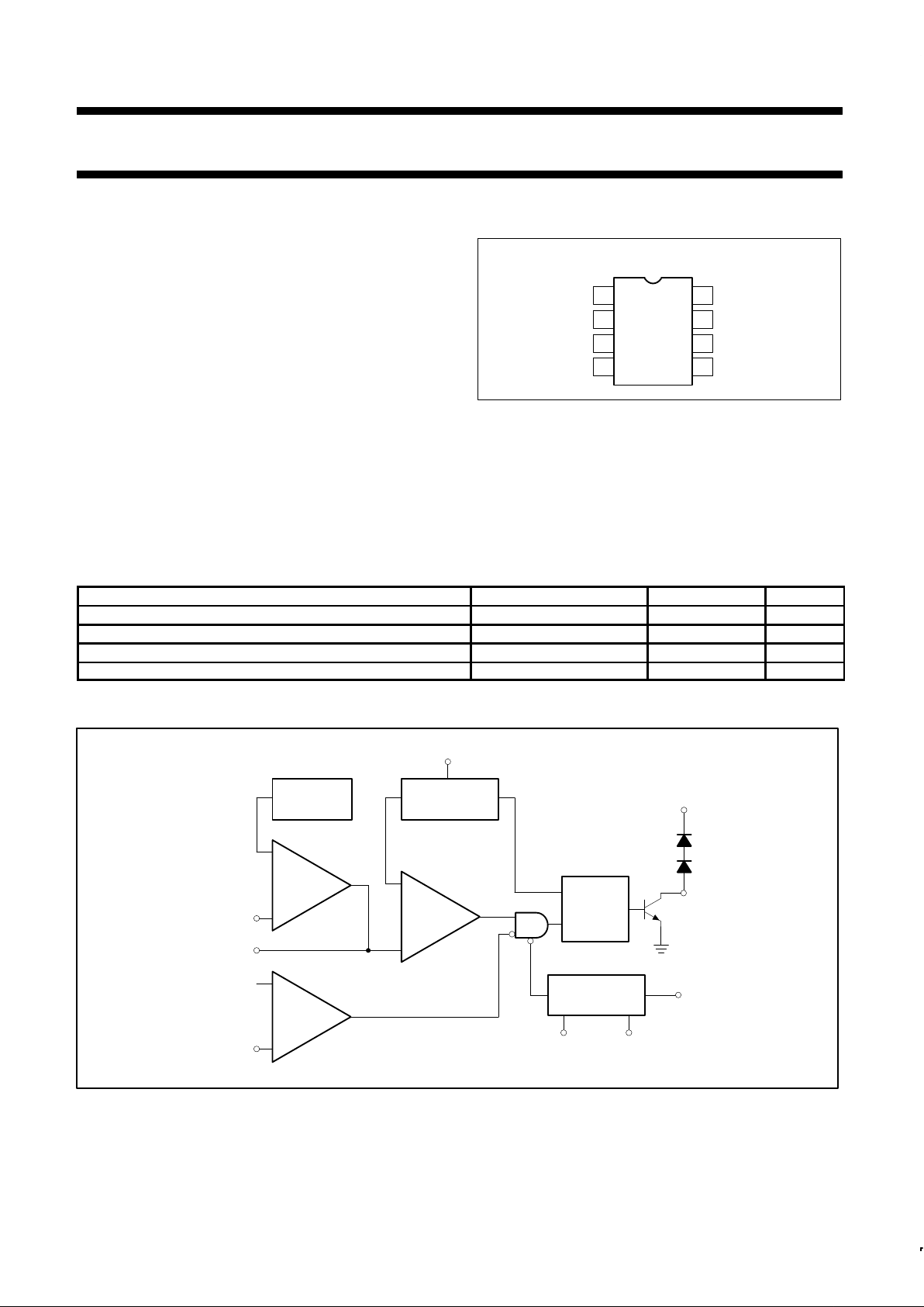
PIN CONFIGURATION
D, FE, N Packages
1
2
3
4 5
6
7
8
V
CC
V
Z
FEEDBACK
GAIN
GND
OUTPUT
CURRENT SENSE
R
T
, C
T
Figure 1. Pin Configuration
APPLICATIONS
•Switched-mode power supplies
•DC motor controller inverter
•DC/DC converter
ORDERING INFORMATION
DESCRIPTION TEMPERATURE RANGE ORDER CODE DWG #
8-Pin Plastic Dual In-Line Package (DIP) 0 to +70°C NE5561N SOT97-1
8-Pin Plastic Dual In-Line Package (DIP) -55 to +125°C SE5561N SOT97-1
8-Pin Ceramic Dual In-Line Package (CERDIP) -55 to +125°C SE5561FE 0580A
8-Pin Small Outline (SO) Package 0 to +70°C NE5561D SOT96-1
BLOCK DIAGRAM
REF
VOLTAGE
SAWTOOTH
GENERATOR
PWM
ERROR
AMP
FEEDBACK
GAIN
0.5V
CURRENT
SENSE
LATCH
S
R
GND
8.2V
OUTPUT
STABILIZED
SUPPLY
1
8
2
+
7
5
3
4
6
–
+
–
V
CC
V
Z
R
T
, C
T
V
CC
SL00385
Figure 2. Block Diagram
Philips Semiconductors Product specification
NE/SE5561Switched-mode power supply control circuit
1994 Aug 31
2
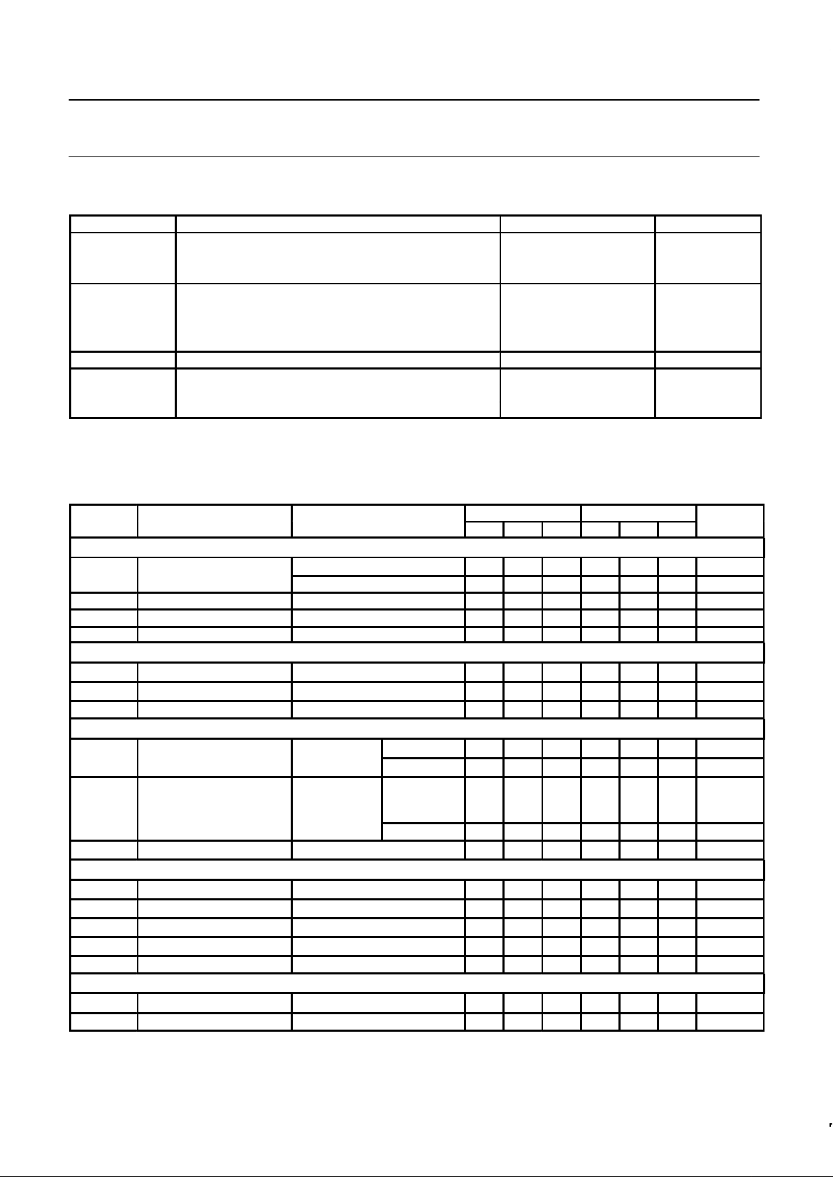
ABSOLUTE MAXIMUM RATINGS
SYMBOL PARAMETER RATING UNIT
V
CC
Supply
1
Voltage-forced mode +18 V
Current-fed mode 30 mA
Output transistor (at 20-30V max)
I
OUT
Output current 40 mA
V
OUT
Output voltage VCC+1.4V V
Output duty cycle 98 %
P
D
Maximum total power dissipation 0.75 W
T
A
Operating temperature range
SE5561 -55 to +125 °C
NE5561 0 to 70 °C
NOTES:
1. See Voltage-Current-fed supply characteristic curve.
DC ELECTRICAL CHARACTERISTICS
VCC=12V, TA=25°C, unless otherwise specified.
SE5561 NE5561
SYMBOL
PARAMETER
TEST CONDITIONS
Min Typ Max Min Typ Max
UNIT
Reference section
V
REF
Internal ref voltage TA=25°C 3.69 3.75 3.84 3.57 3.75 3.96 V
Over temperature 3.65 3.88 3.55 3.98 V
V
Z
Internal zener ref *IL=7mA 7.8 8.2 8.8 7.8 8.2 8.8 V
Temp. coefficient of V
REF
±100 ±100 ppm/°C
Temp. coefficient of V
Z
±200 ±200 ppm/°C
Oscillator section
Frequency range Over temperature 50 100k 50 100k Hz
Initial accuracy RT and CT constant 5 5 %
Duty cycle range fO=20kHz 0 98 0 98 %
Current limiting
I
IN
Input current Pin 6=250mV TA=25°C -2 -10 -2 -10 µA
Over temp. -20 -20 µA
Single pulse inhibit delay
Inhibit delay
time for 20%
overdrive at
I
OUT
=20mA 0.88 1.10 0.88 1.10 µs
I
OUT
=40mA 0.7 0.8 0.7 0.8 µs
Current limit trip level .400 .500 .600 .400 .500 .600 V
Error amplifier
Open-loop gain 60 60 dB
Feedback resistor 10k 10k Ω
BW Small-signal bandwidth 3 3 MHz
V
OH
Output voltage swing 6.2 6.2 V
V
OL
Output voltage swing 0.7 0.7 V
Output stage
I
OUT
Output current Over temperature 20 20 mA
V
CE
Sat IC=20mA, Over temp. 0.4 0.4 V
 Loading...