

Philips NE5560, SE5560 User Manual

Philips Semiconductors Product specification
NE/SE5560Switched-mode power supply control circuit
1
1994 Aug 31 853-0125 13721
DESCRIPTION
The NE/SE5560 is a control circuit for use in switched-mode power
supplies. This single monolithic chip incorporates all the control and
housekeeping (protection) functions required in switched-mode
power supplies, including an internal temperature-compensated
reference source, internal Zener references, sawtooth generator,
pulse-width modulator, output stage and various protection circuits.
FEATURES
•Stabilized power supply
•Temperature-compensated reference source
•Sawtooth generator
•Pulse-width modulator
•Remote on/off switching
•Current limiting
•Low supply voltage protection
•Loop fault protection
•Demagnetization/overvoltage protection
•Maximum duty cycle clamp
•Feed-forward control
•External synchronization
PIN CONFIGURATION
D, F, N Packages
1
2
3
4
5
6
7
8
9
10
11
12
13
14
16
15
V
CC
V
Z
FEEDBACK
GAIN
MODULATOR
DUTY CYCLE CONTROL
R
T
C
T
FEEDFORWARD
OUTPUT (COLL)
OUTPUT (EMIT)
DEMAG: OVERVOLTAGE
GND
CURRENT LIMITING
REMOTE ON/OFF
EXTERNAL SYNC
SL00360
Figure 1. Pin Configuration
ORDERING INFORMATION
DESCRIPTION TEMPERATURE RANGE ORDER CODE DWG #
16-Pin Plastic Dual In-Line Package (DIP) 0 to 70°C NE5560N SOT38-4
16-Pin Plastic Small Outline Large (SOL) Package 0°C to 70°C NE5560D SOT162-1
16-Pin Plastic Dual In-Line Package (DIP) -55°C to 125°C SE5560N SOT38-4
16-Pin Cerdip Dual In-Line Package (CERDIP) -55°C to 125°C SE5560F 0582B
ABSOLUTE MAXIMUM RATINGS
SYMBOL PARAMETER RATING UNIT
Supply
1
V
CC
Voltage-forced mode +18 V
I
CC
Current-fed mode 30 mA
Output transistor (at 20-30V max)
I
OUT
Output current 40 mA
Collector voltage (Pin 15) VCC+1.4V V
Max. emitter voltage (Pin 14) +5 V
T
A
Operating ambient temperature range
SE5560 -55 to +125 °C
NE5560 0 to 70 °C
T
STG
Storage temperature range -65 to +150 °C
NOTES:
1. Does not include current for timing resistors or capacitors.
现货库存、技术资料、百科信息、热点资讯,精彩尽在鼎好!

Philips Semiconductors Product specification
NE/SE5560Switched-mode power supply control circuit
1994 Aug 31
2
BLOCK DIAGRAM
NOTE:
1. See Voltage/Current fed supply characteristic curve.
FEED
FORWARD
EXTERNAL
SYNC INPUT
DEMAGNETIZATION
OVER-VOLTAGE PROTECTION
REFERENCE
VOLTAGE
SAWTOOTH
GENERATOR
FEEDBACK
VOLTAGE
GAIN ADJUST
MODULATOR
INPUT
CUTY CYCLE
CONTROL
CURRENT
LIMITING
+
–
0.48V
0.6V
+
0.6V
0.6V
0.48V
+
–
–
+
+
–
–
+
PULSE WIDTH
MODULATOR
–
+
0.6V
S
R
LATCH
Q
R
S
START
STOP
REMOTE
ON/OFF
STABILIZED
SUPPLY
+ –
0.6V
3
4
5
8
11
10 1 12
2
14
15
13
9
8716
OUTPUTS
C
TRT
V
Z
V
CC
1kΩ
100Ω
OC
1
Q
1
+
–
V
CC
SL00361
Figure 2. Block Diagram

Philips Semiconductors Product specification
NE/SE5560Switched-mode power supply control circuit
1994 Aug 31
3
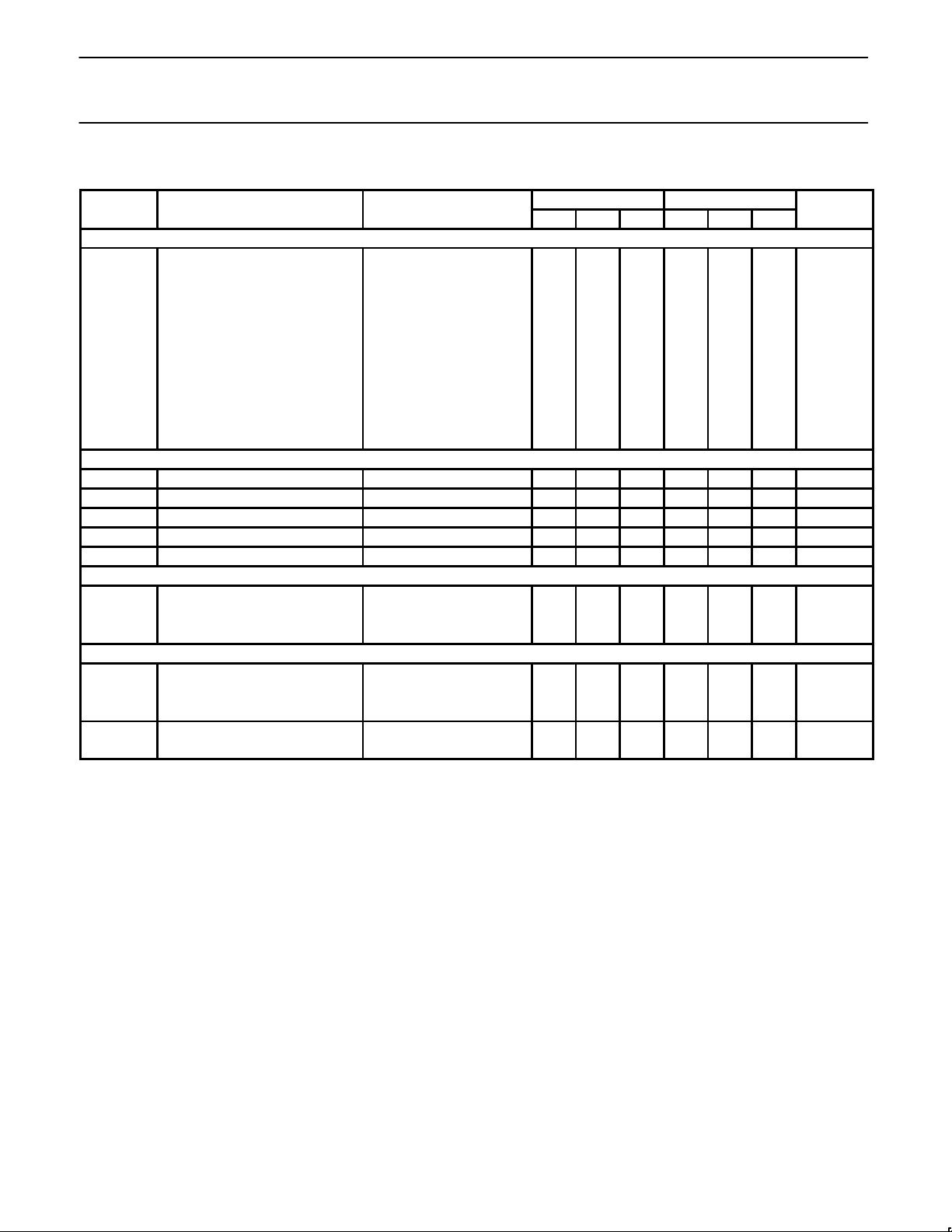
DC ELECTRICAL CHARACTERISTICS
TA=25°C, VCC=12V, unless otherwise specified.
SE5560 NE5560
SYMBOL
PARAMETER
TEST CONDITIONS
Min Typ Max Min Typ Max
UNIT
Reference sections
V
REF
Internal reference voltage 25°C 3.69 3.72 3.81 3.57 3.72 3.95 V
Over temperature 3.65 3.85 3.53 4.00 V
Temperature coefficient of V
REF
-100 -100 ppm/°C
V
Z
Internal Zener reference IL=-7mA 7.8 8.4 8.8 7.8 8.4 8.8 V
Temperature coefficient of V
Z
200 200 ppm/°C
Oscillator section
Frequency range Over temperature 50 100k 50 100k Hz
Initial accuracy oscillator R=5kΩ 5 5 %
Duty cycle range fO=20kHz 0 98 0 98 %
Modulator
Modulation input current
Voltage at Pin 5=2V Over
temperature
0.2 20 0.2 20 µA
Housekeeping function
At 2V
I
IN‘
Pin 6, input current
Over temperature 0.2 20 0.2 20 µA
For 50% max duty cycle
Pin 6, duty cycle limit control
15kHz to 50kHz/41% of V
Z
40 50 60 40 50 60
% of duty
cycle
Pin 1, low supply voltage
protection thresholds
8 9.0 10.5 8 9.0 10.5 V
Pin 3, feedback loop protection trip
threshold
400 600 720 400 600 720 mV
At 2V
Pin 3, pull-up current -7 -15 -35 -7 -15 -35 µA
Pin 13,
demagnetization/over-voltage
protection trip on threshold
Over temperature 470 600 720 470 600 720 mV
At 0.25V
I
IN
Pin 13, input current 25°C -0.6 -10 -0.6 -10 µA
Over temperature -20 -20
Pin 16, feed-forward duty cycle
control
Voltage at Pin 16=2V
Z
30 40 50 30 40 50
% original
duty cycle
At 16V, VCC=18V
*Pin 16, feed-forward input current 25°C 0.2 5 0.2 5 µA
Over temperature 10 10 µA
External synchronization
Pin 9 Off 0 0.8 0 0.8 V
On 2 V
Z
2 V
Z
V
Sink current Voltage at Pin 9=0V, 25°C -65 -100 -65 -125 µA
Over temperature -125 -125 µA
Remote
Pin 10 Off 0 0.8 0 0.8 V
On 2 V
Z
2 V
Z
V
At 0V
Sink current 25°C -85 -100 -85 -125 µA
Over temperature -125 -125 µA
Philips Semiconductors Product specification
NE/SE5560Switched-mode power supply control circuit
1994 Aug 31
4
DC ELECTRICAL CHARACTERISTICS (Continued)
SE5560 NE5560
SYMBOL
PARAMETER
TEST CONDITIONS
Min Typ Max Min Typ Max
UNIT
Current limiting
I
IN
Pin 11 Input current Voltage at
Pin 11=250mV
-2 -20 -2 -20 µA
25°C
Over temperature -40 -40 µA
Single pulse inhibit delay Inhibit delay time for 20%
overdrive at 40mA I
OUT
0.7 0.8 0.7 0.8 µs
OC2 Trip Levels: Shut down, slow start,
low level
0.500 0.600 0.700 0.500 0.600 0.700 V
OC1 Current limit, high level 0.400 0.480 0.560 0.400 0.560 0.500 V
∆OC Low Level in terms of high level,
OC
2
0.750 0.800 0.850 0.750 0.800 0.850 V
Error amplifier
V
OH
Output voltage swing 6.2 9.5 6.2 9.5 V
V
OL
Output voltage swing 0.7 0.7 V
Open-loop gain 54 60 54 60 dB
R
F
Feedback resistor 10k 10k Ω
BW Small-signal bandwidth 3 3 MHz
Output stage
VCE(SAT) IC=40mA 0.5 0.5 V
Output current (Pin 15) 40 40 mA
Max. emitter voltage (Pin 14) 5 6 5 6 V
Supply voltage/current
1
I
CC
Supply current IZ=0, voltage-forced,
VCC=12V, 25°C 10 10 mA
Over temp. 15 15 mA
V
CC
Supply voltage ICC=10mA current-fed 20 23 19 24 V
V
CC
Supply voltage ICC=30mA current-fed 20 30 20 30 V
NOTES:
1. Does not include current for timing resistors or capacitors.
Philips Semiconductors Product specification
NE/SE5560Switched-mode power supply control circuit
1994 Aug 31
5
MAXIMUM PIN VOLTAGES
NE5560
Pin No Function Maximum Voltage
1 V
CC
See Note 1
2 V
Z
Do not force (8.4V)
3 Feedback V
Z
4 Gain
5 Modulator V
Z
6 Duty Cycle Control V
Z
7 R
T
Current force mode
8 C
T
9 External Sync V
Z
10 Remote On/Off V
Z
11 Current Limiting V
CC
12 GND GND
13 Demagnetization/Overvoltage V
CC
14 Output (Emit) V
Z
15 Output (Collector) VCC+2V
BE
16 Feed-forward V
CC
NOTES:
1. When voltage-forced, maximum is 18V; when current-fed, maximum is 30mA. See voltage-/current-fed supply characteristic curve.
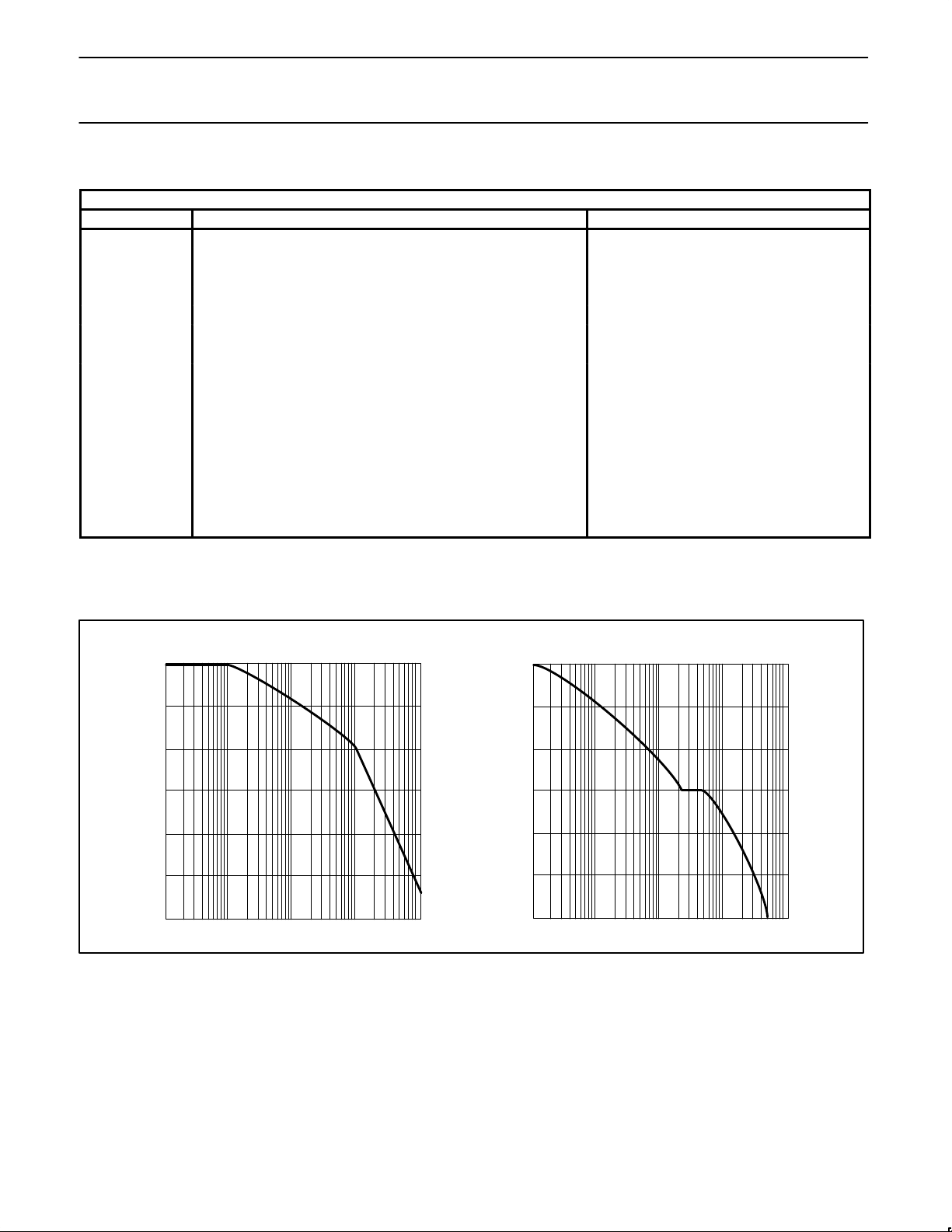
TYPICAL PERFORMANCE CHARACTERISTICS
60
50
40
30
20
10
0
1k 10k 100k 1M 10M
FREQUENCY (Hz)
GAIN (dB)
Open-Loop Gain
0
–30
–60
–90
–120
–150
–180
1k 10k 100k 1M 10M
FREQUENCY (Hz)
PHASE ANGLE (DEG)
Open-Loop Phase
Error Amplifier
SL00362
Figure 3. Typical Performance Characteristics
 Loading...