

Philips FW C220 SI Service Manual

CHANGES IN COURSE OF PRODUCTION
*
In course of production the 3 disc changer module 3CDC-LC has been introduced as an alternative.
Compared to the original used 3CDC-LC-MB there are different servo / motor driver ICs (TDA7073A) used on the CD board.
The new board can be identified by the 12 fig. number 3103 303 34255 printed in the copper pattern.
Note: New chapter 3CDC-LC is enclosed to this Service Information.
*
From production week 0148 to 0152 a different changer module 3CDC99-DS has been used.
This module can be identified by:
- The tray is not
locked and can be opened by simply pulling it out.
- The 12 fig. number printed on the 3CDC99-DS board reads 3103 303 34283.
To enable the use of this 3CDC99-DS version following modifications have been implemented:
Mechanical:
Pos. 107 changed to 8203 306 84031 Cover Tray 3CDC99
Front Board:
7401 changed to 8203 239 35241 TMP87CP71F
Note: This microprocessor will only work in combination with the 3CDC99 Module.
Combi Board:
1509 Flex Foil Socket 15p deleted
1511 Flex Foil Socket 23p (4822 267 10757) added. Pin 20-23 have been removed in order to adapt the socket to the layout
of the Combi Board.
3574 and 3575 changed to 33kΩ (4822 051 20333)
3576 and 3577 changed to 5,6kΩ (4822 051 20562)
Note: The complete chapter 3CDC99-DS is enclosed to this Service Information.
Service Information
SSeerrvviiccee
SSeerrvviiccee
Service
Product Service Group CE Audio
FW-C220
A01-167
©
3139 785 30036
2001-12-13
Already published Service Informations: none

10-1
TABLE OF CONTENTS
Service Hints.....................................................................10-2
Wiring Diagram .................................................................10-4
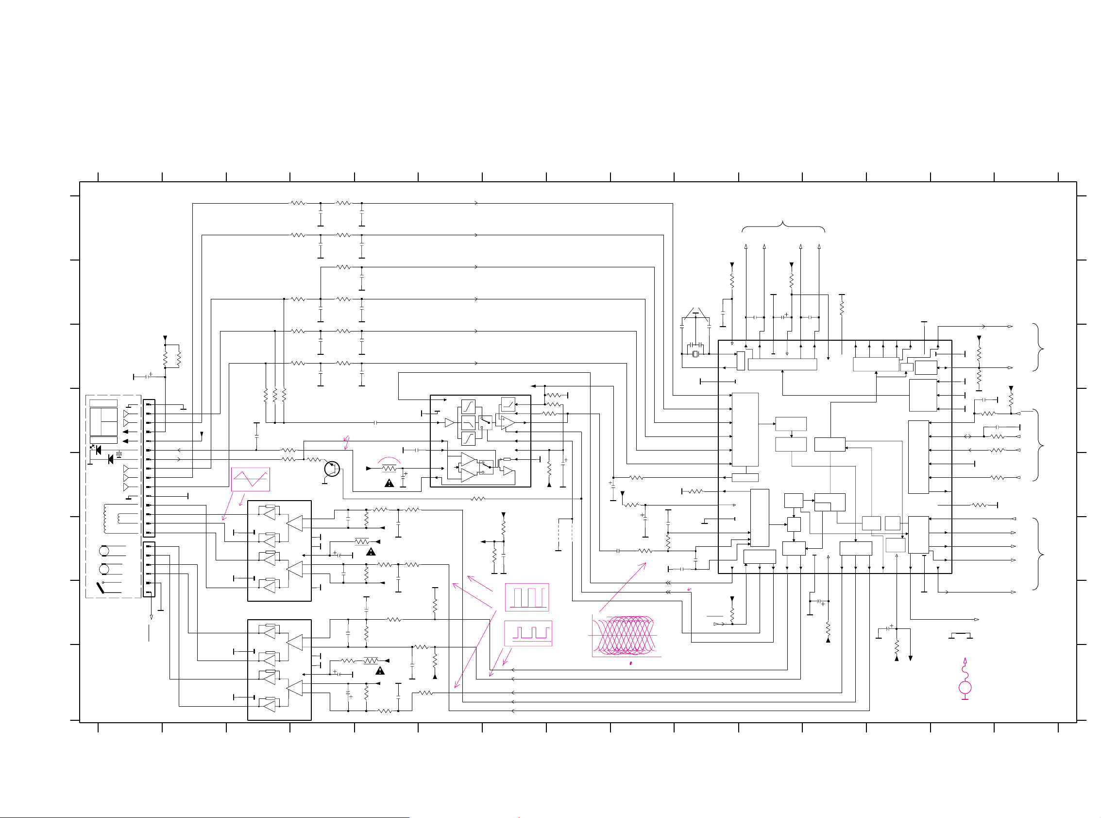
Blockdiagram ....................................................................10-5
Component Layout Main Board ........................................10-6
Circuit Diagram part1........................................................10-7
Component Layout Main Board ........................................10-8
Circuit Diagram part2........................................................10-9
Exploded View ..................................................................10-10
Partslist .............................................................................10-12
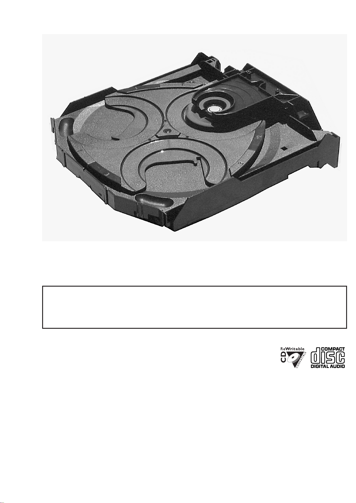
3CDC-LC
(3 Disc Carousel Changer)
Layout stage .5

10-2
The following steps have to be done when replacing the CD mechanism:
1. Disconnect flexfoil cable from the old CD drive
2. Put a paperclip on the flexfoil to short-circuit the contacts (fig.1)
3. Remove the old CD drive
4. Remove paperclip from the flexfoil and connect it to the new drive
5. Position the new CD drive in its studs
6. Remove solder joint from the Laserunit
CHARGED CAPACITORS ON THE SERVO BOARD MAY DAMAGE THE CD DRIVE ELECTRONICS WHEN
CONNECTING A NEW CD MECHANISM. THAT´S WHY, BESIDES THE SAFETY MEASURES LIKE
• SWITCH OFF POWER SUPPLY
• ESD PROTECTION
ADDITIONAL ACTIONS MUST BE TAKEN BY THE REPAIR TECHNICIAN.
fig.1
Attention: The laser diode of this CD drive is protected against ESD by a solder joint which shortcircuits the
laserdiode to ground.
For proper functionality of the CD drive this solder joint must be removed after connection the drive to
the set.
Emergency open
Service hints
In case of a Supply fault, the tray can be opened manually.
1. Remove the top cover of the set to get access to the Changer Module.
2. Turn gearwheel clockwise (as shown in picture below).
CAUTION

10-3
Pos 49 Guiding
Pos 48 Cam
Detail A
Dismantling of Tray
Service hints
1. Open the tray.
2. Release 2x catch as shown in fig. 2 and
Detail A
3. Pull tray out.
fig.2
Assembling of Tray
1. Turn Cam (pos. 48) clockwise to end
position.
2. If necessary - move Guiding (pos. 49) to the
right end position.
3. Insert the Tray.

10-4
Wiring
Disc Motor
Inner switch
Slide Motor
Service Position

10-510-5
DATA
SDA
VCC
1805
D1-D5
D2-D4
7807
7806
7871
7873
TDA7073A
TDA7073A
TDA7073A
HEF4094BT
TTM+
TTM-
MOT2
LD ON
LD
MON
CD R/W
HF IN
V1
D1
D2
D3
D4
R1,R2
MOT1
SLEDGEB-
SLEDGEB+
RADB-
RADB+
FOCB-
FOCB+
+5V
+10V
SHR_CL
STR-OUTP
OE_LATCH
FLEX-FOIL
8001
REGISTER
SHIFT
SERVO - DECODER
CD10
SAA7324 (SAA7325)
Active low pass
Filter
TDA1308
MOTOR
TRAY MOTOR
CARROUSEL
CD DRIVE UP/DOWN SWITCH
1881
1880
TRAY SWITCH
1882
7874
CD POS.1 SWITCH
SL
O2
O0
O1
O7
VDD
+10V
O6
O5
O4
RA
FO
DIODES
PHOTO
D3D2
D5D1
D4
INNER SWITCH
SWITCH INFO
LASER &
MONITOR
DIODE
TURNTABLE
MOTOR
DISC
CD MECHANISM
FOCUS
MOTOR
RADIAL
MOTOR
SLEDGE
MOTOR
MOTOR
TURNTABLE
PHOTODIODE & HF AMPLIFIER - LOADER CONTROL PCB
EN1
DATA
STB
SHR_CL
SICL
SILD
PORE
7875
7801
+3,3V
CD LEFT
78057877
CD RIGHT
Laser Control
&
HF AMPLIFIER
TZA1024 (TZA1025)
55
54
56
38
7
18
20
21
23
15
5
2
3
22
23
18
19
2
4
6
5
9
SWITCH INFO
17
16
15
6
42
40
39
5,17,21,52,57
59
60
64
1
13
+5V
2
+5,6V
8
4
5
7
V4
61
156310
11
6,14
7
14
4
15
2
1
3
16
5
9
11
12
13
5V1
+5V
+3,3V
SCL
SILD
RN
RP
LN
LP
PORE
+
-
+
-
Blockdiagram 3CDC-LC 1999 09 21
Closed if carrousel is in Position 1.
1883
O3
Open if carrousel is in a valid Play-Position.
Closed if the tray is in one endposition.
Open during movement.
Open if the drive is in one endposition.
Closed during movement.
V
t
VDD (pin 16)
EN1 (pin 15)
Power on
Blockdiagram

10-6 10-6
This assembly drawing shows a summary
of all possible versions.
For components used in a specific version
see schematic diagram respectively partslist.
3CDC-LC Mainboard Layout stage .5 10 09 2001
3CDC-LC Mainboard Componentside view
2854 or 3717
This assembly drawing shows a summary
of all possible versions.
For components used in a specific version
see schematic diagram respectively partslist.
3CDC-LC Mainboard Layout stage .5 10 09 2001
3CDC-LC Mainboard Copperside view
Copperside
2800 F4
2801 D4
2802 F4
2803 D4
2805 D4
2806 D4
2807 F4
2808 D4
2810 E4
2811 D4
2815 F3
2816 C3
2818 C4
2822 E3
2823 E3
2824 E3
2825 E4
2829 H3
2830 C4
2831 B3
2832 C4
2833 C4
2834 D4
2835 E2
2836 D4
2840 D1
2841 E2
2842 F2
2844 E2
2850 C3
2852 C2
2853 D2
2854 D2
2855 E4
2856 C3
2857 E2
2859 E3
2862 C4
2863 C4
2864 D2
2865 B3
2867 B4
2869 F4
2872 G2
2877 H1
2878 H1
2879 E2
2882 B3
2887 C4
2891 G2
2892 F3
2893 H1
3700 D2
3705 C2
3706 C1
3707 C2
3708 C2
3709 C3
3711 C2
3712 A3
3713 G3
3714 G2
3715 G2
3716 D2
3717 D2
3718 C2
3727 C3
3728 C3
3730 C3
3731 C2
3732 C2
3733 C2
3734 D2
3735 E3
3736 E3
3740 C4
3741 C4
3742 C4
3743 C3
3744 B4
3746 B3
3750 B4
3751 B4
3770 C3
3771 B5
3772 B5
3780 C3
3781 B3
3782 B5
3800 F4
3801 E4
3802 F4
3803 D4
3804 C3
3805 D4
3806 D4
3807 D4
3808 D4
3809 D2
3811 F4
3814 D4
3819 C3
3820 F4
3821 F4
3822 F4
3823 F3
3824 F3
3825 E3
3826 E3
3827 D4
3828 D2
3831 C2
3832 C3
3833 E4
3834 F4
3837 D2
3838 D2
3839 E2
3840 E3
3841 D2
3842 D2
3843 E2
3844 F2
3845 D2
3846 E2
3847 G2
3848 D3
3849 E2
3850 E1
3853 E4
3854 B5
3855 B5
3856 E4
3857 E4
3858 B5
3859 B5
3860 B4
3861 C4
3862 C4
3863 D2
3864 B4
3866 F3
3867 C4
3868 B3
3869 F4
3870 F4
3871 H1
3872 B3
3873 C3
3874 B3
3875 C2
3876 C2
3877 H1
3878 A5
3879 H3
3880 G3
3881 G2
3882 H2
3883 H3
3884 H3
3885 H3
3886 H2
3887 G2
3888 H1
3889 C2
3890 H2
3891 H2
3892 C2
3893 G2
3894 E4
3895 E3
3897 F2
3898 G2
3899 D5
3900 E2
3901 G3
4800 A5
4801 A4
4802 A4
4803 B2
4804 A5
4805 A5
4806 A5
4807 A5
4808 A5
4809 B5
4810 B4
4811 F2
4812 F2
4813 A4
4814 A4
4815 A4
4816 A4
4817 A3
4818 A3
4819 A3
4820 C4
4821 B2
4822 C5
4823 C5
4824 C5
4825 B3
4826 C3
4827 A4
4828 C2
4829 B2
4830 E2
4831 H4
4832 D2
4833 E3
4834 E4
4835 F3
4836 F4
4837 E3
4838 E3
4839 E3
4840 F3
4841 G2
4842 E3
4843 F3
4844 G3
4845 G4
4846 F4
4847 F4
4848 G4
4849 A4
4876 C5
6871 H1
6872 H2
6873 H2
6874 G3
6875 G2
6876 C5
6877 C4
6878 H2
6879 C2
7801 F3
7804 F2
7805 B4
7812 G3
7850 B5
7851 B5
7860 B5
7861 B5
7873 H2
7874 C2
7875 D4
7876 C2
7877 D3
Componentside
1800 F1
1801 C5
1805 A2
1810 C2
1875 H1
1878 B3
1880 B5
1881 G1
2809 E4
2826 E3
2828 D4
2837 E4
2838 F3
2839 F4
2849 E2
2851 C2
2858 B2
2860 C1
2861 C1
2873 H2
2875 G2
2876 B2
2881 G3
2884 F3
2885 E2
2888 G3
3812 F4
3815 G3
3835 F5
3851 G2
3852 E5
5802 B4
7806 F5
7807 D5
7871 H3
Mapping
10-710-7
SER. DATA
LOOPBACK
INTERF.
KILL
TIMING
BITSTREAM DAC
SER. DATA
INTERFACE
VERSAT.
INTERF.
EBU
INTERF.
CORR.
ERROR
CONTROL
FUNCTION
PRE-
PROCESSING
AUDIO
PROCESSOR
MICROCONTROLLER
INTERFACE
SUBCODE
PROCESSOR
ADDR
SRAM
PEAK
DET.
MOTOR
CONTROL
OUTPUT
STAGES
DIG.
PLL
EFM
DEMOD
VERSATILE
INTERFACE
ADC
VREF GEN.
FRONT
END
VDD
+
-
+
2x
4x
1x
V/I
V/I
Vgap
VDD
+
-
+
(Quartz used)
SLIDE
SLIDE
Signal Processor
F+
L
MON
SLIDE
D
D2
D5
D4
D
E
F
G
H
T+
on
#
1 2 3 4 5 6 7 8 9 101112131415
123456
D3 (CD10)
D2 (CD10)
DISC
R2 (CD10)
D2
D
3863 = 33R
D1
8 9 10 11 12 13 14 15
A
B
C
D
E
F
G
H
A
+
HF-Amplifier
Motor Driver
+
CD Drive
D4 (CD10)
VREF
LD
GND
D3
+
GND
+
7
D2
F-
D
PIN50
B
C
3CDC-LC-mainboard
DOBM
dig. out circuitry
part 1
D3
_
#.... for provision only
VCC
/ SAA7325
D1 (CD10)
D5
#
_
TRACK
FOCUS
_
for Coax out versions
for basic version
only for digital out versions
/ TZA1025
FOCUS
D
part 2
TRACK
FOCUS
for digital out version:
D4
+
TRACK
Laser power control
from 1801
D
DISC
+
DISC
_
D
to 7877
D
R1 (CD10)
Servo driver
VAM2201
D4
T-
D1
D3
INNERSW.
D5
_
_
D1
#
to
33p
2833
3735
+3.3V
680K
3736
680K
10u
2838
120R
3867
33K
3827
3897
100R
100K
3839
2810
180p
3728
4K7
+3.3V
2849 4u7
2834
33p
2811
220p
MP893
82K
3849
2857
10n
3826
22K
+10V
27p
2856
2824
22n
3850
4K7
3807
10K
3815
4R7
3832
4u7
2888
+3.3V
10K
2816
1n5
3824 1K
4K7
3727
3806
10K
3862
120R
100n
2887
+3servo
+3.3V
3853
470R
3805
10K
33
VSSD1
50
VSSD2
58
VSSD3
35
WCLI
28
WCLK
3852
2R2
31
TEST2
44
TEST3
63
V1
34
V2|V3
61V462
V5
5
VDDA1
17
VDDA2
52
VDDD1P
57
VDDD2C
20
VNEG21VPOS
7
VRIN
4
VSSA1
14
VSSA2
RESETn
22RN23
RP
48
SBSY
40
SCL
37
SCLI
29
SCLK
39
SDA
36
SDI
24
SELPLL
47
SFSY
42
SILD
SL
56
43
STATUS
46
SUB
25
TEST1
1
HFREF
6
IREF
3
ISLICE
32
KILL
64
LDON
18LN19
LP
59
MOTO160MOTO2
12
R1
13
R2
54
RA
RAB
41
45
RCK
38
53
CFLG
49
CL11|4
26
CL16
16
CRIN
15
CROUT
8
D1
9
D2
10
D3
11
D4
27
DATA
51
EF
30
55
FO
2
HFIN
3844
+10V
SAA7324
7877
47u
4K7
10K
3803
2828
4K73820
3812
2R2
270p
3892
470R
2841
3800
56K
MP844
2805
220p
22K
3834
+3.3V
10K
3804
10
11
12
13
14
15
2
3
4
5
6
7
8
9
1800
1
270p
2844
8
11
15
14
10
2
1
6
7
16
13
9
12
5
3
4
47K
TDA7073A 7807
470R3873
3845
+3.3V
47n
2879
3828
22K
2806
220p
+3.3V
10K
3801
VCCL
11
CDRW
3
CFIL
8
CMFB
5
DIN
12
EQSEL
6
GND
1
LD
4
MON
7
PWRON
10
RFEQO
9
RFFB
14
RGADJ
13
VCC2
2
4R7
7801
TZA1024
3869
470R
3889
2808
220p
EBUGND
3856
68R
180p
2802
22K
3833
2839
47u
4u72884
+3servo
4K73821
+3.3V
3843
2826
47u
2859
10n
33K
47K
3842
1n5
2818
1K
3823
6K8
3847
47n
2825
220p
2803
3709
4K7
3841
1R
2800
180p
3825
1K
330p
2807
1K3838
3840
2842
2n2
100K
15K3870
100n
10K
2840
3808
4811
10K
3866
4812
+5V
3811
18K
2891
1n5
220p
2801
2823
56p
3822
2851
220u
2809
2K7
47u
2837
0u47
470p
2855
2885
4u7
+3.3V
68R
3857
4n72892
+3servo
3802
16
13
9
12
5
3
4
8
11
15
56K
7806TDA7073A
14
10
2
1
6
7
1
2
3
4
5
6
1801
PH-S
1810
TF01
2850
1n
3895
15R
+5V
470R
3819
3846
1K
3837
33K
220n
2815
47n
2869
3848
100K
2835
2822
47n
2n2
100R
3R3
3835
3863
M1
3894
100R
VrefCD10
HFIN
KILL_R
Vref
Innersw
Vref
VrefCD10
FO
Vref
DOBM
CL11
KILL_L
LPLN
RAM2
RN
RCK
SBSY
RP
SFSY
SL
SUB
Innersw
SILD
SICL
SDA
PORE
HFOUT
Vref
3CDC-LC Part1 20001127
To 7876 on part 2
(CD-Text IC)
To 1805 on part 2
(µP-Interface)
To 3770,3780 on part 2
(Mute)
To 7805 on part 2
3900
10K
BC847B
7804
82K
3901
1800 D1
1801 G1
1810 C10
2800 C4
2801 C5
2802 C4
2803 C5
2805 B5
2806 B5
2807 A4
2808 A5
2809 H4
2810 A4
2811 A5
2815 D5
2816 B12
2818 B11
2822 F9
2823 F10
2824 F10
2825 F9
2826 G12
2828 G13
2833 C10
2834 C10
2835 F7
2837 H4
2838 E8
2839 F4
2840 G4
2841 F5
2842 F5
2844 F5
2849 C1
2850 D14
2851 B11
2855 B4
2856 D15
2857 H5
2859 G5
2869 D3
2879 H5
2884 E8
2885 F9
2887 B10
2888 E5
2891 F4
2892 D5
3709 C14
3727 B12
3728 E14
3735 G6
3736 H6
3800 C4
3801 C4
3802 C4
3803 C4
3804 C14
3805 B4
3806 B4
3807 A4
3808 A4
3811 B4
3812 H4
3815 E5
3819 D14
3820 D3
3821 D3
3822 D3
3823 D8
3824 D8
3825 F9
3826 F9
3827 E10
3828 G10
3832 D15
3833 A4
3834 A4
3835 F5
3837 F7
3838 F7
3839 H6
3840 G5
3841 G5
3842 E5
3843 E5
3844 F5
3845 F5
3846 F5
3847 F5
3848 H6
3849 H5
3850 H5
3852 H5
3853 E9
3856 C1
3857 C2
3862 B10
3863 H13
3866 D8
3867 B11
3869 D3
3870 E3
3873 D14
3889 D15
3892 E15
3894 E9
3895 G12
3897 E7
3900 E6
3901 E4
4811 F8
4812 F8
7801 E7
7804 E4
7806 G4
7807 H4
7877 D12
0V
for CD TEXT only
4.7V
during Focus search
1V
1.6V
0V
3.2V
3.4V
0.9V
1.7V
1.7V
3.0V
for CD_DA : 0V
3V
3V
1.6V
1.6V
3.2V
0.8V
5.1V
1.6V
4.8V
0.3V
1.6V
0V
->Laser damaged !
3.2V
1.6V
0V
1.7V
1.6V
1.6V
0.3V
0V
3V
1.6V
3V
1.6V
0.2V
0V
1.9V
2.9V
ESD sensitive lines!
2.9V
5V
1.6V
EYE-PATTERN
1.6V
4.7V
3.2V
0.8V
2.1V
3.2V
1.6V
10V
1.6V
11.3 MHz
0V
U >400mV
4.7V
1.6V
1.6V
1.6V
4.6V
5V
1.6V
1.6V
10V
5V
for CD_RW : 3V
TB = 0.5us/div
1.7V
3V
1.6V
1.6V
4.9V
0V
1.6V
800mVpp
EVM
V
...DC voltages measured
in Play mode
for CD_DA : 0V
for CD_RW : 0,7V
10-8 10-8
This assembly drawing shows a summary
of all possible versions.
For components used in a specific version
see schematic diagram respectively partslist.
3CDC-LC Mainboard Layout stage .5 10 09 2001
3CDC-LC Mainboard Componentside view
2854 or 3717
This assembly drawing shows a summary
of all possible versions.
For components used in a specific version
see schematic diagram respectively partslist.
3CDC-LC Mainboard Layout stage .5 10 09 2001
3CDC-LC Mainboard Copperside view
Copperside
2800 F4
2801 D4
2802 F4
2803 D4
2805 D4
2806 D4
2807 F4
2808 D4
2810 E4
2811 D4
2815 F3
2816 C3
2818 C4
2822 E3
2823 E3
2824 E3
2825 E4
2829 H3
2830 C4
2831 B3
2832 C4
2833 C4
2834 D4
2835 E2
2836 D4
2840 D1
2841 E2
2842 F2
2844 E2
2850 C3
2852 C2
2853 D2
2854 D2
2855 E4
2856 C3
2857 E2
2859 E3
2862 C4
2863 C4
2864 D2
2865 B3
2867 B4
2869 F4
2872 G2
2877 H1
2878 H1
2879 E2
2882 B3
2887 C4
2891 G2
2892 F3
2893 H1
3700 D2
3705 C2
3706 C1
3707 C2
3708 C2
3709 C3
3711 C2
3712 A3
3713 G3
3714 G2
3715 G2
3716 D2
3717 D2
3718 C2
3727 C3
3728 C3
3730 C3
3731 C2
3732 C2
3733 C2
3734 D2
3735 E3
3736 E3
3740 C4
3741 C4
3742 C4
3743 C3
3744 B4
3746 B3
3750 B4
3751 B4
3770 C3
3771 B5
3772 B5
3780 C3
3781 B3
3782 B5
3800 F4
3801 E4
3802 F4
3803 D4
3804 C3
3805 D4
3806 D4
3807 D4
3808 D4
3809 D2
3811 F4
3814 D4
3819 C3
3820 F4
3821 F4
3822 F4
3823 F3
3824 F3
3825 E3
3826 E3
3827 D4
3828 D2
3831 C2
3832 C3
3833 E4
3834 F4
3837 D2
3838 D2
3839 E2
3840 E3
3841 D2
3842 D2
3843 E2
3844 F2
3845 D2
3846 E2
3847 G2
3848 D3
3849 E2
3850 E1
3853 E4
3854 B5
3855 B5
3856 E4
3857 E4
3858 B5
3859 B5
3860 B4
3861 C4
3862 C4
3863 D2
3864 B4
3866 F3
3867 C4
3868 B3
3869 F4
3870 F4
3871 H1
3872 B3
3873 C3
3874 B3
3875 C2
3876 C2
3877 H1
3878 A5
3879 H3
3880 G3
3881 G2
3882 H2
3883 H3
3884 H3
3885 H3
3886 H2
3887 G2
3888 H1
3889 C2
3890 H2
3891 H2
3892 C2
3893 G2
3894 E4
3895 E3
3897 F2
3898 G2
3899 D5
3900 E2
3901 G3
4800 A5
4801 A4
4802 A4
4803 B2
4804 A5
4805 A5
4806 A5
4807 A5
4808 A5
4809 B5
4810 B4
4811 F2
4812 F2
4813 A4
4814 A4
4815 A4
4816 A4
4817 A3
4818 A3
4819 A3
4820 C4
4821 B2
4822 C5
4823 C5
4824 C5
4825 B3
4826 C3
4827 A4
4828 C2
4829 B2
4830 E2
4831 H4
4832 D2
4833 E3
4834 E4
4835 F3
4836 F4
4837 E3
4838 E3
4839 E3
4840 F3
4841 G2
4842 E3
4843 F3
4844 G3
4845 G4
4846 F4
4847 F4
4848 G4
4849 A4
4876 C5
6871 H1
6872 H2
6873 H2
6874 G3
6875 G2
6876 C5
6877 C4
6878 H2
6879 C2
7801 F3
7804 F2
7805 B4
7812 G3
7850 B5
7851 B5
7860 B5
7861 B5
7873 H2
7874 C2
7875 D4
7876 C2
7877 D3
Componentside
1800 F1
1801 C5
1805 A2
1810 C2
1875 H1
1878 B3
1880 B5
1881 G1
2809 E4
2826 E3
2828 D4
2837 E4
2838 F3
2839 F4
2849 E2
2851 C2
2858 B2
2860 C1
2861 C1
2873 H2
2875 G2
2876 B2
2881 G3
2884 F3
2885 E2
2888 G3
3812 F4
3815 G3
3835 F5
3851 G2
3852 E5
5802 B4
7806 F5
7807 D5
7871 H3
Mapping
 Loading...