

Page 1
Technical specification ......................................................1-1
Features ............................................................................1-1
Accessories .......................................................................1-1
Instruction For Use .....................................................1-2..1-6
Safety & Warnings.............................................................1-7
Service hints
Repair positions ............................................................2-1
Dismantling CD-door.....................................................2-1
Handling chip components............................................2-2
Service tools..................................................................2-2
Pin descriptions of ICs................................................3-1..3-7
Service Test Program........................................................3-8
Blockdiagram.....................................................................3-9
Circuit diagrams
Control/ESP part............................................................4-1
Audio part......................................................................4-2
CD Drive part.................................................................4-3
Power Supply part .........................................................4-4
Layout diagrams
Copper side view ...........................................................4-5
Component side view ....................................................4-6
Exploded view ...................................................................5-1
Mechanical partslist ...........................................................5-1
Electrical partslist .......................................................6-1..6-3
© 3140 785 32610
Published by LX 0330 Service Audio Printed in The Netherlands Subject to modification
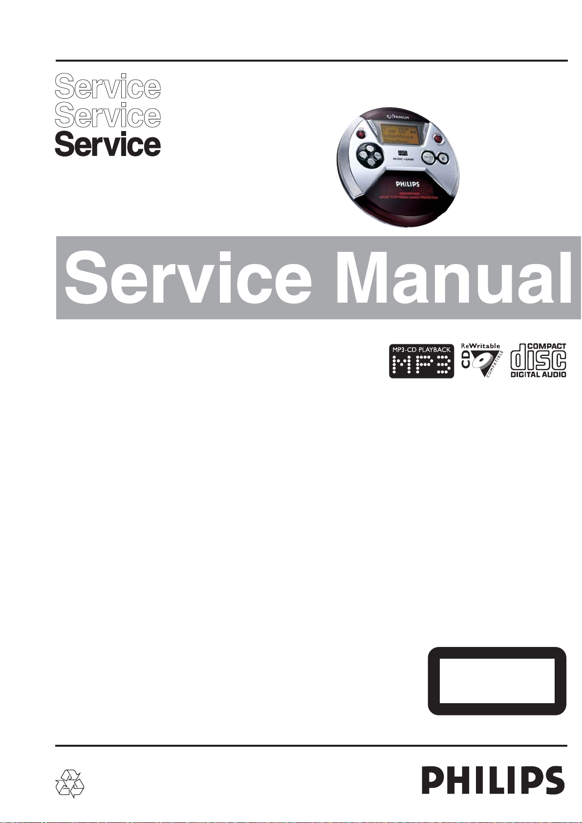
Portable compact disc player
TABLE OF CONTENTS
©
Copyright 2001 Philips Consumer Electronics B.V. Eindhoven, The Netherlands
All rights reserved. No part of this publication may be reproduced, stored in a retrieval
system or transmitted, in any form or by any means, electronic, mechanical, photocopying,
or otherwise without the prior permission of Philips.
all versions
EXP521
CLASS 1
LASER PRODUCT
Page 2
1-1
TECHNICAL SPECIFICATION
General
Dimensions (Wx H x D) : 137.5 x 30x 137.5mm
Weight without batteries : 220g
Shock resistance
+X/-X direction : ≥2.5g
+Y/-Y direction : ≥2.5g
+Z/-Z direction : ≥2.0g
Power supply modes
Battery lifetime
Battery level detection
Current consumption
Headphone out
Output power (THD=10%)
/17 version only : 6mW (+1/-3dB)
all other versions : 3mW (+1/-3dB)
Frequency response (1mW) : 100Hz-20kHz within 6dB
S/N ratio CD (unwght) : ≥78dB (80dB typ.)
S/N ratio CD (unw.),incl.muting : 100dB
S/N ratio CD (A-wght) : ≥80dB (82dB typ.)
S/N ratio CD (A-wght),incl.muting : 100dB
THD+N (1kHz, 1mW) : ≤1.5% (1.0% typ.)
Crosstalk (1kHz) : ≤-24dB (-44dB typ.)
Channel unbalance (-40dB) : ≤5dB
Volume attenuation (1kHz) : >60dB
Dynamic Bass Boost DBB
Measurement setup CD
Use Audio Signal disc SBC429 4822 397 30184
Battery empty
Difference btw.level 1 and battey empty
Difference btw.level 2 and battey empty
Difference btw.level 3 and battey empty
1.8V
+100/-50mV
0.3V
± 100mV
0.6V ± 100mV
0.9V ± 100mV
ACCESSORIES
++0dB 0dB
± 2dB 2dB
0dB dB
± 2dB 2dB
0dB dB
± 2dB 2dB
+5dB dB
± 2dB 2dB
+0dB dB
± 2dB 2dB
+8dB dB
± 2dB 2dB
DBB 1
DBB 2
DC
MP3
MP3
≥
10 h
(14h typ.)
≥
24 h
(28h typ.)
≥
7 h
(10h typ.)
≥
6 h
(8h typ.)
seirettabAlkaline
AAA)x(2
≥
2 h
(4h typ.)
≥
8 h
(10h typ.)
≥
2 h
(3h typ.)
≥
1 h
(2h typ.)
seirettabRechargable
)(AY3363
≥
2 h
(3h typ.)
≥
5 h
(6h typ.)
≥
1 h
(2h typ.)
≥
1 h
(2h typ.)
ESP=on
ESP=on ESP=off
FEATURES
EDOMYLPPUS
tekcosNI-CDV6-3.9
seirettabyramirP
EPYTYRETTAB
AA)x(2
seirettabAlkaline
seirettabRechargable
ESP=off
DC
egnaregatloV
DC
V2.3-9.1
V2.3-9.1
EGATSBBD
zH63 zH1k zHk01
esnopserycneuqerF
L
R
Low pass filterDUT S/N and distortion meter
22kHz
13th order
i.e. Sound Technology ST1700Bi.e. 4822 395 30204
Level meter
i.e. Sennheiser UPM550
with FF-filter
SERUTAEF
ELBATROP-DCFO
/MP3
WM/MFRENUT
125EXP
)snoisrevlla(
-/-
LEVELNOITCETED seirettabyramirP
on=PSE
300mA
480mA
)V5.4(YLPPUSNI-CD )V52.2(YLPPUS.TTAB
300mA
480mA
CD
MP3
off=PSE
CD MP3
onP=SE
250mA 250mA 250mA
n/a n/a n/a n/a
480mA 480mA 480mA 480mA
offP=SE
on=PSE
Play
Charge
Jump
Stand-by
NOITAREPO
CD
EDOM
CD MP3
onP=SE
offP=SE
220mA
220mA 220mA 220mA 250mA
300mA
300mA
480mA
480mA
60mA 60mA 60mA 60mA 1mA 1mA 1mA 1mA
MP3
YTILIBITAPMOCELBATIRWER-DC
N CDDA / MP3OITCETORPPIKSCINORTCELE
EZISMARDPSE
NOITCNUFEMUSER/DLOH
SEGATSBBD
KCABDEEFCITSUOCA
YROMEMMARGORP
HMiN/dCiNNOITCNUFEGRAHCER
DERAPERPLORTNOCETOMERDROC
●
s / 420s168
● / ●
2
-
/-
●
tibM8
05
●
off=PSE
00/0613YA rotpadACD/CA
3140 118 31051
SEIROSSECCA
ELBATROP DCROF
-TARGET
C00/ 10/
X
20/0613YA rotpadACD/CA
3140 118 31122
05/0613YA rotpadACD/CA
3140 118 30761
10A/0613YA rotpadACD/CA
3140 118 31171
SBC HE570
9082 100 01724
SBC HS383
7s7/
7s7/
e
noh
pdaeHoeretS
pdaeHoeretS
X
enoh
9082 100 01821
AY 3778
Remote Control
3140 118 51491
AY 3363
Rechargeable battery
3103 308 84721
XXX XXX
XXX X
EXP521
10/
X
X
XX
/05Z 07/
/17
X
X
XX
Page 3
1-2
W
y
INSTRUCTION FOR USE
TROUBLESHOOTING
ARNING: Under no circumstances should you try to repair the set
ourself as this will invalidate the warranty.
If a fault occurs, first check the points listed, before taking the set for
repair. If you are unable to solve a problem by following these hints,
consult your dealer or service center.
No power, playback does not start
–Insert the batteries correctly.
– Replace the batteries.
– Connect the power adapter securely.
Hold indication and/ or no reaction to controls
1
7
8
9
0
!
@
#
6
5
4
3
2
1
– Deactivate HOLD.
–Disconnect the set from the power supply or take out the batteries
$
for a few seconds.
No sound or bad sound quality
– Press 2; to resume playback.
– Adjust the volume.
– Check and clean the connections.
%
– Keep this set away from active mobile phones or strong magnetic
(
*
&
fields.
pls insert CD or No audio file indication
+
+
–Insert a disc, label upwards.
–Clean or replace the disc.
–Wait until the steamed up lens has cleared.
–Make sure you have inserted an audio disc or an MP3-CD.
^
Music file is not played
–Make sure that the file names of the MP3 files end with .mp3
Missing directories on MP3-CD
–Make sure the total number of files and albums on your MP3-CD
does not exceed 350.
– Only albums with MP3 files are shown.
The disc skips tracks
–Clean or replace the disc.
–Make sure repeat, repeat album, shuffle or prog are not
selected.
Music skips or popping sound when playing an MP3 file
–Play the music file on your computer. If the problem persists,
encode the audio track again and make a new CD-ROM.
Music is interrupted and Oops indication
– Switch ESP on.
In-car use: No power, playback does not start
–Clean the cigarette lighter jack.
– Switch on the ignition of your car.
In-car use: No sound or bad sound quality
–Insert the adapter cassette correctly.
– Change the autoreverse direction of your car cassette player.
– Let the set adjust to the temperature in the car.
QUICK START MISE EN SERVICE RAPIDE INCIO RAPIDO
Page 4

1-3
INSTRUCTION FOR USE
English
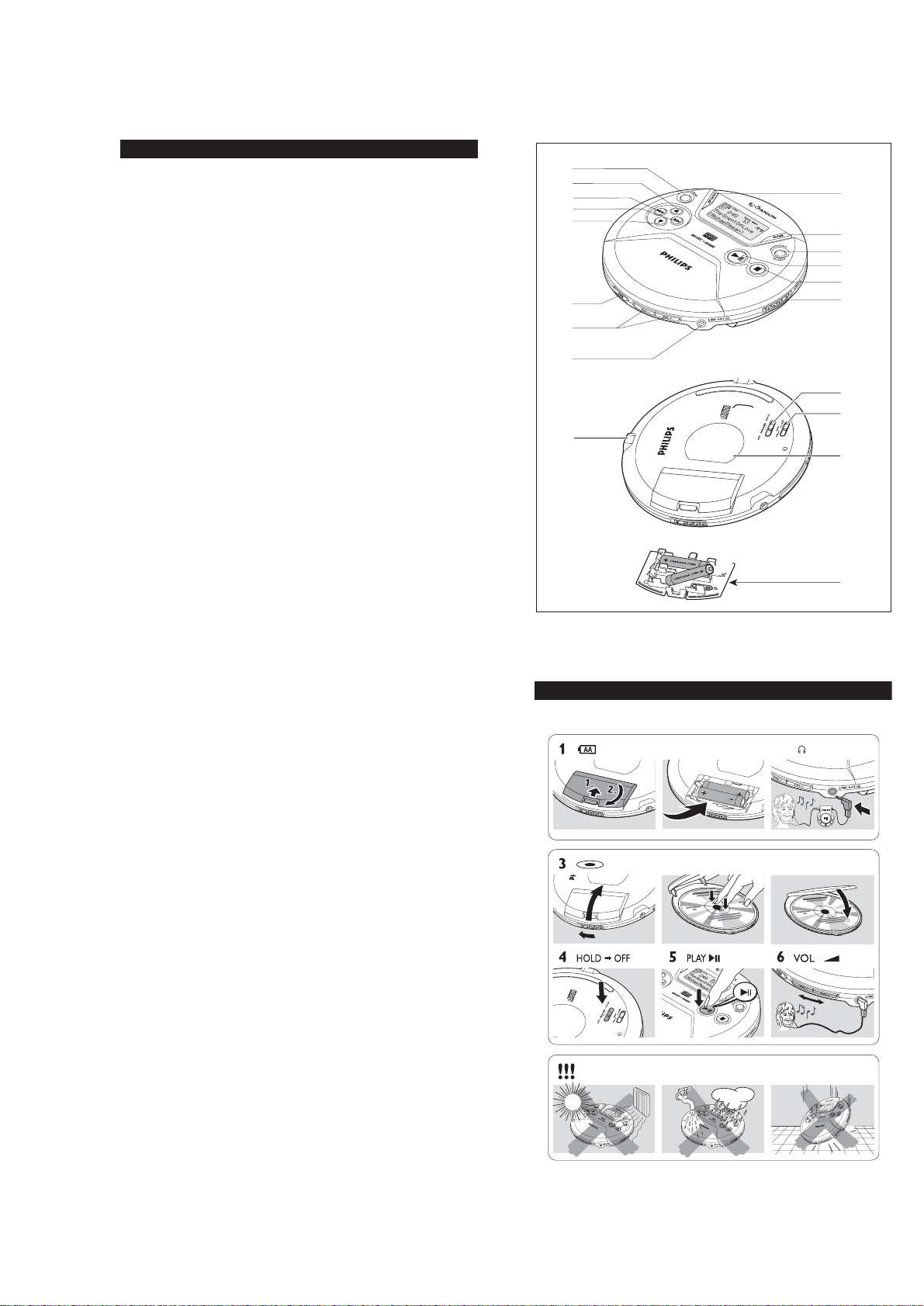
CONTROLS (see figure
1)
CONTROLS
1 OPEN 2 . . . . . . opens the CD lid
2 9 . . . . . . . . . . . . stops playback and switches the set off
3 2; . . . . . . . . . . . switches the set on, starts playback and
interrupts playback
4 PROGRAM/ . . . MUSIC mode: programs tracks and lets you
SHOOT/ review the program
SELECT GAME mode: confirms selection of a game,
setting, etc./ shoot to score
5 MODE . . . . . . . . selects music playback options such as random
order and repeat
6 DISPLAY. . . . . . selects the track and album information for
MP3-CDs
7 GAME . . . . . . . . selects game mode on/ off
8 3. . . . . . . . . . . . MP3-CD only: selects the next album or fast
skips tracks forward
GAME mode: move up
§
9 . . . . . . . . . . . MUSIC mode: skips backward and searches
backward
GAME mode: move left
. . . . . . . . . . . MUSIC mode: skips forward and searches
0 §
forward
GAME mode: move right
! 4. . . . . . . . . . . . MP3-CD only: selects the previous album or fast
skips tracks backward
. . . . . . . . . . . . . GAME mode: move down
BATTERIES
(supplied or optionally available)
You can use the following batteries with this CD-player:
•alkaline batteries type AAA (LR03, UM4) or AA (LR6, UM3)
preferably Philips).
Notes:
–
Old and new or different types of batteries should not be combined.
– Remove batteries if they are empty or if the player is
not going to be used for a long time.
Inserting AAA (LR03, UM4) or AY3363
batteries
1 Open the AAA battery door.
AAA (LR03, UM4)
2 Insert AAA batteries as shown onto the back
of the door.
3 Replace the battery-loaded AAA door back
onto the set.
Inserting AA (LR6, UM3) batteries
To increase playback time, insert AA batteries
AA (LR6, UM3)
into the battery compartment and use the AA marked battery door.
• Open the battery compartment and insert either 2 normal or alkaline
batteries.
Indication of empty batteries
• Replace the batteries or connect the power adapter as soon as
A blinks and Replace batteries.
Remove batteries if they are empty or if the set will not be used for a
long time.
@ DBB . . . . . . . selects the bass adjustment
# VOL + / - . . . . . . adjusts the volume
$ LINE OUT/p . . 3.5 mm line out to connect
– the headphones
– the remote control
– this set to the audio input of your stereo
equipment
% 4.5V DC.
. . . . . . to connect the external power supply
^ AAA battery door
& type plate
* ESP . . . . . . . . . . Electronic Skip Protection prevents music
interruptions caused by shocks
( OFF• . . . . . . . . . OFF switches RESUME and HOLD off
RESUME• RESUME stores the last position played
HOLD HOLD locks all buttons
Supplied Accessories:
1 x headphones, HE570 or HS383
x rechargeable batteries, AY3363
2
1 x remote control, AY3778
1 x headphone jack adapter (for some versions only)
x AC/ DC adapter, AY3160
1
(supplied
or optionally available)
CAUTION
Use of controls or adjustments or performance of procedures
other than herein may result in hazardous radiation exposure or
unsafe operation.
other
Batteries contain chemical substances,so they should be
disposed of properly.
POWER ADAPTER
(supplied or optionally available)
Use only the AY3160 adapter (4.5V/ 400mA direct current, positive pole to
the center pin). Any other product may damage the
player.
1 Make sure the local voltage corresponds to the
power adapter’s voltage.
2 Connect the power adapter to the 4.5V DC jack
of the player and to the wall outlet.
Note: Always disconnect the adapter when you are not using it.
ENVIRONMENTAL INFORMATION
• All redundant packing material has been omitted. We have done our
utmost to make the packaging easily separable into two materials:
cardboard (box) and polyethylene (bags, protective foam sheet).
•Your set consists of materials which can be recycled if disassembled by
a specialized company. Please observe the local regulations regarding
the disposal of packing materials, dead batteries and old equipment.
This set complies with the radio interference requirements
of the European Community.
Page 5
1-4
INSTRUCTION FOR USE
REMOTE CONTROL AY3778
(supplied or optionally available)
Use the AY3778 cord remote control. The
buttons on the remote control have the
same functions as the corresponding
buttons on the set.
1 Press 9 twice to switch off the set.
2 Firmly connect the remote control to
LINE OUT/ p on the set.
3 Adjust the volume on the CD player and remote control.
HEADPHONES
• Connect the supplied headphones to the
LINEOUT/ p jack of the player.
Note:
– LINE OUT/ p can also be used for connecting
this set to your HiFi system.To adjust the sound
and volume, use the controls on the connected
audio equipment and on the CD player.
IMPORTANT!
Hearing safety: listen at a moderate volume. using headphones at high volume can
impair your hearing.
Traffic safety: do not use headphones while driving or cycling as you may cause an
accident.
IN-CAR USE ACCESSORIES
(connections supplied or optionally available)
Only use the AY3545 or AY3548 car voltage
converter (4.5V DC, positive pole to the center
pin) and the AY3501 car cassette adapter. Any
other product may damage the set.
1 Put the set on a horizontal, vibration-free
and stable surface. Make sure it is in a
safe place, where the set is neither a
danger nor an obstacle to the driver and
the passengers.
2 Plug the voltage converter into the cigarette lighter jack (only for
12V car battery, negative grounding), then connect the wired
end with 4.5V DC input jack on the set.
3 If necessary, clean the cigarette lighter jack to obtain a good
electrical contact.
4 Turn down the volume and connect the cassette adapter plug to
LINE OUT/ p on the set.
5 Carefully insert the cassette adapter into the car radio’s cassette
compartment.
6 Make sure the cord does not hinder your driving.
7 Decrease the volume on the set if necessary. Start playback on the
set and adjust the sound with the car radio controls.
• Always remove the voltage converter from the cigarette
lighter jack when the set is not in use.
Note:
– If your car radio has a LINE IN jack, it is better to use it for the car radio
connection instead of the cassette adapter. Connect the signal lead to this
LINE IN jack and to LINE OUT/ p on the set.
MP3 MUSIC FILES
The music compression technology MP3 (MPEG Audio Layer 3) reduces
the digital data of an audio CD significantly while maintaining CD-like
sound quality. With MP3 you can record up to 10 hours of CD-like music
on a single CD-ROM.
How to get music files
Either download legal music files from the internet to your computer
hard disc or create them from your own audio CDs. For this, insert an
audio CD into your computer´s CD-ROM drive and convert the music
using an appropriate encoder software. To achieve a good sound
quality, a bit rate of 128 kbps or higher is recommended for MP3 music
files.
How to organize music files
In order to easily handle the large number of music files on a CD-ROM,
you can organize them in folders (“albums”).
The tracks of an album will be played in alphabetical order. If you want
to arrange them in a certain order, let the file names start with
numbers.
For example:
001-ONEWORLD.MP3
002-FIRESTARTER.MP3
003-DEEP.MP3
The albums will be arranged in alphabetical order. If albums are located
in an album, they will be played after this album. Albums without MP3
files will be skipped.
If there are MP3 files which you did not put into an album, you will find
them in the album number 01.
Various
is the first album that will be
played.
How to make a CD-ROM with MP3 files
Use your computer´s CD burner to record (“burn”) the music files from
your hard disc on a CD-ROM. Use either ISO 9660 disc format or UDF.
Some CD burner software like e.g. “DirectCD” support the UDF format.
Make sure that the file names of the MP3 files end with .mp3.
Supported formats
This set supports:
–Disc format: ISO 9660, Joliet, Multisession, UDF, Enhanced Music
CD, Mixed Mode CD
–MP3 bit rate: 32–320 kbps and variable bit rate
–Total number of music files and albums: around 350 (with a typical
file name length of 64 characters)
Notes:
– All trademarks used are owned by their respective owners.
CD PLAYER AND CD HANDLING
• Do not touch the lens A of the CD player.
• Do not expose the unit, batteries or CDs to
humidity, rain, sand or excessive heat
(caused by heating equipment or direct
sunlight).
•You can clean the CD player with a soft,
slightly dampened, lint-free cloth. Do not use any cleaning agents
as they may have a corrosive effect.
•To clean the CD, wipe it in a straight line from the center toward
the edge using a soft, lint-free cloth. A cleaning agent may damage
the disc! Never write on a CD or attach a sticker to it.
• The lens may cloud over when the unit is moved suddenly from cold
to warm surroundings. Playing a CD is not possible then. Leave the
CD player in a warm environment until the moisture has
evaporated.
• Active mobile phones in the vicinity of the CD player may cause
malfunctions.
•Avoid dropping the unit as this may cause damage.
Page 6
1-5
INSTRUCTION FOR USE
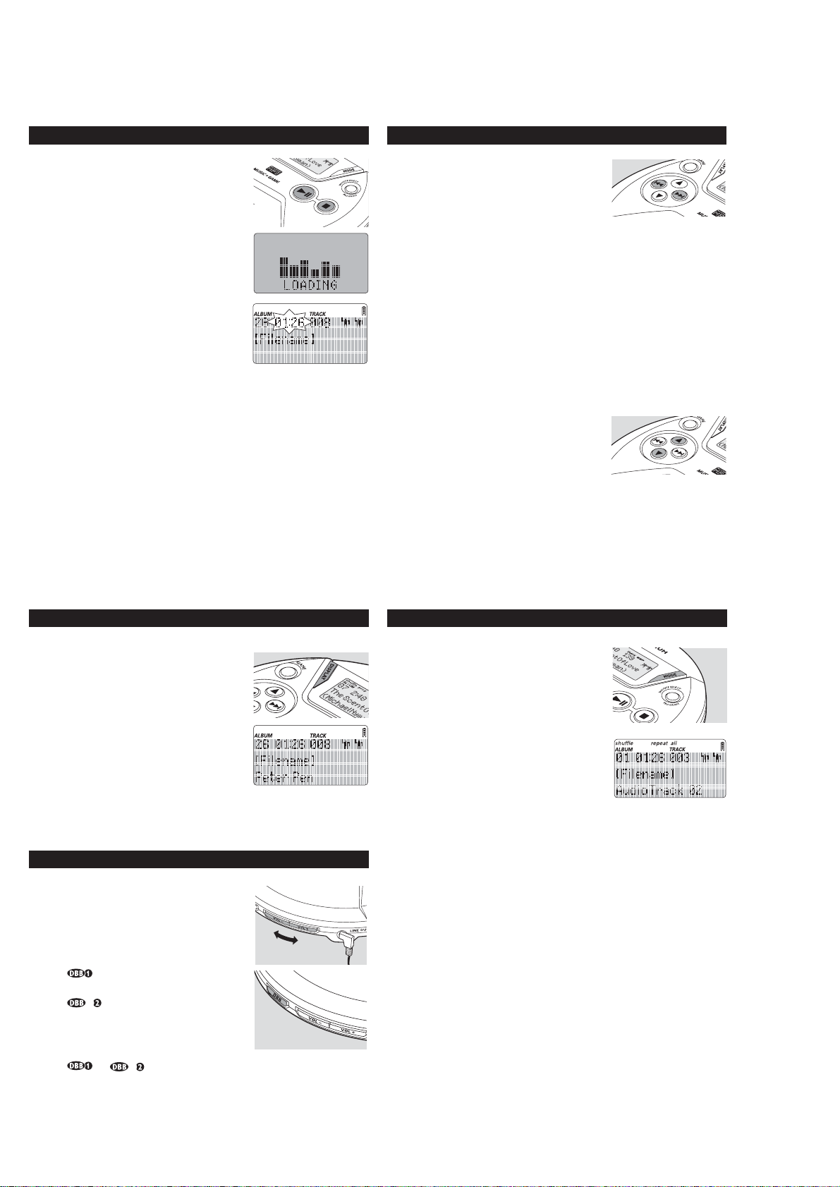
PLAYING A DISC
With this set you can play
–all pre-recorded audio CDs
–all finalized audio CDRs and CDRWs
–MP3-CDs (CD-ROMs with MP3 files)
1 Push the OPEN2 slider to open the CD
lid.
2 Insert a disc, printed side up, by pressing
gently on the disc´s center so that it fits
onto the hub. Close the lid by pressing it
down.
3 Press 2; to start playback.
eXpanium and LOADING are
displayed briefly. Playback starts.
The track type (CD or MP3), the
current track number and the elapsed
playing time are displayed. For an
MP3 track, the album number is also
displayed and the filename is scrolled
one time.
• Press 2; to interrupt playback.
Elapsed playback time flashes and the dancing animation
freezes.
•To resume playback press 2; again.
4 Press 9 to stop playback.
The total number of tracks, the track types (CD, MP3), the
number of albums on an MP3-CD and the total playing time (of
an audio disc only) are displayed.
5 To remove the disc, hold it by its edge and press the hub gently
while lifting the disc.
6 Press 9 again to switch off the played.
Notes:
– After pressing 2; it may take some time until the first MP3 track is played.
– The display clears automatically after 20 seconds if no controls are operated
in the stop mode.
SELECTING AND SEARCHING ON CDS
Selecting a track during playback
• Briefly press or § once or several
§
times to skip to the current, previous or
next track.
Playback continues with the selected
track, and the track’s number is displayed.
Searching for a passage during playback
1 Keep or § pressed to find a particular passage in a backward
§
or forward direction.
Searching starts while playback continues at low volume. After
2 seconds the search speeds up.
2 Release the button when you reach the desired passage.
Playback continues from this position.
Note:
–In shuffle, or repeat modes searching is only possible within the
particular track.
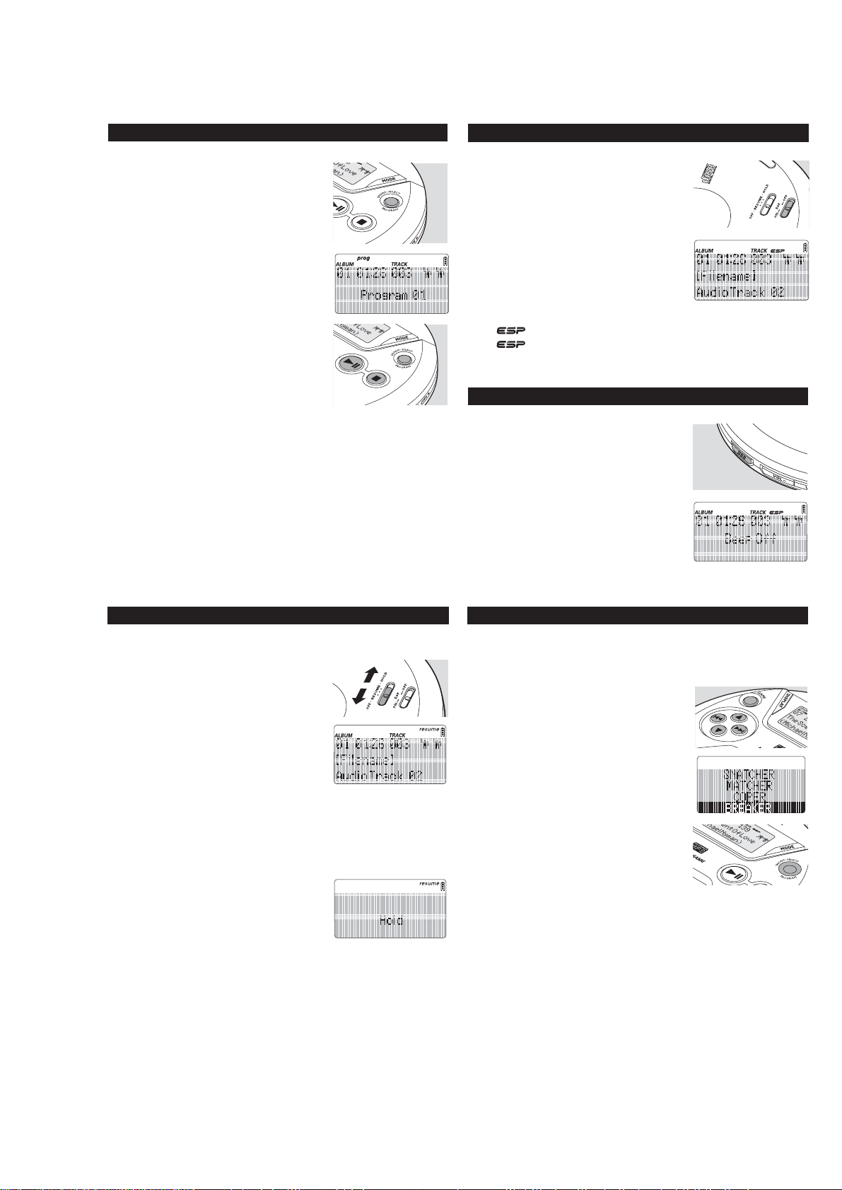
Selecting on MP3-CDs
Selecting an album during playback
• Briefly press 4 or 3 once or several
times to skip to the first track of the
current, previous or subsequent album.
The first track of the selected album
is played.
Selecting a track during playback
1 Keep 4 or 3 pressed to skip quickly to previous or subsequent
MP3 tracks.
Skipping starts and speeds up after 5 seconds.
2 Release the button at the desired track.
Playback continues with the selected track.
Note:
–To skip from track to track at low speed, use or §
§
.
DISPLAY INFORMATION
(for MP3 tracks only)
1 Press DISPLAY repeatedly during
playback to select the information to be
displayed:
– Filename: the track´s file name,
– Album: the album´s folder name,
– Artist: the artist´s name (if this ID3
tag information is available),
– Title: the track´s title (if this ID3
tag information is available),
– the track type.
2 The selected information is scrolled once.
The album number and track number are
displayed.
Note:
– The ID3 tag is part of an MP3 file and contains various track information such
as the track´s title or the artist´s name. Complete the ID3 tag information
with your MP3 encoder software before burning the MP3-CD.
VOLUME AND SOUND
Volume adjustment
• Adjust the volume by using VOL +/–.
DBB
Bass adjustment
1 Press DBB once or more to select the bass
enhancement options:
moderate bass enhancement is
activated.
strong bass enhancement
is activated.
2 Press DBB again to switch off the bass
enhancement options.
or disappears.
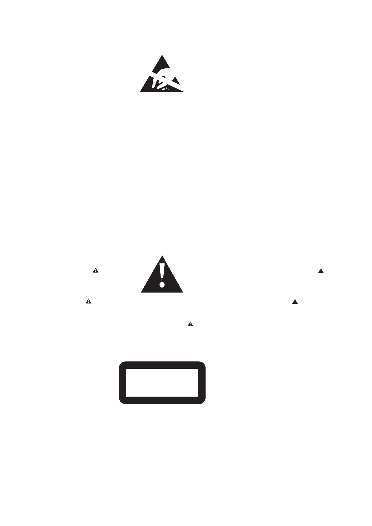
SELECTING DIFFERENT PLAYING POSSIBILITIES-MODE
1 Press MODE during playback as often as
required in order to activate one of the
following.
– shuffle all: All tracks of the disc are
played in random order once.
– shuffle repeat all: All tracks of the disc
are played repeatedly in random order.
– repeat: The current track is played
repeatedly.
– repeat all: The entire disc is played
repeatedly.
– shuffle album (with MP3-CDs only):
All tracks of the current album are played in random order once.
– shuffle repeat album (with MP3-CDs only):
All tracks of the current album are played repeatedly in random
order.
– repeat album (with MP3-CDs only):
All tracks of the current album are played repeatedly.
2 Playback starts in the chosen mode after 2 seconds.
•To return to normal playback, press MODE repeatedly until the
display shows no active modes.
Page 7
1-6
INSTRUTION FOR USE
PROGRAMMING TRACK NUMBERS
You can store up to 50 tracks to play in a
program. A single track may be stored more
than once in the program.
1 While playback is stopped, select a
track with or §§.
2 Press PROGRAM/SHOOT/SELECT to
store the track.
prog and the number of stored
tracks are displayed.
3 Select and store all desired tracks
in
this way.
4 Press 2; to start playback of your
selected tracks.
prog is shown and playback starts.
•You can review the program by pressing
PROGRAM/SHOOT/SELECT for more
than 3 seconds.
The display shows all the stored
tracks in sequence.
Note:
–If you try to store
more than 50 tracks,
FULL is displayed.
Clearing the program
•While playback is stopped, press 9 to clear program.
Program Clear is displayed once, prog goes off, and the
program is cleared.
Note:
– The program will also be cleared if the power supply is interrupted, or if the
CD-player lid is
opened, or if the set switches off automatically.
ESP/ POWER SAVE MODE
With a conventional portable CD-player you
might have experienced that the music
stopped e.g. when you were jogging. The
ELECTRONIC SKIP PROTECTION prevents loss
of sound caused by light vibrations and
shocks. Continuous playback is ensured.
However ESP does not prevent playback
interruptions during vigorous running. It
also does not protect the unit against
any damage caused by dropping!
• Adjust the ESP slider to ON/OFF
position to select the following:
– is shown and ESP is switched on.
– disappears. Powersaving are switched on for CD Audio
tracks to achieve the highest sound quality.
BEEP
A beep confirms that
you have pressed a
button or that the batteries are empty.
• During music mode only keep DBB
pressed for 2
seconds to switch beep
either on or off:
Beep On is displayed: Beep is
switched on.
Beep Off is displayed: Beep is
switched off.
RESUME AND HOLD
Storing the last position played – RESUME
You can store the last position played. When
restarting,
playback will continue from where
you have stopped.
1 Switch the slider to RESUME during
playback
to activate RESUME.
resume is shown.
2 Press 9 whenever you want to stop
playback.
3 Press 2; whenever you want to resume
playback.
resume shown
and playback continues from where you have
stopped.
•To deactivate RESUME, switch the slider to OFF.
resume goes
off.
HOLD – locking all buttons
You can lock all buttons of the set. When you
press any key, no action will be executed then.
1 Switch the slider to HOLD to activate
HOLD.
resume is shown and Hold is
displayed. All buttons are locked.
When pressing any key, Hold is displayed.
2 To deactivate HOLD, switch the slider to OFF.
resume resume disappears.
MUSIC AND GAMES
You can listen to music and play games at the same time. Select from 5
games: SNATCHER, MATCHER, COPTER, BREAKER and MUNCHER.
To start a game
1 If necessary, press 2; to switch on the
set.
2 Press GAME.
Display shows the games main
menu. The current game is
highlighted.
3 Press 3 or 4 to scroll through the list
of games.
4 To confirm your game selection, press
PROGRAM/ SHOOT/ SELECT.
5 Press 3 or 4 to scroll through the
game submenu.
Display shows Start, Level,
Speed, Top Score.
6 Press PROGRAM/ SHOOT/ SELECT to
confirm and start play.
How to control your game
Use the buttons on the set to navigate:
Up 3 Left Down 4 Right §
§
•Press PROGRAM/ SHOOT/ SELECT to SHOOT/ confirm an action.
End game
To quit the game function you can:
•Press GAME once or more until the display returns to the music
mode display.
•Press 9.
Note:
– This unit automatically switches off the beep signal when you select the
game mode during music playback. The beep signal automatically returns
when you quit GAME. For more details on the beep signal, please read the
BEEP chapter.
Page 8
1 - 7
SAFETY & WARNINGS
© WARNING
All ICs and many other semiconductors are susceptible to
electrostatic discharges (ESD). Careless handling during
repair can reduce life drastically.
When repairing, make sure that you are connected with the
same potential as the mass of the set via a wristband with
resistance. Keep components and tools at this potential.
ESD
ñ WAARSCHUWING
Alle IC´s en vele andere halfgeleiders zijn gevoelig voor
electrostatische ontladingen (ESD).
Onzorgvuldig behandelen tijdens reparatie kan de levensduur
drastisch doen vermindern. Zorg ervoor dat u tijdens reparatie
via een polsband met weerstand verbonden bent met hetzelfde
potentiaal als de massa van het apparaat.
Houd componenten en hulpmiddelen ook op ditzelfde potentiaal.
f ATTENTION
Tous les IC et beaucoup d´autres semi-conducteurs sont
sensibles aux décharges statiques (ESD). Leur longévite
pourrait être considérablement écourtée par le fait qu´aucune
précaution nést prise à leur manipulation.
Lors de réparations, s´assurer de bien être relié au même
potentiel que la masse de l´appareil et enfileer le bracelet
serti d´une résistance de sécurité.
Veiller à ce que les composants ainsi que les outils que l´on
utilise soient également à ce potentiel.
©
AVAILABLE ESD PROTECTION EQUIPMENT :
anti-static table mat large 1200x650x1.25mm 4822 466 10953
small 600x650x1.25mm 4822 466 10958
anti-static wristband 4822 395 10223
connection box (3 press stud connections, 1MΩ) 4822 320 11307
extendible cable (2m, 2MΩ, to connect wristband to connection box) 4822 320 11305
connecting cable (3m, 2MΩ, to connect table mat to connection box) 4822 320 11306
earth cable (1MΩ, to connect any product to mat or to connection box) 4822 320 11308
KIT ESD3 (combining all 6 prior products - small table mat) 4822 310 10671
wristband tester 4822 344 13999
d WARNUNG
Alle ICs und viele andere Halbleiter sind empfindlich
gegenüber elektrostatischen Entladungen (ESD).
Unsorgfältige Behandlung im Reparaturfall kann die
Lebensdauer drastisch reduzieren.
Sorgen Sie dafür, daß Sie im Reparaturfall über ein Pulsarmband mit Widerstand mit dem Massepotential des
Gerätes verbunden sind.
Halten Sie Bauteile und Hilfsmittel ebenfalls auf diesem
Potential.
©
Safety regulations require that the set be restored to its
original condition and that parts which are identical with
those specified be used.
Safety components are marked by the symbol
f
Les normes de sécurité exigent que l`appareil soit remis
à l`état d`origine et que soient utilisées les pièces de
rechange identiques à celles spécifiées.
Les composants de sécurité sont marqués
d
Bei jeder Reparatur sind die geltenden Sicherheitsvorschriften zu beachten. Der Originalzustand des Gerätes
darf nicht verändert werden. Für Reparaturen sind Originalersatzteile zu verwenden.
Sicherheitsbauteile sind durch das Symbol markiert.
SAFETY
i AVVERTIMENTO
Tutti IC e parecchi semi-conduttori sono sensibili alle scariche
statiche (ESD).
La loro longevità potrebbe essere fortemente ridatta in caso di
non osservazione della più grande cauzione alla loro
manipolazione. Durante le riparationi occorre quindi essere
collegato allo stesso potenziale che quello della massa
delápparecchio tramite un braccialetto a resistenza.
Assicurarsi che i componenti e anche gli utensili con quali si
lavora siano anche a questo potenziale.
ñ
Veiligheidsbepalingen vereisen, dat het apparaat in zijn
oorspronkeliijke toestand wordt teruggebracht en dat
onderdelen, identiek aan de gespecificeerde, worden toegepast.
De Veiligheidsonderdelen zijn aangeduid met het symbool
i
Le norme di sicurezza estigono che l´apparecchio venga
rimesso nelle condizioni originali e che siano utilizzati i
pezzi di ricambiago identici a quelli specificati.
Componenty di sicurezza sono marcati con
©
DANGER: Invisible laser radiation when open.
AVOID DIRECT EXPOSURE TO BEAM.
s Varning !
Osynlig laserstrålning när apparaten är öppnad och
spärren är urkopplad. Betrakta ej strålen.
©
After servicing and before returning the set to customer
perform a leakage current measurement test from all
exposed metal parts to earth ground, to assure no
shock hazard exists.
The leakage current must not exceed 0.5mA.
CLASS 1
LASER PRODUCT
∂ Advarsel !
Usynlig laserstråling ved åbning når sikkerhedsafbrydere
er ude af funktion. Undgå udsaettelse for stråling.
f
"Pour votre sécurite, ces documents doivent être utilisés par
des spécialistes agréés, seuls habilités à réparer votre
appareil en panne".
ß Varoitus !
Avatussa laitteessa ja suojalukituksen ohitettaessa olet alttiina
näkymättömälle laserisäteilylle. Älä katso säteeseen !
Page 9
2 -1
SERVICE HINTS
REPAIR POSITION COPPERSIDE
To get access to the copperside of the
printed board assembly proceed as follows:
1.Remove the bottom (3x) screws (2x of them under the
rubber-foot) and the up (2x) screws (in the CD-door)
2.Lift the bottom -cabinet
3.Supply the unit via external DC-socket
4.Take care that the door switch is closed during
measurements
REPAIR POSITION COMPONENTSIDE
To get access to the componentside of the
printed board assembly proceed as followed:
1.Remove the bottom (3x) screws (2x of them under the
rubber-foot) and the up (2x) screws (in the CD-door)
2.Open the CD-door
3.Lift the top-cabinet and put it backwards on the table
4.Supply the unit via the external DC-socket
5.Take care that the door switch is closed during
measurements
DISMANTLING THE CD-DOOR
To dismantle the CD-door proceed as follows:
1.Dismantle bottom and printed board/drive assembly
2.Disconnect the sticker
(flex-foil connector on the membrance keyboard)
3.Disconnect membrance keyboard
(flex-foil connector on copperside of printed board)
Remark:Do not use screwdrivers or tools .
Sharp edges could damage hinge or cabinet part.
4.Bend the cabinet rightwards downwards as indicated in
the picture above
Page 10

2 - 2
SERVICE TOOLS
Audio signal disc SBC429 4822 397 30184
Playability test disc SBC444 4822 397 30245
Test disc 5 (disc without errors ) + Test disc 5A(disc with dropout errors
black spots and fingerprints) SBC426/ SBC426A 4822 397 30096
ESD PROTECTION EQUIPMENT
Anti-static table mat large 1200x650x1.25mm 4822 466 10953
small 600x650x1.25mm 4822 466 10958
Anti-static wristband 4822 395 10223
Connection box (3press stud connections,1MΩ) 4822 320 11307
Extendible cable (2m,2MΩ ,to connect wristband to connection box) 4822 320 11305
Connecting cable (3m,2MΩ ,to connect table mat to connection box) 4822 320 11306
Earth cable (1MΩ , to connect any product to mat or to connection box) 4822 320 11308
KIT ESD3(combining all 6 prior products - small table mat) 4822 310 10671
Wristband tester 4822 344 13999
HANDLING CHIP COMPONENTS
Page 11

3 - 1
BLOCK DIAGRAM OF IC SAA7824HL
D2 D4 R1 R2
D1 D3
MONITOR
EXTFILTER
SENSE LPOWER
I
REF
V
REF_OUT
SCL
SDA
RAB
SILD
TEST1
TEST2
TEST3
TEST4
OSCIN
OSCOUT
CLK16
CLK4_12
CDT_RDY
CDT_DATA
CDT_CLK
SFSY
SUB
RCK
SBSY
STATUS
RESET
DC OFFSET COMPENSATION
VOLTAGE BUFFER
HF & LF CAPTURE
BIAS
GENERATOR
CONTROL
PART
MICRO
INTERFACE
TEST
TIMING
CD-TEXT
INTERFACE
INTERFACE
CONTROL
DECODER
MICRO-
CONTROLLER
INTERFACE
HFPASS FILTER
DATA SLICER &
THRESHOLD CON-
DEMODULATOR
ADDRESSER
SUBCODE
PROCESSOR
D1-D4
SUM
TROL
DIGITAL
PLL
EFM
SRAM
RAM
VERSATILE PINS
INTERFACE
MONITOR
ADC
ANTI ALIAS
DSIC ADC
CONTROL FUNCTION
PROCESSOR
PEAK
DETECT
LASER
POWER CON-
TROL LOGIC
AUDIO
KILL
LASER
OUTPUT
STAGES
MOTOR
CONTROL
ERROR
CORRECTOR
FLAGS
EBU
INTERFACE
SERIAL
DATA
INTERFACE
SERIAL
DATA
(LOOPBACK)
INTERFACE
DEM DAC
HEADPHONE
BUFFERS
LASER
RA
FO
SL
CSLICE
MOTO1
MOTO2
CFLG
DOBM
EF
SCLK
WCLK
DATA
SCLI
WCLI
SDI
DAC_VPO
DAC_RP
DAC_RN
DAC_LP
DAC_LN
DAC_VREF
DAC_GND
BUF_IN_R
BUF_IN_L
BUF_OUT_R
BUF_OUT_L
V1
V3 V5
V2
V4
LKILL
RKILL
BUF_VPOS
BUF_GND
Page 12

3 - 2
SYMBOL PIN DESCRIPTION
LPOWER 1 Laser power supply
EXTFILTER 2 10 nF capacitor for Laser start-up control
MONITOR 3 Laser monitor diode
SENSE 4 OPU ground reference point for MONITOR measurement
V
SSA1
5 Analogue ground 1
IREF 6 Reference current pin (24K
Ω resister to analogue ground)
V
DDA1
7 Analogue supply voltage 1
VREF_OUT 8 Servo reference voltage
D1 9 Diode v
oltage/current input (central diode signal input)
D2 10 Diode voltage/current input (central diode signal input)
D3 11 Diode voltage/current input (central diode signal input)
D4 12 Diode voltage/current input (central diode signal input)
R1 13 Diode voltage/current input (satellite diode signal input)
R2 14 Diode voltage/current input (satellite diode signal input)
CSLICE 15 10nF capacitor for adaptive HF dataslicer
V
DDA2
16 Analogue supply voltage 2
V
SSA2
17 Analogue ground 2
OSCOUT 18 Crystal/resonator output
OSCIN 19 Crystal/resonator input
V
SSA3
20 Analogue ground 3
DAC_GND 21 Audio DAC ground
DAC_RP 22 Audio DAC right channel differential output (positive)
DAC_RN 23 Audio DAC right channel differential output (negative)
DAC_VREF 24 Audio DAC decoupling point (10uF//100nF to ground)
DAC_LN 25 Audio DAC left channel differential output (negative)
DAC_LP 26 Audio DAC left channel differential output (positive)
DAC_VPOS 27 Audio DAC positive supply
BUF_VPOS 28 Audio buffer positive supply
BUF_IN_R 29 Audio buffer right input
BUF_OUT_R 30 Audio buffer right output
BUF_OUT_L 31 Audio buffer left output
BUF_IN_L 32 Audio buffer left input
BUF_GND 33 Audio buffer ground
LKILL 34 Kill output for left channel (configurable as open drain)
RKILL 35 Kill output for right channel (configurable as open drain)
CDT_RDY 36 CD-Text to micro ready flag
CDT_DATA 37 CD-Text data to micro
CDT_CLK 38 CD-Text micro clock
CFLAG 39 Correction flag output (open drain)
V
SSD1
40 Digital ground 1
V
DDD1
41 Digital supply voltage 1
SDI 42 Serial data input (loopback)
WCLI 43 Word clock input (loopback)
SCLI 44 Serial bit clock (loopback)
EF 45 C2 error flag
DATA 46 Serial data output
WCLK 47 Word clock output
SCLK 48 Serial clock output
CLK16 49 16MHz clock
CLK4_12 50 Configurable 4MHz or 12MHz clock
RESET 51 Power on reset (active low)
SDA 52 Micro interface data I/O line (open drain output)
SCL 53 Micro interface clock line
RAB 54 Micro interface R/W & load control line (4-wire)
SILD 55
Micro interface R/W & load control line (4-wire)
STATUS 56 Servo interrupt request line/decoder status register/DC offset value readback
RCK 57 Subcode clock
SUB 58 P to W subcode
SFSY 59 Subcode frame sync
SBSY 60 Subcode block sync
V
SSD2
61 Digital ground 2
DOBM 62 Bi-phase mark output (externally buffered)
V
DDD2
63 Digital supply voltage 2
RA 64 Radial actuator
FO 65 Focus actuator
SL 66 Sledge actuator
MOTO1 67 Motor output 1
MOTO2 68 Motor output 2
V
SSD3
69 Digital ground 3
V
DDD3
70 Digital supply voltage 3
V1 71 Versatile pin 1
V2 72 Versatile pin 2
V3 73 Versatile pin 3
V4 74 Versatile pin 4
V5 75 Versatile pin 5
TEST1 76 Test pin
TEST2 77 Test pin
TEST3 78 Test pin
TEST4 79 Test pin
LASER 80 Laser drive
SYMBOL PIN DESCRIPTION
PIN DESCRIPTIONS OF IC SAA7824HL
Page 13

3 - 3
SYMBOL
(1)
LFBGA
208
PIN
DIGITAL I/O LEVEL
APPL.
FUNC
PIN STATE
AFTER
RESET
DESCRIPTION
General Purpose Pins (fixed: 25 pins)
GPIO<24> A11 0- 3.3VDC tolerant I/O 0 General Purpose IO pin
GPIO<23> B11 0- 3.3VDC tolerant I/O 0 General Purpose IO pin
GPIO<22> A10 0- 3.3VDC tolerant I/O 0 General Purpose IO pin
GPIO<21> B10 0- 3.3VDC tolerant I/O 0 General Purpose IO pin
GPIO<20> A9 0- 3.3VDC tolerant I/O 0 General Purpose IO pin
GPIO<19> B9 0- 3.3VDC tolerant I/O 0 General Purpose IO pin
GPIO<18> A8 0- 3.3VDC tolerant I/O 0 General Purpose IO pin
GPIO<17> B8 0- 3.3VDC tolerant I/O 0 General Purpose IO pin
GPIO<16> A7 0- 3.3VDC tolerant I/O 0 General Purpose IO pin
GPIO<15>
F4 0- 3.3VDC tolerant I/O 0 General Purpose IO pin
GPIO<1 4>
G2 0- 3.3VDC tolerant I/O 0 General Purpose IO pin
GPIO<1 3>
F3 0- 3.3VDC tolerant I/O 0 General Purpose IO pin
GPIO<1 2>
G1 0- 3.3VDC tolerant I/O 0 General Purpose IO pin
GPIO<1 1>
F2 0- 3.3VDC tolerant I/O 0 General Purpose IO pin
GPIO<1 0>
F1 0- 3.3VDC tolerant I/O 0 General Purpose IO pin
GPIO< 9>
D3 0- 3.3VDC tolerant I/O 0 General Purpose IO pin
GPIO< 8>
E2 0- 3.3VDC tolerant I/O 0 General Purpose IO pin
GPIO< 7>
D4 0- 3.3VDC tolerant I/O 0 General Purpose IO pin
GPIO< 6>
E1 0- 3.3VDC tolerant I/O 0 General Purpose IO pin
GPIO< 5>
D2 0- 3.3VDC tolerant I/O 0 General Purpose IO pin
GPIO< 4>
D1 0- 3.3VDC tolerant I/O 0 General Purpose IO pin
GPIO< 3>
C2 0- 3.3VDC tolerant I/O 0 General Purpose IO pin
GPIO< 2>
C1 0- 3.3VDC tolerant I/O 0 General Purpose IO pin
GPIO<1 >
B1 0- 3.3VDC tolerant I/O 0 General Purpose IO pin
GPIO< 0>
A1 0- 3.3VDC tolerant I/O 0 General Purpose IO pin
8.4672 MHz o scillator (fixed: 5 pins)
XTAL 1I P4 A 6MHz clock input
XTAL 1O R3 A 6MHz clock output
CD_CLOCK K1 0- 3.3VDC tolerant O CD clock output (gated)
VDDA1 R2 Analog supply Oscillator 1
VSSA1 R1 Analog ground Oscillator 1
Voltage Supply PLL s (fixed: 2 pins )
VDDA3 N2 Analog supply PLLs
VSS A3 N1 Analog ground PLLs
PLL (fixed 1pin)
CLKO1 F 15 0- 3.3VDC tolerant O 256fs audio output clock
LCD Interface (fixed: 13 pins)
LCD_WE K3 O Write Enable
LCD_RW_WR A16 O 6800 read/write select
8080 active ‘high’ write enable
PIN DESCRIPTIONS OF IC SAA7752
EBI
LCD
ADC
IIS
Input
SDAC
TIC
SMC
AHB
Arbiter
SDRAM
Controller
ETU
bridge
AHB to APB
IIS
bus
Output
CTU
Watchdog
Timers
10-bits
Interface
Clock
Shop
PMU
SAA7752
AHB
wrapper
ROM
JTAG/TCB
AHB
SRAM
Decoder
AHB
wrapper
ARM720T
Interrupt
Controller
CD-Block
Master
Decoder
Slave
IIC Interface
IIC Interface
General
Purpose I/O
UART
IrDA
OSCs PLLs
Page 14

3 - 4
CDB_NCRST_NHRD
Y
D5 O CD engine reset line/Host is ready to receive the next frame
CDB_C LA B C9 0- 3.3VDC tolerant I IIS/EIAJ input bit clock
CDB_D AAB C7 0- 3.3VDC tolerant I IIS/EIAJ serial data
CDB_WSAB
C8 0- 3.3VDC tolerant I IIS/EIAJ word clock
CDB_E FA B D9 0- 3.3VDC tolerant I IIS/EIAJ error flags
CDB_V 4_SUB D8 0- 3.3VDC tolerant I Versatile pin 4:single wire subcode/EIAJ subcode data bits
CDB_C FLAG_SBSY D6 0- 3.3VDC tolerant I Absolute time sync/EIAJ subcode block sync
CDB_S FSY D7 0- 3.3VDC tolerant I EIAJ subcode frame sync
CDB_RCK C6 O EIAJ subcode clock output
Audio DAC (SDAC, fixed 5 pins)
DAC_VREFP R17 analog positive reference for SDAC
DAC_REFN P16 analog negative reference for SDAC
VOUTL P15 A Analog left LINE output
VOUTR R16 A Analog right LINE output
DAC_VDD N14 I Supply digital part of the SDAC
EBI (fixed: 49 pins)
EBI_NCS<2> G16 O Chip Selected 2
EBI_NCS<1> T10 O Chip Selected 1
EBI_NCS<0> U10 O Chip Selected 0
EBI_SDNCS<0> H3 O External SDRAM selection1 and SDRAM selection0
EBI_WEN J2 O Write enable not (for SDRAM only)
EBI_A<20> J1 6 I/O EBI address
EBI_A<19> H 16
I/O
EBI address
EBI_A< 18> F14 O EBI address
EBI_A<17> G14 O EBI address
EBI_A<16> H14 O EBI address
EBI_A<15> J1 4 O EBI address
EBI_A<14> R9 O EBI address
EBI_A<13> T9 O EBI address
EBI_A<12> U9 O EBI address
EBI_A<11> R8 O EBI address
EBI_A<10> T8 O EBI address
EBI_A< 9> U8 O EBI address
EBI_A< 8> P11 O EBI address
EBI_A< 7> R7 O EBI address
EBI_A< 6> P10 O EBI address
EBI_A< 5> U7 O EBI address
EBI_A< 4> P9 O EBI address
EBI_A< 3> T7 O EBI address
EBI_A< 2> P8 O EBI address
EBI_A<1> R6 O EBI address
EBI_A< 0> U6 O EBI address
EBI_D<15> T6 0- 3.3VDC tolerant I/O EBI data
EBI_D<14> U5 0- 3.3VDC tolerant I/O EBI data
EBI_D<13> T5 0- 3.3VDC tolerant I/O EBI data
EBI_D<12> U4 0- 3.3VDC tolerant I/O EBI data
SYMBOL
(1)
LFBGA
208
PIN
DIGITAL I/O LEVEL
APPL.
FUNC
PIN STATE
AFTER
RESET
DESCRIPTION
LCD_E_RD B15 O 6800 active ‘low’ enable
8080 active ‘high’ write enable
LCD_DB<0> D14 0- 3.3VDC tolerant I/O Data input 0/Data output 0
LCD_DB<1> B17 0- 3.3VDC tolerant I/O Data input 1/Data output 1
LCD_DB<2> C14 0- 3.3VDC tolerant I/O Data input 2/Data output 2
LCD_DB<3> C16 0- 3.3VDC tolerant I/O Data input 3/Data output 3
LCD_DB<4> D13 0- 3.3VDC tolerant I/O Data input 4/Data output 4
LCD_DB<5> A17 0- 3.3VDC tolerant I/O Data input 5/Data output 5/serial clock
LCD_DB<6> C13 0- 3.3VDC tolerant I/O Data input 6/Data output 6/Serial data input
LCD_DB<7> B16 0- 3.3VDC tolerant I/O Data input 7/Data output 7/Serial data output
LCD_CSB C1 2 O Chip Select (active low)
LCD_RS D1 2 O ‘high’ Data register select
‘low’ Instruction register select
10-bit ADC (fixed: 9 pins)
GPA<4> A5 A Analog General Purpose pin 4
GPA<3> B5 A Analog General Purpose pin 3
GPA<2> J3 A Analog General Purpose pin 2
GPA <1>M4A Analog General Purpose pin 1
GPA <0> N3 AAnalog General Purpose pin 0
VREFP <1 > M3 A 10-bit ADC Reference voltage 1
VREFP <0 > L 2 A 10-bit ADC Reference voltage 0
VDDA4 M 2 A nalog supply 10-bit ADC
VSS A4 M1 Analog ground 10-bit ADC
IIS input (fixed: 3 pins)
BCKI 1 J 15 0- 3.3VDC tolerant I Bitclock input (external)
WSI1 H15 0- 3.3VDC tolerant I Wordselect input (external)
DATAI 1 G1 5 0- 3.3VDC tolerant I Serial data input (external)
IIS output (fixed: 3 pins)
BCKO 1 M14 I/O Tri-state Bitclock output (external)
WSO1 F16 O Tri-state Wordselect output (external)
DATAO 1 E16 O Output/Low Serial data output (external)
JTAG (fixed: 5 pins)
JTAG_NTRST K15 0- 3.3VDC tolerant I JTAG Reset Input
JTAG_TCK
U12 0- 3.3VDC tolerant I JTAG Clock Input
JTAG_TMS K16 0- 3.3VDC tolerant I JTAG Mode Select Input
JTAG_TDI T13 0- 3.3VDC tolerant I JTAG Data Input
JTAG_TDO U 13 O JTAG Data Output
IIC slave Interface (fixed: 3 pins)
SCL_SLAVE P12 0- 3.3VDC tolerant I/O Serial clock IIC Slave
SDA_SLAVE R12 0- 3.3VDC tolerant I/O Serial data IIC Slave
A0_SLAVE T12 0- 3.3VDC tolerant I Address selection Slave
IIC master interface (fixed: 2 pins)
SDA_MASTER R13 0- 3.3VDC tolerant I/O IIC data I/O line (open drain output)/
UART Serial Data Input
SCL_MASTER P13 0- 3.3VDC tolerant I/O IIC clock line output/
UART Serial Data Output
CD Block Decoder (fixed: 10 pins)
CDB_CRQ_NERDY C5 0- 3.3VDC tolerant I Communication request line/CD engine is ready to receive the next
frame
SYMBOL
(1)
LFBGA
208
PIN
DIGITAL I/O LEVEL
APPL.
FUNC
PIN STATE
AFTER
RESET
DESCRIPTION
PIN DESCRIPTIONS OF IC SAA7752
Page 15

3 - 5
VSSE_EBI F17 Peripheral (I/O) ground SAA7752 for EBI pads
VSSE_EBI L14 Peripheral (I/O) ground SAA7752 for EBI pads
Not connected pins (fixed: 2 pins)
NC D15 Not connected
NC A4 Not connected
NC B2 Not connected
NC A2 Not connected
NC D17 Not connected
NC D16 Not connected
NC C15 Not connected
NC C17 Not connected
NC N4 Not connected
NC P3 Not connected
NC P2 Not connected
NC P1 Not connected
NC A6 Not connected
NC B6 Not connected
NC K2 Not connected
NC E15 Not connected
NC B3 Not connected
NC A3 Not connected
NC B4 Not connected
NC B14 Not connected
NC A15 Not connected
NC B13 Not connected
NC A14 Not connected
NC E14 Not connected
NC T17 Not connected
NC U17 Not connected
NC T16 Not connected
NC R15 Not connected
NC U16 Not connected
NC M17 Not connected
NC K17 Not connected
NC H17 Not connected
NC G17 Not connected
NC J17 Not connected
NC L17 Not connected
NC N17 Not connected
NC P14 Not connected
NC R14 Not connected
NC U15 Not connected
NC T15 Not connected
NC T14 Not connected
NC N15 Not connected
NC U14 Not connected
NC C4 Not connected
SYMBOL
(1)
LFBGA
208
PIN
DIGITAL I/O LEVEL
APPL.
FUNC
PIN STATE
AFTER
RESET
DESCRIPTION
EBI_D<11> T4 0- 3.3VDC tolerant I/O EBI data
EBI_D<10> U3 0- 3.3VDC tolerant I/O EBI data
EBI_D<9> T3 0- 3.3VDC tolerant I/O EBI data
EBI_D<8> P7 0- 3.3VDC tolerant I/O EBI data
EBI_D<7> U2 0- 3.3VDC tolerant I/O EBI data
EBI_D<6> P6 0- 3.3VDC tolerant I/O EBI data
EBI_D<5> U1 0- 3.3VDC tolerant I/O EBI data
EBI_D<4> R5 0- 3.3VDC tolerant I/O EBI data
EBI_D<3> T2 0- 3.3VDC tolerant I/O EBI data
EBI_D<2> P5 0- 3.3VDC tolerant I/O EBI data
EBI_D<1> T 1 0- 3.3VDC tolerant I/O EBI data
EBI_D<0> R4 0- 3.3VDC tolerant I/O EBI data
EBI_S DCLKOUT J1 O SDRAM clock
EBI_CKE<0> H4 O SDRAM clock enable
EBI_DQM<1> T11 O SDRAM data mask 1
EBI_DQM<0> U 11 O SDRAM data mask 0
EBI_NRAS R10 O SDRAM: row address strobe
SMC: byteWr0 (byte write enable for byte 0... active LOW)
EBI_NCAS R11 O SDRAM column address strobe
SMC: byteWr1 (byte write enable for byte 1... active LOW)
EBI_N OE H2 O EBI output enable
UART (fixed: 3pins)
UART_DIR_TX D10 O
UART_REQ_RX C10 0- 3.3VDC tolerant I
UART_CLK D11 0- 3.3VDC tolerant I/O
Mode Selection pins SAA7752 (fixed: 3 pins)
MODE<2> L16 0- 3.3VDC tolerant I
MODE<1> M15 0- 3.3VDC tolerant I
MODE<0> M16 0- 3.3VDC tolerant I
Wake-up input pin SAA7752 (fixed: 1 pin)
WAKE_UP L 1 0- 3.3VDC tolerant I Wake up input pin
Reset input pin SAA7752 (fixed: 1 pin)
NRESET_IN L15 0- 3.3VDC tolerant I System Reset Input
Reset output pin SAA7752 (fixed: 1 p in)
RESET_OUT N1 6 O Reset output
Digital supplies SAA7752 (fixed: 6 pins)
VDDI1 L4 Core supply SAA7752
VSSIS1 L 3 Core ground and substrate SAA7752
VDDI2 G 4 Core supply SAA7752
VSSI2 G3 Core ground SAA7752
VDDI3 E4 Core supply SAA7752
VSSI3 E3 Core ground SAA7752
Peripheral supplies SAA7752 (fixed: 4 pins)
VDDE3V3 J4 Peripheral (I/O) supply SAA7752 (3.3V)
VSSE3V3 K4 Peripheral (I/O) ground SAA7752
VDDE_EBI E17 Peripheral (I/O) supply SAA7752 for EBI pads
VDDE_EBI K14 Peripheral (I/O) supply SAA7752 for EBI pads
SYMBOL
(1)
LFBGA
208
PIN
DIGITAL I/O LEVEL
APPL.
FUNC
PIN STATE
AFTER
RESET
DESCRIPTION
PIN DESCRIPTIONS OF IC SAA7752
Page 16

3 - 6
PIN DESCRIPTIONS OF IC SAA7752
BLOCK DIAGRAM OF IC SC111259A
SYMBOL
NC C3 Not connected
NC H1 Not connected
NC A13 Not connected
NC A12 Not connected
NC B12 Not connected
208
PIN
DIGITAL I/O LEVEL
LFBGA
(1)
APPL.
FUNC
VC VG VIN12
CF1
ERR1
CF2
ERR2
VR
CF3
ERR3
CF1
ERR1
VR
OE
CF2
ERR2
VR
OE
CF3
ERR3
VR
OE
Motor Driver
SAWTOOTH RSTB
VC VG VIN12
Motor Driver
SAWTOOTH RSTB
VC VG VIN34
Motor Driver
SAWTOOTH RSTB
CH1
CH2
CH3
PIN STATE
AFTER
RESET
DESCRIPTION
VIN12
OUT1A
OUT1B
PGND1
OUT2A
OUT2B
PGND2
VIN34
OUT3A
OUT3B
PGND3
CF4
ERR4
CGND
VG
C2H
C1H
C1L
C2L
WAKE
CHGON
CLK
SLEEP
OE
VC
VREF
RSTB
VG V C VIN
CHARGE
PUMP
VIN
CONTROL
VC
BANDGAP
REFERENCE
VC VC VIN
VC VG VIN34
CF4
ERR4
VR
OE
Motor Driver
SAWTOOTH RSTB
DCIN
CH4
SAW
GEN
VIN
DCIN
DCIN VC
DCIN
DETECT
OSC1
SAW
GEN2
VIN
ST
ARTUP
VIN
VC
OUT4A
OUT4B
PGND4
DCIN
INM2
RF2
VIN
CHGSW
RS
RF1
INM1
VC
VREF
DTC
VOUT
VDET
Page 17

3 - 7
PIN DESCRIPTIONS OF IC SC111259A
Pin# Symbol Pin Description
1SLEEP Sleep input
2WAKE Wake input
3VRReference Voltage Input(Motor driver)
4ERR4 Control signal input(CH4)
5CF4 Phase correction capacitor connect (CH4)
6CF3 Phase correction capacitor connect (CH3)
7ERR3 Control signal input(CH3)
8ERR2 Control signal input(CH2)
9CF2 Phase correction capacitor connect (CH2)
10 CF1 Phase correction capacitor connect (CH1)
11 ERR1 Control signal input(CH1)
12 OUT1A Positive drive output(CH1)
13 GND H-bridge driver ground
14 OUT1B Negative drive output(CH2)
15 VIN12 H-bridge driver voltage supply(CH1,CH2)
16 OUT2B Negative drive output(CH2)
17 GND H-bridge driver ground
18 OUT2A Positive drive output(CH2)
19 OUT3A Positive drive output(CH3)
20 GND H-bridge driver ground
21 OUT3B Negative drive output(CH3)
22 VIN34 H-bridge driver voltage supply(CH3,CH4)
23 OUT4B Negative drive output(CH4)
24 GND H-bridge driver ground
25 OUT4A Positive drive output(CH4)
26 VG
27
28 C1H Charge pump capactitor connect
29 C1L Charge pump capactitor connect
30 C2L Charge pump capactitor connect
31 VIN Battery voltage supply
32 RSTB Reset block output
33 CHGSW Transistor drive output for battery charger
34 RS OP-Amp non-inverting input for battery charger
35 INM2 Error amplifier inverting input for battery charger
36 RF2 Error amplifier output for battery charger
37 DCIN DC power supply from AC adaptor
38
39 VREF Voltage reference circuit output
40 DTC Max duty control voltage input for power management
41 VOUT PWM output for power managenent
42 VC Power management power supply
43 CGND Internal ground
44 RF1 OP-Amp output for power management
45 INM1 OP-Amp inverting input for power management
46 CLK Clock input
47
48 CHGON Charge enable for battery charger
C2H Charge pump capactitor connect
VDET DCIN over voltage and VIN low voltage detect putput
OE Output enable for motor driver
Charge pump output
Page 18

3 - 8
3 - 8
t
C
patible
t
t
SERVICE TEST PROGRAM - FLOW CHART
STOP button pressed not in any step returns
*
to begin of Service Testprogram.
To leave Service Testprogram press STOP to
*
switch off.
Door switch is ignored → CD door can be opened.
*
Volume up/down buttons function independentely
*
of the service testprogram.
DISPLAY TEST
COMPACT DISC TEST
To enter Service
Testprogramm hold
PLAY & PREV buttons
depressed while pressing
power on and door must be open.
Display shows:
Service Mode
KEY CODE TEST
SERVICE PLAY MODE
key
"NEXT"
triggered ?
y
display
"
DisplayPattern1
key
"NEXT"
triggered?
y
display
"
DisplayPattern2
key
"NEXT"
red?
trigge
y
display
"
DisplayPattern3
key
"
"
STOP
triggered?
y
key
"
y
key
n
y
display "--"
Key test table
"
"
Display button
pressed?
The set puts out error
messages if any problem is
detected in the difference
play states.
see table2.
N
7
MODE 9rc
y
y
y
n
x = door switch
y = inner switch
"0" = closed
"1" = open
n
key "NEXT"
pressed ?
Slide moves
outside
x = focus status
" " = focus ok
"-" = focus error
n
key "DBB"
pressed ?
toggle play mode
between "normal" and
"
D-RW com
n
key "PREV"
pressed ?
y
Slide moves inside
until inner switch is
activated
ESA-Flag = play mode
Flag lite = CD-RW compatible
Flag off = normal
n
key "NEXT"
pressed ?
y
Slide moves
"
outside
Mode
"
triggered?
n
"Stop"
triggered?
n
key "MODE"
pressed ?
y
Disc motor turns
clockwise
(accelerate)
n
key "PREV"
pressed ?
y
Slide moves inside
until inner switch is
activated
n
key "PROG"
pressed ?
y
Disc motor turns
counter-clockwise
(brake)
n
key "MODE"
pressed ?
y
Disc motor turns
clockwise
(accelerate)
n
y
n
key "PROG"
pressed ?
y
y
Disc motor turns
counter-clockwise
(brake)
key "STOP"
pressed ?
n
key "STOP"
pressed ?
n
y
n
Set key Code Set key Code Set key Code
STOP Exit PLAY 4 DISPLAY 8
any key
pressed?
display the
corresponding Code from
the Key Table
for RC: show "RC"
ALBUM - 1 PREV 5 MODE 9
y
ALBUM + 2 NEXT 6
GAME 3 PROGRAM
RC key Code RC key Code RC key Code
STOP Exit ALBUM - 1rc ALBUM + 2rc
PREV 5rc PLAY 4rc
table1
n
y
see table1
n
key "PLAY"
pressed ?
Servo Tes
"
n
"
n
display "S xy"
key "PLAY"
pressed ?
Focus Test
display "xF"
and "ESA-Flag"
"
key "PLAY"
pressed and
n
focus ok ?
Disc Motor Tes
Pattern1
Pattern2
Pattern3
Radial Tes
display "xF"
and "yd"
and "ESA-Flag"
key
"PLAY" pressed and
focus ok and
speed ok ?
y
display "xF"
and "yd"
and "zr"
and "ESA-Flag"
key "NEXT"
pressed ?
y
CUE-MODE
track servo jumps
16 tracks forward
x = focus status
" " = focus ok
"-" = focus error
n
x = focus status
" " = focus ok
"-" = focus error
n
16 tracks backward
y =disc speed
" " = speed ok
"-" = speed error
y = disc speed
" " = speed ok
"-" = speed error
key "PREV"
pressed ?
y
REVIEW-MODE
track servo jumps
ESA-Flag = play mode
Flag lite = CD-RW compatible
Flag off = normal
z = on track status
" " = on track
"-" = not on track
n
ESA-Flag = play mode
Flag lite = CD-RW compatible
Flag off = normal
key "STOP"
pressed ?
y
key "STOP"
pressed ?
y
F .... Fatal error W .... Warning
Error
Type Description
number
1000
W focus error
Triggered when the focus is lost during playing the CD.
1001
n
W radial error
1002
W sledge in error
Triggered when the radial servo is off-track for a certain time during playing the CD.
The sledge did not reach its inner position (innerswitch is closed) before
1003
W sledge out error
approximately. 6 seconds have passed by - innerswitch or sledgemotor problem.
The sledge did not come out of its inner position (innerswitch is open) before
1004
approximately 250ms have passed by - innerswitch or sledgemotor problem.
W DRAM filling error
The DRAM controller was not able to connect two consecutive audio frames.
1005
Therefore, the µP had to issue a direct audio connection that produces audible clicks.
W jump error
1006
W subcode error
n
1008
No valid subcode for a certain time during play.
W turntable motor error
Generated when the CD could not reach 75 % of speed during start
Triggered when the jump destination could not be found within
a certain time.
-up within a certain
time. Discmotor problem
1020
F focus search error
The focus point has not been found within a certain time.
table 2
Page 19

3 - 9
3 - 9
BLOCKDIAGRAM
DC JACK
Headphone
Page 20

4 -1
4 -1
COMBI BOARD - CIRCUIT DIAGRAM
CONTROL/ESP PART
1
A
B
C
D
E
F
G
H
I
GPIO_14
NRESET_IN
EBI_NRAS
EBI_NOE
EBI_NCS_0
J
K
L
1234
23
+3V2
5400
10K
3472
25
A(1)
24
A(2)
23
A(3)
22
A(4)
21
A(5)
20
A(6)
19
A(7)
18
A(8)
8
A(9)
7
A(10)
6
A(11)
5
A(12)
4
A(13)
3
A(14)
2
A(15)
1
A(16)
48
A(17)
15
12
11
28
26
47
37
EPROM
256Kx8/128Kx16
0
1
2
3
4
5
6
7
0
8
A
2M-1
9
10
11
12
13
14
15
16
RB
RP
W
G
E
BYTE
27
0
1
2
3
4
5
6
7
D
8
9
10
11
12
13
14
15
A-1
M29W200BT-70N6
NC
46
EBI_DQM_0
EBI_DQM_1
2459
29
DQ(0)
31
DQ(1)
33
DQ(2)
35
DQ(3)
38
DQ(4)
40
DQ(5)
42
DQ(6)
44
DQ(7)
30
DQ(8)
32
DQ(9)
34
DQ(10)
36
DQ(11)
39
DQ(12)
41
DQ(13)
43
DQ(14)
45
DQ(15)
9
10
13
14
16
17
100n
7445
45 8
+3V2_SDRAM
100n
2451
2450
100n
100n
2449
7404
MT48LC4M16A2TG-7E
VDDQ
DQML15
DQMH39
DQ0
2
DQ(0)
DQ(1)
DQ(2)
DQ(3)
DQ(4)
DQ(5)
DQ(6)
DQ(7)
DQ(8)
DQ(9)
DQ(10)
DQ(11)
DQ(12)
DQ(13)
DQ(14)
DQ(15)
GPIO_20
GPIO_21
GPIO_22
DQ1
4
DQ2
5
DQ3
7
DQ4
8
DQ5
10
DQ6
11
DQ7
13
DQ8
42
DQ9
44
DQ10
45
DQ11
47
DQ12
48
DQ13
50
DQ14
51
DQ15
53
+3V2_DSP
100K
SSSS8
1407
7
5
BANK0
MEMORY
ARRAY
(4,096x256x16)
SENSE AMPLIFIERS
DQMH
DQML
I/O GATING
DQM DATA LOGIC
READ DATA LATCH
WRITE DRIVERS
DATA INPUT REGISTER DATA OUTPUT REGISTER
NC
36
40
54
SCL_MASTER
SDA_MASTER
A(0:17)
GPIO_10
GPIO_11
GPIO_12
GPIO_13
GPIO_14
GPIO_15
GPIO_16
3461
3462
3463
100K
100K
GPIO_17
GPIO_18
GPIO_19
GPIO_23
7405
BC847BW
+3V2_DSP
100K
F462
6
1
F463
2
F464
3
4
GPIO_0
GPIO_2
GPIO_3
GPIO_4
GPIO_5
GPIO_7
GPIO_8
GPIO_9
3453
56
67
2408
100n
2407
100n
CKE
37
CLK
38
CS_
19
WE_
16
CAS_
17
DECODE
COMMAND
RAS_
18
20BA0
21BA1
A0 23
24A1
A2 25
26A3
29A4
30A5
31
A6
32A7
ADDRESS REGISTER
33A8
34A9
A10 22
35A11
6
10n2426
10n2428
2427 10n
+3V2_DSP_1
3455
3456
100K
F468
3
4
100n
2429 10n
1408
ESE11MV
SSSS8
1409
2841
8
6
1427394349
VDD
BANK0
ROW-
ADDR
LATCH &
DECODER
ROW
ADDR
MUX
BANK
CTRL
LOGIC
COLUMN
ADDR
COUNTER/
LATCH
COLUMN
DEDCODER
7
4
3
2
1
5
1
REFRESH
COUNTER
VSSQVSS
100K
F465
F425
F426
F427
124652
3454
F466
F467
CTRL
LOGIC
2425 10n
100K
2406
MODEREG
F405
2409
47u 16V
EBI_CKE_0
EBI_SDCLKOUT
EBI_SDNCS_0
EBI_SDWEN
EBI_NCAS
EBI_NRAS
A(12)
A(13)
A(0)
A(1)
A(2)
A(3)
A(4)
A(5)
A(6)
A(7)
A(8)
A(9)
A(10)
A(11)
3422 470R
3424
3425 4K7
3427 4K7
3428 4K7
3431 4K7
3433
3435 4K7
3439 4K7
3441
3447
3448
3449
10n2431
2432 10n
2430 10n
2434 10n
F470
F469
1
2
2K7
1404
SKQT
34
12
3457
3458
100K
F471
34
F472
1405
SKQT
12
78
2452
4K73426
4K73429
4K73432
4K7
4K73434
4K73437
4K7
4K73443
39K3444
4K73446
4K73450
10K3464
2438 10n
F474
F473
2464
9
100n
2411
100n
2410
NRESET_IN
10n
10n2441
10n2440
2439
3459
100K
1406
SKQT
34
12
2465
390p
390p
100n
2412
100n
F442
1n0
2463
EBI_NCS_0
EBI_NOE
EBI_NCAS
EBI_NRAS
EBI_DQM_0
EBI_DQM_1
EBI_CKE_0
EBI_SDCLKOUT
EBI_SDWEN
EBI_SDNCS_0
10n2443
2442 10n
2444 10n
F475
GPIO_4
GPIO_5
GPA_0
GPIO_11
GPIO_12
GPIO_10
GPIO_13
VOUTL
VOUTR
2413
MODE_0
MODE_1
MODE_2
100n
A(0:17)
DQ(0:15)
10n2445
VOUTR
GPIO_21
GPIO_22
GPIO_20
2414
2446 10n
VOUTL
2454
10
+2V7
100n
100n
2415
N15
N16
L15
L1
M16
M15
L16
U10
T10
G16
H2
R11
R10
U11
T11
H4
J1
U6
A(0)
R6
A(1)
P8
A(2)
T7
A(3)
P9
A(4)
U7
A(5)
P10
A(6)
R7
A(7)
P11
A(8)
U8
A(9)
T8
A(10)
R8
A(11)
U9
A(12)
T9
A(13)
R9
A(14)
J14
A(15)
H14
A(16)
G14
A(17)
F14
H16
J16
R4
DQ(0)
T1
DQ(1)
P5
DQ(2)
T2
DQ(3)
R5
DQ(4)
U1
DQ(5)
P6
DQ(6)
U2
DQ(7)
P7
DQ(8)
T3
DQ(9)
U3
DQ(10)
T4
DQ(11)
U4
DQ(12)
T5
DQ(13)
U5
DQ(14)
T6
DQ(15)
J2
H3
F417
A1
F418
B1
F419
C1
C2
F421
D1
F422
D2
E1
F424
D4
E2
D3
F1
F428
F2
F429
G1
F430
F3
F432
G2
F434
F4
F408
A7
F407
B8
F460
A8
F412
B9
A9
F444
F411
B10
A10
F413
F406
B11
A11
B12
A12
A13
H17
K17
M17
U17
T17
R16
P15
U15
R14
P14
T15
T14
P17
T16
100n
2456
10u 10V
910
+3V2_DSP
F400
+1V8_DSP
K14
J4
PERIP
RESET
RESET_OUT
NRESET_IN
WAKE_UP
MODE_0
MODE_1
MODE_2
EBI_NCS_0
EBI_NCS_1
EBI_NCS_2
EBI_NOE
EBI_NCAS
EBI_NRAS
EBI_DQM_0
EBI_DQM_1
EBI_CKE_0
EBI_SDCLKOUT
0
1
2
3
4
5
6
7
8
9
10
EBI ADDR
11
12
13
14
15
16
17
18
19
20
0
1
2
3
4
5
6
7
EBI DATA
8
9
10
11
12
13
14
15
EBI_WEN
EBI_SDNCS_0
GPIO_0
GPIO_1
GPIO_2
GPIO_3
GPIO_4
GPIO_5
GPIO_6
GPIO_7
GPIO_8
GPIO_9
GPIO_10
GPIO_11
GPIO_12
GPIO_13
GPIO_14
GPIO_15
GPIO_16
GPIO_17
GPIO_18
GPIO_19
GPIO_20
GPIO_21
GPIO_22
GPIO_23
GPIO_24
GPIO_25
GPIO_26
GPIO_27
VINM
VINR
VINL
VOUTR_HP
VOUTL_HP
VOUTR
VOUTL
L3MODE_A0
L3DATA_SDA
L3CLOCK_SCL
SELECT_L3_IIC
TEST1
VREF
VREF_HP
PERIP
K4
H1
3481 G15
11
+3V2_DSP
F401
2400
L4G4E4
C4
VDDI
VDDD_CODEC
SYSTEM
AUDIO PLAYER
7402
SAA7750
EBI
MEMORY CARD INTERFACE
SSA
VSSI
1
VSSD_CODEC
L3
E3
C3
G3
L14
11
12 13 14 15 16
+2V7
+2V6_DSP
4401
4402
F402
100n
R17
N14
E17
VDDA_DA
VDDD_FLASH
Φ
CD BLOCK DECODER
REMOTE CONTROL
OSCILLATORS
LCD INTERFACE
VSSA_DA
VSSD_FLASH
F17
P16
U14
F403
VDDA_AD
10 BIT ADC
TEST PINS
VSSA_AD
L17
N17
3400
VADCP
VADCN
JTAG
J17 G17
10R
USB
PLL
R15
VDDA_HP
IIC
IIS
UART
VSSA_HP
U16
+3V2_DSP_1
VDDA
CDB_CRQ_NERDY
CDB_NCRST_NHRDY
CDB_DAAB
CDB_WSAB
CDB_V4_SUB
CDB_CFLAG_SBSY
SLAVE
MASTER
MCI_DAT_0
TEST_DAT_1
TEST_DAT_2
TEST_DAT_3
USB_CONNECT_N
LCD_RW_WR
LCD DB
UART_NDTR
UART_NDSR
UART_NDCD
UART_NCTS
UART_RST_NRTS
UART_REQ_RX
UART_DIR_TX
UART_IO_NRI
VSSA
M1
VREFP_1
VREFP_0
CDB_CLAB
CDB_EFAB
CDB_SFSY
CDB_RCK
A0_SLAVE
MCI_CLK
MCI_CMD
USB_DP
USB_DM
USB_VUSB
XTAL1O
XTAL2O
LCD_WE
LCD_E_RD
LCD_CSB
LCD_RS
DATAO1
DATAO2
SPDIFO
UART_CLK
P2N2M2
NTRST
GPA_0
GPA_1
GPA_2
GPA_3
GPA_4
GPA_5
GPA_6
GPA_7
DO_0
XTAL1I
XTAL2I
CLKO1
BCKI1
WSI1
DATAI1
BCKO1
WSO1
F404
TCK
TMS
TDO
SCL
SDA
SCL
SDA
DI_0
+1V8_DSP
3401
10R
10K
100n
2448
2405
100n
2455
100n
R2
2401
100n
100n
2402
K15
U12
K16
T13
TDI
U13
N3
M4
J3
B5
A5
B6
A6
B7
M3
L2
2416
10u 10V
C5
D5
C9
C7
C8
D9
D8
D6
D7
C6
T12
P12
R12
P13
R13
A4
A2
B2
B4
A3
B3
K1
K2
C17
D17
D16
C15
F416
P4
R3
N4
P3
K3
A16
B15
D14
0
B17
1
C14
2
C16
3
D13
4
A17
5
C13
6
B16
7
C12
D12
F15
J15
H15
G15
M14
F16
E16
E15
3469
+3V2_DSP
A14
B13
A15
B14
D11
C11
C10
D10
E14
D15
NC
R1P1N1
2403
+3V2_DSP_1
3411
100R
2417
100n
2418
10n
6M
GPA_1
GPA_0
3470
10K
SCL_MASTER
SDA_MASTER
CX-5F
10K
100n
2453
100n
2404
100n
GPIO_3
MODE_2
MODE_1
MODE_0
NRESET_IN
F414
F410
F409
NKEY2
NKEY1
3412
3413
3452
100K
100K
100K
3414
3468
100K
8M_CLK
2457
56p
1411
2458
56p
NRESET_IN
5401
5402
100p
2461
2462
10K
3471
2419
100p
1
2447
100n
2
3
F461
6
7
10K
3408
10K
3415
3416
100K
3436 1K
3438
3442
3445
PLAY
100p
E0
E1
E2
SCL
WC_
3402
3409
100K
3417
10K
+3V2_DSP
VCC
1K0
1K03440
1K0
1K0
100R
100K
3460
+3V2_DSP
100K
3418
0
2420
8
SDA
VSS
3403
100K
3451
4
3404
3473
3419
100K
3481
2422
100p
5
100K
100K
100K
3420
10K
4K7
100p
7403
M24C02
3405
3474
2460
100p
2421
F423
100K
100K
BC857BW
7401
3477
15R
3478
15R
100K
3406
3475
100K
CDB_CLAB
CDB_DAAB
CDB_WSAB
CDB_EFAB
CDB_V4_SUB
CDB_CFLAG_SBSY
CDB_SFSY
CDB_RCK
SCL_MASTER
SDA_MASTER
+3V2_DSP
1K5
10R
3423
6.3V22u
6401
2423
100p
12 13 14 15 16 17
+3V2
100K
3407
3476
100K
3421
6402
BZX384-C3V9
F449
F450
F451
F452
F453
F454
F455
F456
F457
F458
F459
GPA_0
GPA_1
GPA_2
GPA_3
GPA_4
F445
F446
F447
F448
+3V2_DSP_1
3430
100n
BZX384-C3V9
2424
17
1400
FMN
1
2
3
4
5
6
7
8
9
10
11
12
13
9
8
5
4
3
1401
2
TCX0101-11
1
7
MT MT
6
11FMN-SMT
12 13
11
F431
10
F433
9
F435
8
F436
7
F437
6
F438
5
F439
4
F440
3
F441
2
1
1403
ESD
1400 A17
4401 A11
1401 G17
1403 I17
4402 A11
1404 J7
5400 G3
1405 J8
5401 H14
1406 J9
5402 H14
6401 I16
1407 J4
1408 J7
6402 I16
1409 J5
7401 F15
1411 G14
2400 A11
2401 B13
2402 B13
2403 B14
2404 B14
2405 B14
2406 B6
2407 B6
2408 B7
2409 B7
2410 B9
2411 B9
2412 B9
2413 B9
2414 B10
2415 B10
2416 D13
2417 D13
2418 F14
2419 I15
2420 I15
2421 I15
2422 I15
2423 I16
2424 I16
2425 I6
2426 I6
2427 I6
2428 I6
2429 I7
2430 I7
2431 I7
2432 I7
2434 I7
2438 I8
2439 I9
2440 I9
2441 I9
2442 I9
2443 I9
2444 I9
2445 I9
2446 I10
2447 J14
2448 B15
2449 B4
2450 B5
2451 B5
2452 B9
2453 B14
2454 K10
2455 B14
2456 K10
2457 G14
2458 G14
2459 G3
2460 G15
2461 I14
2462 I14
2463 C9
3400 A12
3401 A13
3402 B15
3403 B15
3404 B15
3405 B15
3406 B16
3407 B16
3408 C15
3409 C15
3411 D14
3412 D14
3413 D14
3414 D14
3415 D15
3416 D15
3417 D15
3418 D15
3419 D15
3420 F15
3421 F16
3422 G8
3423 G16
3424 G8
3425 G8
3426 G8
3427 G8
3428 G8
3429 G8
3430 G16
3431 G8
3432 H8
3433 H8
3434 H8
3435 H8
3436 H15
3437 H8
3438 H15
3439 H8
3440 H15
3441 H8
3442 H15
3443 H8
3444 H8
3445 H15
3446 H8
3447 H8
3448 H8
3449 H8
3450 H8
3451 I15
3452 D14
3453 J5
3454 J6
3455 J6
3456 J6
3457 J7
3458 J8
3459 J9
3460 C15
3461 H5
3462 H5
3463 H5
3464 I8
3468 D14
3469 I13
3470 I13
3471 I14
3472 G2
3473 C15
3474 C15
3475 C16
3476 C16
3477 F16
3478 G16
7402 C11
7403 J1
7404 B4
7405 I5
7445 I4
F400 A10
F401 A11
F402 A12
F403 A1
F404 A13
F405 A7
F406 H10
F407 H10
F408 H10
F409 C14
F410 C14
F411 H10
F412 H10
F413 H10
F414 C14
F416 G13
F417 G10
F418 G10
F419 G10
F421 G10
F422 G10
F423 J16
F424 G10
F425 G6
F426 G6
F427 H6
F428 H1
F429 H10
F430 H10
F431 H1
F432 H10
F433 H17
F434 H1
F435 H1
F436 H1
F437 H17
F438 H17
F439 H17
F440 H17
F441 H17
F442 B9
F444 H10
F445 F16
F446 F16
F447 G16
F448 G16
F449 B16
F450 B16
F451 B16
F452 B16
F453 B16
F454 B1
F455 B16
F456 B16
F457 C16
F458 C16
F459 C16
F460 H10
F461 J14
F462 J5
F463 J5
F464 J5
F465 J6
F466 J6
F467 J6
F468 J6
F469 J7
F470 J7
F471 J8
F472 J8
F473 J9
F474 J9
F475 J9
5
2
0
7
0
7
7
6
A
B
C
D
E
F
G
H
I
J
K
L
Page 21

4 - 2
4 - 2
COMBI BOARD - CIRCUIT DIAGRAM
AUDIO PART
A
B
C
D
E
1300 B10
2300 B5
2301 C4
2304 A6
2305 A7
2306 A1
VOUTR
V_HP
2310
GPIO_15
VOUTL
100n
3337
470K
470K
2307 A5
2308 B3
2309 B6
2310 B1
2311 B3
2312 C9
1
F301
3324
F307
BC857BW
7308
100K
3350
2306
3344
10K
2321
2313 C9
2314 C6
2315 C2
2316 C10
2317 C3
2318 C3
22u6.3V
2315
22u6.3V
3368
2K2
3330
16V10u
3369
2K2
100K
3351
100K
F305
2319 D6
2320 D7
2321 D1
2322 D5
2323 E6
2324 E6
2
6K8
3313
BC817-40W
7311
6K8
3363
2329
2328
390p
2325 E8
2326 E9
2327 C6
2328 B2
2329 D2
2330 A7
3309
12K
390p
22R
3317
7305
BC817-40W
22R
3353
3359
12K
4K7
100n
2317
3357
2331 D7
3300 B5
3301 B4
3302 B5
3303 C4
3304 C4
3316
100n
2308
2311
BC817-40W
100n
100n
2318
4K7
7300
GPIO_17
3306 C4
3307 A6
3308 D8
3309 A2
3310 A5
3312 A7
7302
BC817-40W
100K
3306
3355
47K
3301
F303
100K
3335
3313 B2
3315 B6
3316 B3
3317 B3
3318 B8
3324 B1
4
2301
18K
4u7
V_HP
100K
BC857BW
7301
3303
10K
3336
3330 B2
3335 E4
3336 E4
3337 B1
3341 B7
3344 C1
3304
2307
2u2
100K
2322
2u2
7306
BC807-25
7309
BC847BW
6K8
3300
3352
53
470K
3302
470K
3360
56K
3345 C6
3349 C8
3350 C1
3351 C2
3352 E5
3353 C3
3310
56K
V_HP
2300
F308
100n
GPIO_16
3354 C8
3355 E4
3356 C6
3357 C3
3358 A8
3359 D2
VREF
4K7
100p
7307
BC847BW
VREF
4K7
100p
3365
100K
3345
100K
3307
5
2304
6
3356
2319
3
2
3360 D5
3361 D7
3362 D6
3363 D2
3364 E8
3365 E6
V_HP
8
4
3315
180K
2309
33p
V_HP
3362
180K
2323
33p
7303-B
TDA1308T
2314
1u
2327
8
7303-A
4
TDA1308T
2324
1u
7
100n
1
7313
BC847BW
3366 E8
3367 E8
3368 A2
3369 D2
3370 A8
3371 D8
220u4V
2305
1K0
3341
4V
2320
220u
76
330R
BAV70
330R
2330
3312
6300
6301
BAS316
1K0
3361
5301 B9
5302 B9
5303 B10
5304 C10
5305 D8
6300 B7
100p
3354
2331
100p
F309
V_HP
6301 C7
6302 C10
7300 C3
7301 B4
7302 B4
7303-A D6
8
3370
10R
3358
15R
3318
3349
3308
15R
3371
10R
+3V2
5305
2325
3364
10R
330R
330R
4V100u
7303-B A6
7304 B8
7305 B2
7306 D5
7307 B6
7308 B1
BC817-40
7304
3366
100K
7310
BC817-40
VREF
3367
2326
100K
7309 E5
7310 C8
7311 C2
7313 E7
F300 D9
F301 A1
F302 A10
F303 C4
F304 C10
F305 C2
F306 A9
F307 D1
F308 D5
F309 E8
F310 E9
F311 B10
F312 C10
F313 B10
910
F306
100p
F310
47u 6.3V
2313
100p
2312
F300
5302
5301
F302
F311
5303
F312
6302
BZX384-C10
ESD
F314
5304
F313
F304
4
2
1
3
RC
5
TC38
220p
2316
F314 B10
A
1300
B
C
ESD
D
E
1
23
4
5
67
8910
Page 22

4 - 3
4 - 3
COMBI BOARD - CIRCUIT DIAGRAM
CD DRIVE PART
A
B
C
D
1800 B1
1801 D5
2804 A9
1
2
3
4
5
6
7
8
9
10
11
12
13
14
15
16
17
18
1800
20
SFV
2805 A9
2806 A9
2807 B6
2808 B8
2809 D9
2810 D3
2811 D3
2812 D3
2813 D3
2814 D4
2815 D4
2816 D4
2817 D5
2818 D5
2819 E8
2820 E6
2821 E7
2822 E7
2823 A8
2824 A8
2825 A8
2826 A8
3800 A8
3801 A8
3802 A9
3803 A8
3804 A9
3805 A8
3806 A9
3807 A4
3808 A5
3809 A5
3810 A6
3812 B3
3813 B8
3815 B4
3818 E9
3819 C10
3820 A7
3823 D1
3824 D4
3827 B3
3890 C3
4801 E6
6800 D10
7802 C4
7803 C7
F800 A7
1 234567
75
10K
3820
27
F800
28
INNERSWITCH
70
69
V171V272V373V474V5
VSSD3
VDDD3
7803
SAA7824HL
BUF_VPOS
BUF_IN_L
BUF_IN_R29BUF_OUT_L
30
32
31
67
68
66
MOTO1
MOTO2
LKILL
BUF_GND
34
35
33
65
SL
FO
RKILL
CDT_RDY36CFLAG
+3V2_CD18
F802
F803
F804
F805
F806
F807
F808
F809
F810
F812
F813
F814
F815
Focus+
TrackTrack+
Focus-
3827
4R7
GPIO_2
4K7
3890
0R
3812
3815
1M0
7802
BC807-25
0R
3807
F801
F816
F817
19
F818
16V
3823
1R0
2810
100n
2811
100n
2812
100u
2813
47n
3824
24K
2814
4u7
2815
F819
F822
100n
2816
+3V2_CD18
0R
22n
2817
3808
4u7
2818
100n
+3V2_CD18
0R
F811
1801
CSTCC
8M467
3809
1
2
3
4
5
6
7
8
9
10
11
12
13
14
15
16
17
18
19
20
F820
LPOWER
EXTFILTER
MONITOR
SENSE
VSSA1
IREF
VDDA1
VREF_OUT
D1
D2
D3
D4
R1
R2
CSLICE
VDDA2
VSSA2
OSCOUT
OSCIN
VSSA3
+3V2_CD18
10R
3810
100n
2807
76
77
78
80
79
TEST1
TEST2
TEST3
TEST4
LASER
DAC_RN
DAC_RP22DAC_VPOS
DAC_VREF
DAC_GND21DAC_LN25DAC_LP26BUF_OUT_R
23
24
3800
3801
3803
3805
63
64
62
RA
VDDD2
CDT_CLK
CDT_DATA
38
37
39
F801 B4
F802 B1
F803 B1
0R
0R
0R
61
DOBM
VSSD2
STATUS
RESET_
CLK4_12
CLK16
WCLK
VDDD1
VSSD1
40
F804 B1
F805 B1
F806 B1
F807 B1
F808 B1
F809 B1
F810 C1
F811 C6
F812 C1
F813 C1
F814 C1
F815 C1
F816 C1
F817 C1
F818 C1
F819 E4
F820 E6
F821 D8
8910
MOTO1
2808
SBSY
SFSY
SUB
RCK
SILD
RAB
SCL
SDA
SCLK
DATA
SCLI
WCLI
SDI
2823
X
EF
3n3
2824
XX
3813
100n
60
59
58
57
56
55
54
53
52
51
50
49
48
47
46
45
44
43
42
41
3n3
0R
1n5
2825
F823
F821
2819
X
2826
1n5
+1V8_CD18
CDB_SFSY
CDB_V4_SUB
CDB_RCK
CDB_CLAB
CDB_WSAB
CDB_DAAB
CDB_EFAB
+3V2_CD18
100n
10K
3802
4K7
3804
4K7
3806
4K7
3818
2806
3n3
33n
2804
1n5
2809
1n5
2805
+3V2_CD18
10K
F824
Sledge
Focus
Radial
3819
6800
BAT54A
SCL_MASTER
SDA_MASTER
NRESET_IN
GPIO_0
F822 B4
F823 C8
F824 D10
A
B
C
D
E
X = OPEN
1 234
8M_CLK
+3V2_CD18
4801
0R
2820
100u 16V
2821
100n
2822
100n
CDB_CFLAG_SBSY
E
5678910
Page 23

4 - 4
4 - 4
COMBI BOARD - CIRCUIT DIAGRAM
POWER SUPPLY PART
123
6200
LD1117
4
2
IN
O1
3
O2
5
6
O3
7
8
16V47u
2210
A
SL03
6207
GND
O4
1
7236
BC817-25
3218
3294
4u7
220R
12K
2200
3295
2248
F252
1u
3K3
1200
0.7A
ICP-S0.7
2203
1u
2202
B
F251
4.5V
S93
C
2216
100n
6204
BZX384-C10
F250
D
E
F
6203
3215
BAT54 COL
DC JACK
1201
10K
3219
150K
7214-B
LM358D
5
F261
ESD
6205
SL03
F278
3233
82K
3221
6
3224
150K
S40
C
4M7
3227
100K
+3V2
F253
7213
BC868
3245
C
100R
7214-A
C
100n
LM358D
1
2221
C
8
4
C
3251 470K
C
2228
C
3257
3254
100p
C
8K2
F254
0V
C
1R0
1R0
3256
G
CHARGING CIRCUIT
C....only for charging version
%....tolerance 1%
+3V2
+A
4.1V
C
3273
BC857BW
7224
C
3275
C
3283
470K
470K
0.1V
7227
BC847BW
ACCU_IN DETECTION
470K
3274
+A
C
2M2
3272
C
H
+3V2
X
C
TEMP.
I
10K
3279
3278
150K
C
t
3285
NTH5G
456789
VCC
F265
4u7
REF
SLEEP 1
CHGON 48
CONTROL
SI2305DS
RSTB 32
VREF 39
WAKE 2
CGND
ERR4 4
ERR3 7
ERR2 8
ERR1 11
7238
+1V8
3202
+3V2
10K
F262
1.2V
0V
OE 47
0V
CLK 46
0V
3.2V
1.3V
C2L 30
1.4V
C1L 29
5.2V
C1H 28
7.2V
C2H 27
9.5V
CHARGE PUMP
VG 26
43
1.3V
1.3V
CF4 5
1.3V
1.3V
CF3 6
1.3V
3VR
1.3V
2233
1.3V
CF2 9
220p
1.3V
1.3V
10CF1
5205
+1V8_CD18
+1V8_DSP
+2V6_DSP
6212
8K2
8K2
BC847BW
3209
2223
100n
2224
100n
2217
2230
220p
2231
220p
+1.3V
2237
+3V2
BZX384-C3V9
3203
7205
3222
2227
4201
4203
F269
100n
2234
220p
6211
2K7
10n
BZX384-C3V9
7200
BC807-25
BC847BW
1K0
3210
VCC
+3V2
10K
3262
3228
3248
470K
+3V2
%
10K
3259
%
1u
10K
3267
Focus
Radial
to CD-PART
5202
+3V2_SDRAM
5204
+3V2_DSP
+3V2_CD18
7204
SI2305DS
BAT54C
3214
100K
3825
100K
7206
+2V6_EN
4206
VCC
3299
100K
2222
Sledge
5203
6216
15K
10K
3298
100K
F275
3205
3211
+3V2
10K
1u
BC847BW
4211
+2V6_EN
GPIO_9
100K
8
4
100u 16V
+3V2
C
S00
C
2201
3225
82K
+3V2
BC857BW
7209
110K
3
2
GPIO_23
4205
7
C
3238
2239
16V
100u
F273
C
5201
10u
100n
3280
68K
8K2
220K
+3V2
C
C
10K
10K
3239
3247
/ACCU
GPA_3
S20
4
5
3220
3223
3260
6201
SL03
3200
68K
7
FB
LX I|O
SYNC
CTRL
OFF
GND
6
8
+DC
SHUTDOWN
2220
100p
3235
220K
Track-
Track+
3K3
11
SL+
SL-
1202
4209
TO CD-PART
Focus-
Focus+
4210
F257
12345
GPA_3
GPIO_19
GPA_2
+A
12K
3293
+A
F258
DSP PART
7203
TEA1208T
ILIM
2
3234
0R
9
0R
F260
100K VR
3201
47K
U_|D
100K
3286
3
1
3207
3297
47K
470R
2247
2211
VCC
F264
6.3
2212
100n
100u
68n
DC/DC CONVERTER - S30
7217
3226
1M0
2232
22K
12
6
2219
F272
10
100u
78
1u
0.3V
0.2V
2.8V
0.6V
1.5V
0V
0.4V
4.1V
0.7V
0.4V
4.3V
4.1V
4.1V
2238
F259
INNERSWITCH
ZH
3206
330R
38 VDET
45 INM1
25 OUT4A
4V100u
7237
BC847BW
SC111259AFTA
VOUT41
DTC40
VC42
RF144
RS34
CHGSW33
VIN31
STARTUP
GEN2
OSC
SAW
DET
DCIN
RF236
INM235
DCIN37
PGND424
OUT4B23
PGND320
OUT3B21
OUT3A19
VIN3422
PGND217
OUT2B16
OUT2A18
PGND113
OUT1B14
RSTB
OUT1A12
VIN1215
SERVO DRIVER - C40
+3V2
+2V6
3208
100K
GPIO_7
VCC
4204
D60
++
+
SAWTH.RSTB
CH4
DRIVER
MOTOR
SAWTH.RSTB
CH3
DRIVER
MOTOR
SAWTH.RSTB
CH2
DRIVER
MOTOR
SAWTH.
CH1
DRIVER
MOTOR
6213
7208
SI2305DS
2209
BANDGAP
+
GEN
SAW
OE
VR
ERR1
CF1
VCVGVIN
OE
VR
ERR1
CF1
VCVGVIN
OE
VR
ERR1
CF1
VCVGVIN
OE
VR
ERR1
CF1
VCVGVIN
+1V8
6214
BZX384-C3V9
BZX384-C3V9
5206
5207
1u0
2251
2218
3212
220K
from DSP-PART
VCC
47K
3230
3229
F276
7216
VCC
3276
GPIO_19
1M0
3826
6218
BAT54 COL
3829
330K
+2V7
16V100u
3288
F256
3290
100K
POWER_OFF
CHARGE_ON
VCC
X
10K
3281
100K
1n0
2235
+A
3264
3266
1011 12 13
7207
BC807-25
22K
4K7
+2V6
6215
2241
3241
2225
1M0
X = OPEN
3501
3828
680K
6217
7235
BC847BW
330K
7232
BAT54 COL
BC847BW
1u0
GPIO_2
GPIO_19
+DC
X
1M0
10n
3250
10K
3502
4M7
BAT54 COL
+2V6
F277
+3V2
22u
2252
+2V6 +2V6
3830
100K
WAKE
+A
BC857BW
7215
1M0
3249
3263
8K2
X
100K
VCC
3204
100K
GPIO_8
+2V6_EN
4207
2245
7229
BC847BW
100K
3287
2205
100n
BAT54 COL
6206
GPIO_18
MOTO1
WAKE
6210
BAT54C
3217
3831
WAKE
120K
3
1
10K
+A
3242
3284
3258
47K
4u7
TEA1208T
U_|D
2M2
2M2
2250
7230
CTRL
ILIM
2
3216
NRESET_IN
4K7
3231
3236
4K7
3246
2M2
+3V2
74LV132D
7202-2
74LV132D
4
5
100n
1K2
7202-1
1
2
7
FB
OFF
8
3252
2M2
3253
10M
VCC
714
+2V6
3261
7234
BC847BW
SYNC
GND
6
+AVCC
2226
100n
VCC
714
10R
3213
68K
4
LXI|O
5
10K
3232
BC857BW
7210
+A +3V2
10M
3
3277
6
150K
3243
2206
10u
5200
SL03
6202
3237
4K7
3244
330K
BC847BW
7218
2M2
3255
3291
120K
2244
7202-3
74LV132D
9
10
2240
100n
220n
3292
100K
100n
3240
VCC
714
4100u
2207
47K
2229
+A
6208
BAT54 COL
2246
2249
10n
7202-4
74LV132D
12
13
100n
SHUTDOWN
8
+3V2
F255
4208
100u 4
7211
BC847BW
3289
330K
VCC
14
7
F266
11
5208
3V3
+A
+1V8
PLAY
GPA_0
RC
GPA_4
+2V6_EN
+3V2_DSP_1
1200 A3
1201 C2
1202 I5
2200 A2
2201 B4
2202 A3
2203 A3
2205 B11
2206 A12
2207 A13
2209 B7
2210 A1
A
2211 B6
2212 B6
2216 C1
2217 F8
2218 A9
2219 D6
2220 D5
2221 E3
2222 E9
2223 E8
2224 E8
2225 E10
2226 E12
B
2227 D8
2228 F3
2229 F13
2230 F8
2231 G8
2232 G5
2233 G8
2234 G8
2235 G9
2237 H8
2238 H6
2239 I4
C
2240 H12
2241 D10
2244 G12
2245 B10
2246 G13
2247 C6
2248 A2
2249 A13
2250 H11
2251 A9
2252 B10
3200 A5
D
3201 A5
3202 A8
3203 A8
3204 H10
3205 A9
3206 I6
3207 B6
3208 I6
3209 B8
3210 B8
3211 B9
E
3212 B9
3213 A12
3214 I9
3215 B2
3216 C11
3217 A11
3218 A1
3219 C3
3220 C4
3221 C3
3222 C8
3223 C4
F
3224 D3
3225 D4
3226 D5
3227 D4
3228 D8
3229 D9
3230 D9
3231 D11
3232 D12
3233 D3
3234 E5
3235 E5
G
3236 E11
3237 E12
3238 E4
3239 E4
3240 E12
3241 E10
3242 E11
3243 E12
3244 E12
3245 E3
3246 E11
H
3247 F4
3248 F8
3249 F10
3250 F10
3251 F3
3252 F11
3253 F11
3254 F3
3255 F12
3256 F3
3257 F3
3258 I11
3259 G8
3260 G5
I
3261 I11
3262 D8
3263 G10
3264 H9
3266 I9
3267 G8
3272 H3
3273 H3
3274 H2
3275 I3
3276 G9
3277 H12
3278 I1
3279 I1
3280 I4
3281 G9
3283 I3
3284 H11
3285 I1
3286 A6
3287 A10
3288 A10
3289 F13
3290 B10
3291 G12
3292 H12
3293 G5
3294 B1
3295 B2
3297 B6
3298 C9
3299 D9
3501 G10
3502 G10
3825 I9
3826 H9
3828 H10
3829 I9
3830 C10
3831 C11
4201 D8
4203 E8
4204 A7
4205 A4
4206 C9
4207 B10
4208 A13
4209 G5
4210 H5
4211 G9
5200 A12
5201 A4
5202 H8
5203 I9
5204 I8
5205 H7
5206 I7
5207 I7
5208 I13
6200 A1
6201 A5
6202 B12
6203 B1
6204 C1
6205 C2
6206 E11
6207 B1
6208 G13
6210 H11
6211 I8
6212 I8
6213 I7
6214 I7
6215 C10
6216 I9
6217 H10
6218 I9
7200 A8
7202-1 G11
7202-2 H11
7202-3 H12
7202-4 G13
7203 A5
7204 I9
7205 A8
7206 A9
7207 A10
7208 A7
7209 D4
7210 E12
7211 E13
7213 E2
7214-A E3
7214-B C3
7215 F10
7216 F9
7217 D7
7218 F12
7224 H3
7227 I3
7229 C10
7230 B11
7232 C10
7234 I11
7235 I10
7236 A1
7237 I6
7238 I7
F250 D1
F251 B1
F252 A2
F253 E2
F254 F3
F255 A13
F256 A9
F257 H5
F258 H5
F259 H6
F260 H5
F261 C2
F262 C8
F264 A7
F265 A7
F266 A13
F269 E8
F272 F6
F273 E4
F275 D9
F276 E9
F277 A10
F278 C2
12
3
456789
1011 12 13
Page 24

4 - 5
4 - 5
COMBI BOARD - LAYOUT DIAGRAM
COMPONENT SIDE VIEW
Page 25

4 - 6
4 - 6
COMBI BOARD - LAYOUT DIAGRAM
COPPER SIDE VIEW
Page 26

5 - 1
5 - 1
MECHANICAL PARTSLIST
EXPLODED VIEW DIAGRAM
401
406
407
408
screw 1.7x6 CR
plastite (2x)
409
411
401 3140 117 66021 CD-DOOR-ASSY-EXP521
402 3140 117 67451 KEY-GAMES-ASSY-EXP521
403 3140 117 67461 KEY-SHOOT-ASSY-EXP521
404 3140 110 51821 LCD MODULE - EXP521
406 3140 117 66991 SLIDER-DOOR-OPEN-AX5215
402
404
403
413
417
418
419
414
416
412
407 3140 111 22611 SPRING-SLIDER-OPEN-AX5203
408 3140 117 66941 CABINET-AX5215-ASSY-1
409 3140 117 67001 KNOB-VOLUME-AX5215
411 3140 117 67011 KNOB-DBB-AX5215
412 3140 111 01501 SPRING-CD DOOR EXP521
413 3140 111 22621 SPRING-BATTERY-SET, +/- AX5203
414 2422 549 45374 CD DRIVE DA50
416 3140 114 47581 DAMPER-AX5203
417 3140 111 22571 SPRING BATTERY, +VE AX5203
418 3140 111 22581 SPRING BATTERY, -VE AX5203
419 3140 111 22601 SPRING BATTERY CHARGE-AX5203
421 3140 117 67351 BOTTOM-AX5202-ASSY-1
422 3140 117 67161 SLIDER-HOLD-AX5203
423 3140 117 66471 DOOR-BATTERY-2A-AX5203
424 3140 111 22631 SPRING BATTERY-DOOR +/- AX5203
426 3140 117 67031 DOOR-BATTERY-3A-AX5215-ASSY
427 3140 114 49361 RUBBER-FOOT
Note: Only these parts mentioned in the list are
normal service parts.
screw 1.4x2.5
plastite (12x)
423
424
426
screw 1.7x9 CR
plastite (3x)
422
427
421
Page 27

6 - 1
6 - 1
ELECTRICAL PARTSLIST - COMBI BOARD
- MISCELLANEOUS - - CAPACITORS -
1200 2422 086 11012 FUSE 0,7A 50V 2241 4822 126 14043 1µF +80-20% Y5V 16V
1201 2422 026 05086 CONNECTOR SUPP H 1P 2244 4822 126 13879 220nF +80-20% 16V
1202 2422 025 12918 CONNECTOR H 6P 2245 2238 586 59812 100nF +80-20% Y5V 50V
1300 2422 026 05317 SOCKET PHONE H 1P 2246 2238 586 59812
1403 2422 025 17034 SOCKET FFC H 11P 2247 3198 017 36830 68nF X7 16V
1404 2422 128 02863 SWITCH-TACT 2248 4822 126 14472 1µF 10% X7 10V
1405 2422 128 02863 SWITCH-TACT 2249 3198 032 15190 100µF 20% 4V
1406 2422 128 02863 SWITCH-TACT 2250 2238 586 59812 100nF +80-20% Y5V 50V
1407 2422 127 00543 SWITCH-SLID 2251 4822 126 14043 1µF +80-20% Y5V 16V
1408 2422 129 16818 SWITCH-DET 2252 4822 124 11946 22µF 20% 16V
1409 2422 127 00547 SWITCH-SLID 2300 2238 586 59812 100nF +80-20% Y5V 50V
1411 2422 543 01106 CRYSTAL 2301 2020 552 96305 4,7µF +80-20% Y5V 10V
1800 2422 025 17917 SOCKET FFC H 18P 2304 2020 552 94427 100pF 5% NP0 50V
2305 4822 124 81059 220µF 20% 4V
- CAPACITORS - 2306 4822 124 11946 22µF 20% 16V
2200 2020 552 96305 4,7µF +80-20% Y5V 10V 2307 4822 126 14491 2,2µF 10V
2201 4822 124 12095 100µF 20% 16V 2308 2238 586 59812 100nF +80-20% Y5V 50V
2202 4822 124 12095 100µF 20% 16V 2309 2222 867 15339 33pF 5% NP0 50V
2203 4822 126 14472 1µF 10% X7 10V 2310 2238 586 59812 100nF +80-20% Y5V 50V
2205 2020 552 96305 4,7µF +80-20% Y5V 10V 2311 2238 586 59812 100nF +80-20% Y5V
100nF +80-20% Y5V 50V
50V
ELECTRICAL PARTSLIST - COMBI BOARD
- CAPACITORS - - CAPACITORS -
2410 2238 586 59812 100nF +80-20% Y5V 50V 2807 2238 586
2411 2238 586 59812 100nF +80-20% Y5V 50V 2808
2412 2238 586 59812 100nF +80-20% Y5V 50V 2809
2413 2238 586 59812 100nF +80-20% Y5V 50V 2810 2238
2414 2238 586 59812 100nF +80-20% Y5V 50V 2811 2238 586
2415 2238 586 59812 100nF +80-20% Y5V 50V 2812
2416 2020 004 90283 10µF 20%10V 2813 3198 024 44730 47nF Y5V 50V
2417 2238 586 59812 100nF +80-20% Y5V 50V 2814 2020 552 96305
2421 2020 552 94427 100pF 5% NP0 50V 2815 2238 586 59812 100nF +80-20% Y5V 50V
2422 2020 552 94427 100pF 5% NP0 50V 2816 3198 017 42230 22nF Y5V 50V
2423 2020 552 94427 100pF 5% NP0 50V 2817 2020 552 96305 4,7µF +80-20% Y5V 10V
2424 2238 586 59812 100nF +80-20% Y5V 50V 2818 2238
2425 5322 126 11583 10nF 10% X7 50V 2819 2238 586 59812 100nF +80-20% Y5V 50V
2426 5322 126 11583 10nF 10% X7 50V 2820 4822 124 12095 100µF 20% 16V
2427 5322 126 11583 10nF 10% X7 50V 2821 2238 586 59812 100nF +80-20% Y5V 50V
2428 5322 126 11583 10nF 10% X7 50V 2822 2238 586 59812 100nF +80-20% Y5V 50V
2429 5322 126 11583 10nF 10% X7 50V
2430 5322 126 11583 10nF 10% X7 50V
2431 5322 126 11583 10nF 10% X7 50V
2432 5322 126 11583 10nF 10% X7 50V - RESISTORS -
2238 586 59812 100nF +80-20% Y5V 50V
4822 126 14549 33nF 16V X7
4822 124 12095 100µF 20% 16V
59812 100nF +80-20% Y5V 50V
586 59812 100nF +80-20% Y5V 50V
59812 100nF +80-20% Y5V 50V
4,7µF +80-20% Y5V 10V
586 59812 100nF +80-20% Y5V 50V
2206 2238 586 59812 100nF +80-20% Y5V 50V 2312
2207 3198 032 15190 100µF 20% 4V 2313 2020 552 94427 100pF 5% NP0 50V
2209 2020 552 96305 4,7µF +80-20% Y5V 10V 2314 4822 126 14472 1µF 10% X7 10V
2210 4822 124 80151 47µF 16V 2315 4822 124 23002 10µF 16V
2211 2238 586 59812 100nF +80-20% Y5V 50V 2316 4822 126 13883
2212 3198 032 27190 100µF 20% 4V 2317 2238 586 59812 100nF +80-20% Y5V 50V
2216 2238 586 59812 100nF +80-20% Y5V 50V 2318
2217 2238 586 59812 100nF +80-20% Y5V 50V 2319 2020 552 94427
2218 4822 124 12095 100µF 20% 16V 2320 4822 124 81059 220µF 20% 4V
2219 4822 126 14472 1µF 10% X7 10V 2321 4822 124 11946 22µF 20% 16V
2220 2020 552 94427 100pF 5% NP0 50V 2322 4822 126 14491 2,2µF 10V
2221 2238 586 59812 100nF +80-20% Y5V 50V 2323 2222 867 15339
2222 4822 126 14472 1µF 10% X7 10V 2324 4822 126 14472 1µF 10% X7 10V
2223 2238 586 59812 100nF +80-20% Y5V 50V 2325 3198 032 15190
2224 2238 586 59812 100nF +80-20% Y5V 50V 2326
2225 5322 126 11583 10nF 10% X7 50V 2327 2238 586 59812 100nF +80-20% Y5V 50V
2226 2238 586 59812 100nF +80-20% Y5V 50V 2328 4822 126 14315
2227 5322 126 11583 10nF 10% X7 50V 2329 4822 126 14315 390pF 5% NP0 50V
2228 2020 552 94427 100pF 5% NP0 50V 2330 2020 552 94427 100pF 5% NP0 50V
2229 5322 126 11583 10nF 10% X7 50V 2331 2020 552 94427 100pF 5% NP0 50V
2230 4822 126 13883 220pF 5% 50V 2400 2238 586 59812 100nF +80-20% Y5V 50V
2231 4822 126 13883 220pF 5% 50V 2401 2238 586 59812 100nF +80-20% Y5V 50V
2232 3198 032 15190 100µF 20% 4V 2402 2238 586 59812 100nF +80-20% Y5V 50V
2233 4822 126 13883 220pF 5% 50V 2403 2238 586 59812 100nF +80-20% Y5V 50V
2234 4822 126 14472 1µF 10% X7 10V 2404 2238 586 59812 100nF +80-20% Y5V 50V
2020 552 94427 100pF 5% NP0 50V
220pF 5% 50V
2238 586 59812 100nF +80-20% Y5V 50V
100pF 5% NP0 50V
33pF 5% NP0 50V
100µF 20% 4V
2022 009 00656 47µF 20% 6,3V
390pF 5% NP0 50V
2434 5322 126 11583 10nF 10% X7 50V 3200 4822 051 30683 68K 5% 0,062W
2438 5322 126 11583 10nF 10% X7 50V 3201 4822 117 12925 47K 1% 0,063W
2439 5322 126 11583 10nF 10% X7 50V 3202 4822 117 12902 8,2K 1% 0,063W
2440 5322 126 11583 10nF 10% X7 50V 3203 4822 117 12902 8,2K 1% 0,063W
2441 5322 126 11583 10nF 10% X7 50V 3204 4822 117 13632 100K 1% 0,62W
2442 5322 126 11583 10nF 10% X7 50V 3205 4822 051 30153 15K 5% 0,062W
2443 5322 126 11583 10nF 10% X7 50V 3206 4822 051 30331 330 5% 0,062W
2444 5322 126 11583 10nF 10% X7 50V 3207 4822 051 30471 470 5% 0,062W
2445 5322 126 11583 10nF 10% X7 50V 3208 4822 117 13632 100K 1% 0,62W
2446 5322 126 11583 10nF 10% X7 50V 3209 4822 051 30103 10K 5% 0,062W
2447 2238 586 59812 100nF +80-20% Y5V 50V 3210
2448 2238 586 59812 100nF +80-20% Y5V 50V 3211 4822 051 30103
2449 2238 586 59812 100nF +80-20% Y5V 50V 3212 4822 117 12891
2450 2238 586 59812 100nF +80-20% Y5V 50V 3213 4822 051 30683
2451 2238 586 59812 100nF +80-20% Y5V 50V 3214 4822 117 13632
2452 2238 586 59812 100nF +80-20% Y5V 50V 3215
2453 2238 586 59812 100nF +80-20% Y5V 50V 3216
2454 2020 004 90283 10µF 20% F93 10V 3217 4822 051 30124 120K 5% 0,062W
2455 2238 586 59812 100nF +80-20% Y5V 50V 3218 4822 051 30221
2456 2238 586 59812 100nF +80-20% Y5V 50V 3219
2457 4822 126 14225 56pF 5% NP0 50V 3220 4822 051 30103 10K 5% 0,062W
2458 4822 126 14225 56pF 5% NP0 50V 3221 2322 704 68203 82K 1%
2459 2238 586 59812 100nF +80-20% Y5V 50V 3222 4822 051 30272
2460 4822 124 11946 22µF 20% 16V 3223 4822 051 30103 10K 5% 0,062W
2461 2020 552 94427 100pF 5% NP0 50V 3224 2322 704 61504 150K 1%
4822 051 30102 1K 5% 0,062W
10K 5% 0,062W
220K 1%
68K 5% 0,062W
100K 1% 0,62W
4822 051 30103 10K 5% 0,062W
4822 117 11817 1,2K 1% 1/16W
220 5% 0,062W
2322 704 61504 150K 1%
2,7K 5% 0,062W
2235 5322 126 11578 1nF 10% X7 50V 2405 2238 586 59812 100nF +80-20% Y5V 50V
2237 4822 126 13883 220pF 5% 50V 2406 2238 586 59812 100nF +80-20% Y5V 50V
2238 3198 032 15190 100µF 20% 4V 2407 2238 586 59812 100nF +80-20% Y5V 50V
2239 2238 586 59812 100nF +80-20% Y5V 50V 2408 2238 586
2240 2238 586 59812 100nF +80-20% Y5V 50V 2409
4822 124 80151 47µF 16V
59812 100nF +80-20% Y5V 50V
2462 2020 552 94427 100pF 5% NP0 50V 3225 2322 704 68203 82K 1%
2463 5322 126 11578 1nF 10% X7 50V 3226 4822 051 30223 22K 5% 0,062W
2804 4822 126 14247 1,5nF X7 50V 3227 4822 117 13632 100K 1% 0,62W
2805 4822 126 14247 1,5nF X7 50V 3228 4822 051 30103 10K 5% 0,062W
2806 5322 126 11579 3,3nF 10% X7 63V 3229 4822 117 12925 47K 1% 0,063W
Page 28

6 - 2
6 - 2
ELECTRICAL PARTSLIST - COMBI BOARD
- RESISTORS - - RESISTORS -
3230 4822 117 13632 100K 1% 0,62W 3280 4822 117 12891 220K 1%
3231 4822 051 30472 4,7K 5% 0,062W 3282 4822 051 30103 10K 5% 0,062W
3232 4822 051 30103 10K 5% 0,062W 3283 4822 051 30474 470K 5% 0,062W
3233 4822 117 12891 220K 1% 3284 3198 021 32250 2,2M 5%
3234 4822 051 30105 1M 5% 0,062W 3285 4822 116 30467 10K 5%
3235 4822 117 12891 220K 1% 3286 2120 358 90509 100K H H03ADC
3236 4822 051 30472 4,7K 5% 0,062W 3287 2120 358 90509 100K H H03ADC
3237 4822 051 30472 4,7K 5% 0,062W 3288 4822 051 30223 22K 5% 0,062W
3238 2322 704 81104 110K 1% 3289 4822 051 30334 330K 5% 0,062W
3239 4822 051 30683 68K 5% 0,062W 3290 4822 051 30472 4,7K 5% 0,062W
3240 4822 117 12925 47K 1% 0,063W 3291 4822 051 30124 120K 5% 0,062W
3241 4822 051 30105 1M 5% 0,062W 3292 4822 117 13632 100K 1% 0,62W
3242 3198 021 32250 2,2M 5% 3293 4822 051 30332 3,3K 5% 0,062W
3243 3198 021 31060 10M 5% 3294 4822 051 30123 12K 5% 0,062W
3244 4822 051 30334 330K 5% 0,062W 3295 4822 051 30332 3,3K 5% 0,062W
3245 4822 051 30101 100R 5% 0,062W 3297 4822 117 12925 47K 1% 0,063W
3246 3198 021 32250 2,2M 5% 3298 4822 117 13632 100K 1% 0,62W
3247 4822 117 12902 8,2K 1% 0,063W 3299 4822 051 30103 10K 5% 0,062W
3248 4822 051 30474 470K 5% 0,062W 3300 4822 051 30474 470K 5% 0,062W
3249 4822 051 30105 1M 5% 0,062W 3301 4822 117 13632 100K 1% 0,62W
ELECTRICAL PARTSLIST - COMBI BOARD
- RESISTORS - - RESISTORS -
3357 4822 051 30472 4,7K 5% 0,062W 3436 4822 051 30102 1K 5% 0,062W
3358 4822 117 12971 15R 5% 3437 4822 051 30472 4,7K 5% 0,062W
3359 4822 051 30123 12K 5% 0,062W 3438 4822 051 30102 1K 5% 0,062W
3360 4822 051 30563 56K 5% 0,062W 3439 4822 051 30472 4,7K 5% 0,062W
3361 4822 051 30331 330R 5% 0,062W 3440 4822 051 30102 1K 5% 0,062W
3362 2322 702 60184 180K 5% 3441 4822 051 30472 4,7K 5% 0,062W
3363 4822 051 30682 6,8K 5% 0,062W 3442 4822 051 30102 1K 5% 0,062W
3364 4822 051 30109 10R 5% 0,062W 3443 4822 051 30472 4,7K 5% 0,062W
3365 4822 117 13632 100K 1% 0,62W 3444 4822 051 30472 4,7K 5% 0,062W
3366 4822 117 13632 100K 1% 0,62W 3445 4822 051 30102 1K 5% 0,062W
3367 4822 117 13632 100K 1% 0,62W 3446 4822 051 30472 4,7K 5% 0,062W
3368 4822 051 30332 3,3K 5% 0,062W 3447 4822 051 30008 0R JUMPER
3369 4822 051 30332 3,3K 5% 0,062W 3448 4822 051 30008 0R JUMPER
3370 4822 051 30109 10R 5% 0,062W 3449 4822 051 30008 0R JUMPER
3371 4822 051 30109 10R 5% 0,062W 3450 4822 051 30472 4,7K 5% 0,062W
3400 4822 051 30109 10R 5% 0,062W 3451 4822 051 30101 100R 5% 0,062W
3401 4822 051 30109 10R 5% 0,062W 3452 4822 117 13632 100K 1% 0,62W
3402 4822 117 13632 100K 1% 0,62W 3453 4822 117 13632 100K 1% 0,62W
3403 4822 051 30103 10K 5% 0,062W 3454 4822 117 13632 100K 1% 0,62W
3404 4822 117 13632 100K 1% 0,62W 3455 4822 117 13632 100K 1% 0,62W
3250 4822 051 30105 1M 5% 0,062W 3302 4822 051 30474 470K 5% 0,062W
3251 4822 051 30474 470K 5% 0,062W 3303 4822 051 30103 10K 5% 0,062W
3252 3198 021 32250 2,2M 5% 3304 4822 117 13632 100K 1% 0,62W
3253 3198 021 31060 10M 5% 3306 4822 117 13632 100K 1% 0,62W
3254 4822 117 12902 8,2K 1% 0,063W 3307 4822 051 30472 4,7K 5% 0,062W
3255 3198 021 32250 2,2M 5% 3308 4822 117 12971 15R 5%
3256 4822 117 12917 1R 5% 0,062W 3309 4822 051 30123 12K 5% 0,062W
3257 4822 117 12917 1R 5% 0,062W 3310 4822 051 30563 56K 5% 0,062W
3258 4822 117 12925 47K 1% 0,063W 3312 4822 051 30331 330R 5% 0,062W
3259 4822 117 12706 10K 1% 0,063W 3313 4822 051 30682 6,8K 5% 0,062W
3260 4822 051 30123 12K 5% 0,062W 3315 2322 702 60184 180K 5%
3261 4822 051 30109 10R 5% 0,062W 3316 4822 051 30472 4,7K 5% 0,062W
3262 4822 117 13632 100K 1% 0,62W 3317 4822 117 12139 22R 5% 0,062W
3263 4822 117 12902 8,2K 1% 0,063W 3318 4822 051 30331 330R 5% 0,062W
3264 4822 051 30684 680K 5% 0,062W 3324 4822 051 30474 470K 5% 0,062W
3265 4822 051 30223 22K 5% 0,062W 3330 4822 117 13632 100K 1% 0,62W
3266 4822 051 30334 330K 5% 0,062W 3335 4822 051 30183 18K 5% 0,062W
3267 4822 117 12706 10K 1% 0,063W 3336 4822 117 13632 100K 1% 0,62W
3268 4822 051 30153 15K 5% 0,062W 3337 4822 051 30474 470K 5% 0,062W
3269 4822 051 30221 220R 5% 0,062W 3341 4822 051 30102 1K 5% 0,062W
3270 4822 051 30272 2,7K 5% 0,062W 3344 4822 051 30103 10K 5% 0,062W
3271 4822 117 12889 270K 1% 0,063W 3345 4822 117 13632 100K 1% 0,62W
3272 3198 021 32250 2,2M 5% 3349 4822 051 30331 330R 5% 0,062W
3273 4822 117 13632 100K 1% 0,62W 3350 4822 117 13632 100K 1% 0,62W
3274 4822 051 30474 470K 5% 0,062W 3351 4822 117 13632 100K 1% 0,62W
3405 4822 117 13632 100K 1% 0,62W 3456 4822 117 13632 100K 1% 0,62W
3406 4822 117 13632 100K 1% 0,62W 3457 5322 117 13052 2,7K 1% 0,063W
3407 4822 117 13632 100K 1% 0,62W 3458 4822 117 13632 100K 1% 0,62W
3408 4822 051 30103 10K 5% 0,062W 3459 4822 117 13632 100K 1% 0,62W
3409 4822 117 13632 100K 1% 0,62W 3460 4822 117 13632 100K 1% 0,62W
3411 4822 051 30101 100R 5% 0,062W 3461 4822 117 13632 100K 1% 0,62W
3412 4822 117 13632 100K 1% 0,62W 3462 4822 117 13632 100K 1% 0,62W
3413 4822 117 13632 100K 1% 0,62W 3463 4822 117 13632 100K 1% 0,62W
3414 4822 117 13632 100K 1% 0,62W 3464 4822 051 30103 10K 5% 0,062W
3415 4822 051 30103 10K 5% 0,062W 3468 4822 117 13632 100K 1% 0,62W
3416 4822 051 30103 10K 5% 0,062W 3469 4822 051 30103 10K 5% 0,062W
3417 4822 117 13632 100K 1% 0,62W 3470 4822 051 30103 10K 5% 0,062W
3418 4822 117 13632 100K 1% 0,62W 3471 4822 051 30103 10K 5% 0,062W
3419 4822 117 13632 100K 1% 0,62W 3472 4822 051 30103 10K 5% 0,062W
3420 4822 051 30103 10K 5% 0,062W 3477 4822 117 12971 15R 5%
3421 4822 051 30152 1,5K 5% 0,062W 3478 4822 117 12971 15R 5%
3422 4822 051 30471 470R 5% 0,062W 3481 4822 051 30472 4,7K 5% 0,062W
3423 4822 051 30109 10R 5% 0,062W 3501 4822 051 30103 10K 5% 0,062W
3424 4822 051 30008 0R JUMPER 3800 4822 051 30008 0R JUMPER
3425 4822 051 30472 4,7K 5% 0,062W 3801 4822 051 30008 0R JUMPER
3426 4822 051 30472 4,7K 5% 0,062W 3802 4822 051 30472 4,7K 5% 0,062W
3427 4822 051 30472 4,7K 5% 0,062W 3803 4822 051 30008 0R JUMPER
3428 4822 051 30472 4,7K 5% 0,062W 3804 4822 051 30472 4,7K 5% 0,062W
3429 4822 051 30472 4,7K 5% 0,062W 3805 4822 051 30008 0R JUMPER
3430 4822 051 30008 0R JUMPER 3806 4822 051 30472 4,7K 5% 0,062W
3275 4822 051 30474 470K 5% 0,062W 3352 4822 051 30682 6,8K 5% 0,062W
3276 4822 117 12902 8,2K 1% 0,063W 3353 4822 117 12139 22R 5% 0,062W
3277 4822 051 30154 150K 5% 0,062W 3354 4822 051 30102 1K 5% 0,062W
3278 4822 051 30103 10K 5% 0,062W 3355 4822 117 12925 47K 1% 0,063W
3279 4822 051 30154 150K 5% 0,062W 3356 4822 051 30472 4,7K 5% 0,062W
3431 4822 051 30472 4,7K 5% 0,062W 3807 4822 051 30008 0R JUMPER
3432 4822 051 30472 4,7K 5% 0,062W 3808 4822 051 30008 0R JUMPER
3433 4822 051 30472 4,7K 5% 0,062W 3809 4822 051 30008 0R JUMPER
3434 4822 051 30472 4,7K 5% 0,062W 3810 4822 051 30109 10R 5% 0,062W
3435 4822 051 30472 4,7K 5% 0,062W 3812 4822 051 30472 4,7K 5% 0,062W
Page 29

6 - 3
6 - 3
ELECTRICAL PARTSLIST - COMBI BOARD
- RESISTORS - - DIODES -
3813 4822 051 30008 0R JUMPER 6201 9322 185 88685 DIO EC SM SL03
3813 4822 051 30109 10R 5% 0,062W 6202 9322 185 88685 DIO EC SM SL03
3815 4822 051 30105 1M 5% 0,062W 6203 4822 130 80622 BAT54
3818 4822 051 30103 10K 5% 0,062W 6204 4822 130 11551 UDZS10B
3819 4822 051 30103 10K 5% 0,062W 6205 9322 185 88685 DIO EC SM SL03
3820 4822 051 30103 10K 5% 0,062W 6206 4822 130 80622 BAT54
3823 4822 117 12917 1R 5% 0,062W 6207 9322 185 88685 DIO EC SM SL03
3824 4822 117 13525 24K 1% 0,62W 6208 4822 130 80622 BAT54
3825 4822 117 13632 100K 1% 0,62W 6209 4822 130 11564 UDZ3,9B
3826 4822 051 30105 1M 5% 0,062W 6210 4822 130 82594 BAT54C
3827 4822 117 13608 4,7R 5% 0,0016W 6211 4822 130 11564 UDZ3,9B
3828 4822 051 30475 4,7M 5% 0,062W 6212 4822 130 11564 UDZ3,9B
3829 4822 051 30334 330K 5% 0,062W 6213 4822 130 11564 UDZ3,9B
3830 4822 117 13632 100K 1% 0,62W 6214 4822 130 11564 UDZ3,9B
3831 4822 117 13632 100K 1% 0,62W 6215 4822 130 80622 BAT54
3890 4822 051 30008 0R JUMPER 6216 4822 130 82594 BAT54C
4201 4822 051 30008 0R JUMPER 6217 4822 130 80622 BAT54
4203 4822 051 30008 0R JUMPER 6218 4822 130 80622 BAT54
4204 4822 051 30008 0R JUMPER 6219 4822 130 80622 BAT54
4205 4822 051 30008 0R JUMPER 6300 5322 130 34331 BAV70
4206 4822 051 30008 0R JUMPER 6301 4822 130 11397 BAS316
4207 4822 051 30008 0R JUMPER 6302 4822 130 11551 UDZS10B
4208 4822 051 30008 0R JUMPER 6401 4822 130 11564 UDZ3,9B
4209 4822 051 30008 0R JUMPER 6402 4822 130 11564 UDZ3,9B
4210 4822 051 30008 0R JUMPER 6800 5322 130 10734 BAT54A
4211 4822 051 30008 0R JUMPER
4402 4822 051 30008 0R JUMPER
4801 4822 051 30008 0R JUMPER
- COILS & FILTERS - - IC & TRANSISTORS -
1801 2422 540 98428 FILTER CERAMIC 6200 9322 116 74668 LD1117D33
5200 2422 535 94134 IND FXD SM 10µH 20% 7200 5322 130 60845 BC807-25
5201 2422 535 94134 IND FXD SM 10µH 20% 7202 9351 624 90118 74LV132D
5202 2422 549 43062 IND FXD SM EMI 100MHZ 7203 9352 701 07118
TEA1208T/N1
5203 2422 549 43062 IND FXD SM EMI 100MHZ 7204
9322 179 08685 SI2305DS
5204 2422 549 43062 IND FXD SM EMI 100MHZ 7205 3198 010 42310
BC847BW
5205 2422 549 43062 IND FXD SM EMI 100MHZ 7206 3198 010 42310
BC847BW
5206 2422 549 43062 IND FXD SM EMI 100MHZ 7207 5322 130 60845
BC807-25
5207 2422 549 43062 IND FXD SM EMI 100MHZ 7208 9322 179 08685
SI2305DS
5208 2422 549 43062 IND FXD SM EMI 100MHZ 7209
3198 010 42320 BC857BW
5301 3198 018 35670 FXDIND SM 0,56µH 10% 7210 3198 010 42320 BC857BW
5302 3198 018 35670 FXDIND SM 0,56µH 10% 7211 3198 010 42310 BC847BW
5303 3198 018 35670 FXDIND SM 0,56µH 10% 7213 5322 130 61569 BC868
5304 3198 018 35670 FXDIND SM 0,56µH 10% 7214 5322 209 82941 LM358D
5305 2422 549 43062 IND FXD SM EMI 100MHZ 7215 3198 010 42320
BC857BW
5400 2422 549 43062 IND FXD SM EMI 100MHZ 7216 3198 010 42310
BC847BW
5401 2422 549 43062 IND FXD SM EMI 100MHZ 7217 9322 171 12671
SC111259AFTA
5402 2422 549 43062 IND FXD SM EMI 100MHZ 7218
3198 010 42310 BC847BW
7222 3198 010 42310 BC847BW
ELECTRICAL PARTSLIST - COMBI BOARD
- IC & TRANSISTORS -
7227 3198 010 42310 BC847BW
7229 3198 010 42310 BC847BW
7230 9352 701 07118 TEA1208T/N1
7232 3198 010 42310 BC847BW
7234 3198 010 42310 BC847BW
7235 3198 010 42310 BC847BW
7236 4822 130 42804 BC817-25
7237 3198 010 42310 BC847BW
7238 3198 010 42320 BC857BW
7238 9322 179 08685 SI2305DS
7300 9340 219 40135 BC817-40W
7301 3198 010 42320 BC857BW
7302 9340 219 40135 BC817-40W
7303 4822 209 33165 TDA1308T/N1
7304 4822 130 42615 BC817-40
7305 9340 219 40135 BC817-40W
7306 5322 130 60845 BC807-25
7307 3198 010 42310 BC847BW
7308 3198 010 42320 BC857BW
7309 3198 010 42310 BC847BW
7310 4822 130 42615 BC817-40
7311 9340 219 40135 BC817-40W
7313 3198 010 42310 BC847BW
7401 3198 010 42320 BC857BW
7402 9352 731 32557 SAA7752EL/N102
7403 9322 145 26668 M24C02-WMN6
7404 9322 166 67668 MT48LC4M16A2TG-7E
7405 3198 010 42310 BC847BW
7802 5322 130 60845 BC807-25
7803 9965 000 16922 SAA7824HL
Note: Only these parts mentioned in the list are
normal service parts.
 Loading...