

Philips 74HCT123U, 74HCT123PW, 74HCT123N, 74HCT123DB, 74HCT123D Datasheet
...
DATA SH EET
Product specification
Supersedes data of September 1993
File under Integrated Circuits, IC06
1998 Jul 08
INTEGRATED CIRCUITS
74HC/HCT123
Dual retriggerable monostable
multivibrator with reset
For a complete data sheet, please also download:
•The IC06 74HC/HCT/HCU/HCMOS Logic Family Specifications
•The IC06 74HC/HCT/HCU/HCMOS Logic Package Information
•The IC06 74HC/HCT/HCU/HCMOS Logic Package Outlines
1998 Jul 08 2
Philips Semiconductors Product specification
Dual retriggerable monostable
multivibrator with reset
74HC/HCT123
FEATURES
• DC triggered from active HIGH or
active LOW inputs
• Retriggerable for very long pulses
up to 100% duty factor
• Direct reset terminates output
pulse
• Schmitt-trigger action on all inputs
except for the reset input
• Output capability: standard (except
for nR
EXT/CEXT
)
• ICC category: MSI
GENERAL DESCRIPTION
The 74HC/HCT123 are high-speed
Si-gate CMOS devices and are pin
compatible with low power Schottky
TTL (LSTTL). They are specified in
compliance with JEDEC standard no.
7A.
The 74HC/HCT123 are dual
retriggerable monostable
multivibrators with output pulse width
control by three methods. The basic
pulse time is programmed by
selection of an external resistor
(R
EXT
) and capacitor (C
EXT
). The
external resistor and capacitor are
normally connected as shown in
Fig.6.
Once triggered, the basic output
pulse width may be extended by
retriggering the gated active
LOW-going edge input (nA) or the
active HIGH-going edge input (nB).
By repeating this process, the output
pulse period (nQ = HIGH, nQ = LOW)
can be made as long as desired.
Alternatively an output delay can be
terminated at any time by a
LOW-going edge on input nRD, which
also inhibits the triggering.
An internal connection from nRD to
the input gates makes it possible to
trigger the circuit by a positive-going
signal at input nRD as shown in the
function table. Figures 7 and 8
illustrate pulse control by retriggering
and early reset. The basic output
pulse width is essentially determined
by the values of the external timing
components R
EXT
and C
EXT
. For
pulse widths, when C
EXT
< 10 000 pF,
see Fig.9.
When C
EXT
> 10 000 pF, the typical
output pulse width is defined as:
tW= 0.45 × R
EXT
× C
EXT
(typ.),
where:
t
W
= pulse width in ns;
R
EXT
= external resistor in kΩ;
C
EXT
= external capacitor in pF.
Schmitt-trigger action in the nA and
nB inputs, makes the circuit highly
tolerant to slower input rise and fall
times.
The ‘123’ is identical to the ‘423’ but
can be triggered via the reset input.
QUICK REFERENCE DATA
GND = 0 V; T
amb
=25°C; tr=tf=6ns
Notes
1. C
PD
is used to determine the dynamic power dissipation (PD in µW):
PD=CPD× V
CC
2
× fi+ ∑(CL× V
CC
2
× fo) + 0.75 × C
EXT
× V
CC
2
× fo+ D × 16 × VCC where:
fi= input frequency in MHz
fo= output frequency in MHz
D = duty factor in %
CL= output load capacitance in pF
VCC= supply voltage in V
C
EXT
= timing capacitance in pF
∑ (CL× V
CC
2
× fo) sum of outputs
2. For HC the condition is VI= GND to V
CC
For HCT the condition is VI= GND to VCC− 1.5 V
SYMBOL PARAMETER CONDITIONS
TYPICAL
UNIT
HC HCT
t
PHL
/ t
PLH
propagation delay CL=15pF;
VCC=5V;
R
EXT
=5kΩ;
C
EXT
=0pF
n
A, nB to nQ, nQ2626ns
nRD to nQ, nQ
20 23 ns
C
I
input capacitance 3.5 3.5 pF
C
PD
power dissipation
capacitance per
monostable
notes 1 and 2 54 56 pF
1998 Jul 08 3
Philips Semiconductors Product specification
Dual retriggerable monostable
multivibrator with reset
74HC/HCT123
ORDERING INFORMATION
PIN DESCRIPTION
TYPE
NUMBER
PACKAGE
NAME DESCRIPTION VERSION
74HC123N;
74HCT123N
DIP16 plastic dual in-line package; 16leads (300 mil); long body SOT38-1
74HC123D;
74HCT123D
SO16 plastic small outline package; 16 leads; body width 3.9 mm SOT109-1
74HC123DB;
74HCT123DB
SSOP16 plastic shrink small outline package; 16 leads; body width 5.3 mm SOT338-1
74HC123PW;
74HCT123PW
TSSOP16 plastic thin shrink small outline package; 16 leads; body width 4.4 mm SOT403-1
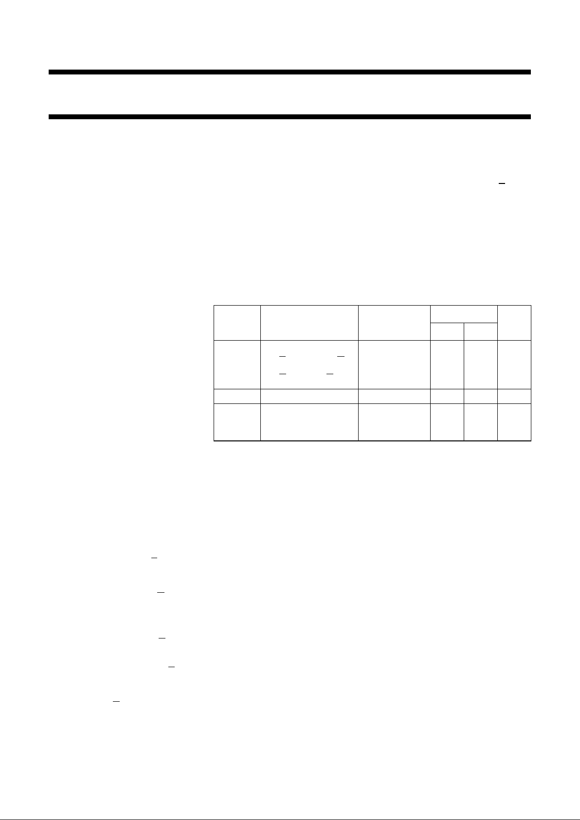
PIN NO. SYMBOL NAME AND FUNCTION
1, 9 1
A, 2A trigger inputs (negative-edge triggered)
2, 10 1B, 2B trigger inputs (positive-edge triggered)
3, 11 1
RD, 2R
D
direct reset LOW and trigger action at positive edge
4, 12 1
Q, 2Q outputs (active LOW)
72R
EXT/CEXT
external resistor/capacitor connection
8 GND ground (0 V)
13, 5 1Q, 2Q outputs (active HIGH)
14, 6 1C
EXT
, 2C
EXT
external capacitor connection
15 1R
EXT/CEXT
external resistor/capacitor connection
16 V
CC
positive supply voltage
Fig.1 Pin configuration. Fig.2 Logic symbol. Fig.3 IEC logic symbol.
1998 Jul 08 4
Philips Semiconductors Product specification
Dual retriggerable monostable
multivibrator with reset
74HC/HCT123
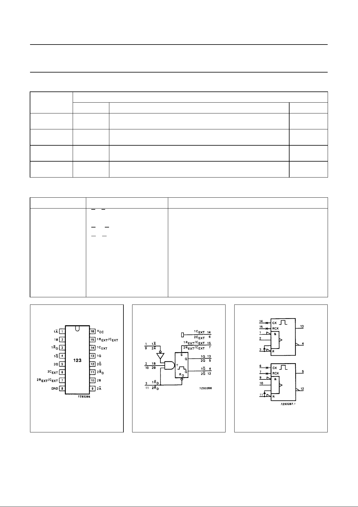
Fig.4 Functional diagram.
FUNCTION TABLE
Note
1. If the monostable was triggered
before this condition was
established, the pulse will
continue as programmed.
INPUTS OUTPUTS
nRDnAnBnQ nQ
LXXL H
XHX L
(1)
H
(1)
XXL L
(1)
H
(1)
HL ↑
H↓ H
↑LH
H = HIGH voltage level
L = LOW voltage level
X = don’t care
↑ = LOW-to-HIGH transition
↓ = HIGH-to-LOW transition
= one HIGH level output pulse
= one LOW level output pulse
Fig.5 Logic diagram.
(1) For minimum noise generation,
it is recommended to ground pins 6 (2C
EXT
)
and 14 (1C
EXT
) externally to pin 8 (GND).
1998 Jul 08 5
Philips Semiconductors Product specification
Dual retriggerable monostable
multivibrator with reset
74HC/HCT123
DC CHARACTERISTICS FOR 74HC
For the DC characteristics see
“74HC/HCT/HCU/HCMOS Logic Family Specifications”
.
Output capability: standard (except for nR
EXT/CEXT
)
ICC category: MSI
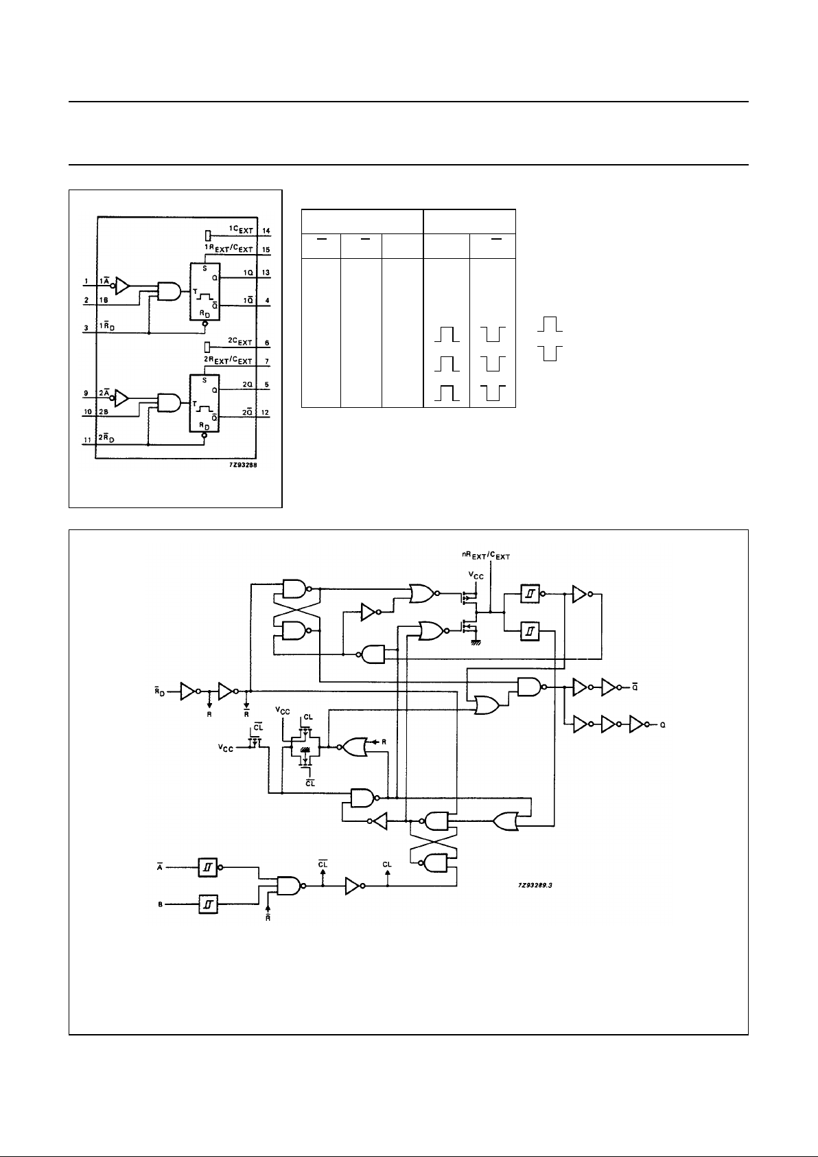
Fig.6 Timing component connections.
1998 Jul 08 6
Philips Semiconductors Product specification
Dual retriggerable monostable
multivibrator with reset
74HC/HCT123
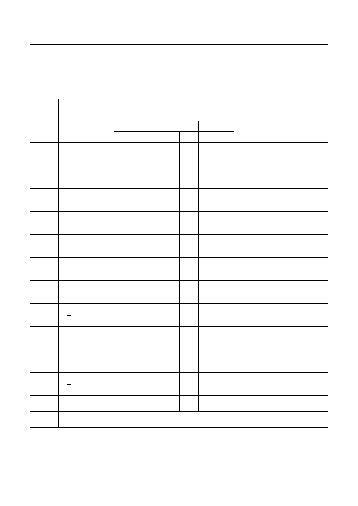
AC CHARACTERISTICS FOR 74HC
GND = 0 V; t
r=tf
= 6 ns; CL=50pF
SYMBOL PARAMETER
T
amb
(°C)
UNIT
TEST CONDITIONS
74HC
V
CC
(V)
WAVEFORMS/
NOTES
+25 −40 to +85 −40 to +125
min. typ. max. min. max. min. max.
t
PLH
propagation delay
nRD, nA, nB to nQ
83
30
24
255
51
43
320
64
54
385
7765ns
2.0
4.5
6.0
C
EXT
= 0 pF;
R
EXT
=5kΩ
t
PLH
propagation delay
nRD, nA, nB to nQ
83
30
24
255
51
43
320
64
54
385
7765ns
2.0
4.5
6.0
C
EXT
= 0 pF;
R
EXT
=5kΩ
t
PHL
propagation delay
nRD to nQ (reset)
66
24
19
215
43
37
270
54
46
325
6555ns
2.0
4.5
6.0
C
EXT
= 0 pF;
R
EXT
=5kΩ
t
PLH
propagation delay
nRD to nQ (reset)
66
24
19
215
43
37
270
54
46
325
6555ns
2.0
4.5
6.0
C
EXT
= 0 pF;
R
EXT
=5kΩ
t
THL
/ t
TLH
output transition
time
19
7
6
75
15
13
95
19
16
110
2219ns
2.0
4.5
6.0
t
W
trigger pulse width
nA = LOW
100
20
17
8
3
2
125
25
21
150
30
26
ns
2.0
4.5
6.0
Fig.7
t
W
trigger pulse width
nB = HIGH
100
20
17
17
6
5
125
25
21
150
30
26
ns
2.0
4.5
6.0
Fig.7
t
W
reset pulse width
nRD= LOW
100
20
17
14
5
4
125
25
21
150
30
26
ns
2.0
4.5
6.0
Fig.8
t
W
output pulse width
nQ = HIGH
nQ = LOW
450 −−µs 5.0
C
EXT
= 100 nF;
R
EXT
=10kΩ;
Figs 7 and 8
t
W
output pulse width
nQ = HIGH
nQ = LOW
75 −−ns 5.0
C
EXT
= 0 pF;
R
EXT
=5kΩ;
note 1; Figs 7 and 8
t
rt
retrigger time
nA, nB
110 −−ns 5.0
C
EXT
= 0 pF;
R
EXT
=5kΩ;
note 2; Fig.7
R
EXT
external timing
resistor
10
2
1000
1000
−−kΩ
2.0
5.0
Fig.9
C
EXT
external timing
capacitor
no limits pF 5.0 Fig.9; note 3
 Loading...