Philips 22HFL3330D/10 Schematic

Colour Television Chassis
TPM1.3HE
LA
I_18120_000.eps
300608
Contents Page Contents Page
1. Technical Specifications, Connections, and Chassis
Overview 2
2. Safety Instructions, Warnings, and Notes 6
3. Directions for Use 7
4. Mechanical Instructions 8
5. Service Modes, Error Codes, and Fault Finding 12
6. Block Diagrams
Wiring Diagram 19" 15
Wiring Diagram 22" 16
SSB of Scaler Board for 19" - 22" 17
7. Circuit Diagrams and PWB Layouts Diagram PWB
3330D/10 SSB: VGA IN/L/R [SB01] 18 37-38
3330D/10 SSB: YPbPr/L/R & SPDIF [SB02] 19 37-38
3330D/10 SSB: S-Video/CVBS/L/R [SB03] 20 37-38
3330D/10 SSB: SCART connector [SB04] 21 37-38
3330D/10 SSB: LVDS OUT [SB05] 22 37-38
3330D/10 SSB: MT5335 HDMI/PLL [SB06] 23 37-38
3330D/10 SSB: MT5335 Control/IR/LED [SB07] 24 37-38
3330D/10 SSB: MT5335 Audio In/Out [SB08] 25 37-38
3330D/10 SSB: DDR1 MEMORY [SB09] 26 37-38
3330D/10 SSB: FLASH/JTAG/UART/IR [SB10] 27 37-38
3330D/10 SSB: CEC uP [SB11] 28 37-38
3330D/10 SSB: HDMI Input Interface [SB12] 29 37-38
3330D/10 SSB: TMDS251 HDMI Switch [SB13] 30 37-38
3330D/10 SSB: LINE OUT/HP [SB14] 31 37-38
3330D/10 SSB: AUDIO AMP CLASS D [SB15] 32 37-38
3330D/10 SSB: EU Tuner Interface [SB16] 33 37-38
3330D/10 SSB: MT5133 ASIC [SB17] 34 37-38
3330D/10 SSB: MT8295/CI CARD [SB18] 35 37-38
3330D/10 SSB: POWER [SB19] 36 37-38
3340D/10 SSB: VGA IN/L/R [SB01] 39 58-59
3340D/10 SSB: YPbPr/L/R & SPDIF [SB02] 40 58-59
3340D/10 SSB: S-Video/CVBS/L/R [SB03] 41 58-59
3340D/10 SSB: SCART connector [SB04] 42 58-59
©
Copyright 2008 Koninklijke Philips Electronics N.V.
All rights reserved. No part of this publication may be reproduced, stored in a
retrieval system or transmitted, in any form or by any means, electronic,
mechanical, photocopying, or otherwise without the prior permission of Philips.
3340D/10 SSB: LVDS OUT [SB05] 43 58-59
3340D/10 SSB: MT5335 HDMI/PLL [SB06] 44 58-59
3340D/10 SSB: MT5335 Control/IR/LED [SB07] 45 58-59
3340D/10 SSB: MT5335 Audio In/Out [SB08] 46 58-59
3340D/10 SSB: DDR1 MEMORY [SB09] 47 58-59
3340D/10 SSB: FLASH/JTAG/UART/IR [SB10] 48 58-59
3340D/10 SSB: CEC uP [SB11] 49 58-59
3340D/10 SSB: HDMI Input Interface [SB12] 50 58-59
3340D/10 SSB: TMDS251 HDMI Switch [SB13] 51 58-59
3340D/10 SSB: LINE OUT/HP [SB14] 52 58-59
3340D/10 SSB: AUDIO AMP CLASS D [SB15] 53 58-59
3340D/10 SSB: EU Tuner Interface [SB16] 54 58-59
3340D/10 SSB: MT5133 ASIC [SB17] 55 58-59
3340D/10 SSB: MT8295/CI CARD [SB18] 56 58-59
3340D/10 SSB: POWER [SB19] 57 58-59
Keyboard & Control Panel [KB01] 60 61
IR & LED Panel [IB01] 62 63
Power Board: Adapter [PB01] 64 66
Power Board: Inverter [PB02] 65 66
8. Alignments 67
9. Circuit Descriptions, Abbreviation List, and IC Data
Sheets 69
10. Spare Parts List & CTN Overview 77
11. Revision List 77
Published by JH 0871 BU TV Consumer Care Printed in the Netherlands Subject to modification EN 3122 785 18121

EN 2 TPM1.3HE LA1.
Technical Specifications, Connections, and Chassis Overview
1. Technical Specifications, Connections, and Chassis Overview
Index of this chapter:
1.1 Technical Specifications
1.2 Connection Overview
1.3 Chassis Overview
Notes:
• Figures can deviate due to the different set executions.
• Specifications are indicative (subject to change).
1.1 Technical Specifications
1.1.1 Vision
Display type : LCD
Screen Size : 19"
Display area (HxV in mm) : 408.2x255.2 (19”)
Number of Pixel (HxV) : 1440x900 (19”)
Pitch (mm) : 0.284x0.284 (19”)
Colour pixel arrangement : RGB vertical stripe
Display operating mode : TN, normally white
Colour depth : 16.7M colours
Brightness (cd/m^2) : 300 (typical)
Viewing angle : R/L 170, U/D 160
Surface treatment : Anti-glare type,
Electrical interface : Dual Channel LVDS
Response time (ms, typical) : 5ms
Contrast ratio (typical) : 1000:1
Backlight : 4 CCFL
Support Video Formats : 720x400@ 70Hz
: 22"
: 473.8x296.1(22”)
: 1680x1050 (22”)
: 0.282x0.282 (22”)
(RGB 6-bits + HiFRC)
Hardness 3H
: 640x480@ 60Hz
: 640x480@ 67Hz
: 800x600@ 60Hz
: 1024x768@ 60Hz
: 1280x960@ 60Hz
: 1440x900@ 60Hz
: 1680x1050@ 60Hz
(22” only)
1.1.2 Sound
Sound systems : Virtual Surround
Maximum power : 2 x 3 W
1.1.3 Miscellaneous
Power supply
AC line voltage range : 90~264 V
AC line frequency range : 50~60 Hz
Power consumption : ~47 W (19”)
: ~55 W (22”)
Scan frequencies
Horizontal : 30~81kHz
Vertical : 56~76 Hz
Product dimension (HxWxD in mm) : 392.3x467.3x69.3mm
Net weight (kg) : 4.4 (19”)
(19”)
: 442.2x533.7x92.3mm
(22”)
: 5.8 (22”)
Technical Specifications, Connections, and Chassis Overview
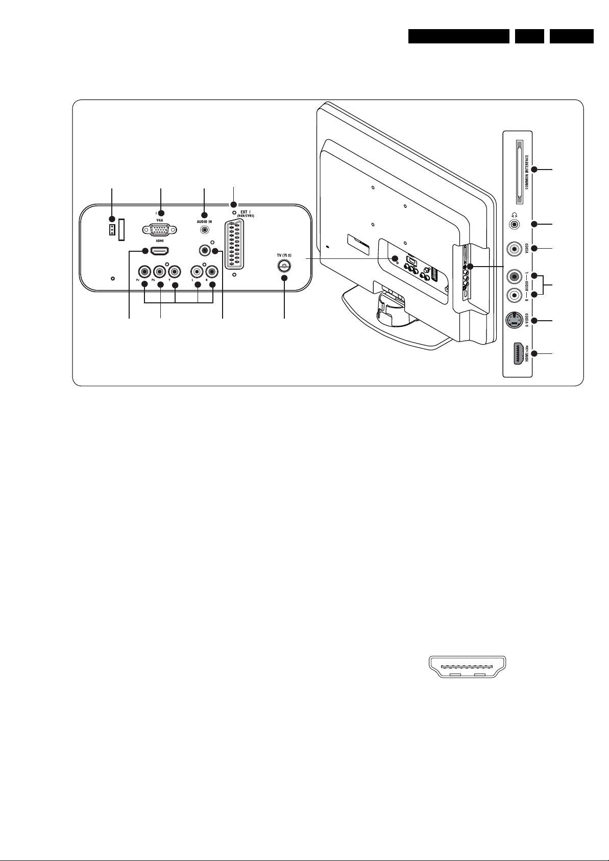
1.2 Connection Overview
14
7
DIGITAL AUDIO OUT
EN 3TPM1.3HE LA 1.
13
16
8
9
EXT 3
Note: The following connector colour abbreviations are used
(acc. to DIN/IEC 757): Bk= Black, Bu= Blue, Gn= Green,
Gy= Grey, Rd= Red, Wh= White, Ye= Yellow.
1.2.1 Rear Connections
1. EXT1: Video RGB/CVBS - In, CVBS - out, Audio - In
4 5 3 2
Figure 1-1 Connection overview
17 - Ground Video Gnd H
18 - Ground FBL Gnd H
19 - Video CVBS 1 V
20 - Video CVBS 1 V
21 - Shield Gnd H
2. EXT3 Cinch: Video YPbPr - In, Audio - In
Gn - Video Y 1 V
Bu - Video Pb 0.7 V
Rd - Video Pr 0.7 V
Wh - Audio L 0.5 V
Rd - Audio R 0.5 V
3. Cinch: S/PDIF - Out
Bk - Coaxial 0.4 - 0.6V
10
11
12
I_18120_055.eps
/ 75 ohm k
PP
/ 75 ohm j
PP
/ 75 ohm jq
PP
/ 75 ohm jq
PP
/ 75 ohm jq
PP
/ 10 kohm jq
RMS
/ 10 kohm jq
RMS
/ 75 ohm kq
PP
140808
Figure 1-2 SCART connector
1-n.c.
2 -Audio R 0.5 V
3-n.c.
4 -Ground Audio Gnd H
5 -Ground Blue Gnd H
6 -Audio L 0.5 V
7 -Video Blue 0.7 V
8 -Function Select 0 - 2 V: INT
4.5 - 7 V: EXT 16:9
9.5 - 12 V: EXT 4:3 j
9 - Ground Green Gnd H
10 - n.c.
11 - Video Green 0.7 V
12 - n.c.
13 - Ground Red Gnd H
14 - Ground Data Gnd H
15 - Video Red 0.7 V
16 - Status/FBL 0 - 0.4 V: INT
1 - 3 V: EXT / 75 ohm j
/ 10 kohm j
RMS
/ 10 kohm j
RMS
/ 75 ohm j
PP
/ 75 ohm j
PP
/ 75 ohm j
PP
4. Aerial - In
- - IEC-type (EU) Coax, 75 ohm D
5. HDMI: Digital Video, Digital Audio - In
19
18 2
Figure 1-3 HDMI (type A) connector
1 - D2+ Data channel j
2 - Shield Gnd H
3 - D2- Data channel j
4 - D1+ Data channel j
5 - Shield Gnd H
6 - D1- Data channel j
7 - D0+ Data channel j
8 - Shield Gnd H
9 - D0- Data channel j
10 - CLK+ Data channel j
1
E_06532_017.eps
250505

EN 4 TPM1.3HE LA1.
Technical Specifications, Connections, and Chassis Overview
11 - Shield Gnd H
12 - CLK- Data channel j
13 - Easylink Control channel jk
14 - n.c.
15 - DDC_SCL DDC clock j
16 - DDC_SDA DDC data jk
17 - Ground Gnd H
18 - +5V j
19 - HPD Hot Plug Detect j
20 - Ground Gnd H
6. Mini Jack: Audio - In
Wh - Audio L 0.5 V
Rd - Audio R 0.5 V
/ 10 kohm jo
RMS
/ 10 kohm jo
RMS
7. VGA: Video RGB - In
1
5
6
11
10
15
E_06532_002.eps
050404
Figure 1-4 VGA Connector
1 - Video Red 0.7 V
2 - Video Green 0.7 V
3 - Video Blue 0.7 V
4-n.c.
/ 75 ohm j
PP
/ 75 ohm j
PP
/ 75 ohm j
PP
5 - Ground Gnd H
6 - Ground Red Gnd H
7 - Ground Green Gnd H
8 - Ground Blue Gnd H
9-+5V
10 - Ground Sync Gnd H
+5 V j
DC
11 - n.c.
12 - DDC_SDA DDC data j
13 - H-sync 0 - 5 V j
14 - V-sync 0 - 5 V j
15 - DDC_SCL DDC clock j
8 - Shield Gnd H
9 - D0- Data channel j
10 - CLK+ Data channel j
11 - Shield Gnd H
12 - CLK- Data channel j
13 - Easylink Control channel jk
14 - n.c.
15 - DDC_SCL DDC clock j
16 - DDC_SDA DDC data jk
17 - Ground Gnd H
18 - +5V j
19 - HPD Hot Plug Detect j
20 - Ground Gnd H
13. Common Interface
68p - See diagram SB18 jk
14. Service Connector (UART)
1 - UART_TX Transmit k
2 - Ground Gnd H
3 - UART_RX Receive j
1.2.2 Side Connections
8. Mini Jack: Audio Head phone - Out
Bk - Head phone 32 - 600 ohm / 10 mW ot
9. EXT2 Cinch: Video CVBS - In
Ye - Video CVBS 1 V
/ 75 ohm jq
PP
10. EXT2 Cinch: Audio - In
Wh - Audio L 0.5 V
Rd - Audio R 0.5 V
/ 10 kohm jq
RMS
/ 10 kohm jq
RMS
11. EXT2 S-Video (Hosiden): Video Y/C - In
1 - Ground Y Gnd H
2 - Ground C Gnd H
3 - Video Y 1 V
4 - Video C 0.3 V
/ 75 ohm j
PP
P / 75 ohm j
PP
12. HDMI: Digital Video, Digital Audio - In
19
18 2
1
E_06532_017.eps
250505
Figure 1-5 HDMI (type A) connector
1 - D2+ Data channel j
2-Shield Gnd H
3 - D2- Data channel j
4 - D1+ Data channel j
5-Shield Gnd H
6 - D1- Data channel j
7 - D0+ Data channel j
Technical Specifications, Connections, and Chassis Overview
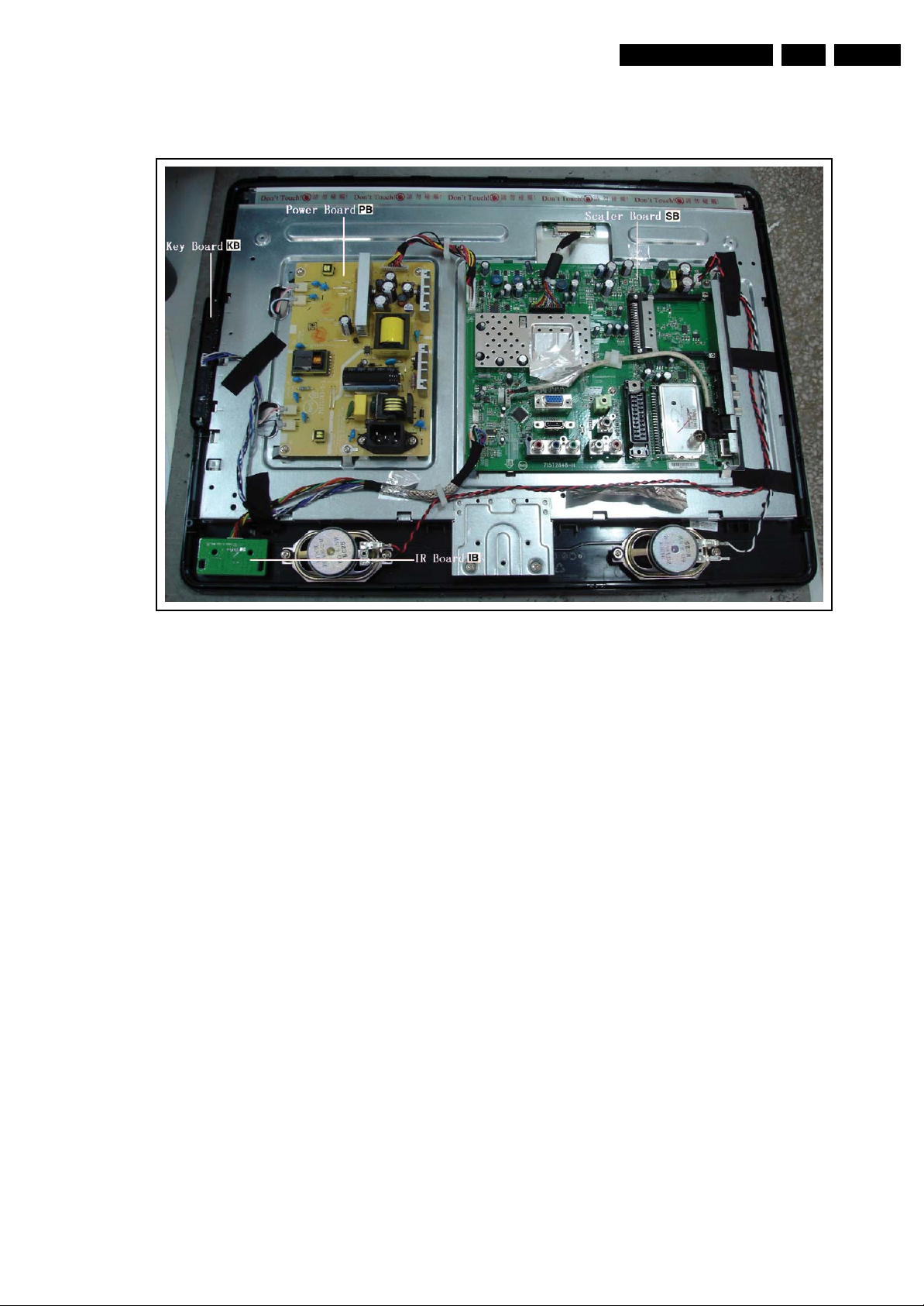
1.3 Chassis Overview
EN 5TPM1.3HE LA 1.
Figure 1-6 Chassis Overview 19” & 22”
I_18120_001.eps
250608

EN 6 TPM1.3HE LA2.
Safety Instructions, Warnings, and Notes
2. Safety Instructions, Warnings, and Notes
Index of this chapter:
2.1 Safety Instructions
2.2 Warnings
2.3 Notes
2.1 Safety Instructions
Safety regulations require the following during a repair:
• Connect the set to the Mains/AC Power via an isolation
transformer (> 800 VA).
• Replace safety components, indicated by the symbol h,
only by components identical to the original ones. Any
other component substitution (other than original type) may
increase risk of fire or electrical shock hazard.
Safety regulations require that after a repair, the set must be
returned in its original condition. Pay in particular attention to
the following points:
• Route the wire trees correctly and fix them with the
mounted cable clamps.
• Check the insulation of the Mains/AC Power lead for
external damage.
• Check the strain relief of the Mains/AC Power cord for
proper function.
• Check the electrical DC resistance between the Mains/AC
Power plug and the secondary side (only for sets that have
a Mains/AC Power isolated power supply):
1. Unplug the Mains/AC Power cord and connect a wire
between the two pins of the Mains/AC Power plug.
2. Set the Mains/AC Power switch to the “on” position
(keep the Mains/AC Power cord unplugged!).
3. Measure the resistance value between the pins of the
Mains/AC Power plug and the metal shielding of the
tuner or the aerial connection on the set. The reading
should be between 4.5 MΩ and 12 MΩ.
4. Switch “off” the set, and remove the wire between the
two pins of the Mains/AC Power plug.
• Check the cabinet for defects, to prevent touching of any
inner parts by the customer.
2.2 Warnings
• All ICs and many other semiconductors are susceptible to
electrostatic discharges (ESD w). Careless handling
during repair can reduce life drastically. Make sure that,
during repair, you are connected with the same potential as
the mass of the set by a wristband with resistance. Keep
components and tools also at this same potential.
• Be careful during measurements in the high voltage
section.
• Never replace modules or other components while the unit
is switched “on”.
• When you align the set, use plastic rather than metal tools.
This will prevent any short circuits and the danger of a
circuit becoming unstable.
2.3 Notes
2.3.1 General
• Measure the voltages and waveforms with regard to the
chassis (= tuner) ground (H), or hot ground (I), depending
on the tested area of circuitry. The voltages and waveforms
shown in the diagrams are indicative. Measure them in the
Service Default Mode (see chapter 5) with a colour bar
signal and stereo sound (L: 3 kHz, R: 1 kHz unless stated
otherwise) and picture carrier at 475.25 MHz for PAL, or
61.25 MHz for NTSC (channel 3).
• Where necessary, measure the waveforms and voltages
with (D) and without (E) aerial signal. Measure the
voltages in the power supply section both in normal
operation (G) and in stand-by (F). These values are
indicated by means of the appropriate symbols.
• Manufactured under license from Dolby Laboratories.
“Dolby”, “Pro Logic” and the “double-D symbol”, are
trademarks of Dolby Laboratories.
2.3.2 Schematic Notes
• All resistor values are in ohms, and the value multiplier is
often used to indicate the decimal point location (e.g. 2K2
indicates 2.2 kΩ).
• Resistor values with no multiplier may be indicated with
either an “E” or an “R” (e.g. 220E or 220R indicates 220 Ω).
• All capacitor values are given in micro-farads (μ=× 10
nano-farads (n =× 10
• Capacitor values may also use the value multiplier as the
decimal point indication (e.g. 2p2 indicates 2.2 pF).
• An “asterisk” (*) indicates component usage varies. Refer
to the diversity tables for the correct values.
• The correct component values are listed in the Spare Parts
List. Therefore, always check this list when there is any
doubt.
2.3.3 BGA (Ball Grid Array) ICs
Introduction
For more information on how to handle BGA devices, visit this
URL: www.atyourservice.ce.philips.com (needs subscription,
not available for all regions). After login, select “Magazine”,
then go to “Repair downloads”. Here you will find Information
on how to deal with BGA-ICs.
BGA Temperature Profiles
For BGA-ICs, you must use the correct temperature-profile,
which is coupled to the 12NC. For an overview of these profiles,
visit the website www.atyourservice.ce.philips.com (needs
subscription, but is not available for all regions)
You will find this and more technical information within the
“Magazine”, chapter “Repair downloads”.
For additional questions please contact your local repair help
desk.
2.3.4 Lead-free Soldering
Due to lead-free technology some rules have to be respected
by the workshop during a repair:
• Use only lead-free soldering tin Philips SAC305 with order
code 0622 149 00106. If lead-free solder paste is required,
please contact the manufacturer of your soldering
equipment. In general, use of solder paste within
workshops should be avoided because paste is not easy to
store and to handle.
• Use only adequate solder tools applicable for lead-free
soldering tin. The solder tool must be able:
– To reach a solder-tip temperature of at least 400°C.
– To stabilize the adjusted temperature at the solder-tip.
– To exchange solder-tips for different applications.
• Adjust your solder tool so that a temperature of around
360°C - 380°C is reached and stabilized at the solder joint.
Heating time of the solder-joint should not exceed ~ 4 sec.
Avoid temperatures above 400°C, otherwise wear-out of
tips will increase drastically and flux-fluid will be destroyed.
To avoid wear-out of tips, switch “off” unused equipment or
reduce heat.
• Mix of lead-free soldering tin/parts with leaded soldering
tin/parts is possible but PHILIPS recommends strongly to
-9
), or pico-farads (p =× 10
-12
-6
),
).

Directions for Use
EN 7TPM1.3HE LA 3.
avoid mixed regimes. If this cannot be avoided, carefully
clear the solder-joint from old tin and re-solder with new tin.
2.3.5 Alternative BOM identification
It should be noted that on the European Service website,
“Alternative BOM” is referred to as “Design variant”.
The third digit in the serial number (example:
AG2B0335000001) indicates the number of the alternative
B.O.M. (Bill Of Materials) that has been used for producing the
specific TV set. In general, it is possible that the same TV
model on the market is produced with e.g. two different types
of displays, coming from two different suppliers. This will then
result in sets which have the same CTN (Commercial Type
Number; e.g. 28PW9515/12) but which have a different B.O.M.
number.
By looking at the third digit of the serial number, one can
identify which B.O.M. is used for the TV set he is working with.
If the third digit of the serial number contains the number “1”
(example: AG1B033500001), then the TV set has been
manufactured according to B.O.M. number 1. If the third digit is
a “2” (example: AG2B0335000001), then the set has been
produced according to B.O.M. no. 2. This is important for
ordering the correct spare parts!
For the third digit, the numbers 1...9 and the characters A...Z
can be used, so in total: 9 plus 26= 35 different B.O.M.s can be
indicated by the third digit of the serial number.
Identification: The bottom line of a type plate gives a 14-digit
serial number. Digits 1 and 2 refer to the production centre (e.g.
AG is Bruges), digit 3 refers to the B.O.M. code, digit 4 refers
to the Service version change code, digits 5 and 6 refer to the
production year, and digits 7 and 8 refer to production week
(in example below it is 2006 week 17). The 6 last digits contain
the serial number.
MODEL :
PROD.NO:
32PF9968/10
AG 1A0617 000001
MADE IN BELGIUM
220-240V 50/60Hz
~
VHF+S+H+UHF
S
128W
BJ3.0E LA
E_06532_024.eps
260308
Figure 2-1 Serial number (example)
2.3.6 Board Level Repair (BLR) or Component Level Repair
(CLR)
If a board is defective, consult your repair procedure to decide
if the board has to be exchanged or if it should be repaired on
component level.
If your repair procedure says the board should be exchanged
completely, do not solder on the defective board. Otherwise, it
cannot be returned to the O.E.M. supplier for back charging!
2.3.7 Practical Service Precautions
• It makes sense to avoid exposure to electrical shock.
While some sources are expected to have a possible
dangerous impact, others of quite high potential are of
limited current and are sometimes held in less regard.
• Always respect voltages. While some may not be
dangerous in themselves, they can cause unexpected
reactions that are best avoided. Before reaching into a
powered TV set, it is best to test the high voltage insulation.
It is easy to do, and is a good service precaution.
3. Directions for Use
You can download this information from the following websites:
http://www.philips.com/support
http://www.p4c.philips.com
EN 8 TPM1.3HE LA4.
Mechanical Instructions
4. Mechanical Instructions
Index of this chapter:
4.1 Cable Dressing
4.2 Service Positions
4.3 Assy/Panel Removal
4.4 Set Re-assembly
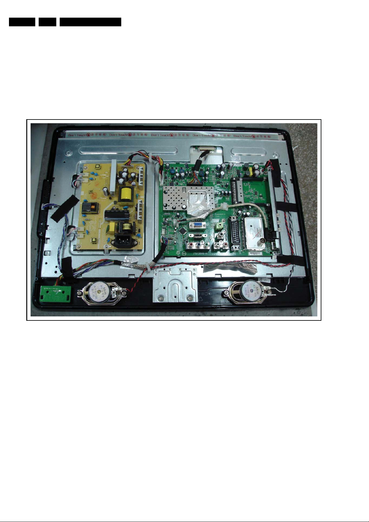
4.1 Cable Dressing
Figure 4-1 Cable dressing (19HFL3330D/10 & 19HFL3340D/10 & 22HFL3330D/10)
I_18120_002.eps
250608
Mechanical Instructions
EN 9TPM1.3HE LA 4.
4.2 Service Positions
For easy servicing of this set, there are a few possibilities
created:
• The buffers from the packaging (see figure “Rear cover”).
• Foam bars (created for Service).
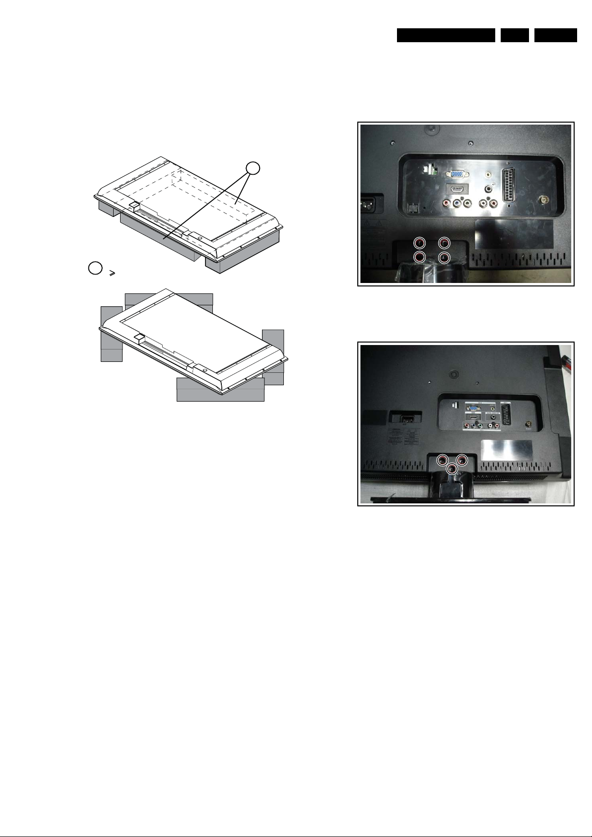
4.2.1 Foam Bars
Required for sets
1
42"
4.3 Assy/Panel Removal
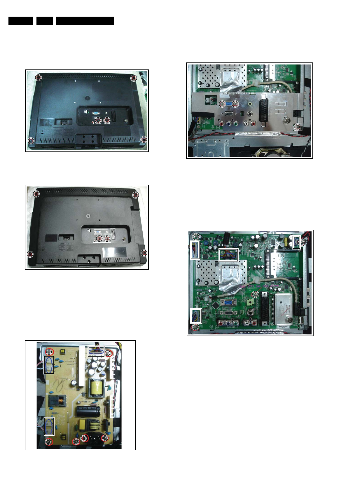
4.3.1 Stand
Remove the marked screws to remove the stand.
1
I_18120_003.eps
250608
Figure 4-3 Remove stand (19”)
E_06532_018.eps
171106
Figure 4-2 Foam bars
The foam bars (order code 3122 785 90580 for two pieces) can
be used for all types and sizes of Flat TVs. See figure “Foam
bars” for details. Sets with a display of 42” and larger, require
four foam bars [1]. Ensure that the foam bars are always
supporting the cabinet and never only the display.
Caution: Failure to follow these guidelines can seriously
damage the display!
By laying the TV face down on the (ESD protective) foam bars,
a stable situation is created to perform measurements and
alignments. By placing a mirror under the TV, you can monitor
the screen.
Figure 4-4 Remove stand (22”)
I_18120_004.eps
250608
EN 10 TPM1.3HE LA4.
Mechanical Instructions
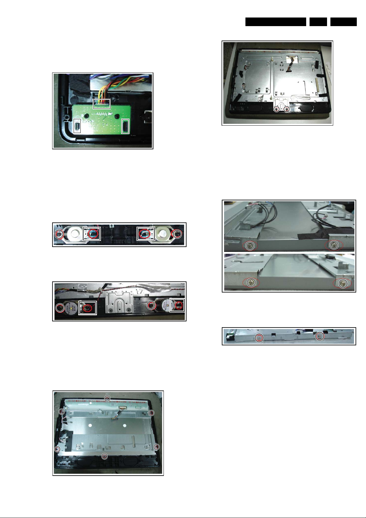
4.3.2 Rear Cover
1. Remove the marked screws, which secure the rear cover.
2. Lift the rear cover from the cabinet. Make sure that wires
and flat foils are not damaged during cover removal.
Figure 4-5 Remove rear cover (19”)
I_18120_005.eps
250608
4.3.4 Shielding EMI
1. Refer to next figure.
2. Release the marked screws and remove the shielding-EMI.
Figure 4-8 Shielding-EMI
4.3.5 Scaler Board
1. Refer to next figure.
2. Unplug marked connectors.
3. Release marked screws and remove the scaler board.
When defective, replace the whole unit.
I_18120_008.eps
250608
Figure 4-6 Remove rear cover (22”)
4.3.3 Power Board
1. Refer to next figure.
2. Unplug marked connectors.
3. Release marked screws and remove the power board.
When defective, replace the whole unit.
I_18120_006.eps
250608
22” sets only
Figure 4-9 Scaler Board
I_18120_009.eps
250608
Figure 4-7 Power Board
I_18120_007.eps
250608
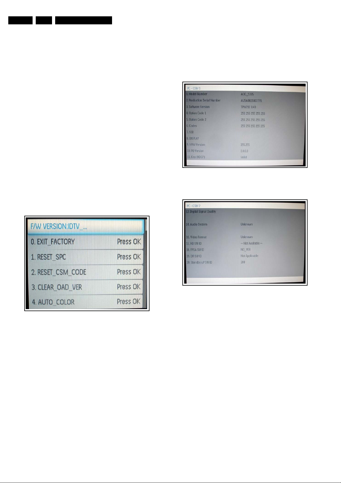
4.3.6 IR Board
1. Refer to next figure
2. Unplug the marked connector.
When defective, replace the whole unit.
Figure 4-10 IR Board
4.3.7 Speakers
1. Refer to next figures.
2. Unplug marked connectors.
3. Remove the marked screws.
Remove the speaker.
I_18120_010.eps
250608
Mechanical Instructions
4.3.9 Bracket, Main Frame and LCD Panel
1. Refer to next two figures.
2. Remove the marked screws.
3. Remove the bracket/frame.
4. Lift the LCD panel from the set.
Figure 4-14 Bezel (22”)
I_18120_014.eps
250608
EN 11TPM1.3HE LA 4.
Figure 4-11 Speakers (19”)
Figure 4-12 Speakers (22”)
4.3.8 Bezel
1. Refer to next figures.
2. Remove the marked screws.
Remove the bezel.
I_18120_011.eps
250608
I_18120_012.eps
250608
Figure 4-15 Bracket (19”)
Figure 4-16 Main Frame (22”)
4.4 Set Re-assembly
To re-assemble the whole set, execute all processes in reverse
order.
Notes:
• While re-assembling, make sure that all cables are placed
and connected in their original position. See figure “Cable
dressing”.
I_18120_015.eps
250608
I_18120_016.eps
250608
Figure 4-13 Bezel (19”)
I_18120_013.eps
250608
EN 12 TPM1.3HE LA5.
Service Modes, Error Codes, and Fault Finding
5. Service Modes, Error Codes, and Fault Finding
Index of this chapter:
5.1 Test Points
5.2 Service Mode
5.3 Error Codes
5.4 Service Tools
5.1 Test Points
This chassis is not equipped with test points in the service
printing. These test points are not specifically mentioned in the
service manual
5.2 Service Mode
5.2.1 Factory Mode or Service Alignment Mode (SAM)
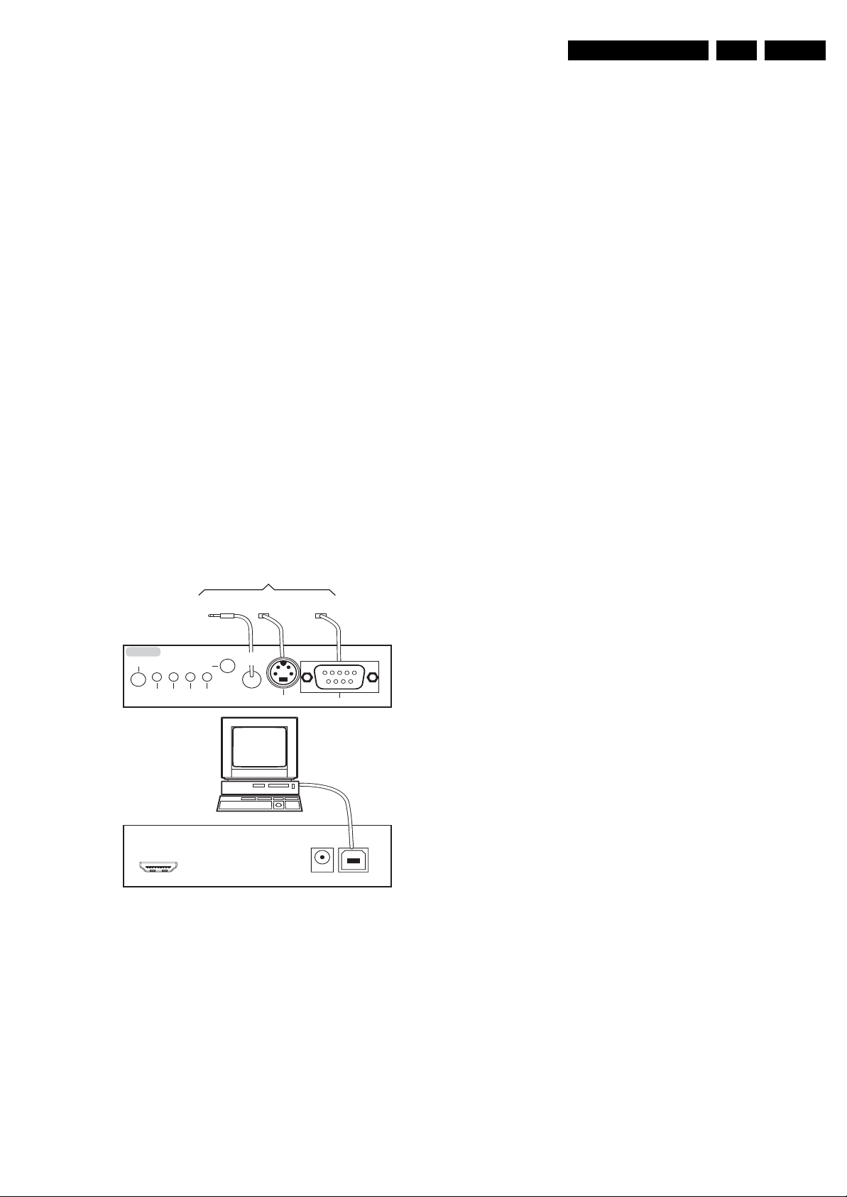
How to Enter
To enter the Factory mode, use the following method:
• Press on the remote control the code “062596” directly
followed by the “INFO” key.
• Press the “MENU” key and select “FACTORY” and press
“OK” to enter the “Factory” mode as shown in the next
picture.
Caution: This function is available for development and
service personnel only, not for end customers.
How to Navigate
By means of the “CURSOR-DOWN/UP” knob on the RCtransmitter on the screen.
Contents of CSM
I_18120_018.eps
Figure 5-2 CSM Menu 1
250608
Figure 5-1 Factory mode menu
How to EXIT
Select "EXIT_FACTORY" and press "OK" bottom on remote
control.
5.2.2 Customer Service Mode (CSM)
Purpose
When a customer is having problems with his TV-set, he can
call his dealer or the Customer Help desk. The service
technician can then ask the customer to activate the CSM, in
order to identify the status of the set. Now, the service
technician can judge the severity of the complaint. In many
cases, he can advise the customer how to solve the problem,
or he can decide if it is necessary to visit the customer. The
CSM is a read only mode; therefore, modifications in this mode
are not possible.
How to Activate CSM
Key in the code ”123654” via the standard RC transmitter.
I_18120_017.eps
250608
I_18120_019.eps
250608
Figure 5-3 CSM Menu 2
Menu Explanation
1. Model Number: AOC_5335
2. Production Serial Number: Product serial no.
3. Software Version
4. Option Code 1: Option codes group 1.
5. Option Code 2: Option codes group 2.
6. Codes: Error buffer contents
7. SSB: Order code of the SSB
8. DISPLAY: Type nr./order code of display.
9. NVM Version: The version of EEPROM.
10. PQ Version: The version of Picture Quality SW.
11. Key (HDCP): Indicates if the HDCP-keys are valid (HDMI).
12. Digital Signal Quality: Indicates the signal quality.
13. N.a.
14. Audio System: Indicates the received audio system.
15. N.a.
16. Video Format: Indicates the received video format.
17. HD SW ID: Version indication of the used SW.
18. FPGA SW ID: Version indication of the used SW.
19. DFI SW ID: Version indication of the used SW.
20. Stand-by uP SW ID: Version indication of the used SW.
How to exit
Press "MENU" on the RC-transmitter.
Service Modes, Error Codes, and Fault Finding
EN 13TPM1.3HE LA 5.
5.3 Error Codes
Not available at the time of publishing.
5.4 Service Tools
5.4.1 ComPair
Introduction
ComPair (Computer Aided Repair) is a Service tool for Philips
Consumer Electronics products. And offers the following:
1. ComPair helps you to quickly get an understanding on how
to repair the chassis in a short and effective way.
2. ComPair allows very detailed diagnostics and is therefore
capable of accurately indicating problem areas. You do not
have to know anything about I
yourself, because ComPair takes care of this.
3. ComPair speeds up the repair time since it can
automatically communicate with the chassis (when the uP
is working) and all repair information is directly available.
4. ComPair features TV software upgrade possibilities.
Specifications
ComPair consists of a Windows based fault finding program
and an interface box between PC and the (defective) product.
The (new) ComPair II interface box is connected to the PC via
a USB cable. For the TV chassis, the ComPair interface box
and the TV communicate via a bi-directional cable via the
service connector(s).
2
C or UART commands
Note: If you encounter any problems, contact your local
support desk.
How to Connect
This is described in the ComPair chassis fault finding database.
TO TV
UART SERVICE
CONNECTOR
2
I
C
TO
RS232 /UART
ComPair II
RC in
Optional
Switch
Power ModeLink/
Activity
UART SERVICE
CONNECTOR
RC out
TO
TO
I2C SERVICE
CONNECTOR
Multi
function
PC
ComPair II Developed by Philips Brugge
Optional power
HDMI
2
I
C only
5V DC
E_06532_036.eps
150208
Figure 5-4 ComPair II interface connection
Caution: It is compulsory to connect the TV to the PC as
shown in the picture above (with the ComPair interface in
between), as the ComPair interface acts as a level shifter. If
one connects the TV directly to the PC (via UART), ICs will be
blown!
How to Order
ComPair II order codes:
• ComPair II interface: 3122 785 91020.
• For latest software see Philips Service website.
• ComPair UART interface cable: 3122 785 90630.

EN 14 TPM1.3HE LA5.
Personal Notes:
Service Modes, Error Codes, and Fault Finding
E_06532_012.eps
131004
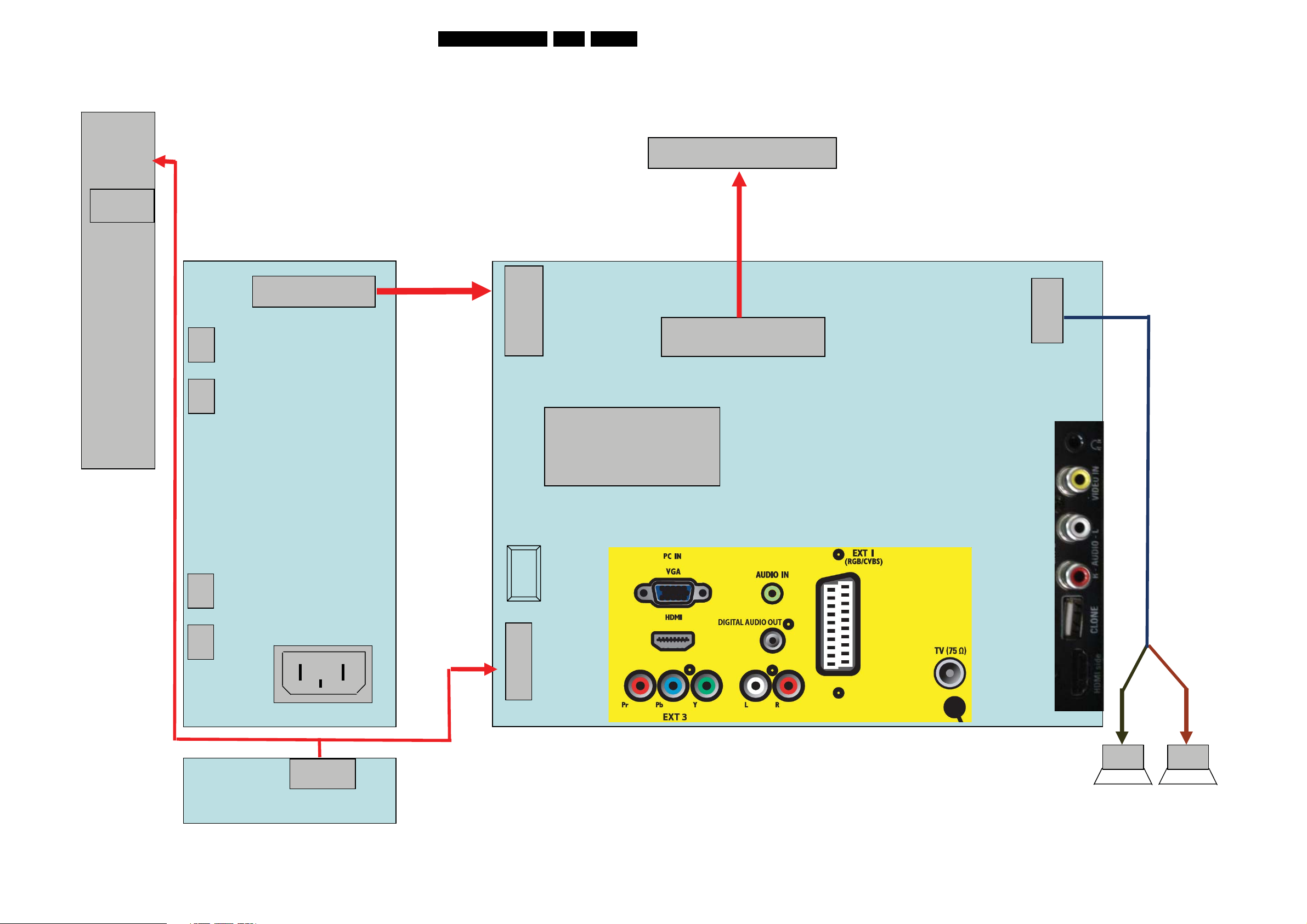
6. Block Diagrams
Wiring Diagram 19"
Block Diagrams
15TPM1.3HE LA 6.
Key
Board
5 Pin
CN101
Panel
5
1
095T8018 3DH36 LVDS Cable
11
11 Pin
CN902
CN802
CN801
1
095T 82011X511
WIRE HARNESS
12
CN902
12 Pin
1
1
MT5335PGU
U401
30 Pin
CN301
30
4 Pin
CN602
Head Phone
4
1
WIRE HARNESS
095T8014 4X565
Power Board
CN804
CN803
IR Board
AC IN
CN901
1
6 Pin
CN1
Scaler IC
Main Board
VIDEO
AUDIO R/L
095T801411X510
11
CLONE
11Pin
WIRE HARNESS
CN404
HDMI
1
6
Speaker R/L
I_18120_051.eps
270608
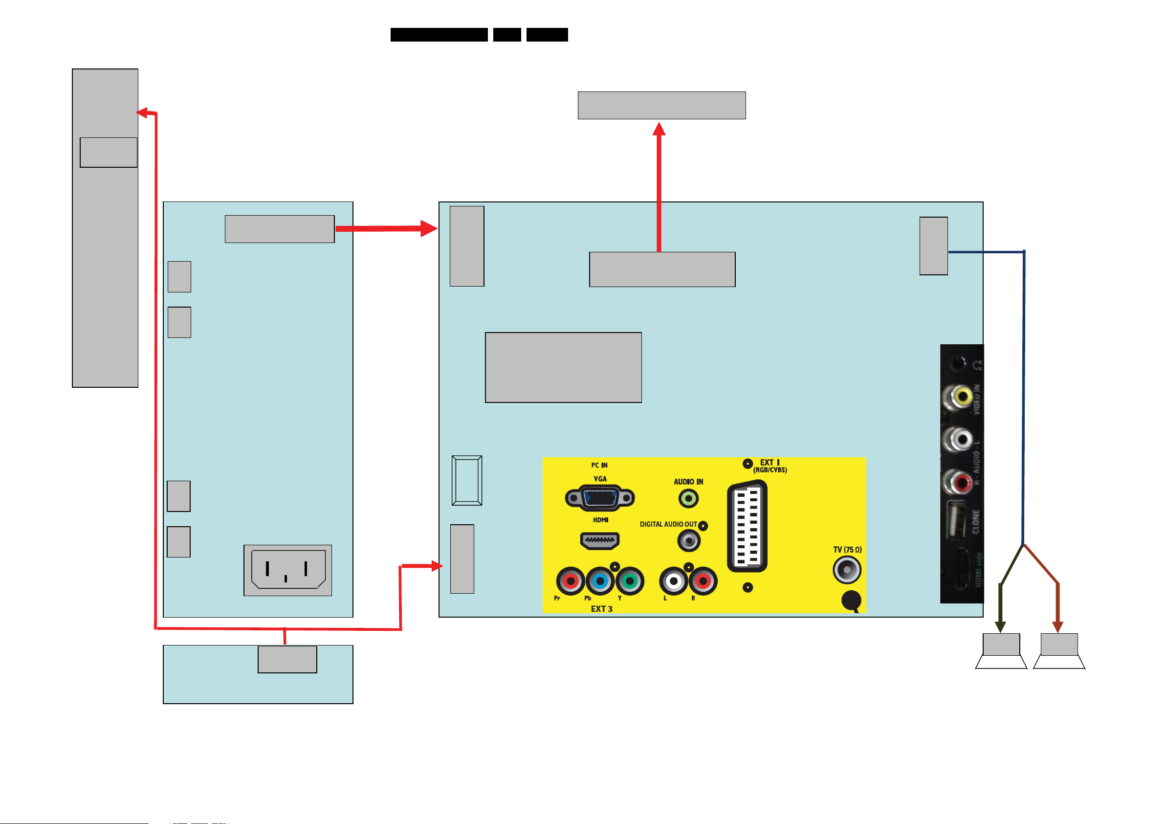
Wiring Diagram 22"
Block Diagrams
16TPM1.3HE LA 6.
Key
Board
5 Pin
CN101
Panel
5
1
095T8018 3XH36 LVDS Cable
11
11 Pin
CN902
CN802
CN801
1
095T 82011X503
WIRE HARNESS
12
CN902
12 Pin
1
1
MT5335PGU
U401
30 Pin
CN301
30
4 Pin
CN602
Head Phone
4
1
WIRE HARNESS
095T8014 4D553
Power Board
CN804
CN803
IR Board
AC IN
CN901
1
6 Pin
CN1
Scaler IC
Main Board
VIDEO
AUDIO R/L
095T801411D509
11
CLONE
11Pin
WIRE HARNESS
CN404
HDMI
1
6
Speaker R/L
I_18120_052.eps
270608
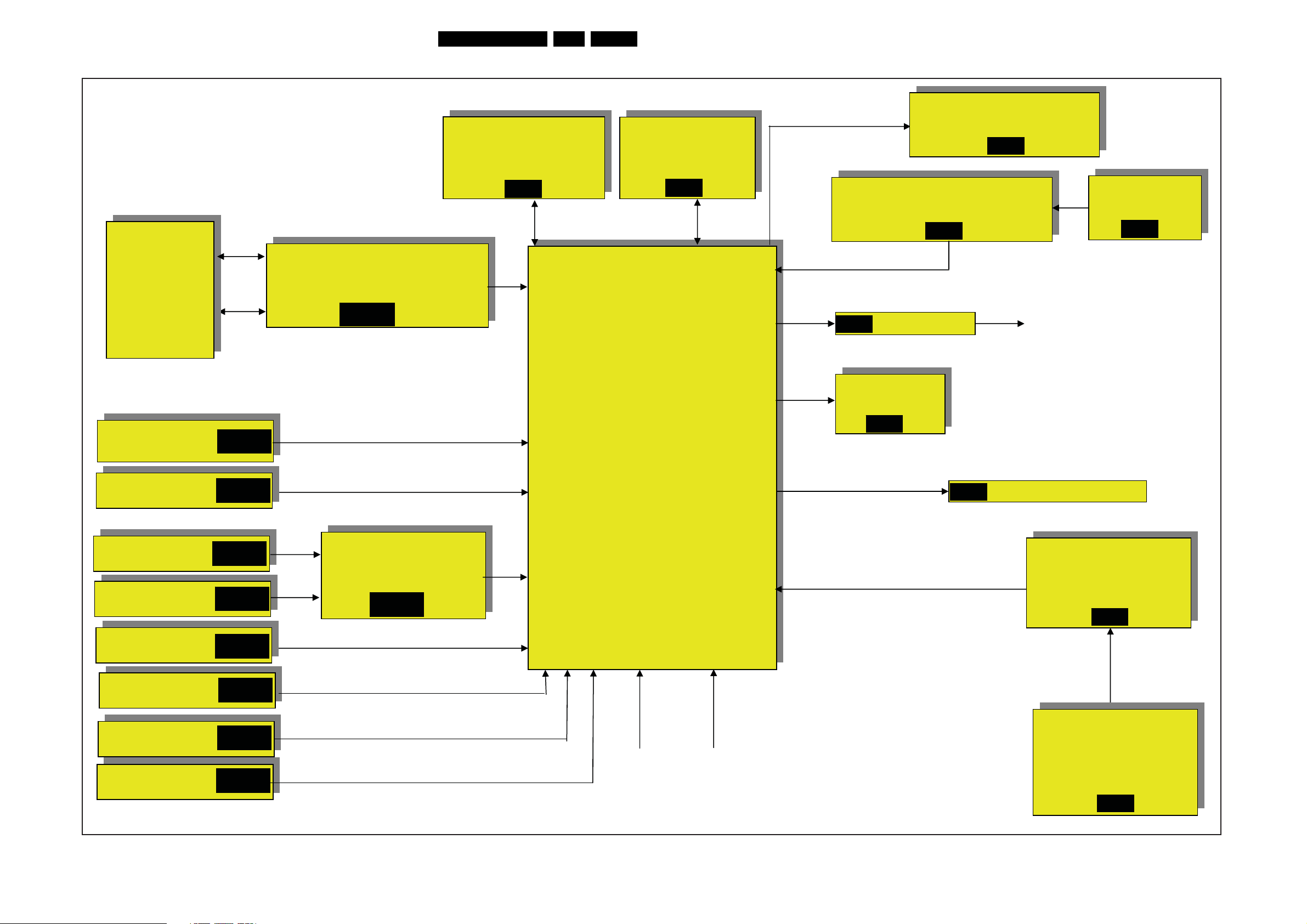
SSB of Scaler Board for 19" - 22"
Power
16V
Board
Block Diagrams
Power
3.3V,2.5V,1.8V,1.2V,1.1V
DDR SDRAM
HY5DU121622DTP-D43
2.5V
SB-09
MT5335PGU
17TPM1.3HE LA 6.
Sub MCU
WT6702F_OG200WT
3.3V
SB-11
Audio AMP
TDA8932BTW
12V
SB-15
Common Interface Controller
MT8295
3.3V,1.8V
SB-18
PCMCIA
5V,3.3V
SB-18
D-SUB/PC-VGA
SCART
HDMI 1
HDMI 2
5V
SB-01
SB-04
SB-13
SB-13
SB-19
HDMI MUX
TMDS251PAGR
5V,3.3V
SB-13
MPEG-1 layer I/II decoding
Audio ADC
Audio DAC
3D surround processing with
Virtual surround
Automatic volume control
Audio I/F
2-D Graphic
De-interlace
VADCx4
HDMI In I/F
Digital TV Demodulator
Analog TV IF Demodulator
TV audio demodulator
USB2.0
3.3V,2.5V,1.2V,1.1V
SB-14
SPIDF OUT
2.5V
SB-18
EARPHONE AMP
SB-10
Headphone
Flash MX25L3205DMI-12G
Channel demodulator
MT5133
3.3V
SB-17
YPbPr/L/R
Audio R/L of CVBS
Audio R/L of PC
USB Port
SB-02
SB-03
SB-01
SB-10
IR
Keypad
TUNER
ENG37E14KF
5V
SB-17
I_18120_053.eps
270608
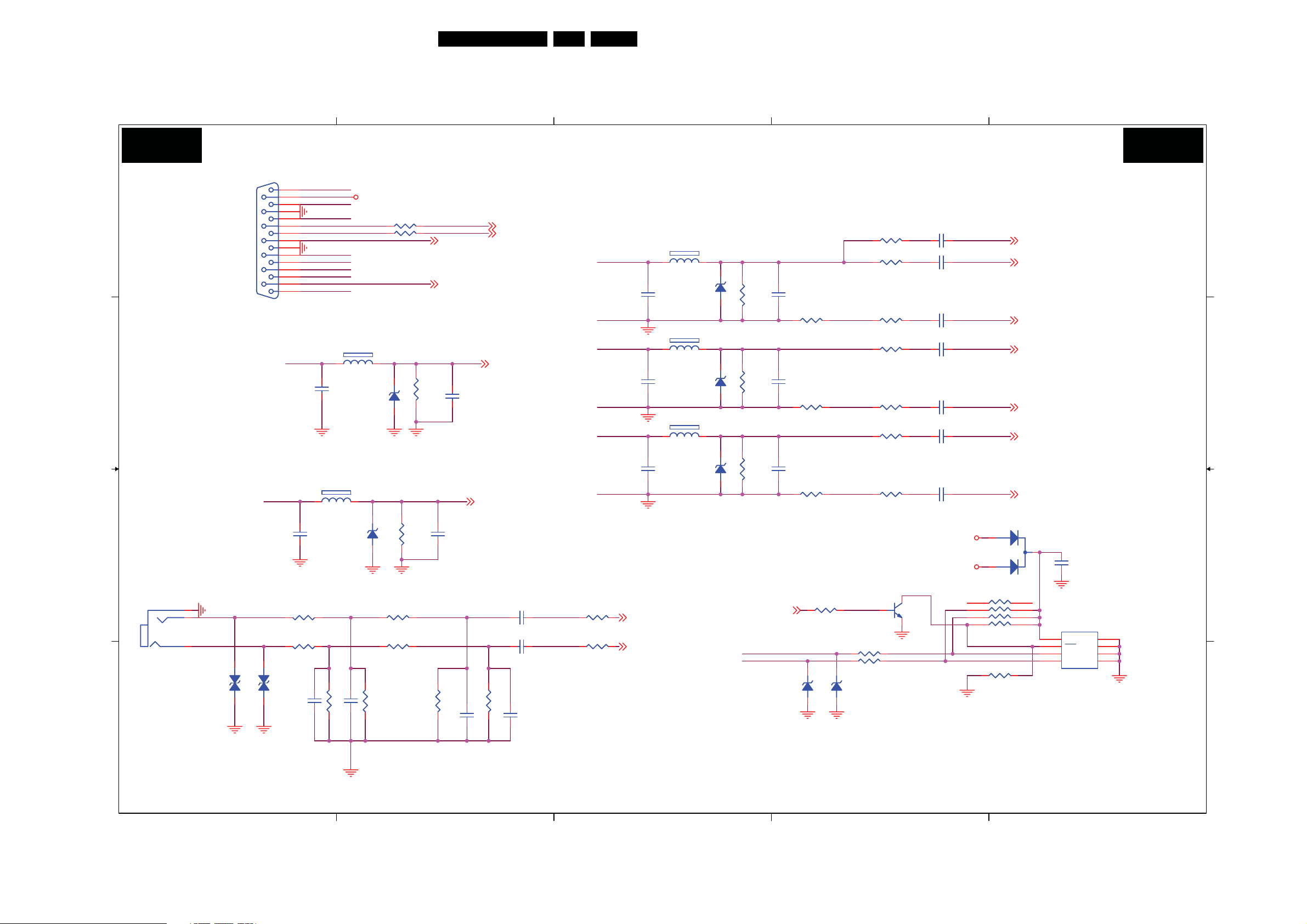
Circuit Diagrams and PWB Layouts
7. Circuit Diagrams and PWB Layouts
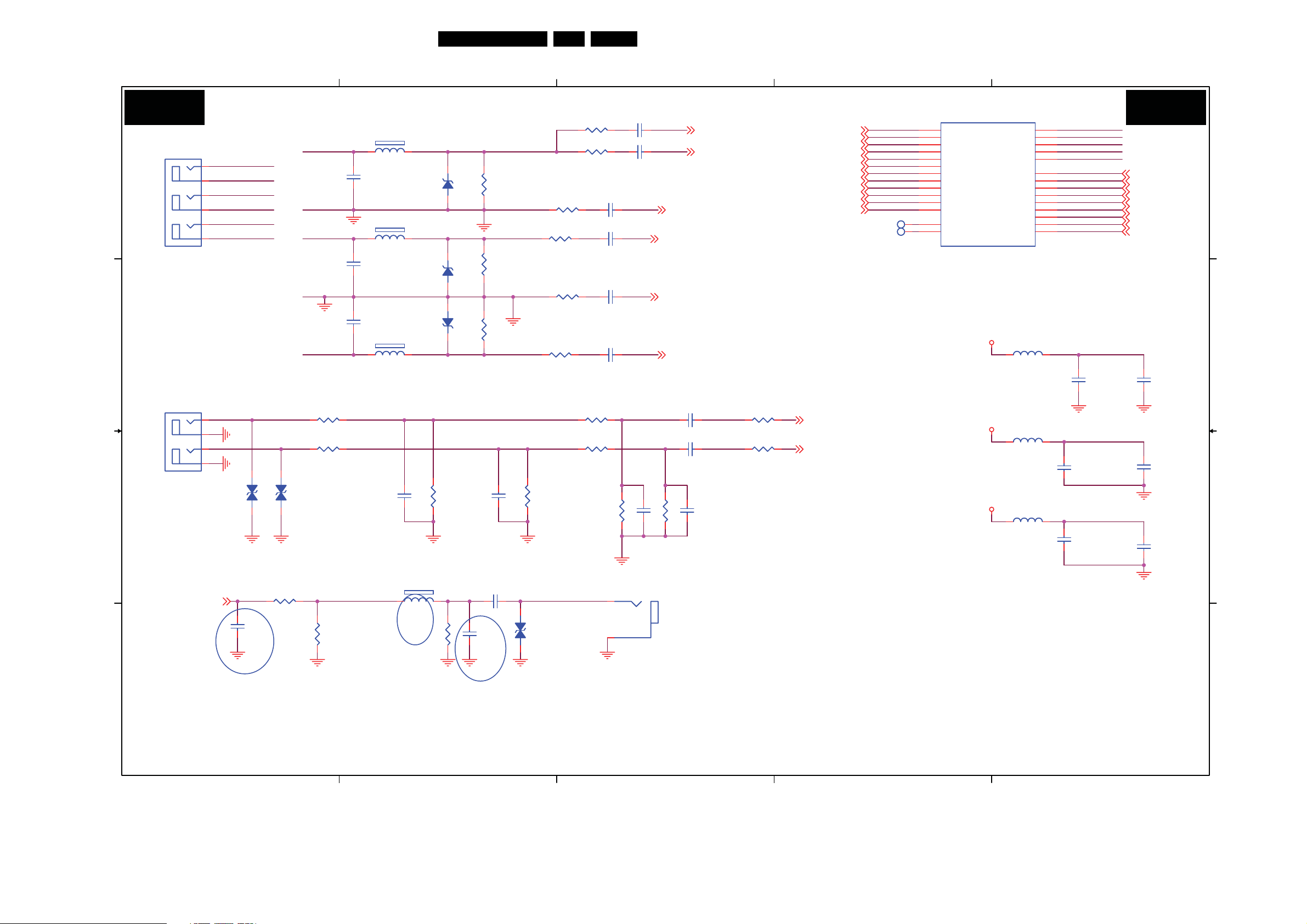
3330D/10 SSB: VGA IN/L/R
1
18TPM1.3HE LA 7.
2
3
4
5
SB01 SB01
VGA IN/L/R
CN108
CN108
1
9
2
DB15
DB15
VSYNC#
R218
R218
1K OHM 1/10W
1K OHM 1/10W
R219
R219
1K OHM 1/10W
1K OHM 1/10W
ZD131
ZD131
10
3
11
4
12
5
13
6
14
7
15
8
A
B B
C
CN109
CN109
PHONEJACK
PHONEJACK
1
2
3
VGAL_IN
VGAR_IN
ZD130
ZD130
HSYNC#
RED
GRN
BLU
HSYNC#
RED_GND
VSYNC#
GRN_GND
BLU_GND
1
L114
L114
1
80 OHM
80 OHM
UDZSNP5.6B
UDZSNP5.6B
C196
C196
5pF
5pF
L113
L113
80 OHM
80 OHM
C192
C192
5pF
5pF
UDZSNP5.6B
UDZSNP5.6B
ZD127
ZD127
VGA_PLUGPWR
R244 NCR244 NC
R245 NCR245 NC
VGASDA_IN
VGASCL_IN
2
ZD125
ZD125
2
1 2
R220
R220
3K OHM 1/10W
3K OHM 1/10W
R221
R221
3K OHM 1/10W
3K OHM 1/10W
2.2K OHM 1/10W
2.2K OHM 1/10W
1 2
R203
R203
2.2K OHM 1/10W
2.2K OHM 1/10W
R198
R198
VGASDA _IN
VGASCL_IN
C107
C107
NC/5pF
NC/5pF
C109
C109
NC/5pF
NC/5pF
U0RX SB10
U0TX SB10
HSYNC SB02,11
VSYNC SB02,11
C120 10uF/10VC120 10uF/10V
C122 10uF/10VC122 10uF/10V
R204
R204
20K OHM 1/10W
20K OHM 1/10W
R206
R206
20K OHM 1/10W
20K OHM 1/10W
GRN
GRN_GND
BLU
BLU_GND
RED
RED_GND
AIN0_L SB08
AIN0_R SB08
L111
L111
1 2
80 OHM
80 OHM
C187
C187
5pF
5pF
UDZSNP5.6B
UDZSNP5.6B
L112
L112
1
80 OHM
80 OHM
UDZSNP5.6B
UDZSNP5.6B
C190
C190
5pF
5pF
L101
L101
1 2
80 OHM
80 OHM
UDZSNP5.6B
UDZSNP5.6B
C194
C194
5pF
5pF
ZD121
ZD121
ZD124
ZD124
ZD126
ZD126
NEARLY ICNEARLY VGA CON.
VGA_PLUGPWR
Q102
Q102
MMBT3904
MMBT3904
C101 4700pFC101 4700pF
C186 0.01uF/25VC186 0.01uF/25V
C188 0.01uF/25VC188 0.01uF/25V
C189 0.01uF/25VC189 0.01uF/25V
C191 0.01uF/25VC191 0.01uF/25V
C193 0.01uF/25VC193 0.01uF/25V
C195 0.01uF/25VC195 0.01uF/25V
+5VSB
RN101
RN101
4.7KOHM +-5% 1/16W
4.7KOHM +-5% 1/16W
SOG SB02
GP SB02
GN SB02
BP SB02
BN SB02
RP SB02
RN SB02
D101 BAT54CD101 BAT54C
2
1
1
2
3
4
R165
R165
NC/0 OHM 1/10W
NC/0 OHM 1/10W
8
7
6
5
3
8
7
6
5
C197
C197
0.1UF16V
0.1UF16V
U105
U105
VCC
WC
SCL
SDA
M24C02-WDW6P
M24C02-WDW6P
VSS
1
E0
2
E1
3
E2
4
CN108 A1 CN109 C1
C101 A4 C102 A3
C103 B3 C106 B3
C107 B2 C109 C2
C120 C2 C122 C2
C135 D2 C136 D2
C181 D1 C182 D2
C186 A4 C187 A3
C188 B4 C189 B4
C190 B3 C191 B4
C192 B1 C193 B4
C194 B3 C195 C4
C196 C1 C197 C5
D101 C4 L101 B3
L111 A3 L112 B3
L113 B2 L114 C1
Q102 C4 RN101 C4
R165 D4 R188 A4
R189 A4 R191 A3
R192 B4 R193 B4
R194 B4 R195 B3
R196 B4 R197 B4
R198 B2 R199 B4
R200 B3 R201 C4
R202 C4 R203 C2
R204 C3 R205 C4
R206 C3 R207 C4
R218 C1 R219 C1
R220 C2 R221 C2
R222 D1 R223 D2
R224 D2 R225 D2
R244 A2 R245 A2
R248 C4 U105 C5
ZD121 A3 ZD124 B3
ZD125 B2 ZD126 B3
ZD127 C2 ZD128 D4
ZD129 D4 ZD13
0 D1
R188
R188
0 OHM 1/10W
0 OHM 1/10W
R189
R189
39 OHM +-1% 1/10W
39 OHM +-1% 1/10W
C102
R191
R191
1 2
2
R195
R195
1 2
R200
R200
1 2
HDMIED_WPSB12,18
VGASCL_IN
VGASDA _IN
C102
NC/5pF
NC/5pF
R192
R192
0 OHM 1/10W
75 OHM +-1% 1/8W
75 OHM +-1% 1/8W
75 OHM +-1% 1/8W
75 OHM +-1% 1/8W
75 OHM +-1% 1/8W
75 OHM +-1% 1/8W
0 OHM 1/10W
C106
C106
NC/5pF
NC/5pF
R196
R196
0 OHM 1/10W
0 OHM 1/10W
C103
C103
NC/5pF
NC/5pF
R201
R201
0 OHM 1/10W
0 OHM 1/10W
R248 10K OHM 1/10WR248 10K OHM 1/10W
ZD128
ZD128
R193
R193
100 OHM 1/10W
100 OHM 1/10W
R194
R194
39 OHM +-1% 1/10W
39 OHM +-1% 1/10W
R197
R197
100 OHM 1/10W
100 OHM 1/10W
R199
R199
39 OHM +-1% 1/10W
39 OHM +-1% 1/10W
R202
R202
100 OHM 1/10W
100 OHM 1/10W
R205 100 OHM 1/10WR205 100 OHM 1/10W
R207 100 OHM 1/10WR207 100 OHM 1/10W
ZD129
ZD129
H : WP ENABLE
L : WP DISABLE
A
C
1 2
1 2
VPORT0603100KV05
VPORT0603100KV05
VPORT0603100KV05
VPORT0603100KV05
D D
1
C181 470pFC181 470pF
R222
R222
R223
R223
C182 470pFC182 470pF
100K OHM 1/10W
100K OHM 1/10W
100K OHM 1/10W
100K OHM 1/10W
C135 33pFC135 33pF
R224
R224
30K OHM 1% 1/10W
30K OHM 1% 1/10W
2
C136 33pFC136 33pF
R225
R225
30K OHM 1% 1/10W
30K OHM 1% 1/10W
3
1 2
UDZSNP5.6B
UDZSNP5.6B
1 2
UDZSNP5.6B
UDZSNP5.6B
I_18120_026.eps
4
5
260608
Circuit Diagrams and PWB Layouts
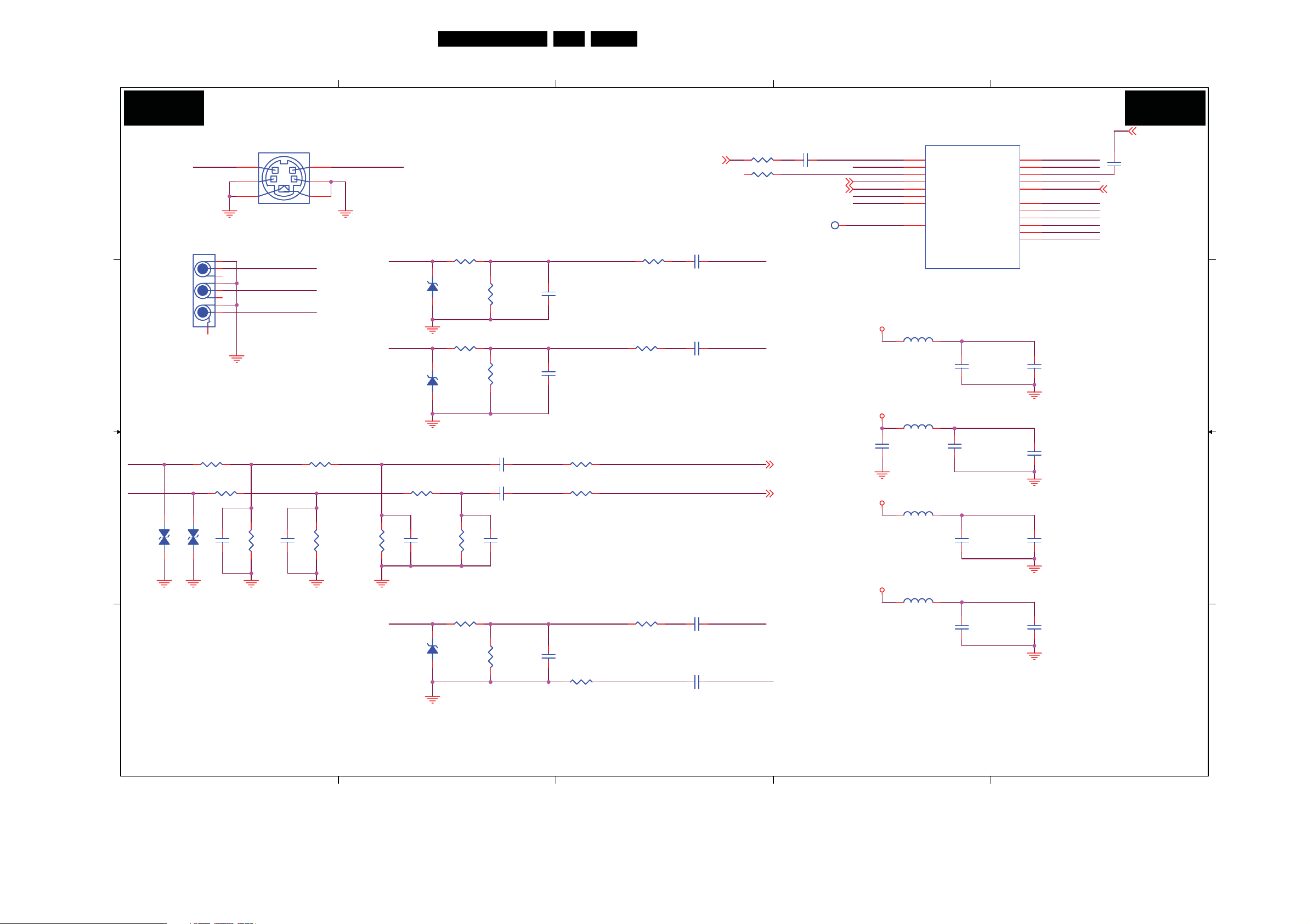
3330D/10 SSB: YPbPr/L/R & SPDIF
1
19TPM1.3HE LA 7.
2
3
4
5
SB02 SB02
CN105
CN105
A
JACK
JACK
B B
CN106
CN106
JACK
JACK
C
SB08
D
2
1
4
3
6
5
2
1
4
3
ASPDIF
PR0_IN
PB_GND
PB0_IN
PB_GND
Y0_IN
Y_GND
ZD119
ZD119
1 2
VPORT0603100KV05
VPORT0603100KV05
R183
R183
100 OHM 1/10W
100 OHM 1/10W
C119
C119
100pF
100pF
100 OHM 1/10W
100 OHM 1/10W
1/8 River
NC DVD part
Y0_IN
Y_GND
PB0_IN
PB_GND
PR0_IN
R175 1K OHM 1/10WR175 1K OHM 1/10W
R176 1K OHM 1/10WR176 1K OHM 1/10W
ZD120
ZD120
1 2
VPORT0603100KV05
VPORT0603100KV05
R185
R185
NEARLY YPBPR CONNECTOR
L108
L108
C198
C198
470pF
470pF
R184
R184
1 2
30 OHM
30 OHM
1/8 River
2
R186NCR186
NC
1
80 OHM
80 OHM
C171
C171
100pF
100pF
L109
L109
1 2
80 OHM
80 OHM
C172
C172
100pF
100pF
C173
C173
100pF
100pF
L110
L110
1 2
80 OHM
80 OHM
ZD116
ZD116
UDZSNP5.6B
UDZSNP5.6B
ZD117
ZD117
UDZSNP5.6B
UDZSNP5.6B
ZD118
ZD118
UDZSNP5.6B
UDZSNP5.6B
Change to 75 OHM 1/8W
R177
R177
100K OHM 1/10W
100K OHM 1/10W
1/8 River
Y0_IN_OUT
R209
R209
75 OHM +-1% 1/8W
75 OHM +-1% 1/8W
PB0_IN_OUT
R210
R210
75 OHM +-1% 1/8W
75 OHM +-1% 1/8W
R211
R211
75 OHM +-1% 1/8W
75 OHM +-1% 1/8W
PR0_IN_OUT
YPBPR0L_IN
YPBPR0R_IN
C199
C199
470pF
470pF
C183
C183
0.1UF16V
0.1UF16V
C185
C185
100pF
100pF
12
R105
R105
0 OHM 1/10W
0 OHM 1/10W
R106
R106
68 OHM 1/10W
68 OHM 1/10W
R107
R107
100 OHM 1/10W
100 OHM 1/10W
R108
R108
68 OHM 1/10W
68 OHM 1/10W
R110
R110
100 OHM 1/10W
100 OHM 1/10W
R111
R111
68 OHM 1/10W
68 OHM 1/10W
R129
R129
3K OHM 1/10W
3K OHM 1/10W
R130
R130
3K OHM 1/10W
3K OHM 1/10W
R178
R178
100K OHM 1/10W
100K OHM 1/10W
SPDIF_OUT
---><---|>
ZD101
ZD101
VPORT0603100KV05
VPORT0603100KV05
C104 4700pFC104 4700pF
C105 0.01uF/25VC105 0.01uF/25V
C108 0.01uF/25VC108 0.01uF/25V
C111 0.01uF/25VC111 0.01uF/25V
C114 0.01uF/25VC114 0.01uF/25V
C116 0.01uF/25VC116 0.01uF/25V
30K OHM 1/10W
30K OHM 1/10W
R243
R243
CN107
CN107
2
1
JACK
JACK
SOY1
Y1P
Y1N
PB1P
PBR1N
PR1P
NEARLY MT5335
C13110uF/10VC13110uF/10V
C13210uF/10VC13210uF/10V
C20833pFC20833pF
C209 33pFC209 33pF
30K OHM 1/10W
30K OHM 1/10W
R242
R242
R246
R246
20K OHM 1/10W
20K OHM 1/10W
R247
R247
20K OHM 1/10W
20K OHM 1/10W
SOY0SB04
Y0PSB04
Y0NSB04
PB0PSB04
PBR0NSB04
PR0PSB04
SOY1
Y1P
Y1N
PB1P
PBR1N
PR1P
AIN1_L SB08
AIN1_R SB08
U401E
SOY0
Y0P
Y0N
PB0P
PBR0N
PR0P
TP101TP101
TP106TP106
CN105 A1 CN106 B1 CN107 C3
C104 A3 C105 A3 C108 A3
C111 A3 C114 B3 C116 B3
C119 D1 C131 B3 C132 B3
C171 A2 C172 A2 C173 B2
C174 B5 C175 B5 C176 C5
C177 C5 C179 C5 C180 C5
C183 C2 C185 D2 C198 C2
C199 C2 C208 C3 C209 C3
FB101 B4 FB107 B4 FB108 C4
L108 A2 L109 A2 L110 B2
R105 A3 R106 A3 R107 A2
R108 A2 R110 B2 R111 B2
R129 B3 R130 B3 R175 B1
R176 B1 R177 C2 R178 C2
R183 C1 R184 C2 R185 D1
R186 D2 R209 A2 R210 A2
R211 B2 R242 C3 R243 C3
R246 B3 R247 B3 U401E A4
ZD101 C2 ZD116 A2 ZD117 A2
ZD118 B2
107
108
109
114
115
116
118
119
120
121
122
123
112
111
U401E
SOY0
Y0P
Y0N
PB0P
PBR0N
PR0P
SOY1
Y1P
Y1N
PB1P
PBR1N
PR1P
TN1
TP1
MT5335PGU
MT5335PGU
AVSS12_RGBADC
AVDD12_RGBADC
DVDD12_VGA
AVSS12_RGBFE
AVDD12_RGBFE
RP
RN
BP
BN
GP
GN
VSYNC
HSYNC
SOG
AV1 2
FB101
FB101
BEAD
BEAD
AV1 2
FB107
FB107
BEAD
BEAD
AV1 2
FB108
FB108
BEAD
BEAD
117
113
110
105
101
104
106
98
99
102
103
96
97
100
DVDD12_VGA
AVSS12_RGBADC
AVDD12_RGBADC
AVSS12_RGBFE
AVDD12_RGBFE
DVDD12_VGA
C174
C174
1uF/16V
1uF/16V
AVDD12_RGBADC
C176
C176
10uF/10V
10uF/10V
AVSS12_RGBADC
AVDD12_RGBFE
C179
C179
1uF/16V
1uF/16V
AVSS12_RGBFE
RP SB01
RN SB01
BP SB01
BN SB01
GP SB01
GN SB01
VSYNC SB01,11
HSYNC SB01,11
SOG SB01,11
C175
C175
0.1UF16V
0.1UF16V
C177
C177
0.1UF16V
0.1UF16V
C180
C180
0.1UF16V
0.1UF16V
YPbPr/L/R & SPDIF
A
C
D
I_18120_027.eps
1
2
3
4
5
260608
Circuit Diagrams and PWB Layouts
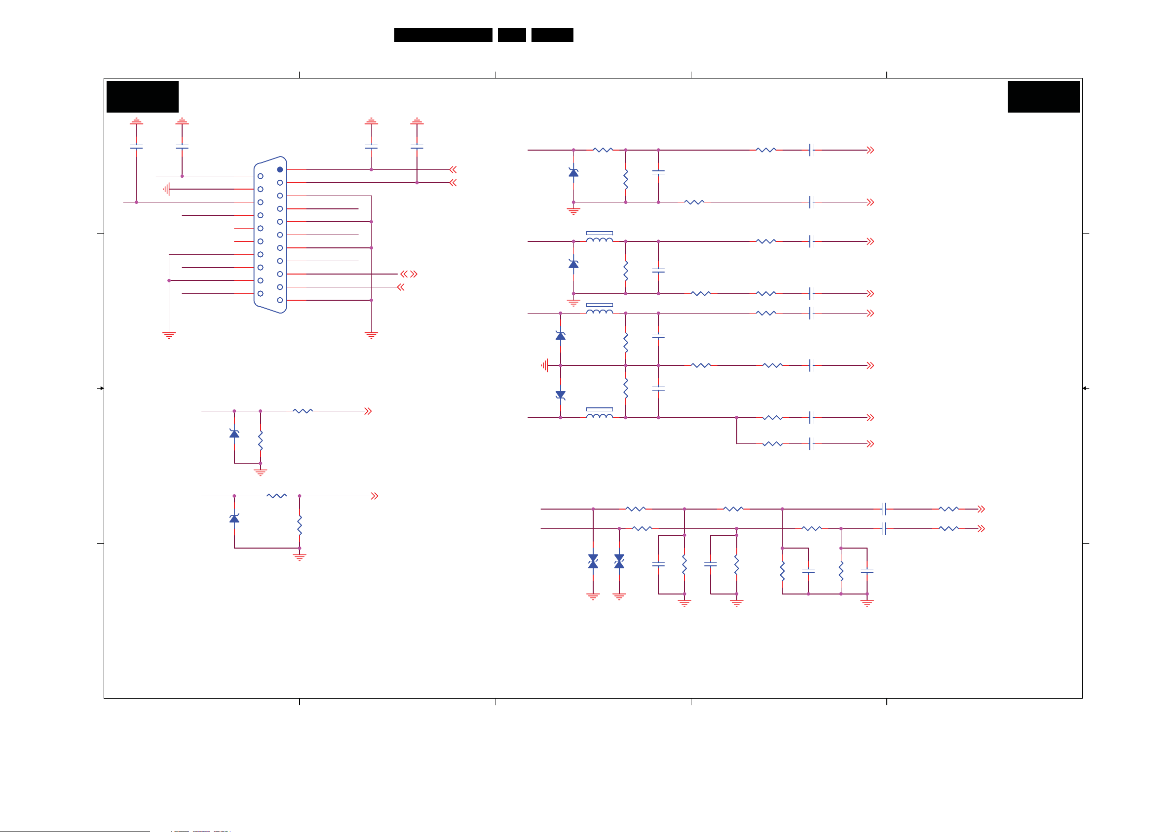
3330D/10 SSB: S-Video/CVBS/L/R
1
20TPM1.3HE LA 7.
2
3
4
5
SB03 SB03
S-VIDEO/CVBS/L/R
U401F
CN103NCCN103
SC1_IN
A A
CN104
CN104
JACK
JACK
2
B B
4
2
6
NC
7
9
8
4
6
5
1
3
AV1_IN
AV1L_IN
AV1R_IN
3
1
5
SY1_IN
SY1_IN
SC1_IN
R162NCR162
NC
ZD111NCZD111
R166NCR166
NC
ZD112NCZD112
NEARLY AV CONNECTOR NEARLY MT5380
R163NCR163
NC
NC
NC
R164NCR164
NC
R168NCR168
NC
C152NCC152
NC
C156NCC156
NC
R167NCR167
NC
CVBS0SB16
C151 NCC151 NC
C154 NCC154 NC
Near Connector
AV1R_IN
AV1 L_I N
C
D
R226 1K OHM 1/10WR226 1K OHM 1/10W
R227 1K OHM 1/10WR227 1K OHM 1/10W
ZD113
ZD113
1 2
1 2
VPORT0603100KV05
VPORT0603100KV05
VPORT0603100KV05
VPORT0603100KV05
ZD114
ZD114
C200 470pFC200 470pF
R228
R228
100K OHM 1/10W
100K OHM 1/10W
R232
R232
3K OHM 1/10W
3K OHM 1/10W
C201 470pFC201 470pF
R229
R229
100K OHM 1/10W
100K OHM 1/10W
R233
R233
3K OHM 1/10W
3K OHM 1/10W
C202 33pFC202 33pF
30K OHM 1/10W
30K OHM 1/10W
R230
R230
AV1_IN
R231
R231
R171
R171
27 OHM 1/10W
27 OHM 1/10W
ZD115
ZD115
UDZSNP5.6B
UDZSNP5.6B
C157 2.2uF/16VC157 2.2uF/16V
C160 2.2uF/16VC160 2.2uF/16V
C20333pFC20333pF
30K OHM 1/10W
30K OHM 1/10W
R173
R173
47 OHM 1/10W
47 OHM 1/10W
R169
R169
20K OHM 1/10W
20K OHM 1/10W
R170
R170
20K OHM 1/10W
20K OHM 1/10W
C167
C167
47pF
47pF
R174
R174
0 OHM 1/10W
0 OHM 1/10W
R172
R172
100 OHM 1/10W
100 OHM 1/10W
C164 0.047uFC164 0.047uF
C168 1uF/16VC168 1uF/16V
Close to MT5382p
R179
R179
100 OHM 1/10W
100 OHM 1/10W
R182NCR182
NC
SY1
SC1
AIN2_R SB08
AIN2_L SB08
CVBS1
GND_CVBS
C117
C117
0.047uF
0.047uF
CVBS1
SY0SB04
SC0SB04
SY1
SC1
D2SA
TP105TP105
AV2 5
AV2 5
C161
C161
4.7uF/10V
4.7uF/10V
AV2 5
AV2 5
132
130
129
128
127
126
125
136
FB103
FB103
BEAD
BEAD
FB104
FB104
BEAD
BEAD
FB105
FB105
BEAD
BEAD
FB106
FB106
BEAD
BEAD
U401F
CVBS0
CVBS1
CVBS2
SY0
SC0
SY1
SC1
D2SA
DVDD25_VADC
DVSS25_VADC
GND_TUNER
GD_CVBS
GND_SV
AVDD25_VADC
AVSS25_VADC
AVDD25_REF
AVSS25_REF
AVDD25_VFE
AVSS25_VFE
MT5335PGU
MT5335PGU
DVDD25_VADC
C158
C158
1uF/16V
1uF/16V
DVSS25_VADC
AVDD25_VADC
C162
C162
1uF/16V
1uF/16V
AVSS25_VADC
AVDD25_REF
C165
C165
1uF/16V
1uF/16V
AVSS25_REF
AVDD25_VFE
C169
C169
1uF/16V
1uF/16V
AVSS25_VFE
139
140
133
131
124
141
142
137
138
135
134
DVDD25_VADC
DVSS25_VADC
GND_CVBS
GND_SV
AVDD25_VADC
AVSS25_VADC
AVDD25_REF
AVSS25_REF
AVDD25_VFE
AVSS25_VFE
C159
C159
0.1UF16V
0.1UF16V
C163
C163
0.1UF16V
0.1UF16V
C166
C166
0.1UF16V
0.1UF16V
C170
C170
0.1UF16V
0.1UF16V
GND_TUNER SB16
C118
C118
1uF/16V
1uF/16V
GND_SV SB04
CN103 A1 CN104 A1
C117 A4 C118 A5
C151 A3 C152 B2
C154 B3 C156 B2
C157 C2 C158 B4
C159 B5 C160 C2
C161 B4 C162 B4
C163 C5 C164 C3
C165 C4 C166 C5
C167 D2 C168 D3
C169 D4 C170 D5
C200 C1 C201 C1
C202 C2 C203 C2
FB103 B4 FB104 B4
FB105 C4 FB106 C4
R162 A2 R163 A3
R164 B2 R166 B2
R167 B3 R168 B2
R169 C3 R170 C3
R171 C2 R172 C3
R173 D2 R174 D3
R179 A3 R182 A3
R226 C1 R227 C1
R228 C1 R229 C1
R230 C2 R231 C2
R232 C1 R233 C2
TP105 A4 U401F A4
ZD111 B2 ZD112 B2
ZD113 C1 ZD114 C1
C
D
I_18120_028.eps
1
2
3
4
5
260608
Circuit Diagrams and PWB Layouts
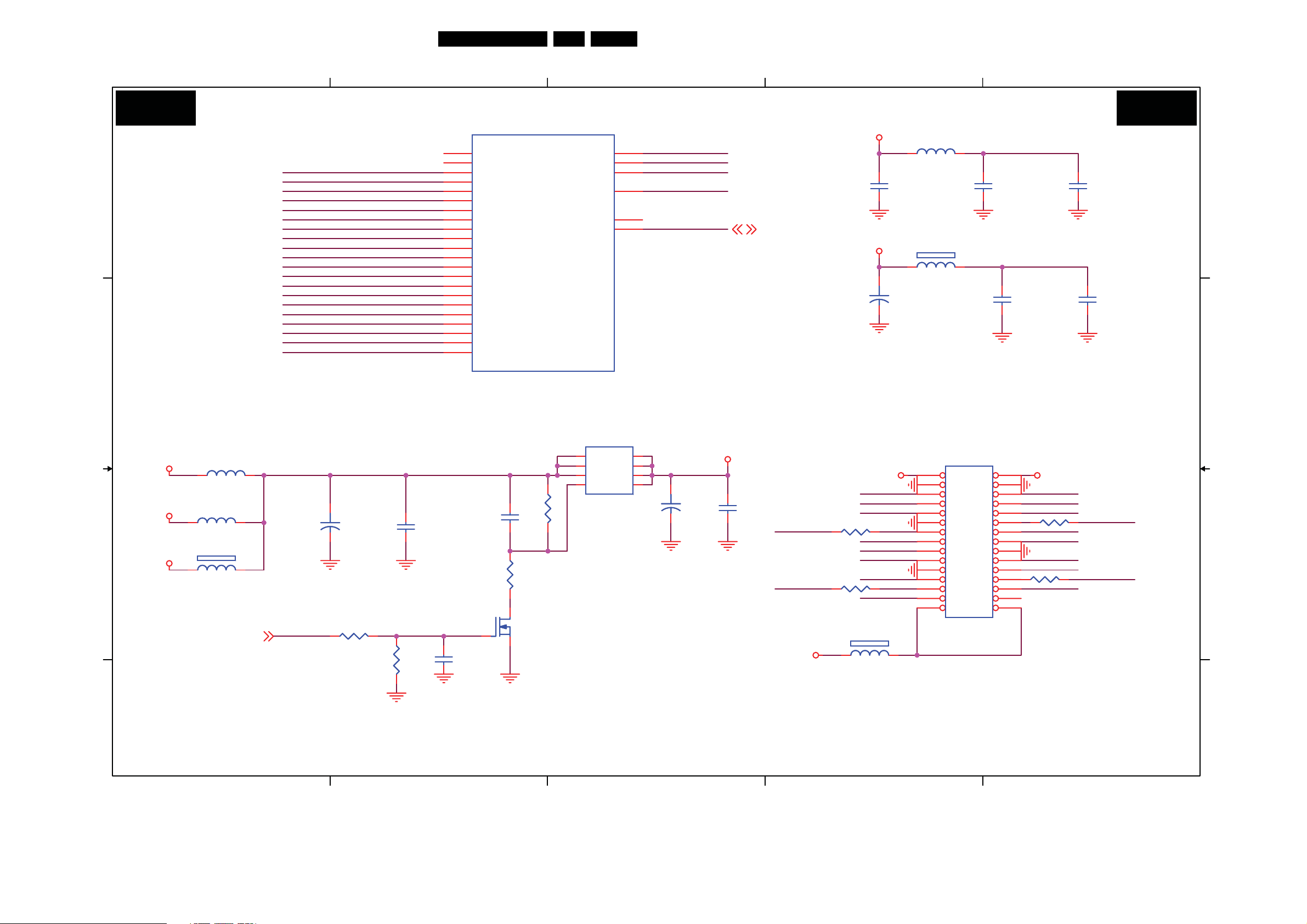
3330D/10 SSB: SCART connector
1
21TPM1.3HE LA 7.
2
3
4
5
SB04 SB04
SCART CONNECTOR
CI YLRAENROTCENNOC YLRAEN
C112
C113
C113
560pF
A
B B
560pF
C115
C115
560pF
560pF
SCT1_AUR_IN
SCT1_AUL_IN
SCT1_FS_IN
SCT1_FB_IN
SCT1_AV_IN
CN102
CN102
SCT1_AUR_OUT
2
4
6
8
10
12
14
16
18
20
1
3
5
7
9
11
13
15
17
19
21
SCART
SCART
SCT1_AUL_OUT
SCT1_B_IN
SCT1_G_IN
SCT1_R_IN
SCT1_AVO_GND
SCT1_AV_OUT
C112
1000pF/25V
1000pF/25V
SCT1_AV_OUT SB16
C110
C110
1000pF/25V
1000pF/25V
SCT1_AUR_OUT SB14
SCT1_AUL_OUT SB14
SCT1_AVO_GND SB16
SCT1_AV_IN
SCT1_G_IN
SCT1_B_IN
Full SCART
SCT1_FB_IN
ZD109
ZD109
UDZSNP5.6B
ZD110
ZD110
RLZ13B
RLZ13B
1 2
UDZSNP5.6B
C
SCT1_FS_IN
D
R155
R155
0 OHM 1/10W
0 OHM 1/10W
R157
R157
75 OHM 1/10W
75 OHM 1/10W
R158
R158
33K OHM 1/10W
33K OHM 1/10W
R161
R161
10K OHM 1/10W
10K OHM 1/10W
SOY0 SB02
SCART_FS_IN SB07
SCT1_R_IN
SCT1_AUR_IN
SCT1_AUL_IN
R142 27 OHM 1/10WR142 27 OHM 1/10W
ZD105
ZD105
UDZSNP5.6B
UDZSNP5.6B
L105
L105
1 2
80 OHM
80 OHM
ZD106
ZD106
UDZSNP5.6B
UDZSNP5.6B
L106
L106
1 2
80 OHM
80 OHM
ZD107
ZD107
UDZSNP5.6B
UDZSNP5.6B
ZD108
ZD108
L107
L107
1
UDZSNP5.6B
UDZSNP5.6B
80 OHM
80 OHM
2
Change to 75 OHM 1/8W
R238 1K OHM 1/10WR238 1K OHM 1/10W
R239 1K OHM 1/10WR239 1K OHM 1/10W
ZD132
ZD132
1 2
1 2
VPORT0603100KV05
VPORT0603100KV05
R144
R144
47 OHM 1/10W
47 OHM 1/10W
R147
R147
75 OHM 1/8W
75 OHM 1/8W
R151
R151
75 OHM 1/8W
75 OHM 1/8W
R154
R154
75 OHM 1/8W
75 OHM 1/8W
ZD133
ZD133
VPORT0603100KV05
VPORT0603100KV05
C139
C139
47pF
47pF
R145
R145
0 OHM 1/10W
0 OHM 1/10W
C142
C142
15pF/50V
15pF/50V
R148
R148
0 OHM 1/10W
0 OHM 1/10W
C145
C145
15pF/50V
15pF/50V
R152
R152
0 OHM 1/10W
0 OHM 1/10W
C147
C147
15pF/50V
15pF/50V
C207 NC/470pFC207 NC/470pF
R236
R236
3K OHM 1/10W
3K OHM 1/10W
C206 NC/470pFC206 NC/470pF
R234
R234
100K OHM 1/10W
100K OHM 1/10W
R143
R143
100 OHM 1/10W
100 OHM 1/10W
R146
R146
68 OHM 1/10W
68 OHM 1/10W
R149
R149
100 OHM 1/10W
100 OHM 1/10W
R150
R150
68 OHM 1/10W
68 OHM 1/10W
R153
R153
100 OHM 1/10W
100 OHM 1/10W
R156
R156
68 OHM 1/10W
68 OHM 1/10W
R215
R215
100 OHM 1/10W
100 OHM 1/10W
R235
R235
100K OHM 1/10W
100K OHM 1/10W
C138 0.047uFC138 0.047uF
C140 1uF/16VC140 1uF/16V
C141 0.01uF/25VC141 0.01uF/25V
C143 0.01uF/25VC143 0.01uF/25V
C144 0.01uF/25VC144 0.01uF/25V
C146 0.01uF/25VC146 0.01uF/25V
C148 0.01uF/25VC148 0.01uF/25V
C134 0.047uFC134 0.047uF
R237
R237
3K OHM 1/10W
3K OHM 1/10W
C205 33pFC205 33pF
30K OHM 1/10W
30K OHM 1/10W
R241
R241
C204 33pFC204 33pF
30K OHM 1/10W
30K OHM 1/10W
R240
R240
SY0 SB03
GND_SV SB03
Y0P SB02
Y0N SB02
PB0P SB02
PBR0N SB02
PR0P SB02
SC0 SB03
NEARLY MT5335
C149 2.2uF/16VC149 2.2uF/16V
C150 2.2uF/16VC150 2.2uF/16V
R159
R159
20K OHM 1/10W
20K OHM 1/10W
R160
R160
20K OHM 1/10W
20K OHM 1/10W
AIN3_R SB08
AIN3_L SB08
CN102 A1
C110 A2
C112 A2
C113 A1
C115 A1
C134 C4
C138 A4
C139 A3
C140 A4
C141 A4
C142 B3
C143 B4
C144 B4
C145 B3
C146 B4
C147 B3
C148 C4
C149 C4
C150 C4
C204 D4
C205 D4
C206 D3
C207 D3
L105 A3
L106 B3
L107 C3
R142 A3
R143 A4
R144 A3
R145 A3
R146 A4
R147 B3
R148 B3
R149 B4
R150 B4
R151 B3
R152 B3
R153 B4
R154 B3
R155 C1
R156 C4
R157 C1
R158 C1
R159 C5
R160 C5
R161 C1
R215 C4
R234 C3
R235 C4
R236 C4
R237 C4
R238 C3
R239 C3
R240 D4
R241 D4
ZD105 A3
ZD106 B3
ZD107 B3
ZD108 B3
ZD109 C1
ZD110 C1
ZD132 C3
ZD133 C3
A
C
D
I_18120_029.eps
1
2
3
4
5
260608
Circuit Diagrams and PWB Layouts
3330D/10 SSB: LVDS OUT
1
22TPM1.3HE LA 7.
2
3
4
5
SB05 SB05
A A
B
LVD S OUT
A0N
A0P
A1N
A1P
A2N
A2P
CK1N
CK1P
A3N
A3P
A4N
A4P
A5N
A5P
A6N
A6P
CK2N
CK2P
A7N
A7P
244
243
242
241
240
239
237
236
235
234
233
232
231
230
228
227
226
225
224
223
222
221
U401C
U401C
A0N
A0P
A2N
A2P
CK1N
CK1P
A3N
A3P
A4N
A4P
A5N
A5P
A6N
A6P
A7N
A7P
CK2N
CK2P
A8N
A8P
A9N
A9P
MT5335PGU
MT5335PGU
AVD D33_LVDSA
AVD D33_LVDSB
AVD D33_LVDSC
AVD D33_VPLL
TP2
TN2
220
229
238
217
218
219
AVDD33_LVDS
AVDD33_LVDS
AVDD33_LVDS
AVDD33_VPLL
CI_POCE1# SB18
AV33
AV33
+
+
FB301
FB301
BEAD
BEAD
C303
C303
1uF/16V
1uF/16V
FB302
FB302
1 2
BEAD
BEAD
C305
C305
100uF/16V
100uF/16V
AVD D33_LVDS
C302
C302
10uF/10V
10uF/10V
AVD D33_VPLL
C306
C306
1uF/16V
1uF/16V
C304
C304
0.1UF16V
0.1UF16V
C307
C307
0.1UF16V
0.1UF16V
CN301 B4
C301 C2
U301
DV33
16V
+5V
C
3A
L301NCL301
NC
L302NCL302
NC
1 2
L303
L303
BEAD
BEAD
+
+
HI = > LVDS POWER ON
LVD S OUT
C310
C310
220uF/16V
220uF/16V
C311
C311
0.1UF16V
0.1UF16V
C312
C312
NC/1uF/16V
NC/1uF/16V
R302
R302
100K OHM 1/10W
100K OHM 1/10W
R305
R305
10K OHM 1/10W
10K OHM 1/10W
U301
1
S
2
3
4
AO4449 -7A/-30V
AO4449 -7A/-30V
D
D
S
D
S
G
D
8
7
6
5
+
+
C308
C308
NC/100uF/16V
NC/100uF/16V
LO = > LVDS POWER OFF
Q301
LV DSVDD_ENSB07
R306 51K OHM 1/10WR306 51K OHM 1/10W
R307
1M OHM 1/10W
1M OHM 1/10W
R307
C301
C301
1uF6.3V
1uF6.3V
Q301
2N7002 SOT-23
2N7002 SOT-23
LV DSVDD
C309
C309
0.1UF16V
0.1UF16V
CK1P
CK2P
DV33
LV DSVDD
A0N A0P
A1N A1P
A2N A2P
R308 22 OHM 1/10WR308 22 OHM 1/10W
R310 22 OHM 1/10WR310 22 OHM 1/10W
A3P
A4P
A5N A5P
A6P
A7P
FB303
FB303
1 2
NC/220 OHM
NC/220 OHM
CN301
CN301
1 2
3 4
5 6
7 8
9
11
13
15 16
17
19
21 22
23
25
27
29
CONN
CONN
10
R309 22 OHM 1/10WR309 22 OHM 1/10W
12
14
18
20
R311 22 OHM 1/10WR311 22 OHM 1/10W
24
26
28
30
A3N
A4N
A6N
A7N
LV DSVDD
CK1N
CK2N
C302 A4
C303 A4
C304 A5
C305 B4
C306 B4
C307 B5
C308 C3
C309 C3
C310 C1
C311 C2
C312 C2
FB301 A4
FB302 A4
FB303 C4
L301 B1
L302 C1
L303 C1
Q301 C2
R302 C2
R305 C2
R306 C2
R307 C2
R308 C4
R309 C5
R310 C4
R311 C5
U301 B3
U401C A2
B
C
D
1
2
3
4
5
I_18120_030.eps
D
260608
Circuit Diagrams and PWB Layouts
3330D/10 SSB: MT5335 HDMI/PLL
1
23TPM1.3HE LA 7.
2
3
4
5
SB06 SB06
U401D
USB_VRT
USB_D-SB10
USB_D+
SB10
A
B
C
SB18
TS_VALIDOSB18
TS_CKO
SB13
SB13
SB13
USB_DUSB_D+
AVD D33_USB
AVD D12 _USB
USB_VRT
MPX0PSB16
MPX0NSB16
RX0_CBSB13
RX0_CSB13
RX0_0BSB13
RX0_0
RX0_1BSB13
RX0_1
RX0_2BSB13
RX0_2
TP409TP409
TP410TP410
R470 5.1K OHM 1/10WR470 5.1K OHM 1/10W
RX0_CB
RX0_C
RX0_0B
RX0_0
RX0_1B
RX0_1
RX0_2B
RX0_2
68
65
66
67
69
157
158
TP411TP411
U401D
USB_VRT
USB_DM
USB_DP
AVD D33_USB
AVD D12 _USB
TP0
TN0
MT5335PGU
MT5335PGU
U401H
U401H
164
SIFP
166
SIFN
167
AF
195
TUNER_DATA
194
TUNER_CLK
MT5335PGU
MT5335PGU
U401K
U401K
79
RX0_CB
80
RX0_C
81
RX0_0B
82
RX0_0
83
RX0_1B
84
RX0_1
85
RX0_2B
86
RX0_2
AVDD12_ADCPLL
AVDD12_TVDPLL
AVD D12 _SYSPLL
AVDD12_DTDPLL
AVD D25 _SADC
AVSS25_SADC
RF_AGC
IF_AGC
EXT_RES
OPWR0_5V
AVD D33_HDMI
AVDD12_CVCC
AVDD12_HDMIPLL
AVDD12_APLL
AVDD12_DMPLL
163
165
193
192
77
73
78
74
160
155
153
161
159
156
154
AVDD25_SADC
AVSS25_SADC
AVD D33_H
AVDD12_CVCC
AVDD12_PLL
AVDD12_PLL
AVDD12_PLL
AVDD12_PLL
AVDD12_PLL
AVDD12_PLL
AVDD12_PLL
TS_DATAO SB18
TS_SYNCO SB18
TP401TP401
HDMI_5V
AV1 2
AV33
FB411
FB411
BEAD
BEAD
C502
C502
1uF/16V
1uF/16V
FB401
FB401
BEAD
BEAD
01/18 Modify
AV1 2
AV2 5
AV33
AV1 2
FB412
FB412
BEAD
BEAD
C508
C508
10uF/10V
10uF/10V
FB413
FB413
BEAD
BEAD
C511
C511
1uF/16V
1uF/16V
C517
C517
1uF/16V
1uF/16V
C518
C518
1uF/16V
1uF/16V
FB414
FB414
BEAD
BEAD
FB415
FB415
BEAD
BEAD
AVDD12_PLL
C503
C503
4.7uF/10V
4.7uF/10V
AVDD33_USB
C506
C506
4.7uF/10V
4.7uF/10V
AVDD12_USB
C509
C509
4.7uF/10V
4.7uF/10V
AVDD25_SADC
C512
C512
4.7uF/10V
4.7uF/10V
AVSS25_SADC
AVDD33_H
C515
C515
4.7uF/10V
4.7uF/10V
AVDD12_CVCC
C519
C519
4.7uF/10V
4.7uF/10V
C504
C504
0.01uF/25V
0.01uF/25V
C507
C507
0.1UF16V
0.1UF16V
C510
C510
0.1UF16V
0.1UF16V
C513
C513
0.01uF/25V
0.01uF/25V
C516
C516
0.1UF16V
0.1UF16V
C520
C520
0.1UF16V
0.1UF16V
C505
C505
0.1UF16V
0.1UF16V
0.1UF16V
0.1UF16V
C514
C514
C502 A4
C503 A4
C504 A5
C505 A5
C506 B4
C507 B5
C508 B4
C509 B4
C510 B5
C511 C4
C512 C4
C513 C5
C514 C5
C515 C4
C516 C5
C517 C4
C518 D4
C519 D4
C520 D5
FB401 A4
FB411 A4
FB412 B4
FB413 B4
FB414 C4
FB415 C4
R470 A1
U401D A1
U401H C2
U401K C2
MT5335 HDMI/PLL
A
B
C
MT5335PGU
MT5335PGU
D
1
2
3
4
5
I_18120_031.eps
D
260608
Circuit Diagrams and PWB Layouts
0
3330D/10 SSB: MT5335 Control/IR/LED
1
24TPM1.3HE LA 7.
2
3
4
5
SB07 SB07
A
R492
R492
BL_DIMSB19
SB18
OPWM1
B
MT5335 CONTROL/IR/LED/KEY
U401B
R493
R493
4.7K OHM 1/10W
4.7K OHM 1/10W
4.7K OHM 1/10W
4.7K OHM 1/10W
KEY2
KEY1_MT5335
OSDA0SB13,19
SB13,19
OSCL0
SB13
OSDA1
OSCL1SB13
OPWM2SB10,18
SB18
MTK_IC_RESET
R488 33 OHM 1/10WR488 33 OHM 1/10W
SCART_FS_INSB04
POWER_ON/OFFSB19
OSDA0
OSCL0
OXTALO
OXTALI
AVCC_SRV
AVD D33_XTAL
PWRDET
AVDD33_REG
C_XREG
ORESET#
204
205
191
202
203
146
143
144
147
145
152
151
150
149
148
63
62
88
87
71
72
U401B
OSDA0
OSCL0
OSDA1
OSCL1
OPWM0
OPWM1
OPWM2
VCXO
XTALO
XTALI
AVDD33_SRV
AVDD33_XTAL
ADIN4
ADIN3
ADIN2
ADIN1
ADIN0
AVD D33_REG
C_XREG
ORESET_
OPWRSB
MT5335PGU
MT5335PGU
GPIO_3
GPIO_4
GPIO_5
GPIO_6
GPIO_7
GPIO_8
GPIO_9
GPIO_10
GPIO_11
GPIO_12
GPIO_13
OPCTRL0
OPCTRL1
OPCTRL2
OPCTRL3
OPCTRL4
OPCTRL5
207
208
209
59
60
210
211
212
214
215
216
92
91
76
75
90
89
LVD SVDD_EN SB05
AMP_MUTE SB15
BL_ON/OFF SB19
EDID_PRT
R426
R426
4.7K OHM 1/10W
4.7K OHM 1/10W
+3V3SB
CI_PDD3SB18
CI_PDD4 SB18
CI_PDD5 SB18
CI_PDD6 SB18
CI_PDD7 SB18
CI_POWE# SB18
CI_OEB SB18
CI_ALE SB18
CI_CLE SB18
CI_INT SB18
+3V3SB
+3V3SB
DV33
R448
R448
1K OHM 1/10W
1K OHM 1/10W
PWRDET
C_XREG
R454 1 OHM +-5% 1/10WR454 1 OHM +-5% 1/10W
The divider only for A version IC
C491
C491
4.7uF/10V
4.7uF/10V
D401
D401
LL4148
LL4148
Adjust the power on timing
C488
C488
+
+
220uF/10V
220uF/10V
R449
R449
220 OHM 1/10W
220 OHM 1/10W
R450
R450
47K OHM 1/10W
47K OHM 1/10W
For OTS
+3V3SB +3V3SB
R444
10K OHM 1/10W
10K OHM 1/10W
HDMI_INTSB11
C
R444
10K OHM 1/10W
10K OHM 1/10W
Q403
Q403
MMBT3904
MMBT3904
EDID_PRT
R445
R445
CECSB11,12
R456
R456
10K OHM 1/10W
10K OHM 1/10W
R420
R420
NC/0 OHM 1/10W
NC/0 OHM 1/10W
R461 10K OHM 1/10WR461 10K OHM 1/10W
R463
R463
10K OHM 1/10W
10K OHM 1/10W
DV33
Q406
Q406
MMBT3904
MMBT3904
R486NCR486
NC
R495
R495
0 OHM 1/10W
0 OHM 1/10W
R459
R459
33 OHM 1/10W
33 OHM 1/10W
OSCL0
OSDA0
Q408
Q408
NC/MMBT3904
NC/MMBT3904
R487NCR487
NC
U405
U405
8
NC
VCC
7
NC
WC
6
NC
SCL
5
SDA
VSS
M24C16
M24C16
IIC ADDRESS "A0"
DV33
C492
1
2
3
4
C492
1uF/16V
1uF/16V
TURN_ONSB11
STANDBYSB11
TURN_ON
STANDBY
1/8 River
+5V
C441
C441
1000pF/25V
1000pF/25V
C452
C452
1000pF/25V
1000pF/25V
+3V3SB_uP
+3V3SB_uP
+3V3SB
R427
R427
R453
R453
0 OHM 1/10W
0 OHM 1/10W
R455
R455
0 OHM 1/10W
0 OHM 1/10W
C493
C493
4.7uF/10V
4.7uF/10V
R447
R447
1K OHM 1/10W
1K OHM 1/10W
ORESET#
Q404
Q404
MMBT3904
MMBT3904
+3V3SB +5VSB
ORESET#
2
R462
R462
NC/1K OHM 1/10W
NC/1K OHM 1/10W
NC/3K OHM 1/10W
NC/3K OHM 1/10W
+5VSB
OXTALI
Third-Tone Crystal
R497NCR497
R498
R498
NC/6.2K OHM 1/10W
NC/6.2K OHM 1/10W
NC
3
U408
U408
NC/MAX809STRG
NC/MAX809STRG
VCC
RESET
GND
1
+3V3SB_uP
R460
NC/1K OHM 1/10W
R460
NC/1K OHM 1/10W
Q405
Q405
NC/MMBT3906
NC/MMBT3906
R452 NCR452 NC
R446 NCR446 NC
2
C489
C489
10pF
10pF
R499
R499
NC/13K OHM 1% 1/10W
NC/13K OHM 1% 1/10W
+5V
R428
NC/1K OHM 1/10W
R428
NC/1K OHM 1/10W
OIRISB10,11
+3V3SB_uP
Y401
Y401
60MHz
60MHz
10
11
1
2
3
4
5
6
7
8
9
TXC
1
CN404
CN404
OXTALO
C490
C490
10pF
10pF
CN404 C5 C401 A5
C441 C4 C452 C4
C488 A4 C489 A5
C490 A5 C491 B3
C492 C3 C493 C4
94 D1 C495 D1
C496 D4 C497 D4
C498 D2 C499 D2
C500 D1 C501 D1
D401 A3 D403 D3
FB408 C1 FB409 D2
FB410 D1 L401 A5
Q403 B1 Q404 A4
Q405 B4 Q406 C2
Q408 B2 R420 C2
R426 B2 R427 B4
R428 B5 R444 B1
R445 B2 R446 A5
R447 A4 R448 A3
R449 A4 R450 A4
R452 C4 R453 C4
R454 B3 R455 C4
R456 C2 R458 C4
R459 C2 R460 B4
R461 C2 R462 B4
R463 C2 R464 C2
R465 C2 R466 C4
R467 C4 R468 D4
R469 D4 R486 B2
R487 B3 R488 A1
R489 C4 R492 A1
R493 A1 R495 B2
R497 A4 R498 A4
R499 B5 U401B A2
U405 C3 U408 B4
1 A5 ZD410 D5
CONN
CONN
L401
L401
0.82UH
0.82UH
C401
C401
1000pF
1000pF
+3V3SB_uP
R464
R464
R465
R465
4.7K OHM 1/10W
4.7K OHM 1/10W
4.7K OHM 1/10W
4.7K OHM 1/10W
DV33
KEY1
+3V3SB
+3V3SB
D D
FB408
FB408
BEAD
BEAD
FB410
FB410
BEAD
BEAD
1
C494
C494
1uF/16V
1uF/16V
AVCC_SRV
AVDD33_XTAL
C500
C500
1uF/16V
1uF/16V
C495
C495
0.1UF16V
0.1UF16V
C501
C501
0.1UF16V
0.1UF16V
+3V3SB
FB409
FB409
BEAD
BEAD
AVDD33_REG
C498
C498
1uF/16V
1uF/16V
2
C499
C499
0.1UF16V
0.1UF16V
KEY1_MT5335
D403
D403
2
SCS140V
SCS140V
1
3
KEY1
1/3 River
KEY1SB11
KEY2
R458NCR458
NC
+3V3SB_uP
R489NCR489
NC
C496
C496
1000pF
1000pF
R467
R467
100 OHM 1/10W
100 OHM 1/10W
C497
C497
1000pF
1000pF
4
R466 100 OHM 1/10WR466 100 OHM 1/10W
R468
470K OHM 1/10W
470K OHM 1/10W
R468
R469
R469
100K OHM 1/10W
100K OHM 1/10W
Keypad
power
ZD410
ZD410
NC/UDZSNP5.6B
NC/UDZSNP5.6B
1 2
ZD411
ZD411
NC/UDZSNP5.6B
NC/UDZSNP5.6B
5
1 2
I_18120_032.eps
260608
A
B
C
 Loading...